EP4290739B1 - Sensoranordnung für eine fremdkörperdetektionsvorrichtung - Google Patents
Sensoranordnung für eine fremdkörperdetektionsvorrichtung Download PDFInfo
- Publication number
- EP4290739B1 EP4290739B1 EP23204735.7A EP23204735A EP4290739B1 EP 4290739 B1 EP4290739 B1 EP 4290739B1 EP 23204735 A EP23204735 A EP 23204735A EP 4290739 B1 EP4290739 B1 EP 4290739B1
- Authority
- EP
- European Patent Office
- Prior art keywords
- input
- output
- sensor arrangement
- sense
- coil
- Prior art date
- Legal status (The legal status is an assumption and is not a legal conclusion. Google has not performed a legal analysis and makes no representation as to the accuracy of the status listed.)
- Active
Links
Images

Classifications
-
- H—ELECTRICITY
- H02—GENERATION; CONVERSION OR DISTRIBUTION OF ELECTRIC POWER
- H02J—CIRCUIT ARRANGEMENTS OR SYSTEMS FOR SUPPLYING OR DISTRIBUTING ELECTRIC POWER; SYSTEMS FOR STORING ELECTRIC ENERGY
- H02J50/00—Circuit arrangements or systems for wireless supply or distribution of electric power
- H02J50/005—Mechanical details of housing or structure aiming to accommodate the power transfer means, e.g. mechanical integration of coils, antennas or transducers into emitting or receiving devices
-
- G—PHYSICS
- G01—MEASURING; TESTING
- G01V—GEOPHYSICS; GRAVITATIONAL MEASUREMENTS; DETECTING MASSES OR OBJECTS; TAGS
- G01V3/00—Electric or magnetic prospecting or detecting; Measuring magnetic field characteristics of the earth, e.g. declination, deviation
- G01V3/08—Electric or magnetic prospecting or detecting; Measuring magnetic field characteristics of the earth, e.g. declination, deviation operating with magnetic or electric fields produced or modified by objects or geological structures or by detecting devices
- G01V3/10—Electric or magnetic prospecting or detecting; Measuring magnetic field characteristics of the earth, e.g. declination, deviation operating with magnetic or electric fields produced or modified by objects or geological structures or by detecting devices using induction coils
- G01V3/101—Electric or magnetic prospecting or detecting; Measuring magnetic field characteristics of the earth, e.g. declination, deviation operating with magnetic or electric fields produced or modified by objects or geological structures or by detecting devices using induction coils by measuring the impedance of the search coil; by measuring features of a resonant circuit comprising the search coil
-
- H—ELECTRICITY
- H02—GENERATION; CONVERSION OR DISTRIBUTION OF ELECTRIC POWER
- H02J—CIRCUIT ARRANGEMENTS OR SYSTEMS FOR SUPPLYING OR DISTRIBUTING ELECTRIC POWER; SYSTEMS FOR STORING ELECTRIC ENERGY
- H02J50/00—Circuit arrangements or systems for wireless supply or distribution of electric power
- H02J50/10—Circuit arrangements or systems for wireless supply or distribution of electric power using inductive coupling
-
- H—ELECTRICITY
- H02—GENERATION; CONVERSION OR DISTRIBUTION OF ELECTRIC POWER
- H02J—CIRCUIT ARRANGEMENTS OR SYSTEMS FOR SUPPLYING OR DISTRIBUTING ELECTRIC POWER; SYSTEMS FOR STORING ELECTRIC ENERGY
- H02J50/00—Circuit arrangements or systems for wireless supply or distribution of electric power
- H02J50/40—Circuit arrangements or systems for wireless supply or distribution of electric power using two or more transmitting or receiving devices
- H02J50/402—Circuit arrangements or systems for wireless supply or distribution of electric power using two or more transmitting or receiving devices the two or more transmitting or the two or more receiving devices being integrated in the same unit, e.g. power mats with several coils or antennas with several sub-antennas
-
- H—ELECTRICITY
- H02—GENERATION; CONVERSION OR DISTRIBUTION OF ELECTRIC POWER
- H02J—CIRCUIT ARRANGEMENTS OR SYSTEMS FOR SUPPLYING OR DISTRIBUTING ELECTRIC POWER; SYSTEMS FOR STORING ELECTRIC ENERGY
- H02J50/00—Circuit arrangements or systems for wireless supply or distribution of electric power
- H02J50/60—Circuit arrangements or systems for wireless supply or distribution of electric power responsive to the presence of foreign objects, e.g. detection of living beings
-
- Y—GENERAL TAGGING OF NEW TECHNOLOGICAL DEVELOPMENTS; GENERAL TAGGING OF CROSS-SECTIONAL TECHNOLOGIES SPANNING OVER SEVERAL SECTIONS OF THE IPC; TECHNICAL SUBJECTS COVERED BY FORMER USPC CROSS-REFERENCE ART COLLECTIONS [XRACs] AND DIGESTS
- Y02—TECHNOLOGIES OR APPLICATIONS FOR MITIGATION OR ADAPTATION AGAINST CLIMATE CHANGE
- Y02T—CLIMATE CHANGE MITIGATION TECHNOLOGIES RELATED TO TRANSPORTATION
- Y02T10/00—Road transport of goods or passengers
- Y02T10/60—Other road transportation technologies with climate change mitigation effect
- Y02T10/70—Energy storage systems for electromobility, e.g. batteries
-
- Y—GENERAL TAGGING OF NEW TECHNOLOGICAL DEVELOPMENTS; GENERAL TAGGING OF CROSS-SECTIONAL TECHNOLOGIES SPANNING OVER SEVERAL SECTIONS OF THE IPC; TECHNICAL SUBJECTS COVERED BY FORMER USPC CROSS-REFERENCE ART COLLECTIONS [XRACs] AND DIGESTS
- Y02—TECHNOLOGIES OR APPLICATIONS FOR MITIGATION OR ADAPTATION AGAINST CLIMATE CHANGE
- Y02T—CLIMATE CHANGE MITIGATION TECHNOLOGIES RELATED TO TRANSPORTATION
- Y02T10/00—Road transport of goods or passengers
- Y02T10/60—Other road transportation technologies with climate change mitigation effect
- Y02T10/7072—Electromobility specific charging systems or methods for batteries, ultracapacitors, supercapacitors or double-layer capacitors
-
- Y—GENERAL TAGGING OF NEW TECHNOLOGICAL DEVELOPMENTS; GENERAL TAGGING OF CROSS-SECTIONAL TECHNOLOGIES SPANNING OVER SEVERAL SECTIONS OF THE IPC; TECHNICAL SUBJECTS COVERED BY FORMER USPC CROSS-REFERENCE ART COLLECTIONS [XRACs] AND DIGESTS
- Y02—TECHNOLOGIES OR APPLICATIONS FOR MITIGATION OR ADAPTATION AGAINST CLIMATE CHANGE
- Y02T—CLIMATE CHANGE MITIGATION TECHNOLOGIES RELATED TO TRANSPORTATION
- Y02T90/00—Enabling technologies or technologies with a potential or indirect contribution to GHG emissions mitigation
- Y02T90/10—Technologies relating to charging of electric vehicles
- Y02T90/14—Plug-in electric vehicles
Definitions
- the invention relates to a sensor arrangement for a foreign object detection device for a wireless power transfer system, including (i) a current input and a current output, (ii) a multitude of detection cells, each comprising a sense coil including a winding spirally wound in a plane and having a multitude of turns, wherein the sense coils are arranged in one or more layers and wherein the sense coils of a particular layer are arranged in a matrix-like structure with multiple rows and columns, (iii) a multitude of input leads and one or more output leads, wherein each detection cell is connected between one of the input leads and one output lead and wherein each detection cell is connected to a different combination of input and output leads, and (iv) an input selection circuit adapted to selectively establish an electrical connection between the current input and one or more of the input leads.
- the invention further relates to a foreign object detection device for a primary part of a wireless power transfer system for transferring power over an air gap to a nearby receiver, including such a sensor arrangement and a primary part for a wireless power transfer system for transferring power over an air gap to a nearby receiver including such a sensor arrangement or such a foreign object detection device.
- the power classes of wireless charging systems have a wide spectrum with an output power between 1 W and several 100 kW.
- a particular detection cell may be connected to a stimulation unit and to a measurement unit by means of an input multiplexer and an output multiplexer respectively using connecting lines that are fed along the rows and columns of the matrix formed by the detection cells and where the connecting lines are connected to the input and output terminals by controllable switches.
- Foreign objects are detected by applying a stimulation signal provided by the stimulation unit to a selected detection cell, measuring the resulting response and, comparing the resulting response to a response of that detection cell to the same stimulation signal that has previously been recorded ensuring that no foreign object is positioned in the magnetic field, and if the resulting response is different from the previously recorded response, concluding that a foreign object is present in the magnetic field.
- the stimulation signal may for example be a current step.
- the resulting step response caused by this current step is an oscillation of the voltage.
- This oscillation may be defined by several parameters, which thus may be influenced by a foreign object.
- a foreign object may for example change the inductance L and the resistance R of a sense coil.
- the stimulation signal may also be a rectangular pulse or any other signal that allows to determine the property desired or needed for the detection of a foreign object.
- the sense coil of each of these multiple detection cells has not the same sensitivity across the whole surface that this particular sense coil covers.
- a sense coil having a generally square shape with an even distribution of the turns such as for example shown in fig. 8a and 8b of EP 3 734 801 , the sensitivity of the sense coil reaches a maximum at the centre of the coil and drops almost linearly to the edges of the coil.
- a foreign object positioned for example between the edges of two neighbouring sense coils may not be detected due to the reduced sensitivity of the sense coil in that area.
- a sense coil having a generally square shape where the turns are concentrated in an outer region of the coil such as for example shown in fig. 8c of EP 3 734 801 , the sensitivity of the sense coil reaches a maximum at about half the distance between the centre of the coil and the edges of the coil, has a drop around the centre of the coil and also drops from the maximum almost linearly to the edge of the coil.
- a foreign object positioned for example in the centre of such a sense coil may not be detected due to the reduced sensitivity of the sense coil in its centre and it is difficult to interpret the signals indicating the detection of a foreign object which is why the system is typically designed for the worst case scenario and thus usually has to be oversized.
- the input lead and the output lead of at least one sense coil is routed through the matrix-like structure to which the at least one sense coil belongs close to each other such as to reduce an area parallel to said matrix-like structure and enclosed by said input and output leads.
- the sense coil of at least one detection cell may include an outer coil section and an inner coil section arranged inside the outer coil section, wherein a first distance between an outermost turn of the inner coil section and an innermost turn of the outer coil section may be at least twice a largest distance between two turns of the outer region.
- the sense coil of all detection cells may include an outer coil section and an inner coil section arranged inside the outer coil section, wherein a first distance between an outermost turn of the inner coil section and an innermost turn of the outer coil section may be at least three times a largest distance between two turns of the outer region.
- the sensitivity of the sense coil can be made more uniform around the centre of the sense coil.
- the outer coil section may thereby correspond to a concentration of the windings in the outer region where the inner coil section may ensure that there is no or no substantial drop in sensitivity around the centre of the sense coil.
- an FOD according to the invention further includes a stimulus circuit for generating a predetermined stimulation signal such as for example a current step or a current pulse.
- the stimulation signal may also be a sinusoidal signal.
- the stimulus circuit is connected to a current input of the sensor arrangement. Accordingly, the current input is a connection point of the sensor arrangement where the current of the stimulation signal flows into the sensor arrangement. Similarly, the current output is a connection point of the sensor arrangement where the current of the stimulation signal flows out of the sensor arrangement. Often, the current output is connected to ground.
- An input lead is an electrical connection connecting a detection cell to an input selection circuit as described further below, where the input selection circuit then establishes the electrical connection between the current input and one or more input leads.
- an output lead is an electrical connection connecting a detection cell either directly to the current output of the sensor arrangement or to an output selection circuit as described further below, where the output selection circuit then establishes the electrical connection between one or more output leads and the current output.
- the input and output leads may be formed by any suitable electrical conductor such as for example a wire. Usually, the input leads are however formed by traces on a PCB.
- the FOD further includes a measurement unit, adapted to sense an electrical signal applied to the current input, wherein the measurement unit includes an analogue to digital converter for acquiring sampling data representing the sensed electrical signal.
- the FOD also includes a signal-processing unit, which is configured to determine time response data of a selected detection cell, based on sampling data acquired by the measurement unit. It is further preferred, that the measurement unit includes a filter for filtering the electrical signal.
- the sense coils are for example arranged as a flat structure such as a mat or plate that is positioned above the primary pad for the generation of the power transfer field and such that it is arranged between the primary and the secondary pad when the device including the secondary pad is positioned to receive power through the power transfer field.
- a wireless power transfer system is a system that allows power transfer without wires as a physical link across a space via a time-varying electromagnetic field.
- the power transfer system includes a primary part as transmitter device, driven by electric power from a power source, which generates the electromagnetic field, and a secondary part as a receiver device, which extracts power from the field and supplies it to an electrical load.
- the wireless power transfer system is an inductive power transfer system.
- the electromagnetic field which is also referred to as power transfer field, is generated by at least one resonator arranged in the primary part of the power transfer system.
- the shape of the power transfer field depends on the elements of the resonator and how they are arranged and interconnected.
- a resonator usually includes a resonating circuit with at least one coil and a capacitor.
- the resonator may also include other elements such as for example an additional inductor and one or more flux guiding elements.
- a so-called double D arrangement is often used in a resonator to generate the power transfer field.
- Such an arrangement includes two D-shaped (or similar) coils arranged next to each other and above a ferrite sheet or the like.
- a foreign object is defined as any electrical conductive and/or a magnetic object, in particular any metallic object that is positioned in proximity to a wireless power transfer system, but which is not part of it and which might generate losses in the power transfer of the power transfer system.
- active area is used for the area through which a major portion of the magnetic flux lines of the primary field would extend when the primary part is powered with its nominal current and frequency, in the absence of the secondary part and foreign objects.
- a major portion can be for instance 10%, 25%, 50%, 75%, 80%, 90%, 95% or 99% of the total magnetic flux.
- the active area defines a region in which proximity a secondary has to be placed to transfer power. For wireless charging applications the active area may also be designated as "charging area”.
- the term "power transfer area” is used for the area through which a major portion of the magnetic flux lines of the primary field would extend for the case when a secondary part is arranged in its nominal position but when no power is transferred through the air gap between the primary part and the secondary part.
- the active area and the power transfer area define surfaces in the space close to the primary part, which are exposed to the magnetic field of the primary part.
- time response data of a selected detection cell is understood to include a set of data representing the time response of a selected detection cell due to a predefined stimulation signal, wherein the time response data is obtained based on sampling data of the electrical signal representing the excited oscillation of a selected detection cell.
- the sense coil may include a multitude of turns in the outer coil section and a single turn in the inner coil section, however. Experiments have shown that a single turn of the inner coil section may be sufficient in many cases to achieve a sufficiently uniform distribution of the sensitivity of the sense coil.
- the distance between the centre of the sense coil of the at least one detection cell and the innermost turn of the inner section may be smaller than a half of the distance between the centre of the sense coil and the outermost turn of the outer coil section.
- the sense coils may however also be arranged in more than one layer where these layers are arranged parallel to each other.
- Another possibility for routing the input and output leads to the detection cells is to provide a separate connection from the input selection circuit to each detection cell and to provide a separate connection from each detection cell to the output selection circuit.
- the total number of input and output leads is smaller than the number of detection cells as soon as the number of detection cells is equal to or larger than six. Accordingly, the number of detection cells of the sensor arrangement is preferably 6 or higher. This embodiment is therefore suited for sensor arrangements with a comparably high number of detection cells such as for example more than 50 cells. It may however also be used for sensor arrangements with less than 50 cells.
- each detection cell may be connected to a different combination or pair of input and output leads.
- the number of outputs of the input selection circuit and the number of inputs of the output selection circuit may be minimized. Further, the total length of the input and output leads may be reduced as certain parts of the leads can be used to connect multiple cells.
- the routing of the input and output leads of the detection cells may minimize the hardware effort and the total length of the input and output leads.
- the sensor arrangement includes an input selection circuit but no output selection circuit.
- An output selection circuit is not necessary because the sensor arrangement does only include a single output lead that interconnects all detection cells and directly connects them to the current ouput.
- each detection cell includes its own input lead. Accordingly, the input lead of a particular detection cell is routed from the input selection circuit to the sense coil of that detection cell.
- a particular detection cell may be connected to the stimulation unit and to the measurement unit by means of an input multiplexer where the connecting lines are fed from the input multiplexer to the detection cells along the rows and columns of the matrix formed by the detection cells.
- the input multiplexer for example includes a number of controllable switches that are controlled such as to connect one or more of the detection cells to the current input.
- the total number of input and output leads is higher than the number of detection cells, namely the number of detection cells plus one.
- This embodiment is therefore suited for sensor arrangements with a comparably low number of detection cells such as for example less than 200 cells. It may however also be used for sensor arrangements with more than 200 cells.
- the input and output lead of a detection cell form a loop. If this loop is exposed to a magnetic field such as for example the magnetic field generated by the wireless power transfer system for the wireless power transfer, and in a way that the field lines of the magnetic field may flow through the area spanned by the loop, a voltage is induced at the terminals of the loop. Such an induced voltage may disturb the impedance measurement or distort the response of the detection cell to the stimulation signal or to a foreign object positioned in the vicinity of that detection cell. The distortion may be small enough to be ignored but it may also be so large that it makes a reliable measurement impossible.
- a magnetic field such as for example the magnetic field generated by the wireless power transfer system for the wireless power transfer
- the input lead and the output lead of at least one sense coil are therefore routed through the matrix-like structure to which the at least one sense coil belongs close to each other such as to reduce an area spanned by said input and output leads.
- the voltage induced by an external magnetic field may be reduced or minimised. This accordingly minimizes interference effects and distortions in the detection of foreign objects by an external magnetic field such as the magnetic field for the energy transfer of the wireless power transfer system.
- the area spanned by the input and output leads should be aligned as parallel as possible to the field lines. So, depending on the course of the field lines of the power transfer field in the region where the input and output leads are arranged, the input and output leads should be routed such that the area spanned therebetween is parallel to the field lines.
- the routing of the input and output leads through the matrix-like structure is generally chosen and the matrix-like structure generally arranged such that the input and output leads are positioned in a region where the field lines of the power transfer field run parallel to the plane of the matrix-like structure. In such a region, the field lines are also less densely distributed and the field strength is therefore weaker. This reduces the voltages induced in the loops formed by the input and output leads of the detection cells. How exactly the input and output leads are to be arranged on the matrix-like structure and how the matrix-like structure is to be arranged above the resonator that generates the power transfer field, strongly depends on the particular application and has to be chosen accordingly.
- the noise in the system may be reduced as well.
- Lower noise means less effort to analyse the measured responses of the detection cells to the stimulation signal in order to detect the presence of a foreign object. This results in lower manufacturing costs of a foreign object detection device according to the invention.
- interference effects and distortions in the detection of foreign objects may thereby be reduced, thereby also reducing the manufacturing costs of the foreign object detection device.
- the input and output leads of each sense coil of a particular layer may be routed together along an edge of the matrix-like structure where the input and output leads of a particular row or column are routed into the matrix-like structure through a gap between the corresponding rows or columns.
- the input leads and the output leads of each sense coil of a particular layer are however commonly routed through a same gap between two columns or two rows of the matrix-like structure.
- This routing results in a arrangement where all input and output leads of a particular layer are arranged close to each other, thereby not only reducing the total length of the leads but also the area enclosed by the loop of input and output lead of each detection cell and therewith also the voltage induced in each of these loops.
- the input leads and the output leads of each sense coil of a particular layer are routed through a gap between two central columns or two central rows of the matrix-like structure such as to minimise the total length of the input and output leads.
- central in this connection means that in the case of an even number of rows or columns, the leads are routed through the gap between the two middle rows or columns and in the case of an uneven number of rows or columns, the leads are routed through one of the gaps near the middle row or column.
- the distance between the input lead and the output lead of said at least one sense coil is smaller than a distance between two rows or two columns of the matrix-like structure. So, both the input and output leads are routed in a small spatial area from the input selection circuit to the sense coils and from the sense coils to the output selection circuit respectively. Preferably, this distance is below a third of the distance between two rows or two columns.
- the input lead and the output lead of at least one sense coil are arranged one above the other. This means that the input and the output lead of that sense coil are not arranged in the same plane but are arranged in different planes that are preferably parallel to each other and parallel to the layer to which that sense coil belongs.
- the input lead may be arranged in a first layer of a multi-layer PCB and the output lead may be arranged in a second layer of the multi-layer PCB.
- the input and output lead of a detection cell may be routed in parallel along their entire length. However, in a preferred embodiment the input lead and the output lead of a detection cell are twisted at least once.
- the sensor arrangement not only includes an input selection circuit, but also an output selection circuit that is adapted to selectively establish an electrical connection between one or more of the output leads and the current output.
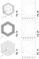
- Figures 1a show a hexagonal sense coil 1 with a linear turn distribution as known in the prior art.
- the sense coil 1 has a length of about 56 mm and a width of about 50 mm with a distance between the single turns of the coil of about 5 mm.
- Fig. 1b shows a qualitative illustration of the corresponding summed magnet field magnitude resulting from that hexagonal sense coil 1 for example when a stimulation signal including a step is applied.
- the horizontal axis shows the distance from centre of the sense coil 1 in m and the vertical axis shows the magnetic field strength in percent of the respective maximum value.
- the resulting absolute values of the magnetic field strength depend on various parameters of the particular application.
- Such a sensor arrangement 29 may for example be used in connection with a double D coil arrangement for generating the power transfer field as mentioned above.
- a coil arrangement generates a magnetic field having two poles, one in the centre of the first coil and one in the centre of the second coil.
- the sensor arrangement 29 is arranged above the coil arrangement such that the first column C1 of detection cells 30, 34 and 38 is positioned above the first pole of the power transfer field and such that the fourth column C4 of detection cells 33, 37 and 41 is positioned above the second pole of the power transfer field.
- the field lines of the power transfer field in the region between the second column C2 and the third column C3 generally run parallel to the planes of the detection cells.
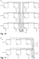
- the arrangement, the sizes and the spacing of the different elements of the sensor arrangement 59 such as the detection cells, the input and output leads are not to scale.
- all input leads 60, 61 and 62 and all output leads 66 and 67 are routed at the edge of the sensor arrangement 59 near the third column C3.
- the input and output leads of the detection cells of the first column C1 become longer than in a sensor arrangement where the input and output leads are routed through a gap between two central columns (or rows).
- the length of the input and output leads of the different detection cells does vary less than in the case where the input and output leads are routed along an edge or through a gap between two outer columns or rows.
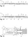
- Figure 12 shows a single layer sensor arrangement 69 with leads arranged one above the other in a side view.
- the sensor arrangement 69 is provided on a support structure such as a multilayer PCB 75 such that the detection cells 30, 31, 32, and 33 of the sensor arrangement 69 are provided on an upper surface of the PCB 75 or embedded in corresponding recesses respectively.
- a number of input and output leads 70, 71, 72, 73 are provided to connect the detection cells 30, 31, 32, and 33 to a current input and a current output respectively.
- a black dot in fig. 12 means that the corresponding line is perpendicular to the drawing plane.
- Figure 13 shows a double layer sensor arrangement 79 in a side view.
- the sensor arrangement 79 is provided on a support structure such as a multilayer PCB 85 and includes two layers of detection cells where each layer includes a matrix-like structure of detection cells.
- the first layer includes detection cells 30, 31, 32, and 33 provided on an upper surface of the PCB 85 or embedded in corresponding recesses respectively.
- the second layer includes detection cells 34, 35 and 36 provided on a lower surface of the PCB 85 or embedded in corresponding recesses respectively.
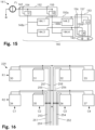
- the first detection cell 144.1 and the second detection cell 144.2 are part of the first row, while the third detection cell 144.3 and the fourth detection cell 144.4 are part of the second row.
- a first input lead 148a is connected to the input of the first detection cell 144.1, which is part of the first row and to the third detection cell 144.3, which is part of the second row.
- a second input lead 148b is connected to the second detection cell 144.2, which is part of the first row and to the fourth detection cell 144.4, which is part of the second row.
- the detection cells belonging to the first row are connected with their second terminals to a first output lead 150a.
- the detection cells belonging to the second row are connected with their second terminals to a second output lead 150b.
- the number of detection cells and the total number of input leads and output leads for this embodiment is four and therefore there are as many detection cells as input and output leads together.
- the sensor arrangement 140 comprises an output selection circuit 153 including a third switch Q3 and a fourth switch Q4.
- the third switch Q3 is connected between the first output lead 150a and the current output 143, which in this embodiment is connected to the electrical ground, and the fourth switch Q4 is connected between the second output lead 150b and the current output 143.
- the third switch Q3 or the fourth switch Q4 a row of the 2 x 2-sensor matrix can be selected.
- the input selection circuit 152 as well as the output selection circuit 153 include two control inputs 154, 155, 156, 157 that are connected to the control inputs of the respective switches Q1, Q2, Q3, and Q4. By means of these control inputs 154 - 157 the different switches Q1, Q2, Q3, and Q4 can be addressed and therewith the detection cells be selected.
- the stimulation unit 141 is configured to generate a rectangular current pulse, to stimulate an electrical oscillation in the parallel tank of the selected detection cell. It includes a current source and an internal switch, which is not shown in fig. 15 .
- An excited electrical oscillation in a selected detection cell yields to an oscillating voltage between the current input 142 and the current output 143 (ground), which can, for example, be sensed with an ADC connected with its terminals between the current input and ground.
- Figure 16 shows a schematic representation of another sensor arrangement 229 according to the invention.
- the sensor arrangement 229 includes 8 detection cells 30-37 arranged in a matrix-like structure with two rows R1 and R2 and four columns C1, C2, C3 and C4 where
- Each detection cell includes any sense coil as described above or known in the art, preferably a sense coil as described above.
- All input leads 251-258 enter the matrix-like structure between the two central columns C2 and C3, run in parallel until they are connected to their respective detection cell.
- the sensor arrangement 229 further includes just a single output lead 259 that interconnects the output terminal of all detection cells 30 - 37 and then leaves the matrix-like structure between the two central columns C2 and C3.
- the single output lead 259 is arranged in the centre of the input leads 251-258, in this case between the input leads 257 and 258.
- such a sensor arrangement usually does not include an output selection circuit to connect one or more of the output leads to the current output.
- the single output lead 259 is directly connected to the current output.
- a particular detection cell may be activated by connecting the input lead of that detection cell to the current input by means of the input selection circuit. And the output lead of that detection cell is permanently connected to the current output.
- all input leads 251-258 and the single output lead 259 are routed through the gap between the two central columns C2 and C3. And they are arranged such that the input and output leads of a particular detection cell are as near as possible arranged next to each other to minimise the area enclosed by the loop formed by the input and output lead of that cell. In the case of a double D arrangement, this can be, for example, in the middle between the two poles.
- the invention enables to create a sensor arrangement for a foreign object detection device with a minimized hardware effort and a minimized total length of the input and output leads as well as a sensor arrangement for a foreign object detection device that reduces the voltages induced in the input and output leads of the single detection cells by reducing the area that is enclosed by the input and output leads of the cells and that can be flowed through by the external magnetic field.
- the reduced voltages induced in the input and output leads minimizes interference effects and distortions of the foreign object detection by an external magnetic field such as the power transfer field of the wireless power transfer system.
Landscapes
- Engineering & Computer Science (AREA)
- Power Engineering (AREA)
- Computer Networks & Wireless Communication (AREA)
- Physics & Mathematics (AREA)
- Remote Sensing (AREA)
- Life Sciences & Earth Sciences (AREA)
- Geology (AREA)
- General Life Sciences & Earth Sciences (AREA)
- General Physics & Mathematics (AREA)
- Geophysics (AREA)
- Environmental & Geological Engineering (AREA)
- Electromagnetism (AREA)
- Geophysics And Detection Of Objects (AREA)
- Measurement Of Length, Angles, Or The Like Using Electric Or Magnetic Means (AREA)
Claims (9)
- Sensoranordnung (29, 59, 69, 79, 120, 140, 229) für eine Fremdkörperdetektionsvorrichtung (119) für ein drahtloses Energieübertragungssystem, umfassend:a) einen Stromeingang (135, 142) und einen Stromausgang (136, 143),b) eine Vielzahl von Detektionszellen (30 - 41, 144.1-144.4), die jeweils eine Erfassungsspule (1, 2, 3, 20, 22, 24) mit einer in einer Ebene spiralförmig gewickelten Wicklung mit einer Vielzahl von Windungen umfassen,c) wobei die Erfassungsspulen (1, 2, 3, 20, 22, 24) in einer oder mehreren Schichten angeordnet sind und wobei die Erfassungsspulen (1, 2, 3, 20, 22, 24) einer bestimmten Schicht in einer matrixartigen Struktur mit mehreren Zeilen und mehreren Spalten angeordnet sind,d) eine Vielzahl von Eingangsleitungen (50 - 53, 60 - 62, 127, 148a, 148b, 251 - 258) und eine oder mehrere Ausgangsleitungen (56, 57, 58, 66, 67, 128, 150a, 150b, 259), wobei jede Detektionszelle (30-41, 144.1-144.4) zwischen einer der Eingangsleitungen und einer Ausgangsleitung verbunden ist und wobei jede Detektionszelle mit einer anderen Kombination von Eingangs- und Ausgangsleitungen verbunden ist,e) eine Eingangsauswahlschaltung (125, 152), die geeignet ist, selektiv eine elektrische Verbindung zwischen dem Stromeingang (135, 142) und einer oder mehreren der Eingangsleitungen herzustellen,dadurch gekennzeichnet, dass
die Eingangsleitung (50 - 53, 60 - 62, 251 - 258) und die Ausgangsleitung (56, 57, 58, 66, 67, 259) mindestens einer Erfassungsspule (1, 2, 3, 20, 22, 24) durch die matrixartige Struktur, zu der die mindestens eine Erfassungsspule gehört, so nahe beieinander geführt wird, dass eine Fläche, die parallel zu erwähnter matrixartigen Struktur ist und die von erwähnten Eingangs- und Ausgangsleitungen eingeschlossen wird, reduziert wird. - Sensoranordnung (29, 59, 69, 79, 120, 140, 229) nach Anspruch 1, wobei die Eingangsleitungen (50 - 53, 251 - 258) und die Ausgangsleitungen (56, 57, 58, 259) jeder Erfassungsspule einer bestimmten Schicht durch eine Lücke zwischen zwei Spalten oder zwei Zeilen, vorzugsweise zwischen zwei mittleren Spalten oder zwei mittleren Zeilen, der matrixartigen Struktur geführt werden.
- Sensoranordnung (29, 59, 69, 79, 120, 140, 229) nach Anspruch 1 oder 2, wobei ein Abstand zwischen der Eingangsleitung (50 - 53, 60 - 62, 251 - 258) und der Ausgangsleitung (56, 57, 58, 66, 67, 259) erwähnter mindestens einer Erfassungsspule kleiner ist als ein Abstand zwischen zwei Zeilen oder zwei Spalten der matrixartigen Struktur.
- Sensoranordnung (29, 59, 69, 79, 120, 140, 229) nach einem der Ansprüche 1 bis 3, wobei die Eingangsleitung und die Ausgangsleitung erwähnter mindestens einer Erfassungsspule übereinander angeordnet sind.
- Sensoranordnung (29, 59, 69, 79, 120, 140, 229) nach einem der Ansprüche 1 bis 4, wobei die Eingangsleitung und die Ausgangsleitung der mindestens einen Erfassungsspule mindestens einmal verdrillt sind.
- Sensoranordnung (29, 59, 69, 79, 120, 140, 229) nach einem der vorherigen Ansprüche, umfassend eine Ausgangsauswahlschaltung (126, 153), die geeignet ist, um selektiv eine elektrische Verbindung zwischen einer oder mehreren der Ausgangsleitungen und dem Stromausgang (136, 143) herzustellen.
- Sensoranordnung (29, 59, 69, 79, 120, 140, 229) nach einem der vorherigen Ansprüche, wobei die Erfassungsspule (20, 24) der mindestens einen Detektionszelle eine rechteckige Form hat.
- Eine Fremdkörperdetektionsvorrichtung (119) für einen Primärteil eines drahtlosen Energieübertragungssystems zur Übertragung von Energie über einen Luftspalt zu einem nahegelegenen Empfänger, umfassend:a) eine Sensoranordnung (29, 59, 69, 79, 120, 140, 229) nach einem der Ansprüche 1 bis 7,b) eine Stimulationsschaltung (121) zur Erzeugung eines vorgegebenen Stimulationssignals, die mit einem Stromeingang (142) der Sensoranordnung (29, 59, 69, 79, 120, 140, 229) verbunden ist,c) eine Messeinheit (122), die geeignet ist, ein an den Stromeingang angelegtes elektrisches Signal zu erfassen, wobei die Messeinheit (122) einen Analog-DigitalWandler zur Erfassung von Abtastdaten umfasst, die das erfasste elektrische Signal darstellen, undd) eine Signalverarbeitungseinheit (123), die so konfiguriert ist, dass sie auf der Grundlage der von der Messeinheit erfassten Abtastdaten Reaktionszeitdaten einer ausgewählten Detektionszelle bestimmt.
- Ein Primärteil für ein drahtloses Energieübertragungssystem zur Übertragung von Energie über einen Luftspalt zu einem nahegelegenen Empfänger, der so ausgebildet ist, dass er in einer aktiven Fläche ein Magnetfeld mit einer Sendefrequenz erzeugt, wobei der Primärteil die Sensoranordnung (29, 59, 69, 79, 120, 140, 229) nach einem der Ansprüche 1 - 7 oder die Fremdkörperdetektionsvorrichtung (119) nach Anspruch 8 umfasst, wobei die Erfassungsspulen (1, 2, 3, 20, 22, 24) so angeordnet sind, dass eine durch die Erfassungsspulen definierte Erfassungsfläche die aktive Fläche zumindest teilweise und vorzugsweise vollständig abdeckt.
Priority Applications (1)
| Application Number | Priority Date | Filing Date | Title |
|---|---|---|---|
| EP23204735.7A EP4290739B1 (de) | 2021-10-25 | 2021-10-25 | Sensoranordnung für eine fremdkörperdetektionsvorrichtung |
Applications Claiming Priority (2)
| Application Number | Priority Date | Filing Date | Title |
|---|---|---|---|
| EP23204735.7A EP4290739B1 (de) | 2021-10-25 | 2021-10-25 | Sensoranordnung für eine fremdkörperdetektionsvorrichtung |
| EP21204530.6A EP4170860B1 (de) | 2021-10-25 | 2021-10-25 | Sensoranordnung für eine fremdkörperdetektionsvorrichtung |
Related Parent Applications (2)
| Application Number | Title | Priority Date | Filing Date |
|---|---|---|---|
| EP21204530.6A Division-Into EP4170860B1 (de) | 2021-10-25 | 2021-10-25 | Sensoranordnung für eine fremdkörperdetektionsvorrichtung |
| EP21204530.6A Division EP4170860B1 (de) | 2021-10-25 | 2021-10-25 | Sensoranordnung für eine fremdkörperdetektionsvorrichtung |
Publications (4)
| Publication Number | Publication Date |
|---|---|
| EP4290739A2 EP4290739A2 (de) | 2023-12-13 |
| EP4290739A3 EP4290739A3 (de) | 2024-02-21 |
| EP4290739C0 EP4290739C0 (de) | 2025-06-25 |
| EP4290739B1 true EP4290739B1 (de) | 2025-06-25 |
Family
ID=78598762
Family Applications (2)
| Application Number | Title | Priority Date | Filing Date |
|---|---|---|---|
| EP23204735.7A Active EP4290739B1 (de) | 2021-10-25 | 2021-10-25 | Sensoranordnung für eine fremdkörperdetektionsvorrichtung |
| EP21204530.6A Active EP4170860B1 (de) | 2021-10-25 | 2021-10-25 | Sensoranordnung für eine fremdkörperdetektionsvorrichtung |
Family Applications After (1)
| Application Number | Title | Priority Date | Filing Date |
|---|---|---|---|
| EP21204530.6A Active EP4170860B1 (de) | 2021-10-25 | 2021-10-25 | Sensoranordnung für eine fremdkörperdetektionsvorrichtung |
Country Status (3)
| Country | Link |
|---|---|
| US (2) | US12113370B2 (de) |
| EP (2) | EP4290739B1 (de) |
| CN (2) | CN116027437B (de) |
Family Cites Families (13)
| Publication number | Priority date | Publication date | Assignee | Title |
|---|---|---|---|---|
| DE102004047188B4 (de) * | 2004-09-29 | 2022-10-27 | Robert Bosch Gmbh | Vorrichtung zur Ortung metallischer Objekte |
| CN101776770B (zh) * | 2010-02-26 | 2012-07-25 | 重庆大学 | 一种电磁法勘查的发送接收一体化方法及装置 |
| US9404954B2 (en) * | 2012-10-19 | 2016-08-02 | Witricity Corporation | Foreign object detection in wireless energy transfer systems |
| DE102014207885A1 (de) * | 2014-04-28 | 2015-10-29 | Continental Automotive Gmbh | Fremdkörpererfassungsvorrichtung und Leistungs-Induktivladevorrichtung |
| CN105182428B (zh) * | 2015-07-29 | 2019-01-01 | 金华马卡科技有限公司 | 一种传感器、用于分析传感器的测量信号的方法以及检测物体的方法 |
| US10985465B2 (en) * | 2015-08-19 | 2021-04-20 | Nucurrent, Inc. | Multi-mode wireless antenna configurations |
| KR20190009639A (ko) * | 2017-07-19 | 2019-01-29 | 엘지전자 주식회사 | 이물질 검출 장치 및 무선 충전 시스템 |
| US20210215845A1 (en) * | 2018-05-18 | 2021-07-15 | Tdk Corporation | Foreign Object Detector, Wireless Power Transmission System Comprising a Foreign Object Detector and Method of Detecting a Foreign Object |
| US11002874B2 (en) * | 2018-12-21 | 2021-05-11 | Witricity Corporation | Foreign object detection circuit using mutual impedance sensing |
| EP3734801B1 (de) | 2019-05-03 | 2024-12-18 | Delta Electronics (Thailand) Public Co., Ltd. | Sensoranordnung für eine fremdkörperdetektionsvorrichtung |
| US11485494B2 (en) * | 2019-10-04 | 2022-11-01 | Northeastern University | Wireless charging of unmanned aerial vehicles |
| US20210265871A1 (en) * | 2020-02-20 | 2021-08-26 | Hyundai Motor Company | Object detection for wireless charging system |
| US11750041B2 (en) * | 2021-01-26 | 2023-09-05 | Witricity Corporation | Wire-wound structures for electromagnetic sensing of objects |
-
2021
- 2021-10-25 EP EP23204735.7A patent/EP4290739B1/de active Active
- 2021-10-25 EP EP21204530.6A patent/EP4170860B1/de active Active
-
2022
- 2022-10-25 US US18/049,613 patent/US12113370B2/en active Active
- 2022-10-25 CN CN202211310544.9A patent/CN116027437B/zh active Active
- 2022-10-25 CN CN202511091061.8A patent/CN120630312A/zh active Pending
-
2024
- 2024-09-10 US US18/829,318 patent/US20240429755A1/en active Pending
Also Published As
| Publication number | Publication date |
|---|---|
| EP4170860B1 (de) | 2024-06-12 |
| US20230131711A1 (en) | 2023-04-27 |
| US12113370B2 (en) | 2024-10-08 |
| CN116027437B (zh) | 2025-08-22 |
| EP4290739A2 (de) | 2023-12-13 |
| US20240429755A1 (en) | 2024-12-26 |
| CN116027437A (zh) | 2023-04-28 |
| EP4290739A3 (de) | 2024-02-21 |
| EP4290739C0 (de) | 2025-06-25 |
| EP4170860C0 (de) | 2024-06-12 |
| EP4170860A1 (de) | 2023-04-26 |
| CN120630312A (zh) | 2025-09-12 |
Similar Documents
| Publication | Publication Date | Title |
|---|---|---|
| US11594919B2 (en) | Sensor arrangement for a foreign object detection device | |
| CN105281442B (zh) | 送电装置以及受电装置 | |
| EP3016231B1 (de) | Kraftübertragungsvorrichtung, fahrzeug mit kraftübertragungsvorrichtung und drahtloses kraftübertragungssystem | |
| EP3920197B1 (de) | Spulenvorrichtung | |
| US20070181683A1 (en) | Wireless Sensing System Using Open-Circuit, Electrically-Conductive Spiral-Trace Sensor | |
| WO2009027674A1 (en) | Inductive power supply | |
| US11750041B2 (en) | Wire-wound structures for electromagnetic sensing of objects | |
| CA2328623C (en) | Arc detection sensor utilizing discrete inductors | |
| WO2023150546A1 (en) | Foreign object detection using hybrid inductive and capacitive sensing | |
| US12160121B2 (en) | Foreign object detection | |
| EP4290739B1 (de) | Sensoranordnung für eine fremdkörperdetektionsvorrichtung | |
| US20230361618A1 (en) | Wire-Wound Structures for Electromagnetic Sensing of Objects | |
| CN110518715A (zh) | 异物检测装置 | |
| CN210577962U (zh) | 异物检测装置 | |
| CN219154250U (zh) | 金属异物检测装置及无线充电发射端 | |
| CN109791214B (zh) | 用于在磁场中识别物体的网络和装置、方法和充电单元 | |
| JP3206983U (ja) | ワイヤレス給電システム | |
| KR20240097961A (ko) | 무선 충전 패드 내 이물질 검출 | |
| HK40037288A (en) | A sensor arrangement for a foreign object detection device | |
| CN120934210A (zh) | 线圈组件、异物检测系统、无线充电系统及车辆 | |
| CN116746027A (zh) | 用于对物体进行电磁感测的绕线结构 | |
| WO2018215060A1 (en) | Foreign object detector, foreign object detection system, use of a foreign object detector, and method of detecting a foreign object |
Legal Events
| Date | Code | Title | Description |
|---|---|---|---|
| PUAI | Public reference made under article 153(3) epc to a published international application that has entered the european phase |
Free format text: ORIGINAL CODE: 0009012 |
|
| STAA | Information on the status of an ep patent application or granted ep patent |
Free format text: STATUS: THE APPLICATION HAS BEEN PUBLISHED |
|
| AC | Divisional application: reference to earlier application |
Ref document number: 4170860 Country of ref document: EP Kind code of ref document: P |
|
| AK | Designated contracting states |
Kind code of ref document: A2 Designated state(s): AL AT BE BG CH CY CZ DE DK EE ES FI FR GB GR HR HU IE IS IT LI LT LU LV MC MK MT NL NO PL PT RO RS SE SI SK SM TR |
|
| REG | Reference to a national code |
Ref country code: DE Ref legal event code: R079 Free format text: PREVIOUS MAIN CLASS: H02J0050600000 Ipc: H02J0050000000 Ref document number: 602021033134 Country of ref document: DE |
|
| PUAL | Search report despatched |
Free format text: ORIGINAL CODE: 0009013 |
|
| AK | Designated contracting states |
Kind code of ref document: A3 Designated state(s): AL AT BE BG CH CY CZ DE DK EE ES FI FR GB GR HR HU IE IS IT LI LT LU LV MC MK MT NL NO PL PT RO RS SE SI SK SM TR |
|
| RIC1 | Information provided on ipc code assigned before grant |
Ipc: H02J 50/60 20160101ALI20240116BHEP Ipc: H02J 50/40 20160101ALI20240116BHEP Ipc: H02J 50/00 20160101AFI20240116BHEP |
|
| STAA | Information on the status of an ep patent application or granted ep patent |
Free format text: STATUS: REQUEST FOR EXAMINATION WAS MADE |
|
| 17P | Request for examination filed |
Effective date: 20240820 |
|
| RBV | Designated contracting states (corrected) |
Designated state(s): AL AT BE BG CH CY CZ DE DK EE ES FI FR GB GR HR HU IE IS IT LI LT LU LV MC MK MT NL NO PL PT RO RS SE SI SK SM TR |
|
| GRAP | Despatch of communication of intention to grant a patent |
Free format text: ORIGINAL CODE: EPIDOSNIGR1 |
|
| STAA | Information on the status of an ep patent application or granted ep patent |
Free format text: STATUS: GRANT OF PATENT IS INTENDED |
|
| INTG | Intention to grant announced |
Effective date: 20250121 |
|
| RAP3 | Party data changed (applicant data changed or rights of an application transferred) |
Owner name: DELTA ELECTRONICS (THAILAND) PUBLIC CO., LTD. |
|
| GRAS | Grant fee paid |
Free format text: ORIGINAL CODE: EPIDOSNIGR3 |
|
| GRAA | (expected) grant |
Free format text: ORIGINAL CODE: 0009210 |
|
| STAA | Information on the status of an ep patent application or granted ep patent |
Free format text: STATUS: THE PATENT HAS BEEN GRANTED |
|
| AC | Divisional application: reference to earlier application |
Ref document number: 4170860 Country of ref document: EP Kind code of ref document: P |
|
| AK | Designated contracting states |
Kind code of ref document: B1 Designated state(s): AL AT BE BG CH CY CZ DE DK EE ES FI FR GB GR HR HU IE IS IT LI LT LU LV MC MK MT NL NO PL PT RO RS SE SI SK SM TR |
|
| REG | Reference to a national code |
Ref country code: GB Ref legal event code: FG4D |
|
| REG | Reference to a national code |
Ref country code: CH Ref legal event code: EP |
|
| REG | Reference to a national code |
Ref country code: CH Ref legal event code: EP |
|
| REG | Reference to a national code |
Ref country code: IE Ref legal event code: FG4D |
|
| REG | Reference to a national code |
Ref country code: DE Ref legal event code: R096 Ref document number: 602021033134 Country of ref document: DE |
|
| U01 | Request for unitary effect filed |
Effective date: 20250708 |
|
| U07 | Unitary effect registered |
Designated state(s): AT BE BG DE DK EE FI FR IT LT LU LV MT NL PT RO SE SI Effective date: 20250714 |
|
| PG25 | Lapsed in a contracting state [announced via postgrant information from national office to epo] |
Ref country code: NO Free format text: LAPSE BECAUSE OF FAILURE TO SUBMIT A TRANSLATION OF THE DESCRIPTION OR TO PAY THE FEE WITHIN THE PRESCRIBED TIME-LIMIT Effective date: 20250925 Ref country code: GR Free format text: LAPSE BECAUSE OF FAILURE TO SUBMIT A TRANSLATION OF THE DESCRIPTION OR TO PAY THE FEE WITHIN THE PRESCRIBED TIME-LIMIT Effective date: 20250926 |
|
| PG25 | Lapsed in a contracting state [announced via postgrant information from national office to epo] |
Ref country code: HR Free format text: LAPSE BECAUSE OF FAILURE TO SUBMIT A TRANSLATION OF THE DESCRIPTION OR TO PAY THE FEE WITHIN THE PRESCRIBED TIME-LIMIT Effective date: 20250625 |
|
| PG25 | Lapsed in a contracting state [announced via postgrant information from national office to epo] |
Ref country code: RS Free format text: LAPSE BECAUSE OF FAILURE TO SUBMIT A TRANSLATION OF THE DESCRIPTION OR TO PAY THE FEE WITHIN THE PRESCRIBED TIME-LIMIT Effective date: 20250925 |
|
| REG | Reference to a national code |
Ref country code: CH Ref legal event code: U11 Free format text: ST27 STATUS EVENT CODE: U-0-0-U10-U11 (AS PROVIDED BY THE NATIONAL OFFICE) Effective date: 20251101 |
|
| U20 | Renewal fee for the european patent with unitary effect paid |
Year of fee payment: 5 Effective date: 20251028 |
|
| PG25 | Lapsed in a contracting state [announced via postgrant information from national office to epo] |
Ref country code: IS Free format text: LAPSE BECAUSE OF FAILURE TO SUBMIT A TRANSLATION OF THE DESCRIPTION OR TO PAY THE FEE WITHIN THE PRESCRIBED TIME-LIMIT Effective date: 20251025 |
|
| PGFP | Annual fee paid to national office [announced via postgrant information from national office to epo] |
Ref country code: GB Payment date: 20251022 Year of fee payment: 5 |
|
| PG25 | Lapsed in a contracting state [announced via postgrant information from national office to epo] |
Ref country code: SM Free format text: LAPSE BECAUSE OF FAILURE TO SUBMIT A TRANSLATION OF THE DESCRIPTION OR TO PAY THE FEE WITHIN THE PRESCRIBED TIME-LIMIT Effective date: 20250625 |
|
| PGFP | Annual fee paid to national office [announced via postgrant information from national office to epo] |
Ref country code: CH Payment date: 20251101 Year of fee payment: 5 |
|
| PG25 | Lapsed in a contracting state [announced via postgrant information from national office to epo] |
Ref country code: CZ Free format text: LAPSE BECAUSE OF FAILURE TO SUBMIT A TRANSLATION OF THE DESCRIPTION OR TO PAY THE FEE WITHIN THE PRESCRIBED TIME-LIMIT Effective date: 20250625 |
|
| PG25 | Lapsed in a contracting state [announced via postgrant information from national office to epo] |
Ref country code: PL Free format text: LAPSE BECAUSE OF FAILURE TO SUBMIT A TRANSLATION OF THE DESCRIPTION OR TO PAY THE FEE WITHIN THE PRESCRIBED TIME-LIMIT Effective date: 20250625 |
|
| PG25 | Lapsed in a contracting state [announced via postgrant information from national office to epo] |
Ref country code: SK Free format text: LAPSE BECAUSE OF FAILURE TO SUBMIT A TRANSLATION OF THE DESCRIPTION OR TO PAY THE FEE WITHIN THE PRESCRIBED TIME-LIMIT Effective date: 20250625 |
|
| PG25 | Lapsed in a contracting state [announced via postgrant information from national office to epo] |
Ref country code: ES Free format text: LAPSE BECAUSE OF FAILURE TO SUBMIT A TRANSLATION OF THE DESCRIPTION OR TO PAY THE FEE WITHIN THE PRESCRIBED TIME-LIMIT Effective date: 20250625 |