EP3893281B1 - Device with array of light-emitting and/or light-receiving diodes - Google Patents
Device with array of light-emitting and/or light-receiving diodes Download PDFInfo
- Publication number
- EP3893281B1 EP3893281B1 EP21166778.7A EP21166778A EP3893281B1 EP 3893281 B1 EP3893281 B1 EP 3893281B1 EP 21166778 A EP21166778 A EP 21166778A EP 3893281 B1 EP3893281 B1 EP 3893281B1
- Authority
- EP
- European Patent Office
- Prior art keywords
- layer
- trenches
- stack
- diodes
- electrically conductive
- Prior art date
- Legal status (The legal status is an assumption and is not a legal conclusion. Google has not performed a legal analysis and makes no representation as to the accuracy of the status listed.)
- Active
Links
- 239000004065 semiconductor Substances 0.000 claims description 62
- 239000000758 substrate Substances 0.000 claims description 52
- 238000005530 etching Methods 0.000 claims description 46
- 238000004519 manufacturing process Methods 0.000 claims description 41
- 239000004020 conductor Substances 0.000 claims description 35
- 238000000034 method Methods 0.000 claims description 21
- 238000000151 deposition Methods 0.000 claims description 16
- 230000008021 deposition Effects 0.000 claims description 15
- 238000000407 epitaxy Methods 0.000 claims description 3
- 239000010410 layer Substances 0.000 description 250
- 239000011159 matrix material Substances 0.000 description 48
- 239000000463 material Substances 0.000 description 28
- 230000003287 optical effect Effects 0.000 description 11
- 230000008569 process Effects 0.000 description 8
- 238000002955 isolation Methods 0.000 description 7
- 229910052782 aluminium Inorganic materials 0.000 description 5
- 238000011049 filling Methods 0.000 description 5
- 238000005286 illumination Methods 0.000 description 5
- 239000000370 acceptor Substances 0.000 description 4
- XAGFODPZIPBFFR-UHFFFAOYSA-N aluminium Chemical compound [Al] XAGFODPZIPBFFR-UHFFFAOYSA-N 0.000 description 4
- 238000003491 array Methods 0.000 description 4
- 229910052802 copper Inorganic materials 0.000 description 4
- 239000010949 copper Substances 0.000 description 4
- 238000001020 plasma etching Methods 0.000 description 4
- 238000004088 simulation Methods 0.000 description 4
- RYGMFSIKBFXOCR-UHFFFAOYSA-N Copper Chemical compound [Cu] RYGMFSIKBFXOCR-UHFFFAOYSA-N 0.000 description 3
- 229910004298 SiO 2 Inorganic materials 0.000 description 3
- 230000007423 decrease Effects 0.000 description 3
- 239000003989 dielectric material Substances 0.000 description 3
- 238000009396 hybridization Methods 0.000 description 3
- 238000004377 microelectronic Methods 0.000 description 3
- 229910052710 silicon Inorganic materials 0.000 description 3
- 239000010703 silicon Substances 0.000 description 3
- 229910002704 AlGaN Inorganic materials 0.000 description 2
- 241001080024 Telles Species 0.000 description 2
- HCHKCACWOHOZIP-UHFFFAOYSA-N Zinc Chemical compound [Zn] HCHKCACWOHOZIP-UHFFFAOYSA-N 0.000 description 2
- 238000000231 atomic layer deposition Methods 0.000 description 2
- 230000004888 barrier function Effects 0.000 description 2
- 230000000903 blocking effect Effects 0.000 description 2
- 230000007547 defect Effects 0.000 description 2
- 238000001312 dry etching Methods 0.000 description 2
- 238000004070 electrodeposition Methods 0.000 description 2
- 238000000605 extraction Methods 0.000 description 2
- 238000000227 grinding Methods 0.000 description 2
- APFVFJFRJDLVQX-UHFFFAOYSA-N indium atom Chemical compound [In] APFVFJFRJDLVQX-UHFFFAOYSA-N 0.000 description 2
- 238000005304 joining Methods 0.000 description 2
- 238000001459 lithography Methods 0.000 description 2
- 108091008695 photoreceptors Proteins 0.000 description 2
- 230000005855 radiation Effects 0.000 description 2
- 229910052594 sapphire Inorganic materials 0.000 description 2
- 239000010980 sapphire Substances 0.000 description 2
- 229910052709 silver Inorganic materials 0.000 description 2
- 239000011701 zinc Substances 0.000 description 2
- 229910018072 Al 2 O 3 Inorganic materials 0.000 description 1
- 229910000980 Aluminium gallium arsenide Inorganic materials 0.000 description 1
- OKTJSMMVPCPJKN-UHFFFAOYSA-N Carbon Chemical compound [C] OKTJSMMVPCPJKN-UHFFFAOYSA-N 0.000 description 1
- QPLDLSVMHZLSFG-UHFFFAOYSA-N Copper oxide Chemical compound [Cu]=O QPLDLSVMHZLSFG-UHFFFAOYSA-N 0.000 description 1
- 239000005751 Copper oxide Substances 0.000 description 1
- 229910001218 Gallium arsenide Inorganic materials 0.000 description 1
- 229910000530 Gallium indium arsenide Inorganic materials 0.000 description 1
- 229910007637 SnAg Inorganic materials 0.000 description 1
- RTAQQCXQSZGOHL-UHFFFAOYSA-N Titanium Chemical compound [Ti] RTAQQCXQSZGOHL-UHFFFAOYSA-N 0.000 description 1
- 230000008901 benefit Effects 0.000 description 1
- 229910052799 carbon Inorganic materials 0.000 description 1
- 238000005229 chemical vapour deposition Methods 0.000 description 1
- 229910000431 copper oxide Inorganic materials 0.000 description 1
- 230000008878 coupling Effects 0.000 description 1
- 238000010168 coupling process Methods 0.000 description 1
- 238000005859 coupling reaction Methods 0.000 description 1
- 229960004643 cupric oxide Drugs 0.000 description 1
- 238000005520 cutting process Methods 0.000 description 1
- AJNVQOSZGJRYEI-UHFFFAOYSA-N digallium;oxygen(2-) Chemical compound [O-2].[O-2].[O-2].[Ga+3].[Ga+3] AJNVQOSZGJRYEI-UHFFFAOYSA-N 0.000 description 1
- 239000006185 dispersion Substances 0.000 description 1
- 238000010292 electrical insulation Methods 0.000 description 1
- 238000005516 engineering process Methods 0.000 description 1
- 229910000743 fusible alloy Inorganic materials 0.000 description 1
- 229910001195 gallium oxide Inorganic materials 0.000 description 1
- 239000011521 glass Substances 0.000 description 1
- 229910052737 gold Inorganic materials 0.000 description 1
- 230000009643 growth defect Effects 0.000 description 1
- 238000011065 in-situ storage Methods 0.000 description 1
- 229910052738 indium Inorganic materials 0.000 description 1
- 229910003437 indium oxide Inorganic materials 0.000 description 1
- 230000007246 mechanism Effects 0.000 description 1
- 239000007769 metal material Substances 0.000 description 1
- 230000010070 molecular adhesion Effects 0.000 description 1
- TWNQGVIAIRXVLR-UHFFFAOYSA-N oxo(oxoalumanyloxy)alumane Chemical compound O=[Al]O[Al]=O TWNQGVIAIRXVLR-UHFFFAOYSA-N 0.000 description 1
- 238000002161 passivation Methods 0.000 description 1
- 239000004038 photonic crystal Substances 0.000 description 1
- 238000000623 plasma-assisted chemical vapour deposition Methods 0.000 description 1
- 230000009467 reduction Effects 0.000 description 1
- 230000000717 retained effect Effects 0.000 description 1
- 238000000926 separation method Methods 0.000 description 1
- 229910021332 silicide Inorganic materials 0.000 description 1
- FVBUAEGBCNSCDD-UHFFFAOYSA-N silicide(4-) Chemical compound [Si-4] FVBUAEGBCNSCDD-UHFFFAOYSA-N 0.000 description 1
- 239000004332 silver Substances 0.000 description 1
- 239000002356 single layer Substances 0.000 description 1
- 229910000679 solder Inorganic materials 0.000 description 1
- 239000007787 solid Substances 0.000 description 1
- 239000000126 substance Substances 0.000 description 1
- XOLBLPGZBRYERU-UHFFFAOYSA-N tin dioxide Chemical compound O=[Sn]=O XOLBLPGZBRYERU-UHFFFAOYSA-N 0.000 description 1
- 229910001887 tin oxide Inorganic materials 0.000 description 1
- 239000010936 titanium Substances 0.000 description 1
- 229910052719 titanium Inorganic materials 0.000 description 1
- 238000004627 transmission electron microscopy Methods 0.000 description 1
- 229910052725 zinc Inorganic materials 0.000 description 1
- XLOMVQKBTHCTTD-UHFFFAOYSA-N zinc oxide Inorganic materials [Zn]=O XLOMVQKBTHCTTD-UHFFFAOYSA-N 0.000 description 1
Images


Classifications
-
- H—ELECTRICITY
- H01—ELECTRIC ELEMENTS
- H01L—SEMICONDUCTOR DEVICES NOT COVERED BY CLASS H10
- H01L33/00—Semiconductor devices with at least one potential-jump barrier or surface barrier specially adapted for light emission; Processes or apparatus specially adapted for the manufacture or treatment thereof or of parts thereof; Details thereof
- H01L33/36—Semiconductor devices with at least one potential-jump barrier or surface barrier specially adapted for light emission; Processes or apparatus specially adapted for the manufacture or treatment thereof or of parts thereof; Details thereof characterised by the electrodes
- H01L33/38—Semiconductor devices with at least one potential-jump barrier or surface barrier specially adapted for light emission; Processes or apparatus specially adapted for the manufacture or treatment thereof or of parts thereof; Details thereof characterised by the electrodes with a particular shape
- H01L33/382—Semiconductor devices with at least one potential-jump barrier or surface barrier specially adapted for light emission; Processes or apparatus specially adapted for the manufacture or treatment thereof or of parts thereof; Details thereof characterised by the electrodes with a particular shape the electrode extending partially in or entirely through the semiconductor body
-
- H—ELECTRICITY
- H01—ELECTRIC ELEMENTS
- H01L—SEMICONDUCTOR DEVICES NOT COVERED BY CLASS H10
- H01L33/00—Semiconductor devices with at least one potential-jump barrier or surface barrier specially adapted for light emission; Processes or apparatus specially adapted for the manufacture or treatment thereof or of parts thereof; Details thereof
- H01L33/48—Semiconductor devices with at least one potential-jump barrier or surface barrier specially adapted for light emission; Processes or apparatus specially adapted for the manufacture or treatment thereof or of parts thereof; Details thereof characterised by the semiconductor body packages
- H01L33/62—Arrangements for conducting electric current to or from the semiconductor body, e.g. lead-frames, wire-bonds or solder balls
-
- H—ELECTRICITY
- H01—ELECTRIC ELEMENTS
- H01L—SEMICONDUCTOR DEVICES NOT COVERED BY CLASS H10
- H01L31/00—Semiconductor devices sensitive to infrared radiation, light, electromagnetic radiation of shorter wavelength or corpuscular radiation and specially adapted either for the conversion of the energy of such radiation into electrical energy or for the control of electrical energy by such radiation; Processes or apparatus specially adapted for the manufacture or treatment thereof or of parts thereof; Details thereof
- H01L31/12—Semiconductor devices sensitive to infrared radiation, light, electromagnetic radiation of shorter wavelength or corpuscular radiation and specially adapted either for the conversion of the energy of such radiation into electrical energy or for the control of electrical energy by such radiation; Processes or apparatus specially adapted for the manufacture or treatment thereof or of parts thereof; Details thereof structurally associated with, e.g. formed in or on a common substrate with, one or more electric light sources, e.g. electroluminescent light sources, and electrically or optically coupled thereto
- H01L31/125—Composite devices with photosensitive elements and electroluminescent elements within one single body
-
- H—ELECTRICITY
- H01—ELECTRIC ELEMENTS
- H01L—SEMICONDUCTOR DEVICES NOT COVERED BY CLASS H10
- H01L25/00—Assemblies consisting of a plurality of individual semiconductor or other solid state devices ; Multistep manufacturing processes thereof
- H01L25/16—Assemblies consisting of a plurality of individual semiconductor or other solid state devices ; Multistep manufacturing processes thereof the devices being of types provided for in two or more different main groups of groups H01L27/00 - H01L33/00, or in a single subclass of H10K, H10N, e.g. forming hybrid circuits
- H01L25/167—Assemblies consisting of a plurality of individual semiconductor or other solid state devices ; Multistep manufacturing processes thereof the devices being of types provided for in two or more different main groups of groups H01L27/00 - H01L33/00, or in a single subclass of H10K, H10N, e.g. forming hybrid circuits comprising optoelectronic devices, e.g. LED, photodiodes
-
- H—ELECTRICITY
- H01—ELECTRIC ELEMENTS
- H01L—SEMICONDUCTOR DEVICES NOT COVERED BY CLASS H10
- H01L27/00—Devices consisting of a plurality of semiconductor or other solid-state components formed in or on a common substrate
- H01L27/14—Devices consisting of a plurality of semiconductor or other solid-state components formed in or on a common substrate including semiconductor components sensitive to infrared radiation, light, electromagnetic radiation of shorter wavelength or corpuscular radiation and specially adapted either for the conversion of the energy of such radiation into electrical energy or for the control of electrical energy by such radiation
- H01L27/144—Devices controlled by radiation
- H01L27/146—Imager structures
- H01L27/14601—Structural or functional details thereof
- H01L27/14603—Special geometry or disposition of pixel-elements, address-lines or gate-electrodes
- H01L27/14605—Structural or functional details relating to the position of the pixel elements, e.g. smaller pixel elements in the center of the imager compared to pixel elements at the periphery
-
- H—ELECTRICITY
- H01—ELECTRIC ELEMENTS
- H01L—SEMICONDUCTOR DEVICES NOT COVERED BY CLASS H10
- H01L27/00—Devices consisting of a plurality of semiconductor or other solid-state components formed in or on a common substrate
- H01L27/14—Devices consisting of a plurality of semiconductor or other solid-state components formed in or on a common substrate including semiconductor components sensitive to infrared radiation, light, electromagnetic radiation of shorter wavelength or corpuscular radiation and specially adapted either for the conversion of the energy of such radiation into electrical energy or for the control of electrical energy by such radiation
- H01L27/144—Devices controlled by radiation
- H01L27/146—Imager structures
- H01L27/14601—Structural or functional details thereof
- H01L27/14634—Assemblies, i.e. Hybrid structures
-
- H—ELECTRICITY
- H01—ELECTRIC ELEMENTS
- H01L—SEMICONDUCTOR DEVICES NOT COVERED BY CLASS H10
- H01L27/00—Devices consisting of a plurality of semiconductor or other solid-state components formed in or on a common substrate
- H01L27/14—Devices consisting of a plurality of semiconductor or other solid-state components formed in or on a common substrate including semiconductor components sensitive to infrared radiation, light, electromagnetic radiation of shorter wavelength or corpuscular radiation and specially adapted either for the conversion of the energy of such radiation into electrical energy or for the control of electrical energy by such radiation
- H01L27/144—Devices controlled by radiation
- H01L27/146—Imager structures
- H01L27/14601—Structural or functional details thereof
- H01L27/14636—Interconnect structures
-
- H—ELECTRICITY
- H01—ELECTRIC ELEMENTS
- H01L—SEMICONDUCTOR DEVICES NOT COVERED BY CLASS H10
- H01L27/00—Devices consisting of a plurality of semiconductor or other solid-state components formed in or on a common substrate
- H01L27/14—Devices consisting of a plurality of semiconductor or other solid-state components formed in or on a common substrate including semiconductor components sensitive to infrared radiation, light, electromagnetic radiation of shorter wavelength or corpuscular radiation and specially adapted either for the conversion of the energy of such radiation into electrical energy or for the control of electrical energy by such radiation
- H01L27/144—Devices controlled by radiation
- H01L27/146—Imager structures
- H01L27/14665—Imagers using a photoconductor layer
-
- H—ELECTRICITY
- H01—ELECTRIC ELEMENTS
- H01L—SEMICONDUCTOR DEVICES NOT COVERED BY CLASS H10
- H01L27/00—Devices consisting of a plurality of semiconductor or other solid-state components formed in or on a common substrate
- H01L27/14—Devices consisting of a plurality of semiconductor or other solid-state components formed in or on a common substrate including semiconductor components sensitive to infrared radiation, light, electromagnetic radiation of shorter wavelength or corpuscular radiation and specially adapted either for the conversion of the energy of such radiation into electrical energy or for the control of electrical energy by such radiation
- H01L27/144—Devices controlled by radiation
- H01L27/146—Imager structures
- H01L27/14683—Processes or apparatus peculiar to the manufacture or treatment of these devices or parts thereof
- H01L27/14692—Thin film technologies, e.g. amorphous, poly, micro- or nanocrystalline silicon
-
- H—ELECTRICITY
- H01—ELECTRIC ELEMENTS
- H01L—SEMICONDUCTOR DEVICES NOT COVERED BY CLASS H10
- H01L27/00—Devices consisting of a plurality of semiconductor or other solid-state components formed in or on a common substrate
- H01L27/15—Devices consisting of a plurality of semiconductor or other solid-state components formed in or on a common substrate including semiconductor components with at least one potential-jump barrier or surface barrier specially adapted for light emission
- H01L27/153—Devices consisting of a plurality of semiconductor or other solid-state components formed in or on a common substrate including semiconductor components with at least one potential-jump barrier or surface barrier specially adapted for light emission in a repetitive configuration, e.g. LED bars
- H01L27/156—Devices consisting of a plurality of semiconductor or other solid-state components formed in or on a common substrate including semiconductor components with at least one potential-jump barrier or surface barrier specially adapted for light emission in a repetitive configuration, e.g. LED bars two-dimensional arrays
-
- H—ELECTRICITY
- H01—ELECTRIC ELEMENTS
- H01L—SEMICONDUCTOR DEVICES NOT COVERED BY CLASS H10
- H01L31/00—Semiconductor devices sensitive to infrared radiation, light, electromagnetic radiation of shorter wavelength or corpuscular radiation and specially adapted either for the conversion of the energy of such radiation into electrical energy or for the control of electrical energy by such radiation; Processes or apparatus specially adapted for the manufacture or treatment thereof or of parts thereof; Details thereof
- H01L31/02—Details
- H01L31/02002—Arrangements for conducting electric current to or from the device in operations
- H01L31/02005—Arrangements for conducting electric current to or from the device in operations for device characterised by at least one potential jump barrier or surface barrier
-
- H—ELECTRICITY
- H01—ELECTRIC ELEMENTS
- H01L—SEMICONDUCTOR DEVICES NOT COVERED BY CLASS H10
- H01L31/00—Semiconductor devices sensitive to infrared radiation, light, electromagnetic radiation of shorter wavelength or corpuscular radiation and specially adapted either for the conversion of the energy of such radiation into electrical energy or for the control of electrical energy by such radiation; Processes or apparatus specially adapted for the manufacture or treatment thereof or of parts thereof; Details thereof
- H01L31/02—Details
- H01L31/02016—Circuit arrangements of general character for the devices
- H01L31/02019—Circuit arrangements of general character for the devices for devices characterised by at least one potential jump barrier or surface barrier
- H01L31/02024—Position sensitive and lateral effect photodetectors; Quadrant photodiodes
-
- H—ELECTRICITY
- H01—ELECTRIC ELEMENTS
- H01L—SEMICONDUCTOR DEVICES NOT COVERED BY CLASS H10
- H01L31/00—Semiconductor devices sensitive to infrared radiation, light, electromagnetic radiation of shorter wavelength or corpuscular radiation and specially adapted either for the conversion of the energy of such radiation into electrical energy or for the control of electrical energy by such radiation; Processes or apparatus specially adapted for the manufacture or treatment thereof or of parts thereof; Details thereof
- H01L31/08—Semiconductor devices sensitive to infrared radiation, light, electromagnetic radiation of shorter wavelength or corpuscular radiation and specially adapted either for the conversion of the energy of such radiation into electrical energy or for the control of electrical energy by such radiation; Processes or apparatus specially adapted for the manufacture or treatment thereof or of parts thereof; Details thereof in which radiation controls flow of current through the device, e.g. photoresistors
- H01L31/10—Semiconductor devices sensitive to infrared radiation, light, electromagnetic radiation of shorter wavelength or corpuscular radiation and specially adapted either for the conversion of the energy of such radiation into electrical energy or for the control of electrical energy by such radiation; Processes or apparatus specially adapted for the manufacture or treatment thereof or of parts thereof; Details thereof in which radiation controls flow of current through the device, e.g. photoresistors characterised by at least one potential-jump barrier or surface barrier, e.g. phototransistors
- H01L31/101—Devices sensitive to infrared, visible or ultraviolet radiation
-
- H—ELECTRICITY
- H01—ELECTRIC ELEMENTS
- H01L—SEMICONDUCTOR DEVICES NOT COVERED BY CLASS H10
- H01L31/00—Semiconductor devices sensitive to infrared radiation, light, electromagnetic radiation of shorter wavelength or corpuscular radiation and specially adapted either for the conversion of the energy of such radiation into electrical energy or for the control of electrical energy by such radiation; Processes or apparatus specially adapted for the manufacture or treatment thereof or of parts thereof; Details thereof
- H01L31/18—Processes or apparatus specially adapted for the manufacture or treatment of these devices or of parts thereof
- H01L31/1876—Particular processes or apparatus for batch treatment of the devices
-
- H—ELECTRICITY
- H01—ELECTRIC ELEMENTS
- H01L—SEMICONDUCTOR DEVICES NOT COVERED BY CLASS H10
- H01L33/00—Semiconductor devices with at least one potential-jump barrier or surface barrier specially adapted for light emission; Processes or apparatus specially adapted for the manufacture or treatment thereof or of parts thereof; Details thereof
- H01L33/005—Processes
- H01L33/0093—Wafer bonding; Removal of the growth substrate
-
- H—ELECTRICITY
- H01—ELECTRIC ELEMENTS
- H01L—SEMICONDUCTOR DEVICES NOT COVERED BY CLASS H10
- H01L33/00—Semiconductor devices with at least one potential-jump barrier or surface barrier specially adapted for light emission; Processes or apparatus specially adapted for the manufacture or treatment thereof or of parts thereof; Details thereof
- H01L33/005—Processes
- H01L33/0095—Post-treatment of devices, e.g. annealing, recrystallisation or short-circuit elimination
-
- H—ELECTRICITY
- H01—ELECTRIC ELEMENTS
- H01L—SEMICONDUCTOR DEVICES NOT COVERED BY CLASS H10
- H01L33/00—Semiconductor devices with at least one potential-jump barrier or surface barrier specially adapted for light emission; Processes or apparatus specially adapted for the manufacture or treatment thereof or of parts thereof; Details thereof
- H01L33/36—Semiconductor devices with at least one potential-jump barrier or surface barrier specially adapted for light emission; Processes or apparatus specially adapted for the manufacture or treatment thereof or of parts thereof; Details thereof characterised by the electrodes
- H01L33/38—Semiconductor devices with at least one potential-jump barrier or surface barrier specially adapted for light emission; Processes or apparatus specially adapted for the manufacture or treatment thereof or of parts thereof; Details thereof characterised by the electrodes with a particular shape
- H01L33/385—Semiconductor devices with at least one potential-jump barrier or surface barrier specially adapted for light emission; Processes or apparatus specially adapted for the manufacture or treatment thereof or of parts thereof; Details thereof characterised by the electrodes with a particular shape the electrode extending at least partially onto a side surface of the semiconductor body
Definitions
- a device with photo-emitting and/or photo-receiving diodes it is often advantageous to increase the resolution of the device, that is to say to increase the number of active cells, or pixels, per unit area. of the device.
- This increase in resolution involves reducing the unit size of the pixels while trying not to increase crosstalk (or "cross-talk"), that is to say the optical interference occurring between adjacent pixels and to minimize the decrease in performance of diodes generally observed on small pixels.
- the document FR 3 042 913 describes a technology for manufacturing photo-emitting and/or photo-receiving diode arrays in which the pixels are produced in a self-aligned manner using a single level of lithography making it possible both to physically separate the different diodes by creating mesa structures, and to make the electrical contact of the N-doped portion of each diode only by contact with the lateral flanks of this portion.
- each photo-emitting and/or photo-receiving diode is defined by the size of the fabricated mesa structure and the etched trenches cross the entire thickness of epitaxial semiconductor to form the diodes, up to the substrate.
- This etching defining the pixels causes defects in the semiconductor material because it damages all the side flanks of the mesa structures, thus causing a decrease in performance, in particular the external quantum efficiency (EQE), of the photo-emitting diodes and/or photoreceptors when their size decreases.
- EQE external quantum efficiency
- the method proposed in the document FR 3 042 913 does not allow the production of a matrix of photo-emitting and/or photo-receiving diodes with a variable diode density within the matrix while maintaining uniform performance over the entire surface of the matrix.
- the document US 2019/0355786 A1 discloses a device comprising an array of clustered pixels in which a connection to a first semiconductor layer common to all pixels is formed in a trench formed at least through a second semiconductor layer. Each photo-diode comprises electrodes arranged on the same surface of said device.
- the device according to the document US 2019/0355786 A1 further comprises optical isolation trenches between groups of pixels, said optical isolation trenches being filled with a reflective material. Said reflective material and the connection to a first semiconductor layer can be formed from the same conductive material.
- Diode array devices are also known from documents WO 2017/068029 A1 , US 2016/043119 A1 , US 10 204 950 B1 , EP 3 624 192 A1 , US 2019/043901 A1 and WO 2016/060676 A1 .
- An object of the present invention is to provide a device with a matrix of photo-emitting and/or photo-receiving diodes, the structure of which allows production by limiting the damage to the side flanks of the diodes, and which is compatible with a density of diodes variable within the matrix.
- the portions of the second layer of diodes formed in said region of the stack form a continuous semiconductor portion which is not crossed by the first and second trenches.
- the side flanks of the diodes defined by the second trench(es) are not damaged at the interface between the first and second layers since the second trench(es) do not cross this interface (the second trenches do not cross only part of the thickness of the first layer).
- the reduction in the performance of the photo-emitting and/or photo-receiving diodes generated by the first trenches is therefore less, or even zero, compared to that observed when all the side flanks of all the diodes of the matrix are etched over the entire thickness of the stack of layers from which the diodes are made.
- the second trenches do not cross the interface between the first and second layers so as not to damage the side flanks of the diodes defined by the second trenches.
- the parts of this interface located opposite, or plumb with, the second trenches are not crossed by these second trenches or by other trenches.
- the first trenches surround at least one region of the stack in which several diodes are formed and these diodes are not separated from each other by the first trenches.
- the structure proposed here makes it possible, thanks to the second trenches, to reduce or even eliminate the dependence of the EQE of the diodes of the matrix as a function of the size of the diodes.
- this structure also makes it possible to easily modulate the resolution within the matrix of pixels since the initial resolution of the matrix defined by the first trenches can be modified locally in one or more regions of the matrix by defining diodes of smaller dimensions via the realization of the second trench or trenches.
- diode is used to designate a photo-emitting diode, such as for example an LED, or a photo-receiving diode, such as for example a photodiode.
- the semiconductors of the first and second layers are doped according to different types of conductivity, that is to say that one of the first and second layers comprises a p-type doped semiconductor and the other of the first and second layers comprises an n-type doped semiconductor.
- the first part of the thickness of the first layer is placed between the second layer and the second part of the thickness of the first layer.
- this or these second trenches do not cross the second layer and do not cross the interface between the first and second layers, this or these second trenches provide optical isolation between the diodes whose portions of the first layer are separated by this or these second trenches.
- the device may also comprise at least one second electrically conductive portion placed in the second trench.
- This second electrically conductive portion improves the optical isolation between the pixels whose portions of the first layer are separated by this second trench.
- the second electrically conductive portion can be electrically coupled to the first electrically conductive portions and form, with the first electrically conductive portions, the first electrodes of the diodes.
- This electrical coupling between the second electrically conductive portion(s) and the first electrically conductive portions is for example obtained by making the first and second trenches according to patterns which intersect or overlap at certain places.
- the material of the second electrically conductive portion(s) can advantageously be optically reflective.
- the presence of this optically reflective material improves the extraction of the light emitted by the diodes.
- the presence of this optically reflective material avoids, at the level of a pixel, the dispersion of the radiation received in the neighboring pixels. Whether the diodes are photo-emissive or photo-receptive, the presence of such a material therefore limits the crosstalk between neighboring diodes.
- the first trenches and the first electrically conductive portions can pass through the entire thickness of the stack, or the entire thickness of the second layer and only part of the thickness of the first layer.
- This other configuration can in particular be used when the matrix of diodes is produced with different regions having different pixel resolutions.
- the first trenches can define the minimum resolution within the matrix, and the second trench or trenches can be formed in one or more regions of the matrix where the resolution of the pixels is more important.
- the region or regions of the stack comprising the second trench or trenches can form a central part of the diode matrix.
- the device may further comprise an electronic control circuit on which the stack of the first and second layers is arranged and to which the first and second electrodes of the diodes are electrically coupled.
- the second trenches do not cross the intrinsic semiconductor layer or the emissive layer and therefore do not cause a fault in this layer.
- the stack can be produced by epitaxy on a substrate such that the first layer is placed between the substrate and the second layer.
- the first embodiment after removal of the substrate and when the second etching of the stack is only performed through only part of the remaining thickness of the first layer, it is possible to implement a thinning of the first layer from the face of the first layer previously placed against the substrate. This thinning is for example stopped on the first electrically conductive portions.
- This second embodiment has the advantage of allowing first trenches to be produced with a smaller width because the first trenches are produced with two separate etching steps, on each side of the stack, and therefore makes it possible to increase the total emissive surface and/or to reduce the pixelization pitch of the matrix with constant emissive surface when the diodes are photo-emitting.
- the support on which the stack is secured may for example be an electronic control circuit, comprising for example CMOS electronic components, on which the diodes are arranged and to which the diodes are electrically connected.
- CMOS electronic components on which the diodes are arranged and to which the diodes are electrically connected.
- Such an electronic circuit can in particular be used to electrically control the diodes when they correspond to photo-emitting diodes.
- this electronic circuit can be used to process the signals delivered by the diodes.
- the support may correspond to a passive element comprising no electronic components, such as for example an interconnection network, a card or an organic substrate.
- the joining of the stack to the support comprises electrical connections and the joining is then done for example using a method of hybridization, direct bonding or hybrid bonding.
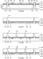
- a device 100 with a matrix of photo-emitting and/or photo-receiving diodes 102, according to a first exemplary embodiment, is described below in connection with the figures 1 and 2 .
- the figure 1 represents a sectional view of the device 100 along an axis AA visible on the figure 2
- the picture 2 represents a top view of the device 100.
- the figures 1 and 2 correspond to partial views representing only part of the device 100.
- Device 100 comprises several diodes 102 arranged in a matrix. Each diode 102 can be considered as forming a pixel of the matrix of the device 100. Furthermore, in this first embodiment, the diodes 102 correspond to photo-emitting diodes, here LEDs or micro-LEDS.
- the device 100 comprises a support 104 on which the diodes 102 are arranged.
- the support 104 corresponds to an electronic control circuit, comprising for example CMOS electronic components, on which the diodes 102 are arranged and to which the diodes 102 are electrically connected.
- Such an electronic circuit can in particular be used to electrically control the diodes 102 when they correspond to photo-emitting diodes.
- this electronic circuit can be used to process the signals delivered by the diodes 102.
- the support 104 can correspond to a passive element comprising no electronic components, such as for example an interconnection network, a card or an organic substrate.
- the diodes 102 are made in a stack of at least a first layer 106 of semiconductor arranged on a second layer 108 of semiconductor. Furthermore, in this first exemplary embodiment, the stack also comprises one or more emissive layers 110 arranged between the first and second layers 106, 108 and each intended to form, in the diodes 102, quantum wells.
- the first and second layers 106, 108 and the emissive layer(s) 110 may comprise one or more III-V type semiconductors, and advantageously GaN and/or InGaN. It is also possible that this or these semiconductor materials correspond to one or more of the following semiconductors: AlGaN, AlGaInN, InP, InGaP, AlGaP, AlGaInP, GaAs, InGaAs, AlGaAs.
- the semiconductors in layers 106 and 108 are doped with different conductivity types.
- the semiconductor of the first layer 106 is n-doped and that of the second layer 108 is p-doped.
- the semiconductor of the first layer 106 it is possible for the semiconductor of the first layer 106 to be p-doped and for that of the second layer 108 to be n-doped.
- the first layer 106 may correspond to a superposition of several distinct semiconductor layers, for example an n+ doped semiconductor layer with a concentration of donors for example comprised between approximately 5.10 17 and 5.10 20 donors/ cm 3 on which is arranged another layer of n- doped semiconductor (with a concentration of donors lower than that of the layer of n+ doped semiconductor) for example between about 10 17 and 5 ⁇ 10 19 donors/cm 3 .
- the n+ doped semiconductor layer may comprise GaN and the n ⁇ doped semiconductor layer may comprise InGaN.
- the thickness of the n+ doped semiconductor layer is for example greater than about 100 nm, and for example equal to about 3 ⁇ m, and that of the n- doped semiconductor layer is for example between about 5 nm and 500nm.
- the layer of n+ doped semiconductor can form a buffer layer arranged between the layer of n- doped semiconductor and a substrate (not visible on the figures 1 and 2 , and which corresponds to the substrate from which the stack of layers is made) serving in particular to filter the growth defects of the n- doped semiconductor layer so that these defects are not found in this n+ doped layer.
- the total thickness of the first layer 106 is for example between approximately 20 nm and 10 ⁇ m, and preferably between approximately 2 ⁇ m and 4 ⁇ m.
- the first layer 106 may correspond to a single layer of n-doped semiconductor, and with a concentration of donors for example between approximately 10 17 and 5.10 20 donors/cm 3 , comprising for example GaN and whose the thickness is for example between about 20 nm and 10 ⁇ m, and advantageously between about 2 ⁇ m and 4 ⁇ m.
- the emissive layer or layers 110 comprise so-called intrinsic semiconductor materials, that is to say not intentionally doped (with a concentration of residual donors n nest for example equal to around 10 17 donors/cm 3 , or between around 10 15 and 10 18 donors/cm 3 ).
- the emissive layer or layers 110 comprise for example InGaN.
- the emissive layer 110 or each of the emissive layers 110 is arranged between two barrier layers (not visible in the figures), comprising for example GaN.
- the emissive layer or layers 110 are arranged on the first layer 106.
- the thickness of the or each of the emissive layers 110 is for example equal to around 3 nm and more generally between around 0.5 nm and 10 nm, and the thickness of each of the barrier layers is for example between approximately 1 nm and 25 nm.
- the second layer 108 is placed on the emissive layer or layers 110, or directly on the first layer 106 when the stack does not include an emissive layer 110.
- the semiconductor of the second layer 108 is for example GaN and its thickness is for example between approximately 20 nm and 10 ⁇ m.
- the second layer 108 has for example a concentration of acceptors of between about 10 17 and 5 ⁇ 10 19 acceptors/cm 3 .
- an electron blocking layer (not visible on the figures 5 to 9 ) can be placed between the second layer 108 and the emissive layer or layers 110, this electron blocking layer comprising for example AlGaN with for example approximately 12% aluminum and p-doped with a concentration of acceptors by example equal to approximately 1.10 17 acceptors/cm 3 .
- the device 100 also comprises first trenches 112 which, in this first embodiment, pass through the entire thickness of the stack of layers 106, 108, 110. These first trenches 112 are for example produced by forming a grid. These first trenches 112 delimit several regions of the stack (and more generally at least one region of the stack) forming the pn junctions of the diodes 102. The distance between two first trenches 112 adjacent and parallel to each other is for example equal to approximately 90 ⁇ m. In the embodiment described here, the diodes 102 will be made in the form of mesa structures, or island structures, delimited by the first trenches 112.
- the regions of the stack surrounded by the first trenches 112 have for example a section , in a plane parallel to the face of the support 104 on which the stack is located, for example in the shape of a disc or a rectangle or more generally a polygon (square shape on the example of the figures 1 and 2 ).
- the first trenches 112 are regularly spaced from each other and delimit regions of the stack of substantially similar dimensions from each other.
- Dielectric portions 114 are arranged in each of the first trenches 112 and cover the lateral flanks of the regions of the stack surrounded by the first trenches 112. The dielectric portions 114 cover these lateral flanks over the entire thickness of the second layer 108 and of the layer(s) 110, as well as over a first part of the thickness of the first layer 106. On the figure 1 , this first part of the thickness of the first layer 106 is called e 1 . Depending on the total thickness of the first layer 106, the first part of the thickness of the first layer 106 e 1 is for example between approximately 100 nm and 5 ⁇ m.
- the dielectric portions 114 comprise for example SiO 2 and/or SiN.
- First electrically conductive portions 116 are arranged in each of the first trenches 112. These first portions 116 cover the side flanks of the regions of the stack surrounded by the first trenches 112. The first portions 116 cover these side flanks over a second part of the stack. thickness of the first layer 106. On the figure 1 , this second part of the thickness of the first layer 106 is called e 2 . Thus, the first portions 116 are electrically connected to the n-doped semiconductor material of the first layer 106. In addition, thanks to the presence of the dielectric portions 114 in each of the first trenches 112, the first electrically conductive portions 116 are electrically insulated from the second layer 108 and the layer or layers 110. In order to optimize the quality of the electrical contact between the first electrically conductive portions 116 and the first layer 106, it will be sought to maximize the ratio e2/e1.
- the device 100 also comprises second trenches 118 (and more generally at least one second trench 118) partially crossing the thickness of the first layer 106 from a face 120 of the first layer 106 opposite to that located opposite, or on the side , of the second layer 108.
- This face 120 corresponds to the emissive face of the diodes 102.
- These second trenches 118 separate, within one or more regions of the stack surrounded by the first trenches 112, several portions of the first layer 106 in order to optically separate, within the or each of these regions of the stack, several diodes 102.
- the thickness of the first layer 106 which is not crossed by the second trenches 118 is for example between 20 nm and 500 nm, or between 100 nm and 500 nm. It is possible that the thickness of the first layer 106 which is not crossed by the second trenches 118 is equal to e 1 .
- each of the first and second trenches 112, 118 is for example between approximately 0.5 ⁇ m and 5 ⁇ m.
- the widths of the first trenches 112 can be similar or different from those of the second trenches 118.
- the second trenches 118 can be filled at least partially with one or more optically reflective materials, for example one or more metallic materials, forming second electrically conductive portions.
- the second electrically conductive portions make it possible to improve the optical isolation between the pixels produced in the same region of the stack surrounded by first trenches 112.
- the material of the first electrically conductive portions 116, and possibly that of the second electrically conductive portions when such second portions are present in the second trenches 118, correspond for example to one of the following materials: Al, Ag, Au, Cu.
- the first electrically conductive portions 116 form first electrodes of the diodes 102 electrically connected to the n-doped semiconductor of the diodes 102.
- the first electrodes of all the diodes 102 of the matrix of the device 100 are formed by the first portions 116 and are electrically connected to each other, for example at an edge of the matrix, and form a first electrode (here a cathode) common to all these diodes 102.
- the first electrodes are electrically connected to the control circuit forming the support 104.
- the first electrodes of the diodes 102 produced in the regions of the stack through which the second trenches 118 pass are formed by the first electrically conductive portions 116 and by the second electrically conductive portions .
- the character electrically conductive of the second electrically conductive portions makes it possible to ensure electrical contact with the first electrodes.
- each of the diodes 102.1 and 102.2 is formed by a region of the stack surrounded by first trenches 112 and these regions are not crossed by second trenches 118.
- the four diodes 102.3, 102.4, 102.5 and 102.6 are formed in a single region of the stack surrounded by first trenches 112 and which is crossed by second trenches 118 separating the part of the first layer 106 of this region of the stack into four portions, each of these four portions forming part of one of the four diodes 102.3, 102.4, 102.5 and 102.6. It is the same for the four diodes 102.7, 102.8, 102.9 and 102.10.
- Each of the diodes 102 also comprises a second electrode electrically coupled to the portion of the second layer 108 forming the p-n junction of this diode 102.
- each second electrode is formed by an electrically conductive portion 122 placed against the portion of the second layer 108 and by an electrical connection element 124 connecting the electrically conductive portion 122 to the electronic control circuit forming the support 104.
- the electrically conductive material of the portions 122 is for example optically reflective, and corresponds for example to aluminum or silver.
- the electrically conductive portions 122 of the second electrodes of these diodes are electrically insulated from each other.
- the pattern etched in the electrically conductive layer (from which the portions 122 are made) to isolate these portions 122 from each other can be similar to that of the second trench or trenches 118 crossing the region of the stack.
- Each of the second electrodes 122 is electrically connected to the control circuit forming the support 104 individually in order to be able to drive each of the diodes 102 individually.
- a dielectric material 126 is present around the electrical connection elements 124 to ensure their electrical insulation from each other as well as their mechanical protection vis-à-vis the environment.
- the density of diodes 102 within this matrix is not uniform. In this first example, this density is quadrupled at the center of the matrix, at the level of four regions of the stack each surrounded by first trenches 112.
- the pixelization pitch of the matrix of diodes 102 that is to say the distance between the centers of two neighboring diodes 102, obtained in the regions which comprise the second trenches 118 is for example equal to 45 ⁇ m, while this pixelization pitch in the regions which do not comprise the second trenches is for example equal to 90 ⁇ m. More generally, the pixelization pitch of the diodes 102 defined by the first trenches 112 is typically between approximately 1 ⁇ m and 500 ⁇ m.
- the picture 3 represents, schematically and seen from above, another embodiment of the device 100 in which four regions of the stack of layers are each divided into nine sub-regions each forming a diode 102. Each of these regions of the stack is surrounded by first trenches 112. It should be noted that in this configuration, in each of the four central regions, the sub-region located in the center does not comprise a lateral flank formed by one of the first trenches 112. Thus, when the second trenches 118 are not filled with an electrically conductive material, this central sub-region does not form a diode since the semiconductor portion of the first layer 106 of this sub-region is not electrically connected to a first electrode formed in the first trenches 112.
- the second electrically conductive portions are in electrical contact with the first electrically conductive portions 116 of the first electrodes. All the lateral flanks of the different sub-regions are therefore in electrical contact with an element (first electrically conductive portions 116 or second portions electrically conductive) forming a first electrode for each of the diodes 102 of these sub-regions.
- the figure 4 shows another embodiment of the device 100 in which three regions of the stack of layers are each divided into eight sub-regions each forming a diode 102. Each of these regions of the stack is surrounded by first trenches 112. In this configuration, all the pn junctions formed in each of these three regions comprise at least one side flank in electrical contact with one of the first trenches 112. All the parts of each of these regions form functional diodes 102, whether the second trenches 118 are filled or not with an electrically conductive material.
- the number of distinct diodes separated by the second trenches 118 within a region of the stack surrounded by first trenches 112 is greater than or equal to 2 and can reach several thousand or even several million or more depending on the final resolution of the device.
- the density of diodes 102 is greater at the center of the matrix of diodes 102 than at the edges of the matrix. As a variant, it is possible for this higher density of diodes to be located at one or more places in the matrix other than the center.
- a method of making the device 100 according to a first embodiment is described below in connection with the figures 5 to 9 .
- the device 100 comprises a matrix of diodes 102 forming a matrix of pixels of the device 100.
- the diodes 102 correspond to photo-emitting diodes, here LEDs.
- the device 100 is made from a substrate 128 comprising for example sapphire and/or silicon and/or a semiconductor for example similar to that used to form the active part of the diodes 102, and/or silicide carbon and/or glass and/or any other material allowing the substrate 128 to form a growth substrate allowing the production of the semiconductor stack forming the active part of the diodes 102 by epitaxy.
- the substrate 128 serves as a support for the deposition and/or growth of layers intended for the production of diodes 102 of device 100.
- the stack of layers from which the diodes 102 are going to be made is formed on the substrate 128.
- This stack comprises the first semiconductor layer 106, the emissive layer(s) 110, the second semiconductor layer 108 and a electrically conductive layer 130 forming, in each of the diodes 102, the portions 122 of the second electrodes (corresponding to the anode in the example described here) which will be in contact with the semiconductor of the second layer 108.
- the electrically conductive layer 130 is placed on the second layer 108.
- a first step forming the electrically conductive layer 130 is implemented in order to produce the portions 122 of the second electrodes of the diodes 102.
- This layer 130 is for example deposited on the layer 108 then removed locally by a so-called “lift-off” process in order to to form the portions 122 which will be, within the same region of the stack, surrounded by first trenches 112 and comprising one or more second trenches 118, electrically insulated from each other.
- the structure obtained at this stage of the process is represented on the figure 5 .
- the areas removed from the electrically conductive layer 130 are arranged substantially opposite the regions where the second trenches 118 will be made subsequently.
- a layer intended to form a dielectric hard mask is then placed on the electrically conductive layer 130.
- the material of this layer is for example SiO 2 or SIN.
- This layer is etched to form a hard dielectric mask 132 which will serve in particular as a mask for etching the other layers of the stack.
- the pattern of this hard mask 132 corresponds to that of the first trenches 112.
- etching through the layers 130, 108, 110 and a first part of the thickness of the first layer 106 is then implemented according to the pattern of the hard dielectric mask 132.
- This etching corresponds for example to a dry etching, for example by a Cl 2 -based plasma or an RIE etching, for example ICP-RIE (reactive ion etching by a plasma torch system, or “Inductively Coupled Plasma—Reactive Ion Etching”).
- This etching is stopped at a depth level located in the first layer 106 and such that the bottom walls of the etched trenches are formed by the first layer 106.
- the thickness of the first layer 106 etched during this etching is equal to l thickness e 1 .
- This etching is carried out such that the remaining thickness of the first layer 106, that is to say the second part of the thickness of the first layer 106 e 2 , is sufficient to make good electrical contact between the semiconductors of the first layer 106 and the first electrically conductive portions 116 which will be made later in the first trenches 112. This etching forms a first part of the first trenches 112.
- a dielectric layer corresponding for example to a SiN/Si0 2 bilayer or comprising Al 2 O 3 , and forming a passivation layer, is then deposited with a conforming thickness, for example comprised between around 5 nm and 1 ⁇ m and advantageously equal to approximately 200 nm, on the hard mask 132 and along the walls of the first parts of the first trenches 112, therefore covering the side walls formed of the hard mask 132 and of the regions of the stack of layers 106, 108, 110, 130 which are surrounded by the first parts of the first trenches 112 engraved.
- the dielectric layer is also deposited on the non-etched parts of the first layer 106 forming the bottom walls of these first parts of the first trenches 112.
- This dielectric layer is for example formed by a deposit of the PECVD type (chemical vapor deposition assisted by plasma) or ALD (atomic layer deposition) depending on the nature of the material(s) deposited.
- Anisotropic etching for example dry etching such as RIE etching, is then implemented such that the parts of the dielectric layer located in the first parts of the first trenches 112 and not covering the side walls of the first parts of the first trenches 112 are removed, thus revealing the parts of the first layer 106 lying at the bottom of the first parts of the first trenches 112.
- the parts of this dielectric layer covering the upper face of the hard mask 132 are also removed. Thus, only the portions 114 of the dielectric layer covering the side walls of the first parts of the first trenches 112 are retained.
- a second etching of the stack is implemented, extending the first trenches 112 through the remaining thickness e 2 of the first layer 106 of semiconductor until reaching the substrate 128, that is to say until 'so that the bottom walls of the first trenches 112 are formed by the substrate 128. form electrical contact areas for the first electrically conductive portions 116.
- Openings are then made through dielectric mask 132, forming locations for making electrical connection elements 124 intended to ensure electrical contacts with the second electrodes. These openings pass through the entire thickness of the dielectric mask 132 so that the bottom walls of these openings are formed by the electrically conductive portions 122. This etching is for example of the ICP-RIE type.
- One or more electrically conductive materials are then deposited in the first trenches 112 and in the locations of the electrical connections 124, forming the first electrically conductive portions 116 and the electrical connection elements 124.
- a first electrically conductive material can be deposited in the first trenches 112 and in the locations of the electrical connection elements 124 as well as on the dielectric mask 132.
- This first electrically conductive material is deposited conformally, it that is to say, by forming a layer of substantially constant thickness on the dielectric mask 132 and along the side walls and the bottom walls of the first trenches 112 and of the locations of the electrical connection elements 124.
- this first material electrically conductive can be formed by the deposition, for example of the PVD type, of a first layer of titanium with a thickness for example of less than approximately 300 nm, followed by a deposition, for example PVD, of a second layer of aluminum with a thickness for example between about 50 nm and 1 ⁇ m.
- the deposition techniques implemented are chosen so that they are adapted to the significant form factor of the volumes formed by the first trenches 112, and correspond for example to those implemented to deposit the electrically conductive material(s) of the conductive vias or TSV (“Through-Silicon Via”).
- a second electrically conductive material can be deposited by filling the remaining volumes of the first trenches 112 and of the locations of the electrical connection elements 124.
- the thickness of this second electrically conductive material can be such that it also covers the parts of the first electrically conductive material arranged on the dielectric mask 132.
- This second electrically conductive material is for example copper which can be formed by the implementation of a full plate electrochemical deposition (ECD or "Electro-Chemical Deposition"), it is that is to say on the whole of the structure previously carried out.
- a chemical-mechanical planarization (CMP) can then be implemented in order to remove the portions of the first and second electrically conductive materials which protrude from the first trenches 112 and from the locations of the electrical connection elements 124. This planarization makes it possible to complete the production electrically conductive portions 116 and electrical connections 124 and to electrically insulate these electrically conductive portions 116 vis-à-vis the electrical connections 124.
- the structure obtained at this stage of the process corresponds to that visible on the figure 6 .
- device 100 includes other regions of the stack also surrounded by first trenches 112 and which are not visible in these figures.
- the first electrically conductive portions 116 are electrically well insulated from the layers 108 and 110.
- the thickness of the dielectric portions 114 can be chosen such that an acceptable leakage current is tolerated on each of the diodes 102, by example less than approximately 1% of the nominal current passing through diode 102, when they are subjected to a potential difference (applied between the cathode and the anode) for example of the order of 4 volts.
- the minimum thickness of the dielectric portions 114 is for example comprised between approximately 3 nm and 5 nm, or between 3 nm and 4 nm, depending on the material or materials used to produce the dielectric portions 114.
- the structure produced is then hybridized on the support 104.
- this hybridization can correspond to a direct bonding (“direct bonding”, also called bonding by molecular adhesion), or a copper-oxide hybrid bonding and Au/Au thermocompression, or make use of electrical connection elements between the matrix of diodes 102 (and more specifically the electrical connection elements 124) and the electronic circuit such as, for example, fusible alloy balls (comprising for example SnAg and/or indium ), or to copper pillars covered with solder material, or to micro-inserts, or to micro-tubes.
- direct bonding also called bonding by molecular adhesion
- copper-oxide hybrid bonding and Au/Au thermocompression or make use of electrical connection elements between the matrix of diodes 102 (and more specifically the electrical connection elements 124) and the electronic circuit such as, for example, fusible alloy balls (comprising for example SnAg and/or indium ), or to copper pillars covered with solder material,
- the substrate 128 is removed, thus freeing the rear faces of the diodes through which the light is intended to enter or leave depending on whether the diodes 102 are photo-emitting or photo-receiving diodes (see figure 7 ).
- the substrate 128 is for example removed by laser lifting ("laser lift-off" in English) when the substrate 128 comprises sapphire, or by grinding (“grinding" in English) and selective chemical attack when the substrate 128 comprises for example a semiconductor such as silicon.
- the second trenches 118 are then made through part of the thickness of the first layer 106, such that the bottom walls of these second trenches 118 are formed by the material of the first layer 106 (see figure 8 ).
- the second trenches 118 are for example produced by implementing etching carried out using a hard mask, for example of SiO 2 . These second trenches 118 mark the physical and optical separation between the diodes 102 produced in the region of the stack surrounded by the first trenches 112.
- the second trenches 118 When the second trenches 118 are intended to be filled with at least one electrically conductive material performing a electrical contact with the semiconductor of the first layer 106, the second trenches 118 have at least an overlap region with the first trenches 112 to ensure continuity of electrical contact with the semiconductor of the first layer 106.
- the production of the device 100 is completed by the filling of the second trenches 118 with at least one electrically conductive material forming second electrically conductive portions 134 (see figure 9 ).
- This filling can be obtained by implementing steps similar to those implemented to produce the first electrically conductive portions 116.
- the hard mask used during the etching and filling of the second trenches 118 can be kept if it is transparent to the radiation, or suppressed, or even structured (for example by photonic crystals) to improve the light extraction or the directivity of emission.
- a transparent electrically conductive material for example ITO (indium and tin oxide) or AZO (zinc and aluminum oxide) or GZO ( zinc and gallium oxide), on the upper face of the assembly produced in order to improve the electrical contact between the semiconductor of the first layer 106 and the first and second electrically conductive portions 116, 134.
- a transparent electrically conductive material for example ITO (indium and tin oxide) or AZO (zinc and aluminum oxide) or GZO ( zinc and gallium oxide)
- the transfer of the diodes 102 onto the support 104 corresponds to a substrate-to-substrate, or “wafer-to-wafer” connection, that is to say that several matrices of diodes 102 are produced simultaneously in the layers 106, 108, 110 and that these matrices are transferred together on a substrate forming the support 104.
- This configuration is schematized on the figure 10 , on which the reference 136 designates the connection interface (bonding, interconnection elements, etc.) between the diode matrices 102 and the substrate forming the support 104.
- the matrices of diodes 102 produced simultaneously in the layers 106, 108, 110 to be first of all cut out in the form of individual chips, then transferred individually onto the substrate forming the support 104.
- This variant corresponds to an attachment of chip-to-substrate type, or "chip-to-wafer", implemented with the hybridization techniques mentioned above.
- the spaces between the diode arrays 102 are filled with a material 138, for example a dielectric. This configuration is schematized on the figure 11 .
- the matrices of diodes 102 produced simultaneously in the layers 106, 108, 110 can be first of all cut out in the form of individual chips, then transferred individually onto the substrate forming the support 104 also previously cut out in the form of individual chips.
- This other variant corresponds to chip-to-chip or "chip-to-chip” type connection.
- Each assembly formed by a matrix of diodes 102 and a control circuit is then transferred to another support 140 and the spaces between the sets "chips of diode matrices 102 transferred to chips of support substrates 104" are filled with a material 138, for example a dielectric.
- This configuration is schematized on the figure 12 .
- a cutting step is implemented to separate the devices 100 from each other.
- the first trenches 112 are made by etching the entire thickness of the stack formed by the layers 106, 108 and 110.
- the second etching of the stacking implemented after having produced the dielectric portions 114 is not carried out through the entire remaining thickness of the first layer 106, but through only part of this remaining thickness.
- the first electrically conductive portions 116 produced in the first trenches 112 are in electrical contact with the material of the first layer 106 at the level of the parts of the side walls of the first trenches 112 which are not covered by the dielectric portions 114 and at the level of the bottom walls of the first trenches 112.
- the first layer 106 is formed from the face against which the substrate 128 was previously located, until reaching the first electrically conductive portions 116.
- This thinning makes it possible to reduce the optical crosstalk between the pixels and makes it possible to reduce the width of the first trenches 112 while maintaining a constant aspect ratio (lithography and deep etching constraint).
- the first trenches 112 are etched, before transfer onto the support 104, through the layers 130, 106, 108 and 110 with a depth equal to the desired height for the first electrically conductive portions 116.
- the first trenches 112 are etched, before the transfer onto the support 104, partially through the entire thickness of the layer 130, of the second layer 108 (and of the emissive layer(s) 110 if such layers are present in the stack) and through only part (thickness e 1 ) of the thickness of the first layer 106.
- the dielectric portions 114 and electrically conductive portions 136, forming first parts of the portions 116, are then made in those parts of the first trenches 112 which do not cross the entire thickness of the first layer 106 (see figure 13 ).
- the assembly is then transferred to the support 104, as in the first embodiment.
- An etching is then implemented to finish etching the first trenches 112 and at the same time etch the second trenches 118 (see figure 14 ).
- the first trenches 112 and the second trenches 118 are then filled with one or more electrically conductive materials, thus completing the production of the first electrically conductive portions 116 and forming the second electrically conductive portions 134 (see figure 15 ).
- the first electrically conductive portions 116 are therefore produced in two stages. This is advantageous because the remaining thickness (thickness e 2 ) of the first layer 106 which is not etched during the production of the first part of the portions 116 (step visible on the figure 13 ) corresponds to the depth of the second trenches 118. The first parts 136 of the portions 116 then form an etching stop material during the making of the second trenches 118 and the completion of the first trenches 112.
- this second production method it is also possible to thin the first layer 106 after the removal of the substrate 128 and before the etching of the second trenches 118. doped arranged on the side of the substrate 128, this thinning being able to eliminate this undoped part.
- This second embodiment also makes it possible to relax the constraints on the width of the first trenches 112. Indeed, given that the etching of these trenches requires the implementation of two distinct steps, on both sides of the stack, the depth of material to be etched at each of these two steps is therefore less than when the first trenches 112 are made with the implementation of a single etching step, which makes it possible to reduce the aspect ratio in English, i.e. the ratio of the value of the depth of a trench to the value of the width of the trench) of the trenches. This thinning therefore ultimately makes it possible to obtain first trenches 112 that are narrower than when they are made with the implementation of a single etching step through the entire thickness of the layers 130, 106, 108 and 110.
- the matrix of pixels produced comprises several regions of the stack each surrounded by first trenches, and second trenches are produced in at least part of these regions.
- the matrix of pixels of device 100 it is possible for the matrix of pixels of device 100 to comprise a single region of the stack surrounded by first trenches 112, and for this region to be crossed by second trenches 118 which therefore define the pitch of all the pixels of this matrix.
- the figure 16 corresponds to a top view of such an embodiment.
- This other exemplary embodiment is very advantageous because in all the pixels of the matrix, there is no damage to the lateral flanks of the portions of the layers 108 and 110.
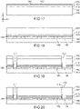
- a method of making the device 100 according to a third embodiment is described below in connection with the figures 17 to 22 .
- a stack similar to that previously described in connection with the figure 5 is made on the substrate 128.
- the etched spaces between the electrically conductive portions 122 are filled with a dielectric material 142 deposited and planarized with a stop on the portions 122 (see figure 17 ).
- first electrical contacts 144 are made on the support 104 and are intended to be connected to the electrically conductive portions 122.
- Second electrical contacts 146 are also made on the support 104 and are intended to be connected to the first electrically conductive portions 116.
- the first and second electrical contacts 144, 146 are connected to the electronic control circuit of the support 104 and are electrically insulated from each other by a dielectric material 148 deposited between these contacts (see figure 18 ).
- the substrate 128 is removed.
- the hard mask 132 is then produced on the stack, then the first trenches 112 are etched through the entire thickness of the layers 106, 108, 110, until reaching the first electrical contacts 146.
- the dielectric portions 114 are then made in the first trenches 112, against the side flanks of the layers 108, 110 and on the first part of the thickness e 1 of the first layer 106 (see figure 19 ).
- the dielectric portions 114 are for example made as described in the document FR 3 073 669 A1 .
- the first electrically conductive portions 116 are then made in the remaining volume of the first trenches 112, by implementing steps similar to those previously described for the first and second embodiments (see figure 20 ).
- the pattern of the second trenches 118 is then etched into the hard mask 132, then through part of the thickness of the first layer 106 ( figure 21 ).
- the device 100 is then completed by filling the second trenches 118 with at least one electrically conductive material forming the second electrically conductive portions 134 (see figure 22 ).
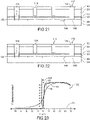
- the figure 23 represents simulations of illumination carried out in a pixel of GaN defined by second trenches similar to those carried out within the device 100. This simulation is obtained with a pixel formed in a stack of GaN of height equal to 7 ⁇ m, with these trenches which do not cross a part of the GaN with a thickness equal to 200 nm. The light emission occurs in the part of the thickness not crossed by the second trenches 118, which bears the reference 20 on the figure 23 .
- the width of the second trench 118 visible on the figure 23 is equal to 3 ⁇ m.
- curve 10 represents the relative illumination obtained in the absence of the second trench 118
- curve 12 represents the relative illumination obtained in the presence of the second trench 118 when the latter is not filled by a electrically conductive material and here filled with air
- the curve 14 represents the relative illumination obtained in the presence of the second trench 118 when the latter is filled with aluminum forming a second electrically conductive portion 134.
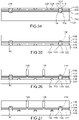
- a method of making the device 100 according to a fourth embodiment is described below in connection with the figures 24 to 27 .
- the first trenches 112 are etched, before the transfer onto the support 104, partially through the entire thickness of the layer 130, of the second layer 108 (and of the emissive layer(s) 110 if such layers are present in the stack) and through only part (thickness e 1 ) of the thickness of the first layer 106.
- the dielectric portions 114 and the first electrically conductive portions 116 are then made in the first trenches 112 which do not do not cross the entire thickness of the first layer 106 (see figure 24 ). At this stage of the process, the first electrically conductive portions 116 are completed and are in electrical contact with the material of the first layer 106 at the level of the bottom walls 150 of the first trenches 112.
- the assembly is then transferred to the support 104, as in the second embodiment (see figure 25 ).
- the second trenches 118 are then filled with one or more electrically conductive materials, forming the second electrically conductive portions 134 (see figure 27 ).
- the device 100 comprises a matrix of diodes 102 which are light-emitting diodes, the microelectronic device being able to form part of an LED display device (screens, projector, wall of pictures, etc.).
- This matrix of diodes 102 comprises the first electrically conductive portions 116 which form a cathode common to all the diodes 102, and each diode 102 comprises a second electrically conductive portion 122 forming an anode allowing individual addressing of each of the diodes 102.
- the microelectronic device 100 can comprise a matrix of diodes 102 which are photo-receiving diodes, or photodiodes.
- the anodes and the cathodes of the diodes 102 are not used to supply current to the diodes 102 but to recover the currents photo-generated by the diodes 102.
- the diodes 102 may not include layers 110 of intrinsic semiconductor between the first and second layers 106, 108. In this case, the p and n doped semiconductors are then placed directly against each other.
- optical elements on the diodes 102, for example phosphors modifying the wavelength emitted by the diodes 102.
Description
L'invention concerne le domaine des dispositifs à diodes photo-émettrices, telles que des diodes électroluminescentes (appelées DELs ou LEDs, ou encore micro-LEDs), et/ou à diodes photo-réceptrices telles que des photodiodes. L'invention s'applique notamment aux domaines suivants :
- dispositifs d'éclairage par LEDs, dispositifs électroniques comprenant des matrices de LEDs tels que des écrans, des projecteurs, des murs d'images, ou des dispositifs d'éclairage comme par exemple des phares pour véhicule ;
- dispositifs électroniques ou microélectroniques photorécepteurs comportant des matrices de photodiodes, tels que des capteurs d'images ;
- dispositifs comportant à la fois des diodes photo-émettrices et des diodes photo-réceptrices, formant par exemple à la fois un capteur et un écran.
- LED lighting devices, electronic devices comprising matrices of LEDs such as screens, projectors, video walls, or lighting devices such as, for example, vehicle headlights;
- electronic or microelectronic photoreceptor devices comprising arrays of photodiodes, such as image sensors;
- devices comprising both photo-emitting diodes and photo-receiving diodes, forming for example both a sensor and a screen.
Dans un dispositif à diodes photo-émettrices et/ou photo-réceptrices, il est souvent avantageux d'augmenter la résolution du dispositif, c'est-à-dire d'augmenter le nombre de cellules actives, ou pixels, par unité de surface du dispositif. Cette augmentation de la résolution implique de diminuer la taille unitaire des pixels tout en essayant de ne pas augmenter la diaphonie (ou en « cross-talk » en anglais), c'est-à-dire les interférences optiques se produisant entre pixels adjacents et de minimiser la diminution de performances des diodes généralement observée sur les petits pixels.In a device with photo-emitting and/or photo-receiving diodes, it is often advantageous to increase the resolution of the device, that is to say to increase the number of active cells, or pixels, per unit area. of the device. This increase in resolution involves reducing the unit size of the pixels while trying not to increase crosstalk (or "cross-talk"), that is to say the optical interference occurring between adjacent pixels and to minimize the decrease in performance of diodes generally observed on small pixels.
Le document
Cette gravure définissant les pixels provoque des défauts dans le matériau semi-conducteur car elle endommage tous les flancs latéraux des structures mesa, provoquant ainsi une diminution des performances, notamment l'efficacité quantique externe (EQE), des diodes photo-émettrices et/ou photo-réceptrices lorsque leur taille diminue.This etching defining the pixels causes defects in the semiconductor material because it damages all the side flanks of the mesa structures, thus causing a decrease in performance, in particular the external quantum efficiency (EQE), of the photo-emitting diodes and/or photoreceptors when their size decreases.
De plus, le procédé proposé dans le document
Le document
Les procédés technologiques de fabrication mis en jeu ne sont en outre que peu compatibles avec des variations de densité de motifs au sein de la matrice.Furthermore, the technological manufacturing processes involved are only slightly compatible with variations in the density of patterns within the matrix.
Un but de la présente invention est de proposer un dispositif à matrice de diodes photo-émettrices et/ou photo-réceptrices dont la structure permet une réalisation en limitant l'endommagement des flancs latéraux des diodes, et qui soit compatible avec une densité de diodes variable au sein de la matrice.An object of the present invention is to provide a device with a matrix of photo-emitting and/or photo-receiving diodes, the structure of which allows production by limiting the damage to the side flanks of the diodes, and which is compatible with a density of diodes variable within the matrix.
Pour cela, l'invention propose un dispositif à matrice de diodes photo-émettrices et/ou photo-réceptrices, formant une matrice de pixels du dispositif, comportant au moins :
- un empilement d'au moins une première et une deuxième couches de semi-conducteurs dopés selon des types de conductivité différents, chacune des diodes comportant une portion de la première couche superposée à une portion de la deuxième couche ;
- des premières tranchées traversant toute l'épaisseur de la deuxième couche et au moins une partie de l'épaisseur de la première couche et entourant au moins une région de l'empilement dans laquelle sont formées plusieurs diodes ;
- des portions diélectriques disposées dans les premières tranchées et recouvrant des flancs latéraux de ladite région de l'empilement sur toute l'épaisseur de la deuxième couche et une première partie de l'épaisseur de la première couche ;
- des premières portions électriquement conductrices disposées dans les premières tranchées, recouvrant les flancs latéraux de ladite région de l'empilement sur une deuxième partie de l'épaisseur de la première couche non recouverte par les portions diélectriques et/ou recouvrant des parois de fond des premières tranchées, et formant au moins une partie de premières électrodes des diodes formées dans ladite région de l'empilement ;
- au moins une deuxième tranchée traversant partiellement l'épaisseur de la première couche depuis une face opposée à celle se trouvant en regard de la deuxième couche, c'est-à-dire depuis une première face de la première couche opposée à une deuxième face de la première couche se trouvant en regard de la deuxième couche, et séparant les portions de la première couche des diodes formées dans ladite région de l'empilement sans traverser l'interface entre les première et deuxième couches ;
- plusieurs deuxièmes électrodes isolées électriquement les unes des autres et chacune reliée électriquement à l'une des portions de la deuxième couche des diodes formées dans ladite région de l'empilement.
- a stack of at least a first and a second layer of semiconductors doped according to different types of conductivity, each of the diodes comprising a portion of the first layer superimposed on a portion of the second layer;
- first trenches crossing the entire thickness of the second layer and at least part of the thickness of the first layer and surrounding at least one region of the stack in which several diodes are formed;
- dielectric portions arranged in the first trenches and covering the side flanks of said region of the stack over the entire thickness of the second layer and a first part of the thickness of the first layer;
- first electrically conductive portions arranged in the first trenches, covering the side flanks of said region of the stack over a second part of the thickness of the first layer not covered by the dielectric portions and/or covering the bottom walls of the first trenches, and forming at least a part of first electrodes of the diodes formed in said region of the stack;
- at least one second trench partially crossing the thickness of the first layer from a face opposite that facing the second layer, that is to say from a first face of the first layer opposite a second face of the first layer being opposite the second layer, and separating the portions of the first layer from the diodes formed in said region of the stack without crossing the interface between the first and second layers;
- several second electrodes electrically insulated from each other and each electrically connected to one of the portions of the second layer of diodes formed in said region of the stack.
Les portions de la deuxième couche des diodes formées dans ladite région de l'empilement forment une portion de semi-conducteur continue qui n'est pas traversée par les premières et deuxième tranchées.The portions of the second layer of diodes formed in said region of the stack form a continuous semiconductor portion which is not crossed by the first and second trenches.
Dans un tel dispositif, les flancs latéraux des diodes définis par la ou les deuxièmes tranchées ne sont pas endommagés au niveau de l'interface entre les première et deuxième couches puisque la ou les deuxièmes tranchées ne traversent pas cette interface (les deuxièmes tranchées ne traversent qu'une partie de l'épaisseur de la première couche). La diminution des performances des diodes photo-émettrices et/ou photo-réceptrices engendrée par les premières tranchées est donc moindre, voire nulle, par rapport à celle observée lorsque tous les flancs latéraux de toutes les diodes de la matrice sont gravés sur toute l'épaisseur de l'empilement de couches à partir duquel les diodes sont réalisées.In such a device, the side flanks of the diodes defined by the second trench(es) are not damaged at the interface between the first and second layers since the second trench(es) do not cross this interface (the second trenches do not cross only part of the thickness of the first layer). The reduction in the performance of the photo-emitting and/or photo-receiving diodes generated by the first trenches is therefore less, or even zero, compared to that observed when all the side flanks of all the diodes of the matrix are etched over the entire thickness of the stack of layers from which the diodes are made.
Les deuxièmes tranchées ne traversent pas l'interface entre les première et deuxième couches afin de ne pas endommager les flancs latéraux des diodes définies par les deuxièmes tranchées. Autrement dit, les parties de cette interface se trouvant en regard, ou à l'aplomb, des deuxièmes tranchées ne sont pas traversées par ces deuxièmes tranchées ni par d'autres tranchées. De plus, les premières tranchées entourent au moins une région de l'empilement dans laquelle sont formées plusieurs diodes et ces diodes ne sont pas séparées les unes des autres par les premières tranchées.The second trenches do not cross the interface between the first and second layers so as not to damage the side flanks of the diodes defined by the second trenches. In other words, the parts of this interface located opposite, or plumb with, the second trenches are not crossed by these second trenches or by other trenches. Moreover, the first trenches surround at least one region of the stack in which several diodes are formed and these diodes are not separated from each other by the first trenches.
Ainsi, la structure proposée ici permet, grâce aux deuxièmes tranchées, de réduire ou même supprimer la dépendance de l'EQE des diodes de la matrice en fonction de la taille des diodes.Thus, the structure proposed here makes it possible, thanks to the second trenches, to reduce or even eliminate the dependence of the EQE of the diodes of the matrix as a function of the size of the diodes.
De plus, cette structure permet également de moduler aisément la résolution au sein de la matrice de pixels puisque la résolution initiale de la matrice définie par les premières tranchées peut être modifiée localement dans une ou plusieurs régions de la matrice en définissant des diodes de plus petites dimensions via la réalisation de la ou des deuxièmes tranchées.Moreover, this structure also makes it possible to easily modulate the resolution within the matrix of pixels since the initial resolution of the matrix defined by the first trenches can be modified locally in one or more regions of the matrix by defining diodes of smaller dimensions via the realization of the second trench or trenches.
Ici et dans tout le reste du document, le terme « diode » est utilisé pour désigner une diode photo-émettrice, comme par exemple une LED, ou une diode photo-réceptrice, comme par exemple une photodiode.Here and throughout the rest of the document, the term “diode” is used to designate a photo-emitting diode, such as for example an LED, or a photo-receiving diode, such as for example a photodiode.
Les semi-conducteurs des première et deuxième couches sont dopés selon des types de conductivité différents, c'est-à-dire que l'une des première et deuxième couches comporte un semi-conducteur dopé de type p et que l'autre des première et deuxième couches comporte un semi-conducteur dopé de type n.The semiconductors of the first and second layers are doped according to different types of conductivity, that is to say that one of the first and second layers comprises a p-type doped semiconductor and the other of the first and second layers comprises an n-type doped semiconductor.
Dans la définition ci-dessus du dispositif, la première partie de l'épaisseur de la première couche est disposée entre la deuxième couche et la deuxième partie de l'épaisseur de la première couche.In the above definition of the device, the first part of the thickness of the first layer is placed between the second layer and the second part of the thickness of the first layer.
Bien que la ou les deuxièmes tranchées ne traversent pas la deuxième couche et ne traverse pas l'interface entre les première et deuxième couches, cette ou ces deuxièmes tranchées assurent une isolation optique entre les diodes dont les portions de la première couche sont séparées par cette ou ces deuxièmes tranchées.Although the second trench or trenches do not cross the second layer and do not cross the interface between the first and second layers, this or these second trenches provide optical isolation between the diodes whose portions of the first layer are separated by this or these second trenches.
Le dispositif peut comporter en outre au moins une deuxième portion électriquement conductrice disposée dans la deuxième tranchée. La présence de cette deuxième portion électriquement conductrice dans la deuxième tranchée améliore l'isolation optique entre les pixels dont les portions de la première couche sont séparées par cette deuxième tranchée.The device may also comprise at least one second electrically conductive portion placed in the second trench. The presence of this second electrically conductive portion in the second trench improves the optical isolation between the pixels whose portions of the first layer are separated by this second trench.
De plus, la deuxième portion électriquement conductrice peut être couplée électriquement aux premières portions électriquement conductrices et former, avec les premières portions électriquement conductrices, les premières électrodes des diodes. Ce couplage électrique entre la ou les deuxièmes portions électriquement conductrices et les premières portions électriquement conductrices est par exemple obtenu en réalisant les premières et deuxièmes tranchées selon des motifs qui se croisent ou se superposent à certains endroits.Moreover, the second electrically conductive portion can be electrically coupled to the first electrically conductive portions and form, with the first electrically conductive portions, the first electrodes of the diodes. This electrical coupling between the second electrically conductive portion(s) and the first electrically conductive portions is for example obtained by making the first and second trenches according to patterns which intersect or overlap at certain places.
Le matériau de la ou des deuxièmes portions électriquement conductrices peut être avantageusement optiquement réflecteur. Ainsi, lorsque les diodes correspondent à des diodes photo-émissives, la présence de ce matériau optiquement réflecteur améliore l'extraction de la lumière émise par les diodes. Lorsque les diodes correspondent à des diodes photo-réceptrices, la présence de ce matériau optiquement réflecteur évite, au niveau d'un pixel, la dispersion du rayonnement reçu dans les pixels voisins. Que les diodes soient photo-émissives ou photo-réceptrices, la présence d'un tel matériau limite donc la diaphonie entre les diodes voisines.The material of the second electrically conductive portion(s) can advantageously be optically reflective. Thus, when the diodes correspond to photo-emissive diodes, the presence of this optically reflective material improves the extraction of the light emitted by the diodes. When the diodes correspond to photo-receiving diodes, the presence of this optically reflective material avoids, at the level of a pixel, the dispersion of the radiation received in the neighboring pixels. Whether the diodes are photo-emissive or photo-receptive, the presence of such a material therefore limits the crosstalk between neighboring diodes.
Les premières tranchées et les premières portions électriquement conductrices peuvent traverser toute l'épaisseur de l'empilement, ou toute l'épaisseur de la deuxième couche et une partie seulement de l'épaisseur de la première couche.The first trenches and the first electrically conductive portions can pass through the entire thickness of the stack, or the entire thickness of the second layer and only part of the thickness of the first layer.
Dans une configuration particulière :
- toutes les diodes de la matrice peuvent être formées dans ladite région de l'empilement, et
- chacune des diodes de la matrice peut être séparée d'une ou plusieurs diodes voisines par au moins une des deuxièmes tranchées.
- all diodes of the matrix can be formed in said region of the stack, and
- each of the diodes of the matrix can be separated from one or more neighboring diodes by at least one of the second trenches.
Cette configuration est très avantageuse car aucun flanc latéral des diodes de la matrice n'est endommagé (ceux se trouvant en périphérie de la matrice peuvent par exemple faire partie de pixels non fonctionnels ou non utilisés, appelés alors pixels mécaniques). Les performances des diodes de la matrice sont donc très bonnes, similaires ou identiques à des diodes de taille égale aux dimensions totales de la matrice. Selon une autre configuration :
- les premières tranchées peuvent entourer plusieurs régions de l'empilement dans lesquelles les diodes de la matrice sont formées, et
- une ou plusieurs de ces régions peuvent comporter chacune la deuxième tranchée ou plusieurs deuxièmes tranchées.
- the first trenches can surround several regions of the stack in which the diodes of the matrix are formed, and
- one or more of these regions may each comprise the second trench or several second trenches.
Cette autre configuration peut notamment être utilisée lorsque la matrice de diodes est réalisée avec différentes régions présentant des résolutions de pixels différentes. Dans cette configuration, les premières tranchées peuvent définir la résolution minimale au sein de la matrice, et la ou les deuxièmes tranchées peuvent être formées dans une ou plusieurs régions de la matrice où la résolution des pixels est plus importante.This other configuration can in particular be used when the matrix of diodes is produced with different regions having different pixel resolutions. In this configuration, the first trenches can define the minimum resolution within the matrix, and the second trench or trenches can be formed in one or more regions of the matrix where the resolution of the pixels is more important.
La ou les régions de l'empilement comportant la ou les deuxièmes tranchées (celles ayant une résolution plus importante) peuvent former une partie centrale de la matrice de diodes.The region or regions of the stack comprising the second trench or trenches (those having a higher resolution) can form a central part of the diode matrix.
Le dispositif peut comporter en outre un circuit électronique de contrôle sur lequel l'empilement des première et deuxième couches est disposé et auquel les premières et deuxièmes électrodes des diodes sont couplées électriquement.The device may further comprise an electronic control circuit on which the stack of the first and second layers is arranged and to which the first and second electrodes of the diodes are electrically coupled.
Le dispositif peut être tel que :
- les diodes correspondent à des photodiodes, l'empilement comportant en outre au moins une couche de semi-conducteur intrinsèque ou non intentionnellement dopé disposée entre les première et deuxième couches et telle que des flancs latéraux de la couche de semi-conducteur intrinsèque présents dans les premières tranchées soient recouverts par les portions diélectriques, les deuxièmes tranchées ne traversant pas la couche de semi-conducteur intrinsèque, ou
- les diodes correspondent à des LED, l'empilement comportant au moins une couche émissive à puits quantique disposée entre les première et deuxième couches et telle que des flancs latéraux de la couche émissive présents dans les premières tranchées soient recouverts par les portions diélectriques, les deuxièmes tranchées ne traversant pas la couche émissive.
- the diodes correspond to photodiodes, the stack further comprising at least one layer of intrinsic or unintentionally doped semiconductor disposed between the first and second layers and such as side flanks of the layer of intrinsic semiconductor present in the first trenches are covered by the dielectric portions, the second trenches not passing through the intrinsic semiconductor layer, or
- the diodes correspond to LEDs, the stack comprising at least one quantum well emissive layer arranged between the first and second layers and such that the lateral flanks of the emissive layer present in the first trenches are covered by the dielectric portions, the second trenches not crossing the emissive layer.
Les deuxièmes tranchées ne traversent pas la couche de semi-conducteur intrinsèque ou la couche émissive et ne provoquent donc pas de défaut dans cette couche.The second trenches do not cross the intrinsic semiconductor layer or the emissive layer and therefore do not cause a fault in this layer.
L'invention concerne également un procédé de réalisation d'un dispositif à matrice de diodes photo-émettrices et/ou photo-réceptrices, comportant au moins les étapes de :
- réalisation d'un empilement d'au moins une première et une deuxième couches de semi-conducteurs dopés selon des types de conductivité différents, chacune des diodes étant destinée à comporter une portion de la première couche superposée à une portion de la deuxième couche ;
- réalisation de plusieurs deuxièmes électrodes isolées électriquement les unes des autres et chacune reliée électriquement à l'une des portions de la deuxième couche des diodes destinées à être formées dans ladite région de l'empilement ;
- réalisation de premières tranchées traversant toute l'épaisseur de la deuxième couche et au moins une partie de l'épaisseur de la première couche et entourant au moins une région de l'empilement dans laquelle plusieurs diodes sont destinées à être formées ;
- réalisation de portions diélectriques disposées dans les premières tranchées et recouvrant des flancs latéraux de ladite région de l'empilement sur toute l'épaisseur de la deuxième couche et une première partie de l'épaisseur de la première couche ;
- réalisation de premières portions électriquement conductrices disposées dans les premières tranchées, recouvrant les flancs latéraux de ladite région de l'empilement sur une deuxième partie de l'épaisseur de la première couche non recouverte par les portions diélectriques et/ou recouvrant des parois de fond des premières tranchées, et formant au moins une partie de premières électrodes des diodes destinées à être formées dans ladite région de l'empilement ;
- réalisation d'au moins une deuxième tranchée traversant partiellement l'épaisseur de la première couche depuis une face opposée à celle se trouvant en regard de la deuxième couche, c'est-à-dire depuis une première face de la première couche opposée à une deuxième face de la première couche se trouvant en regard de la deuxième couche, et séparant les portions de la première couche des diodes formées dans ladite région de l'empilement sans traverser l'interface entre les première et deuxième couches ;
- production of a stack of at least a first and a second layer of semiconductors doped according to different types of conductivity, each of the diodes being intended to comprise a portion of the first layer superimposed on a portion of the second layer;
- production of several second electrodes electrically insulated from each other and each electrically connected to one of the portions of the second layer of diodes intended to be formed in said region of the stack;
- production of first trenches crossing the entire thickness of the second layer and at least part of the thickness of the first layer and surrounding at least one region of the stack in which several diodes are intended to be formed;
- production of dielectric portions arranged in the first trenches and covering the side flanks of said region of the stack over the entire thickness of the second layer and a first part of the thickness of the first layer;
- production of first electrically conductive portions arranged in the first trenches, covering the lateral flanks of said region of the stacking over a second part of the thickness of the first layer not covered by the dielectric portions and/or covering the bottom walls of the first trenches, and forming at least a part of first electrodes of the diodes intended to be formed in said stacking region;
- production of at least one second trench partially crossing the thickness of the first layer from a face opposite that facing the second layer, that is to say from a first face of the first layer opposite a second face of the first layer facing the second layer, and separating the portions of the first layer from the diodes formed in said region of the stack without crossing the interface between the first and second layers;
Dans le procédé ci-dessus, l'ordre de mise en œuvre des étapes ne correspond pas nécessairement à l'ordre dans lequel ces étapes sont énumérées ci-dessus.In the above method, the order of implementation of the steps does not necessarily correspond to the order in which these steps are listed above.
L'empilement peut être réalisé par épitaxie sur un substrat tel que la première couche soit disposée entre le substrat et la deuxième couche.The stack can be produced by epitaxy on a substrate such that the first layer is placed between the substrate and the second layer.
Selon un premier mode de réalisation, les premières tranchées, les portions diélectriques et les premières portions électriquement conductrices peuvent être réalisées en mettant en œuvre les étapes suivantes :
- après la réalisation des deuxièmes électrodes, première gravure de l'empilement à travers la deuxième couche et la première partie de l'épaisseur de la première couche, selon un motif définissant les premières tranchées, formant des premières parties des premières tranchées, puis
- réalisation des portions diélectriques recouvrant les flancs latéraux des premières parties des premières tranchées, puis
- deuxième gravure de l'empilement à travers au moins une partie d'une épaisseur restante de la première couche et selon le motif définissant les premières tranchées, achevant la réalisation des premières tranchées, puis
- dépôt d'au moins un matériau électriquement conducteur dans les premières tranchées, formant les premières portions électriquement conductrices.
- after the production of the second electrodes, first etching of the stack through the second layer and the first part of the thickness of the first layer, according to a pattern defining the first trenches, forming first parts of the first trenches, then
- production of the dielectric portions covering the lateral flanks of the first parts of the first trenches, then
- second etching of the stack through at least part of a remaining thickness of the first layer and according to the pattern defining the first trenches, completing the production of the first trenches, then
- deposition of at least one electrically conductive material in the first trenches, forming the first electrically conductive portions.
De plus, le procédé peut comporter en outre, après la réalisation des premières portions électriquement conductrices et avant la réalisation de la deuxième tranchée, la mise en œuvre des étapes suivantes :
- solidarisation de l'empilement à un support tel que l'empilement soit disposé entre le substrat et le support, puis
- retrait du substrat.
- securing the stack to a support such that the stack is placed between the substrate and the support, then
- substrate removal.
Après la réalisation de la deuxième tranchée, il est possible de déposer un matériau électriquement conducteur dans la deuxième tranchée, ce matériau électriquement conducteur formant au moins une deuxième portion électriquement conductrice disposée dans la deuxième tranchée.After the completion of the second trench, it is possible to deposit an electrically conductive material in the second trench, this electrically conductive material forming at least a second electrically conductive portion arranged in the second trench.
Dans le premier mode de réalisation, après le retrait du substrat et lorsque la deuxième gravure de l'empilement n'est réalisée qu'à travers une partie seulement de l'épaisseur restante de la première couche, il est possible de mettre en œuvre un amincissement de la première couche depuis la face de la première couche auparavant disposée contre le substrat. Cet amincissement est par exemple arrêté sur les premières portions électriquement conductrices.In the first embodiment, after removal of the substrate and when the second etching of the stack is only performed through only part of the remaining thickness of the first layer, it is possible to implement a thinning of the first layer from the face of the first layer previously placed against the substrate. This thinning is for example stopped on the first electrically conductive portions.
Selon un deuxième mode de réalisation, les premières tranchées, les portions diélectriques, les premières portions électriquement conductrices et la deuxième tranchée peuvent être réalisées en mettant en œuvre les étapes suivantes :
- après la réalisation des deuxièmes électrodes, première gravure de l'empilement à travers la deuxième couche et une partie de l'épaisseur de la première couche, selon un motif définissant les premières tranchées, formant des premières parties des premières tranchées, puis
- réalisation des portions diélectriques recouvrant les flancs latéraux des premières parties des premières tranchées, puis
- dépôt d'au moins un matériau électriquement conducteur dans les premières parties des premières tranchées, formant des premières parties des premières portions électriquement conductrices, puis
- solidarisation de l'empilement à un support tel que l'empilement soit disposé entre le substrat et le support, puis
- retrait du substrat, révélant une première face de la première couche, puis
- deuxième gravure de l'empilement à travers la première face de la première couche et selon un motif définissant les premières et les deuxième tranchées, avec arrêt sur les premières parties des premières portions électriquement conductrices, formant des deuxièmes parties des premières tranchées et la deuxième tranchée, puis
- dépôt du matériau électriquement conducteur dans les deuxièmes parties des premières tranchées et dans la deuxième tranchée, achevant la réalisation des premières portions électriquement conductrices et d'au moins une deuxième portion électriquement conductrice disposée dans la deuxième tranchée.
- after the production of the second electrodes, first etching of the stack through the second layer and a part of the thickness of the first layer, according to a pattern defining the first trenches, forming first parts of the first trenches, then
- production of the dielectric portions covering the lateral flanks of the first parts of the first trenches, then
- deposition of at least one electrically conductive material in the first parts of the first trenches, forming first parts of the first electrically conductive portions, then
- securing the stack to a support such that the stack is placed between the substrate and the support, then
- removal of the substrate, revealing a first face of the first layer, then
- second etching of the stack through the first face of the first layer and according to a pattern defining the first and the second trenches, with a stop on the first parts of the first electrically conductive portions, forming second parts of the first trenches and the second trench , then
- deposition of the electrically conductive material in the second parts of the first trenches and in the second trench, completing the production of the first electrically conductive portions and of at least one second electrically conductive portion placed in the second trench.
Ce deuxième mode de réalisation a pour avantage de permettre une réalisation de premières tranchées avec une plus faible largeur du fait que les premières tranchées sont réalisées avec deux étapes de gravure distinctes, de chaque côté de l'empilement, et permet donc d'augmenter la surface totale émissive et/ou de diminuer le pas de pixellisation de la matrice à surface émissive constante lorsque les diodes sont photo-émettrices.This second embodiment has the advantage of allowing first trenches to be produced with a smaller width because the first trenches are produced with two separate etching steps, on each side of the stack, and therefore makes it possible to increase the total emissive surface and/or to reduce the pixelization pitch of the matrix with constant emissive surface when the diodes are photo-emitting.
Selon un troisième mode de réalisation, les premières tranchées, les portions diélectriques, les premières portions électriquement conductrices et la deuxième tranchée peuvent être réalisées en mettant en œuvre les étapes suivantes :
- après la réalisation des deuxièmes électrodes, solidarisation de l'empilement à un support tel que l'empilement soit disposé entre le substrat et le support, puis
- retrait du substrat, révélant une première face de la première couche, puis
- première gravure de l'empilement à travers les première et deuxième couches, selon un motif définissant les premières tranchées, formant les premières tranchées, puis
- réalisation des portions diélectriques recouvrant les flancs latéraux des premières parties des premières tranchées, puis
- dépôt d'au moins un matériau électriquement conducteur dans les premières tranchées, formant les premières portions électriquement conductrices, puis
- deuxième gravure de l'empilement à travers une partie de l'épaisseur de la première couche et selon un motif définissant la deuxième tranchée, formant la deuxième tranchée.
- after the production of the second electrodes, attachment of the stack to a support such that the stack is placed between the substrate and the support, then
- removal of the substrate, revealing a first face of the first layer, then
- first etching of the stack through the first and second layers, according to a pattern defining the first trenches, forming the first trenches, then
- production of the dielectric portions covering the lateral flanks of the first parts of the first trenches, then
- deposition of at least one electrically conductive material in the first trenches, forming the first electrically conductive portions, then
- second etching of the stack through part of the thickness of the first layer and according to a pattern defining the second trench, forming the second trench.
Après la deuxième gravure de l'empilement, il est possible de mettre en œuvre un dépôt d'au moins un matériau électriquement conducteur dans la deuxième tranchée, formant la deuxième portion électriquement conductrice.After the second etching of the stack, it is possible to implement a deposition of at least one electrically conductive material in the second trench, forming the second electrically conductive portion.
Selon un quatrième mode de réalisation, les premières tranchées, les portions diélectriques, les premières portions électriquement conductrices et la deuxième tranchée peuvent être réalisées en mettant en œuvre les étapes suivantes :
- après la réalisation des deuxièmes électrodes, première gravure de l'empilement à travers la deuxième couche et la première partie de l'épaisseur de la première couche selon un motif définissant les premières tranchées, formant les premières tranchées, puis
- réalisation des portions diélectriques recouvrant les flancs latéraux des premières tranchées, puis
- dépôt d'au moins un matériau électriquement conducteur dans les premières tranchées, formant les premières portions électriquement conductrices qui recouvrent les parois de fond des premières tranchées, puis
- solidarisation de l'empilement à un support tel que l'empilement soit disposé entre le substrat et le support, puis
- retrait du substrat, révélant une première face de la première couche, puis
- deuxième gravure de l'empilement à travers la première face de la première couche et selon un motif définissant la deuxième tranchée, formant la deuxième tranchée.
- after the production of the second electrodes, first etching of the stack through the second layer and the first part of the thickness of the first layer according to a pattern defining the first trenches, forming the first trenches, then
- production of the dielectric portions covering the lateral flanks of the first trenches, then
- deposition of at least one electrically conductive material in the first trenches, forming the first electrically conductive portions which cover the bottom walls of the first trenches, then
- securing the stack to a support such that the stack is placed between the substrate and the support, then
- removal of the substrate, revealing a first face of the first layer, then
- second etching of the stack through the first face of the first layer and according to a pattern defining the second trench, forming the second trench.
Après la deuxième gravure de l'empilement, il est possible de mettre en œuvre un dépôt d'au moins un matériau électriquement conducteur dans la deuxième tranchée, formant la deuxième portion électriquement conductrice. Il est également possible de mettre en œuvre un amincissement de la première couche depuis la première face de la première couche.After the second etching of the stack, it is possible to implement a deposition of at least one electrically conductive material in the second trench, forming the second electrically conductive portion. It is also possible to implement a thinning of the first layer from the first face of the first layer.
Le support sur lequel l'empilement est solidarisé peut être par exemple un circuit électronique de contrôle, comportant par exemple des composants électroniques CMOS, sur lequel les diodes sont disposées et auquel les diodes sont reliées électriquement. Un tel circuit électronique peut notamment servir à commander électriquement les diodes lorsqu'elles correspondent à des diodes photo-émettrices. En variante, lorsque les diodes sont photo-réceptrices, ce circuit électronique peut servir à traiter les signaux délivrés par les diodes.The support on which the stack is secured may for example be an electronic control circuit, comprising for example CMOS electronic components, on which the diodes are arranged and to which the diodes are electrically connected. Such an electronic circuit can in particular be used to electrically control the diodes when they correspond to photo-emitting diodes. As a variant, when the diodes are photo-receptive, this electronic circuit can be used to process the signals delivered by the diodes.
En variante, le support peut correspondre à un élément passif ne comportant pas de composants électroniques, comme par exemple un réseau d'interconnections, une carte ou un substrat organique.As a variant, the support may correspond to a passive element comprising no electronic components, such as for example an interconnection network, a card or an organic substrate.
La solidarisation de l'empilement sur le support comprend des connections électriques et la solidarisation se fait alors par exemple à l'aide d'un procédé d'hybridation, de collage direct ou de collage hybride.The joining of the stack to the support comprises electrical connections and the joining is then done for example using a method of hybridization, direct bonding or hybrid bonding.
La présente invention sera mieux comprise à la lecture de la description d'exemples de réalisation donnés à titre purement indicatif et nullement limitatif en faisant référence aux dessins annexés sur lesquels :
- les
figures 1 représentent un premier exemple de réalisation d'un dispositif à diodes photo-émettrices et/ou photo-réceptrices, objet de la présente invention ;et 2 - les
figures 3 représentent d'autres exemples de réalisation du dispositif à diodes photo-émettrices et/ou photo-réceptrices, objet de la présente invention ;et 4 - les
figures 5 à 9 représentent les étapes d'un procédé de réalisation d'un dispositif à diodes photo-émettrices et/ou photo-réceptrices, objet de la présente invention, selon un premier mode de réalisation ; - les
figures 10 à 12 représentent différentes configurations de report de matrices de diodes sur un support commun mis en œuvre au cours d'un procédé de réalisation d'un dispositif à diodes photo-émettrices et/ou photo-réceptrices, objet de la présente invention ; - les
figures 13 à 15 représentent les étapes d'un procédé de réalisation d'un dispositif à diodes photo-émettrices et/ou photo-réceptrices, objet de la présente invention, selon un deuxième mode de réalisation ; - la
figure 16 représente un autre exemple de réalisation du dispositif à diodes photo-émettrices et/ou photo-réceptrices, objet de la présente invention ; - les
figures 17 à 22 représentent les étapes d'un procédé de réalisation d'un dispositif à diodes photo-émettrices et/ou photo-réceptrices, objet de la présente invention, selon un troisième mode de réalisation ; - la
figure 23 représente des simulations d'éclairement obtenues dans un pixel défini par des deuxièmes tranchées au sein d'un dispositif selon l'invention ; - les
figures 24 à 27 représentent les étapes d'un procédé de réalisation d'un dispositif à diodes photo-émettrices et/ou photo-réceptrices, objet de la présente invention, selon un quatrième mode de réalisation.
- them
figures 1 and 2 represent a first embodiment of a device with photo-emitting and/or photo-receiving diodes, which is the subject of the present invention; - them
figures 3 and 4 represent other embodiments of the device with photo-emitting and/or photo-receiving diodes, which is the subject of the present invention; - them
figures 5 to 9 represent the steps of a method for producing a device with photo-emitting and/or photo-receiving diodes, object of the present invention, according to a first embodiment; - them
figures 10 to 12 represent different configurations for transferring diode arrays onto a common support implemented during a process for producing a device with photo-emitting and/or photo-receiving diodes, which is the subject of the present invention; - them
figures 13 to 15 represent the steps of a method for producing a device with photo-emitting and/or photo-receiving diodes, object of the present invention, according to a second embodiment; - the
figure 16 represents another embodiment of the device with photo-emitting and/or photo-receiving diodes, which is the subject of the present invention; - them
figures 17 to 22 represent the steps of a method for producing a device with photo-emitting and/or photo-receiving diodes, object of the present invention, according to a third embodiment; - the
figure 23 represents illumination simulations obtained in a pixel defined by second trenches within a device according to the invention; - them
figures 24 to 27 represent the steps of a method for producing a device with photo-emitting and/or photo-receiving diodes, object of the present invention, according to a fourth embodiment.
Des parties identiques, similaires ou équivalentes des différentes figures décrites ci-après portent les mêmes références numériques de façon à faciliter le passage d'une figure à l'autre.Identical, similar or equivalent parts of the various figures described below bear the same numerical references so as to facilitate passage from one figure to another.
Les différentes parties représentées sur les figures ne le sont pas nécessairement selon une échelle uniforme, pour rendre les figures plus lisibles.The different parts shown in the figures are not necessarily shown on a uniform scale, to make the figures more readable.
Les différentes possibilités (variantes et modes de réalisation) doivent être comprises comme n'étant pas exclusives les unes des autres et peuvent se combiner entre elles.The different possibilities (variants and embodiments) must be understood as not mutually exclusive and can be combined with each other.
Un dispositif 100 à matrice de diodes 102 photo-émettrices et/ou photo-réceptrices, selon un premier exemple de réalisation, est décrit ci-dessous en lien avec les
Le dispositif 100 comporte plusieurs diodes 102 disposées en matrice. Chaque diode 102 peut être considérée comme formant un pixel de la matrice du dispositif 100. En outre, dans ce premier exemple de réalisation, les diodes 102 correspondent à des diodes photo-émettrices, ici des LEDs ou des micro-LEDS.
Le dispositif 100 comporte un support 104 sur lequel les diodes 102 sont disposées. Dans le premier exemple de réalisation décrit ici, le support 104 correspond à un circuit électronique de contrôle, comportant par exemple des composants électroniques CMOS, sur lequel les diodes 102 sont disposées et auquel les diodes 102 sont reliées électriquement. Un tel circuit électronique peut notamment servir à commander électriquement les diodes 102 lorsqu'elles correspondent à des diodes photo-émettrices. En variante, lorsque les diodes 102 sont photo-réceptrices, ce circuit électronique peut servir à traiter les signaux délivrés par les diodes 102.The
En variante, le support 104 peut correspondre à un élément passif ne comportant pas de composants électroniques, comme par exemple un réseau d'interconnexions, une carte ou un substrat organique.As a variant, the
Les diodes 102 sont réalisées dans un empilement d'au moins une première couche 106 de semi-conducteur disposée sur une deuxième couche 108 de semi-conducteur. En outre, dans ce premier exemple de réalisation, l'empilement comporte également une ou plusieurs couches émissives 110 disposées entre les première et deuxième couches 106, 108 et destinées à former chacune, dans les diodes 102, des puits quantiques.The
Les première et deuxième couches 106, 108 et la ou les couches émissives 110 peuvent comporter un ou plusieurs semi-conducteurs de type III-V, et avantageusement du GaN et/ou de l'InGaN. Il est également possible que ce ou ces matériaux semi-conducteurs correspondent à un ou plusieurs des semi-conducteurs suivants : AIGaN, AlGaInN, InP, InGaP, AIGaP, AlGaInP, GaAs, InGaAs, AIGaAs.The first and
Les semi-conducteurs des couches 106 et 108 sont dopés selon des types de conductivité différents. Dans le premier exemple de réalisation décrit ici, le semi-conducteur de la première couche 106 est dopé n et celui de la deuxième couche 108 est dopé p. En variante, il est possible que le semi-conducteur de la première couche 106 soit dopé p et que celui de la deuxième couche 108 soit dopé n.The semiconductors in
Selon une première configuration, la première couche 106 peut correspondre à une superposition de plusieurs couches distinctes de semi-conducteur, par exemple une couche de semi-conducteur dopé n+ avec une concentration de donneurs par exemple comprise entre environ 5.1017 et 5.1020 donneurs/cm3 sur laquelle est disposée une autre couche de semi-conducteur dopé n- (avec une concentration de donneurs inférieure à celle de la couche de semi-conducteur dopé n+) par exemple comprise entre environ 1017 et 5.1019 donneurs/cm3. Par exemple, la couche de semi-conducteur dopé n+ peut comporter du GaN et la couche de semi-conducteur dopé n-peut comporter de l'InGaN. L'épaisseur de la couche de semi-conducteur dopé n+ est par exemple supérieure à environ 100 nm, et par exemple égale à environ 3 µm, et celle de la couche de semi-conducteur dopé n- est par exemple comprise entre environ 5 nm et 500 nm. La couche de semi-conducteur dopé n+ peut former une couche tampon disposée entre la couche de semi-conducteur dopé n- et un substrat (non visible sur les
Selon une deuxième configuration, la première couche 106 peut correspondre à une seule couche de semi-conducteur dopé n, et avec une concentration de donneurs par exemple comprise entre environ 1017 et 5.1020 donneurs/cm3, comportant par exemple du GaN et dont l'épaisseur est par exemple comprise entre environ 20 nm et 10 µm, et avantageusement comprise entre environ 2 µm et 4 µm.According to a second configuration, the
La ou les couches émissives 110 comportent des matériaux semi-conducteurs dits intrinsèques, c'est-à-dire non intentionnellement dopés (de concentration en donneurs résiduels nnid par exemple égale à environ 1017 donneurs/cm3, ou comprise entre environ 1015 et 1018 donneurs/cm3). La ou les couches émissives 110 comportent par exemple de l'InGaN. La couche émissive 110 ou chacune des couches émissives 110 est disposée entre deux couches barrières (non visibles sur les figures), comprenant par exemple du GaN. La ou les couches émissives 110 sont disposées sur la première couche 106. L'épaisseur de la ou de chacune des couches émissives 110 est par exemple égale à environ 3 nm et plus généralement comprise entre environ 0,5 nm et 10 nm, et l'épaisseur de chacune des couches barrières est par exemple comprise entre environ 1 nm et 25 nm.The emissive layer or layers 110 comprise so-called intrinsic semiconductor materials, that is to say not intentionally doped (with a concentration of residual donors n nest for example equal to around 10 17 donors/cm 3 , or between around 10 15 and 10 18 donors/cm 3 ). The emissive layer or layers 110 comprise for example InGaN. The
La deuxième couche 108 est disposée sur la ou les couches émissives 110, ou directement sur la première couche 106 lorsque l'empilement ne comporte pas de couche émissive 110. Le semi-conducteur de la deuxième couche 108 est par exemple du GaN et son épaisseur est par exemple comprise entre environ 20 nm et 10 µm. La deuxième couche 108 a par exemple une concentration d'accepteurs comprise entre environ 1017 et 5.1019 accepteurs/cm3.The
Dans une variante de réalisation, une couche de blocage d'électrons (non visible sur les
Des matériaux autres que ceux cités ci-dessus peuvent être utilisés pour réaliser l'empilement de couches décrit ci-dessus.Materials other than those mentioned above can be used to produce the stack of layers described above.
Des portions superposées des couches 106, 108, 110 de cet empilement forment des jonctions p-n (ou plus exactement p-i-n dans ce premier mode de réalisation, en raison de la présence de la ou des couches 110 qui ne sont pas dopées intentionnellement et qui sont disposées entre les couches 106, 108) des diodes 102.Superimposed portions of the
Le dispositif 100 comporte également des premières tranchées 112 qui, dans ce premier exemple de réalisation, traversent toute l'épaisseur de l'empilement de couches 106, 108, 110. Ces premières tranchées 112 sont par exemple réalisées en formant un quadrillage. Ces premières tranchées 112 délimitent plusieurs régions de l'empilement (et plus généralement au moins une région de l'empilement) formant les jonctions p-n des diodes 102. La distance entre deux premières tranchées 112 voisines et parallèles l'une de l'autre est par exemple égale à environ 90 µm. Dans l'exemple de réalisation décrit ici, les diodes 102 seront réalisées sous la forme de structures mesa, ou structures en îlots, délimitées par les premières tranchées 112. Les régions de l'empilement entourées par les premières tranchées 112 ont par exemple une section, dans un plan parallèle à la face du support 104 sur laquelle se trouve l'empilement, par exemple en forme de disque ou de rectangle ou plus généralement de polygone (forme carrée sur l'exemple des
Dans le premier exemple de réalisation décrit ici, les premières tranchées 112 sont régulièrement espacées les unes des autres et délimitent des régions de l'empilement de dimensions sensiblement similaires les unes des autres.In the first exemplary embodiment described here, the
Des portions diélectriques 114 sont disposées dans chacune des premières tranchées 112 et recouvrent des flancs latéraux des régions de l'empilement entourées par les premières tranchées 112. Les portions diélectriques 114 recouvrent ces flancs latéraux sur toute l'épaisseur de la deuxième couche 108 et de la ou des couches 110, ainsi que sur une première partie de l'épaisseur de la première couche 106. Sur la
Des premières portions électriquement conductrices 116 sont disposées dans chacune des premières tranchées 112. Ces premières portions 116 recouvrent les flancs latéraux des régions de l'empilement entourées par les premières tranchées 112. Les premières portions 116 recouvrent ces flancs latéraux sur une deuxième partie de l'épaisseur de la première couche 106. Sur la
Le dispositif 100 comporte également des deuxièmes tranchées 118 (et plus généralement au moins une deuxième tranchée 118) traversant partiellement l'épaisseur de la première couche 106 depuis une face 120 de la première couche 106 opposée à celle se trouvant en regard, ou du côté, de la deuxième couche 108. Cette face 120 correspond à la face émissive des diodes 102. Ces deuxièmes tranchées 118 séparent, au sein d'une ou plusieurs régions de l'empilement entourées par les premières tranchées 112, plusieurs portions de la première couche 106 afin de séparer optiquement, au sein de la ou de chacune de ces régions de l'empilement, plusieurs diodes 102. L'épaisseur de la première couche 106 qui n'est pas traversée par les deuxièmes tranchées 118 est par exemple comprise entre 20 nm et 500 nm, ou entre 100 nm et 500 nm. Il est possible que l'épaisseur de la première couche 106 qui n'est pas traversée par les deuxièmes tranchées 118 soit égale à e1.The
La largeur de chacune des premières et deuxièmes tranchées 112, 118 (dimension selon l'axe X sur la
Selon une variante de réalisation (qui ne correspond pas à celle visible sur les
Le matériau des premières portions électriquement conductrices 116, et éventuellement celui des deuxièmes portions électriquement conductrices lorsque de telles deuxièmes portions sont présentes dans les deuxièmes tranchées 118, correspondent par exemple à l'un des matériaux suivants : Al, Ag, Au, Cu.The material of the first electrically
Lorsqu'aucun matériau électriquement conducteur n'est disposé dans les deuxièmes tranchées 118, les premières portions électriquement conductrices 116 forment des premières électrodes des diodes 102 reliées électriquement au semi-conducteur dopé n des diodes 102. Dans le premier exemple de réalisation décrit ici, les premières électrodes de toutes les diodes 102 de la matrice du dispositif 100 sont formées par les premières portions 116 et sont reliées électriquement entre elles, par exemple au niveau d'un bord de la matrice, et forment une première électrode (ici une cathode) commune à toutes ces diodes 102. Dans ce premier exemple de réalisation, bien que cela ne soit pas visible sur les
Lorsque des deuxièmes portions électriquement conductrices sont disposées dans les deuxièmes tranchées 118, les premières électrodes des diodes 102 réalisées dans les régions de l'empilement traversées par les deuxièmes tranchées 118 sont formées par les premières portions électriquement conductrices 116 et par les deuxièmes portions électriquement conductrices.When second electrically conductive portions are arranged in the
Lorsque les deuxièmes tranchées 118 croisent les premières tranchées 112, comme c'est le cas sur l'exemple de réalisation des
Sur l'exemple représenté sur les
Chacune des diodes 102 comporte également une deuxième électrode couplée électriquement à la portion de la deuxième couche 108 formant la jonction p-n de cette diode 102. Dans le premier exemple de réalisation décrit ici, chaque deuxième électrode est formée par une portion électriquement conductrice 122 disposée contre la portion de la deuxième couche 108 et par un élément de liaison électrique 124 reliant la portion électriquement conductrice 122 au circuit électronique de contrôle formant le support 104. Le matériau électriquement conducteur des portions 122 est par exemple optiquement réflecteur, et correspond par exemple à de l'aluminium ou de l'argent.Each of the
Pour les diodes 102 formées dans une région de l'empilement qui est traversée par une ou plusieurs deuxièmes tranchées 118, les portions électriquement conductrices 122 des deuxièmes électrodes de ces diodes sont isolées électriquement les unes des autres. Le motif gravé dans la couche électriquement conductrice (à partir de laquelle les portions 122 sont réalisées) pour isoler ces portions 122 les unes des autres peut être similaire à celui de la ou des deuxièmes tranchées 118 traversant la région de l'empilement.For the
Chacune des deuxièmes électrodes 122 est reliée électriquement au circuit de contrôle formant le support 104 de manière individuelle afin de pouvoir piloter individuellement chacune des diodes 102. Un matériau diélectrique 126 est présent autour des éléments de liaison électrique 124 pour assurer leur isolation électrique les uns des autres ainsi que leur protection mécanique vis-à-vis de l'environnement.Each of the
Dans la matrice de diodes 102 du dispositif 100 représenté sur les
La
La
De manière générale, le nombre de diodes distinctes séparées par les deuxièmes tranchées 118 au sein d'une région de l'empilement entourée par des premières tranchées 112 est supérieur ou égal à 2 et peut atteindre plusieurs milliers voire plusieurs millions ou plus en fonction de la résolution finale du dispositif.In general, the number of distinct diodes separated by the
Dans les exemples décrits ci-dessus, la densité de diodes 102 est plus importante au centre de la matrice de diodes 102 que sur les bords de la matrice. En variante, il est possible que cette plus forte densité de diodes soit localisée à un ou plusieurs endroits dans la matrice autres que le centre.In the examples described above, the density of
Un procédé de réalisation du dispositif 100 selon un premier mode de réalisation est décrit ci-dessous en lien avec les
Dans ce premier mode de réalisation, le dispositif 100 comporte une matrice de diodes 102 formant une matrice de pixels du dispositif 100. En outre, dans le premier mode de réalisation décrit ci-dessous, les diodes 102 correspondent à des diodes photo-émettrices, ici des LEDs.In this first embodiment, the
Comme représenté sur la
L'empilement de couches à partir duquel les diodes 102 vont être réalisées est formé sur le substrat 128. Cet empilement comporte la première couche de semi-conducteur 106, la ou les couches émissives 110, la deuxième couche de semi-conducteur 108 et une couche électriquement conductrice 130 formant, dans chacune des diodes 102, les portions 122 des deuxièmes électrodes (correspondant à l'anode dans l'exemple décrit ici) qui seront en contact avec le semi-conducteur de la deuxième couche 108. La couche électriquement conductrice 130 est disposée sur la deuxième couche 108.The stack of layers from which the
Une première étape formant la couche électriquement conductrice 130 est mise en œuvre afin de réaliser les portions 122 des deuxièmes électrodes des diodes 102. Cette couche 130 est par exemple déposée sur la couche 108 puis retirée localement par un procédé dit « lift-off » afin de former les portions 122 qui seront, au sein d'une même région de l'empilement, entourées par des premières tranchées 112 et comprenant une ou plusieurs deuxièmes tranchées 118, isolées électriquement les unes des autres. La structure obtenue à ce stade du procédé est représentée sur la
Une couche destinée à former un masque dur diélectrique est ensuite disposée sur la couche électriquement conductrice 130. Le matériau de cette couche est par exemple du SiO2 ou SIN. Cette couche est gravée pour former un masque dur diélectrique 132 qui servira notamment de masque pour la gravure des autres couches de l'empilement. Le motif de ce masque dur 132 correspond à celui des premières tranchées 112.A layer intended to form a dielectric hard mask is then placed on the electrically
Une gravure à travers les couches 130, 108, 110 et une première partie de l'épaisseur de la première couche 106 est ensuite mise en œuvre selon le motif du masque dur diélectrique 132. Cette gravure correspond par exemple à une gravure sèche, par exemple par un plasma à base de Cl2 ou une gravure RIE, par exemple ICP-RIE (gravure ionique réactive par un système de torche à plasma, ou « Inductively Coupled Plasma - Reactive Ion Etching »).An etching through the
Cette gravure est stoppée à un niveau de profondeur situé dans la première couche 106 et telle que des parois de fond des tranchées gravées soient formées par la première couche 106. L'épaisseur de la première couche 106 gravée lors de cette gravure est égale à l'épaisseur e1. Cette gravure est réalisée telle que l'épaisseur restante de la première couche 106, c'est-à-dire la deuxième partie de l'épaisseur de la première couche 106 e2, soit suffisante pour réaliser un bon contact électrique entre le ou les semi-conducteurs de la première couche 106 et les premières portions électriquement conductrices 116 qui seront réalisées ultérieurement dans les premières tranchées 112. Cette gravure forme une première partie des premières tranchées 112.This etching is stopped at a depth level located in the
Une couche diélectrique, correspondant par exemple à un bicouche SiN/Si02 ou comportant de l'Al2O3, et formant une couche de passivation, est ensuite déposée avec une épaisseur conforme, par exemple comprise entre environ 5 nm et 1 µm et avantageusement égale à environ 200 nm, sur le masque dur 132 et le long des parois des premières parties des premières tranchées 112, recouvrant donc les parois latérales formées du masque dur 132 et des régions de l'empilement des couches 106, 108, 110, 130 qui sont entourées par les première parties des premières tranchées 112 gravées. La couche diélectrique est également déposée sur les parties non gravées de la première couche 106 formant les parois de fond de ces premières parties des premières tranchées 112. Cette couche diélectrique est par exemple formée par un dépôt de type PECVD (dépôt chimique en phase vapeur assisté par plasma) ou ALD (dépôt de couche atomique) selon la nature du ou des matériaux déposés.A dielectric layer, corresponding for example to a SiN/Si0 2 bilayer or comprising Al 2 O 3 , and forming a passivation layer, is then deposited with a conforming thickness, for example comprised between around 5 nm and 1 μm and advantageously equal to approximately 200 nm, on the
Une gravure anisotrope, par exemple une gravure sèche telle qu'une gravure RIE, est ensuite mise en œuvre telle que les parties de la couche diélectrique se trouvant dans les premières parties des premières tranchées 112 et ne recouvrant pas les parois latérales des premières parties des premières tranchées 112 soient supprimées, révélant ainsi les parties de la première couche 106 se trouvant au fond des premières parties des premières tranchées 112. Les parties de cette couche diélectrique recouvrant la face supérieure du masque dur 132 sont également supprimées. Ainsi, seules les portions 114 de la couche diélectrique recouvrant les parois latérales des premières parties des premières tranchées 112 sont conservées.Anisotropic etching, for example dry etching such as RIE etching, is then implemented such that the parts of the dielectric layer located in the first parts of the
Une deuxième gravure de l'empilement est mise en œuvre, prolongeant les premières tranchées 112 à travers l'épaisseur restante e2 de la première couche 106 de semi-conducteur jusqu'à atteindre le substrat 128, c'est-à-dire jusqu'à ce que les parois de fond des premières tranchées 112 soient formées par le substrat 128. Cette deuxième gravure permet de révéler des parties des flancs latéraux de la première couche 106 sur la deuxième partie de l'épaisseur de la première couche 106 qui vont former des zones de contact électrique pour les premières portions électriquement conductrices 116.A second etching of the stack is implemented, extending the
Des ouvertures sont ensuite réalisées à travers le masque diélectrique 132, formant des emplacements pour la réalisation des éléments de liaison électrique 124 destinés à assurer les contacts électriques avec les deuxièmes électrodes. Ces ouvertures traversent toute l'épaisseur du masque diélectrique 132 afin que les parois de fond de ces ouvertures soient formées par les portions électriquement conductrices 122. Cette gravure est par exemple de type ICP-RIE.Openings are then made through
Un ou plusieurs matériaux électriquement conducteurs sont ensuite déposés dans les premières tranchées 112 et dans les emplacements des liaisons électriques 124, formant les premières portions électriquement conductrices 116 et les éléments de liaison électrique 124.One or more electrically conductive materials are then deposited in the
Selon un exemple de réalisation, un premier matériau électriquement conducteur peut être déposé dans les premières tranchées 112 et dans les emplacements des éléments de liaison électrique 124 ainsi que sur le masque diélectrique 132. Ce premier matériau électriquement conducteur est déposé de manière conforme, c'est-à-dire en formant une couche d'épaisseur sensiblement constante sur le masque diélectrique 132 et le long des parois latérales et les parois de fond des premières tranchées 112 et des emplacements des éléments de liaison électrique 124. Par exemple, ce premier matériau électriquement conducteur peut être formé par le dépôt, par exemple de type PVD, d'une première couche de titane d'épaisseur par exemple inférieure à environ 300 nm, suivi d'un dépôt, par exemple PVD, d'une deuxième couche d'aluminium d'épaisseur par exemple comprise entre environ 50 nm et 1 µm. Les techniques de dépôts mises en œuvre sont choisies pour qu'elles soient adaptées au facteur de forme important des volumes formés par les premières tranchées 112, et correspondent par exemple à celles mises en œuvre pour déposer le ou les matériaux électriquement conducteurs des vias conducteurs ou TSV (« Through-Silicon Via »). Ensuite, un deuxième matériau électriquement conducteur peut être déposé en remplissant les volumes restants des premières tranchées 112 et des emplacements des éléments de liaison électrique 124. L'épaisseur de ce deuxième matériau électriquement conducteur peut être telle qu'il recouvre également les parties du premier matériau électriquement conducteur disposées sur le masque diélectrique 132. Ce deuxième matériau électriquement conducteur est par exemple du cuivre qui peut être formé par la mise en œuvre d'un dépôt électrochimique (ECD ou « Electro-Chemical Deposition ») pleine plaque, c'est-à-dire sur l'ensemble de la structure précédemment réalisée. Une planarisation mécano-chimique (CMP) peut ensuite être mise en œuvre afin de supprimer les portions des premier et deuxième matériaux électriquement conducteurs qui dépassent des premières tranchées 112 et des emplacements des éléments de liaison électrique 124. Cette planarisation permet d'achever la réalisation des portions électriquement conductrices 116 et des liaisons électriques 124 et d'isoler électriquement ces portions électriquement conductrices 116 vis-à-vis des liaisons électriques 124.According to an exemplary embodiment, a first electrically conductive material can be deposited in the
La structure obtenue à ce stade du procédé correspond à celle visible sur la
Il convient de noter que sur les
Grâce aux portions diélectriques 114 verticales, les premières portions électriquement conductrices 116 sont bien isolées électriquement des couches 108 et 110. L'épaisseur des portions diélectriques 114 peut être choisie telle qu'un courant de fuite acceptable soit toléré sur chacune des diodes 102, par exemple inférieur à environ 1 % du courant nominal traversant la diode 102, lorsqu'elles sont soumises à une différence de potentiels (appliquée entre la cathode et l'anode) par exemple de l'ordre de 4 Volts. L'épaisseur minimale des portions diélectriques 114 est par exemple comprise entre environ 3 nm et 5 nm, ou entre 3 nm et 4 nm, en fonction du ou des matériaux utilisés pour réaliser les portions diélectriques 114.Thanks to the vertical
La structure réalisée est ensuite hybridée sur le support 104. Par exemple, cette hybridation peut correspondre à un collage direct (« direct bonding », également appelé collage par adhésion moléculaire), ou un collage hybride cuivre - oxyde et thermocompression Au/Au, ou faire appel à des éléments de connexion électrique entre la matrice de diodes 102 (et plus précisément les éléments de liaison électrique 124) et le circuit électronique comme par exemple des billes en alliage fusible (comprenant par exemple du SnAg et/ou de l'indium), ou à des piliers de cuivre recouverts d'un matériau de soudure, ou à des micro-inserts, ou à des micro-tubes. Des détails de mise en œuvre d'un collage direct sont par exemple décrits dans le document
Après ce report, le substrat 128 est supprimé, libérant ainsi des faces arrière des diodes par lesquelles la lumière est destinée à entrer ou sortir suivant que les diodes 102 soient des diodes photo-émettrices ou photo-réceptrices (voir
Les deuxièmes tranchées 118 sont ensuite réalisées à travers une partie de l'épaisseur de la première couche 106, telle que les parois de fond de ces deuxièmes tranchées 118 soient formées par le matériau de la première couche 106 (voir
La réalisation du dispositif 100 est achevée par le remplissage des deuxièmes tranchées 118 par au moins un matériau électriquement conducteur formant des deuxièmes portions électriquement conductrices 134 (voir
En fin du procédé, il est possible de déposer un matériau électriquement conducteur transparent, par exemple de l'ITO (oxyde d'indium et d'étain) ou de l'AZO (oxyde de zinc et d'aluminium) ou du GZO (oxyde de zinc et de gallium), sur la face supérieure de l'ensemble réalisé afin d'améliorer le contact électrique entre le semi-conducteur de la première couche 106 et les premières et deuxièmes portions électriquement conductrices 116, 134. Dans ce cas, le retrait du masque dur est nécessaire.At the end of the process, it is possible to deposit a transparent electrically conductive material, for example ITO (indium and tin oxide) or AZO (zinc and aluminum oxide) or GZO ( zinc and gallium oxide), on the upper face of the assembly produced in order to improve the electrical contact between the semiconductor of the
Dans le procédé décrit ci-dessus, le report des diodes 102 sur le support 104 correspond à une solidarisation substrat à substrat, ou « wafer-to-wafer », c'est-à-dire que plusieurs matrices de diodes 102 sont réalisées simultanément dans les couches 106, 108, 110 et que ces matrices sont reportées ensemble sur un substrat formant le support 104. Cette configuration est schématisée sur la
Selon une variante, il est possible que les matrices de diodes 102 réalisées simultanément dans les couches 106, 108, 110 soient tout d'abord découpées sous la forme de puces individuelles, puis reportées individuellement sur le substrat formant le support 104. Cette variante correspond à une solidarisation de type puces à substrat, ou "chip-to-wafer", mise en œuvre avec les techniques d'hybridation précédemment mentionnées. Dans ce cas, avant la mise en œuvre des étapes formant les deuxièmes tranchées 118, les espaces entre les matrices de diodes 102 sont remplis par un matériau 138, par exemple un diélectrique. Cette configuration est schématisée sur la
Selon encore une autre variante, il est possible que les matrices de diodes 102 réalisées simultanément dans les couches 106, 108, 110 soient tout d'abord découpées sous la forme de puces individuelles, puis reportées individuellement sur le substrat formant le support 104 également préalablement découpé sous la forme de puces individuelles. Cette autre variante correspond à une solidarisation de type puces à puces, ou "chip-to-chip". Chaque ensemble formé d'une matrice de diodes 102 et d'un circuit de contrôle est ensuite reporté sur un autre support 140 et les espaces entre les ensembles "puces de matrices de diodes 102 reportées sur puces de substrats support 104" sont remplis par un matériau 138, par exemple un diélectrique. Cette configuration est schématisée sur la
Dans tous les cas, à l'issue de la réalisation des dispositifs 100, une étape de découpe est mise en œuvre pour séparer les dispositifs 100 les uns des autres.In all cases, after the production of the
Dans le premier mode de réalisation décrit ci-dessus, les premières tranchées 112 sont réalisées en gravant toute l'épaisseur de l'empilement formé par les couches 106, 108 et 110. En variante, il est possible que la deuxième gravure de l'empilement mise en œuvre après avoir réalisé les portions diélectriques 114 ne soit réalisée non pas à travers toute l'épaisseur restante de la première couche 106, mais à travers une partie seulement de cette épaisseur restante. Dans ce cas, les premières portions électriquement conductrices 116 réalisées dans les premières tranchées 112 sont en contact électriquement avec le matériau de la première couche 106 au niveau des parties des parois latérales des premières tranchées 112 qui ne sont pas recouvertes par les portions diélectriques 114 et au niveau des parois de fond des premières tranchées 112. Ensuite, de manière optionnelle, après avoir reporté l'empilement sur le support 104 et supprimé le substrat 128, il est possible de mettre en œuvre un amincissement de la première couche 106 depuis la face contre laquelle se trouvait auparavant le substrat 128, jusqu'à atteindre les premières portions électriquement conductrices 116. Cet amincissement permet de diminuer la diaphonie optique entre les pixels et permet de diminuer la largeur des premières tranchées 112 en conservant un rapport de forme constant (contrainte de lithographie et de gravure profonde).In the first embodiment described above, the
On décrit ci-dessous, en lien avec les
Dans le premier mode de réalisation décrit précédemment en lien avec les
Les portions diélectriques 114 et des portions électriquement conductrices 136, formant des premières parties des portions 116, sont réalisées ensuite dans ces parties des premières tranchées 112 qui ne traversent pas toute l'épaisseur de la première couche 106 (voir
L'ensemble est ensuite reporté sur le support 104, comme dans le premier mode de réalisation.The assembly is then transferred to the
Une gravure est ensuite mise en œuvre pour terminer de graver les premières tranchées 112 et en même temps graver les deuxièmes tranchées 118 (voir
Les premières tranchées 112 et les deuxièmes tranchées 118 sont ensuite remplies d'un ou plusieurs matériaux électriquement conducteurs, achevant ainsi la réalisation des premières portions électriquement conductrices 116 et formant les deuxièmes portions électriquement conductrices 134 (voir
Dans ce deuxième mode de réalisation, les premières portions électriquement conductrices 116 sont donc réalisées en deux temps. Cela est avantageux car l'épaisseur restante (épaisseur e2) de la première couche 106 qui n'est pas gravée lors de la réalisation de la première partie des portions 116 (étape visible sur la
Dans ce deuxième procédé de réalisation, il est également possible de réaliser un amincissement de la première couche 106 après le retrait du substrat 128 et avant la gravure des deuxièmes tranchées 118. Un tel amincissement est judicieux lorsque la première couche 106 comporte une partie non-dopée disposée du côté du substrat 128, cet amincissement pouvant supprimer cette partie non dopée.In this second production method, it is also possible to thin the
Ce deuxième mode de réalisation permet également de relâcher les contraintes sur la largeur des premières tranchées 112. En effet, étant donné que la gravure de ces tranchées passe par la mise en œuvre de deux étapes distinctes, des deux côtés de l'empilement, la profondeur de matériau à graver à chacune de ces deux étapes est donc moindre que lorsque les premières tranchées 112 sont réalisées avec la mise en œuvre d'une seule étape de gravure, ce qui permet de réduire le rapport de forme (« aspect ratio » en anglais, c'est-à-dire le rapport entre la valeur de la profondeur d'une tranchée et la valeur de la largeur de la tranchée) des tranchées. Cet amincissement permet donc au final l'obtention de premières tranchées 112 moins large que lorsqu'elles sont réalisées avec la mise en œuvre d'une seule étape de gravure à travers toute l'épaisseur des couches 130, 106, 108 et 110.This second embodiment also makes it possible to relax the constraints on the width of the
Dans les exemples de réalisation précédemment décrits, la matrice de pixels réalisée comporte plusieurs régions de l'empilement chacune entourée par des premières tranchées, et des deuxièmes tranchées sont réalisées dans au moins une partie de ces régions. Selon un autre exemple de réalisation, il est possible que la matrice de pixels du dispositif 100 comporte une seule région de l'empilement entourée par des premières tranchées 112, et que cette région soit traversée par des deuxièmes tranchées 118 qui définissent donc le pas de tous les pixels de cette matrice. La
Un procédé de réalisation du dispositif 100 selon un troisième mode de réalisation est décrit ci-dessous en lien avec les
Un empilement similaire à celui précédemment décrit en lien avec la
Cet ensemble est ensuite reporté et solidarisé au support 104. Préalablement à ce report, des premiers contacts électriques 144 sont réalisés sur le support 104 et sont destinés à être reliés aux portions électriquement conductrices 122. Des deuxièmes contacts électriques 146 sont également réalisés sur le support 104 et sont destinés à être reliés aux premières portions électriquement conductrices 116. Les premiers et deuxièmes contacts électriques 144, 146 sont reliés au circuit électronique de commande du support 104 et sont isolés électriquement les uns des autres par un matériau diélectrique 148 déposé entre ces contacts (voir
Après le report de l'empilement de couches 106, 108, 110, 130, le substrat 128 est retiré.After the transfer of the stack of
Le masque dur 132 est ensuite réalisé sur l'empilement, puis les premières tranchées 112 sont gravées à travers toute l'épaisseur des couches 106, 108, 110, jusqu'à atteindre les premiers contacts électrique 146.The
Les portions diélectriques 114 sont ensuite réalisées dans les premières tranchées 112, contre les flancs latéraux des couches 108, 110 et sur la première partie de l'épaisseur e1 de la première couche 106 (voir
Les premières portions électriquement conductrices 116 sont ensuite réalisées dans le volume restant des premières tranchées 112, en mettant en œuvre des étapes similaires à celles précédemment décrites pour les premier et deuxième modes de réalisation (voir
Le motif des deuxièmes tranchées 118 est ensuite gravé dans le masque dur 132, puis à travers une partie de l'épaisseur de la première couche 106 (
Le dispositif 100 est ensuite achevé en remplissant les deuxièmes tranchées 118 par au moins un matériau électriquement conducteur formant les deuxièmes portions électriquement conductrices 134 (voir
La
Un procédé de réalisation du dispositif 100 selon un quatrième mode de réalisation est décrit ci-dessous en lien avec les
Comme dans le deuxième mode de réalisation précédemment décrit précédemment en lien avec les
Les portions diélectriques 114 et les premières portions électriquement conductrices 116 sont réalisées ensuite dans les premières tranchées 112 qui ne traversent pas toute l'épaisseur de la première couche 106 (voir
L'ensemble est ensuite reporté sur le support 104, comme dans le deuxième mode de réalisation (voir
Une gravure est ensuite mise en œuvre pour graver les deuxièmes tranchées 118 (voir
Les deuxièmes tranchées 118 sont ensuite remplies d'un ou plusieurs matériaux électriquement conducteurs, formant les deuxièmes portions électriquement conductrices 134 (voir
Dans ce quatrième mode de réalisation, il est également possible de réaliser un amincissement de la première couche 106 après le retrait du substrat 128.In this fourth embodiment, it is also possible to thin the
Dans les exemples et modes de réalisation particuliers décrits ci-dessus, le dispositif 100 comporte une matrice de diodes 102 qui sont des diodes électroluminescentes, le dispositif microélectronique pouvant faire partie d'un dispositif d'affichage à LEDs (écrans, projecteur, mur d'images, etc.). Cette matrice de diodes 102 comporte les premières portions électriquement conductrices 116 qui forment une cathode commune à toutes les diodes 102, et chaque diode 102 comporte une deuxième portion électriquement conductrice 122 formant une anode permettant de réaliser l'adressage individuel de chacune des diodes 102.In the examples and particular embodiments described above, the
En variante, le dispositif microélectronique 100 peut comporter une matrice de diodes 102 qui sont des diodes photo-réceptrices, ou photodiodes. Dans cette variante, les anodes et les cathodes des diodes 102 ne servent pas à fournir du courant aux diodes 102 mais à récupérer les courants photo-générés par les diodes 102.As a variant, the
Selon une autre variante, que les diodes 102 correspondent à des diodes photo-émettrices ou photo-réceptrices, les diodes 102 peuvent ne pas comporter de couches 110 de semi-conducteur intrinsèque entre les première et deuxième couches 106, 108. Dans ce cas, les semi-conducteurs dopés p et n sont alors disposés directement l'un contre l'autre.According to another variant, whether the
Dans tous les exemples et modes de réalisation de l'invention, il est possible de disposer des éléments optiques sur les diodes 102, par exemple des phosphores modifiant la longueur d'onde émise par les diodes 102.In all the examples and embodiments of the invention, it is possible to arrange optical elements on the
Claims (15)
- Photo-emitting and/or photo-receiving diode (102) array device (100), comprising at least:- a stack of at least one first (106) and one second (108) semiconductor layers doped according to different types of conductivity, each one of the diodes (102) comprising a portion of the first layer (106) superimposed on a portion of the second layer (108);- first trenches (112) passing through the entire thickness of the second layer (108) and at least one part of the thickness of the first layer (106) and surrounding at least one region of the stack wherein several diodes (102) are formed;- dielectric portions (114) arranged in the first trenches (112) and covering the lateral flanks of said region of the stack over the entire thickness of the second layer (108) and a first part of the thickness of the first layer (106);- first electrically conductive portions (116) arranged in the first trenches (112), covering the lateral flanks of said region of the stack over a second part of the thickness of the first layer (106) not covered by the dielectric portions (114) and/or covering bottom walls (150) of the first trenches (112), and forming at least one part of the first electrodes of the diodes (102) formed in said region of the stack;- at least one second trench (118) partially passing through the thickness of the first layer (106) from a first face (120) of the first layer (106) opposite a second face of the first layer (106) facing the second layer (108), and separating the portions of the first layer (106) from the diodes (102) formed in said region of the stack without passing through the interface between the first and second layers;- several second electrodes (122, 124) electrically insulated from one another and each one electrically connected to one of the portions of the second layer (108) of the diodes (102) formed in said region of the stack;and wherein the portions of the second layer (108) of the diodes (102) formed in said region of the stack form a continuous semiconductor portion which is not crossed by the first and second trenches (112, 118).
- Device (100) according to claim 1, further comprising at least one second electrically conductive portion (134) arranged in the second trench (118).
- Device (100) according to claim 2, wherein the second electrically conductive portion (134) is electrically coupled to the first electrically conductive portions (116) and forms, with the first electrically conductive portions (116), the first electrodes of the diodes (102).
- Device (100) according to claim 3, wherein:- all the diodes (102) of the array are formed in said region of the stack, and- each one of the diodes (102) of the array is separated from one or more adjacent diodes (102) by at least one of the second trenches (118).
- Device (100) according to one of claims 1 to 3, wherein:- the first trenches (112) surround several regions of the stack wherein the diodes (102) of the array are formed, and- one or more of these regions each comprise the second trench (118) or several second trenches (118).
- Device (100) according to claim 5, wherein the region or regions of the stack comprising the second trench or trenches (118) form a central part of the diode array (102).
- Device (100) according to one of the previous claims, further comprising an electronic control circuit whereon the stack of the first and second layers (106, 108) is arranged and to which the first and second electrodes of the diodes (102) are electrically coupled.
- Device (100) according to one of previous claims, wherein:- the diodes (102) correspond to photodiodes, the stack further comprising at least one intrinsic semiconductor layer (110) arranged between the first and second layers (106, 108) and such that lateral flanks of the intrinsic semiconductor layer (110) present in the first trenches (112) are covered by the dielectric portions (114), the second trenches (118) not passing through the intrinsic semiconductor layer (110), or- the diodes (102) correspond to LEDs, the stack comprising at least one quantum well emissive layer (110) arranged between the first and second layers (106, 108) and such that lateral flanks of the emissive layer (110) present in the first trenches (112) are covered by the dielectric portions (114), the second trenches (118) not passing through the emissive layer (110).
- Method for producing a photo-emitting and/or photo-receiving diode (102) array device (100), comprising at least the steps of:- producing a stack of at least one first and one second semiconductor layers (106, 108) doped according to different types of conductivity, each one of the diodes (102) being intended to comprise a portion of the first layer (106) superimposed on a portion of the second layer (108);- producing several second electrodes (122, 124) electrically insulated from one another and each one electrically connected to one of the portions of the second layer (108) of the diodes (102) intended to be formed in said region of the stack;- producing first trenches (112) passing through the entire thickness of the second layer (108) and at least one part of the thickness of the first layer (106) and surrounding at least one region of the stack wherein several diodes (102) are intended to be formed;- producing dielectric portions (114) arranged in the first trenches (112) and covering the lateral flanks of said region of the stack over the entire thickness of the second layer (108) and a first part of the thickness of the first layer (106);- producing first electrically conductive portions (116) arranged in the first trenches (112), covering the lateral flanks of said region of the stack over a second part of the thickness of the first layer (106) not covered by the dielectric portions (114) and/or covering bottom walls (150) of the first trenches (112), and forming at least one part of the first electrodes of the diodes (102) intended to be formed in said region of the stack;- producing at least one second trench (118) partially passing through the thickness of the first layer (106) from a first face (120) of the first layer (106) opposite to a second face of the first layer (106) facing the second layer (108), and separating the portions of the first layer (106) from the diodes (102) formed in said region of the stack without passing through the interface between the first and second layers (106, 108);and wherein the portions of the second layer (108) of the diodes (102) produced in said region of the stack form a continuous semiconductor portion which is not crossed by the first and second trenches (112, 118).
- Method according to claim 9, wherein the stack is produced by epitaxy on a substrate (128) such that the first layer (106) is arranged between the substrate (128) and the second layer (108).
- Method according to claim 10, wherein the first trenches (112), the dielectric portions (114) and the first electrically conductive portions (116) are produced by implementing the following steps:- after producing the second electrodes, first etching of the stack through the second layer (108) and the first part of the thickness of the first layer (106), according to a pattern defining the first trenches (112), forming first parts of the first trenches (112), then- producing dielectric portions (114) covering the lateral flanks of the first parts of the first trenches (112), then- second etching of the stack through at least one part of a remaining thickness of the first layer (106) and according to the pattern defining the first trenches (112), completing the producing of the first trenches (112), then- deposition of at least one electrically conductive material in the first trenches (112), forming the first electrically conductive portions (116).
- Method according to one of claims 10 and 11, further comprising, after producing the first electrically conductive portions (116) and before producing the second trench (118), the implementing of the following steps:- making the stack integral with a support (104) such as the stack is arranged between the substrate (128) and the support (104), then- removing the substrate (128).
- Method according to claim 10, wherein the first trenches (112), the dielectric portions (114), the first electrically conductive portions (116) and the second trench (118) are produced by implementing the following steps:- after producing the second electrodes, first etching of the stack through the second layer (108) and a part of the thickness of the first layer (106), according to a pattern defining the first trenches (112), forming first parts of the first trenches (112), then- producing dielectric portions (114) covering the lateral flanks of the first parts of the first trenches (112), then- deposition of at least one electrically conductive material in the first parts of the first trenches (112), forming first parts of the first electrically conductive portions (116), then- making the stack integral with a support (104) such as the stack is arranged between the substrate (128) and the support (104), then- removing the substrate (128), exposing the first face (120) of the first layer (106), then- second etching of the stack through the first face (120) of the first layer (106) and according to a pattern defining the first and the second trenches (112, 118), with stopping on the first parts of the first electrically conductive portions (116), forming second parts of the first trenches (112) and the second trench (118), then- deposition of the electrically conductive material in the second parts of the first trenches (112) and in the second trench (118), completing the production of the first electrically conductive portions (116) and of at least one second electrically conductive portion (134) arranged in the second trench (118).
- Method according to claim 10, wherein the first trenches (112), the dielectric portions (114), the first electrically conductive portions (116) and the second trench (118) are produced by implementing the following steps:- after producing the second electrodes, making the stack integral with a support (104) such as the stack is arranged between the substrate (128) and the support (104), then- removing the substrate (128), exposing the first face (120) of the first layer (106), then- first etching of the stack through the first and second layers (106, 108), according to a pattern defining the first trenches (112), forming the first trenches (112), then- producing dielectric portions (114) covering the lateral flanks of the first parts of the first trenches (112), then- deposition of at least one electrically conductive material in the first trenches (112), forming the first electrically conductive portions (116), then- second etching of the stack through a part of the thickness of the first layer (106) and according to a pattern defining the second trench (118), forming the second trench (118).
- Method according to claim 10, wherein the first trenches (112), the dielectric portions (114), the first electrically conductive portions (116) and the second trench (118) are produced by implementing the following steps:- after producing the second electrodes, first etching of the stack through the second layer (108) and the first part of the thickness of the first layer (106) according to a pattern defining the first trenches (112), forming the first trenches (112), then- producing dielectric portions (114) covering the lateral flanks of the first trenches (112), then- deposition of at least one electrically conductive material in the first trenches (112), forming the first electrically conductive portions (116) that cover the bottom walls (150) of the first trenches (112), then- making the stack integral with a support (104) such as the stack is arranged between the substrate (128) and the support (104), then- removing the substrate (128), exposing the first face (120) of the first layer (106), then- second etching of the stack through the first face (120) of the first layer (106) and according to a pattern defining the second trench (118), forming the second trench (118).
Applications Claiming Priority (1)
| Application Number | Priority Date | Filing Date | Title |
|---|---|---|---|
| FR2003427A FR3109018A1 (en) | 2020-04-06 | 2020-04-06 | DEVICE WITH PHOTO-EMITTING AND / OR PHOTO-RECEIVING DIODES |
Publications (2)
| Publication Number | Publication Date |
|---|---|
| EP3893281A1 EP3893281A1 (en) | 2021-10-13 |
| EP3893281B1 true EP3893281B1 (en) | 2022-08-10 |
Family
ID=70918657
Family Applications (1)
| Application Number | Title | Priority Date | Filing Date |
|---|---|---|---|
| EP21166778.7A Active EP3893281B1 (en) | 2020-04-06 | 2021-04-01 | Device with array of light-emitting and/or light-receiving diodes |
Country Status (4)
| Country | Link |
|---|---|
| US (1) | US11581464B2 (en) |
| EP (1) | EP3893281B1 (en) |
| CN (1) | CN113497161A (en) |
| FR (1) | FR3109018A1 (en) |
Families Citing this family (4)
| Publication number | Priority date | Publication date | Assignee | Title |
|---|---|---|---|---|
| US11942507B2 (en) * | 2020-03-11 | 2024-03-26 | Lumileds Llc | Light emitting diode devices |
| KR20230022943A (en) | 2020-06-03 | 2023-02-16 | 제이드 버드 디스플레이(상하이) 리미티드 | Systems and Methods for Multicolor LED Pixel Unit with Horizontal Light Emission |
| WO2021247887A1 (en) * | 2020-06-03 | 2021-12-09 | Jade Bird Display (shanghai) Limited | Systems and methods for multi-color led pixel unit with vertical light emission |
| WO2024025753A1 (en) * | 2022-07-25 | 2024-02-01 | Lumileds Llc | Light emitting diode devices with extended junction spacers |
Family Cites Families (13)
| Publication number | Priority date | Publication date | Assignee | Title |
|---|---|---|---|---|
| KR102286109B1 (en) * | 2014-08-05 | 2021-08-04 | 삼성전자주식회사 | An image pixel, an image sensor including the same, and an image processing system including the same |
| WO2016060676A1 (en) * | 2014-10-17 | 2016-04-21 | Intel Corporation | Microled display & assembly |
| FR3042913B1 (en) * | 2015-10-22 | 2019-07-12 | Commissariat A L'energie Atomique Et Aux Energies Alternatives | MICROELECTRONIC DIODE WITH OPTIMIZED ACTIVE SURFACE |
| JP6911767B2 (en) * | 2016-04-25 | 2021-07-28 | ソニーグループ株式会社 | Solid-state image sensor, its manufacturing method, and electronic equipment |
| US10204950B1 (en) * | 2017-09-29 | 2019-02-12 | Taiwan Semiconductor Manufacturing Company Ltd. | SPAD image sensor and associated fabricating method |
| FR3073669B1 (en) | 2017-11-10 | 2021-11-05 | Commissariat Energie Atomique | METHOD OF MANUFACTURING AN OPTOELECTRONIC DEVICE INCLUDING A PLURALITY OF DIODES |
| JP7105612B2 (en) * | 2018-05-21 | 2022-07-25 | シャープ株式会社 | IMAGE DISPLAY DEVICE AND METHOD OF FORMING THE SAME |
| FR3086100B1 (en) * | 2018-09-13 | 2022-08-12 | Commissariat Energie Atomique | METHOD FOR MANUFACTURING AN OPTOELECTRONIC DEVICE COMPRISING A PLURALITY OF DIODES |
| FR3089746A1 (en) * | 2018-12-06 | 2020-06-12 | Commissariat A L'energie Atomique Et Aux Energies Alternatives | METHOD FOR ADAPTING THE LIGHT EXTRACTION OF A LIGHT EMITTING DIODE |
| FR3095550B1 (en) * | 2019-04-26 | 2021-05-21 | Commissariat Energie Atomique | PROCESS FOR MAKING A PHOTO-EMITTER AND / OR PHOTO-RECEIVER DEVICE WITH A METAL OPTICAL SEPARATION GRID |
| FR3102613A1 (en) * | 2019-10-28 | 2021-04-30 | Commissariat A L'energie Atomique Et Aux Energies Alternatives | PROCESS FOR MAKING A PHOTO-EMITTING OR PHOTO-RECEIVING DIODE |
| FR3104809B1 (en) * | 2019-12-11 | 2021-12-17 | Commissariat Energie Atomique | PROCESS FOR MAKING A LAYER OF STRUCTURED MATERIAL |
| FR3107105B1 (en) * | 2020-02-10 | 2022-07-08 | Commissariat Energie Atomique | DIRECTIONAL LIGHTING DEVICE |
-
2020
- 2020-04-06 FR FR2003427A patent/FR3109018A1/en active Pending
-
2021
- 2021-04-01 EP EP21166778.7A patent/EP3893281B1/en active Active
- 2021-04-02 US US17/221,344 patent/US11581464B2/en active Active
- 2021-04-06 CN CN202110368589.0A patent/CN113497161A/en active Pending
Also Published As
| Publication number | Publication date |
|---|---|
| CN113497161A (en) | 2021-10-12 |
| EP3893281A1 (en) | 2021-10-13 |
| FR3109018A1 (en) | 2021-10-08 |
| US20210313499A1 (en) | 2021-10-07 |
| US11581464B2 (en) | 2023-02-14 |
Similar Documents
| Publication | Publication Date | Title |
|---|---|---|
| EP3365924B1 (en) | Microelectronic diode with optimised active surface | |
| EP3667728B1 (en) | Method for manufacturing a device with light-emitting and/or light-receiving diodes and with a self-aligned collimation grid | |
| EP3893281B1 (en) | Device with array of light-emitting and/or light-receiving diodes | |
| EP3455882B1 (en) | Method for producing an optoelectronic device comprising a plurality of gallium nitride diodes | |
| EP3817054B1 (en) | Method for manufacturing at least one light-emitting or light-receiving diode | |
| EP3529834B1 (en) | Display device and method for producing such a device | |
| EP3782193B1 (en) | Method of manufacturing an optoelectronic device having a matrix of diodes | |
| EP3624192A1 (en) | Method for manufacturing an optoelectronic device comprising a plurality of diodes | |
| EP3648165A1 (en) | Device for multi-colour light-emitting display and method for manufacturing such a device | |
| EP3109900B1 (en) | Method for manufacturing a plurality of dipoles in the form of islands with self-aligned electrodes | |
| FR3089687A1 (en) | Multi-color electroluminescent display device and method of manufacturing such a device | |
| FR2965105A1 (en) | BISPECTRAL MULTILAYER DETECTOR WITH PHOTODIODES | |
| EP3732725B1 (en) | Optoelectronic device with matrix of three-dimensional diodes | |
| EP4020604A1 (en) | Method for manufacturing an optoelectronic device comprising group iii nitride-based micro-leds | |
| EP4059061A1 (en) | Process for manufacturing a set of light emitters | |
| EP3929634B1 (en) | Light-emitting device, pixel comprising a plurality of such devices, pixel matrix and associated manufacturing methods | |
| EP4167282A1 (en) | Method for manufacturing an optoelectronic device | |
| WO2024003085A1 (en) | Optoelectronic device and method for manufacturing same | |
| EP4145507A1 (en) | Method for manufacturing an optoelectronic device and optoelectronic device | |
| EP4092746A1 (en) | Method for manufacturing an optoelectronic device | |
| FR3124892A1 (en) | METHOD FOR MAKING LIGHT EMITTING DIODES |
Legal Events
| Date | Code | Title | Description |
|---|---|---|---|
| PUAI | Public reference made under article 153(3) epc to a published international application that has entered the european phase |
Free format text: ORIGINAL CODE: 0009012 |
|
| STAA | Information on the status of an ep patent application or granted ep patent |
Free format text: STATUS: REQUEST FOR EXAMINATION WAS MADE |
|
| 17P | Request for examination filed |
Effective date: 20210401 |
|
| AK | Designated contracting states |
Kind code of ref document: A1 Designated state(s): AL AT BE BG CH CY CZ DE DK EE ES FI FR GB GR HR HU IE IS IT LI LT LU LV MC MK MT NL NO PL PT RO RS SE SI SK SM TR |
|
| GRAP | Despatch of communication of intention to grant a patent |
Free format text: ORIGINAL CODE: EPIDOSNIGR1 |
|
| STAA | Information on the status of an ep patent application or granted ep patent |
Free format text: STATUS: GRANT OF PATENT IS INTENDED |
|
| INTG | Intention to grant announced |
Effective date: 20220321 |
|
| GRAS | Grant fee paid |
Free format text: ORIGINAL CODE: EPIDOSNIGR3 |
|
| GRAA | (expected) grant |
Free format text: ORIGINAL CODE: 0009210 |
|
| STAA | Information on the status of an ep patent application or granted ep patent |
Free format text: STATUS: THE PATENT HAS BEEN GRANTED |
|
| AK | Designated contracting states |
Kind code of ref document: B1 Designated state(s): AL AT BE BG CH CY CZ DE DK EE ES FI FR GB GR HR HU IE IS IT LI LT LU LV MC MK MT NL NO PL PT RO RS SE SI SK SM TR |
|
| REG | Reference to a national code |
Ref country code: AT Ref legal event code: REF Ref document number: 1511186 Country of ref document: AT Kind code of ref document: T Effective date: 20220815 Ref country code: CH Ref legal event code: EP |
|
| REG | Reference to a national code |
Ref country code: IE Ref legal event code: FG4D Free format text: LANGUAGE OF EP DOCUMENT: FRENCH |
|
| REG | Reference to a national code |
Ref country code: DE Ref legal event code: R096 Ref document number: 602021000292 Country of ref document: DE |
|
| REG | Reference to a national code |
Ref country code: NL Ref legal event code: MP Effective date: 20220810 |
|
| REG | Reference to a national code |
Ref country code: LT Ref legal event code: MG9D |
|
| PG25 | Lapsed in a contracting state [announced via postgrant information from national office to epo] |
Ref country code: SE Free format text: LAPSE BECAUSE OF FAILURE TO SUBMIT A TRANSLATION OF THE DESCRIPTION OR TO PAY THE FEE WITHIN THE PRESCRIBED TIME-LIMIT Effective date: 20220810 Ref country code: RS Free format text: LAPSE BECAUSE OF FAILURE TO SUBMIT A TRANSLATION OF THE DESCRIPTION OR TO PAY THE FEE WITHIN THE PRESCRIBED TIME-LIMIT Effective date: 20220810 Ref country code: PT Free format text: LAPSE BECAUSE OF FAILURE TO SUBMIT A TRANSLATION OF THE DESCRIPTION OR TO PAY THE FEE WITHIN THE PRESCRIBED TIME-LIMIT Effective date: 20221212 Ref country code: NO Free format text: LAPSE BECAUSE OF FAILURE TO SUBMIT A TRANSLATION OF THE DESCRIPTION OR TO PAY THE FEE WITHIN THE PRESCRIBED TIME-LIMIT Effective date: 20221110 Ref country code: NL Free format text: LAPSE BECAUSE OF FAILURE TO SUBMIT A TRANSLATION OF THE DESCRIPTION OR TO PAY THE FEE WITHIN THE PRESCRIBED TIME-LIMIT Effective date: 20220810 Ref country code: LV Free format text: LAPSE BECAUSE OF FAILURE TO SUBMIT A TRANSLATION OF THE DESCRIPTION OR TO PAY THE FEE WITHIN THE PRESCRIBED TIME-LIMIT Effective date: 20220810 Ref country code: LT Free format text: LAPSE BECAUSE OF FAILURE TO SUBMIT A TRANSLATION OF THE DESCRIPTION OR TO PAY THE FEE WITHIN THE PRESCRIBED TIME-LIMIT Effective date: 20220810 Ref country code: FI Free format text: LAPSE BECAUSE OF FAILURE TO SUBMIT A TRANSLATION OF THE DESCRIPTION OR TO PAY THE FEE WITHIN THE PRESCRIBED TIME-LIMIT Effective date: 20220810 |
|
| REG | Reference to a national code |
Ref country code: AT Ref legal event code: MK05 Ref document number: 1511186 Country of ref document: AT Kind code of ref document: T Effective date: 20220810 |
|
| PG25 | Lapsed in a contracting state [announced via postgrant information from national office to epo] |
Ref country code: PL Free format text: LAPSE BECAUSE OF FAILURE TO SUBMIT A TRANSLATION OF THE DESCRIPTION OR TO PAY THE FEE WITHIN THE PRESCRIBED TIME-LIMIT Effective date: 20220810 Ref country code: IS Free format text: LAPSE BECAUSE OF FAILURE TO SUBMIT A TRANSLATION OF THE DESCRIPTION OR TO PAY THE FEE WITHIN THE PRESCRIBED TIME-LIMIT Effective date: 20221210 Ref country code: HR Free format text: LAPSE BECAUSE OF FAILURE TO SUBMIT A TRANSLATION OF THE DESCRIPTION OR TO PAY THE FEE WITHIN THE PRESCRIBED TIME-LIMIT Effective date: 20220810 Ref country code: GR Free format text: LAPSE BECAUSE OF FAILURE TO SUBMIT A TRANSLATION OF THE DESCRIPTION OR TO PAY THE FEE WITHIN THE PRESCRIBED TIME-LIMIT Effective date: 20221111 |
|
| PG25 | Lapsed in a contracting state [announced via postgrant information from national office to epo] |
Ref country code: SM Free format text: LAPSE BECAUSE OF FAILURE TO SUBMIT A TRANSLATION OF THE DESCRIPTION OR TO PAY THE FEE WITHIN THE PRESCRIBED TIME-LIMIT Effective date: 20220810 Ref country code: RO Free format text: LAPSE BECAUSE OF FAILURE TO SUBMIT A TRANSLATION OF THE DESCRIPTION OR TO PAY THE FEE WITHIN THE PRESCRIBED TIME-LIMIT Effective date: 20220810 Ref country code: ES Free format text: LAPSE BECAUSE OF FAILURE TO SUBMIT A TRANSLATION OF THE DESCRIPTION OR TO PAY THE FEE WITHIN THE PRESCRIBED TIME-LIMIT Effective date: 20220810 Ref country code: DK Free format text: LAPSE BECAUSE OF FAILURE TO SUBMIT A TRANSLATION OF THE DESCRIPTION OR TO PAY THE FEE WITHIN THE PRESCRIBED TIME-LIMIT Effective date: 20220810 Ref country code: CZ Free format text: LAPSE BECAUSE OF FAILURE TO SUBMIT A TRANSLATION OF THE DESCRIPTION OR TO PAY THE FEE WITHIN THE PRESCRIBED TIME-LIMIT Effective date: 20220810 Ref country code: AT Free format text: LAPSE BECAUSE OF FAILURE TO SUBMIT A TRANSLATION OF THE DESCRIPTION OR TO PAY THE FEE WITHIN THE PRESCRIBED TIME-LIMIT Effective date: 20220810 |
|
| REG | Reference to a national code |
Ref country code: DE Ref legal event code: R097 Ref document number: 602021000292 Country of ref document: DE |
|
| PG25 | Lapsed in a contracting state [announced via postgrant information from national office to epo] |
Ref country code: SK Free format text: LAPSE BECAUSE OF FAILURE TO SUBMIT A TRANSLATION OF THE DESCRIPTION OR TO PAY THE FEE WITHIN THE PRESCRIBED TIME-LIMIT Effective date: 20220810 Ref country code: EE Free format text: LAPSE BECAUSE OF FAILURE TO SUBMIT A TRANSLATION OF THE DESCRIPTION OR TO PAY THE FEE WITHIN THE PRESCRIBED TIME-LIMIT Effective date: 20220810 |
|
| PLBE | No opposition filed within time limit |
Free format text: ORIGINAL CODE: 0009261 |
|
| STAA | Information on the status of an ep patent application or granted ep patent |
Free format text: STATUS: NO OPPOSITION FILED WITHIN TIME LIMIT |
|
| PG25 | Lapsed in a contracting state [announced via postgrant information from national office to epo] |
Ref country code: AL Free format text: LAPSE BECAUSE OF FAILURE TO SUBMIT A TRANSLATION OF THE DESCRIPTION OR TO PAY THE FEE WITHIN THE PRESCRIBED TIME-LIMIT Effective date: 20220810 |
|
| 26N | No opposition filed |
Effective date: 20230511 |
|
| PGFP | Annual fee paid to national office [announced via postgrant information from national office to epo] |
Ref country code: FR Payment date: 20230424 Year of fee payment: 3 Ref country code: DE Payment date: 20230418 Year of fee payment: 3 |
|
| PG25 | Lapsed in a contracting state [announced via postgrant information from national office to epo] |
Ref country code: SI Free format text: LAPSE BECAUSE OF FAILURE TO SUBMIT A TRANSLATION OF THE DESCRIPTION OR TO PAY THE FEE WITHIN THE PRESCRIBED TIME-LIMIT Effective date: 20220810 |
|
| PG25 | Lapsed in a contracting state [announced via postgrant information from national office to epo] |
Ref country code: LU Free format text: LAPSE BECAUSE OF NON-PAYMENT OF DUE FEES Effective date: 20230401 |
|
| REG | Reference to a national code |
Ref country code: BE Ref legal event code: MM Effective date: 20230430 |
|
| PG25 | Lapsed in a contracting state [announced via postgrant information from national office to epo] |
Ref country code: MC Free format text: LAPSE BECAUSE OF FAILURE TO SUBMIT A TRANSLATION OF THE DESCRIPTION OR TO PAY THE FEE WITHIN THE PRESCRIBED TIME-LIMIT Effective date: 20220810 |
|
| PG25 | Lapsed in a contracting state [announced via postgrant information from national office to epo] |
Ref country code: MC Free format text: LAPSE BECAUSE OF FAILURE TO SUBMIT A TRANSLATION OF THE DESCRIPTION OR TO PAY THE FEE WITHIN THE PRESCRIBED TIME-LIMIT Effective date: 20220810 |
|
| REG | Reference to a national code |
Ref country code: IE Ref legal event code: MM4A |
|
| PG25 | Lapsed in a contracting state [announced via postgrant information from national office to epo] |
Ref country code: BE Free format text: LAPSE BECAUSE OF NON-PAYMENT OF DUE FEES Effective date: 20230430 |
|
| PG25 | Lapsed in a contracting state [announced via postgrant information from national office to epo] |
Ref country code: IE Free format text: LAPSE BECAUSE OF NON-PAYMENT OF DUE FEES Effective date: 20230401 |