EP3817054B1 - Method for manufacturing at least one light-emitting or light-receiving diode - Google Patents
Method for manufacturing at least one light-emitting or light-receiving diode Download PDFInfo
- Publication number
- EP3817054B1 EP3817054B1 EP20202899.9A EP20202899A EP3817054B1 EP 3817054 B1 EP3817054 B1 EP 3817054B1 EP 20202899 A EP20202899 A EP 20202899A EP 3817054 B1 EP3817054 B1 EP 3817054B1
- Authority
- EP
- European Patent Office
- Prior art keywords
- layer
- etching
- dielectric spacer
- trenches
- producing
- Prior art date
- Legal status (The legal status is an assumption and is not a legal conclusion. Google has not performed a legal analysis and makes no representation as to the accuracy of the status listed.)
- Active
Links
- 238000000034 method Methods 0.000 title claims description 41
- 238000004519 manufacturing process Methods 0.000 title claims description 26
- 238000005530 etching Methods 0.000 claims description 115
- 125000006850 spacer group Chemical group 0.000 claims description 74
- 239000004065 semiconductor Substances 0.000 claims description 54
- 239000000758 substrate Substances 0.000 claims description 41
- 239000004020 conductor Substances 0.000 claims description 28
- 239000003989 dielectric material Substances 0.000 claims description 24
- 239000000463 material Substances 0.000 claims description 20
- 238000000151 deposition Methods 0.000 claims description 17
- 229910052814 silicon oxide Inorganic materials 0.000 claims 1
- 239000010410 layer Substances 0.000 description 164
- 239000011159 matrix material Substances 0.000 description 18
- 230000008569 process Effects 0.000 description 14
- 230000003287 optical effect Effects 0.000 description 11
- 230000008021 deposition Effects 0.000 description 10
- 238000001020 plasma etching Methods 0.000 description 9
- 229910002601 GaN Inorganic materials 0.000 description 8
- 238000002955 isolation Methods 0.000 description 6
- 238000001459 lithography Methods 0.000 description 6
- 238000010292 electrical insulation Methods 0.000 description 5
- 238000004377 microelectronic Methods 0.000 description 5
- 229910004298 SiO 2 Inorganic materials 0.000 description 4
- 239000000370 acceptor Substances 0.000 description 4
- 229910052782 aluminium Inorganic materials 0.000 description 4
- XAGFODPZIPBFFR-UHFFFAOYSA-N aluminium Chemical compound [Al] XAGFODPZIPBFFR-UHFFFAOYSA-N 0.000 description 4
- 230000004044 response Effects 0.000 description 4
- 230000008901 benefit Effects 0.000 description 3
- 229910052751 metal Inorganic materials 0.000 description 3
- 239000002184 metal Substances 0.000 description 3
- 239000011325 microbead Substances 0.000 description 3
- RYGMFSIKBFXOCR-UHFFFAOYSA-N Copper Chemical compound [Cu] RYGMFSIKBFXOCR-UHFFFAOYSA-N 0.000 description 2
- 241001080024 Telles Species 0.000 description 2
- 238000005299 abrasion Methods 0.000 description 2
- 230000004888 barrier function Effects 0.000 description 2
- 230000000903 blocking effect Effects 0.000 description 2
- 230000015556 catabolic process Effects 0.000 description 2
- 229910052802 copper Inorganic materials 0.000 description 2
- 239000010949 copper Substances 0.000 description 2
- 238000006731 degradation reaction Methods 0.000 description 2
- 238000001312 dry etching Methods 0.000 description 2
- 238000004070 electrodeposition Methods 0.000 description 2
- 238000005516 engineering process Methods 0.000 description 2
- 238000009396 hybridization Methods 0.000 description 2
- 238000009413 insulation Methods 0.000 description 2
- 238000000206 photolithography Methods 0.000 description 2
- 238000000623 plasma-assisted chemical vapour deposition Methods 0.000 description 2
- 229910052594 sapphire Inorganic materials 0.000 description 2
- 239000010980 sapphire Substances 0.000 description 2
- 239000002356 single layer Substances 0.000 description 2
- 239000000126 substance Substances 0.000 description 2
- 229910002704 AlGaN Inorganic materials 0.000 description 1
- JMASRVWKEDWRBT-UHFFFAOYSA-N Gallium nitride Chemical compound [Ga]#N JMASRVWKEDWRBT-UHFFFAOYSA-N 0.000 description 1
- RTAQQCXQSZGOHL-UHFFFAOYSA-N Titanium Chemical compound [Ti] RTAQQCXQSZGOHL-UHFFFAOYSA-N 0.000 description 1
- 238000003491 array Methods 0.000 description 1
- 230000005540 biological transmission Effects 0.000 description 1
- 238000012512 characterization method Methods 0.000 description 1
- 239000003795 chemical substances by application Substances 0.000 description 1
- 239000013078 crystal Substances 0.000 description 1
- 230000007547 defect Effects 0.000 description 1
- 230000001419 dependent effect Effects 0.000 description 1
- 230000000694 effects Effects 0.000 description 1
- 239000007772 electrode material Substances 0.000 description 1
- 238000001493 electron microscopy Methods 0.000 description 1
- 238000000295 emission spectrum Methods 0.000 description 1
- 238000005265 energy consumption Methods 0.000 description 1
- 238000000227 grinding Methods 0.000 description 1
- 230000009643 growth defect Effects 0.000 description 1
- 238000010438 heat treatment Methods 0.000 description 1
- 238000003384 imaging method Methods 0.000 description 1
- 238000011065 in-situ storage Methods 0.000 description 1
- 238000009616 inductively coupled plasma Methods 0.000 description 1
- 238000002347 injection Methods 0.000 description 1
- 239000007924 injection Substances 0.000 description 1
- 230000010354 integration Effects 0.000 description 1
- 230000003993 interaction Effects 0.000 description 1
- 230000002427 irreversible effect Effects 0.000 description 1
- 230000000873 masking effect Effects 0.000 description 1
- 230000007246 mechanism Effects 0.000 description 1
- 230000010070 molecular adhesion Effects 0.000 description 1
- 108091008695 photoreceptors Proteins 0.000 description 1
- 230000009467 reduction Effects 0.000 description 1
- 239000011347 resin Substances 0.000 description 1
- 229920005989 resin Polymers 0.000 description 1
- 238000007493 shaping process Methods 0.000 description 1
- 229910052710 silicon Inorganic materials 0.000 description 1
- 239000010703 silicon Substances 0.000 description 1
- 229910052709 silver Inorganic materials 0.000 description 1
- 239000004332 silver Substances 0.000 description 1
- 239000007787 solid Substances 0.000 description 1
- 239000010936 titanium Substances 0.000 description 1
- 229910052719 titanium Inorganic materials 0.000 description 1
- 238000012876 topography Methods 0.000 description 1
- 230000007704 transition Effects 0.000 description 1
- 238000003631 wet chemical etching Methods 0.000 description 1
Images


Classifications
-
- H—ELECTRICITY
- H01—ELECTRIC ELEMENTS
- H01L—SEMICONDUCTOR DEVICES NOT COVERED BY CLASS H10
- H01L33/00—Semiconductor devices with at least one potential-jump barrier or surface barrier specially adapted for light emission; Processes or apparatus specially adapted for the manufacture or treatment thereof or of parts thereof; Details thereof
- H01L33/005—Processes
- H01L33/0062—Processes for devices with an active region comprising only III-V compounds
- H01L33/0066—Processes for devices with an active region comprising only III-V compounds with a substrate not being a III-V compound
-
- H—ELECTRICITY
- H01—ELECTRIC ELEMENTS
- H01L—SEMICONDUCTOR DEVICES NOT COVERED BY CLASS H10
- H01L33/00—Semiconductor devices with at least one potential-jump barrier or surface barrier specially adapted for light emission; Processes or apparatus specially adapted for the manufacture or treatment thereof or of parts thereof; Details thereof
- H01L33/44—Semiconductor devices with at least one potential-jump barrier or surface barrier specially adapted for light emission; Processes or apparatus specially adapted for the manufacture or treatment thereof or of parts thereof; Details thereof characterised by the coatings, e.g. passivation layer or anti-reflective coating
-
- H—ELECTRICITY
- H01—ELECTRIC ELEMENTS
- H01L—SEMICONDUCTOR DEVICES NOT COVERED BY CLASS H10
- H01L33/00—Semiconductor devices with at least one potential-jump barrier or surface barrier specially adapted for light emission; Processes or apparatus specially adapted for the manufacture or treatment thereof or of parts thereof; Details thereof
- H01L33/005—Processes
- H01L33/0093—Wafer bonding; Removal of the growth substrate
-
- H—ELECTRICITY
- H01—ELECTRIC ELEMENTS
- H01L—SEMICONDUCTOR DEVICES NOT COVERED BY CLASS H10
- H01L27/00—Devices consisting of a plurality of semiconductor or other solid-state components formed in or on a common substrate
- H01L27/14—Devices consisting of a plurality of semiconductor or other solid-state components formed in or on a common substrate including semiconductor components sensitive to infrared radiation, light, electromagnetic radiation of shorter wavelength or corpuscular radiation and specially adapted either for the conversion of the energy of such radiation into electrical energy or for the control of electrical energy by such radiation
- H01L27/144—Devices controlled by radiation
- H01L27/146—Imager structures
- H01L27/14601—Structural or functional details thereof
- H01L27/1463—Pixel isolation structures
-
- H—ELECTRICITY
- H01—ELECTRIC ELEMENTS
- H01L—SEMICONDUCTOR DEVICES NOT COVERED BY CLASS H10
- H01L27/00—Devices consisting of a plurality of semiconductor or other solid-state components formed in or on a common substrate
- H01L27/14—Devices consisting of a plurality of semiconductor or other solid-state components formed in or on a common substrate including semiconductor components sensitive to infrared radiation, light, electromagnetic radiation of shorter wavelength or corpuscular radiation and specially adapted either for the conversion of the energy of such radiation into electrical energy or for the control of electrical energy by such radiation
- H01L27/144—Devices controlled by radiation
- H01L27/146—Imager structures
- H01L27/14601—Structural or functional details thereof
- H01L27/14632—Wafer-level processed structures
-
- H—ELECTRICITY
- H01—ELECTRIC ELEMENTS
- H01L—SEMICONDUCTOR DEVICES NOT COVERED BY CLASS H10
- H01L27/00—Devices consisting of a plurality of semiconductor or other solid-state components formed in or on a common substrate
- H01L27/14—Devices consisting of a plurality of semiconductor or other solid-state components formed in or on a common substrate including semiconductor components sensitive to infrared radiation, light, electromagnetic radiation of shorter wavelength or corpuscular radiation and specially adapted either for the conversion of the energy of such radiation into electrical energy or for the control of electrical energy by such radiation
- H01L27/144—Devices controlled by radiation
- H01L27/146—Imager structures
- H01L27/14643—Photodiode arrays; MOS imagers
-
- H—ELECTRICITY
- H01—ELECTRIC ELEMENTS
- H01L—SEMICONDUCTOR DEVICES NOT COVERED BY CLASS H10
- H01L27/00—Devices consisting of a plurality of semiconductor or other solid-state components formed in or on a common substrate
- H01L27/14—Devices consisting of a plurality of semiconductor or other solid-state components formed in or on a common substrate including semiconductor components sensitive to infrared radiation, light, electromagnetic radiation of shorter wavelength or corpuscular radiation and specially adapted either for the conversion of the energy of such radiation into electrical energy or for the control of electrical energy by such radiation
- H01L27/144—Devices controlled by radiation
- H01L27/146—Imager structures
- H01L27/14683—Processes or apparatus peculiar to the manufacture or treatment of these devices or parts thereof
- H01L27/14687—Wafer level processing
-
- H—ELECTRICITY
- H01—ELECTRIC ELEMENTS
- H01L—SEMICONDUCTOR DEVICES NOT COVERED BY CLASS H10
- H01L27/00—Devices consisting of a plurality of semiconductor or other solid-state components formed in or on a common substrate
- H01L27/14—Devices consisting of a plurality of semiconductor or other solid-state components formed in or on a common substrate including semiconductor components sensitive to infrared radiation, light, electromagnetic radiation of shorter wavelength or corpuscular radiation and specially adapted either for the conversion of the energy of such radiation into electrical energy or for the control of electrical energy by such radiation
- H01L27/144—Devices controlled by radiation
- H01L27/146—Imager structures
- H01L27/14683—Processes or apparatus peculiar to the manufacture or treatment of these devices or parts thereof
- H01L27/14692—Thin film technologies, e.g. amorphous, poly, micro- or nanocrystalline silicon
-
- H—ELECTRICITY
- H01—ELECTRIC ELEMENTS
- H01L—SEMICONDUCTOR DEVICES NOT COVERED BY CLASS H10
- H01L27/00—Devices consisting of a plurality of semiconductor or other solid-state components formed in or on a common substrate
- H01L27/15—Devices consisting of a plurality of semiconductor or other solid-state components formed in or on a common substrate including semiconductor components with at least one potential-jump barrier or surface barrier specially adapted for light emission
- H01L27/153—Devices consisting of a plurality of semiconductor or other solid-state components formed in or on a common substrate including semiconductor components with at least one potential-jump barrier or surface barrier specially adapted for light emission in a repetitive configuration, e.g. LED bars
- H01L27/156—Devices consisting of a plurality of semiconductor or other solid-state components formed in or on a common substrate including semiconductor components with at least one potential-jump barrier or surface barrier specially adapted for light emission in a repetitive configuration, e.g. LED bars two-dimensional arrays
-
- H—ELECTRICITY
- H01—ELECTRIC ELEMENTS
- H01L—SEMICONDUCTOR DEVICES NOT COVERED BY CLASS H10
- H01L31/00—Semiconductor devices sensitive to infrared radiation, light, electromagnetic radiation of shorter wavelength or corpuscular radiation and specially adapted either for the conversion of the energy of such radiation into electrical energy or for the control of electrical energy by such radiation; Processes or apparatus specially adapted for the manufacture or treatment thereof or of parts thereof; Details thereof
- H01L31/02—Details
- H01L31/0216—Coatings
- H01L31/02161—Coatings for devices characterised by at least one potential jump barrier or surface barrier
-
- H—ELECTRICITY
- H01—ELECTRIC ELEMENTS
- H01L—SEMICONDUCTOR DEVICES NOT COVERED BY CLASS H10
- H01L31/00—Semiconductor devices sensitive to infrared radiation, light, electromagnetic radiation of shorter wavelength or corpuscular radiation and specially adapted either for the conversion of the energy of such radiation into electrical energy or for the control of electrical energy by such radiation; Processes or apparatus specially adapted for the manufacture or treatment thereof or of parts thereof; Details thereof
- H01L31/02—Details
- H01L31/0224—Electrodes
- H01L31/022408—Electrodes for devices characterised by at least one potential jump barrier or surface barrier
-
- H—ELECTRICITY
- H01—ELECTRIC ELEMENTS
- H01L—SEMICONDUCTOR DEVICES NOT COVERED BY CLASS H10
- H01L31/00—Semiconductor devices sensitive to infrared radiation, light, electromagnetic radiation of shorter wavelength or corpuscular radiation and specially adapted either for the conversion of the energy of such radiation into electrical energy or for the control of electrical energy by such radiation; Processes or apparatus specially adapted for the manufacture or treatment thereof or of parts thereof; Details thereof
- H01L31/0248—Semiconductor devices sensitive to infrared radiation, light, electromagnetic radiation of shorter wavelength or corpuscular radiation and specially adapted either for the conversion of the energy of such radiation into electrical energy or for the control of electrical energy by such radiation; Processes or apparatus specially adapted for the manufacture or treatment thereof or of parts thereof; Details thereof characterised by their semiconductor bodies
- H01L31/0256—Semiconductor devices sensitive to infrared radiation, light, electromagnetic radiation of shorter wavelength or corpuscular radiation and specially adapted either for the conversion of the energy of such radiation into electrical energy or for the control of electrical energy by such radiation; Processes or apparatus specially adapted for the manufacture or treatment thereof or of parts thereof; Details thereof characterised by their semiconductor bodies characterised by the material
- H01L31/0264—Inorganic materials
- H01L31/0304—Inorganic materials including, apart from doping materials or other impurities, only AIIIBV compounds
- H01L31/03044—Inorganic materials including, apart from doping materials or other impurities, only AIIIBV compounds comprising a nitride compounds, e.g. GaN
-
- H—ELECTRICITY
- H01—ELECTRIC ELEMENTS
- H01L—SEMICONDUCTOR DEVICES NOT COVERED BY CLASS H10
- H01L31/00—Semiconductor devices sensitive to infrared radiation, light, electromagnetic radiation of shorter wavelength or corpuscular radiation and specially adapted either for the conversion of the energy of such radiation into electrical energy or for the control of electrical energy by such radiation; Processes or apparatus specially adapted for the manufacture or treatment thereof or of parts thereof; Details thereof
- H01L31/18—Processes or apparatus specially adapted for the manufacture or treatment of these devices or of parts thereof
- H01L31/184—Processes or apparatus specially adapted for the manufacture or treatment of these devices or of parts thereof the active layers comprising only AIIIBV compounds, e.g. GaAs, InP
- H01L31/1844—Processes or apparatus specially adapted for the manufacture or treatment of these devices or of parts thereof the active layers comprising only AIIIBV compounds, e.g. GaAs, InP comprising ternary or quaternary compounds, e.g. Ga Al As, In Ga As P
- H01L31/1848—Processes or apparatus specially adapted for the manufacture or treatment of these devices or of parts thereof the active layers comprising only AIIIBV compounds, e.g. GaAs, InP comprising ternary or quaternary compounds, e.g. Ga Al As, In Ga As P comprising nitride compounds, e.g. InGaN, InGaAlN
-
- H—ELECTRICITY
- H01—ELECTRIC ELEMENTS
- H01L—SEMICONDUCTOR DEVICES NOT COVERED BY CLASS H10
- H01L31/00—Semiconductor devices sensitive to infrared radiation, light, electromagnetic radiation of shorter wavelength or corpuscular radiation and specially adapted either for the conversion of the energy of such radiation into electrical energy or for the control of electrical energy by such radiation; Processes or apparatus specially adapted for the manufacture or treatment thereof or of parts thereof; Details thereof
- H01L31/18—Processes or apparatus specially adapted for the manufacture or treatment of these devices or of parts thereof
- H01L31/184—Processes or apparatus specially adapted for the manufacture or treatment of these devices or of parts thereof the active layers comprising only AIIIBV compounds, e.g. GaAs, InP
- H01L31/1856—Processes or apparatus specially adapted for the manufacture or treatment of these devices or of parts thereof the active layers comprising only AIIIBV compounds, e.g. GaAs, InP comprising nitride compounds, e.g. GaN
-
- H—ELECTRICITY
- H01—ELECTRIC ELEMENTS
- H01L—SEMICONDUCTOR DEVICES NOT COVERED BY CLASS H10
- H01L31/00—Semiconductor devices sensitive to infrared radiation, light, electromagnetic radiation of shorter wavelength or corpuscular radiation and specially adapted either for the conversion of the energy of such radiation into electrical energy or for the control of electrical energy by such radiation; Processes or apparatus specially adapted for the manufacture or treatment thereof or of parts thereof; Details thereof
- H01L31/18—Processes or apparatus specially adapted for the manufacture or treatment of these devices or of parts thereof
- H01L31/1892—Processes or apparatus specially adapted for the manufacture or treatment of these devices or of parts thereof methods involving the use of temporary, removable substrates
-
- H—ELECTRICITY
- H01—ELECTRIC ELEMENTS
- H01L—SEMICONDUCTOR DEVICES NOT COVERED BY CLASS H10
- H01L33/00—Semiconductor devices with at least one potential-jump barrier or surface barrier specially adapted for light emission; Processes or apparatus specially adapted for the manufacture or treatment thereof or of parts thereof; Details thereof
- H01L33/005—Processes
- H01L33/0062—Processes for devices with an active region comprising only III-V compounds
- H01L33/0075—Processes for devices with an active region comprising only III-V compounds comprising nitride compounds
-
- H—ELECTRICITY
- H01—ELECTRIC ELEMENTS
- H01L—SEMICONDUCTOR DEVICES NOT COVERED BY CLASS H10
- H01L33/00—Semiconductor devices with at least one potential-jump barrier or surface barrier specially adapted for light emission; Processes or apparatus specially adapted for the manufacture or treatment thereof or of parts thereof; Details thereof
- H01L33/36—Semiconductor devices with at least one potential-jump barrier or surface barrier specially adapted for light emission; Processes or apparatus specially adapted for the manufacture or treatment thereof or of parts thereof; Details thereof characterised by the electrodes
- H01L33/38—Semiconductor devices with at least one potential-jump barrier or surface barrier specially adapted for light emission; Processes or apparatus specially adapted for the manufacture or treatment thereof or of parts thereof; Details thereof characterised by the electrodes with a particular shape
- H01L33/385—Semiconductor devices with at least one potential-jump barrier or surface barrier specially adapted for light emission; Processes or apparatus specially adapted for the manufacture or treatment thereof or of parts thereof; Details thereof characterised by the electrodes with a particular shape the electrode extending at least partially onto a side surface of the semiconductor body
-
- H—ELECTRICITY
- H01—ELECTRIC ELEMENTS
- H01L—SEMICONDUCTOR DEVICES NOT COVERED BY CLASS H10
- H01L2933/00—Details relating to devices covered by the group H01L33/00 but not provided for in its subgroups
- H01L2933/0008—Processes
- H01L2933/0016—Processes relating to electrodes
-
- H—ELECTRICITY
- H01—ELECTRIC ELEMENTS
- H01L—SEMICONDUCTOR DEVICES NOT COVERED BY CLASS H10
- H01L2933/00—Details relating to devices covered by the group H01L33/00 but not provided for in its subgroups
- H01L2933/0008—Processes
- H01L2933/0025—Processes relating to coatings
-
- H—ELECTRICITY
- H01—ELECTRIC ELEMENTS
- H01L—SEMICONDUCTOR DEVICES NOT COVERED BY CLASS H10
- H01L33/00—Semiconductor devices with at least one potential-jump barrier or surface barrier specially adapted for light emission; Processes or apparatus specially adapted for the manufacture or treatment thereof or of parts thereof; Details thereof
- H01L33/005—Processes
- H01L33/0062—Processes for devices with an active region comprising only III-V compounds
- H01L33/0066—Processes for devices with an active region comprising only III-V compounds with a substrate not being a III-V compound
- H01L33/007—Processes for devices with an active region comprising only III-V compounds with a substrate not being a III-V compound comprising nitride compounds
-
- H—ELECTRICITY
- H01—ELECTRIC ELEMENTS
- H01L—SEMICONDUCTOR DEVICES NOT COVERED BY CLASS H10
- H01L33/00—Semiconductor devices with at least one potential-jump barrier or surface barrier specially adapted for light emission; Processes or apparatus specially adapted for the manufacture or treatment thereof or of parts thereof; Details thereof
- H01L33/36—Semiconductor devices with at least one potential-jump barrier or surface barrier specially adapted for light emission; Processes or apparatus specially adapted for the manufacture or treatment thereof or of parts thereof; Details thereof characterised by the electrodes
- H01L33/40—Materials therefor
- H01L33/405—Reflective materials
Definitions
- the invention relates to the field of photo-emitting diodes or light-emitting diodes (called LEDs or LEDs, or micro-LEDs or ⁇ LEDs when their dimensions are a few micrometers or a few tens of micrometers) as well as that of photo-receiving diodes or photodiodes. .
- the invention applies in particular to the field of LED lighting devices, luminous emissive electronic devices comprising matrices of LEDs such as screens, projectors, car headlights or video walls, as well as to field of electronic or microelectronic photoreceptor devices comprising photodiode matrices, such as image sensors.
- the invention relates in particular to the manufacture of matrices of LEDs or ⁇ LEDs from stacks of GaN/InGaN semiconductors for the production of display screens or matrix lighting.
- diodes for example when producing a matrix of photodiodes or LEDs forming a matrix of pixels, is generally based on the implementation of standard microelectronic processes commonly used in so-called planar technology and during which each element diodes is produced by a deposition step, then a lithography step followed by an etching step.
- planar technology the production of each pattern of a diode material requires the implementation of at least three distinct steps.
- each pattern made must be aligned with those previously made.
- the definition of each pattern must take into account the performance of the equipment concerned both in terms of achievable dimensions and alignment performance compared to the previous pattern.
- optical isolation trenches between pixels are etched up to the growth substrate of the semiconductor forming the PN junction of the LEDs then filled with a material forming a reflective metallic electrode, which makes it possible to optically isolate the pixels from each other because the Light emitted by a pixel is then extracted directly under this pixel and is not guided in the semiconductor towards a neighboring pixel (crosstalk phenomenon, or “crosstalk” in English).
- this pixel matrix structure ensures optimal optical contrast and good optical definition of the pixels.
- the electrical contact between the semiconductor of the N or P doped part located on the substrate and the electrodes ensuring optical isolation does not take place at the level of the lateral flanks of this part but for example at a surface parallel to the substrate, due to the better electrical properties of the crystal planes parallel to the growth surface.
- This makes it possible to obtain a better electrical response, that is to say a greater electrical current for the same operating voltage, and therefore, in the case of photo-emitting diodes, a greater quantity of light emitted. for the same electrical power injected.
- an LED device is made from a stack of semiconductor layers pre-structured in the form of independent islands, each island used to produce an LED of the device.
- the production of the anode of each LED involves the etching of an opening in a dielectric layer previously deposited on the p-type semiconductor. To ensure good geometric definition of this electrode, it is necessary to make this opening by plasma-assisted dry etching.
- the InGaN used to make this device is a wide gap semiconductor which is altered by this type of etching, which leads to a poor electrical interface and therefore to an irreversible degradation of the electrical properties of the LEDs.
- the process presented in this document involves the implementation of photolithography steps requiring precise, restrictive alignment compared to a self-aligned process which presents no limitation in alignment and therefore in minimum dimension of the structures manufactured. .
- the optical isolation of the diode is very effective.
- this diode forms a pixel comprising neighboring pixels, good optical isolation between pixels is therefore obtained, which makes it possible to avoid light interactions between neighboring diodes.
- the first electrode is electrically connected to the semiconductor of the remaining portion of the first layer via the side walls of the second part of the first layer and via the contact surfaces formed by side etching of the dielectric spacer, good electrical response of the diode is also obtained.
- This location of the dielectric spacer on the lateral sides of the p-n junction of the diode makes it possible to improve the ratio between the active surface of the diode (surface occupied by the p-n junction) and the total surface occupied by the diode, and therefore to reduce its size.
- this strong integration of the dielectric spacer also has the advantage of minimizing the current densities obtained in the electrodes of the diode, and therefore of reducing the heating by Joule effect generated in the diode via an overall reduction in resistance. thermal of the diode.
- layer is used, here and throughout the rest of the document, to refer to a single layer or a stack of several layers.
- mesa structure designates the fact that the diode is produced in the form of a stack of doped semiconductor portions, a junction zone based on intrinsic semiconductor being present between these semiconductor portions doped, and that this stack is here engraved over its entire height in the form of an island called a mesa.
- the bottom walls (ie the bottoms) of the trenches can be horizontal.
- this dielectric spacer being deposited on the lateral sides of the structure etched in the stack of layers, this dielectric spacer can be produced by a self-aligned process making it possible to isolate the electrodes of the diode without using a specially adapted mask to the production of this dielectric spacer, for example via a conformal deposition of the material of the dielectric spacer then an etching, for example anisotropic, of the portions of this dielectric material which do not cover the lateral sides of the structure.
- the first semiconductor layer may be n-doped and the second semiconductor layer may be p-doped, the first electrode being able in this case to form a cathode of the diode.
- the diode produced may comprise, on the side opposite to that where the first substrate is located, a substantially flat continuous surface.
- This substantially flat continuous surface makes it possible to easily hybridize, for example without using inserts such as connection microbeads, the diode to another element such as a substrate making it possible to produce different connection configurations of the diode and which may include also a flat face at which there are materials similar to those of the diode, for example by direct bonding metal to metal (for the electrodes) and dielectric to dielectric (in particular for the dielectric spacer).
- This substantially flat continuous surface is also well suited for producing an interconnection structure directly on the electrodes, thus avoiding a number of difficulties linked to the residual topology of the diode structures of the prior art.
- substantially planar is used here to designate the fact that the surface thus formed can have variations in height, or thickness, of between approximately 0 and 150 nm. These slight variations in height or thickness may originate from the implementation of a mechanical-chemical planarization (CMP) implemented in the presence of the electrode materials and dielectric materials, the etching speeds of these different materials being different from each other. These slight variations in height or thickness can have the advantage of guaranteeing excellent insulation between the electrodes of the diode and/or with respect to electrodes of adjacent diodes when hollows are formed at the upper faces of the electrodes.
- CMP mechanical-chemical planarization
- the first semiconductor layer may comprise a stack of at least two semiconductors doped at different conductivity levels.
- the first semiconductor layer when it is n-doped, it may comprise a stack of a first n+-doped semiconductor placed on the first substrate and a second n--doped semiconductor placed on the first semiconductor. -driver.
- the lateral etching implemented here corresponds to an etching reducing the thickness of at least part of the dielectric spacer.
- the dielectric spacer may have, before carrying out lateral etching, an initial thickness greater than or equal to 1 ⁇ m.
- the portion of the dielectric spacer removed during side etching may have a thickness between 10 nm and an initial spacer thickness minus 10 nm, so that the remaining spacer thickness is sufficient to provide good electrical insulation .
- the contact surfaces of the second part of the first layer can be perpendicular to the side walls of said remaining portions.
- the method may further comprise, between the production of the stack and the etching of the trenches through the second and third layers and the first part of the first layer, the production of at least one etching mask placed on the stack and having a pattern corresponding to that of the trenches, and the dielectric spacer can be made by also covering side walls of the etching mask.
- the etch mask may include at least one material that is at least partially etched during side etching of a portion of the dielectric spacer.
- the dielectric spacer may comprise SiO 2 .
- the production of the electrodes corresponds to the implementation of a “Damascene” type process in which one or more electrically conductive materials are formed by at least one full plate deposition, that is to say a deposition electrically conductive material over the entire structure produced, the electrodes then being obtained via planarization of this or these electrically conductive materials.
- the production of the first electrode therefore does not require a specific alignment or particular masking step.
- the location of the first electrode may correspond to a space formed by the trenches between neighboring diodes.
- the electrically conductive layer can be optically reflective, that is to say it can have an amplitude reflection coefficient (ratio of the amplitude of the reflected light to the amplitude of the incident light) of at least 80%.
- the second electrode which is arranged on the side opposite to that through which the light is intended to enter or exit the diode, can be optically reflector.
- light can enter or leave the diode without having to pass through a transparent electrode, for example based on a transparent conductive oxide such as ITO, which generates optical losses in the light emitted or received.
- the invention also relates, in accordance with claim 14 in the appendix, to a method of producing an electronic device, comprising the implementation of a method as described above, in which the steps implemented form several diodes photo-emitting diodes and/or several photo-receiving diodes in which the first electrodes of said diodes are electrically connected together.
- the first electrodes of the diodes of the device can form a cathode common to these diodes.
- the diodes may be part of a matrix of diodes of similar structures forming a matrix of pixels of the electronic device.
- the device 100 is made from a first substrate 104 comprising for example sapphire, silicon, a semiconductor similar to that used to form the active part of the diodes 102, or any other material allowing the first substrate 104 to form a growth substrate for the deposition of a semiconductor stack from which the diodes 102 will be made.
- the first substrate 104 serves as a support for the deposition or growth of layers intended for the production of the diodes 102 of the device 100.
- the layer 106 can correspond to a stack of several distinct layers of semiconductor, for example a layer 108 of semiconductor not intentionally doped and forming a buffer layer disposed between the layer 110 and the first substrate 104, on which the layer 110 of n-doped semiconductor is placed with a concentration of donors for example between approximately 10 17 and 5.10 20 donors/cm 3 .
- the thickness of layer 108 is for example greater than approximately 100 nm, for example equal to approximately 3 ⁇ m, and that of layer 110 is for example between approximately 100 nm and 3 ⁇ m.
- One or more third layers 112 of intrinsic semiconductor are carried out on the first layer 106 (on layer 110 in the example shown on the Figure 1A ).
- the third layers 112 correspond to an active zone comprising one or more emissive layers, for example five, intended to each form, in the diodes 102, a quantum well.
- These emissive layers include, for example, InGaN.
- Each emissive layer is placed between two barrier layers, comprising for example GaN.
- the thickness of the or each of the emissive layers is for example equal to approximately 3 nm and more generally between approximately 0.5 nm and 10 nm, and the thickness of each of the barrier layers is for example between approximately 1 nm and 25nm.
- an electron blocking layer (not visible on the Figures 1A to 1J ) can be placed between the second layer 114 and the third layer(s) 112, this electron blocking layer comprising for example AlGaN with 12% aluminum and which can be p-doped with a concentration of acceptors for example equal to approximately 1.10 17 acceptors/cm 3 .
- the layers 106, 112, 114 and 115 together form a stack 117 from which the diodes 102 will be made.
- patterns are produced by lithography and etching (using for example a fluorinated plasma such as CHF 3 or SF 6 ) in the layer 116 such that the remaining portions of this layer 116 form an etching mask 118.
- the resin of photolithography used to produce the etching mask 118 is then removed.
- the openings formed in the etching mask 118 correspond to the trench patterns to be etched in the layers of the stack 117 in order to define the mesa structures of the diodes 102.
- An etching of trenches 120 passing through the electrically conductive layer 115, the second layer 114, the third layer(s) 112 and a first part 122 of the first layer 106 is carried out according to the pattern of the etching mask 118. This etching is stopped at a depth level located in the first layer 106 such that a second part 123 of the first layer 106 is preserved at the bottom of each of the engraved trenches 120.
- the first part 122 of the first layer 106 is delimited symbolically from the second part 123 of the first layer 106 by a dotted line.
- the engraving is stopped at a level located in layer 110 such that layer 108 and part of the thickness of layer 110 are not engraved.
- the thickness of the first layer 106 which is etched is for example between approximately 100 nm and 5 ⁇ m.
- Layers 115, 112, 114 and 106 are etched dry, for example by reactive ion etching implemented with a plasma torch system, or ICP-RIE for “Inductively Coupled Plasma - Reactive Ion Etching”.
- a dielectric spacer 132 is then produced in the trenches 120 (see Figure 1C ).
- a dielectric layer is deposited in a conformal manner, for example by a PECVD type deposition (plasma-assisted chemical vapor deposition), on the etching mask 118 and against the side walls and the bottom walls (ie the bottom) of the trenches 120.
- the parts of this dielectric layer which do not cover the side walls of the trenches 120 that is to say those located on the etching mask 118 and those located at the bottom of the trenches 120, are removed by anisotropic etching, corresponding for example to dry etching such as RIE etching or reactive ion etching.
- the remaining portions of this dielectric layer form the dielectric spacer 132 which covers the side walls of the remaining portions 124, 126, 128 and 130 and those of the etching mask 118.
- the dielectric spacer 132 has an initial thickness equal to that of the deposited dielectric layer. This thickness is significant and for example greater than or equal to approximately 1 ⁇ m. On the Figure 1C , this initial thickness bears the reference “e1”. The thickness of the dielectric spacer 132 corresponds to the dimension perpendicular to the surface against which the material of the dielectric spacer 132 is deposited.
- a second etching of layer 106 is then carried out, extending the trenches 120 to the first substrate 104, through portions of the second part 123 of the first layer 106 which are not covered by the dielectric spacer 132 At the end of this second etching, the trenches 120 also surround remaining portions 134 of the second part 123 of the first layer 106.
- the etching mask 118, the remaining portions 124, 126, 128, 130, 134 and the dielectric spacer 132 form mesa structures, that is to say stacks in the form of islands, arranged on the first substrate 104
- Each mesa structure of each diode 102 has a section, in a plane parallel to the face of the first substrate 104 on which these structures rest, for example of rectangular shape.
- Each of the mesa structures can therefore form a parallelepiped-shaped island.
- Mesa structures of different shapes are possible, for example cylindrical.
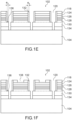
- Lateral etching of part of the dielectric spacer 132 is then carried out, revealing contact surfaces 136 of the second part 123 of the first layer 106 (see Figure 1E ).
- the contact surfaces 136 of the second part 123 of the first layer 106 revealed are preferably substantially horizontal, according to the direction of orientation of the figures. Lateral etching therefore makes it possible to reveal crystalline planes parallel to the growth surface having better electrical properties than planes perpendicular to the growth surface.
- the part of the dielectric spacer 132 which is removed during this lateral etching has a thickness (referenced “e2” on the Figure 1E ) for example between approximately 10 nm and the initial thickness of the spacer (e1) minus approximately 10 nm, so that the remaining thickness of spacer (referenced “e3”) is sufficient to ensure good electrical insulation.
- the thickness e2 is for example equal to approximately 600 nm when the dielectric spacer 132 has an initial thickness e1 equal to approximately 1 ⁇ m.
- Openings 138 are then made through the etching mask 118, forming locations for producing second parts of the second electrodes of the diodes 102 ( figure 1F ). These openings 138 pass through the entire thickness of the engraving mask 118 so that the bottom walls (ie the bottom) of the openings 138 are formed by the portions 124.
- This engraving is for example of the ICP-RIE type.
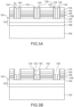
- a first electrically conductive material 140 is then deposited in the trenches 120, as well as on the upper faces of the etching mask 118 and in the openings 138 ( Figure 1G ).
- This first electrically conductive material 140 is deposited in a conformal manner, that is to say by forming a layer of substantially constant thickness on the etching mask 118 and along the walls of the trenches 120 and the openings 138.
- the first electrically conductive material 140 is formed by the deposition of a first layer of titanium with a thickness for example between approximately 5 nm and 300 nm, followed by a deposition of a second layer of aluminum with a thickness for example between approximately 50 nm and 1 ⁇ m.
- the first electrically conductive material 140 is formed by a single layer of aluminum with a thickness for example between approximately 50 nm and 1 ⁇ m.
- the first electrically conductive material 140 deposited is in electrical contact with the lateral flanks of the portions 134 but also with the contact surfaces 136 which actively participate in electrical contact with the semiconductor of the first layer 106 in addition to that with the lateral flanks portions 134.
- the electrically conductive material 140 is also in contact with the portions 124 at the level of the bottom walls (i.e. the bottom) of the openings 138. These electrical contacts are intended to form the electrical connections between the p-n junctions and the anodes and cathodes of diodes 102.
- a second electrically conductive material 142 is deposited by filling the remaining volume of the trenches 120 and the openings 138.
- the thickness of this second electrically conductive material 142 is such that it also covers the parts of the first electrically conductive material 140 arranged on the etching mask 118.
- the second electrically conductive material 142 is for example copper which can be formed by the implementation of a full plate electrochemical deposition (ECD or “Electro-Chemical Deposition”), that is to say on the entire structure previously created.
- the diodes 102 of the device 100 are completed by implementing a chemical-mechanical planarization (CMP) removing the portions of the first and second electrically conductive materials 140 and 142 which protrude from the trenches 120 and the openings 138 and which are arranged on the etching mask 118.
- CMP chemical-mechanical planarization
- This planarization makes it possible to electrically isolate the portions of conductive materials arranged in the trenches 120 from those arranged in the openings 138 ( figure 1I ).
- the portions of the electrically conductive materials 140 and 142 arranged in the trenches 120 form first electrodes 144 (corresponding to cathodes in the exemplary embodiment described here) extending over the entire height of the mesa structures of the diodes 102 and which are connected electrically to the semiconductor portions 134.
- the portions of the electrically conductive materials 140 and 142 arranged in the openings 138 form second parts of the second electrodes 146 (corresponding to anodes in the example described here) electrically connected to the portions 124 corresponding to the first parts of the second electrodes 146.
- the second electrodes 146 are connected to portions 126 at the upper faces of these portions 126.
- This planarization also forms a face 148 of the device 100 which is substantially planar and formed by the upper faces of the electrodes 144, 146, of the dielectric spacer 132 and of the etching mask 118.
- This face 148 forms the rear faces of the diodes 102 at level at which electrical connections with the electrodes 144, 146 will be made.
- the first electrodes 144 are well electrically isolated from the semiconductor portions 124, the second electrodes 146 and the portions 128 forming the active zones of the diodes 102.
- the planarization step can advantageously be implemented until over-etching of the portions of the electrically conductive materials 140 and 142 arranged in the trenches 120 and in the openings 138 relative to the dielectric materials of the dielectric spacer 132 and the etching mask 118, forming hollows in the electrodes 144, 146 at the level of the upper faces of these electrodes.
- These recesses may have a depth, relative to the plane of the upper face 148, of between approximately 5 nm and 150 nm.
- This over-etching can be obtained by playing on the etching selectivity which exists between the dielectric materials of the spacer 132 and the etching mask 118 and the electrically conductive materials 140 and 142.
- the CMP implemented has a speed of different abrasion depending on the materials, and in the process described here, the abrasion of the electrically conductive materials 140 and 142 is faster than that of the dielectric materials of the spacer 132 and the etching mask 118.
- the electrodes 144, 146 of the diodes 102 remain perfectly isolated from each other thanks to to an intrinsic property of the planarization implemented.
- Such over-etching can also be implemented by an RIE etching process.
- the diode matrix 102 is transferred, at its upper face 148, onto an interconnection substrate 150 comprising electrical contacts 152 and 154 to which the electrodes 144, 146 can be electrically connected, for example via direct bonding as described above.
- This interconnection substrate 150 can correspond to an electronic circuit on which the diode matrix 102 is transferred.
- Figures 2A and 2B represent images obtained by electron microscopy during such lateral etching.
- the dielectric spacer 132 is then produced in the trenches 120. Unlike the first embodiment in which the dielectric spacer 132 is produced by depositing a single thick layer of dielectric material, the dielectric spacer 132 is here produced by depositing in a manner conforms a layer 133 of a first dielectric material, this layer 133 covering in particular, in the trenches 120, the side walls of the portions 124, 126, 128 and 130 and of the etching mask 118. A layer 135 of a second dielectric material is then deposited by covering the layer 133.
- the first and second dielectric materials are chosen such that the second dielectric material has an etching speed greater than that of the first dielectric material during the lateral etching of a part of the dielectric spacer which is then implemented, that is to say the anisotropic etching of the spacers and the etching of the semiconductor layers.
- the first dielectric material of layer 133 may correspond to SiO 2 and the second dielectric material of layer 135 may correspond to SiN.
- the difference in etching speed between the first and the second dielectric material during this anisotropic etching results in a difference in height between layer 135 and layer 133 after the fabrication of the dielectric spacer: the remaining portion of layer 135 is less important than the remaining portion of layer 133.
- Another etching is then carried out to extend the trenches 120 to the first substrate 104, through portions of the second part 123 of the first layer 106 which are not covered by the dielectric spacer 132, i.e. that is to say not covered by the portions of layers 133 and 135.
- the trenches 120 also surround remaining portions 134 of the second part 123 of the first layer 106.
- the height of the portions of the layer 135 preserved is adapted depending in particular on the thickness of the etching mask 118, the thicknesses of the different etched layers of semiconductor, or even of the etching selectivity of the different materials, with the aim that throughout the etching extending the trenches, the contact surfaces 136 are well protected by the portions of the layer 135 and that at the end of this etching, the portions of layer 135 are well removed.
- the diodes 102 and the device 100 are then completed as in the first embodiment, by implementing the different steps previously described in connection with the Figures 1F to 1J .
- the semiconductor portions 130, 134 are n-type and the second semiconductor portions 126 are p-type.
- the semiconductor portions 130, 134 may be of p-type and the second semiconductor portions 126 may be of n-type, with in this case the portions of electrically conductive material arranged in the trenches 120 forming the anodes. diodes 102 and the portions of electrically conductive materials arranged in the openings 138 forming, with the portions 124, the cathodes of the diodes 102.
- the device 100 comprises a matrix of diodes 102 which are light-emitting diodes, the microelectronic device 100 being able to form part of an LED display device (screens, projector, video wall, etc.).
- This matrix of diodes 102 comprises the first electrodes 144 which form the same electrode common to all the diodes 102, and each diode 102 comprises a second electrode 146 making it possible to individually address each of the diodes 102.
- the microelectronic device 100 may comprise a matrix of diodes 102 which are photo-receiving diodes, or photodiodes.
- the electrodes 144, 146 do not serve to supply current to the diodes 102 but serve to recover the photocurrents generated by the diodes 102.
- the diodes 102 produced form a matrix of diodes serving as a matrix of pixels of the device 100.
- the diodes 102 can be produced next to each other without forming a matrix of diodes and/or without regular spacing between them.
Description
L'invention concerne le domaine des diodes photo-émettrices ou diodes électroluminescentes (appelées DELs ou LEDs, ou encore micro-LEDs ou µLEDs lorsque leurs dimensions sont de quelques micromètres ou quelques dizaines de micromètres) ainsi que celui des diodes photo-réceptrices ou photodiodes. L'invention s'applique notamment au domaine des dispositifs d'éclairage par LEDs, des dispositifs électroniques émissifs lumineux comprenant des matrices de LEDs tels que des écrans, des projecteurs, des phares de voitures ou des murs d'images, ainsi qu'au domaine des dispositifs électroniques ou microélectroniques photorécepteurs comportant des matrices de photodiodes, tels que des capteurs d'images. L'invention concerne notamment la fabrication de matrices de LEDs ou µLEDs à partir d'empilement de semi-conducteurs GaN/InGaN pour la réalisation d'écrans de visualisation ou d'éclairage matriciel.The invention relates to the field of photo-emitting diodes or light-emitting diodes (called LEDs or LEDs, or micro-LEDs or µLEDs when their dimensions are a few micrometers or a few tens of micrometers) as well as that of photo-receiving diodes or photodiodes. . The invention applies in particular to the field of LED lighting devices, luminous emissive electronic devices comprising matrices of LEDs such as screens, projectors, car headlights or video walls, as well as to field of electronic or microelectronic photoreceptor devices comprising photodiode matrices, such as image sensors. The invention relates in particular to the manufacture of matrices of LEDs or µLEDs from stacks of GaN/InGaN semiconductors for the production of display screens or matrix lighting.
La réalisation de diodes, par exemple lors de la réalisation d'une matrice de photodiodes ou de LEDs formant une matrice de pixels, se base généralement sur la mise en oeuvre de procédés microélectroniques standards utilisés communément en technologie dite planaire et au cours desquels chaque élément des diodes est réalisé par une étape de dépôt, puis une étape de lithographie suivie d'une étape de gravure. Avec ce type de procédé, la réalisation de chaque motif d'un matériau des diodes nécessite la mise en oeuvre d'au moins trois étapes distinctes. De plus, chaque motif réalisé doit être aligné avec ceux précédemment réalisés. Enfin, la définition de chaque motif doit prendre en compte les performances des équipements concernés tant en termes de dimensions atteignables que de performances d'alignement par rapport au motif précédent.The production of diodes, for example when producing a matrix of photodiodes or LEDs forming a matrix of pixels, is generally based on the implementation of standard microelectronic processes commonly used in so-called planar technology and during which each element diodes is produced by a deposition step, then a lithography step followed by an etching step. With this type of process, the production of each pattern of a diode material requires the implementation of at least three distinct steps. In addition, each pattern made must be aligned with those previously made. Finally, the definition of each pattern must take into account the performance of the equipment concerned both in terms of achievable dimensions and alignment performance compared to the previous pattern.
De plus, pour obtenir des performances suffisantes avec les technologies standards de la micro-électronique, une planarisation des éléments réalisés est nécessaire afin de maîtriser les étapes de lithographie mises en oeuvre sur ces éléments car la résolution atteignable avec une étape de lithographie est directement liée à la topographie sur laquelle cette lithographie est mise en oeuvre, les objectifs optiques à très grandes ouvertures utilisés dans les dispositifs d'insolation lithographiques ayant des profondeurs de champ qui s'amenuisent avec l'augmentation de la résolution.In addition, to obtain sufficient performance with standard microelectronics technologies, planarization of the elements produced is necessary in order to master the lithography steps implemented on these elements because the resolution achievable with a lithography step is directly linked to the topography on which this lithography is implemented, the optical objectives with very large apertures used in the devices lithographic exposures having depths of field which diminish with increasing resolution.
Le document
Cependant, du point de vue électrique, il est préférable que le contact électrique entre le semi-conducteur de la partie dopée N ou P se trouvant sur le substrat et les électrodes assurant l'isolation optique ne se fasse pas au niveau des flancs latéraux de cette partie mais par exemple au niveau d'une surface parallèle au substrat, en raison des meilleures propriétés électriques des plans cristallins parallèles à la surface de croissance. Cela permet l'obtention d'une meilleure réponse électrique, c'est-à-dire un courant électrique plus important pour une même tension de fonctionnement, et donc, dans le cas des diodes photo-émettrices, une plus grande quantité de lumière émise pour une même puissance électrique injectée. Par contre, réaliser le contact électrique au niveau d'une surface parallèle au substrat implique de ne pas graver le semi-conducteur jusqu'au substrat pour en conserver une partie au fond des tranchées, ce qui dégrade l'isolation optique entre les pixels, c'est-à-dire augmente la diaphonie entre les pixels. Cela est décrit dans le document "
Un compromis doit donc être réalisé entre l'isolation optique des pixels et la réponse électrique obtenues.A compromise must therefore be made between the optical isolation of the pixels and the electrical response obtained.
Dans le document
Un but de la présente invention est de proposer une diode dont la structure permet de concilier une bonne isolation optique entre pixels et une bonne réponse électrique des pixels, et qui puisse être réalisée de manière auto-alignée et sans dégradation de ses propriétés électriques.An aim of the present invention is to propose a diode whose structure makes it possible to reconcile good optical insulation between pixels and a good electrical response of the pixels, and which can be produced in a self-aligned manner and without degradation of its electrical properties.
Pour cela, la présente invention propose, conformément à la revendication indépendante 1 en annexe, un procédé de réalisation d'au moins une diode photo-émettrice ou photo-réceptrice, comportant au moins :
- réalisation, sur un premier substrat, d'au moins un empilement comprenant des première et deuxième couches de semi-conducteur dopées selon des types de conductivité opposés, et au moins une troisième couche de semi-conducteur intrinsèque, ou semi-conducteur non intentionnellement dopé, disposée entre les première et deuxième couches, la première couche étant disposée entre le premier substrat et la troisième couche ;
- gravure de tranchées traversant les deuxième et troisième couches et une première partie de la première couche, entourant des portions restantes des deuxième et troisième couches et de la première partie de la première couche, et telles que le fond des tranchées soit formé par une deuxième partie de la première couche disposée entre la première partie de la première couche et le premier substrat ;
- réalisation, dans les tranchées, d'au moins un espaceur diélectrique recouvrant des parois latérales desdites portions restantes ;
- gravure prolongeant les tranchées à travers des portions de la deuxième partie de la première couche non recouvertes par l'espaceur diélectrique, jusqu'au premier substrat ;
- gravure latérale d'une partie de l'espaceur diélectrique, révélant des surfaces de contact, par exemple horizontales, de la deuxième partie de la première couche ;
- réalisation, dans les tranchées, d'au moins une première électrode en contact avec les surfaces de contact de la deuxième partie de la première couche et avec des flancs latéraux de la deuxième partie de la première couche.
- production, on a first substrate, of at least one stack comprising first and second semiconductor layers doped according to opposite types of conductivity, and at least one third semiconductor layer intrinsic, or non-intentionally doped semiconductor, disposed between the first and second layers, the first layer being disposed between the first substrate and the third layer;
- etching of trenches crossing the second and third layers and a first part of the first layer, surrounding remaining portions of the second and third layers and the first part of the first layer, and such that the bottom of the trenches is formed by a second part of the first layer disposed between the first part of the first layer and the first substrate;
- production, in the trenches, of at least one dielectric spacer covering the side walls of said remaining portions;
- etching extending the trenches through portions of the second part of the first layer not covered by the dielectric spacer, to the first substrate;
- lateral etching of a part of the dielectric spacer, revealing contact surfaces, for example horizontal, of the second part of the first layer;
- production, in the trenches, of at least one first electrode in contact with the contact surfaces of the second part of the first layer and with lateral flanks of the second part of the first layer.
Des modes avantageux de réalisation de la présente invention sont l'objet des revendications dépendantes en annexe.Advantageous embodiments of the present invention are the subject of the appended dependent claims.
Du fait que la première électrode se prolonge jusqu'au premier substrat, l'isolation optique de la diode est très efficace. Lorsque cette diode forme un pixel comprenant des pixels voisins, une bonne isolation optique entre pixels est donc obtenue, ce qui permet d'éviter les interactions lumineuses entre les diodes voisines.Because the first electrode extends to the first substrate, the optical isolation of the diode is very effective. When this diode forms a pixel comprising neighboring pixels, good optical isolation between pixels is therefore obtained, which makes it possible to avoid light interactions between neighboring diodes.
De plus, du fait que la première électrode est reliée électriquement au semi-conducteur de la portion restante de la première couche par l'intermédiaire des parois latérales de la deuxième partie de la première couche et par l'intermédiaire des surfaces de contact formées par la gravure latérale de l'espaceur diélectrique, une bonne réponse électrique de la diode est également obtenue.Furthermore, due to the fact that the first electrode is electrically connected to the semiconductor of the remaining portion of the first layer via the side walls of the second part of the first layer and via the contact surfaces formed by side etching of the dielectric spacer, good electrical response of the diode is also obtained.
Cette diode fait appel à un espaceur diélectrique, c'est-à-dire un élément d'isolation électrique, recouvrant les flancs latéraux d'une partie des éléments formant la jonction p-n de la diode et permettant d'isoler électriquement et de passiver ces flancs latéraux, notamment vis-à-vis de la première électrode, et également d'isoler électriquement les portions de semi-conducteur dopées de la jonction p-n l'une vis-à-vis de l'autre. Cet espaceur diélectrique permet également d'assurer l'isolation électrique entre la première électrode et la deuxième électrode en occupant un minimum de place dans la diode. Cette localisation de l'espaceur diélectrique sur les flancs latéraux de la jonction p-n de la diode permet d'améliorer le rapport entre la surface active de la diode (surface occupée par la jonction p-n) et la surface totale occupée par la diode, et donc de réduire son encombrement.This diode uses a dielectric spacer, that is to say an electrical insulation element, covering the lateral sides of part of the elements forming the p-n junction of the diode and making it possible to electrically isolate and passivate these lateral flanks, in particular with respect to the first electrode, and also to electrically isolate the doped semiconductor portions of the p-n junction from each other. This dielectric spacer also makes it possible to ensure electrical insulation between the first electrode and the second electrode by occupying a minimum of space in the diode. This location of the dielectric spacer on the lateral sides of the p-n junction of the diode makes it possible to improve the ratio between the active surface of the diode (surface occupied by the p-n junction) and the total surface occupied by the diode, and therefore to reduce its size.
De plus, cette forte intégration de l'espaceur diélectrique a également pour avantage de minimiser les densités de courant obtenues dans les électrodes de la diode, et donc de réduire l'échauffement par effet Joule engendré dans la diode via une baisse globale de la résistance thermique de la diode.In addition, this strong integration of the dielectric spacer also has the advantage of minimizing the current densities obtained in the electrodes of the diode, and therefore of reducing the heating by Joule effect generated in the diode via an overall reduction in resistance. thermal of the diode.
La structure de cette diode permet de réduire son coût de fabrication ainsi que sa consommation d'énergie. Dans le domaine de l'éclairage, une telle diode permet d'améliorer l'injection électrique obtenue et donc d'augmenter son rendement énergétique. Dans le domaine des dispositifs imageurs, une telle diode permet de réaliser des dispositifs à haute résolution par la réduction de la taille des pixels qui devient limitée uniquement par les moyens de mise en forme utilisés.The structure of this diode makes it possible to reduce its manufacturing cost as well as its energy consumption. In the field of lighting, such a diode makes it possible to improve the electrical injection obtained and therefore to increase its energy efficiency. In the field of imaging devices, such a diode makes it possible to produce high resolution devices by reducing the size of the pixels which becomes limited only by the shaping means used.
Le terme « couche » est utilisé, ici et dans tout le reste du document, pour désigner une seule couche ou un empilement de plusieurs couches.The term “layer” is used, here and throughout the rest of the document, to refer to a single layer or a stack of several layers.
La jonction p-n formée et l'espaceur diélectrique forment une structure mesa. L'expression « structure mesa » désigne le fait que la diode est réalisée sous la forme d'un empilement de portions de semi-conducteur dopées, une zone de jonction à base de semi-conducteur intrinsèque étant présente entre ces portions de semi-conducteur dopées, et que cet empilement est ici gravé sur toute sa hauteur sous forme d'un îlot appelé mesa.The formed p-n junction and the dielectric spacer form a mesa structure. The expression “mesa structure” designates the fact that the diode is produced in the form of a stack of doped semiconductor portions, a junction zone based on intrinsic semiconductor being present between these semiconductor portions doped, and that this stack is here engraved over its entire height in the form of an island called a mesa.
Les parois de fond (i.e. les fonds) des tranchées peuvent être horizontales.The bottom walls (ie the bottoms) of the trenches can be horizontal.
L'espaceur diélectrique étant déposé sur les flancs latéraux de la structure gravée dans l'empilement de couches, cet espaceur diélectrique peut être réalisé par un procédé auto-aligné permettant d'isoler les électrodes de la diode sans faire appel à un masque spécialement adapté à la réalisation de cet espaceur diélectrique, par exemple via un dépôt conforme du matériau de l'espaceur diélectrique puis une gravure, par exemple anisotrope, des portions de ce matériau diélectrique qui ne recouvrent pas les flancs latéraux de la structure.The dielectric spacer being deposited on the lateral sides of the structure etched in the stack of layers, this dielectric spacer can be produced by a self-aligned process making it possible to isolate the electrodes of the diode without using a specially adapted mask to the production of this dielectric spacer, for example via a conformal deposition of the material of the dielectric spacer then an etching, for example anisotropic, of the portions of this dielectric material which do not cover the lateral sides of the structure.
La première couche de semi-conducteur peut être dopée n et la deuxième couche de semi-conducteur peut être dopée p, la première électrode pouvant dans ce cas former une cathode de la diode.The first semiconductor layer may be n-doped and the second semiconductor layer may be p-doped, the first electrode being able in this case to form a cathode of the diode.
La diode réalisée peut comporter, du côté opposé à celui où se trouve le premier substrat, une surface continue sensiblement plane. Cette surface continue sensiblement plane permet d'hybrider facilement, par exemple sans faire appel à des inserts tels que des microbilles de connexion, la diode à un autre élément tel qu'un substrat permettant de réaliser différentes configurations de connexion de la diode et pouvant comporter également une face plane au niveau de laquelle se trouvent des matériaux analogues à ceux de la diode, par exemple par collage direct métal contre métal (pour les électrodes) et diélectrique contre diélectrique (notamment pour l'espaceur diélectrique). Cette surface continue sensiblement plane est également bien adaptée pour la réalisation d'une structure d'interconnexions directement sur les électrodes, évitant ainsi bon nombre de difficultés liées à la topologie résiduelle des structures des diodes de l'art antérieur.The diode produced may comprise, on the side opposite to that where the first substrate is located, a substantially flat continuous surface. This substantially flat continuous surface makes it possible to easily hybridize, for example without using inserts such as connection microbeads, the diode to another element such as a substrate making it possible to produce different connection configurations of the diode and which may include also a flat face at which there are materials similar to those of the diode, for example by direct bonding metal to metal (for the electrodes) and dielectric to dielectric (in particular for the dielectric spacer). This substantially flat continuous surface is also well suited for producing an interconnection structure directly on the electrodes, thus avoiding a number of difficulties linked to the residual topology of the diode structures of the prior art.
L'expression « sensiblement plane » est ici utilisée pour désigner le fait que la surface ainsi formée peut présenter des variations de hauteur, ou d'épaisseur, comprises entre environ 0 et 150 nm. Ces légères variations de hauteur ou d'épaisseur peuvent avoir pour origine la mise en oeuvre d'une planarisation mécano-chimique (CMP) mise en oeuvre en présence des matériaux des électrodes et des matériaux diélectriques, les vitesses de gravure de ces différents matériaux étant différentes les unes des autres. Ces légères variations de hauteur ou d'épaisseur peuvent avoir pour avantage de garantir une excellente isolation entre les électrodes de la diode et/ou vis-à-vis d'électrodes de diodes adjacentes lorsque des creux sont formés au niveau des faces supérieures des électrodes.The expression “substantially planar” is used here to designate the fact that the surface thus formed can have variations in height, or thickness, of between approximately 0 and 150 nm. These slight variations in height or thickness may originate from the implementation of a mechanical-chemical planarization (CMP) implemented in the presence of the electrode materials and dielectric materials, the etching speeds of these different materials being different from each other. These slight variations in height or thickness can have the advantage of guaranteeing excellent insulation between the electrodes of the diode and/or with respect to electrodes of adjacent diodes when hollows are formed at the upper faces of the electrodes.
La première couche de semi-conducteur peut comporter un empilement d'au moins deux semi-conducteurs dopés selon des niveaux de conductivité différents. Par exemple, lorsque la première couche de semi-conducteur est dopée n, elle peut comporter un empilement d'un premier semi-conducteur dopé n+ disposé sur le premier substrat et d'un deuxième semi-conducteur dopé n- disposé sur le premier semi-conducteur.The first semiconductor layer may comprise a stack of at least two semiconductors doped at different conductivity levels. For example, when the first semiconductor layer is n-doped, it may comprise a stack of a first n+-doped semiconductor placed on the first substrate and a second n--doped semiconductor placed on the first semiconductor. -driver.
La diode peut être une photodiode ou une LED. Lorsque la diode est une LED, elle peut comporter plusieurs troisièmes couches de semi-conducteur intrinsèque formant une zone active émissive à au moins un puits quantique disposée entre les semi-conducteurs des première et deuxième couches.The diode can be a photodiode or an LED. When the diode is an LED, it may comprise several third layers of intrinsic semiconductor forming an active emissive zone with at least one quantum well arranged between the semiconductors of the first and second layers.
La gravure latérale mise en oeuvre ici correspond à une gravure réduisant l'épaisseur d'au moins une partie de l'espaceur diélectrique.The lateral etching implemented here corresponds to an etching reducing the thickness of at least part of the dielectric spacer.
L'espaceur diélectrique peut avoir, avant la mise en oeuvre de la gravure latérale, une épaisseur initiale supérieure ou égale à 1 µm.The dielectric spacer may have, before carrying out lateral etching, an initial thickness greater than or equal to 1 µm.
La partie de l'espaceur diélectrique supprimée lors de la gravure latérale peut avoir une épaisseur comprise entre 10 nm et une épaisseur initiale de l'espaceur moins 10 nm, afin que l'épaisseur restante d'espaceur soit suffisante pour assurer une bonne isolation électrique.The portion of the dielectric spacer removed during side etching may have a thickness between 10 nm and an initial spacer thickness minus 10 nm, so that the remaining spacer thickness is sufficient to provide good electrical insulation .
Les surfaces de contact de la deuxième partie de la première couche peuvent être perpendiculaires aux parois latérales desdites portions restantes.The contact surfaces of the second part of the first layer can be perpendicular to the side walls of said remaining portions.
Le procédé peut comporter en outre, entre la réalisation de l'empilement et la gravure des tranchées à travers les deuxième et troisième couches et la première partie de la première couche, la réalisation d'au moins un masque de gravure disposé sur l'empilement et ayant un motif correspondant à celui des tranchées, et l'espaceur diélectrique peut être réalisé en recouvrant également des parois latérales du masque de gravure.The method may further comprise, between the production of the stack and the etching of the trenches through the second and third layers and the first part of the first layer, the production of at least one etching mask placed on the stack and having a pattern corresponding to that of the trenches, and the dielectric spacer can be made by also covering side walls of the etching mask.
Dans un premier mode de réalisation, la gravure latérale d'une partie de l'espaceur diélectrique correspond à une gravure isotrope.In a first embodiment, the lateral etching of a part of the dielectric spacer corresponds to isotropic etching.
Le masque de gravure peut comporter au moins un matériau qui est au moins partiellement gravé lors de la gravure latérale d'une partie de l'espaceur diélectrique.The etch mask may include at least one material that is at least partially etched during side etching of a portion of the dielectric spacer.
L'espaceur diélectrique peut comporter du SiO2.The dielectric spacer may comprise SiO 2 .
Dans un deuxième mode de réalisation, la réalisation de l'espaceur diélectrique peut comporter :
- dépôt d'au moins une couche d'un premier matériau diélectrique recouvrant les parois latérales desdites portions restantes ;
- dépôt d'au moins une couche d'un deuxième matériau diélectrique recouvrant la couche du premier matériau diélectrique, le deuxième matériau diélectrique étant choisi tel qu'il ait une vitesse de gravure supérieure à celle du premier matériau diélectrique lors de la gravure latérale d'une partie de l'espaceur diélectrique qui correspond à une gravure anisotrope ;
- depositing at least one layer of a first dielectric material covering the side walls of said remaining portions;
- deposition of at least one layer of a second dielectric material covering the layer of the first dielectric material, the second dielectric material being chosen such that it has an etching speed greater than that of the first dielectric material during the lateral etching of a part of the dielectric spacer which corresponds to anisotropic etching;
Le procédé peut être tel que :
- l'empilement comporte en outre au moins une couche électriquement conductrice telle que la deuxième couche soit disposée entre la troisième couche et la couche électriquement conductrice (cette couche électriquement conductrice peut être disposée entre la deuxième couche et un masque de gravure lorsqu'un masque de gravure est utilisé) ;
- les tranchées gravées traversent la couche électriquement conductrice et entourent au moins une portion restante de la couche électriquement conductrice formant une première partie d'une deuxième électrode ;
- l'espaceur diélectrique recouvre des parois latérales de la première partie de la deuxième électrode ;
- the stack further comprises at least one electrically conductive layer such that the second layer is placed between the third layer and the electrically conductive layer (this electrically conductive layer can be placed between the second layer and an etching mask when a mask of engraving is used);
- the etched trenches pass through the electrically conductive layer and surround at least a remaining portion of the electrically conductive layer forming a first part of a second electrode;
- the dielectric spacer covers side walls of the first part of the second electrode;
Dans ce cas, la réalisation de la première électrode et de la deuxième partie de la deuxième électrode peut comporter au moins :
- réalisation d'au moins une ouverture à travers l'empilement et débouchant sur la première partie de la deuxième électrode ;
- dépôt d'au moins un matériau électriquement conducteur dans l'ouverture et dans les tranchées ;
- planarisation du matériau électriquement conducteur.
- production of at least one opening through the stack and opening onto the first part of the second electrode;
- depositing at least one electrically conductive material in the opening and in the trenches;
- planarization of the electrically conductive material.
Dans ce cas, la réalisation des électrodes correspond à la mise en oeuvre d'un procédé de type « damascène » dans lequel un ou plusieurs matériaux électriquement conducteurs sont formés par au moins un dépôt pleine plaque, c'est-à-dire un dépôt du matériau électriquement conducteur sur l'ensemble de la structure réalisée, les électrodes étant obtenues ensuite via une planarisation de ce ou ces matériaux électriquement conducteurs. La réalisation de la première électrode ne nécessite donc pas une étape d'alignement spécifique ou de masquage particulier. L'emplacement de la première électrode peut correspondre à un espace formé par les tranchées entre des diodes voisines.In this case, the production of the electrodes corresponds to the implementation of a “Damascene” type process in which one or more electrically conductive materials are formed by at least one full plate deposition, that is to say a deposition electrically conductive material over the entire structure produced, the electrodes then being obtained via planarization of this or these electrically conductive materials. The production of the first electrode therefore does not require a specific alignment or particular masking step. The location of the first electrode may correspond to a space formed by the trenches between neighboring diodes.
Le procédé peut comporter en outre, après la réalisation de la première électrode et de la deuxième partie de la deuxième électrode, un report de la diode photo-émettrice ou photo-réceptrice sur un substrat d'interconnexions tel que les première et deuxième électrodes de la diode photo-émettrice ou photo-réceptrice soient reliées électriquement au substrat d'interconnexions, puis une étape de retrait du premier substrat.The method may further comprise, after the production of the first electrode and the second part of the second electrode, a transfer of the photo-emitting or photo-receiving diode onto an interconnection substrate such as the first and second electrodes of the photo-emitting or photo-receiving diode are electrically connected to the interconnection substrate, then a step of removing the first substrate.
La couche électriquement conductrice peut être optiquement réflectrice, c'est-à-dire peut présenter un coefficient de réflexion en amplitude (rapport de l'amplitude de la lumière réfléchie sur l'amplitude de la lumière incidente) d'au moins 80 %. Dans ce cas, la deuxième électrode, qui est disposée du côté opposé à celui par lequel la lumière est destinée à entrer ou sortir de la diode, peut être optiquement réflectrice. Ainsi, la lumière peut entrer ou sortir de la diode sans avoir à traverser une électrode transparente, par exemple à base d'un oxyde transparent conducteur tel que l'ITO, qui engendre des pertes optiques de la lumière émise ou reçue.The electrically conductive layer can be optically reflective, that is to say it can have an amplitude reflection coefficient (ratio of the amplitude of the reflected light to the amplitude of the incident light) of at least 80%. In this case, the second electrode, which is arranged on the side opposite to that through which the light is intended to enter or exit the diode, can be optically reflector. Thus, light can enter or leave the diode without having to pass through a transparent electrode, for example based on a transparent conductive oxide such as ITO, which generates optical losses in the light emitted or received.
L'invention concerne également, conformément à la revendication 14 en annexe, un procédé de réalisation d'un dispositif électronique, comportant la mise en oeuvre d'un procédé tel que décrit ci-dessus, dans lequel les étapes mises en oeuvre forment plusieurs diodes photo-émettrices et/ou plusieurs diodes photo-réceptrices dans lesquelles les premières électrodes desdites diodes sont reliées électriquement entre elles.The invention also relates, in accordance with claim 14 in the appendix, to a method of producing an electronic device, comprising the implementation of a method as described above, in which the steps implemented form several diodes photo-emitting diodes and/or several photo-receiving diodes in which the first electrodes of said diodes are electrically connected together.
Selon une configuration particulière, les premières électrodes des diodes du dispositif peuvent former une cathode commune à ces diodes.According to a particular configuration, the first electrodes of the diodes of the device can form a cathode common to these diodes.
Les diodes peuvent faire partie d'une matrice de diodes de structures similaires formant une matrice de pixels du dispositif électronique.The diodes may be part of a matrix of diodes of similar structures forming a matrix of pixels of the electronic device.
La présente invention sera mieux comprise à la lecture de la description d'exemples de réalisation donnés à titre purement indicatif et nullement limitatif en faisant référence aux dessins annexés sur lesquels :
- les
figures 1A à 1J représentent les étapes d'un procédé, selon la présente invention, de réalisation d'un dispositif électronique, incluant un procédé, également selon la présente invention, de réalisation d'une diode photo-émissive ou photo-réceptrice, selon un premier mode de réalisation de la présente invention; - les
figures 2A et 2B représentent des photos d'une structure obtenue lors de la mise en oeuvre d'une gravure latérale isotrope d'un masque de gravure similaire à celle mise en oeuvre au cours du procédé, selon la présente invention, de réalisation d'une diode photo-émissive ou photo-réceptrice, selon le premier mode de réalisation ; - les
figures 3A et 3B représentent une partie des étapes d'un procédé , selon la présente invention, de réalisation d'un dispositif électronique, incluant un procédé, également selon la présente invention, de réalisation d'une diode photo-émissive ou photo-réceptrice, selon un deuxième mode de réalisation de la présente invention.
- THE
Figures 1A to 1J represent the steps of a method, according to the present invention, for producing an electronic device, including a method, also according to the present invention, for producing a photo-emitting or photo-receiving diode, according to a first mode of carrying out the present invention; - THE
Figures 2A and 2B represent photos of a structure obtained during the implementation of an isotropic lateral etching of an etching mask similar to that implemented during the process, according to the present invention, for producing a photodiode. emissive or photo-receptive, according to the first embodiment; - THE
Figures 3A and 3B represent part of the steps of a method, according to the present invention, for producing an electronic device, including a method, also according to the present invention, for producing a photo-emitting or photo-receiving diode, according to a second embodiment of the present invention.
Des parties identiques, similaires ou équivalentes des différentes figures décrites ci-après portent les mêmes références numériques de façon à faciliter le passage d'une figure à l'autre.Identical, similar or equivalent parts of the different figures described below bear the same numerical references so as to facilitate the transition from one figure to another.
Les différentes parties représentées sur les figures ne le sont pas nécessairement selon une échelle uniforme, pour rendre les figures plus lisibles.The different parts represented in the figures are not necessarily on a uniform scale, to make the figures more readable.
Les différentes possibilités (variantes et modes de réalisation de la présente invention) doivent être comprises comme n'étant pas exclusives les unes des autres et peuvent se combiner entre elles, tant que ces combinaisons demeurent dans le cadre de l'étendue de la présente invention telle que définie par les revendications en annexe.The different possibilities (variants and embodiments of the present invention) must be understood as not being exclusive of each other and can be combined with each other, as long as these combinations remain within the scope of the present invention. as defined by the appended claims.
Les
Comme représenté sur la
Une première couche 106 de semi-conducteur dopé selon un premier type de conductivité, par exemple de type n, est réalisée sur le premier substrat 104.A
Selon un exemple de réalisation particulier, cette première couche 106 correspond à un empilement de plusieurs couches distinctes de semi-conducteur, par exemple une couche 108 de semi-conducteur dopée n+ avec une concentration de donneurs par exemple comprise entre environ 5.1017 et 5.1020 donneurs/cm3 sur laquelle est disposée une autre couche 110 de semi-conducteur dopée n- avec une concentration de donneurs par exemple comprise entre environ 1017 et 5.1019 donneurs/cm3. Par exemple, la couche 108 peut comporter du GaN et la couche 110 peut comporter de l'InGaN. L'épaisseur de la couche 108 est par exemple supérieure à environ 100 nm, par exemple égale à environ 3 µm, et celle de la couche 110 est par exemple comprise entre environ 5 nm et 500 nm. L'épaisseur totale de la première couche 106, c'est-à-dire la somme des épaisseurs des couches 108 et 110 dans cet exemple de réalisation particulier, est par exemple comprise entre environ 20 nm et 10 µm, et de préférence comprise entre environ 2 µm et 4 µm. La couche 108 forme ici une couche tampon disposée entre la couche 110 et le premier substrat 104 et sert notamment à filtrer les défauts de croissance afin que ces défauts ne se retrouvent pas dans la couche 110 qui sert à former les jonctions p-n des diodes 102.According to a particular embodiment, this
En variante, les couches 108 et 110 peuvent être dopées avec un même niveau de dopage.Alternatively, layers 108 and 110 can be doped with the same doping level.
Selon une autre variante, la couche 106 peut correspondre à une seule couche de semi-conducteur. Cette unique couche de semi-conducteur est par exemple dopée n et peut avoir une concentration de donneurs par exemple comprise entre environ 1017 et 5.1020 donneurs/cm3. A titre d'exemple, cette couche peut comporter du GaN et son épaisseur est par exemple comprise entre environ 20 nm et 10 µm, et avantageusement comprise entre environ 2 µm et 4 µm.According to another variant,
Selon une autre variante, la couche 106 peut correspondre à un empilement de plusieurs couches distinctes de semi-conducteur, par exemple une couche 108 de semi-conducteur non dopé intentionnellement et formant une couche tampon disposée entre la couche 110 et le premier substrat 104, sur laquelle est disposée la couche 110 de semi-conducteur dopée n avec une concentration de donneurs par exemple comprise entre environ 1017 et 5.1020 donneurs/cm3. L'épaisseur de la couche 108 est par exemple supérieure à environ 100 nm, par exemple égale à environ 3 µm, et celle de la couche 110 est par exemple comprise entre environ 100 nm et 3 µm.According to another variant, the
Une ou plusieurs troisièmes couches 112 de semi-conducteur intrinsèque, c'est-à-dire non dopé intentionnellement (de concentration en donneurs résiduels nnid par exemple égale à environ 1017 donneurs/cm3, ou comprise entre environ 1015 et 1018 donneurs/cm3), sont réalisées sur la première couche 106 (sur la couche 110 dans l'exemple représenté sur la
Une deuxième couche 114 de semi-conducteur dopé selon un deuxième type de conductivité, opposé à celui du dopage de la première couche 106 et donc ici de type p, avec une concentration d'accepteurs par exemple comprise entre environ 1017 et 5.1019 accepteurs/cm3, est réalisée sur la ou les troisièmes couches 112. Les couches 106, 112 et 114 (et plus particulièrement les couches 110, 112 et 114 dans l'exemple décrit ici) sont destinées à former les jonctions p-i-n des diodes 102. Le semi-conducteur de la deuxième couche 114 est par exemple du GaN et son épaisseur est par exemple comprise entre environ 20 nm et 10 µm.A
Dans une variante de réalisation, une couche de blocage d'électrons (non visible sur les
Des matériaux autres que ceux cités ci-dessus peuvent être utilisés pour réaliser les couches 106, 112 et 114. Par exemple, le matériau des couches émissives formées par les troisièmes couches 112 est choisi en fonction du spectre d'émission souhaité des diodes 102.Materials other than those mentioned above can be used to produce
Une couche électriquement conductrice 115 destinée à former, dans chaque diode 102, une première partie d'une deuxième électrode qui sera en contact avec le semi-conducteur de la deuxième couche 114, est disposée sur la deuxième couche 114. Le matériau électriquement conducteur utilisé est avantageusement optiquement réflecteur, et correspond par exemple à de l'aluminium ou de l'argent.An electrically
Une couche 116 destinée à former un masque de gravure est réalisée sur la couche 115. Le matériau de cette couche 116 est par exemple du SiO2.A
Les couches 106, 112, 114 et 115 forment ensemble un empilement 117 à partir duquel les diodes 102 vont être réalisées.The
Comme représenté sur la
Une gravure de tranchées 120 traversant la couche électriquement conductrice 115, la deuxième couche 114, la ou les troisièmes couches 112 et une première partie 122 de la première couche 106 est mise en oeuvre selon le motif du masque de gravure 118. Cette gravure est stoppée à un niveau de profondeur situé dans la première couche 106 telle qu'une deuxième partie 123 de la première couche 106 soit conservée au fond de chacune des tranchées 120 gravées. Sur la
A l'issue de cette gravure, les tranchées 120 entourent :
- le masque de gravure 118 ;
- des portions restantes 124 de la couche électriquement conductrice 115 destinées à former des premières parties des deuxièmes électrodes des
diodes 102, - des portions restantes 126 de la deuxième couche 114 destinées à faire partie des jonctions p-n des
diodes 102, - des portions restantes 128 de la ou des troisièmes
couches 112 destinées à former les zones actives de chaquediode 102, et - des portions restantes 130 de la première partie 122 de la première couche 106 destinées à former, avec les portions restantes 126 de la deuxième couche 114, les jonctions p-n des
diodes 102.
- the
engraving mask 118; - remaining
portions 124 of the electricallyconductive layer 115 intended to form first parts of the second electrodes of thediodes 102, - remaining
portions 126 of thesecond layer 114 intended to form part of the pn junctions of thediodes 102, - remaining
portions 128 of the third layer(s) 112 intended to form the active zones of eachdiode 102, and - remaining
portions 130 of thefirst part 122 of thefirst layer 106 intended to form, with the remainingportions 126 of thesecond layer 114, the pn junctions of thediodes 102.
Les couches 115, 112, 114 et 106 sont gravées par voie sèche, par exemple par une gravure ionique réactive mise en oeuvre avec un système de torche à plasma, ou ICP-RIE pour « Inductively Coupled Plasma - Reactive Ion Etching ».
Un espaceur diélectrique 132 est ensuite réalisé dans les tranchées 120 (voir
L'espaceur diélectrique 132 a une épaisseur initiale égale à celle de la couche diélectrique déposée. Cette épaisseur est importante et par exemple supérieure ou égale à environ 1 µm.Sur la
Comme représenté sur la
Le masque de gravure 118, les portions restantes 124, 126, 128, 130, 134 et l'espaceur diélectrique 132 forment des structures mesa, c'est-à-dire des empilements sous forme d'îlots, disposées sur le premier substrat 104. Chaque structure mesa de chaque diode 102 a une section, dans un plan parallèle à la face du premier substrat 104 sur laquelle reposent ces structures, par exemple de forme rectangulaire. Chacune des structures mesa peut donc former un îlot de forme parallélépipédique. Des structures mesa de forme différente sont possibles, par exemple cylindriques.The
Une gravure latérale d'une partie de l'espaceur diélectrique 132 est ensuite mise en oeuvre, révélant des surfaces de contact 136 de la deuxième partie 123 de la première couche 106 (voir
Dans ce premier mode de réalisation, la gravure latérale de l'espaceur diélectrique 132 mise en oeuvre correspond à une gravure isotrope, par exemple une gravure chimique par voie humide ou une gravure plasma isotrope. Lors d'une telle gravure isotrope, le masque de gravure 118 est donc également au moins partiellement gravé si le matériau du masque de gravure 118 est sensible aux agents de gravure utilisés (c'est le cas dans l'exemple de réalisation décrit ici où le masque de gravure 118 et l'espaceur diélectrique 132 comportent du SiO2).In this first embodiment, the lateral etching of the
Des ouvertures 138 sont ensuite réalisées à travers le masque de gravure 118, formant des emplacements pour la réalisation de deuxièmes parties des deuxièmes électrodes des diodes 102 (
Un premier matériau électriquement conducteur 140 est ensuite déposé dans les tranchées 120, ainsi que sur les faces supérieures du masque de gravure 118 et dans les ouvertures 138 (
Le premier matériau électriquement conducteur 140 déposé est en contact électriquement avec les flancs latéraux des portions 134 mais également avec les surfaces de contact 136 qui participent activement au contact électrique avec le semi-conducteur de la première couche 106 en complément de celui avec les flancs latéraux des portions 134. Le matériau électriquement conducteur 140 est également en contact avec les portions 124 au niveau des parois de fond (i.e. du fond) des ouvertures 138. Ces contacts électriques sont destinés à former les liaisons électriques entre les jonctions p-n et les anodes et cathodes des diodes 102.The first electrically
Comme représenté sur la
Enfin, les diodes 102 du dispositif 100 sont achevées en mettant en oeuvre une planarisation mécano-chimique (CMP) supprimant les portions des premier et deuxième matériaux électriquement conducteurs 140 et 142 qui dépassent des tranchées 120 et des ouvertures 138 et qui sont disposées sur le masque de gravure 118. Cette planarisation permet d'isoler électriquement les portions de matériaux conducteurs disposées dans les tranchées 120 vis-à-vis de celles disposées dans les ouvertures 138 (
Cette planarisation forme également une face 148 du dispositif 100 qui est sensiblement plane et formée par les faces supérieures des électrodes 144, 146, de l'espaceur diélectrique 132 et du masque de gravure 118. Cette face 148 forme les faces arrière des diodes 102 au niveau desquelles des connexions électriques avec les électrodes 144, 146 seront réalisées.This planarization also forms a
Grâce à l'espaceur diélectrique 132, les premières électrodes 144 sont bien isolées électriquement des portions de semi-conducteur 124, des deuxièmes électrodes 146 et des portions 128 formant les zones actives des diodes 102.Thanks to the
Afin de garantir une isolation électrique entre les électrodes 144, 146 des diodes 102, et éviter la présence de parties des matériaux électriquement conducteurs 140 et 142 reliant électriquement une ou plusieurs des premières électrodes 144 avec une ou plusieurs des deuxièmes électrodes 146, l'étape de planarisation peut être avantageusement mise en oeuvre jusqu'à réaliser une sur-gravure des portions des matériaux électriquement conducteurs 140 et 142 disposés dans les tranchées 120 et dans les ouvertures 138 par rapport aux matériaux diélectriques de l'espaceur diélectrique 132 et du masque de gravure 118, formant dans les électrodes 144, 146 des creux au niveau des faces supérieures de ces électrodes. Ces creux peuvent avoir une profondeur, par rapport au plan de la face supérieure 148, comprise entre environ 5 nm et 150 nm. Cette sur-gravure peut être obtenue en jouant sur la sélectivité de gravure qui existe entre les matériaux diélectriques de l'espaceur 132 et du masque de gravure 118 et les matériaux électriquement conducteurs 140 et 142. La CMP mise en oeuvre présente une vitesse d'abrasion différente en fonction des matériaux, et dans le procédé décrit ici, l'abrasion des matériaux électriquement conducteurs 140 et 142 est plus rapide que celle des matériaux diélectriques de l'espaceur 132 et du masque de gravure 118. Cela se traduit, au niveau de la face supérieure 148 du dispositif 100, par un retrait des matériaux 140 et 142 par rapport à l'espaceur diélectrique 132 et au masque de gravure 118. Ainsi, les électrodes 144, 146 des diodes 102 restent parfaitement isolées les unes des autres grâce à une propriété intrinsèque de la planarisation mise en oeuvre. Une telle sur-gravure peut également être mise en oeuvre par un procédé de gravure RIE.In order to guarantee electrical insulation between the
La surface sensiblement plane obtenue au niveau de la face supérieure 148 du dispositif 100 permet d'hybrider aisément la matrice de diodes 102 réalisée à tout type d'élément de connexion tel qu'un circuit électronique, et permet notamment de réaliser une telle hybridation par collage direct (« direct bonding », également appelé collage par adhésion moléculaire) de la matrice de diodes 102 au circuit électronique sans faire appel à des inserts, tels que des microbilles, entre la matrice de diodes 102 et le circuit électronique. Les collages directs de type métal-métal et diélectrique-diélectrique réalisés dans ce cas ont l'avantage d'être étanches. Le fait que des creux soient présents au niveau des faces supérieures des électrodes 144, 146 ne pose pas de problème pour la mise en oeuvre d'un tel collage direct car lors de ce collage direct, les matériaux de ces portions se dilatent et il est donc possible d'obtenir un très bon contact entre ces électrodes et des éléments conducteurs du circuit électronique. Des détails de mise en oeuvre d'un tel collage direct sont par exemple décrits dans le document
Comme représenté sur la
Le procédé présenté et la surface sensiblement plane obtenue au niveau de la face supérieure 148 du dispositif 100 est également compatible avec les procédés d'hybridation classiques faisant appels par exemple à des inserts, tels que des microbilles ou des microtubes pour hybrider la matrice de diodes 102.The method presented and the substantially flat surface obtained at the
Après ce report, le premier substrat 104 peut être retiré, libérant ainsi une face avant 156 des diodes 102 par laquelle la lumière est destinée à entrer ou sortir (sortir dans l'exemple décrit ici où les diodes 102 correspondent à des LEDs). Le type de retrait mis en oeuvre dépend notamment de la nature du premier substrat 104. Par exemple, dans le cas d'un premier substrat 104 de saphir, celui-ci peut être retiré par décollement (« lift-off » en anglais). Il est également possible que le premier substrat 104 soit retiré par meulage (« grinding » en anglais), ou encore par gravure sélective.After this transfer, the
Afin d'illustrer la gravure latérale mise en oeuvre au cours du procédé précédemment décrit, les
La
On décrit ci-dessous les étapes d'un procédé de réalisation d'un dispositif électronique 100 selon un deuxième mode de réalisation. Dans le deuxième mode de réalisation décrit ici, le dispositif 100 comporte plusieurs diodes 102 correspondant, dans ce deuxième mode de réalisation, à des diodes électroluminescentes.The steps of a method of producing an
Les étapes précédemment décrites en lien avec les
L'espaceur diélectrique 132 est ensuite réalisé dans les tranchées 120. Contrairement au premier mode de réalisation dans lequel l'espaceur diélectrique 132 est réalisé en déposant une seule couche épaisse de matériau diélectrique, l'espaceur diélectrique 132 est ici réalisé en déposant de manière conforme une couche 133 d'un premier matériau diélectrique, cette couche 133 recouvrant notamment, dans les tranchées 120, les parois latérales des portions 124, 126, 128 et 130 et du masque de gravure 118. Une couche 135 d'un deuxième matériau diélectrique est ensuite déposée en recouvrant la couche 133. Les premier et deuxième matériaux diélectriques sont choisis tels que le deuxième matériau diélectrique ait une vitesse de gravure supérieure à celle du premier matériau diélectrique lors de la gravure latérale d'une partie de l'espaceur diélectrique qui est ensuite mise en oeuvre, c'est-à-dire la gravure anisotrope des espaceurs et la gravure des couches de semi-conducteur. Par exemple, le premier matériau diélectrique de la couche 133 peut correspondre à du SiO2 et le deuxième matériau diélectrique de la couche 135 peut correspondre à du SiN.The
Les portions des couches 133 et 135 qui ne recouvrent pas les parois latérales des tranchées 120, c'est-à-dire celles localisées sur le masque de gravure 118 et celles se trouvant au fond des tranchées 120, sont supprimées par une gravure anisotrope, par exemple une gravure sèche telle qu'une gravure RIE. Les portions restantes de ces couches diélectriques 133 et 135 forment l'espaceur diélectrique 132 qui recouvre les parois latérales des portions restantes 124, 126, 128 et 130 et du masque de gravure 118 (voir
Une étape de gravure sélective peut ensuite être mise en oeuvre afin de supprimer une partie des portions restantes de la couche 135. La structure obtenue dans ce cas est représentée sur la
Une autre gravure est ensuite mise en oeuvre pour prolonger les tranchées 120 jusqu'au premier substrat 104, à travers des portions de la deuxième partie 123 de la première couche 106 qui ne sont pas recouvertes par l'espaceur diélectrique 132, c'est-à-dire non recouvertes par les portions des couches 133 et 135. A l'issue de cette deuxième gravure, les tranchées 120 entourent également des portions restantes 134 de la deuxième partie 123 de la première couche 106.Another etching is then carried out to extend the
La mise en oeuvre de cette gravure supprime également les portions restantes de la couche 135. A l'issue de cette gravure, l'espaceur diélectrique 132 n'est alors formé plus que des portions restantes de la couche 133. Les surfaces libérées par la suppression des portions de la couche 135 forment les surfaces de contact 136 destinées aux contacts électriques avec le semi-conducteur des portions 134. La structure obtenue est donc similaire à celle représentée sur la
Avant la mise en oeuvre de cette gravure prolongeant les tranchées, la hauteur des portions de la couche 135 conservées est adaptée en fonction notamment de l'épaisseur du masque de gravure 118, des épaisseurs des différentes couches gravées de semi-conducteur, ou encore de la sélectivité de gravure des différents matériaux, et cela dans le but que tout au long de la gravure prolongeant les tranchées, les surfaces de contact 136 soient bien protégées par les portions de la couche 135 et qu'à la fin de cette gravure, les portions de la couche 135 soient bien supprimées.Before the implementation of this etching extending the trenches, the height of the portions of the
Dans une variante de réalisation, il peut rester une partie de la portion restante de la couche 135 après la gravure prolongeant les tranchées qu'il convient alors de retirer à l'aide d'une gravure anisotrope sélective par rapport au matériau de la couche 133.In a variant embodiment, there may remain part of the remaining portion of
Les diodes 102 et le dispositif 100 sont ensuite achevés comme dans le premier mode de réalisation, en mettant en oeuvre les différentes étapes précédemment décrites en lien avec les
Dans les premier et deuxième modes de réalisation particuliers décrits ci-dessus, les portions de semi-conducteur 130, 134 sont de type n et les deuxièmes portions de semi-conducteur 126 sont de type p. En variante, les portions de semi-conducteur 130, 134 peuvent être de type p et les deuxièmes portions de semi-conducteur 126 peuvent être de type n, avec dans ce cas les portions de matériau électriquement conducteur disposées dans les tranchées 120 formant les anodes des diodes 102 et les portions de matériaux électriquement conducteurs disposées dans les ouvertures 138 formant, avec les portions 124, les cathodes des diodes 102.In the first and second particular embodiments described above, the
En outre, dans les premier et deuxième modes de réalisation décrits ici, les précédentes étapes mises en oeuvre sont telles que les surfaces de contact 136 sont sensiblement perpendiculaires aux parois latérales des portions restantes 124, 126, 128, 130 et 134. En variante, suivant la géométrie souhaitée pour les diodes 102 et donc des gravures mises en oeuvre, il est possible que les surfaces de contact 136 ne soient pas perpendiculaires à ces parois latérales.Furthermore, in the first and second embodiments described here, the previous steps implemented are such that the contact surfaces 136 are substantially perpendicular to the side walls of the remaining
De plus, dans les premier et deuxième modes de réalisation décrits précédemment, le dispositif 100 comporte une matrice de diodes 102 qui sont des diodes électroluminescentes, le dispositif microélectronique 100 pouvant faire partie d'un dispositif d'affichage à LEDs (écrans, projecteur, mur d'images, etc.). Cette matrice de diodes 102 comporte les premières électrodes 144 qui forment une même électrode commune à toutes les diodes 102, et chaque diode 102 comporte une deuxième électrode 146 permettant de réaliser l'adressage individuel de chacune des diodes 102.Furthermore, in the first and second embodiments described above, the
En variante, le dispositif microélectronique 100 peut comporter une matrice de diodes 102 qui sont des diodes photo-réceptrices, ou photodiodes. Dans cette variante, les électrodes 144, 146 ne servent pas à fournir du courant aux diodes 102 mais servent à récupérer les courants photo-générés par les diodes 102.Alternatively, the
En variante, le dispositif 100 peut comporter, sur la face supérieure 148, une structure de connexion différente du substrat d'interconnexion 150, formant les connexions électriques des diodes 102 et comportant des premiers éléments électriquement conducteurs reliés électriquement aux premières électrodes 144 des diodes 102 et des deuxièmes éléments électriquement conducteurs reliés électriquement aux deuxièmes électrodes 146 des diodes 102. Ces éléments électriquement conducteurs d'une telle structure de connexion sont isolés électriquement les uns des autres par des éléments diélectriques dont les dimensions, dans le plan de la face 148, sont au moins égales à celles de l'espaceur diélectrique 132 et du masque de gravure 118 afin que les éléments électriquement conducteurs ne forment pas de court-circuit entre les électrodes des diodes 102.Alternatively, the
Dans les modes de réalisation précédemment décrits, les diodes 102 réalisées forment une matrice de diodes servant de matrice de pixels du dispositif 100. En variante, les diodes 102 peuvent être réalisées les unes à côté des autres sans former une matrice de diodes et/ou sans espacements réguliers entre elles.In the embodiments described above, the
L'étendue de la présente invention est définie par les revendications qui suivent, à l'aune de la description et des dessins qui précèdent.The scope of the present invention is defined by the claims which follow, in light of the description and the drawings which precede.
Claims (14)
- Method for producing at least one light-emitting or light-receiving diode (102), comprising at least:- producing, on a first substrate (104), at least one stack (117) comprising first and second semiconductor layers (106, 114) doped with opposite conductivity types, and at least one third intrinsic semiconductor layer (112) disposed between the first and second layers (106, 114), the first layer (106) being disposed between the first substrate (104) and the third layer (112);- etching trenches (120) passing through the second and third layers (114, 112) and a first part (122) of the first layer (106), surrounding remaining portions (126, 128, 130) of the second and third layers (114, 112) and of the first part (122) of the first layer (106), and such that the bottom of the trenches is formed by a second part (123) of the first layer (106) disposed between the first part (122) of the first layer (106) and the first substrate (104);- producing, in the trenches (120), at least one dielectric spacer (132) covering side walls of said remaining portions (126, 128, 130);- etching extending the trenches (120) through portions of the second part (123) of the first layer (106) not covered with the dielectric spacer (132), up to the first substrate (104);- laterally etching a part of the dielectric spacer (132), revealing contact surfaces (136) of the second part (123) of the first layer (106);- producing, in the trenches (120), at least one first electrode (144) in contact with the contact surfaces (136) of the second part (123) of the first layer (106) and with side flanks of the second part (123) of the first layer (106).
- Method according to claim 1, wherein the dielectric spacer (132) has, prior implementing lateral etching, an initial thickness greater than or equal to 1 µm.
- Method according to claim 1, wherein the part of the dielectric spacer (132) removed during lateral etching has a thickness (e2) of between 10 nm and an initial thickness (e1) of the spacer minus 10 nm.
- Method according to one of the preceding claims, wherein the contact surfaces (136) of the second part (123) of the first layer (106) are perpendicular to the side walls of said remaining portions (126, 128, 130).
- Method according to one of the preceding claims, further comprising, between producing the stack (117) and etching the trenches (120) through the second and third layers (106, 114) and the first part (122) of the first layer (106), producing at least one etch mask (118) disposed on the stack (117) and having a pattern corresponding to that of the trenches (120), and wherein the dielectric spacer (132) is made by also covering side walls of the etch mask (118).
- Method according to one of the preceding claims, wherein laterally etching a part of the dielectric spacer (132) corresponds to isotropic etching.
- Method according to claims 5 and 6, wherein the etch mask (118) comprises at least one material which is at least partially etched upon laterally etching a part of the dielectric spacer (132).
- Method according to one of claims 6 or 7, wherein the dielectric spacer (132) comprises SiOz.
- Method according to one of claims 1 to 5, wherein producing the dielectric spacer (132) comprises:- depositing at least one layer (133) of a first dielectric material covering the side walls of said remaining portions (126, 128, 130);- depositing at least one layer (135) of a second dielectric material covering the layer (133) of the first dielectric material, the second dielectric material being chosen such that it has an etching rate greater than that of the first dielectric material upon laterally etching a part of the dielectric spacer (132) which corresponds to anisotropic etching;and wherein etching extending the trenches (120) and laterally etching a part of the dielectric spacer (132) are simultaneously implemented during a same etching step.
- Method according to one of the preceding claims, wherein:- the stack (117) further comprises at least one electrically conductive layer (115) such that the second layer (114) is disposed between the third layer (112) and the electrically conductive layer (115);- the trenches (120) etched pass through the electrically conductive layer (115) and surround at least one remaining portion (124) of the electrically conductive layer (115) forming a first part of a second electrode (146);- the dielectric spacer (132) covers side walls of the first part of the second electrode (146);and further comprising, after laterally etching a part of the dielectric spacer (132), a step of producing a second part of the second electrode (146).
- Method according to claim 10, wherein producing the first electrode (144) and the second part of the second electrode (146) comprises at least:- producing at least one opening (138) through the stack (117) and emerging on the first part of the second electrode (146);- depositing at least one electrically conductive material (140, 142) into the opening (138) and into the trenches (120);- planarising the electrically conductive material (140, 142).
- Method according to one of claims 10 or 11, further comprising, after producing the first electrode (144) and the second part of the second electrode (146), transferring the light-emitting or light-receiving diode (102) onto an interconnection substrate (150) such that the first and second electrodes (144, 146) of the light-emitting or light-receiving diode (102) are electrically connected to the interconnection substrate (150), and then a step of removing the first substrate (104).
- Method according to one of claims 10 to 12, wherein the electrically conductive layer (115) is optically reflective.
- Method for producing an electronic device (100), comprising implementing the method according to one of the preceding claims,
wherein the steps implemented form several light-emitting diodes (102) and/or several light-receiving diodes (102) in which the first electrodes (144) of said diodes (102) are electrically interconnected.
Applications Claiming Priority (1)
| Application Number | Priority Date | Filing Date | Title |
|---|---|---|---|
| FR1912074A FR3102613A1 (en) | 2019-10-28 | 2019-10-28 | PROCESS FOR MAKING A PHOTO-EMITTING OR PHOTO-RECEIVING DIODE |
Publications (2)
| Publication Number | Publication Date |
|---|---|
| EP3817054A1 EP3817054A1 (en) | 2021-05-05 |
| EP3817054B1 true EP3817054B1 (en) | 2023-12-13 |
Family
ID=69375553
Family Applications (1)
| Application Number | Title | Priority Date | Filing Date |
|---|---|---|---|
| EP20202899.9A Active EP3817054B1 (en) | 2019-10-28 | 2020-10-20 | Method for manufacturing at least one light-emitting or light-receiving diode |
Country Status (4)
| Country | Link |
|---|---|
| US (1) | US20210126157A1 (en) |
| EP (1) | EP3817054B1 (en) |
| CN (1) | CN112736165A (en) |
| FR (1) | FR3102613A1 (en) |
Families Citing this family (5)
| Publication number | Priority date | Publication date | Assignee | Title |
|---|---|---|---|---|
| WO2018137139A1 (en) * | 2017-01-24 | 2018-08-02 | Goertek. Inc | Micro-led device, display apparatus and method for manufacturing a micro-led device |
| FR3109018A1 (en) * | 2020-04-06 | 2021-10-08 | Commissariat A L'energie Atomique Et Aux Energies Alternatives | DEVICE WITH PHOTO-EMITTING AND / OR PHOTO-RECEIVING DIODES |
| FR3134237B1 (en) * | 2022-04-01 | 2024-03-29 | Commissariat Energie Atomique | LIGHT EMITTING DIODE WITH ELECTRIC INJECTION OPTIMIZED FROM A SIDE ELECTRODE |
| WO2024025753A1 (en) * | 2022-07-25 | 2024-02-01 | Lumileds Llc | Light emitting diode devices with extended junction spacers |
| CN115241317A (en) * | 2022-07-28 | 2022-10-25 | 华虹半导体(无锡)有限公司 | CIS photodiode and method for manufacturing the same |
Family Cites Families (12)
| Publication number | Priority date | Publication date | Assignee | Title |
|---|---|---|---|---|
| FR2992465B1 (en) | 2012-06-22 | 2015-03-20 | Soitec Silicon On Insulator | METHOD FOR THE COLLECTIVE PRODUCTION OF LEDS AND STRUCTURE FOR THE COLLECTIVE MANUFACTURE OF LEDS |
| DE102012107921A1 (en) * | 2012-08-28 | 2014-03-06 | Osram Opto Semiconductors Gmbh | Method for producing an optoelectronic semiconductor chip |
| FR3023061B1 (en) * | 2014-06-27 | 2017-12-15 | Commissariat Energie Atomique | MESA STRUCTURE DIODE WITH SUBSTANTIALLY PLANE CONTACT SURFACE |
| FR3033939B1 (en) * | 2015-03-20 | 2018-04-27 | Commissariat A L'energie Atomique Et Aux Energies Alternatives | OPTOELECTRONIC DEVICE WITH ELECTROLUMINESCENT DIODE |
| FR3042913B1 (en) * | 2015-10-22 | 2019-07-12 | Commissariat A L'energie Atomique Et Aux Energies Alternatives | MICROELECTRONIC DIODE WITH OPTIMIZED ACTIVE SURFACE |
| FR3062953A1 (en) * | 2017-02-15 | 2018-08-17 | Commissariat A L'energie Atomique Et Aux Energies Alternatives | DEVICE COMPRISING A PLURALITY OF DIODES |
| FR3065322B1 (en) * | 2017-04-18 | 2019-06-14 | Commissariat A L'energie Atomique Et Aux Energies Alternatives | METHOD FOR PRODUCING A LED MATRIX DISPLAY DEVICE |
| WO2019079381A1 (en) * | 2017-10-19 | 2019-04-25 | Spy Eye, Llc | Ultra-dense led projector |
| FR3077160B1 (en) * | 2018-01-19 | 2022-01-21 | Commissariat Energie Atomique | OPTOELECTRONIC DEVICE COMPRISING A GRID AND A CATHODE COUPLED TO EACH OTHER |
| CN112956037A (en) * | 2018-11-16 | 2021-06-11 | 堺显示器制品株式会社 | Micro LED device and manufacturing method thereof |
| JPWO2020203222A1 (en) * | 2019-03-29 | 2020-10-08 | ||
| JP7052188B2 (en) * | 2019-06-13 | 2022-04-12 | 日亜化学工業株式会社 | Manufacturing method of light emitting element |
-
2019
- 2019-10-28 FR FR1912074A patent/FR3102613A1/en active Pending
-
2020
- 2020-10-19 US US17/073,737 patent/US20210126157A1/en active Pending
- 2020-10-20 EP EP20202899.9A patent/EP3817054B1/en active Active
- 2020-10-27 CN CN202011165024.4A patent/CN112736165A/en active Pending
Also Published As
| Publication number | Publication date |
|---|---|
| FR3102613A1 (en) | 2021-04-30 |
| CN112736165A (en) | 2021-04-30 |
| EP3817054A1 (en) | 2021-05-05 |
| US20210126157A1 (en) | 2021-04-29 |
Similar Documents
| Publication | Publication Date | Title |
|---|---|---|
| EP3365924B1 (en) | Microelectronic diode with optimised active surface | |
| EP3817054B1 (en) | Method for manufacturing at least one light-emitting or light-receiving diode | |
| EP3667728B1 (en) | Method for manufacturing a device with light-emitting and/or light-receiving diodes and with a self-aligned collimation grid | |
| EP3893281B1 (en) | Device with array of light-emitting and/or light-receiving diodes | |
| EP3782193B1 (en) | Method of manufacturing an optoelectronic device having a matrix of diodes | |
| EP3815143B1 (en) | Method for producing an optoelectronic device comprising self-aligned light-confining walls | |
| FR2974238A1 (en) | METHOD FOR PRODUCING AN IMAGE SENSOR WITH BACKLIGHT LIGHTNESS | |
| EP3836235B1 (en) | Method for manufacturing a layer of structured material | |
| EP3731285B1 (en) | Method for producing a light-emitting and/or light-receiving device with metal optical separation grid | |
| EP3732725B1 (en) | Optoelectronic device with matrix of three-dimensional diodes | |
| FR2965105A1 (en) | BISPECTRAL MULTILAYER DETECTOR WITH PHOTODIODES | |
| EP3740974B1 (en) | Optoelectronic device comprising a grid and a cathode coupled to each other | |
| EP3364468B1 (en) | Diode with improved electrical injection | |
| EP3563426B1 (en) | Method for producing an optoelectronic device comprising a step of etching the rear face of the growth substrate | |
| FR3113781A1 (en) | METHOD FOR MAKING A LOW-NOISE PHOTOSENSING DEVICE IN A CdHgTe SUBSTRATE. | |
| FR3076080A1 (en) | PSEUDO-SUBSTRATE FOR OPTOELECTRONIC DEVICE AND METHOD FOR MANUFACTURING THE SAME | |
| FR3112421A1 (en) | Process for producing an insulating structure | |
| FR3123151A1 (en) | Method of manufacturing an optoelectronic device | |
| FR3082662A1 (en) | Method of manufacturing an optoelectronic device with self-aligned light confinement walls |
Legal Events
| Date | Code | Title | Description |
|---|---|---|---|
| PUAI | Public reference made under article 153(3) epc to a published international application that has entered the european phase |
Free format text: ORIGINAL CODE: 0009012 |
|
| STAA | Information on the status of an ep patent application or granted ep patent |
Free format text: STATUS: REQUEST FOR EXAMINATION WAS MADE |
|
| 17P | Request for examination filed |
Effective date: 20201020 |
|
| AK | Designated contracting states |
Kind code of ref document: A1 Designated state(s): AL AT BE BG CH CY CZ DE DK EE ES FI FR GB GR HR HU IE IS IT LI LT LU LV MC MK MT NL NO PL PT RO RS SE SI SK SM TR |
|
| REG | Reference to a national code |
Ref document number: 602020022620 Country of ref document: DE Ref country code: DE Ref legal event code: R079 Free format text: PREVIOUS MAIN CLASS: H01L0027150000 Ipc: H01L0033000000 |
|
| GRAP | Despatch of communication of intention to grant a patent |
Free format text: ORIGINAL CODE: EPIDOSNIGR1 |
|
| STAA | Information on the status of an ep patent application or granted ep patent |
Free format text: STATUS: GRANT OF PATENT IS INTENDED |
|
| RIC1 | Information provided on ipc code assigned before grant |
Ipc: H01L 31/0304 20060101ALN20230607BHEP Ipc: H01L 33/40 20100101ALN20230607BHEP Ipc: H01L 33/32 20100101ALN20230607BHEP Ipc: H01L 27/146 20060101ALI20230607BHEP Ipc: H01L 31/0224 20060101ALI20230607BHEP Ipc: H01L 31/18 20060101ALI20230607BHEP Ipc: H01L 27/15 20060101ALI20230607BHEP Ipc: H01L 33/44 20100101ALI20230607BHEP Ipc: H01L 33/38 20100101ALI20230607BHEP Ipc: H01L 33/00 20100101AFI20230607BHEP |
|
| INTG | Intention to grant announced |
Effective date: 20230626 |
|
| GRAS | Grant fee paid |
Free format text: ORIGINAL CODE: EPIDOSNIGR3 |
|
| GRAA | (expected) grant |
Free format text: ORIGINAL CODE: 0009210 |
|
| STAA | Information on the status of an ep patent application or granted ep patent |
Free format text: STATUS: THE PATENT HAS BEEN GRANTED |
|
| AK | Designated contracting states |
Kind code of ref document: B1 Designated state(s): AL AT BE BG CH CY CZ DE DK EE ES FI FR GB GR HR HU IE IS IT LI LT LU LV MC MK MT NL NO PL PT RO RS SE SI SK SM TR |
|
| REG | Reference to a national code |
Ref country code: GB Ref legal event code: FG4D Free format text: NOT ENGLISH |
|
| REG | Reference to a national code |
Ref country code: CH Ref legal event code: EP |
|
| REG | Reference to a national code |
Ref country code: DE Ref legal event code: R096 Ref document number: 602020022620 Country of ref document: DE |
|
| REG | Reference to a national code |
Ref country code: IE Ref legal event code: FG4D Free format text: LANGUAGE OF EP DOCUMENT: FRENCH |
|
| PG25 | Lapsed in a contracting state [announced via postgrant information from national office to epo] |
Ref country code: GR Free format text: LAPSE BECAUSE OF FAILURE TO SUBMIT A TRANSLATION OF THE DESCRIPTION OR TO PAY THE FEE WITHIN THE PRESCRIBED TIME-LIMIT Effective date: 20240314 |
|
| REG | Reference to a national code |
Ref country code: LT Ref legal event code: MG9D |
|
| PG25 | Lapsed in a contracting state [announced via postgrant information from national office to epo] |
Ref country code: LT Free format text: LAPSE BECAUSE OF FAILURE TO SUBMIT A TRANSLATION OF THE DESCRIPTION OR TO PAY THE FEE WITHIN THE PRESCRIBED TIME-LIMIT Effective date: 20231213 |