EP3890286B1 - Portable electronic device - Google Patents
Portable electronic device Download PDFInfo
- Publication number
- EP3890286B1 EP3890286B1 EP21176586.2A EP21176586A EP3890286B1 EP 3890286 B1 EP3890286 B1 EP 3890286B1 EP 21176586 A EP21176586 A EP 21176586A EP 3890286 B1 EP3890286 B1 EP 3890286B1
- Authority
- EP
- European Patent Office
- Prior art keywords
- electronic device
- metal
- portable electronic
- bezel
- end portion
- Prior art date
- Legal status (The legal status is an assumption and is not a legal conclusion. Google has not performed a legal analysis and makes no representation as to the accuracy of the status listed.)
- Active
Links
- 229910052751 metal Inorganic materials 0.000 claims description 130
- 239000002184 metal Substances 0.000 claims description 129
- 229910052755 nonmetal Inorganic materials 0.000 claims description 59
- 239000000945 filler Substances 0.000 claims description 24
- 239000000463 material Substances 0.000 claims description 22
- 239000007769 metal material Substances 0.000 claims description 6
- 239000011521 glass Substances 0.000 claims description 4
- 230000002093 peripheral effect Effects 0.000 claims description 3
- 230000006870 function Effects 0.000 description 26
- 239000000853 adhesive Substances 0.000 description 14
- 230000001070 adhesive effect Effects 0.000 description 14
- 238000004891 communication Methods 0.000 description 14
- 238000009413 insulation Methods 0.000 description 10
- 238000000034 method Methods 0.000 description 10
- 238000000465 moulding Methods 0.000 description 10
- 230000008569 process Effects 0.000 description 9
- 238000004519 manufacturing process Methods 0.000 description 7
- 238000012545 processing Methods 0.000 description 7
- 230000005540 biological transmission Effects 0.000 description 6
- 239000000470 constituent Substances 0.000 description 4
- 230000003287 optical effect Effects 0.000 description 4
- 230000005855 radiation Effects 0.000 description 4
- 229920003002 synthetic resin Polymers 0.000 description 4
- 239000000057 synthetic resin Substances 0.000 description 4
- 238000004364 calculation method Methods 0.000 description 3
- 238000003825 pressing Methods 0.000 description 3
- 229920001621 AMOLED Polymers 0.000 description 2
- 239000002131 composite material Substances 0.000 description 2
- 238000002591 computed tomography Methods 0.000 description 2
- 238000010586 diagram Methods 0.000 description 2
- 230000009977 dual effect Effects 0.000 description 2
- 230000014509 gene expression Effects 0.000 description 2
- 238000001746 injection moulding Methods 0.000 description 2
- 239000007788 liquid Substances 0.000 description 2
- 239000011777 magnesium Substances 0.000 description 2
- 238000005259 measurement Methods 0.000 description 2
- 238000012806 monitoring device Methods 0.000 description 2
- 239000004033 plastic Substances 0.000 description 2
- 229920003023 plastic Polymers 0.000 description 2
- 229920000139 polyethylene terephthalate Polymers 0.000 description 2
- 239000005020 polyethylene terephthalate Substances 0.000 description 2
- 230000004044 response Effects 0.000 description 2
- XLYOFNOQVPJJNP-UHFFFAOYSA-N water Substances O XLYOFNOQVPJJNP-UHFFFAOYSA-N 0.000 description 2
- FCKYPQBAHLOOJQ-UHFFFAOYSA-N Cyclohexane-1,2-diaminetetraacetic acid Chemical compound OC(=O)CN(CC(O)=O)C1CCCCC1N(CC(O)=O)CC(O)=O FCKYPQBAHLOOJQ-UHFFFAOYSA-N 0.000 description 1
- WQZGKKKJIJFFOK-GASJEMHNSA-N Glucose Natural products OC[C@H]1OC(O)[C@H](O)[C@@H](O)[C@@H]1O WQZGKKKJIJFFOK-GASJEMHNSA-N 0.000 description 1
- FYYHWMGAXLPEAU-UHFFFAOYSA-N Magnesium Chemical compound [Mg] FYYHWMGAXLPEAU-UHFFFAOYSA-N 0.000 description 1
- 230000004308 accommodation Effects 0.000 description 1
- 239000012790 adhesive layer Substances 0.000 description 1
- 229910052782 aluminium Inorganic materials 0.000 description 1
- XAGFODPZIPBFFR-UHFFFAOYSA-N aluminium Chemical compound [Al] XAGFODPZIPBFFR-UHFFFAOYSA-N 0.000 description 1
- 238000002583 angiography Methods 0.000 description 1
- 238000013473 artificial intelligence Methods 0.000 description 1
- 239000008280 blood Substances 0.000 description 1
- 210000004369 blood Anatomy 0.000 description 1
- 230000036772 blood pressure Effects 0.000 description 1
- 239000003990 capacitor Substances 0.000 description 1
- 230000015556 catabolic process Effects 0.000 description 1
- 230000010267 cellular communication Effects 0.000 description 1
- 230000008859 change Effects 0.000 description 1
- 238000003486 chemical etching Methods 0.000 description 1
- 238000010276 construction Methods 0.000 description 1
- 230000006378 damage Effects 0.000 description 1
- 238000006731 degradation reaction Methods 0.000 description 1
- 230000001419 dependent effect Effects 0.000 description 1
- 238000013461 design Methods 0.000 description 1
- 230000006866 deterioration Effects 0.000 description 1
- 230000000694 effects Effects 0.000 description 1
- 230000005611 electricity Effects 0.000 description 1
- 238000001125 extrusion Methods 0.000 description 1
- 239000004744 fabric Substances 0.000 description 1
- 239000006260 foam Substances 0.000 description 1
- 239000003365 glass fiber Substances 0.000 description 1
- 239000008103 glucose Substances 0.000 description 1
- 238000002347 injection Methods 0.000 description 1
- 239000007924 injection Substances 0.000 description 1
- 238000003780 insertion Methods 0.000 description 1
- 230000037431 insertion Effects 0.000 description 1
- 239000010410 layer Substances 0.000 description 1
- 239000004973 liquid crystal related substance Substances 0.000 description 1
- 230000007774 longterm Effects 0.000 description 1
- 229910052749 magnesium Inorganic materials 0.000 description 1
- 238000002595 magnetic resonance imaging Methods 0.000 description 1
- 239000011159 matrix material Substances 0.000 description 1
- 235000012054 meals Nutrition 0.000 description 1
- 238000010295 mobile communication Methods 0.000 description 1
- 239000004417 polycarbonate Substances 0.000 description 1
- 229920000515 polycarbonate Polymers 0.000 description 1
- -1 polyethylene terephthalate Polymers 0.000 description 1
- 230000003014 reinforcing effect Effects 0.000 description 1
- 230000003252 repetitive effect Effects 0.000 description 1
- 229910052594 sapphire Inorganic materials 0.000 description 1
- 239000010980 sapphire Substances 0.000 description 1
- 230000035939 shock Effects 0.000 description 1
- 238000003860 storage Methods 0.000 description 1
- 230000008961 swelling Effects 0.000 description 1
- 239000010409 thin film Substances 0.000 description 1
- 239000012780 transparent material Substances 0.000 description 1
- 238000002604 ultrasonography Methods 0.000 description 1
- 238000005406 washing Methods 0.000 description 1
Images


Classifications
-
- H—ELECTRICITY
- H01—ELECTRIC ELEMENTS
- H01Q—ANTENNAS, i.e. RADIO AERIALS
- H01Q1/00—Details of, or arrangements associated with, antennas
- H01Q1/12—Supports; Mounting means
- H01Q1/22—Supports; Mounting means by structural association with other equipment or articles
- H01Q1/24—Supports; Mounting means by structural association with other equipment or articles with receiving set
- H01Q1/241—Supports; Mounting means by structural association with other equipment or articles with receiving set used in mobile communications, e.g. GSM
- H01Q1/242—Supports; Mounting means by structural association with other equipment or articles with receiving set used in mobile communications, e.g. GSM specially adapted for hand-held use
- H01Q1/243—Supports; Mounting means by structural association with other equipment or articles with receiving set used in mobile communications, e.g. GSM specially adapted for hand-held use with built-in antennas
-
- H—ELECTRICITY
- H01—ELECTRIC ELEMENTS
- H01Q—ANTENNAS, i.e. RADIO AERIALS
- H01Q9/00—Electrically-short antennas having dimensions not more than twice the operating wavelength and consisting of conductive active radiating elements
- H01Q9/04—Resonant antennas
- H01Q9/30—Resonant antennas with feed to end of elongated active element, e.g. unipole
- H01Q9/42—Resonant antennas with feed to end of elongated active element, e.g. unipole with folded element, the folded parts being spaced apart a small fraction of the operating wavelength
-
- H—ELECTRICITY
- H05—ELECTRIC TECHNIQUES NOT OTHERWISE PROVIDED FOR
- H05K—PRINTED CIRCUITS; CASINGS OR CONSTRUCTIONAL DETAILS OF ELECTRIC APPARATUS; MANUFACTURE OF ASSEMBLAGES OF ELECTRICAL COMPONENTS
- H05K5/00—Casings, cabinets or drawers for electric apparatus
- H05K5/02—Details
- H05K5/0247—Electrical details of casings, e.g. terminals, passages for cables or wiring
-
- H—ELECTRICITY
- H01—ELECTRIC ELEMENTS
- H01Q—ANTENNAS, i.e. RADIO AERIALS
- H01Q1/00—Details of, or arrangements associated with, antennas
- H01Q1/42—Housings not intimately mechanically associated with radiating elements, e.g. radome
-
- H—ELECTRICITY
- H01—ELECTRIC ELEMENTS
- H01Q—ANTENNAS, i.e. RADIO AERIALS
- H01Q9/00—Electrically-short antennas having dimensions not more than twice the operating wavelength and consisting of conductive active radiating elements
- H01Q9/04—Resonant antennas
-
- H—ELECTRICITY
- H04—ELECTRIC COMMUNICATION TECHNIQUE
- H04B—TRANSMISSION
- H04B1/00—Details of transmission systems, not covered by a single one of groups H04B3/00 - H04B13/00; Details of transmission systems not characterised by the medium used for transmission
- H04B1/38—Transceivers, i.e. devices in which transmitter and receiver form a structural unit and in which at least one part is used for functions of transmitting and receiving
- H04B1/3827—Portable transceivers
- H04B1/3888—Arrangements for carrying or protecting transceivers
-
- H—ELECTRICITY
- H04—ELECTRIC COMMUNICATION TECHNIQUE
- H04M—TELEPHONIC COMMUNICATION
- H04M1/00—Substation equipment, e.g. for use by subscribers
- H04M1/02—Constructional features of telephone sets
- H04M1/0202—Portable telephone sets, e.g. cordless phones, mobile phones or bar type handsets
-
- H—ELECTRICITY
- H05—ELECTRIC TECHNIQUES NOT OTHERWISE PROVIDED FOR
- H05K—PRINTED CIRCUITS; CASINGS OR CONSTRUCTIONAL DETAILS OF ELECTRIC APPARATUS; MANUFACTURE OF ASSEMBLAGES OF ELECTRICAL COMPONENTS
- H05K13/00—Apparatus or processes specially adapted for manufacturing or adjusting assemblages of electric components
-
- H—ELECTRICITY
- H05—ELECTRIC TECHNIQUES NOT OTHERWISE PROVIDED FOR
- H05K—PRINTED CIRCUITS; CASINGS OR CONSTRUCTIONAL DETAILS OF ELECTRIC APPARATUS; MANUFACTURE OF ASSEMBLAGES OF ELECTRICAL COMPONENTS
- H05K5/00—Casings, cabinets or drawers for electric apparatus
- H05K5/0017—Casings, cabinets or drawers for electric apparatus with operator interface units
-
- H—ELECTRICITY
- H05—ELECTRIC TECHNIQUES NOT OTHERWISE PROVIDED FOR
- H05K—PRINTED CIRCUITS; CASINGS OR CONSTRUCTIONAL DETAILS OF ELECTRIC APPARATUS; MANUFACTURE OF ASSEMBLAGES OF ELECTRICAL COMPONENTS
- H05K5/00—Casings, cabinets or drawers for electric apparatus
- H05K5/02—Details
- H05K5/03—Covers
Definitions
- the present disclosure relates generally to an electronic device, and more particularly to manufacturing the housing, and an electronic device including the housing.
- An exterior structure of an electronic device such as a housing, may be manufactured using different materials.
- the housing may be formed by insert molding a non-metal member to a metal member and the non-metal member may be made of a synthetic resin material.
- An electronic device that includes a housing having a metal member in at least a portion thereof, may require an electric connection structure between a Printed Circuit Board (PCB) arranged within the internal space of the electronic device and an electronic component generally arranged on the outer face of the electronic device (e.g., an antenna radiator).
- a conventional antenna carrier or a Flexible PCB (FPCB) electric connection structure includes a flexible antenna radiator so that the antenna radiator can be vertically connected to a pattern face.
- the conventional antenna carrier or FPCB connection structure is flexible so that a pattern shift is enabled from a radiation face of the antenna radiator to a PCB contact face.
- a problem may occur in securing a space that is essentially needed for the pattern shift.
- DPA Direct Print Antenna
- LDS Laser Direct Structuring
- the antenna is not able to be vertically connected to a radiation pattern so that an electric connection can be achieved using a separate metallic press-fitting pin.
- a housing structure using such a press-fitting pin requires an additional process of applying an additional component, and may cause degradation of the radiation performance of an antenna due to a deviation or an error that is caused as a result of assembly.
- housing structures generally face the following problems: an increase in manufacturing costs due to the added component; the press-fitting pins may not be able to be applied to a complicated structural portion of the housing structure, such as a curved face; and a peripheral portion, around the housing structure, may be scratched or deformed in the process of press-fitting.
- a conventional screw fastening structure may present electric shock problems.
- an internal current may be transferred to an external metal housing through the screw, thereby being exposed to electric shock.
- a capacitor may be arranged around the screw as an electric safety device, which may also increases unit price, and a separate mounting space is needed by adopting an additional component.
- an electronic device as disclosed in US2014228080A1 , which is provided including a plurality of electronic parts; one or more housing components forming a space for receiving the plurality of electronic parts; and a cover detachable from the one or more housing components, the cover including a first member having a plurality of metal elements suspended in a non-metal base and a second member coupled to the first member.
- a mobile terminal as disclosed in US2014085836A1 provided with a case having an inner space where electronic components are mounted, a display arranged in the inner space of the case, the display being exposed at a front surface of the case, an audio output module arranged in the inner space of the case to output sound, a circuit board arranged in the inner space of the case, the circuit board having a circuit pattern to transmit an electric signal, a bracket coupled to a back surface of the display, the bracket including a metallic plate and an injection mold configured to partially cover the metallic plate and an electric current carrying structure configured to electrically connect the metal plate to at least one of the display, the audio output module and the circuit board.
- a or B at least one of A or/and B” and “one or more of A or/and B” as used herein include any and all combinations of words enumerated with it.
- a or B at least one of A and B” or “at least one of A or B” describes (1) including A, (2) including B, or (3) including both A and B.
- first and second may modify various elements, these terms do not limit the corresponding elements. For example, these terms do not limit an order and/or importance of the corresponding elements. These terms may be used for the purpose of distinguishing one element from another element.
- a first user device and a second user device both indicate user devices and may indicate different user devices.
- a first element may be referred to as a second element without departing from the scope of the present disclosure, and similarly, a second element may be referred to as a first element.
- first element When an element (e.g., a first element) is “connected to” or (operatively or communicatively) “coupled with/to" another element (e.g., a second element), the first element may be directly connected or coupled to the second element, and there may be an intervening element (e.g., a third element) between the first element and the second element.
- intervening element e.g., a third element
- a processor configured/set to perform A, B, and C may be a dedicated processor, e.g., an embedded processor, for performing a corresponding operation, or a generic-purpose processor, e.g., a central processing unit (CPU) or an application processor (AP), capable of performing a corresponding operation by executing one or more software programs stored in a memory device.
- a dedicated processor e.g., an embedded processor
- a generic-purpose processor e.g., a central processing unit (CPU) or an application processor (AP), capable of performing a corresponding operation by executing one or more software programs stored in a memory device.
- CPU central processing unit
- AP application processor
- a module or programming module may further include at least one or more of the aforementioned constituent elements, may omit some of them, or may further include additional constituent elements.
- Operations performed by a module, programming module, or other constituent elements may be executed in a sequential, parallel, repetitive, or heuristic manner. In addition, some of the operations may be executed in a different order or may be omitted, or other operations may be added.
- An electronic device may include at least one of a smart phone, a tablet personal computer (PC), a mobile phone, a video phone, an e-book reader, a desktop PC, a laptop PC, a netbook computer, a workstation, a server, a personal digital assistant (PDA), a portable multimedia player (PMP), a moving picture experts group phase 1 or phase 2 (MPEG-1 or MPEG-2) audio layer 3 (MP3) player, a mobile medical device, a camera, or a wearable device (e.g., a head-mounted-device (HMD), electronic glasses, electronic clothing, an electronic bracelet, an electronic necklace, an electronic appcessory, an electronic tattoo, a smart mirror, a smart watch, etc.).
- PDA personal digital assistant
- PMP portable multimedia player
- MPEG-1 or MPEG-2 moving picture experts group phase 2
- MP3 audio layer 3
- An electronic device may also be a smart home appliance.
- smart home appliances may include at least one of a television (TV), a digital versatile disc (DVD) player, an audio component, a refrigerator, an air conditioner, a vacuum cleaner, an oven, a microwave oven, a washing machine, an air cleaner, a set-top box, a home automation control panel, a security control panel, a TV box (e.g., Samsung HomeSync ® , Apple TV ® , or Google TV), a game console (e.g., Xbox ® PlayStation ® ), an electronic dictionary, an electronic key, a camcorder, an electronic frame, etc.
- TV television
- DVD digital versatile disc
- An electronic device may also include at least one of a medical equipment (e.g., a mobile medical device (e.g., a blood glucose monitoring device, a heart rate monitor, a blood pressure monitoring device, a temperature meter, etc.), a magnetic resonance angiography (MRA) machine, a magnetic resonance imaging (MRI) machine, a computed tomography (CT) scanner, an ultrasound machine, etc.), a navigation device, a global positioning system (GPS) receiver, an event data recorder (EDR), a flight data recorder (FDR), an in-vehicle infotainment device, electronic equipment for a ship (e.g., ship navigation equipment and/or a gyrocompass), avionics equipment, security equipment, a head unit for a vehicle, an industrial or home robot, an automatic teller machine (ATM), a point of sale (POS) device, or an Internet of Things (IoT) device (e.g., a light bulb, various sensors, an electronic meter,
- An electronic device may also include at least one of a piece of furniture or a building/structure, an electronic board, an electronic signature receiving device, a projector, and various measuring instruments (e.g., a water meter, an electricity meter, a gas meter, a wave meter, etc.).
- various measuring instruments e.g., a water meter, an electricity meter, a gas meter, a wave meter, etc.
- An electronic device may also include a combination of one or more of the above-mentioned devices.
- the term "user” may indicate a person who uses an electronic device or a device (e.g., an artificial intelligence electronic device) that uses the electronic device.
- An electronic device of a single radio environment can provide long-term evolution (LTE) service using circuit switched fall back (CSFB) which determines whether paging information of a circuit switched (CS) service network is received over an LTE network.
- CS circuit switched fall back
- the electronic device connects (or accesses) the CS service network (e.g., a 2nd generation (2G)/3rd generation (3G) network) and provides a voice call service.
- the 2G network can include one or more of a global system for mobile communications (GSM) network and a code division multiple access (CDMA) network.
- the 3G network can include one or more of a wideband-CDMA (WCDMA) network, a time division-synchronous CDMA (TD-SCDMA) network, and an evolution-data optimized (EV-DO) network.
- WCDMA wideband-CDMA
- TD-SCDMA time division-synchronous CDMA
- EV-DO evolution-data optimized
- the electronic device of the single radio environment can provide LTE service using single radio LTE (SRLTE) which determines whether the paging information is received by periodically switching every radio resource (e.g., receive antennas) to the CS service network (e.g., the 2G/3G network).
- SRLTE single radio LTE
- the electronic device Upon receiving the paging signal of the CS service network, the electronic device provides the voice call service by connecting the CS service network (e.g., the 2G/3G network).
- the electronic device of the single radio environment can provide LTE service using single radio dual system (SRDS) which determines whether the paging information is received by periodically switching some of radio resources (e.g., receive antennas) to the CS service network (e.g., the 2G/3G network).
- SRDS single radio dual system
- the electronic device Upon receiving the paging signal of the CS service network, the electronic device provides the voice call service by connecting the CS service network (e.g., the 2G/3G network).
- FIG. 1 is a block diagram of a configuration of a network environment including an electronic device, according to an embodiment of the present disclosure.
- an electronic device 101 in a network environment 100 includes a bus 110, a processor 120, a memory 130, an input/output interface 150, a display 160, and a communication interface 170.
- the electronic device 101 can omit at least one of the components or further include another component.
- the bus 110 is a circuit for connecting the components of the electronic device 101 (e.g., the processor 120, the memory 130, the input/output interface 150, the display 160, and the communication interface 170) and delivering communications (e.g., a control message) therebetween.
- the components of the electronic device 101 e.g., the processor 120, the memory 130, the input/output interface 150, the display 160, and the communication interface 170
- communications e.g., a control message
- the processor 120 includes one or more of a CPU, an AP, and a communication processor (CP).
- the processor 120 processes an operation or data on control of and/or communication with another component of the electronic device 101.
- the processor 120 determines whether a call is connected over the CS service network using caller identification information (e.g., a caller phone number) of the CS service network (e.g., the 2G/3G network). For example, the processor 120 receives incoming call information (e.g., a CS notification message or a paging request message) of the CS service network over the LTE network (e.g., CSFB). Alternatively, the processor 120, being connected to the LTE network, receives incoming call information (e.g., a paging request message) over the CS service network (e.g., SRLTE).
- caller identification information e.g., a caller phone number
- the processor 120 receives incoming call information (e.g., a CS notification message or a paging request message) of the CS service network over the LTE network (e.g., CSFB).
- the processor 120 being connected to the LTE network, receives incoming call information (e.g.,
- the processor 120 When receiving the incoming call information (e.g., a CS notification message or a paging request message) of the CS service network over the LTE network, the processor 120 obtains caller identification information from the incoming call information. The processor 120 displays the caller identification information on its display 160. The processor 120 determines whether to connect the call based on input information corresponding to the caller identification information displayed on the display 160. For example, when detecting input information corresponding to an incoming call rejection, through the input/output interface 150, the processor 120 restricts the voice call connection and maintains the LTE network connection. For example, when detecting input information corresponding to an incoming call acceptance, through the input/output interface 150, the processor 120 connects the voice call by connecting to the CS service network.
- the incoming call information e.g., a CS notification message or a paging request message
- the processor 120 When receiving the incoming call information (e.g., a CS notification message or a paging request message) of the CS service network over the LTE network, the processor 120 obtains caller identification information from the incoming call information. The processor 120 determines whether to connect the call by comparing the caller identification information with a reception control list. For example, when the caller identification information is included in a first reception control list (e.g., a blacklist), the processor 120 restricts the voice call connection and maintains the connection to the LTE network. When the caller identification information is not included in the first reception control list (e.g., the blacklist), the processor 120 connects the voice call by connecting to the CS service network. When the caller identification information is included in a second reception control list (e.g., a white list), the processor 120 connects the voice call by connecting to the CS service network.
- a reception control list e.g., a blacklist
- the processor 120 connects the voice call by connecting to the CS service network.
- the processor 120 When receiving the incoming call information (e.g., a paging request message) of the CS service network over the LTE network, the processor 120 transmits an incoming call response message (e.g., a paging response message) to the CS service network.
- the processor 120 suspends the LTE service and receives the caller identification information (e.g., a CS call (CC) setup message) from the CS service network.
- the processor 120 determines whether to connect the call by comparing the caller identification information with the reception control list. For example, when the caller identification information is included in the first reception control list (e.g., the blacklist), the processor 120 restricts the voice call connection and resumes the LTE network connection.
- the first reception control list e.g., the blacklist
- the processor 120 When the caller identification information is not included in the first reception control list (e.g., the blacklist), the processor 120 connects the voice call by connecting to the CS service network.
- the processor 120 When the caller identification information is included in the second reception control list (e.g., the white list), the processor 120 connects the voice call by connecting to the CS service network.
- the memory 130 includes volatile and/or nonvolatile memory.
- the memory 130 stores commands or data (e.g., the reception control list) relating to at least one of the other components of the electronic device 101.
- the memory 130 may store software and/or a program 140.
- the program 140 may include, for example, a kernel 141, middleware 143, an application programming interface (API) 145, applications 147. At least some of the kernel 141, the middleware 143, and the API 145 may be referred to as an operating system (OS).
- OS operating system
- the kernel 141 controls or manages system resources (e.g., the bus 110, the processor 120, or the memory 130) used for performing an operation or function implemented by the other programs (e.g., the middleware 143, the API 145, or the applications 147). Furthermore, the kernel 141 provides an interface through which the middleware 143, the API 145, or the applications 147 connects the individual elements of the electronic device 101 to control or manage the system resources.
- system resources e.g., the bus 110, the processor 120, or the memory 130
- the kernel 141 provides an interface through which the middleware 143, the API 145, or the applications 147 connects the individual elements of the electronic device 101 to control or manage the system resources.
- the middleware 143 functions as an intermediary for allowing the API 145 or the applications 147 to communicate with the kernel 141 to exchange data.
- the middleware 143 processes one or more task requests received from the applications 147 according to priorities thereof. For example, the middleware 143 assigns priorities for using the system resources (e.g., the bus 110, the processor 120, the memory 130, etc.) of the electronic device 101, to at least one of the applications 147. For example, the middleware 143 may perform scheduling or load balancing on the one or more task requests by processing the one or more task requests according to the priorities assigned thereto.
- system resources e.g., the bus 110, the processor 120, the memory 130, etc.
- the API 145 is an interface through which the applications 147 control functions provided from the kernel 141 or the middleware 143, and may include at least one interface or function (e.g., an instruction) for file control, window control, image processing, text control, etc..
- an interface or function e.g., an instruction
- the input/output interface 150 functions as an interface that transfers instructions or data input from a user or another external device to the other element(s) of the electronic device 101. Furthermore, the input/output interface 150 outputs the instructions or data received from the other element(s) of the electronic device 101 to the user or an external electronic device, such as a first external electronic device 102, asecond external electronic device 104, or a server 106.
- the display 160 may include a liquid crystal display (LCD), a light emitting diode (LED) display, an organic LED (OLED) display, a micro electro mechanical system (MEMS) display, an electronic paper display, etc.
- the display 160 displays various types of content (e.g., a text, images, videos, icons, symbols, etc.) for the user.
- the display 160 may include a touch screen and receive, for example, a touch, a gesture, proximity, a hovering input, etc., using an electronic pen or the user's body part.
- the display 160 may display a web page.
- the communication interface 170 establishes a communication between the electronic device 101 and the first external electronic device 102, the second external electronic device 104, or the server 106.
- the communication interface 170 communicates with the first external electronic device 102 through a wireless communication or a wired communication 164, and also communicates with the second external electronic device 104 or the server 106 in connection to a network 162 through wireless communication or wired communication.
- the wireless communication can conform to a cellular communication protocol including at least one of LTE, LTE-advanced (LTE-A), CDMA, WCDMA, universal mobile telecommunications system (UMTS), wireless broadband (WiBro), and GSM.
- LTE LTE-advanced
- CDMA Code Division Multiple Access
- WCDMA wireless personal area network
- UMTS universal mobile telecommunications system
- WiBro wireless broadband
- GSM Global System for Mobile communications
- the wired communication can include at least one of universal serial bus (USB), high definition multimedia interface (HDMI), recommended standard 232 (RS-232), and plain old telephone service (POTS).
- USB universal serial bus
- HDMI high definition multimedia interface
- RS-232 recommended standard 232
- POTS plain old telephone service
- the network 162 can include at least one of telecommunications networks, for example, a computer network (e.g., a local area network (LAN) or a wide area network (WAN)), the Internet, a telephone network, etc.
- a computer network e.g., a local area network (LAN) or a wide area network (WAN)
- WAN wide area network
- the electronic device 101 provides the LTE service in the single radio environment by use of at least one module functionally or physically separated from the processor 120.
- Each of the first external electronic device 102 and the second external electronic device 104 may be a type of device that is the same as or different from the electronic device 101.
- the server 106 may include a group of one or more servers.
- All or some of the operations to be executed by the electronic device 101 may be executed by another electronic device or a plurality of other electronic devices, such as the first external electronic device 102, the second external electronic device 104, or the server 106.
- the electronic device 101 may request some functions that are associated therewith from the first external electronic device 102, the second external electronic device 104 or the server 106 instead of or in addition to executing the function or service by itself.
- the first external electronic device 102, the second external electronic device 104, or the server 106 may execute the requested functions or additional functions, and may transmit the results to the electronic device 101.
- the electronic device 101 may provide the requested functions or services by processing the received results as they are or additionally.
- a cloud computing technique, a distributed computing technique, or a client-server computing technique may be used.
- a display 160 that includes a bent or curved area and is applied to a housing of the electronic device 101, in which a non-metal member and a metal member (e.g., a metal bezel) are formed through dual injection molding, but are not limited thereto.
- the display 160 may be applied to a housing, in which a metal member or a non-metal member is formed of a single material.
- FIG. 2A is a front perspective view of an electronic device, according to an embodiment of the present disclosure.
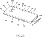
- FIG. 2B is a rear perspective view of an electronic device, according to an embodiment of the present disclosure.
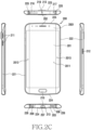
- FIG. 2C are various views of an electronic device, according to an embodiment of the present disclosure.
- a display 201 is installed on a front surface 2001 of an electronic device 200.
- a receiver 202 for receiving a voice of a caller is disposed at an upper area of the display 201.
- Components for performing various functions of the electronic device 200 are disposed around the receiver 202 on an upper area of the display 201.
- the components include at least one sensor module 204, a front camera device 205, and an indicator 206.
- the sensor module 204 may include, for example, an illuminance sensor (e.g., an optical sensor), a proximity sensor (e.g., an optical sensor), an infrared sensor, an ultrasonic sensor, etc.
- the front camera device 205 is for taking still or moving pictures.
- the indicator 206 is to inform the user of state information of the electronic device 200.
- the electronic device 200 includes a metal bezel 220 as a metal housing.
- the metal bezel 220 is disposed along the outer periphery of the electronic device 200 and may extend to at least a part of the rear surface of the electronic device 200, which is continuous to the outer periphery.
- the metal bezel 220 defines at least a part of the thickness of the electronic device 200 along the outer periphery of the electronic device 200, and may be formed in a closed loop shape. Without being limited thereto, however, the metal bezel 220 may be formed in a manner that contributes to at least a part of the thickness of the electronic device 200.
- the metal bezel 220 may only be disposed on a part of the outer periphery of the electronic device 200.
- a non-metal material may contribute to the remaining portion of the housing.
- the housing is formed in a manner of insert-molding the non-metal member to the metal bezel 220.
- the metal bezel 220 may include one or more cut-off portions 225 and 226 so that a unit bezel portion between the cut-off portions 225 and 226 may be utilized as an antenna radiator.
- An upper bezel portion 223 is a unit bezel portion bounded by one pair of cut-off portions 225 that are formed at a certain interval.
- a lower bezel portion 224 is a unit bezel portion bounded by one pair of cut-off portions 226 that are formed at a certain interval.
- the cut-off portions 225 and 226 may be formed when the non-metal member is insert-molded to the metal member.
- the metal bezel 220 includes a left bezel portion 221, a right bezel portion 222, the upper bezel portion 223, and the lower bezel portion 224, as viewed from the front side of the electronic device 200.
- Various components are disposed on the lower bezel portion 224 of the electronic device 200, such as a microphone device 203, an interface connector port 207, a speaker 208, and an ear jack hole 209.
- the microphone device 203 is for transmitting a voice of a user of the electronic device 200 to a caller.
- the interface connector port 207 is disposed adjacent to the microphone device 203 on one side.
- the interface connector port 207 performs a data transmission/reception function with respect to an external device and is used for charging the electronic device 200 by receiving an external power applied thereto.
- the speaker device 208 is disposed adjacent to the microphone device on 203 on the other side.
- the ear jack hole 209 is disposed adjacent to the interface connector port 207.
- the microphone device 203, the speaker device 208, the interface connector port 207, and the ear jack hole 209 are all disposed within the area of the unit bezel portion that is formed between one pair of cut-of portions 226 disposed in the lower bezel portion 224. Without being limited thereto, however, at least one of the above-described electronic components may be disposed in the area that includes the cut-off portion 226, or may be disposed outside the unit bezel portion.
- Various electronic components may also be disposed on the upper bezel portion 223 of the electronic device 200, such as a socket device 216, an auxiliary microphone device 217, and an infrared sensor module 218.
- the socket device 216 is for insertion of a card-type external device.
- the socket device 216 may accommodate at least one of an inherent identification (ID) card for the electronic device 200 (e.g., a subscriber identity module (SIM) card or a user identity module (UIM)), and a memory card for extending a storage space.
- ID inherent identification
- SIM subscriber identity module
- UIM user identity module
- the infrared sensor module 218 is disposed adjacent to the socket device 216 and the auxiliary microphone device 217 is disposed adjacent to the infrared sensor module 218.
- the socket device 216, the infrared sensor module 218, and the auxiliary microphone device 217 are disposed within the area of the unit bezel portion formed between one pair of cut-off portions 225 that are disposed in the upper bezel portion 223. Without being limited thereto, however, at least one of the above-mentioned electronic components may be disposed in the area that includes of the cut-off portion 225, or may disposed outside the cut-off portion.
- One or more first side key buttons 211 are disposed on the left bezel portion 221 of the metal bezel 220.
- the first side key buttons 211 partially protrude and are configured to perform a volume up/down function, a scroll function, etc.
- At least one second side key button 212 is disposed on the right bezel portion 222 of the metal bezel 220.
- the second side key button 212 is configured to perform a power ON/OFF function, a wake-up/sleep function, etc.
- At least one key button 210 is disposed in a lower area of the display 201.
- a fingerprint recognition sensor device may be disposed on the top surface of the key button 210.
- the key button 210 may be configured to perform a first function, such as a home screen return function, a wake-up/sleep function, etc., by physically pressing the key button 210, and to perform a second function, such as a fingerprint recognition function, by swiping the top surface of the key button 210.
- Touch pads may be disposed on the left and right of the key button 210 so as to perform a touch function.
- a rear camera device 213 is disposed on the rear surface 2002 of the electronic device 200, and one or more electronic components 214 is disposed adjacent to the rear camera device 213.
- the electronic components 214 may include at least one of an illuminance sensor (e.g., an optical sensor), a proximity sensor (e.g., an optical sensor), an infrared sensor, an ultrasonic sensor, a heartrate sensor, a flash device, etc.
- the front surface 2001 in which the display 201 is provided, includes a planar portion 2011, and a left bent portion 2012 and a right bent portion 2013 which are formed on the left and right of the planar portion 2011, respectively.
- the front surface 2001 of the electronic device 200 includes the display area 201 and other areas (e.g., a black matrix (BM) area) by using a single window.
- the left and right bent portions 2012 and 2013 are formed to extend in an x-axis direction of the electronic device 200 from the planar portion 2011, as shown in FIG. 2A .
- Each of the left and right bent portions 2012 and 2013 may be configured as a part of the side surfaces of the electronic device 200.
- the left and right bent portions 2012 and 2013 may be configured as the side surfaces of the electronic device 200 together with the left and right bezel portions 221 and 222 of the metal bezel 220, respectively.
- the front surface 2001 in which the display 201 is provided, may include only one of the left and right bent portions 2012 and 2013. That is, the front surface 2001 may be configured to include only the left bent portion 2012 along the planar portion 2011, or to include only the right bent portion 2013 along the planar portion 2011.
- the front surface 2001 may include a flexible display module that is applied to at least a portion of the window that includes the bent portions 2012 and 2013 on the left and right thereof, and the lower side of the window.
- the area including the flexible display module may be configured as the display 201.
- the window may be formed in a manner in which the top and rear surfaces thereof are simultaneously bent (hereinafter, a "three-dimensional (3D) type"). Without being limited thereto, the window may be formed in a manner in which the left and right portions of the top surface are formed in a curved shape and the rear surface is formed in a planar shape (hereinafter, "two-and-a-half dimensional (2.5D) type").
- the window may be formed of a transparent glass material (e.g., a sapphire glass) or a transparent synthetic resin material.
- the electronic device 200 may control the display module so as to selectively display information. Further, the electronic device 200 may control the display module so as to configure a screen only on the planar portion 2011, to configure a screen by any one of the left and right bent portions 2012 and 2013 together with the planar portion 2011 or to configure a screen by at least one of the left and right bent portions 2012 and 2013, excluding the planar portion 2011.
- the rear surface 2002 of the electronic device 200 may also be entirely formed by one window 215.
- the rear surface 2002 includes a planar portion 2151 that is substantially formed in a central portion to be the center, and a left bent portion 2152 and a right bent portion 2153, which are formed on the left and right of the planar portion 2151, respectively.
- the window 215 is configured in the 2.5D type in which the left and right bent portions 2152 and 2153 of the outer surface are formed in a curved shape and the rear surface is formed as a planar surface. Without being limited thereto, however, the window 215 may be formed in the 3D type, similar to the window disposed on the front surface 2001.
- Each of the left and right bent portions 2152 and 2153 may be configured as a part of the side surfaces of the electronic device 200.
- the left and right bent portion 2152 and 2153 may be configured as the side surfaces of the electronic device 200 together with the left and right bezel portions 221, 222 of the metal bezel 220.
- the rear surface 2002 may include only at least one of the left and right bent portions 2152 and 2153.
- the rear surface 2002 may be configured to include only the left bent portion 2152 along the planar portion 2151, or to include only the right bent portion 2153 along the planar portion 2151.
- the upper side left and right corner portions and the lower side left and right corner portions of the front surface 2001 may be formed to be simultaneously inclined in the x-axis direction, the y-axis direction, and the z-axis direction while the window is bent, as shown in FIGs. 2A and 2C .
- the upper side left and right corner portions and the lower side left and right corner portions of the metal bezel 220 may be formed such that the heights thereof gradually decrease towards their respective side surfaces.
- metal bezel 220 which is configured as a part of the housing of the electronic device 200, has been illustrated and described above, various embodiments of the present disclosure are not limited thereto.
- various metal members disposed on the electronic device 200 may be used for various embodiments of the present disclosure.
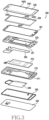
- FIG. 3 is an exploded perspective view of an electronic device in a disassembled state, according to an embodiment of the present disclosure.
- an electronic device 300 is provided.
- the electronic device 300 may be the same as the above-described electronic device 200.
- the electronic device 300 includes a printed circuit board (PCB) 360, a bracket 320, a display module 330, and a front window 340, which are disposed in a manner of being sequentially staked on the upper side of the housing 310.
- the electronic device includes a wireless power transmission/reception member 380 and a rear window 350, which are disposed in a manner of being sequentially staked on the lower side of the housing 310.
- a battery pack 370 is accommodated in an accommodation space 311, which is formed in the housing 310, and is disposed to avoid the PCB 360.
- the battery pack 370 and the PCB 360 are disposed in parallel not to overlap with each other.
- the display module 330 is fixed to the bracket 320, and the front window 340 is fixed by being attached to the bracket 320 by a first adhesive member 391.
- the rear window 350 is fixed by being attached to the housing 310 by a second adhesive member 392.
- the front window 340 includes a planar portion 3401, a left bent portion 3402, and a right bent portion 3403, which are bent in opposite directions from the planar portion 3401.
- the front window 340 is positioned on the electronic device 300 so as to form the front surface, and is formed of a transparent material so as to display a screen presented by the display module 330 and to provide an input/output window for various sensors.
- a touch panel may be further disposed on the rear surface of the front window 340 and may receive a touch input signal from the outside.
- the display module 330 may also be formed in a shape corresponding to that of the front window 340 (a shape having a curvature corresponding to that of the front window 340).
- the display module 330 includes a planar portion 3301, and left and right bent portions 3302 and 3303 on the left and right of the planar portion 3301.
- a flexible display module may be used as the display module 330.
- a window in a type where the rear surface of the front window 340 is formed in a planar shape hereinafter, 2D type or 2.5 D type
- an ordinary LCD or an on-cell touch screen panel (TSP) active matrix OLED (AMOLED) (OCTA) may be applied.
- the first adhesive member 391 is a component for fixing the front window 340 to a bracket 320 that is disposed within the electronic device 300, and may be a kind of tape, such as a double-sided tape, or a liquid adhesive layer, such as a bond.
- a general polyethylene terephthalate (PET), or a functional base may be applied as the internal base of the adhesive member 391.
- PET polyethylene terephthalate
- a base formed of a foam type or shock-resistive fabric material so as to reinforce the shock resistance, it is possible to prevent the front window 340 from being destroyed by external impact.
- the bracket 320 is a component used for reinforcing the entire rigidity of the electronic device 300.
- the bracket 320 may be formed of at least one metal selected from aluminum (Al), magnesium (Mg), and STS.
- the bracket 320 may be formed of a highly rigid plastic, in which glass fibers are contained, or may be formed of a combination of a metal and a plastic. When a metal member and a non-metal member are used in combination, the bracket 320 is formed by insert-molding the non-metal member to the metal member. The bracket 320 is placed on the rear surface of the display module 330.
- the bracket 320 has a shape (curvature) that is similar to the shape of the rear surface of the display module 330 and supports the display module 330. Between the bracket 320 and the display module 330, an elastic member, such as a sponge or a rubber, and the first adhesive member 391, such as a liquid adhesive, a double-sided tape, or a kind of sheet, such as a single-sided tape, may be additionally disposed so as to protect the display module 330.
- a section of the bracket 320 further includes a slot-sinking or hole area 321 for securing a component mounting space or a marginal space based on a change of a component during use, such as the swelling of the battery pack 370.
- a sheet-type meal or composite material may be added to the corresponding hole area 321 so as to reinforce the internal rigidity, or an auxiliary device for improving a thermal characteristic, an antenna characteristic, etc., may be further provided in the hole area 321.
- the bracket 320 is fastened to the housing 310 (e.g., the rear case) so as to form a space therein, and at least one electronic component may be disposed in such a space.
- the at least one electronic component may include the PCB 360. Without being limited thereto, however, the at least one electronic component may include an antenna device, a sound device, a power supply device, a sensor device, etc., in addition to the PCB 360.
- the battery pack 370 supplies power to the electronic device 300.
- One surface of the battery pack 370 is positioned close to the display module 330 and the other surface is positioned close to the rear window 350, so that if the battery pack 370 swells during charge, adjacent components may be deformed or destroyed.
- a the hole area 321, as described above, is provided between the battery pack 370 and the adjacent components (e.g., the display module 330 and the rear window 350) so as to protect the adjacent components.
- the battery pack 370 may be integrated with the electronic device 300. Without being limited thereto, however, when the rear window 350 is implemented to be attachable to/detachable from the electronic device 300, the battery pack 370 may be implemented to be attachable/detachable.
- the housing 310 forms the exterior of the electronic device 300 (e.g., side surfaces including a metal bezel), and is coupled to the bracket 320 so as to form an internal space.
- the front window 340 is disposed on the front surface of the housing 310
- the rear window 350 is disposed on the rear surface of the housing 310.
- the rear surface of the housing 310 may be variously implemented by molding a synthetic resin, or by using a metal, a composite of a metal and a synthetic resin, etc.
- An inter-structure gap formed by the housing 310 and the rear window 350 prevents the destruction of the rear window 350 from a secondary impact by an internal structure when an external impact occurs, such as a drop of the electronic device 300.
- the wireless power transmission/reception member 380 is disposed on the rear surface of the housing 310.
- the wireless power transmission/reception member 380 has a thin film form and is disposed by being attached to one surface of an internally mounted component or an area of the inner surface of the housing 310, in particular to an area that is generally close to the rear window 350.
- the wireless power transmission/reception member 380 includes a structure that forms a contact with the PCB 360 within the housing 310.
- the wireless power transmission/reception member 380 may be embedded or attached as a component of the battery pack 370, etc., or a part of the housing 310, and may be provided in the form of being attached to both of a component and the housing 310.
- the second adhesive member 392 is a component that fixes the rear window 350 to the housing 310 and may be applied in a form similar to that of the first adhesive member 391 described above.
- the rear window 350 may be applied in a form similar to that of the front window 340.
- the front surface (the surface exposed to the outside) of the rear window 350 is formed in a curvature that is more inclined in the direction of the left and right ends.
- the rear surface of the rear window 350 is formed in a planar surface to be attached to the hosing 310 by the second adhesive member 392.
- FIG. 4A is a cross-sectional view of an electronic device in an assembled state, according to an embodiment of the present disclosure.
- FIG. 4B is a cross-sectional view of a principal portion an electronic device in an assembled state, according to an embodiment of the present disclosure.
- a cross-sectional view of the electronic device 300 is provided.
- the bracket 320 is fixed to the housing 310 of the electronic device 300.
- the housing 310 may be formed by injection-molding a non-metal member (e.g., polycarbonate (PC)) 313 to the metal bezel 312.
- the display module 330 is fixed to the front surface of the bracket 320, and the front window 340 is disposed on the display module 330.
- the front window 340 is fixed by being attached to the bracket 320 by the first adhesive member 391 adjacent to an end of the housing 310 to correspond to the shape thereof on the end of the housing 310.
- the front window 340 is fixed by being attached to the bracket 320 by the first adhesive member 391 while being supported by the end of the housing 310.
- the front window 340 has a uniform thickness and is formed in a shape having a certain curvature. All of the planar portion 3401 and the left and right bent portions 3402 and 3403 of the front window 340 are formed to have a certain thickness.
- the rear window 350 is also fixed to the housing 310 by the second adhesive member 392.
- the rear window 350 is formed to have a thickness that is reduced towards the left and right edges (a shape which is formed in the 2.5D type).
- the PCB 360 is accommodated, and the battery pack 370 is disposed in parallel with the PCB 360 to avoid the PCB 360.
- FIG. 5 illustrates a metal member and a non-metal member which are applied to a housing of an electronic device, according to an embodiment of the present disclosure.
- the housing 310 includes a metal member 3310 and a non-metal member 3320 that is insert-molded to the metal member 3310.
- the metal member 3310 includes the metal bezel 220, as shown in FIGs. 2A and 2B .
- the metal member 3310 includes a metal structure that extends to at least a part of the front surface and/or the rear surface of the electronic device 300 from the metal bezel 220.
- the metal member 3310 includes a metal filler 3311 that is independently formed in a space separate from the metal bezel 220.
- the non-metal member 3320 includes an upper member 3321 and a lower member 3322.
- the non-metal member 3320 includes a plurality of insulation members 3323 that are applied to the metal member 3310.
- the insulation members 3323 contribute to the insulation between the metal member 3310 and the PCB 360 when fixing the housing 310 and the bracket 320, or fixing the PCB 360 through screws.
- FIGs. 6A and 6B are views illustrating a process of manufacturing a housing of an electronic device, according to an embodiment of the present disclosure.
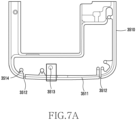
- FIGs. 7A and 7B are views of a metal member and a non-metal member after a final manufacturing process, according to an embodiment of the present disclosure.
- a primary processing is performed by extruding a plate-type metal base material, and a non-metal member 3320 is insert-molded to the primarily processed metal base material, i.e. the metal member 3310. After the non-metal member 3320 is insert-molded to the metal member 3310, a final processing is performed.
- a primarily processed base material 3420 is obtained by extruding a plate-type metal base material 3410.
- the primarily processed base material 3420 includes a protruding portion 3423 and a plurality of recessed portions 3421 and 3422 that are formed to be relatively lower that the protruding portion 3423.
- a non-metal member 3430 is insert-molded to at least a part of the plurality of recessed portions 3421 and 3422 and the protruding portion 3423 of the primarily processed metal base material 3420.
- the protruding portion 3423 serves as a metal filler 3423 that is disposed independently from the primarily processed base material 3420.
- FIGs. 7A and 7B are views of a metal and a non-metal member after a final manufacturing process, according to an embodiment of the present disclosure.
- a metal member 3510 is illustrated after the insert-molding and the final processing of a non-metal member 3520 have been completed.
- the non-metal member 3520 e.g., PC
- the metal bezel 3510 is disposed to surround the outer periphery of the electronic device 300, and one pair of cut-off portions 3512 are formed at a certain interval at the lower side of the metal bezel 3510.
- the unit bezel portion 3511 is formed independently from the metal bezel 3510.
- the unit bezel portion 3511 may serve as an antenna member.
- a part of the unit bezel portion 3511 forms a contact portion 3514 that is drawn out to extend to the inside of the electronic device 300.
- a metal filler 3513 is operated as a metal island to be used as an electric connection member in the vertical direction between a DPA, which is disposed in the housing 310, and a PCB 360 that is disposed inside the electronic device 300.
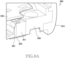
- FIGs. 8A and 8B are views of a housing in a state in which a metal filler is used as an electric connection member of an antenna device, according to an embodiment of the present disclosure.
- a metal filler 3611 is disposed to be isolated by a non-metal member 3620 that is insert-molded to a metal member 3610 that is used as the metal bezel 3510.
- the metal member 3610 and the non-metal member 3620 contribute to at least a part of the housing 3600 of the electronic device 300. At least a part of the metal filler 3611 may be exposed to an outer surface of the non-metal member 3620. Alternatively, at least a part of the metal filler 3611 may be exposed to an inner surface of the non-metal member 3620.
- An antenna radiator 3640 is disposed on and attached to the outer surface of the housing 3600. Without being limited thereto, however, the antenna radiator 3540 may be formed on the outer surface of the housing 3600 by an LDS or DPA method. The antenna radiator 3640 is physically in contact with the metal filler 3611 exposed to the outer surface of the housing 3600.
- a PCB 3630 is disposed within the electronic device 300, and an electric connection member 3631 is interposed between the PCB 3630 and the metal filler 3611.
- Various members such as a C-clip, a thin wire cable, and a flexible printed circuit, may be used as the electric connection member 3631.
- the antenna radiator (DPA) 3640 attached to the outer surface of the housing 3600, is electrically connected to the PCB 3630 through the metal filler 3611 and the electric connection member 3631, so that the antenna radiator 3640 may be used as an additional antenna radiator of the electronic device or an independent antenna radiator.
- FIG. 9 is a view of a principal portion of a housing in a state where a non-metal member is insert-molded to a metal member, according to an embodiment of the present disclosure.
- the non-metal member 3270 is formed on a metal member 3710 by insert-molding. Because the metal member 3710 and the non-metal member 3720 are bonded to each other through bonding between dissimilar materials, the metal member 3710 and the non-metal member 3720 preferably have a separate and additional binding structure.
- the metal member 3710 includes a metal bezel 3714 and a unit bezel 3711 that is separated from the metal bezel 3714 by cut-off portions 3715.
- the metal bezel 3714 includes a flange 3712 that is formed to extend inwardly, and at least one molding opening 3713 is formed in the flange 3712.
- the non-metal member 3720 when the non-metal member 3720 is insert-molded to the metal member 3710, the non-metal member 3720 may be insert-molded to the molding opening 3713 of the metal member 3710 to serve as a non-metal filler 3721, which supports the binding force between the metal member 3710 and the non-metal member 3720 which are dissimilar materials.
- FIGS. 10A to 10C are views of various configurations of a housing in a state in which a non-metal member is insert-molded to a metal member, according to an embodiment of the present disclosure.
- FIGs. 10A to 10C a bonding structure for improving the adhesive force between dissimilar materials (a metal material and a non-metal material) by the structure of the metal member itself is illustrated.
- a recess 3811 is formed on a metal member 3810, and a non-metal member 3820 is insert-molded to the recess 3811 to be formed as a protrusion 3821 so as to support the bonding force between dissimilar materials.
- the metal member 3810 and the non-metal member 3820 are insert-molded, and a metal filler 3812, which is disposed to be spaced apart from the metal member 3810, causes a plurality of protrusions 3813 along an outer peripheral surface thereof to be molded as non-metal members. Accordingly, it is possible to prevent in advance the metal filler 3812 from being separated or moved in the vertical direction by a pressing force of an electric connection member 3831, which is installed on the PCB 3830 and has a certain elasticity.
- the metal member 3810 and the non-metal member 3820 are insert-molded, and a metal filler 3814, which is disposed to be spaced apart from the metal member 3810, is also processed by performing a process, such as sanding or chemical etching, on an outer surface of the metal filler 3814 during the extrusion process.
- a process such as sanding or chemical etching
- the surface frictional force is increased so that the bonding force of the metal filler 3814 with the non-metal 3820 is increased. Accordingly, it is possible to prevent in advance the metal filler 3821 from being separated or moved in the vertical direction by the pressing force of the electric connection member 3831, which is installed on the PCB 3830 and has a certain elasticity.
- FIGs. 11A and 11B are views of a housing in a state where a non-metal member is used as an insulation member in a metal member, according to an embodiment of the present disclosure.
- a housing 3900 is formed by insert-molding a non-metal member 3920 to a metal member 3910.
- a non-metal member 3920 On the metal member 3910, one or more insulation members 3921 by the non-metal member 3920 are disposed.
- Each insulation member 3921 accommodates a screw 3930, and is configured to prevent in advance an electric shock accident that is caused by electric power applied to the metal member 3910 through a structure 3940 (e.g., a PCB) within the electronic device 300.
- the insulation member 3921 which is insert-molded in the metal member 3910, is formed in a hollow shape to have a depth that is at least the same as the entire height of the metal member 3910.
- the screw 3930 inserted into the insulation member 3921 is fastened to the structure 3940 of the electronic device.
- the structure 3940 may be a PCB, a bracket, etc. Accordingly, the metal member 3910 is maintained in the state in which it is completely insulated from the structure 3940 within the electronic device 300 by the insulation member 3921, so that an electric shock accident can be prevented in advance.
- a housing is capable of directly connecting a metal member and an antenna radiator to each other so that an additional mounting space on a PCB may not be required, and various connection conditions are enabled depending on a portion of an external exposed face of the metal member without requiring a separate component so that an error and a deviation caused by an additional process may be excluded.
Description
- The present disclosure relates generally to an electronic device, and more particularly to manufacturing the housing, and an electronic device including the housing.
- As the functional differences between electronic devices of different manufacturers have recently been greatly reduced, manufacturers have gradually begun to develop slimmer electric devices in order to satisfy consumers' purchasing needs. Further, manufacturers are developing electronic devices with increased rigidity and strengthened design features in mind. As a result, various exterior structures of the electronic devices are at least partially implemented by using a metal material to provide the exterior surfaces with luxuriousness and elegance.
- Further, efforts are being made to solve the problems of weakened rigidity, grounding (e.g., electric shock), deterioration of an antenna radiation performance that are caused by using the metal material on the exterior structures, etc.
- An exterior structure of an electronic device, such as a housing, may be manufactured using different materials. For example, the housing may be formed by insert molding a non-metal member to a metal member and the non-metal member may be made of a synthetic resin material.
- An electronic device that includes a housing having a metal member in at least a portion thereof, may require an electric connection structure between a Printed Circuit Board (PCB) arranged within the internal space of the electronic device and an electronic component generally arranged on the outer face of the electronic device (e.g., an antenna radiator). For example, in the case of the antenna radiator, a conventional antenna carrier or a Flexible PCB (FPCB) electric connection structure includes a flexible antenna radiator so that the antenna radiator can be vertically connected to a pattern face. Furthermore, the conventional antenna carrier or FPCB connection structure is flexible so that a pattern shift is enabled from a radiation face of the antenna radiator to a PCB contact face. However, a problem may occur in securing a space that is essentially needed for the pattern shift.
- In the case of a Direct Print Antenna (DPA) or an Laser Direct Structuring (LDS) antenna, which is directly printed on the housing, the antenna is not able to be vertically connected to a radiation pattern so that an electric connection can be achieved using a separate metallic press-fitting pin. However, a housing structure using such a press-fitting pin requires an additional process of applying an additional component, and may cause degradation of the radiation performance of an antenna due to a deviation or an error that is caused as a result of assembly. Additionally, such housing structures generally face the following problems: an increase in manufacturing costs due to the added component; the press-fitting pins may not be able to be applied to a complicated structural portion of the housing structure, such as a curved face; and a peripheral portion, around the housing structure, may be scratched or deformed in the process of press-fitting.
- In addition, a conventional screw fastening structure may present electric shock problems. For example, with a conventional screw an internal current may be transferred to an external metal housing through the screw, thereby being exposed to electric shock. In order to prevent this, a capacitor may be arranged around the screw as an electric safety device, which may also increases unit price, and a separate mounting space is needed by adopting an additional component. Known from the art is for example an electronic device as disclosed in
US2014228080A1 , which is provided including a plurality of electronic parts; one or more housing components forming a space for receiving the plurality of electronic parts; and a cover detachable from the one or more housing components, the cover including a first member having a plurality of metal elements suspended in a non-metal base and a second member coupled to the first member. Furthermore, known from the art is for example a mobile terminal as disclosed inUS2014085836A1 provided with a case having an inner space where electronic components are mounted, a display arranged in the inner space of the case, the display being exposed at a front surface of the case, an audio output module arranged in the inner space of the case to output sound, a circuit board arranged in the inner space of the case, the circuit board having a circuit pattern to transmit an electric signal, a bracket coupled to a back surface of the display, the bracket including a metallic plate and an injection mold configured to partially cover the metallic plate and an electric current carrying structure configured to electrically connect the metal plate to at least one of the display, the audio output module and the circuit board. Furthermore, reference is made to prior art documentsUS2013085836A1 andUS2003019662A1 . - The present disclosure has been made to address at least the above-described problems and disadvantages, and to provide at least the advantages described below.
- The invention is as set out in claim 1, preferred forms being set out in the dependent claims 2 to 13.
- The above and other aspects, features, and advantages of the present disclosure will be more apparent from the following detailed description taken in conjunction with the accompanying drawings, in which:
-
FIG. 1 is a block diagram of a configuration of a network environment including an electronic device, according to an embodiment of the present disclosure; -
FIG. 2A is a front perspective view of an electronic device, according to an embodiment of the present disclosure; -
FIG. 2B is a rear perspective view of an electronic device according to an embodiment of the present disclosure; -
FIG. 2C are various views of an electronic device, according to an embodiment of the present disclosure; -
FIG. 3 is an exploded perspective view of an electronic device in a disassembled state, according to an embodiment of the present disclosure; -
FIG. 4A is a cross-sectional view of an electronic device in an assembled state, according to an embodiment of the present disclosure; -
FIG. 4B is a cross-sectional view of a principal portion of an electronic device in an assembled state, according to an embodiment of the present disclosure; -
FIG. 5 illustrates views of a metal member and a non-metal member, which are applied to a housing of an electronic device, according to an embodiment of the present disclosure; -
FIGs. 6A and6B are views illustrating a process of manufacturing a housing of an electronic device, according to an embodiment of the present disclosure; -
FIGs. 7A and7B are views of a metal member and a non-metal member after a final manufacturing process, according to an embodiment of the present disclosure; -
FIGs. 8A and8B are views of a housing a state in which a metal filler is used as an electric connection member of an antenna device, according to an embodiment of the present disclosure; -
FIG. 9 is a view of a principal portion of a housing in a state where a non-metal member is insert-molded to a metal member, according to an embodiment of the present disclosure; -
FIGs. 10A to 10C are views of various configurations of a housing in a state in which a non-metal member is insert-molded to a metal member, according to an embodiment of the present disclosure; and -
FIGs. 11A and11B are views of a housing in a state where a non-metal member is used as an insulation member in a metal member, according to an embodiment of the present disclosure. - The following description with reference to the accompanying drawings is provided to assist in a comprehensive understanding of various embodiments of the present disclosure as defined by the claims.
- Descriptions of well-known functions and constructions may be omitted for clarity and conciseness. In describing the drawings, similar reference numerals designate similar constituent elements.
- The terms and words used in the following description and claims are not limited to their dictionary meanings, but are merely used to enable a clear and consistent understanding of the present disclosure. Accordingly, it should be apparent to those skilled in the art that the following description of various embodiments of the present disclosure is provided for illustration purposes only and not for the purpose of limiting the present disclosure as defined by the appended claims
- It is to be understood that the singular forms "a," "an," and "the" include plural referents unless the context clearly dictates otherwise. Thus, for example, reference to "a component surface" includes reference to one or more of such surfaces.
- By the term "substantially" it is meant that the recited characteristic, parameter, or value need not be achieved exactly, but that deviations or variations, including for example, tolerances, measurement error, measurement accuracy limitations, and other factors known to those of skill in the art, may occur in amounts that do not preclude the effect the characteristic was intended to provide.
- The terms "have", "may have", "include", and "may include" as used herein indicate the presence of disclosed corresponding functions, operations, elements, etc., and do not limit additional one or more functions, operations, elements, etc. In addition, the terms "include" and "have" indicate the presence of features, numbers, operations, elements, parts, or a combination thereof described in the specifications, and do not preclude the presence or addition of one or more other features, numbers, operations, elements, parts, or a combination thereof.
- The terms "A or B", "at least one of A or/and B" and "one or more of A or/and B" as used herein include any and all combinations of words enumerated with it. For example, "A or B", "at least one of A and B" or "at least one of A or B" describes (1) including A, (2) including B, or (3) including both A and B.
- Although terms, such as "first" and "second" as used herein may modify various elements, these terms do not limit the corresponding elements. For example, these terms do not limit an order and/or importance of the corresponding elements. These terms may be used for the purpose of distinguishing one element from another element. For example, a first user device and a second user device both indicate user devices and may indicate different user devices. For example, a first element may be referred to as a second element without departing from the scope of the present disclosure, and similarly, a second element may be referred to as a first element.
- When an element (e.g., a first element) is "connected to" or (operatively or communicatively) "coupled with/to" another element (e.g., a second element), the first element may be directly connected or coupled to the second element, and there may be an intervening element (e.g., a third element) between the first element and the second element. To the contrary, when an element (e.g., the first element) is "directly connected" or "directly coupled" to another element (e.g., the second element), there is no intervening element (e.g., the third element) between the first element and the second element.
- The expressions "configured to" and "set to" as used herein may be replaced with "suitable for", "having the capacity to", "designed to", " adapted to", "made to", or "capable of" according to the situation. The term "configured/set to" does not necessarily indicate "specifically designed to" in a hardware level. Instead, the expression "apparatus configured to..." may indicate that the apparatus is "capable of..." along with other devices or parts in a certain situation. For example, "a processor configured/set to perform A, B, and C" may be a dedicated processor, e.g., an embedded processor, for performing a corresponding operation, or a generic-purpose processor, e.g., a central processing unit (CPU) or an application processor (AP), capable of performing a corresponding operation by executing one or more software programs stored in a memory device.
- The terms as used herein merely describe certain embodiments of the present disclosure and are not intended to limit the present disclosure. Further, all the terms used herein, including technical and scientific terms, should be interpreted to have the same meanings as commonly understood by those skilled in the art to which the present disclosure pertains, and should not be interpreted to have ideal or excessively formal meanings, unless explicitly defined herein.
- A module or programming module, according to various embodiments of the present disclosure, may further include at least one or more of the aforementioned constituent elements, may omit some of them, or may further include additional constituent elements. Operations performed by a module, programming module, or other constituent elements may be executed in a sequential, parallel, repetitive, or heuristic manner. In addition, some of the operations may be executed in a different order or may be omitted, or other operations may be added.
- An electronic device, according to various embodiments of the present disclosure, may include at least one of a smart phone, a tablet personal computer (PC), a mobile phone, a video phone, an e-book reader, a desktop PC, a laptop PC, a netbook computer, a workstation, a server, a personal digital assistant (PDA), a portable multimedia player (PMP), a moving picture experts group phase 1 or phase 2 (MPEG-1 or MPEG-2) audio layer 3 (MP3) player, a mobile medical device, a camera, or a wearable device (e.g., a head-mounted-device (HMD), electronic glasses, electronic clothing, an electronic bracelet, an electronic necklace, an electronic appcessory, an electronic tattoo, a smart mirror, a smart watch, etc.).
- An electronic device may also be a smart home appliance. For example, smart home appliances may include at least one of a television (TV), a digital versatile disc (DVD) player, an audio component, a refrigerator, an air conditioner, a vacuum cleaner, an oven, a microwave oven, a washing machine, an air cleaner, a set-top box, a home automation control panel, a security control panel, a TV box (e.g., Samsung HomeSync®, Apple TV®, or Google TV), a game console (e.g., Xbox® PlayStation®), an electronic dictionary, an electronic key, a camcorder, an electronic frame, etc.
- An electronic device may also include at least one of a medical equipment (e.g., a mobile medical device (e.g., a blood glucose monitoring device, a heart rate monitor, a blood pressure monitoring device, a temperature meter, etc.), a magnetic resonance angiography (MRA) machine, a magnetic resonance imaging (MRI) machine, a computed tomography (CT) scanner, an ultrasound machine, etc.), a navigation device, a global positioning system (GPS) receiver, an event data recorder (EDR), a flight data recorder (FDR), an in-vehicle infotainment device, electronic equipment for a ship (e.g., ship navigation equipment and/or a gyrocompass), avionics equipment, security equipment, a head unit for a vehicle, an industrial or home robot, an automatic teller machine (ATM), a point of sale (POS) device, or an Internet of Things (IoT) device (e.g., a light bulb, various sensors, an electronic meter, a gas meter, a sprinkler, a fire alarm, a thermostat, a streetlamp, a toaster, sporting equipment, a hot-water tank, a heater, a boiler, etc.)
- An electronic device may also include at least one of a piece of furniture or a building/structure, an electronic board, an electronic signature receiving device, a projector, and various measuring instruments (e.g., a water meter, an electricity meter, a gas meter, a wave meter, etc.).
- An electronic device may also include a combination of one or more of the above-mentioned devices.
- Further, it will be apparent to those skilled in the art that an electronic device is not limited to the above-mentioned examples.
- Herein, the term "user" may indicate a person who uses an electronic device or a device (e.g., an artificial intelligence electronic device) that uses the electronic device.
- An electronic device of a single radio environment can provide long-term evolution (LTE) service using circuit switched fall back (CSFB) which determines whether paging information of a circuit switched (CS) service network is received over an LTE network. When receiving a paging signal of the CS service network over the LTE network, the electronic device connects (or accesses) the CS service network (e.g., a 2nd generation (2G)/3rd generation (3G) network) and provides a voice call service. For example, the 2G network can include one or more of a global system for mobile communications (GSM) network and a code division multiple access (CDMA) network. The 3G network can include one or more of a wideband-CDMA (WCDMA) network, a time division-synchronous CDMA (TD-SCDMA) network, and an evolution-data optimized (EV-DO) network.
- Alternatively, the electronic device of the single radio environment can provide LTE service using single radio LTE (SRLTE) which determines whether the paging information is received by periodically switching every radio resource (e.g., receive antennas) to the CS service network (e.g., the 2G/3G network). Upon receiving the paging signal of the CS service network, the electronic device provides the voice call service by connecting the CS service network (e.g., the 2G/3G network).
- Alternatively, the electronic device of the single radio environment can provide LTE service using single radio dual system (SRDS) which determines whether the paging information is received by periodically switching some of radio resources (e.g., receive antennas) to the CS service network (e.g., the 2G/3G network). Upon receiving the paging signal of the CS service network, the electronic device provides the voice call service by connecting the CS service network (e.g., the 2G/3G network).
-
FIG. 1 is a block diagram of a configuration of a network environment including an electronic device, according to an embodiment of the present disclosure. - Referring to
FIG. 1 , anelectronic device 101 in anetwork environment 100 is provided. Theelectronic device 101 includes abus 110, aprocessor 120, amemory 130, an input/output interface 150, adisplay 160, and acommunication interface 170. Theelectronic device 101 can omit at least one of the components or further include another component. - The
bus 110 is a circuit for connecting the components of the electronic device 101 (e.g., theprocessor 120, thememory 130, the input/output interface 150, thedisplay 160, and the communication interface 170) and delivering communications (e.g., a control message) therebetween. - The
processor 120 includes one or more of a CPU, an AP, and a communication processor (CP). Theprocessor 120 processes an operation or data on control of and/or communication with another component of theelectronic device 101. - The
processor 120, which is connected to the LTE network, determines whether a call is connected over the CS service network using caller identification information (e.g., a caller phone number) of the CS service network (e.g., the 2G/3G network). For example, theprocessor 120 receives incoming call information (e.g., a CS notification message or a paging request message) of the CS service network over the LTE network (e.g., CSFB). Alternatively, theprocessor 120, being connected to the LTE network, receives incoming call information (e.g., a paging request message) over the CS service network (e.g., SRLTE). - When receiving the incoming call information (e.g., a CS notification message or a paging request message) of the CS service network over the LTE network, the
processor 120 obtains caller identification information from the incoming call information. Theprocessor 120 displays the caller identification information on itsdisplay 160. Theprocessor 120 determines whether to connect the call based on input information corresponding to the caller identification information displayed on thedisplay 160. For example, when detecting input information corresponding to an incoming call rejection, through the input/output interface 150, theprocessor 120 restricts the voice call connection and maintains the LTE network connection. For example, when detecting input information corresponding to an incoming call acceptance, through the input/output interface 150, theprocessor 120 connects the voice call by connecting to the CS service network. - When receiving the incoming call information (e.g., a CS notification message or a paging request message) of the CS service network over the LTE network, the
processor 120 obtains caller identification information from the incoming call information. Theprocessor 120 determines whether to connect the call by comparing the caller identification information with a reception control list. For example, when the caller identification information is included in a first reception control list (e.g., a blacklist), theprocessor 120 restricts the voice call connection and maintains the connection to the LTE network. When the caller identification information is not included in the first reception control list (e.g., the blacklist), theprocessor 120 connects the voice call by connecting to the CS service network. When the caller identification information is included in a second reception control list (e.g., a white list), theprocessor 120 connects the voice call by connecting to the CS service network. - When receiving the incoming call information (e.g., a paging request message) of the CS service network over the LTE network, the
processor 120 transmits an incoming call response message (e.g., a paging response message) to the CS service network. Theprocessor 120 suspends the LTE service and receives the caller identification information (e.g., a CS call (CC) setup message) from the CS service network. Theprocessor 120 determines whether to connect the call by comparing the caller identification information with the reception control list. For example, when the caller identification information is included in the first reception control list (e.g., the blacklist), theprocessor 120 restricts the voice call connection and resumes the LTE network connection. When the caller identification information is not included in the first reception control list (e.g., the blacklist), theprocessor 120 connects the voice call by connecting to the CS service network. When the caller identification information is included in the second reception control list (e.g., the white list), theprocessor 120 connects the voice call by connecting to the CS service network. - The
memory 130 includes volatile and/or nonvolatile memory. Thememory 130 stores commands or data (e.g., the reception control list) relating to at least one of the other components of theelectronic device 101. Thememory 130 may store software and/or aprogram 140. Theprogram 140 may include, for example, akernel 141,middleware 143, an application programming interface (API) 145,applications 147. At least some of thekernel 141, themiddleware 143, and theAPI 145 may be referred to as an operating system (OS). - The
kernel 141 controls or manages system resources (e.g., thebus 110, theprocessor 120, or the memory 130) used for performing an operation or function implemented by the other programs (e.g., themiddleware 143, theAPI 145, or the applications 147). Furthermore, thekernel 141 provides an interface through which themiddleware 143, theAPI 145, or theapplications 147 connects the individual elements of theelectronic device 101 to control or manage the system resources. - The
middleware 143 functions as an intermediary for allowing theAPI 145 or theapplications 147 to communicate with thekernel 141 to exchange data. - In addition, the
middleware 143 processes one or more task requests received from theapplications 147 according to priorities thereof. For example, themiddleware 143 assigns priorities for using the system resources (e.g., thebus 110, theprocessor 120, thememory 130, etc.) of theelectronic device 101, to at least one of theapplications 147. For example, themiddleware 143 may perform scheduling or load balancing on the one or more task requests by processing the one or more task requests according to the priorities assigned thereto. - The
API 145 is an interface through which theapplications 147 control functions provided from thekernel 141 or themiddleware 143, and may include at least one interface or function (e.g., an instruction) for file control, window control, image processing, text control, etc.. - The input/
output interface 150 functions as an interface that transfers instructions or data input from a user or another external device to the other element(s) of theelectronic device 101. Furthermore, the input/output interface 150 outputs the instructions or data received from the other element(s) of theelectronic device 101 to the user or an external electronic device, such as a first externalelectronic device 102, asecond externalelectronic device 104, or aserver 106. - The
display 160 may include a liquid crystal display (LCD), a light emitting diode (LED) display, an organic LED (OLED) display, a micro electro mechanical system (MEMS) display, an electronic paper display, etc. Thedisplay 160 displays various types of content (e.g., a text, images, videos, icons, symbols, etc.) for the user. Thedisplay 160 may include a touch screen and receive, for example, a touch, a gesture, proximity, a hovering input, etc., using an electronic pen or the user's body part. Thedisplay 160 may display a web page. - The
communication interface 170 establishes a communication between theelectronic device 101 and the first externalelectronic device 102, the second externalelectronic device 104, or theserver 106. For example, thecommunication interface 170 communicates with the first externalelectronic device 102 through a wireless communication or awired communication 164, and also communicates with the second externalelectronic device 104 or theserver 106 in connection to anetwork 162 through wireless communication or wired communication. - The wireless communication can conform to a cellular communication protocol including at least one of LTE, LTE-advanced (LTE-A), CDMA, WCDMA, universal mobile telecommunications system (UMTS), wireless broadband (WiBro), and GSM.
- The wired communication can include at least one of universal serial bus (USB), high definition multimedia interface (HDMI), recommended standard 232 (RS-232), and plain old telephone service (POTS).
- The
network 162 can include at least one of telecommunications networks, for example, a computer network (e.g., a local area network (LAN) or a wide area network (WAN)), the Internet, a telephone network, etc. - The
electronic device 101 provides the LTE service in the single radio environment by use of at least one module functionally or physically separated from theprocessor 120. - Each of the first external
electronic device 102 and the second externalelectronic device 104 may be a type of device that is the same as or different from theelectronic device 101. Theserver 106 may include a group of one or more servers. - All or some of the operations to be executed by the
electronic device 101 may be executed by another electronic device or a plurality of other electronic devices, such as the first externalelectronic device 102, the second externalelectronic device 104, or theserver 106. In the case where theelectronic device 101 should perform a certain function or service automatically or by request, theelectronic device 101 may request some functions that are associated therewith from the first externalelectronic device 102, the second externalelectronic device 104 or theserver 106 instead of or in addition to executing the function or service by itself. The first externalelectronic device 102, the second externalelectronic device 104, or theserver 106 may execute the requested functions or additional functions, and may transmit the results to theelectronic device 101. Theelectronic device 101 may provide the requested functions or services by processing the received results as they are or additionally. For this purpose, for example, a cloud computing technique, a distributed computing technique, or a client-server computing technique may be used. - Various embodiments of the present disclosure will be described with reference to a
display 160 that includes a bent or curved area and is applied to a housing of theelectronic device 101, in which a non-metal member and a metal member (e.g., a metal bezel) are formed through dual injection molding, but are not limited thereto. For example, thedisplay 160 may be applied to a housing, in which a metal member or a non-metal member is formed of a single material. -
FIG. 2A is a front perspective view of an electronic device, according to an embodiment of the present disclosure.FIG. 2B is a rear perspective view of an electronic device, according to an embodiment of the present disclosure.FIG. 2C are various views of an electronic device, according to an embodiment of the present disclosure. - Referring to
FIGs. 2A to 2C , adisplay 201 is installed on afront surface 2001 of anelectronic device 200. Areceiver 202 for receiving a voice of a caller is disposed at an upper area of thedisplay 201. Components for performing various functions of theelectronic device 200 are disposed around thereceiver 202 on an upper area of thedisplay 201. The components include at least onesensor module 204, afront camera device 205, and anindicator 206. Thesensor module 204 may include, for example, an illuminance sensor (e.g., an optical sensor), a proximity sensor (e.g., an optical sensor), an infrared sensor, an ultrasonic sensor, etc. Thefront camera device 205 is for taking still or moving pictures. Theindicator 206 is to inform the user of state information of theelectronic device 200. - The
electronic device 200 includes ametal bezel 220 as a metal housing. Themetal bezel 220 is disposed along the outer periphery of theelectronic device 200 and may extend to at least a part of the rear surface of theelectronic device 200, which is continuous to the outer periphery. Themetal bezel 220 defines at least a part of the thickness of theelectronic device 200 along the outer periphery of theelectronic device 200, and may be formed in a closed loop shape. Without being limited thereto, however, themetal bezel 220 may be formed in a manner that contributes to at least a part of the thickness of theelectronic device 200. Themetal bezel 220 may only be disposed on a part of the outer periphery of theelectronic device 200. When themetal bezel 220 contributes to a part of the housing of theelectronic device 200, a non-metal material may contribute to the remaining portion of the housing. In such a case, the housing is formed in a manner of insert-molding the non-metal member to themetal bezel 220. - The
metal bezel 220 may include one or more cut-offportions portions upper bezel portion 223 is a unit bezel portion bounded by one pair of cut-offportions 225 that are formed at a certain interval. Alower bezel portion 224 is a unit bezel portion bounded by one pair of cut-offportions 226 that are formed at a certain interval. The cut-offportions - The
metal bezel 220 includes aleft bezel portion 221, aright bezel portion 222, theupper bezel portion 223, and thelower bezel portion 224, as viewed from the front side of theelectronic device 200. - Various components are disposed on the
lower bezel portion 224 of theelectronic device 200, such as amicrophone device 203, aninterface connector port 207, aspeaker 208, and anear jack hole 209. Themicrophone device 203 is for transmitting a voice of a user of theelectronic device 200 to a caller. Theinterface connector port 207 is disposed adjacent to themicrophone device 203 on one side. Theinterface connector port 207 performs a data transmission/reception function with respect to an external device and is used for charging theelectronic device 200 by receiving an external power applied thereto. Thespeaker device 208 is disposed adjacent to the microphone device on 203 on the other side. Theear jack hole 209 is disposed adjacent to theinterface connector port 207. Themicrophone device 203, thespeaker device 208, theinterface connector port 207, and theear jack hole 209 are all disposed within the area of the unit bezel portion that is formed between one pair of cut-ofportions 226 disposed in thelower bezel portion 224. Without being limited thereto, however, at least one of the above-described electronic components may be disposed in the area that includes the cut-offportion 226, or may be disposed outside the unit bezel portion. - Various electronic components may also be disposed on the
upper bezel portion 223 of theelectronic device 200, such as asocket device 216, anauxiliary microphone device 217, and aninfrared sensor module 218. Thesocket device 216 is for insertion of a card-type external device. Thesocket device 216 may accommodate at least one of an inherent identification (ID) card for the electronic device 200 (e.g., a subscriber identity module (SIM) card or a user identity module (UIM)), and a memory card for extending a storage space. Theinfrared sensor module 218 is disposed adjacent to thesocket device 216 and theauxiliary microphone device 217 is disposed adjacent to theinfrared sensor module 218. Thesocket device 216, theinfrared sensor module 218, and theauxiliary microphone device 217 are disposed within the area of the unit bezel portion formed between one pair of cut-offportions 225 that are disposed in theupper bezel portion 223. Without being limited thereto, however, at least one of the above-mentioned electronic components may be disposed in the area that includes of the cut-offportion 225, or may disposed outside the cut-off portion. - One or more first side
key buttons 211 are disposed on theleft bezel portion 221 of themetal bezel 220. The first sidekey buttons 211 partially protrude and are configured to perform a volume up/down function, a scroll function, etc. At least one second sidekey button 212 is disposed on theright bezel portion 222 of themetal bezel 220. The second sidekey button 212 is configured to perform a power ON/OFF function, a wake-up/sleep function, etc. - At least one
key button 210 is disposed in a lower area of thedisplay 201. A fingerprint recognition sensor device may be disposed on the top surface of thekey button 210. Thekey button 210 may be configured to perform a first function, such as a home screen return function, a wake-up/sleep function, etc., by physically pressing thekey button 210, and to perform a second function, such as a fingerprint recognition function, by swiping the top surface of thekey button 210. Touch pads may be disposed on the left and right of thekey button 210 so as to perform a touch function. - A
rear camera device 213 is disposed on therear surface 2002 of theelectronic device 200, and one or moreelectronic components 214 is disposed adjacent to therear camera device 213. Theelectronic components 214 may include at least one of an illuminance sensor (e.g., an optical sensor), a proximity sensor (e.g., an optical sensor), an infrared sensor, an ultrasonic sensor, a heartrate sensor, a flash device, etc. - The
front surface 2001, in which thedisplay 201 is provided, includes aplanar portion 2011, and a leftbent portion 2012 and a rightbent portion 2013 which are formed on the left and right of theplanar portion 2011, respectively. Thefront surface 2001 of theelectronic device 200 includes thedisplay area 201 and other areas (e.g., a black matrix (BM) area) by using a single window. The left and rightbent portions electronic device 200 from theplanar portion 2011, as shown inFIG. 2A . Each of the left and rightbent portions electronic device 200. In such a case, the left and rightbent portions electronic device 200 together with the left andright bezel portions metal bezel 220, respectively. Without being limited thereto, however, thefront surface 2001, in which thedisplay 201 is provided, may include only one of the left and rightbent portions front surface 2001 may be configured to include only the leftbent portion 2012 along theplanar portion 2011, or to include only the rightbent portion 2013 along theplanar portion 2011. - The
front surface 2001 may include a flexible display module that is applied to at least a portion of the window that includes thebent portions display 201. The window may be formed in a manner in which the top and rear surfaces thereof are simultaneously bent (hereinafter, a "three-dimensional (3D) type"). Without being limited thereto, the window may be formed in a manner in which the left and right portions of the top surface are formed in a curved shape and the rear surface is formed in a planar shape (hereinafter, "two-and-a-half dimensional (2.5D) type"). The window may be formed of a transparent glass material (e.g., a sapphire glass) or a transparent synthetic resin material. - The
electronic device 200 may control the display module so as to selectively display information. Further, theelectronic device 200 may control the display module so as to configure a screen only on theplanar portion 2011, to configure a screen by any one of the left and rightbent portions planar portion 2011 or to configure a screen by at least one of the left and rightbent portions planar portion 2011. - The
rear surface 2002 of theelectronic device 200 may also be entirely formed by onewindow 215. Therear surface 2002 includes aplanar portion 2151 that is substantially formed in a central portion to be the center, and a leftbent portion 2152 and a rightbent portion 2153, which are formed on the left and right of theplanar portion 2151, respectively. Thewindow 215 is configured in the 2.5D type in which the left and rightbent portions window 215 may be formed in the 3D type, similar to the window disposed on thefront surface 2001. Each of the left and rightbent portions electronic device 200. In such a case, the left and rightbent portion electronic device 200 together with the left andright bezel portions metal bezel 220. Without being limited thereto, however, therear surface 2002 may include only at least one of the left and rightbent portions rear surface 2002 may be configured to include only the leftbent portion 2152 along theplanar portion 2151, or to include only the rightbent portion 2153 along theplanar portion 2151. - The upper side left and right corner portions and the lower side left and right corner portions of the
front surface 2001 may be formed to be simultaneously inclined in the x-axis direction, the y-axis direction, and the z-axis direction while the window is bent, as shown inFIGs. 2A and2C . With this shape, the upper side left and right corner portions and the lower side left and right corner portions of themetal bezel 220 may be formed such that the heights thereof gradually decrease towards their respective side surfaces. - While a
metal bezel 220, which is configured as a part of the housing of theelectronic device 200, has been illustrated and described above, various embodiments of the present disclosure are not limited thereto. For example, various metal members disposed on theelectronic device 200 may be used for various embodiments of the present disclosure. -
FIG. 3 is an exploded perspective view of an electronic device in a disassembled state, according to an embodiment of the present disclosure. Referring toFIG. 3 , anelectronic device 300 is provided. Theelectronic device 300 may be the same as the above-describedelectronic device 200. Theelectronic device 300 includes a printed circuit board (PCB) 360, abracket 320, adisplay module 330, and afront window 340, which are disposed in a manner of being sequentially staked on the upper side of thehousing 310. The electronic device includes a wireless power transmission/reception member 380 and arear window 350, which are disposed in a manner of being sequentially staked on the lower side of thehousing 310. Abattery pack 370 is accommodated in anaccommodation space 311, which is formed in thehousing 310, and is disposed to avoid thePCB 360. Thebattery pack 370 and thePCB 360 are disposed in parallel not to overlap with each other. Thedisplay module 330 is fixed to thebracket 320, and thefront window 340 is fixed by being attached to thebracket 320 by a firstadhesive member 391. Therear window 350 is fixed by being attached to thehousing 310 by a secondadhesive member 392. - According to various embodiments of the present disclosure, the
front window 340 includes aplanar portion 3401, a leftbent portion 3402, and a rightbent portion 3403, which are bent in opposite directions from theplanar portion 3401. Thefront window 340 is positioned on theelectronic device 300 so as to form the front surface, and is formed of a transparent material so as to display a screen presented by thedisplay module 330 and to provide an input/output window for various sensors. While a shape in which the left and rightbent portions bent portions bent portions front window 340 and may receive a touch input signal from the outside. - The
display module 330 may also be formed in a shape corresponding to that of the front window 340 (a shape having a curvature corresponding to that of the front window 340). In this case, thedisplay module 330 includes aplanar portion 3301, and left and rightbent portions planar portion 3301. A flexible display module may be used as thedisplay module 330. In the case of a window in a type where the rear surface of thefront window 340 is formed in a planar shape (hereinafter, 2D type or 2.5 D type), since the rear surface of thefront window 340 is planar, an ordinary LCD or an on-cell touch screen panel (TSP) active matrix OLED (AMOLED) (OCTA) may be applied. - The first
adhesive member 391 is a component for fixing thefront window 340 to abracket 320 that is disposed within theelectronic device 300, and may be a kind of tape, such as a double-sided tape, or a liquid adhesive layer, such as a bond. When the double-sided tape is applied as the firstadhesive member 391, a general polyethylene terephthalate (PET), or a functional base may be applied as the internal base of theadhesive member 391. For example, by using a base formed of a foam type or shock-resistive fabric material, so as to reinforce the shock resistance, it is possible to prevent thefront window 340 from being destroyed by external impact. - By being disposed within the
electronic device 300, thebracket 320 is a component used for reinforcing the entire rigidity of theelectronic device 300. Thebracket 320 may be formed of at least one metal selected from aluminum (Al), magnesium (Mg), and STS. Thebracket 320 may be formed of a highly rigid plastic, in which glass fibers are contained, or may be formed of a combination of a metal and a plastic. When a metal member and a non-metal member are used in combination, thebracket 320 is formed by insert-molding the non-metal member to the metal member. Thebracket 320 is placed on the rear surface of thedisplay module 330. Thebracket 320 has a shape (curvature) that is similar to the shape of the rear surface of thedisplay module 330 and supports thedisplay module 330. Between thebracket 320 and thedisplay module 330, an elastic member, such as a sponge or a rubber, and the firstadhesive member 391, such as a liquid adhesive, a double-sided tape, or a kind of sheet, such as a single-sided tape, may be additionally disposed so as to protect thedisplay module 330. A section of thebracket 320 further includes a slot-sinking orhole area 321 for securing a component mounting space or a marginal space based on a change of a component during use, such as the swelling of thebattery pack 370. As necessary, a sheet-type meal or composite material may be added to the correspondinghole area 321 so as to reinforce the internal rigidity, or an auxiliary device for improving a thermal characteristic, an antenna characteristic, etc., may be further provided in thehole area 321. Thebracket 320 is fastened to the housing 310 (e.g., the rear case) so as to form a space therein, and at least one electronic component may be disposed in such a space. The at least one electronic component may include thePCB 360. Without being limited thereto, however, the at least one electronic component may include an antenna device, a sound device, a power supply device, a sensor device, etc., in addition to thePCB 360. - The
battery pack 370 supplies power to theelectronic device 300. One surface of thebattery pack 370 is positioned close to thedisplay module 330 and the other surface is positioned close to therear window 350, so that if thebattery pack 370 swells during charge, adjacent components may be deformed or destroyed. In order to prevent this, a thehole area 321, as described above, is provided between thebattery pack 370 and the adjacent components (e.g., thedisplay module 330 and the rear window 350) so as to protect the adjacent components. Thebattery pack 370 may be integrated with theelectronic device 300. Without being limited thereto, however, when therear window 350 is implemented to be attachable to/detachable from theelectronic device 300, thebattery pack 370 may be implemented to be attachable/detachable. - The
housing 310 forms the exterior of the electronic device 300 (e.g., side surfaces including a metal bezel), and is coupled to thebracket 320 so as to form an internal space. Thefront window 340 is disposed on the front surface of thehousing 310, and therear window 350 is disposed on the rear surface of thehousing 310. Without being limited thereto, however, the rear surface of thehousing 310 may be variously implemented by molding a synthetic resin, or by using a metal, a composite of a metal and a synthetic resin, etc. An inter-structure gap formed by thehousing 310 and therear window 350 prevents the destruction of therear window 350 from a secondary impact by an internal structure when an external impact occurs, such as a drop of theelectronic device 300. - The wireless power transmission/
reception member 380 is disposed on the rear surface of thehousing 310. The wireless power transmission/reception member 380 has a thin film form and is disposed by being attached to one surface of an internally mounted component or an area of the inner surface of thehousing 310, in particular to an area that is generally close to therear window 350. The wireless power transmission/reception member 380 includes a structure that forms a contact with thePCB 360 within thehousing 310. The wireless power transmission/reception member 380 may be embedded or attached as a component of thebattery pack 370, etc., or a part of thehousing 310, and may be provided in the form of being attached to both of a component and thehousing 310. - The second
adhesive member 392 is a component that fixes therear window 350 to thehousing 310 and may be applied in a form similar to that of the firstadhesive member 391 described above. - The
rear window 350 may be applied in a form similar to that of thefront window 340. The front surface (the surface exposed to the outside) of therear window 350 is formed in a curvature that is more inclined in the direction of the left and right ends. The rear surface of therear window 350 is formed in a planar surface to be attached to the hosing 310 by the secondadhesive member 392. -
FIG. 4A is a cross-sectional view of an electronic device in an assembled state, according to an embodiment of the present disclosure.FIG. 4B is a cross-sectional view of a principal portion an electronic device in an assembled state, according to an embodiment of the present disclosure. - Referring to
FIGs. 4A and4B , a cross-sectional view of theelectronic device 300 is provided. As shown, thebracket 320 is fixed to thehousing 310 of theelectronic device 300. Thehousing 310 may be formed by injection-molding a non-metal member (e.g., polycarbonate (PC)) 313 to themetal bezel 312. Thedisplay module 330 is fixed to the front surface of thebracket 320, and thefront window 340 is disposed on thedisplay module 330. Thefront window 340 is fixed by being attached to thebracket 320 by the firstadhesive member 391 adjacent to an end of thehousing 310 to correspond to the shape thereof on the end of thehousing 310. Thefront window 340 is fixed by being attached to thebracket 320 by the firstadhesive member 391 while being supported by the end of thehousing 310. Thefront window 340 has a uniform thickness and is formed in a shape having a certain curvature. All of theplanar portion 3401 and the left and rightbent portions front window 340 are formed to have a certain thickness. - The
rear window 350 is also fixed to thehousing 310 by the secondadhesive member 392. Therear window 350 is formed to have a thickness that is reduced towards the left and right edges (a shape which is formed in the 2.5D type). - In the space between the
bracket 320 and thehousing 310, thePCB 360 is accommodated, and thebattery pack 370 is disposed in parallel with thePCB 360 to avoid thePCB 360. -
FIG. 5 illustrates a metal member and a non-metal member which are applied to a housing of an electronic device, according to an embodiment of the present disclosure. - Referring to
FIG. 5 , thehousing 310 is provided. Thehousing 310 includes ametal member 3310 and anon-metal member 3320 that is insert-molded to themetal member 3310. Themetal member 3310 includes themetal bezel 220, as shown inFIGs. 2A and2B . Themetal member 3310 includes a metal structure that extends to at least a part of the front surface and/or the rear surface of theelectronic device 300 from themetal bezel 220. Themetal member 3310 includes ametal filler 3311 that is independently formed in a space separate from themetal bezel 220. - The
non-metal member 3320 includes anupper member 3321 and alower member 3322. Thenon-metal member 3320 includes a plurality ofinsulation members 3323 that are applied to themetal member 3310. Theinsulation members 3323 contribute to the insulation between themetal member 3310 and thePCB 360 when fixing thehousing 310 and thebracket 320, or fixing thePCB 360 through screws. -
FIGs. 6A and6B are views illustrating a process of manufacturing a housing of an electronic device, according to an embodiment of the present disclosure.FIGs. 7A and7B are views of a metal member and a non-metal member after a final manufacturing process, according to an embodiment of the present disclosure. - Referring to
FIG. 6A , a primary processing is performed by extruding a plate-type metal base material, and anon-metal member 3320 is insert-molded to the primarily processed metal base material, i.e. themetal member 3310. After thenon-metal member 3320 is insert-molded to themetal member 3310, a final processing is performed. - Referring to
FIG. 6B , a primarily processedbase material 3420 is obtained by extruding a plate-typemetal base material 3410. The primarily processedbase material 3420 includes a protrudingportion 3423 and a plurality of recessedportions portion 3423. Anon-metal member 3430 is insert-molded to at least a part of the plurality of recessedportions portion 3423 of the primarily processedmetal base material 3420. When a portion, indicated by a dotted line, in the insert-molded base material is processed, the protrudingportion 3423 serves as ametal filler 3423 that is disposed independently from the primarily processedbase material 3420. -
FIGs. 7A and7B are views of a metal and a non-metal member after a final manufacturing process, according to an embodiment of the present disclosure. - Referring to
FIG. 7A , ametal member 3510 is illustrated after the insert-molding and the final processing of anon-metal member 3520 have been completed. Referring toFIG. 7B , the non-metal member 3520 (e.g., PC) is illustrated insert-molded to themetal bezel 3510. Ametal bezel 3510 and aunit bezel portion 3511, which is formed by a part of themetal bezel 3510 and cut-offportions 3512 and serves as an antenna radiator. - Referring to
FIGs. 7A and7B , themetal bezel 3510 is disposed to surround the outer periphery of theelectronic device 300, and one pair of cut-offportions 3512 are formed at a certain interval at the lower side of themetal bezel 3510. By insert-molding thenon-metal member 3520 to the cut-offportions 3512, theunit bezel portion 3511 is formed independently from themetal bezel 3510. Theunit bezel portion 3511 may serve as an antenna member. A part of theunit bezel portion 3511 forms acontact portion 3514 that is drawn out to extend to the inside of theelectronic device 300. By being formed independently from themetal bezel 3510 and theunit bezel portion 3511, ametal filler 3513 is operated as a metal island to be used as an electric connection member in the vertical direction between a DPA, which is disposed in thehousing 310, and aPCB 360 that is disposed inside theelectronic device 300. -
FIGs. 8A and8B are views of a housing in a state in which a metal filler is used as an electric connection member of an antenna device, according to an embodiment of the present disclosure. - Referring to
FIGs. 8A and8B , ametal filler 3611 is disposed to be isolated by anon-metal member 3620 that is insert-molded to ametal member 3610 that is used as themetal bezel 3510. Themetal member 3610 and thenon-metal member 3620 contribute to at least a part of thehousing 3600 of theelectronic device 300. At least a part of themetal filler 3611 may be exposed to an outer surface of thenon-metal member 3620. Alternatively, at least a part of themetal filler 3611 may be exposed to an inner surface of thenon-metal member 3620. - An
antenna radiator 3640 is disposed on and attached to the outer surface of thehousing 3600. Without being limited thereto, however, the antenna radiator 3540 may be formed on the outer surface of thehousing 3600 by an LDS or DPA method. Theantenna radiator 3640 is physically in contact with themetal filler 3611 exposed to the outer surface of thehousing 3600. APCB 3630 is disposed within theelectronic device 300, and anelectric connection member 3631 is interposed between thePCB 3630 and themetal filler 3611. Various members, such as a C-clip, a thin wire cable, and a flexible printed circuit, may be used as theelectric connection member 3631. - The antenna radiator (DPA) 3640, attached to the outer surface of the
housing 3600, is electrically connected to thePCB 3630 through themetal filler 3611 and theelectric connection member 3631, so that theantenna radiator 3640 may be used as an additional antenna radiator of the electronic device or an independent antenna radiator. -
FIG. 9 is a view of a principal portion of a housing in a state where a non-metal member is insert-molded to a metal member, according to an embodiment of the present disclosure. - Referring to
FIG. 9 , in ahousing 3700, the non-metal member 3270 is formed on ametal member 3710 by insert-molding. Because themetal member 3710 and thenon-metal member 3720 are bonded to each other through bonding between dissimilar materials, themetal member 3710 and thenon-metal member 3720 preferably have a separate and additional binding structure. Themetal member 3710 includes ametal bezel 3714 and aunit bezel 3711 that is separated from themetal bezel 3714 by cut-offportions 3715. Themetal bezel 3714 includes aflange 3712 that is formed to extend inwardly, and at least onemolding opening 3713 is formed in theflange 3712. Accordingly, when thenon-metal member 3720 is insert-molded to themetal member 3710, thenon-metal member 3720 may be insert-molded to themolding opening 3713 of themetal member 3710 to serve as anon-metal filler 3721, which supports the binding force between themetal member 3710 and thenon-metal member 3720 which are dissimilar materials. -
FIGS. 10A to 10C are views of various configurations of a housing in a state in which a non-metal member is insert-molded to a metal member, according to an embodiment of the present disclosure. - Referring to
FIGs. 10A to 10C a bonding structure for improving the adhesive force between dissimilar materials (a metal material and a non-metal material) by the structure of the metal member itself is illustrated. - Referring to
FIG. 10A , arecess 3811 is formed on ametal member 3810, and anon-metal member 3820 is insert-molded to therecess 3811 to be formed as aprotrusion 3821 so as to support the bonding force between dissimilar materials. - Referring to
FIG. 10B , themetal member 3810 and thenon-metal member 3820 are insert-molded, and ametal filler 3812, which is disposed to be spaced apart from themetal member 3810, causes a plurality ofprotrusions 3813 along an outer peripheral surface thereof to be molded as non-metal members. Accordingly, it is possible to prevent in advance themetal filler 3812 from being separated or moved in the vertical direction by a pressing force of anelectric connection member 3831, which is installed on thePCB 3830 and has a certain elasticity. - Referring to
FIG. 10C , themetal member 3810 and thenon-metal member 3820 are insert-molded, and ametal filler 3814, which is disposed to be spaced apart from themetal member 3810, is also processed by performing a process, such as sanding or chemical etching, on an outer surface of themetal filler 3814 during the extrusion process. Thus, the surface frictional force is increased so that the bonding force of themetal filler 3814 with the non-metal 3820 is increased. Accordingly, it is possible to prevent in advance themetal filler 3821 from being separated or moved in the vertical direction by the pressing force of theelectric connection member 3831, which is installed on thePCB 3830 and has a certain elasticity. -
FIGs. 11A and11B are views of a housing in a state where a non-metal member is used as an insulation member in a metal member, according to an embodiment of the present disclosure. - Referring to
FIGS. 11A and11B , ahousing 3900 is formed by insert-molding anon-metal member 3920 to ametal member 3910. On themetal member 3910, one ormore insulation members 3921 by thenon-metal member 3920 are disposed. Eachinsulation member 3921 accommodates ascrew 3930, and is configured to prevent in advance an electric shock accident that is caused by electric power applied to themetal member 3910 through a structure 3940 (e.g., a PCB) within theelectronic device 300. - The
insulation member 3921, which is insert-molded in themetal member 3910, is formed in a hollow shape to have a depth that is at least the same as the entire height of themetal member 3910. Thescrew 3930 inserted into theinsulation member 3921 is fastened to thestructure 3940 of the electronic device. Thestructure 3940 may be a PCB, a bracket, etc. Accordingly, themetal member 3910 is maintained in the state in which it is completely insulated from thestructure 3940 within theelectronic device 300 by theinsulation member 3921, so that an electric shock accident can be prevented in advance. - According to various embodiments, a housing is capable of directly connecting a metal member and an antenna radiator to each other so that an additional mounting space on a PCB may not be required, and various connection conditions are enabled depending on a portion of an external exposed face of the metal member without requiring a separate component so that an error and a deviation caused by an additional process may be excluded. While the present disclosure has been particularly shown and described with reference to the examples provided herein, it will be understood by those skilled in the art that various changes in form and details may be made therein without departing from the scope of the present disclosure as defined by the appended claims.
Claims (13)
- A portable electronic device, comprising:a front cover (340) forming a front face (2001) of the portable electronic device;a rear cover (350) forming a rear face (2002) of the portable electronic device;a bezel (220, 312) surrounding a space formed by the front cover and the rear cover, the bezel (220, 312) being disposed along an outer periphery of the portable electronic device and being a separate element from the front cover and the rear cover;a display device embedded in the space and including a screen region that is exposed through the front cover;a metal structure (3810) extending from the bezel (220, 312) to the space and including a first face facing the front cover and a second face facing the rear cover, at least a portion of the metal structure (3810) being integrally formed with the bezel (220, 312);a non-metal structure (3820) positioned within the space and partially overlapping with the metal structure, the non-metal structure (3820) including a first surface facing the front cover and a second surface facing the rear cover;a metal filler (3812) extending from the first surface to the second surface of the non-metal structure (3820) through a portion of the non-metal structure (3820) and including a first end portion adjacent to the first surface and a second end portion adjacent to the second surface; wherein at least one of the first end portion and the second end portion are aligned to be coplanar with a portion of the first surface and a portion of the second surface, respectively; anda plurality of protrusions (3813) disposed along an outer peripheral surface of the metal filler (3812) and molded as non-metal members.
- The portable electronic device of claim 1, wherein the metal filler (3812) is formed of a metallic material having a strength that is identical to a strength of the metal structure (3810).
- The portable electronic device of claim 2, wherein the metal filler (3812) is formed of a material identical to the material of the metal structure (3810),
- The portable electronic device of any of the preceding claims, wherein the bezel (220, 312) and metal structure (3810) are comprised in a metal member, and wherein preferably the bezel (220, 312) is formed of a material identical to the material of the metal structure (3810).
- The portable electronic device of any of the preceding claims, wherein the bezel (220, 312) is only disposed along the outer periphery of the portable electronic device.
- The portable electronic device according to any of the preceding claims, further comprising:a printed circuit board, PCB, disposed on the first surface within the space and electrically connected to the first end portion; andan antenna pattern disposed on the second surface within the space and electrically connected to the second end portion.
- The portable electronic device according to any of the preceding claims, further comprising:
a flexible conductive structure forming an electrical connection with one of the first end portion and the second end portion. - The portable electronic device of claim 6 and 7, wherein the printed circuit board, "PCB," is disposed within the space and arranged to be electrically in contact with the flexible conductive structure.
- The portable electronic device of claim 8, wherein the non-metal structure is adapted to electrically insulate the metal structure (3810) from the PCB.
- The portable electronic device of claim 8 or 9, wherein the plurality of protrusions are inserted into corresponding recesses of the non-metal structure (3820).
- The portable electronic device of any of the preceding claims, wherein the front cover is formed of glass.
- The portable electronic device of any of the preceding claims, wherein either:the first end portion is coplanar with the first surface, and the second end portion protrudes from the second surface; or,the first end portion protrudes from the first surface, and the second end portion is coplanar with the second surface.
- The portable electronic device of claim 8 or 9, wherein the PCB is positioned between the front cover and the non-metal structure (3820),wherein the flexible conductive structure is positioned between the PCB and the first end portion of the metal filler (3812) and,wherein the antenna pattern is positioned between the rear cover and the non-metal structure (3820) to be electrically in contact with the second end portion of the metal filler.
Applications Claiming Priority (3)
| Application Number | Priority Date | Filing Date | Title |
|---|---|---|---|
| US201562113108P | 2015-02-06 | 2015-02-06 | |
| KR1020150060745A KR102316429B1 (en) | 2015-02-06 | 2015-04-29 | Housing, manufacturing method thereof, and electronic device having it |
| EP16150921.1A EP3054656B1 (en) | 2015-02-06 | 2016-01-12 | Housing, manufacturing method thereof, and electronic device having the housing |
Related Parent Applications (2)
| Application Number | Title | Priority Date | Filing Date |
|---|---|---|---|
| EP16150921.1A Division EP3054656B1 (en) | 2015-02-06 | 2016-01-12 | Housing, manufacturing method thereof, and electronic device having the housing |
| EP16150921.1A Division-Into EP3054656B1 (en) | 2015-02-06 | 2016-01-12 | Housing, manufacturing method thereof, and electronic device having the housing |
Publications (3)
| Publication Number | Publication Date |
|---|---|
| EP3890286A2 EP3890286A2 (en) | 2021-10-06 |
| EP3890286A3 EP3890286A3 (en) | 2021-10-13 |
| EP3890286B1 true EP3890286B1 (en) | 2023-08-16 |
Family
ID=55085599
Family Applications (2)
| Application Number | Title | Priority Date | Filing Date |
|---|---|---|---|
| EP21176586.2A Active EP3890286B1 (en) | 2015-02-06 | 2016-01-12 | Portable electronic device |
| EP16150921.1A Active EP3054656B1 (en) | 2015-02-06 | 2016-01-12 | Housing, manufacturing method thereof, and electronic device having the housing |
Family Applications After (1)
| Application Number | Title | Priority Date | Filing Date |
|---|---|---|---|
| EP16150921.1A Active EP3054656B1 (en) | 2015-02-06 | 2016-01-12 | Housing, manufacturing method thereof, and electronic device having the housing |
Country Status (4)
| Country | Link |
|---|---|
| US (2) | US10665924B2 (en) |
| EP (2) | EP3890286B1 (en) |
| CN (1) | CN105873388B (en) |
| WO (1) | WO2016126017A1 (en) |
Families Citing this family (42)
| Publication number | Priority date | Publication date | Assignee | Title |
|---|---|---|---|---|
| USD803203S1 (en) * | 2015-07-15 | 2017-11-21 | Samsung Electronics Co., Ltd. | Electronic device |
| USD789317S1 (en) * | 2015-07-15 | 2017-06-13 | Samsung Electronics Co., Ltd. | Electronic device |
| USD803806S1 (en) * | 2015-07-15 | 2017-11-28 | Samsung Electronics Co., Ltd. | Electronic device |
| USD797088S1 (en) * | 2015-11-13 | 2017-09-12 | Samsung Electronics Co., Ltd. | Electronic device |
| USD794595S1 (en) * | 2015-11-13 | 2017-08-15 | Samsung Electronics Co., Ltd. | Electronic device |
| USD813854S1 (en) * | 2015-11-13 | 2018-03-27 | Samsung Electronics Co., Ltd. | Electronic device |
| USD797090S1 (en) * | 2015-11-13 | 2017-09-12 | Samsung Electronics Co., Ltd. | Electronic device |
| USD793984S1 (en) * | 2015-11-13 | 2017-08-08 | Samsung Electronics Co., Ltd. | Electronic device |
| USD797089S1 (en) * | 2015-11-13 | 2017-09-12 | Samsung Electronics Co., Ltd. | Electronic device |
| USD806705S1 (en) * | 2016-11-01 | 2018-01-02 | Apple Inc. | Electronic device |
| USD801297S1 (en) * | 2016-11-11 | 2017-10-31 | Samsung Electronics Co., Ltd. | Mobile phone |
| USD801322S1 (en) * | 2016-11-25 | 2017-10-31 | Samsung Electronics Co., Ltd. | Mobile phone |
| USD820800S1 (en) * | 2016-11-25 | 2018-06-19 | Samsung Electronics Co., Ltd. | Mobile phone |
| CN206282189U (en) * | 2016-12-15 | 2017-06-27 | 广东欧珀移动通信有限公司 | Terminal, casing, casing blank and manufacture its die assembly |
| CN110036349B (en) | 2017-02-16 | 2024-01-30 | 华为技术有限公司 | Wearable equipment |
| KR20180097237A (en) * | 2017-02-23 | 2018-08-31 | 삼성전자주식회사 | Electronic device having supporting member with side antenna radiator |
| EP3370398B8 (en) * | 2017-03-01 | 2019-12-25 | Guangdong Oppo Mobile Telecommunications Corp., Ltd. | Shell assembly, electronic device and mobile phone having same |
| KR102269525B1 (en) | 2017-03-13 | 2021-06-28 | 삼성전자주식회사 | electronic device of slim type and manufacturing method thereof |
| US20180270963A1 (en) * | 2017-03-16 | 2018-09-20 | Motorola Mobility Llc | Electronic Device Housing with Insert Molded Features and Methods of Constructing the Same |
| KR102321393B1 (en) | 2017-05-12 | 2021-11-03 | 삼성전자주식회사 | An electronic device comprising an antenna |
| KR102333206B1 (en) * | 2017-07-07 | 2021-12-01 | 삼성디스플레이 주식회사 | Electronic apparatus |
| US11201387B2 (en) * | 2017-10-13 | 2021-12-14 | Microsoft Technology Licensing, Llc | Electrically isolated corner stiffener |
| CN107965871A (en) * | 2017-11-24 | 2018-04-27 | 珠海格力电器股份有限公司 | Air conditioner |
| CN108054496B (en) * | 2017-12-01 | 2020-03-10 | Oppo广东移动通信有限公司 | Metal base material, middle frame assembly and electronic equipment |
| CN108054497B (en) * | 2017-12-01 | 2021-02-02 | Oppo广东移动通信有限公司 | Metal base material, middle frame assembly and electronic equipment |
| CN108039559B (en) * | 2017-12-01 | 2020-03-06 | Oppo广东移动通信有限公司 | Metal base material, middle frame assembly and electronic equipment |
| KR102390322B1 (en) * | 2017-12-19 | 2022-04-26 | 삼성전자주식회사 | Electronic device including antenna device |
| US11437709B2 (en) * | 2017-12-29 | 2022-09-06 | Guangdong Oppo Mobile Telecommunications Corp., Ltd. | Electronic device with advanced antenna |
| US10879585B2 (en) * | 2018-04-09 | 2020-12-29 | Lg Electronics Inc. | Mobile terminal |
| KR102481688B1 (en) * | 2018-06-04 | 2022-12-27 | 삼성전자주식회사 | A housing comprising a ceramic composition and an electronic device comprising the same |
| KR102559524B1 (en) | 2018-07-16 | 2023-07-25 | 삼성디스플레이 주식회사 | Display device |
| KR102500361B1 (en) * | 2018-07-26 | 2023-02-16 | 삼성전자주식회사 | An electronic device comprising a 5g antenna module |
| US11675200B1 (en) | 2018-12-14 | 2023-06-13 | Google Llc | Antenna methods and systems for wearable devices |
| KR102580694B1 (en) | 2018-12-20 | 2023-09-20 | 삼성전자주식회사 | Electronic device with antenna |
| US11324128B2 (en) * | 2019-02-07 | 2022-05-03 | Microsoft Technology Licensing, Llc | Display device and mounting bracket for bezel |
| WO2020171416A1 (en) | 2019-02-19 | 2020-08-27 | Samsung Electronics Co., Ltd. | Electronic device including antenna |
| KR102418533B1 (en) * | 2019-02-19 | 2022-07-08 | 삼성전자주식회사 | the Electronic Device including the Antenna |
| KR20200130020A (en) * | 2019-05-10 | 2020-11-18 | 삼성전자주식회사 | Housing, manufacturing method thereof, and electronic device including the same |
| US11503143B2 (en) | 2019-12-03 | 2022-11-15 | Apple Inc. | Handheld electronic device |
| KR102183884B1 (en) * | 2020-04-21 | 2020-11-27 | 엘지디스플레이 주식회사 | Flexible display device |
| US11115508B1 (en) * | 2020-06-10 | 2021-09-07 | Htc Corporation | Wireless communication device and case assembly |
| CN117321533A (en) * | 2021-06-07 | 2023-12-29 | 三星电子株式会社 | Electronic device for enhancing rigidity of metal segment and suppressing bending of metal segment |
Family Cites Families (89)
| Publication number | Priority date | Publication date | Assignee | Title |
|---|---|---|---|---|
| US5176733A (en) | 1988-12-27 | 1993-01-05 | Ford Motor Company | Method and apparatus for directed energy glass heating |
| AU2001260190A1 (en) | 2000-04-13 | 2001-10-30 | Operax Ab | Network optimisation method |
| US6768064B2 (en) * | 2001-07-10 | 2004-07-27 | Fujikura Ltd. | Multilayer wiring board assembly, multilayer wiring board assembly component and method of manufacture thereof |
| US7412259B2 (en) | 2004-02-19 | 2008-08-12 | Lime Electronics Co., Ltd. | Mobile phone with USB interface |
| KR100716761B1 (en) | 2005-01-24 | 2007-05-14 | 케이제이알텍(주) | Switch module for mobile electronic device |
| KR101261997B1 (en) | 2006-11-15 | 2013-05-08 | 엘지전자 주식회사 | Portable phone having side key |
| US7688574B2 (en) | 2007-01-05 | 2010-03-30 | Apple Inc. | Cold worked metal housing for a portable electronic device |
| US7889139B2 (en) * | 2007-06-21 | 2011-02-15 | Apple Inc. | Handheld electronic device with cable grounding |
| US8138977B2 (en) * | 2007-08-07 | 2012-03-20 | Apple Inc. | Antennas for handheld electronic devices |
| US8106836B2 (en) * | 2008-04-11 | 2012-01-31 | Apple Inc. | Hybrid antennas for electronic devices |
| KR20100041450A (en) | 2008-10-14 | 2010-04-22 | 삼성전자주식회사 | Touch screen pannel and fabrication method thereof |
| JP5458981B2 (en) * | 2009-03-24 | 2014-04-02 | カシオ計算機株式会社 | Multiband antenna and electronic equipment |
| USD609233S1 (en) | 2009-04-28 | 2010-02-02 | Research In Motion Limited | Handheld electronic device |
| US8199477B2 (en) * | 2009-06-11 | 2012-06-12 | Apple Inc. | Portable computers with spring-mounted displays |
| KR101100081B1 (en) * | 2009-06-19 | 2011-12-29 | 케이씨케미칼 주식회사 | Resin-integrated metal case for electronic proudct and method for manufacturing the same |
| KR101102703B1 (en) * | 2009-07-13 | 2012-01-05 | 마상영 | An antenna module and its manufacturing method |
| KR101138646B1 (en) | 2010-01-06 | 2012-04-26 | (주)파트론 | The Antenna integrated with housing of mobile phone and fabricating method thereof |
| US9232670B2 (en) | 2010-02-02 | 2016-01-05 | Apple Inc. | Protection and assembly of outer glass surfaces of an electronic device housing |
| US8576561B2 (en) | 2010-02-02 | 2013-11-05 | Apple Inc. | Handheld device enclosure |
| CN102194592B (en) | 2010-03-19 | 2015-04-15 | 淮南圣丹网络工程技术有限公司 | Key structure and portable electronic device with same |
| US9160056B2 (en) * | 2010-04-01 | 2015-10-13 | Apple Inc. | Multiband antennas formed from bezel bands with gaps |
| KR101717523B1 (en) | 2010-05-19 | 2017-03-17 | 엘지전자 주식회사 | Mobile terminal |
| US8615279B2 (en) * | 2010-07-23 | 2013-12-24 | Blackberry Limited | Mobile wireless communications device with shunt component and related methods |
| CN102378505A (en) | 2010-08-09 | 2012-03-14 | 富泰华工业(深圳)有限公司 | Electrical apparatus shell and manufacture method thereof |
| US8427379B2 (en) * | 2010-08-19 | 2013-04-23 | Apple Inc. | Modular material antenna assembly |
| CN102386001A (en) | 2010-08-31 | 2012-03-21 | 深圳富泰宏精密工业有限公司 | Button, button assembly possessing the same and portable electronic device |
| GB2520840A (en) | 2010-10-01 | 2015-06-03 | Trust Battery Ireland Ltd | Detection of radio frequency emissions |
| US8772650B2 (en) * | 2011-01-10 | 2014-07-08 | Apple Inc. | Systems and methods for coupling sections of an electronic device |
| US9099771B2 (en) * | 2011-01-11 | 2015-08-04 | Apple Inc. | Resonating element for reducing radio-frequency interference in an electronic device |
| KR101801186B1 (en) | 2011-02-25 | 2017-11-24 | 엘지전자 주식회사 | Mobile terminal |
| US9166279B2 (en) | 2011-03-07 | 2015-10-20 | Apple Inc. | Tunable antenna system with receiver diversity |
| US9178970B2 (en) | 2011-03-21 | 2015-11-03 | Apple Inc. | Electronic devices with convex displays |
| US9128666B2 (en) | 2011-05-04 | 2015-09-08 | Apple Inc. | Housing for portable electronic device with reduced border region |
| KR101850388B1 (en) * | 2011-06-07 | 2018-04-19 | 엘지전자 주식회사 | Mobile terminal |
| KR101486479B1 (en) | 2011-08-01 | 2015-02-06 | 플라텔코퍼레이션(주) | Case-printed antenna for mobile communication terminal and mobile communication terminal equipped with the same |
| KR101297195B1 (en) * | 2011-08-04 | 2013-08-16 | 이기수 | Method of manufacturing a case with an antenna |
| US8665236B2 (en) | 2011-09-26 | 2014-03-04 | Apple Inc. | Electronic device with wrap around display |
| USD687800S1 (en) | 2012-01-06 | 2013-08-13 | Samsung Electronics Co., Ltd. | Handheld terminal |
| KR20130099499A (en) * | 2012-02-29 | 2013-09-06 | 주식회사 모비텍 | Method of internal antenna |
| KR101861278B1 (en) | 2012-03-22 | 2018-05-25 | 엘지전자 주식회사 | Mobile terminal |
| KR101917686B1 (en) | 2012-04-17 | 2018-11-13 | 엘지전자 주식회사 | Mobile terminal |
| EP2849275B1 (en) | 2012-05-08 | 2017-05-03 | Lg Chem, Ltd. | Battery module including high-efficiency cooling structure |
| KR101279793B1 (en) | 2012-05-14 | 2013-06-28 | (주)윌닉스 | Device for protecting lcd glass |
| KR101515623B1 (en) | 2012-05-14 | 2015-04-28 | 삼성전자주식회사 | Method and apparatus for operating functions of portable terminal having bended display |
| US9114487B2 (en) * | 2012-05-29 | 2015-08-25 | Apple Inc. | Components of an electronic device and methods for their assembly |
| KR101975262B1 (en) * | 2012-05-31 | 2019-09-09 | 삼성전자주식회사 | Cover having metal grid structure and method for forming thereof |
| US9042105B2 (en) * | 2012-06-21 | 2015-05-26 | Apple Inc. | Electronic devices with printed circuit boards having padded openings |
| KR101994889B1 (en) | 2012-09-14 | 2019-07-01 | 삼성전자 주식회사 | A protective device for portable terminal |
| US9578758B2 (en) * | 2012-09-25 | 2017-02-21 | Lg Electronics Inc. | Mobile terminal |
| CN103702540B (en) | 2012-09-27 | 2017-06-30 | 瀚宇彩晶股份有限公司 | Display module and the front frame for display module, back frame and glue frame |
| JP5652453B2 (en) * | 2012-09-28 | 2015-01-14 | 株式会社村田製作所 | Composite module and electronic device equipped with the same |
| KR20140046839A (en) | 2012-10-11 | 2014-04-21 | 삼성디스플레이 주식회사 | Flexible display device |
| US9047044B2 (en) | 2012-10-19 | 2015-06-02 | Apple Inc. | Trimless glass enclosure interface |
| US8982582B2 (en) * | 2012-11-30 | 2015-03-17 | Apple Inc. | Electronic device with antenna cable bracket |
| KR101991839B1 (en) | 2013-01-15 | 2019-06-24 | 삼성디스플레이 주식회사 | Display device having cover window |
| KR102047457B1 (en) | 2013-02-07 | 2019-11-21 | 삼성전자주식회사 | Electronic device |
| CN203260731U (en) | 2013-02-07 | 2013-10-30 | 上海安费诺永亿通讯电子有限公司 | Broadband mobile terminal antenna |
| KR102044505B1 (en) * | 2013-02-08 | 2019-11-13 | 삼성전자주식회사 | Housing, manufacturing method thereof and electronic device using same |
| CN105793203B (en) | 2013-02-20 | 2022-03-01 | 康宁股份有限公司 | Method and apparatus for forming shaped glass articles |
| KR102088910B1 (en) | 2013-03-15 | 2020-03-13 | 엘지전자 주식회사 | Video display apparatus and method of controlliing thereof |
| US9379427B2 (en) * | 2013-04-26 | 2016-06-28 | Apple Inc. | Methods for manufacturing an antenna tuning element in an electronic device |
| CN109836032B (en) | 2013-05-07 | 2023-05-02 | 康宁股份有限公司 | Method and apparatus for making shaped glass articles |
| CN104167605B (en) | 2013-05-17 | 2018-09-07 | 深圳富泰宏精密工业有限公司 | The wireless communication device of antenna structure and the application antenna structure |
| CN103296385B (en) | 2013-05-29 | 2016-05-11 | 上海安费诺永亿通讯电子有限公司 | A kind of adjustable frequency antenna system |
| US9207728B2 (en) * | 2013-06-07 | 2015-12-08 | Apple Inc. | Computer input/output interface |
| KR102018733B1 (en) * | 2013-06-13 | 2019-09-06 | 삼성디스플레이 주식회사 | Flexible display device |
| US9230755B2 (en) | 2013-06-14 | 2016-01-05 | Microsoft Technology Licensing, Llc | Switch assembly for a mobile device |
| GB2520228A (en) * | 2013-07-02 | 2015-05-20 | Nokia Technologies Oy | Apparatus and methods for wireless communication |
| CN104284539B (en) | 2013-07-04 | 2017-09-22 | 神讯电脑(昆山)有限公司 | Clamp structure and key-press module |
| WO2015002359A1 (en) * | 2013-07-05 | 2015-01-08 | 엘지전자 주식회사 | Mobile terminal |
| CN203386889U (en) | 2013-07-30 | 2014-01-08 | 广东欧珀移动通信有限公司 | Handheld equipment antenna device with metal frame |
| CN203466292U (en) | 2013-08-27 | 2014-03-05 | 上海安费诺永亿通讯电子有限公司 | Multi-frequency antenna suitable for mobile terminal having metal frame structure |
| US9520645B2 (en) * | 2013-09-09 | 2016-12-13 | Apple Inc. | Electronic device with electromagnetic shielding structures |
| FI126264B (en) | 2013-09-10 | 2016-09-15 | Suunto Oy | Underwater electronic display |
| CN203589193U (en) | 2013-11-14 | 2014-05-07 | 深圳市威尔创通讯科技有限公司 | Wideband multitape coupled antenna structure based on mobile phone metal frame |
| KR102094754B1 (en) * | 2013-12-03 | 2020-03-30 | 엘지전자 주식회사 | Mobile terminal |
| CN104051842A (en) | 2014-03-31 | 2014-09-17 | 小米科技有限责任公司 | Loop antenna system with gaps for radiation |
| MX2016013331A (en) | 2014-04-10 | 2017-03-03 | Rostami Ramin | Electronic device attachment with electrical energy storage. |
| KR101529933B1 (en) | 2014-05-14 | 2015-06-18 | 엘지전자 주식회사 | Mobile terminal |
| KR102205281B1 (en) | 2014-05-28 | 2021-01-20 | 엘지전자 주식회사 | Mobile terminal |
| KR102218182B1 (en) | 2014-08-08 | 2021-02-22 | 엘지전자 주식회사 | Mobile terminal |
| FR3021134B1 (en) | 2014-05-14 | 2023-01-06 | Lg Electronics Inc | MOBILE TERMINAL |
| CN203895602U (en) | 2014-06-05 | 2014-10-22 | 上海安费诺永亿通讯电子有限公司 | Novel loop antenna device |
| KR101516766B1 (en) | 2014-09-02 | 2015-05-04 | 삼성전자주식회사 | Curved Display and Electronic Device including the same |
| JP6446279B2 (en) * | 2015-01-27 | 2018-12-26 | 京セラ株式会社 | COMPOSITE STRUCTURE, ELECTRONIC DEVICE EQUIPPED WITH THE SAME, AND METHOD FOR PRODUCING COMPOSITE STRUCTURE |
| ES2954487T3 (en) | 2015-02-06 | 2023-11-22 | Samsung Electronics Co Ltd | Electronic device that includes a screen with a folded area |
| KR102231232B1 (en) * | 2015-02-27 | 2021-03-23 | 삼성전자주식회사 | Antenna and electronic device having it |
| KR102582689B1 (en) * | 2018-08-13 | 2023-09-26 | 삼성전자주식회사 | Dual contact member and electronic device therewith |
| KR102624049B1 (en) * | 2018-11-05 | 2024-01-12 | 삼성전자주식회사 | Electronic device comprising antenna |
-
2016
- 2016-01-12 EP EP21176586.2A patent/EP3890286B1/en active Active
- 2016-01-12 EP EP16150921.1A patent/EP3054656B1/en active Active
- 2016-01-14 WO PCT/KR2016/000383 patent/WO2016126017A1/en active Application Filing
- 2016-01-15 US US14/997,126 patent/US10665924B2/en active Active
- 2016-01-15 CN CN201610028066.0A patent/CN105873388B/en active Active
-
2020
- 2020-05-21 US US16/880,637 patent/US11611141B2/en active Active
Also Published As
| Publication number | Publication date |
|---|---|
| US20160233573A1 (en) | 2016-08-11 |
| EP3890286A2 (en) | 2021-10-06 |
| EP3890286A3 (en) | 2021-10-13 |
| US10665924B2 (en) | 2020-05-26 |
| US20200287275A1 (en) | 2020-09-10 |
| EP3054656B1 (en) | 2021-12-15 |
| WO2016126017A1 (en) | 2016-08-11 |
| CN105873388A (en) | 2016-08-17 |
| US11611141B2 (en) | 2023-03-21 |
| CN105873388B (en) | 2018-12-28 |
| EP3054656A1 (en) | 2016-08-10 |
Similar Documents
| Publication | Publication Date | Title |
|---|---|---|
| US11611141B2 (en) | Housing, manufacturing method thereof, and electronic device having the housing | |
| KR102449165B1 (en) | Electronic device including a housing | |
| US11575779B2 (en) | Electronic device including display with bent area | |
| US10051096B2 (en) | Battery pack mounting structure and electronic device having the same | |
| EP3391630B1 (en) | Electronic device including antenna | |
| EP3086475B1 (en) | Electronic device having heat dissipation structure | |
| US10561027B2 (en) | Electronic device including bent display and method of displaying image on bent display | |
| EP3082191B1 (en) | Antenna device and electronic device including same | |
| US20180183912A1 (en) | Electronic device including component mounting structure through bended display | |
| US9985675B2 (en) | Tray device and electronic device having the same |
Legal Events
| Date | Code | Title | Description |
|---|---|---|---|
| PUAI | Public reference made under article 153(3) epc to a published international application that has entered the european phase |
Free format text: ORIGINAL CODE: 0009012 |
|
| STAA | Information on the status of an ep patent application or granted ep patent |
Free format text: STATUS: THE APPLICATION HAS BEEN PUBLISHED |
|
| PUAL | Search report despatched |
Free format text: ORIGINAL CODE: 0009013 |
|
| AC | Divisional application: reference to earlier application |
Ref document number: 3054656 Country of ref document: EP Kind code of ref document: P |
|
| AK | Designated contracting states |
Kind code of ref document: A2 Designated state(s): AL AT BE BG CH CY CZ DE DK EE ES FI FR GB GR HR HU IE IS IT LI LT LU LV MC MK MT NL NO PL PT RO RS SE SI SK SM TR |
|
| AK | Designated contracting states |
Kind code of ref document: A3 Designated state(s): AL AT BE BG CH CY CZ DE DK EE ES FI FR GB GR HR HU IE IS IT LI LT LU LV MC MK MT NL NO PL PT RO RS SE SI SK SM TR |
|
| RIC1 | Information provided on ipc code assigned before grant |
Ipc: H01Q 9/42 20060101ALI20210907BHEP Ipc: H01Q 1/24 20060101ALI20210907BHEP Ipc: H05K 13/00 20060101ALI20210907BHEP Ipc: H04Q 1/02 20060101ALI20210907BHEP Ipc: H04M 1/18 20060101ALI20210907BHEP Ipc: H04M 1/02 20060101AFI20210907BHEP |
|
| STAA | Information on the status of an ep patent application or granted ep patent |
Free format text: STATUS: REQUEST FOR EXAMINATION WAS MADE |
|
| 17P | Request for examination filed |
Effective date: 20220111 |
|
| RBV | Designated contracting states (corrected) |
Designated state(s): AL AT BE BG CH CY CZ DE DK EE ES FI FR GB GR HR HU IE IS IT LI LT LU LV MC MK MT NL NO PL PT RO RS SE SI SK SM TR |
|
| GRAP | Despatch of communication of intention to grant a patent |
Free format text: ORIGINAL CODE: EPIDOSNIGR1 |
|
| STAA | Information on the status of an ep patent application or granted ep patent |
Free format text: STATUS: GRANT OF PATENT IS INTENDED |
|
| INTG | Intention to grant announced |
Effective date: 20221109 |
|
| GRAJ | Information related to disapproval of communication of intention to grant by the applicant or resumption of examination proceedings by the epo deleted |
Free format text: ORIGINAL CODE: EPIDOSDIGR1 |
|
| STAA | Information on the status of an ep patent application or granted ep patent |
Free format text: STATUS: REQUEST FOR EXAMINATION WAS MADE |
|
| GRAP | Despatch of communication of intention to grant a patent |
Free format text: ORIGINAL CODE: EPIDOSNIGR1 |
|
| STAA | Information on the status of an ep patent application or granted ep patent |
Free format text: STATUS: GRANT OF PATENT IS INTENDED |
|
| INTC | Intention to grant announced (deleted) | ||
| INTG | Intention to grant announced |
Effective date: 20230316 |
|
| GRAS | Grant fee paid |
Free format text: ORIGINAL CODE: EPIDOSNIGR3 |
|
| GRAA | (expected) grant |
Free format text: ORIGINAL CODE: 0009210 |
|
| STAA | Information on the status of an ep patent application or granted ep patent |
Free format text: STATUS: THE PATENT HAS BEEN GRANTED |
|
| AC | Divisional application: reference to earlier application |
Ref document number: 3054656 Country of ref document: EP Kind code of ref document: P |
|
| AK | Designated contracting states |
Kind code of ref document: B1 Designated state(s): AL AT BE BG CH CY CZ DE DK EE ES FI FR GB GR HR HU IE IS IT LI LT LU LV MC MK MT NL NO PL PT RO RS SE SI SK SM TR |
|
| REG | Reference to a national code |
Ref country code: CH Ref legal event code: EP |
|
| REG | Reference to a national code |
Ref country code: DE Ref legal event code: R096 Ref document number: 602016082076 Country of ref document: DE |
|
| REG | Reference to a national code |
Ref country code: IE Ref legal event code: FG4D |
|
| REG | Reference to a national code |
Ref country code: LT Ref legal event code: MG9D |
|
| REG | Reference to a national code |
Ref country code: NL Ref legal event code: MP Effective date: 20230816 |
|
| REG | Reference to a national code |
Ref country code: AT Ref legal event code: MK05 Ref document number: 1601210 Country of ref document: AT Kind code of ref document: T Effective date: 20230816 |
|
| PG25 | Lapsed in a contracting state [announced via postgrant information from national office to epo] |
Ref country code: GR Free format text: LAPSE BECAUSE OF FAILURE TO SUBMIT A TRANSLATION OF THE DESCRIPTION OR TO PAY THE FEE WITHIN THE PRESCRIBED TIME-LIMIT Effective date: 20231117 |
|
| PGFP | Annual fee paid to national office [announced via postgrant information from national office to epo] |
Ref country code: GB Payment date: 20231220 Year of fee payment: 9 |
|
| PG25 | Lapsed in a contracting state [announced via postgrant information from national office to epo] |
Ref country code: IS Free format text: LAPSE BECAUSE OF FAILURE TO SUBMIT A TRANSLATION OF THE DESCRIPTION OR TO PAY THE FEE WITHIN THE PRESCRIBED TIME-LIMIT Effective date: 20231216 |
|
| PG25 | Lapsed in a contracting state [announced via postgrant information from national office to epo] |
Ref country code: SE Free format text: LAPSE BECAUSE OF FAILURE TO SUBMIT A TRANSLATION OF THE DESCRIPTION OR TO PAY THE FEE WITHIN THE PRESCRIBED TIME-LIMIT Effective date: 20230816 Ref country code: RS Free format text: LAPSE BECAUSE OF FAILURE TO SUBMIT A TRANSLATION OF THE DESCRIPTION OR TO PAY THE FEE WITHIN THE PRESCRIBED TIME-LIMIT Effective date: 20230816 Ref country code: PT Free format text: LAPSE BECAUSE OF FAILURE TO SUBMIT A TRANSLATION OF THE DESCRIPTION OR TO PAY THE FEE WITHIN THE PRESCRIBED TIME-LIMIT Effective date: 20231218 Ref country code: NO Free format text: LAPSE BECAUSE OF FAILURE TO SUBMIT A TRANSLATION OF THE DESCRIPTION OR TO PAY THE FEE WITHIN THE PRESCRIBED TIME-LIMIT Effective date: 20231116 Ref country code: NL Free format text: LAPSE BECAUSE OF FAILURE TO SUBMIT A TRANSLATION OF THE DESCRIPTION OR TO PAY THE FEE WITHIN THE PRESCRIBED TIME-LIMIT Effective date: 20230816 Ref country code: LV Free format text: LAPSE BECAUSE OF FAILURE TO SUBMIT A TRANSLATION OF THE DESCRIPTION OR TO PAY THE FEE WITHIN THE PRESCRIBED TIME-LIMIT Effective date: 20230816 Ref country code: LT Free format text: LAPSE BECAUSE OF FAILURE TO SUBMIT A TRANSLATION OF THE DESCRIPTION OR TO PAY THE FEE WITHIN THE PRESCRIBED TIME-LIMIT Effective date: 20230816 Ref country code: IS Free format text: LAPSE BECAUSE OF FAILURE TO SUBMIT A TRANSLATION OF THE DESCRIPTION OR TO PAY THE FEE WITHIN THE PRESCRIBED TIME-LIMIT Effective date: 20231216 Ref country code: HR Free format text: LAPSE BECAUSE OF FAILURE TO SUBMIT A TRANSLATION OF THE DESCRIPTION OR TO PAY THE FEE WITHIN THE PRESCRIBED TIME-LIMIT Effective date: 20230816 Ref country code: GR Free format text: LAPSE BECAUSE OF FAILURE TO SUBMIT A TRANSLATION OF THE DESCRIPTION OR TO PAY THE FEE WITHIN THE PRESCRIBED TIME-LIMIT Effective date: 20231117 Ref country code: FI Free format text: LAPSE BECAUSE OF FAILURE TO SUBMIT A TRANSLATION OF THE DESCRIPTION OR TO PAY THE FEE WITHIN THE PRESCRIBED TIME-LIMIT Effective date: 20230816 Ref country code: AT Free format text: LAPSE BECAUSE OF FAILURE TO SUBMIT A TRANSLATION OF THE DESCRIPTION OR TO PAY THE FEE WITHIN THE PRESCRIBED TIME-LIMIT Effective date: 20230816 |
|
| PG25 | Lapsed in a contracting state [announced via postgrant information from national office to epo] |
Ref country code: PL Free format text: LAPSE BECAUSE OF FAILURE TO SUBMIT A TRANSLATION OF THE DESCRIPTION OR TO PAY THE FEE WITHIN THE PRESCRIBED TIME-LIMIT Effective date: 20230816 |