EP3886372B1 - Method and device for controlling electric and / or electronic components of a motor vehicle module - Google Patents
Method and device for controlling electric and / or electronic components of a motor vehicle module Download PDFInfo
- Publication number
- EP3886372B1 EP3886372B1 EP21174472.7A EP21174472A EP3886372B1 EP 3886372 B1 EP3886372 B1 EP 3886372B1 EP 21174472 A EP21174472 A EP 21174472A EP 3886372 B1 EP3886372 B1 EP 3886372B1
- Authority
- EP
- European Patent Office
- Prior art keywords
- bus
- bus node
- node
- addressing
- current
- Prior art date
- Legal status (The legal status is an assumption and is not a legal conclusion. Google has not performed a legal analysis and makes no representation as to the accuracy of the status listed.)
- Active
Links
- 238000000034 method Methods 0.000 title description 91
- 238000004891 communication Methods 0.000 claims description 156
- 230000002457 bidirectional effect Effects 0.000 claims description 126
- 238000001514 detection method Methods 0.000 claims description 55
- 230000001105 regulatory effect Effects 0.000 claims description 27
- 238000012360 testing method Methods 0.000 claims description 23
- 230000007423 decrease Effects 0.000 claims description 8
- 230000008859 change Effects 0.000 claims description 7
- 238000005070 sampling Methods 0.000 description 27
- 230000008569 process Effects 0.000 description 15
- 230000001276 controlling effect Effects 0.000 description 13
- 230000005540 biological transmission Effects 0.000 description 9
- 230000011664 signaling Effects 0.000 description 9
- 230000008901 benefit Effects 0.000 description 8
- 241001136792 Alle Species 0.000 description 7
- 238000013461 design Methods 0.000 description 7
- 230000000694 effects Effects 0.000 description 6
- 230000009467 reduction Effects 0.000 description 5
- 238000012795 verification Methods 0.000 description 5
- 238000006386 neutralization reaction Methods 0.000 description 4
- 230000002123 temporal effect Effects 0.000 description 4
- 230000005670 electromagnetic radiation Effects 0.000 description 3
- 238000005516 engineering process Methods 0.000 description 3
- 239000000284 extract Substances 0.000 description 3
- 230000035945 sensitivity Effects 0.000 description 3
- 230000003044 adaptive effect Effects 0.000 description 2
- 238000013459 approach Methods 0.000 description 2
- 230000000295 complement effect Effects 0.000 description 2
- 230000008878 coupling Effects 0.000 description 2
- 238000010168 coupling process Methods 0.000 description 2
- 238000005859 coupling reaction Methods 0.000 description 2
- 230000003247 decreasing effect Effects 0.000 description 2
- 238000010586 diagram Methods 0.000 description 2
- 230000008014 freezing Effects 0.000 description 2
- 238000007710 freezing Methods 0.000 description 2
- 238000004519 manufacturing process Methods 0.000 description 2
- 230000004044 response Effects 0.000 description 2
- 230000001360 synchronised effect Effects 0.000 description 2
- 238000011144 upstream manufacturing Methods 0.000 description 2
- UCTWMZQNUQWSLP-VIFPVBQESA-N (R)-adrenaline Chemical compound CNC[C@H](O)C1=CC=C(O)C(O)=C1 UCTWMZQNUQWSLP-VIFPVBQESA-N 0.000 description 1
- JTRDWIOIDMLMNN-XBXARRHUSA-N 3-[(e)-2-(7-chloroquinolin-2-yl)ethenyl]benzaldehyde Chemical compound N=1C2=CC(Cl)=CC=C2C=CC=1\C=C\C1=CC=CC(C=O)=C1 JTRDWIOIDMLMNN-XBXARRHUSA-N 0.000 description 1
- 101150022075 ADR1 gene Proteins 0.000 description 1
- 101100490566 Arabidopsis thaliana ADR2 gene Proteins 0.000 description 1
- 101100269260 Saccharomyces cerevisiae (strain ATCC 204508 / S288c) ADH2 gene Proteins 0.000 description 1
- 238000007630 basic procedure Methods 0.000 description 1
- 239000004020 conductor Substances 0.000 description 1
- 238000013075 data extraction Methods 0.000 description 1
- 238000012217 deletion Methods 0.000 description 1
- 230000037430 deletion Effects 0.000 description 1
- 238000011156 evaluation Methods 0.000 description 1
- 238000003780 insertion Methods 0.000 description 1
- 230000037431 insertion Effects 0.000 description 1
- 230000014759 maintenance of location Effects 0.000 description 1
- 239000000463 material Substances 0.000 description 1
- 239000011159 matrix material Substances 0.000 description 1
- 238000005259 measurement Methods 0.000 description 1
- 238000004377 microelectronic Methods 0.000 description 1
- 239000011259 mixed solution Substances 0.000 description 1
- 238000012986 modification Methods 0.000 description 1
- 230000004048 modification Effects 0.000 description 1
- 238000012544 monitoring process Methods 0.000 description 1
- 230000003472 neutralizing effect Effects 0.000 description 1
- 230000005855 radiation Effects 0.000 description 1
- 238000011160 research Methods 0.000 description 1
- 230000000717 retained effect Effects 0.000 description 1
- 229910000679 solder Inorganic materials 0.000 description 1
- 238000012546 transfer Methods 0.000 description 1
Images


Classifications
-
- H—ELECTRICITY
- H04—ELECTRIC COMMUNICATION TECHNIQUE
- H04L—TRANSMISSION OF DIGITAL INFORMATION, e.g. TELEGRAPHIC COMMUNICATION
- H04L12/00—Data switching networks
- H04L12/28—Data switching networks characterised by path configuration, e.g. LAN [Local Area Networks] or WAN [Wide Area Networks]
- H04L12/40—Bus networks
- H04L12/40006—Architecture of a communication node
- H04L12/40045—Details regarding the feeding of energy to the node from the bus
-
- H—ELECTRICITY
- H04—ELECTRIC COMMUNICATION TECHNIQUE
- H04L—TRANSMISSION OF DIGITAL INFORMATION, e.g. TELEGRAPHIC COMMUNICATION
- H04L12/00—Data switching networks
- H04L12/28—Data switching networks characterised by path configuration, e.g. LAN [Local Area Networks] or WAN [Wide Area Networks]
- H04L12/40—Bus networks
- H04L12/403—Bus networks with centralised control, e.g. polling
-
- H—ELECTRICITY
- H04—ELECTRIC COMMUNICATION TECHNIQUE
- H04L—TRANSMISSION OF DIGITAL INFORMATION, e.g. TELEGRAPHIC COMMUNICATION
- H04L12/00—Data switching networks
- H04L12/28—Data switching networks characterised by path configuration, e.g. LAN [Local Area Networks] or WAN [Wide Area Networks]
- H04L12/40—Bus networks
- H04L12/40052—High-speed IEEE 1394 serial bus
- H04L12/40058—Isochronous transmission
-
- H—ELECTRICITY
- H04—ELECTRIC COMMUNICATION TECHNIQUE
- H04L—TRANSMISSION OF DIGITAL INFORMATION, e.g. TELEGRAPHIC COMMUNICATION
- H04L12/00—Data switching networks
- H04L12/28—Data switching networks characterised by path configuration, e.g. LAN [Local Area Networks] or WAN [Wide Area Networks]
- H04L12/40—Bus networks
- H04L12/4013—Management of data rate on the bus
-
- H—ELECTRICITY
- H04—ELECTRIC COMMUNICATION TECHNIQUE
- H04L—TRANSMISSION OF DIGITAL INFORMATION, e.g. TELEGRAPHIC COMMUNICATION
- H04L12/00—Data switching networks
- H04L12/28—Data switching networks characterised by path configuration, e.g. LAN [Local Area Networks] or WAN [Wide Area Networks]
- H04L12/40—Bus networks
- H04L12/40169—Flexible bus arrangements
- H04L12/40176—Flexible bus arrangements involving redundancy
- H04L12/40182—Flexible bus arrangements involving redundancy by using a plurality of communication lines
-
- H—ELECTRICITY
- H04—ELECTRIC COMMUNICATION TECHNIQUE
- H04L—TRANSMISSION OF DIGITAL INFORMATION, e.g. TELEGRAPHIC COMMUNICATION
- H04L61/00—Network arrangements, protocols or services for addressing or naming
- H04L61/50—Address allocation
- H04L61/5038—Address allocation for local use, e.g. in LAN or USB networks, or in a controller area network [CAN]
-
- H—ELECTRICITY
- H04—ELECTRIC COMMUNICATION TECHNIQUE
- H04L—TRANSMISSION OF DIGITAL INFORMATION, e.g. TELEGRAPHIC COMMUNICATION
- H04L12/00—Data switching networks
- H04L12/28—Data switching networks characterised by path configuration, e.g. LAN [Local Area Networks] or WAN [Wide Area Networks]
- H04L12/40—Bus networks
- H04L2012/40267—Bus for use in transportation systems
- H04L2012/40273—Bus for use in transportation systems the transportation system being a vehicle
-
- H—ELECTRICITY
- H05—ELECTRIC TECHNIQUES NOT OTHERWISE PROVIDED FOR
- H05B—ELECTRIC HEATING; ELECTRIC LIGHT SOURCES NOT OTHERWISE PROVIDED FOR; CIRCUIT ARRANGEMENTS FOR ELECTRIC LIGHT SOURCES, IN GENERAL
- H05B47/00—Circuit arrangements for operating light sources in general, i.e. where the type of light source is not relevant
- H05B47/10—Controlling the light source
- H05B47/175—Controlling the light source by remote control
- H05B47/18—Controlling the light source by remote control via data-bus transmission
Definitions
- the invention relates to a bus node for a differential two-wire communication bus, wherein the bus node can be, for example, an electrical and/or electronic component of a motor vehicle module, in particular an interior light and/or exterior light such as a rear light module of a motor vehicle.
- the multitude of components of a motor vehicle module for example the multitude of LEDs or OLEDs assigned to the individual lighting functions of a rear light module, for example, are advantageously connected to a control unit of the module via a communication bus or are in communication with the control unit via the communication bus.
- the control unit also includes a voltage converter for supplying, in particular, LED drivers of a light module.
- Differential two-wire communication bus systems have proven themselves in terms of transmission speed and robustness.
- the information signals are transmitted between the control unit and the participants as a voltage difference between the two bus lines, which results in greater signal reliability and a higher transmission speed and a lower susceptibility to interference.
- Two-wire bus lines of this type are generally known.
- a disadvantage, particularly in terms of costs, is the fact that the participants must have relatively precise clock generators that work synchronously with each other.
- the light modules must be able to determine their physical position when they are installed and connected in the vehicle factory. and convert it into a logical address so that similar lighting modules can be used without pre-programming a bus node address for these lighting modules, which massively reduces the possibility of errors and logistics in production.
- a device for controlling an adaptive automotive headlight with an FPGA-based LIN controller is described in GUO JINYAN ET AL: "The design and realization of CAN bit timing logic", MICROELECTRONICS AND ELECTRONIS (PRIMEASIA), 2010 ASIA PACIFIC CONFERENCE ON POSTGRADUATE RESEARCH IN, IEEE, PISCATAWAY, NJ, USA, 22 September 2010 (2010-09-22), pages 333-337, XP031777603, ISBN: 978-1-4244-6735-8 described.
- a control device and a method for controlling personal protection equipment are known.
- two lines are used as the data communication bus, which are twisted together (twisted pair), and one of which is permanently connected to ground.
- the object of the invention is to provide a bus node for a serial, bidirectional, differential two-wire communication bus which has improved properties.
- the proposed approach combines the advantages of a differential two-wire communication bus with auto-addressing capability with the advantages of using asynchronous, digital, serial interfaces via which the individual participants or the individual components are connected to the two-wire communication bus.
- UART Universal Asynchronous Receiver Transmitters
- the bit stream received via such a digital serial interface contains synchronization information for the clock generator of the bus participant (the respective bus node).
- synchronization information e.g. synchronization bits
- the protocol of the differential two-wire communication bus used according to the invention thus includes elements such as those known from single-wire buses whose participants have standardized and inexpensive UARTs.
- the invention can be used in particular in the context of digital interfaces for robust and high-speed transmission of data via a two-wire cable connection between boards equipped with LEDs, for example for rear lights and interior lights within a lamp, with a data rate of up to 500 kbit/s.
- the symmetrical transmission is used by means of a differential high-speed two-wire bus system for the purpose of transmitting a simple serial protocol and thus reducing the digital hardware effort.
- serial, bidirectional, differential data bus system with a serial, bidirectional differential two-wire communication bus for which the bus node according to the invention is designed can, in simple terms, be operated according to a serial, bidirectional one-wire communication bus.
- One of the essential features here is to achieve the phase and frequency synchronization of the sampling signal generated in each bus node by transmitting corresponding bits.
- both phase and frequency synchronization takes place in this way.
- the bus nodes operated in this way expediently have typical UARTS (Universal Asynchronous Receiver Transmitter).
- frequency synchronization in the true sense of the word can also be implemented in another way if it is assumed that each bus node samples the bits transmitted over the two-wire communication bus by means of oversampling. It is then possible to ensure frequency synchronization by adjusting the oversampling of the bits sent over the two-wire communication bus during one or more oversampling processes typically used in the bus node.
- the sampling point(s) per bit that are used to decide on the logical state of the bit are selected at different times over the bits of one or more bit words, so that without frequency synchronization of the clock of the bus node to the clock of the bus master, these sampling points are always essentially in the middle of a bit for the duration of the reading of one or more bit words.
- the indices j and n each correspond to a positive integer.
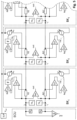
- the Figure 1 shows an example of a tail light module (BLM) of a motor vehicle.
- the tail light module (BLM) has a bus master (ECU) and a serial, bidirectional, differential two-wire communication bus (DB).
- the serial, bidirectional and differential two-wire communication bus (DB) consists of a first single-wire bus (DB a ) and a second single-wire bus (DB b ).
- the TXD and RXD lines of the bus master (ECU) lead to a level converter (TR) to convert the signal level for operating the two-wire communication bus DB.
- the bus master (ECU) receives various control commands from outside, for example for the functions tail light, indicator, rear fog light, dynamic effects, etc., and/or information via a digital bus.
- the bus master converts these commands into bit streams which, among other things, have bits of a synchronization field of the corresponding data frame (bit stream packet (BP)).
- Level converter and bus master are also considered as a unit in the following and are referred to jointly as bus master (ECU).
- bus nodes BK 1 to BK 6 Various components or participants are connected to the communication bus (DB) as bus nodes BK 1 to BK 6.
- the first and second bus nodes ((BK 1 ) and (BK 2 )) are responsible for implementing the flashing light
- the third bus node (BK 3 ) for implementing the tail light
- the fourth and sixth bus nodes (BK 4 ) and (BK 6 ) for executing the brake light function
- the fifth bus node (BK 5) for implementing the reversing light.
- Each of these participants or components has a large number of LEDs (LED 1 to LED 6 ) that are controlled by the respective LED drivers.
- Each bus node is also provided with a digital interface (IF 1 to IF 6 ) in the form of a UART. Furthermore, each bus node has a microcontroller ([ ⁇ C 1 ] to [ ⁇ C 6 ]) and a clock generator ([CLKG 1 ] to [CLKG 6 ]) if required in order to be able to read messages on the differential two-wire communication bus (DB) synchronously with the sending of the bits of the bit streams or to be able to place such bit streams on the two-wire communication bus (DB) synchronously for reading by other participants or the bus master (ECU).
- DB differential two-wire communication bus
- ECU bus master
- the simplification of the hardware of the inventive control of the components of a motor vehicle module is also helped by the fact that fixed sampling points are used at the level of the components or two-wire communication bus participants instead of dynamically adjusting the sampling points.
- the latter is much more complex.
- the clock is generated per participant by reading the synchronization information of the bit streams, which is advantageously sent at the beginning of a bit stream.
- Figure 2 shows a two-wire communication bus (DB) as is known from the prior art.
- the serial, bidirectional, differential two-wire communication bus (DB) consists of a first single-wire bus (DB a ) and a second single-wire bus (DB b ).
- the serial, bidirectional, differential two-wire communication bus connects the bus master (ECU) with several bus nodes ((BK 1 ) to [BK n ]).
- the bus master (ECU) has a first driver [TRa] with which it can bring the first single-wire bus (DB a ) into a first state (Z1) or a second state (Z2) or a third state (Z3).
- a first driver can preferably assume two of three permitted states: In a first state, it applies a first logic level (Z1) to the first single-wire bus (DB a ). In a second state, it applies a third logic level (Z3) to the first single-wire bus (DB a ).
- the first driver of the bus master (ECU) also works in the addressing state of the data bus system and the bus nodes ((BK 1 ) to [BK n' ]) as the first current sink for the first addressing currents of the first addressing current sources ((Iq 1 ) to [Iq n ]) of the bus nodes ((BK 1 ) to [BK n ]) and their first quiescent currents.
- the first driver of a bus node ((BK 1 ) to [BK n ]) or of the bus master (ECU) assumes the first state (Z1) when the second driver [TR b ] of the relevant bus node ((BK 1 ) to [BK n ]) assumes the second state (Z2).
- the signal is differentially impressed with a first differential level (z1).
- the first driver of a bus node ((BK 1 ) to [BK n ]) or of the bus master (ECU) assumes the third state (Z3) when the second driver (TR b ) of the relevant bus node ((BK 1 ) to [BK n ]) assumes the third state (Z3).
- the signal is differentially impressed with a third differential level (z3).
- the first driver can also preferably assume two of two permitted states as an RS485 driver: In a first state, it applies a first logic level (Z1) to the first single-wire bus (DB a ). In a second state, it applies a second logic level (Z2) to the first single-wire bus (DB a ).
- the first driver of the bus master (ECU) also works in the addressing state of the data bus system and the bus nodes ((BK 1 ) to [BK n ]) as the first current sink for the first addressing currents of the first addressing current sources ((Iq 1 ) to [Iq n ]) of the bus nodes ((BK 1 ) to [BK n ]) and their first quiescent currents.
- the first driver of a bus node ((BK 1 ) to [BK n ]) or of the bus master (ECU) assumes the first state (Z1) when the second driver [TR b ] of the relevant bus node ((BK 1 ) to [BK n ]) assumes the second state (Z2).
- the signal is differentially impressed with a first differential level (z1).
- the first driver of a bus node ((BK 1 ) to [BK n ]) or of the bus master (ECU) assumes the second state (Z2) when the second driver [TR b ] of the relevant bus node ((BK 1 ) to [BK n ]) assumes the first state (Z1).
- the signal is differentially impressed with a second differential level (z2).
- the first driver typically has a sub-device for detecting and avoiding a bus collision in the event of simultaneous access to the first single-wire bus (DB a ) by a first driver of another bus node ((BK 1 ) to [BK n ]) or the bus master (ECU).
- a second driver can preferably assume two of three permitted states: In a first state, it applies a second logic level (Z2) to the second single-wire bus (DB b ). In a second state, it applies a third logic level (Z3) to the second single-wire bus (DB b ).
- the second driver of the bus master (ECU) also works in the addressing state of the data bus system and the bus nodes ((BK 1 ) to [BK n ]) as a second current sink for the second addressing currents of the second addressing current sources ((Iq' 1 ) to [Iq' n ]) of the bus nodes ((BK 1 ) to [BK n ]) and their second quiescent currents.
- the second driver of a bus node ((BK 1 ) to [BK n ]) or of the bus master (ECU) assumes the second state (Z2) when the first driver [TR a ] of the relevant bus node ((BK 1 ) to [BK n ]) assumes the first State (Z1).
- the signal is differentially impressed with a first differential level (z1).
- the second driver of a bus node ((BK 1 ) to [BK n ]) or of the bus master (ECU) assumes the third state (Z3) when the first driver [TR a ] of the relevant bus node ((BK 1 ) to (BK n ]) assumes the third state (Z3).
- the signal is differentially impressed with a third differential level (z3).
- the second driver can also, as an RS485 driver, preferably assume two of two permitted states: In a first state, it applies a second logic level (Z2) to the first single-wire bus (DB a ). In a second state, it applies a first logic level (Z1) to the second single-wire bus (DB b ).
- the second driver of the bus master (ECU) also works in the addressing state of the data bus system and the bus nodes ((BK 1 ) to [BK n ]) as a second current sink for the second addressing currents of the second addressing current sources ((Iq' 1 ) to [Iq' n ]) of the bus nodes ((BK 1 ) to [BK n ]) and their second quiescent currents.
- the second driver of a bus node ((BK 1 ) to [BK n ]) or of the bus master (ECU) assumes the second state (Z2) when the first driver [TR a ] of the relevant bus node ((BK 1 ) to [BK n ]) assumes the first state (Z1).
- the signal is differentially impressed with a first differential level (z1).
- the second driver of a bus node ((BK 1 ) to [BK n ]) or of the bus master (ECU) assumes the first state (Z1) when the first driver [TR a ] of the relevant bus node ((BK 1 ) to [BK n ]) assumes the second state (Z2).
- the signal is differentially impressed with a second differential level (z2).
- the second driver typically has a sub-device for detecting and avoiding a bus collision in the event of simultaneous access to the first single-wire bus (DB a ) by a second driver of another bus node ((BK 1 ) to [BK n ]) or the bus master (ECU).
- Each of the bus nodes ((BK 1 ) to [BK n ]) and the bus master (ECU) preferably have a receiver (Rec).
- the respective receiver (Rec) extracts the data (DATA) contained in the bit stream packets (BP) on the serial, bidirectional, differential two-wire communication bus (DB) and outputs them preferably together with error information via an output (out) of the receiver (Rec).
- the receiver (Rec) typically checks whether check information (CHKD) is present within of data information (DATA) of a bit stream packet (BP) indicate error-free reception by the receiver (Rec). If a bit stream packet (BP) was not received error-free by the receiver (Rec), the receiver (Rec) signals this preferentially.
- the data bus system has a common supply voltage line (V bat ) and typically a common reference potential [GND], which is Figure 2 is not shown.
- a device for controlling electrical and/or electronic bus nodes ((BK 1 ) to [BK n ]), in particular within a motor vehicle module, an interior light and/or an exterior light such as a rear light module of a motor vehicle, which device has a serial, bidirectional, differential two-wire communication bus (DB) with n bus nodes (BK 1 to [BK n ]).
- n is a positive integer greater than 1.
- the proposed device also has a bus master (ECU).
- the serial, bidirectional, differential communication bus (DB) consists of a first single-wire bus (DB a ) and a second single-wire bus (DB b ).
- Each bus node (BK j ) of the n bus nodes ((BK 1 ) to [BK n ]) has a differential, serial interface [IF j ] matching the serial, bidirectional, differential communication bus (DB).
- Each bus node (BK j ) of the n bus nodes ((BK 1 ) to [BK n ]) preferably has a clock generator [CLKG j ], a sampling device [AT j ], an address recognition unit [ADR j ] and a bus node address register [BKADR j ].
- the serial, bidirectional, differential communication bus is designed such that it can preferably be in at least a first logical state (high, Z1) and in a second logical state (low, Z2) and possibly in a third logical state (idle, Z3).
- levels of the high-speed CAN protocol [HS-CAN] can be used. This will be explained first.
- the serial, bidirectional, differential communication bus (DB) in the transmitters (TX a , TX b ) of the respective bus node (BK j ) is preferably clamped to a preferably vanishing differential voltage difference between the first single-wire bus (DB a ) and the second single-wire bus (DB b ) corresponding to the third logical state (Idle, Z3) via a high-resistance voltage divider per transmitter (TX a , TX b ).
- Each of the transmitters (TX a , TX b ) preferably comprises a switch with which, when activated, the first single-wire bus (DB a ) of the serial, bidirectional, differential communication bus (DB) is brought to the first logical state (High, Z1) by the first driver [TR a ] and the second single-wire bus (DB b ) of the serial, bidirectional, differential communication bus (DB) can be brought to a second logical state (Low, Z2) by the second driver (TR b ).
- the serial, bidirectional, differential communication bus (DB) in the transmitters (TX a , TX b ) of the respective bus node (BK j ) is preferably clamped to a differential voltage difference corresponding to the third logical state (idle, Z3) via a high-impedance voltage divider per transmitter (TX a , TX b ).
- Each of the transmitters (TX a , TX b ) preferably comprises a half-bridge with which the serial, bidirectional, differential communication bus (DB) can be brought to the first logical state (high, Z1) and a second logical state (low, Z2) by inverse control. If the half-bridges are switched off (IDLE), the serial, bidirectional, differential communication bus (DB) returns to the third logical state (idle, Z3).
- the serial interface (IF j ) of the at least one bus node (BK j ) of the n bus nodes ((BK 1 ) to [BK n ]) is connected to the serial, bidirectional, differential communication bus (DB) in order to send data via this serial, bidirectional, differential communication bus (DB) and/or to receive data from it. It typically comprises the aforementioned transmitters (TX a , TX b ) and a receiver (Rec) for each bus node (BK j ).
- the clock and data extraction within the bus nodes ((BK 1 ) to [BK n ]) from the bit packets (BP) is not shown in the drawings for the sake of simplicity, since it can be taken from the prior art.
- the bus master (ECU) receives external control commands for the n bus nodes ((BK 1 ) to [BK n ]) and converts these control commands into bit streams to be sent to the bus nodes ((BK 1 ) to [BK n ]) via the serial, bidirectional, differential communication bus (DB).
- the bus master (ECU) sends the bits of the bit streams to be sent by the bus master (ECU) via the serial, bidirectional, differential communication bus (DB) depending on a clock pulse (CLK) within the bus master (ECU).
- the bus master (ECU) receives bit streams generated in the opposite direction by the bus nodes ((BK 1 ) to [BK n ]) via the serial, bidirectional, differential communication bus (DB).
- Clock generators [CLKG j ] within each bus node (BK j ) of the n bus nodes ((BK 1 ) to [BK n ]) generate a respective sampling signal [CLKA j ] within each bus node (BK j ) of these bus nodes ((BK 1 ) to [BK n ]).
- the sampling device [AT j ] of this respective bus node (BK j ) of the n bus nodes ((BK 1 ) to [BK n ]) then samples the bit streams sent via the serial, bidirectional, differential communication bus (DB) depending on the sampling signal [CLKA j ] of this bus node (BK j ).
- bus nodes can be bit streams from the bus master (ECU) to the bus nodes ((BK 1 ) to [BK n ]) as well as bit streams from the other bus nodes ((BK 1 ) to [BK n ]) to the bus master (ECU) or to other bus nodes ((BK 1 ) to [BK n ]).
- the bus node in question (BK j ) extracts in this way from the signals on the serial, bidirectional, differential communication bus (DB) a local bit stream within this bus node (BK j ), from the output of the receiver (Rec) by sampling the output signal of the receiver (Rec) or a signal derived from it.
- DB serial, bidirectional, differential communication bus
- the bus master (ECU) sends the bit streams to be sent as sequences of bits in bit stream packets (frames, BP).
- the bus nodes also prefer to send their bit streams as sequences of bits in bit stream packets (frames, BP), which preferably correspond in structure to those of the bus master (ECU). To simplify matters, only the bit stream packets (frames, BP) of the bus master (ECU) are discussed here. The same applies to the bit stream packets (BP) of the bus nodes ((BK 1 ) to [BK n ]).
- this structure means that when neither the bus master (ECU) nor any of the n bus nodes ((BK 1 ) to [BK n ]) transmits data over the serial, bidirectional, differential two-wire communication bus (DB), the serial, bidirectional, differential two-wire communication bus (DB) assumes the first logic state (Z1) (dashed in Figure 3 ) or the third logical state (Z3) - which is preferred.
- V diff represents the differential level on the serial, bidirectional, differential communication bus (DB), i.e. the voltage difference between the first single-wire bus (DB a ) and the second single-wire bus (DB b ).
- HS-CAN describes the corresponding single levels as well as differential levels when CAN drivers [TR a , TR b ] are used.
- RS485 shows the corresponding single levels as well as differential levels when RS485 drivers [TR a , TR b ] are used.
- the drivers [TR a , TR b ] provide three voltage levels in the HS-CAN scheme, but only two differential voltage levels.
- the drivers (TR a , TR b ) provide two voltage levels and only two differential voltage levels in the RS485 scheme.
- the address recognition units ([Adr 1 ] to [Adr n ]) of the bus nodes ((BK 1 ) to [BK n ]) only allow the contained useful information (INFO) to be used if the content of the address information (ADRD) corresponds to the content of the bus node address register [BKADR j ] of the bus node (BK j ).
- the bus nodes (BK j ) of the n bus nodes ((BK 1 ) to [BK n ]) have means for carrying out an auto-addressing method for a two-wire data bus in order to fill the bus node address register [BAKDR j ] with a logical bus node address which corresponds to the physical position of this bus node (BK j ) of the n bus nodes ((BK 1 ) to [BK n ]) within the serial, bidirectional, differential two-wire communication bus (DB).
- BAKDR j bus node address register
- DB serial, bidirectional, differential two-wire communication bus
- each bus node (BK j ) of the n bus nodes has a microcontroller [ ⁇ C j ], which can take over some of the previously mentioned tasks, such as those of the address recognition unit [ADR j ] of the respective bus node (BK j ) and/or the scanning device [AT j ] of the respective bus node (BK j ) via a software program.
- At least one bus node (BK j ) of the n bus nodes ((BK 1 ) to [BK n ]) additionally has at least one light source [LED j ] and at least one energy supply means [EV j ].
- the at least one energy supply means [EV j ] of the at least one bus node (BK j ) of the n bus nodes ((BK 1 ) to [BK n ]) is then provided for the energy supply of the at least one light source [LED j ] of the at least one bus node (BK j ) of the n bus nodes ((BK 1 ) to [BK n ]).
- At least part of the useful information (INFO) includes lighting information (ILD) for controlling the power supply to the lamps [LED j ] of the bus node (BK j ) by the power supply [EV j ] of the bus node (BK j ) depending on this lighting information.
- ILD lighting information
- a lighting register within the power supply [EV j ] is typically written with a value depending on the received lighting information (ILD), which determines the radiation properties such as color, color temperature and brightness of the connected lamps [LED j ].
- the logical content of the address information (ADRD) must match the content of the bus node address register [BKADR j ] of the bus node (BK j ). If this is not the case, the data information (DATA) is ignored.
- the respective address recognition unit [ADR j ] of the respective bus node (BK j ) evaluates the address information (ADRD) of a received bit stream packet (BP) and only allows the contained useful information (INFO) to be used by the rest of the bus node devices of the bus node (BK j ) if the content of the received address information (ADRD) corresponds to the content of the bus node address register [BKADR j ] of the bus node (BK j ) and is error-free.
- bus nodes ((BK 1 ) to [BK n ]) have means for carrying out an auto-addressing method for a serial, bidirectional and differential communication bus (DB).
- DB serial, bidirectional and differential communication bus
- the bus node address register [BAKDR j ] of these bus nodes ((BK 1 ) to [BK n ]) is filled with a logical bus node address that corresponds to the physical position of this bus node (BK j ) of the n bus nodes ((BK 1 ) to [BK n ]) within the serial, bidirectional, differential two-wire communication bus (DB).
- the bus master (ECU) and/or bus nodes ((BK 1 ) to [BK n ]) are equipped with means to conclude, based on the evaluation of the test information (CHKD), that the clock generator [CLKG j ] of one or more bus nodes (BK j ) is not running correctly.
- bus nodes ((BK 1 ) to [BK n ]) independently determine their physical position within the data bus system in the serial, bidirectional, differential two-wire communication bus (DB) and receive a bus node address based on this, so that the logical address corresponds to the physical address.
- DB serial, bidirectional, differential two-wire communication bus
- a first bus shunt resistor (R2) is inserted into the first single-wire bus (DB a ) for each bus node ((BK 1 ) to [BK n ]).
- a second differential amplifier (D2) is used to measure the first current through the first single-wire bus (DB a ) by means of the first shunt resistor (R2).
- the output of the second differential amplifier (D2), which is used to measure the first current through the first single-wire bus (DB a ) is connected to a third comparator (D3), which compares the output value of the second differential amplifier (D2) with a first reference value (Ref).
- the data bus system with its bus nodes ((BK 1 ) to [BK n ]) can now be put into an addressing state and a normal state by the bus master (ECU) using a special bus signal. During the addressing state, an auto-addressing process is carried out. If the data bus system is in the addressing state, the bus nodes ((BK 1 ) to [BK n ]) that can carry out the auto-addressing process are in a corresponding addressing state of the bus nodes.
- the first addressing current source (Iq j ) (with 1 ⁇ j ⁇ n) of the respective bus node (BK j ) is switched off in the normal state or fulfills another function such as supplying power to a light source [LED j ].
- the first addressing current source (Iq j ) (with 1 ⁇ j ⁇ n) of the respective bus node (BK j ) is switched off in the addressing state when the respective bus node (BK j ) detects by means of these first means (R2, D2, D3) a first current through its first bus shunt resistor (R2) which is above a threshold value corresponding to the first reference current [I Ref ].
- the respective first addressing current source (Iq j ) of a bus node (BK j ) feeds its first addressing current into the first single-wire bus (DB a ) before the respective first bus shunt resistor (R2) of the respective bus node (BK j ) as seen from the bus master (ECU), if the bus node (BK j ) determines by means of the first means (R2, D2, D3) described above that only a first current below this threshold value flows through its first bus shunt resistor (R2) in the direction of the bus master (ECU).
- This has the disadvantage that a self-test of the bus node (BK j ) is not possible at this feed-in point of the first addressing current.
- the first driver [TR a ] of the bus master (ECU) can be overloaded during the switch-on process. Therefore, the first Addressing current of the first addressing current sources ((Iq 1 ) to [Iq n ]) is limited to an n-th part of the maximum current value that the first driver [TR a ] can still absorb. This limits the resistance value of the first bus shunt resistor (R2) downwards, since otherwise the level of the voltage drop across the first bus shunt resistor (R2) of a bus node (BK j ) would be too small for detection by the first means (R2, D2, D3) of this bus node (BK j ). This leads to an increased sensitivity to electromagnetic radiation, which is actually to be avoided.
- bus node address to be assigned, typically offered by the bus master (ECU), as its new valid bus node address. Since it then has a valid bus node address, it switches off its addressing current source (Iq j ) and then waits for the end of the addressing state of the data bus system without switching its addressing current source (Iq j ) back on before the end of the addressing state of the data bus system.
- the bus node [BK j-1 ] which is the next bus node to determine in the next initialization run that its addressing current source (Iq j ) is not switched off, then takes the next bus node address to be assigned offered by the bus master (ECU) as its valid bus node address and so on.
- bus nodes ((BK 1 ) to [BK n ]) of the data bus system have received a valid bus node address in this way.
- the bus master then typically returns the data bus system and its bus nodes ((BK 1 ) to [BK n ]) to the normal state, whereby the valid bus node addresses are retained. This recommended retention of the valid bus node addresses when transitioning from the addressing state to the normal state applies preferably to the entire document.
- the serial, bidirectional, differential two-wire communication bus (DB) is a differential bus
- the two single-wire buses (DB a and DB b ) should be designed as symmetrically as possible in order to avoid providing a point of attack for common-mode interference.
- the data bus system should therefore have bus nodes (BK j ) with a first bus shunt resistor ( R2 ) inserted into the first single-wire bus (DB 1 ) for the two-wire communication bus (DB 1 ) and a second single-wire bus (DB 2 ), and a second bus shunt resistor (R2') inserted into the second single-wire bus (DB 2 ).
- the two bus shunt resistors (R2, R2') per bus node (BK j ) of the bus nodes ((BK 1 ) to [BK n ]) are preferably monolithically integrated and manufactured to match with a relative resistance value deviation within the respective bus node (BK j ) of less than 10% and/or better less than 5% and/or better less than 2% and/or better less than 1% and/or better less than 0.5%.
- Each bus node (BK j ) is now equipped, in addition to the first means (R2, D2, D3) for detecting the first current through the first bus shunt resistor (R2) in the first single-wire bus (DB a ), with second means (R2', D2', D3') for detecting the second current through the second bus shunt resistor (R2') in the second single-wire bus (DB b ).
- a second bus shunt resistor (R2') is now inserted into the second single-wire bus (DB b ) for each bus node ((BK 1 ) to [BK n ]).
- a further second differential amplifier (D2') is used to measure the second current through the second single-wire bus (DB b ) using the second shunt resistor (R2') of the relevant bus node (BK j ).
- the output of the further second differential amplifier (D2'), which is used to measure the second current through the second single-wire bus (DB b ), is connected to a further third comparator (D3'), which compares the output value of the further second differential amplifier (D2') with a further reference value (Ref), which is typically equal to the previously mentioned reference value (Ref).
- the second addressing current source (Iq' j ) (with 1 ⁇ j ⁇ n) of the respective bus node (BK j ) is switched off when the respective bus node (BK j ) detects by means of these second means (R2', D2', D3') a first current through its second bus shunt resistor (R2') which is above a threshold value corresponding to the first reference current [I Ref ].
- the respective second addressing current source (Iq' j ) of a bus node (BK j ) feeds the second addressing current, as seen from the bus master (ECU), also upstream of the respective second bus shunt resistor (R2') of the respective bus node (BK j ) into the second single-wire bus (DB b ), if the bus node (BK j ) determines by means of the previously described second means (R2', D2', D3') that only a second current below this threshold value is flowing through its second bus shunt resistor (R2') in the direction of the bus master (ECU).
- both addressing current sources (Iq j , Iq' j ) of a bus node (BK j ) are always switched off when the bus node (BK j ) determines by means of the previously described first means (R2, D2, D3) that a first current above the threshold value flows through its first bus shunt resistor (R2) in the direction of the bus master (ECU) or determines by means of the previously described second means (R2', D2', D3') that only a second current above this threshold value flows through its second bus shunt resistor (R2') in the direction of the bus master (ECU).
- Figure 6 now shows another suggestion based on the Figure 5 .
- Essential difference to Figure 5 is now that the respective first addressing current sources ((Iq 1 ) to [Iq n ]) as seen from the bus master (ECU) feed the first addressing current behind the first bus shunt resistors (R2) in the addressing phase in which the respective bus node (BK j ) is in an addressing state, if the respective bus node (BK j ) determines by means of the first means (R2, D2, D3) a current value of the first current through the first bus shunt resistor (R2) that is smaller than a predetermined first reference current value [I ref ].
- the third comparator (D3) is now preferably a third differential amplifier (D3).
- the respective second addressing current sources ((Iq' 1 ) to [Iq' n ]) as seen from the bus master (ECU) also feed the respective second addressing current behind the corresponding second bus shunt resistors (R2') in the addressing phase in which the respective bus node (BK j ) is in an addressing state, if the respective bus node (BK j ) determines by means of the second means (R2', D2', D3') a current value of the second current through the second bus shunt resistor (R2) that is smaller than a predetermined second reference current value [I' ref ], which is preferably equal to the first reference current value [I ref ].
- the further third comparator (D3') is preferably now a further third differential amplifier (D3').
- the second addressing current of the respective second addressing current source (Iq' j ) of the respective bus node (BK j ) is now also adjusted until the second current through the second bus shunt resistor (R2') corresponds to the predetermined second reference current [I' ref ].
- the bus node (BK j ) is thus provided with a first addressing current source (Iq j ) for determining the bus position of the bus node (BK j ) in the serial, bidirectional, differential two-wire communication bus (DB), which can additionally feed a first addressing current into the first single-wire bus (DB a ) of the serial, bidirectional, differential two-wire communication bus (DB) in a regulated manner such that the first total current (i j ) through the first bus shunt resistor (R2) of the bus node (BK j ) corresponds to a predetermined or calculated or otherwise determined first total current [I ref ].
- the first addressing current preferably flows through the first bus shunt resistor (R2).
- the respective bus node (BK j ) is now provided with a second addressing current source (Iq' j ) for determining the bus position of the bus node (BK j ) in the serial, bidirectional, differential two-wire communication bus (DB), which can additionally feed a second addressing current into the second single-wire bus (DB b ) of the serial, bidirectional, differential two-wire communication bus (DB) in a controlled manner such that the second total current (i j ) through the second bus shunt resistor (R2') of the bus node (BK j ) corresponds to a predetermined or calculated or otherwise determined second total current [I' ref ].
- Iq' j second addressing current source
- the second addressing current now flows through the second bus shunt resistor (R2').
- R2' the second bus shunt resistor
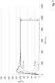
- the Figures 7 to 9 represent advantageous properties of the control.
- the control is explained using the example of the first addressing current sources ((Iq 1 ) to [Iq n ]), but also applies to the second addressing current sources ([Iq' 1 ] to [Iq' n ]) in an analogous manner.
- the units for the abscissa and ordinate are designated with [an] as a placeholder for an arbitrary unit.
- the control characteristic for the first addressing current source (Iq j ) of a bus node (Bk j ) is preferably generated by a first filter (F) or a first controller, which generates a first control signal [rw j ] is generated, with which the first addressing current source (Iq j ) of the relevant bus node (BK j ) is controlled.
- the control characteristic for the second addressing current source (Iq' j ) of a bus node (Bk j ) is preferably generated by a second filter (F') or a second controller, which generates a second control signal (rw' j ) from the output signal of the further third differential amplifier (D3'), with which the second addressing current source (Iq' j ) of the relevant bus node (BK j ) is controlled.
- the time constants for increasing the first addressing current of the first addressing current sources and decreasing the first addressing current of the first addressing current sources are approximately the same. An overshoot occurs.
- the first addressing current (I 1_internal ) of the first addressing current source (Iq 1 ) of the first bus node (BK 1 ) and the first addressing current (I 2_internal ) of the first addressing current source (Iq 2 ) of the second bus node (BK 2 ) are regulated down by the regulators of these first auto-addressing bus nodes, while the first addressing current (I 3_internal ) of the first addressing current source (Iq 3 ) of the third bus node (BK 3 ) is regulated to the reference value [I ref ].
- the settling time is determined by a first time constant [ ⁇ 1 ] for increasing the first addressing current of the first addressing current sources (Iq 1 to Iqs).
- Figure 8 shows the course of the output current (i 1 ) of the first bus node (BK 1 ), the output current (i 2 ) of the second bus node (BK 2 ) and the output current (i 3 ) of the third bus node (BK 3 ). It also shows the current (I 1_internal ) of the first addressing current source (Iq 1 ) of the first bus node (BK 1 ), the current (I 2_internal ) of the first Addressing current source (Iq 2 ) of the second bus node (BK 2 ) and the current (I 3_internal ) of the first addressing current source (Iq 3 ) of the third bus node (BLs).
- the first time constants [ ⁇ 1 ] for the increase in the first addressing current of the first addressing current sources are approximately ten times as long as the second time constants [ ⁇ 2 ] for the decrease in the first addressing current of the first addressing current sources. Only a minimal overshoot occurs.
- Figure 9 shows the course of the output current (i 1 ) of the first bus node (BK 1 ), the output current (i 2 ) of the second bus node (BK 2 ) and the output current (i 3 ) of the third bus node (BK 3 ). It also shows the first addressing current (I 1_internal ) of the first addressing current source (Iq 1 ) of the first bus node (BK 1 ), the first addressing current (I 2_internal ) of the first addressing current source (Iq 2 ) of the second bus node (BK 2 ) and the first addressing current (I 3_internal ) of the first addressing current source (Iq 3 ) of the third bus node (BK 3 ).
- the first time constants [ ⁇ 1 ] for the increase in the first addressing current of the first addressing current sources are approximately one hundred times as long as the second time constants [ ⁇ 2 ] for the decrease in the first addressing current of the first addressing current sources. There is no overshoot.
- the bus node (BK j ) comprises first means (R2, D2) for detecting the current through the first bus shunt resistor (R2) and/or second means (R2', D2') for detecting the current through the second bus shunt resistor (R2').
- the data bus system is designed in such a way that the first and second addressing current of the two addressing current sources (Iq j , Iq' j ) are always fed in behind the bus shunt resistors (R2, R2') as seen from the bus master (ECU), the current detected by the first bus shunt resistor (R2) and/or the second bus shunt resistor (R2') can be used for a self-test.
- both voltage drops across both bus shunt resistors (R2, R2') should preferably be the same.
- a cold solder joint for example, can be easily detected in this way.
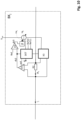
- the bus node (BK j ) with a first detection device (DET) that checks the internal signals (ds1, ds3) of the bus node (BK j ) for plausibility.
- the internal signals are preferably control signals within the bus node (BK j ).
- bus symmetry for example, the symmetry of these signals can be checked.
- tests per channel are also possible.
- the first detection device changes the feed point for the first addressing current of the regulated first addressing current source (Iq j ) of the j-th bus node (BK j ), for example with the aid of a first analog demultiplexer (X3), and swaps the polarity of the inputs or the output of the second differential amplifier (D2) by means of the polarity signal (pol).
- the second detection device (DET') can, for example, change the feed point for the second addressing current of the regulated second addressing current source (Iq' j ) of the j-th bus node (BK j ), for example with the aid of a second analog demultiplexer (X3'), and swap the polarity of the inputs or the output of the further second differential amplifier (D2') by means of a second polarity signal (pol').
- a reparameterization of internal sub-devices such as current sources for neutralizing the error is possible if, instead of a first addressing current source (Iq j ) of the j-th bus node (BK j ) and a first multiplexer (X3), a first addressing current source [Iq j1 ] of the j-th bus node (BK j ) and, for example, a further first addressing current source [Iq j2 ] of the j-th bus node (BK j ) are used, of which the first addressing current source [Iq j1 ] of the j-th bus node (BK j ) feeds its first addressing current before the first bus shunt resistor (R2) and the further first addressing current source [Iq j2 ] of the j-th bus node (BK j ) feeds its further first addressing current behind the first bus shunt resistor (
- the first detection device would set the first addressing current of one of the two first addressing current sources ([Iq j1 ], [Iq j2 ]) to zero, so that the equivalent effect as with the combination of a first addressing current source (Iq j ) of the j-th bus node (BK j ) with the switching by a first demultiplexer (X3).
- a second addressing current source [Iq' j1 ] of the j-th bus node (BK j ) and, for example, a further second addressing current source [Iq' j2 ] of the j-th bus node (BK j ) would be used, of which the second addressing current source [Iq' j1 ] of the j-th bus node (BK j ) feeds its second addressing current upstream of the second bus shunt resistor (R2') and the further second addressing current source [Iq' j2 ] of the j-th bus node (BK j ) feeds its further second addressing current downstream of the second bus shunt resistor (R2').
- the second detection device would set the second addressing current of one of the two second addressing current sources ([Iq' j1 ], [Iq' j2 ]) to zero, so that the equivalent effect is achieved as in the combination of a second addressing current source (Iq' j ) of the j-th bus node (BK j ) with the switching by a further second demultiplexer (X3').
- the first detection device can recognize that the first control value of the first control signal (rw j ) of the j-th bus node (BK j ) maximizes the first addressing current of the first addressing current source (Iq j ). This can be done, for example, with a suitable design, by comparing the first control value of the first control signal (rw j ) with a tenth threshold value (Ref10). If the derivative of the first addressing current of the first auto-addressing current source (Iq j ) with respect to the first control value of the first control signal (rw j ) is positive, this means that the first control value of the first control signal (rw j ) is above the tenth threshold value (Ref10).
- the first detection device (DET) can simultaneously compare the output (ds2) of the second differential amplifier (D2) with an eleventh threshold value (Ref11). If the value of the output (ds2) of the second differential amplifier (D2) is below the eleventh threshold value (Ref11), the first detection device (DET) can conclude that there is a negative voltage drop across the first bus shunt resistor (R2) or that there is a voltage drop across the first bus shunt resistor (R2) close to zero. This state is illegal because the first auto-addressing current source (Iq j ) supplies a positive first addressing current which, if correctly assembled, should flow through the first bus shunt resistor (R2), but this obviously does not happen.
- Iq j the first auto-addressing current source
- the second detection device (DET') can also detect that the second control value of the second control signal (rw' j ) of the j-th bus node (BK j ) maximizes the second addressing current of the second addressing current source (Iq' j ). This can be done, for example, with a suitable design, by comparing the second control value of the second control signal (rw' j ) with a further tenth threshold value (Ref10'), which is preferably equal to the tenth threshold value (Ref10).
- the second detection device (DET) can simultaneously compare the further output (ds2') of the further second differential amplifier (D2') with a further eleventh threshold value (Ref11').
- the further eleventh threshold value (Ref11') is preferably equal to the eleventh threshold value (Ref11).
- the second detection device can conclude that there is a negative voltage drop across the second bus shunt resistor (R2') or that there is a voltage drop across the second bus shunt resistor (R2') close to zero.
- This state is illegal because the second auto-addressing current source (Iq' j ) supplies a positive second addressing current which, if correctly mounted, should flow through the second bus shunt resistor (R2'), but this obviously does not happen.
- the first detection device (DET) and the second detection device (DET) form a unit.
- a change of the bus direction preferably only occurs when both detection devices (DET, DET) detect a swap of the bus connections.
- the detection devices can signal a detected error, for example, via a respective error signal (er, er') to a bus node internal computer or a suitable controller.
- the test results can be used by the bus node (BK j ) or a sub-device (DET, DET) of the bus node (BK j ) to initiate and take predetermined measures if one or more of the detection devices (DET, DET) detect implausible internal signals within the bus node (BK j ).
- the bus node (BK j ) can assume that the input and output have been swapped.
- the bus node (BK j ) has a first sub-device (X3) which can change the feed point of the first addressing current of the first addressing current source (Iq j ) and/or if the bus node (BK j ) has a second sub-device (X3') which can change the feed point of the second addressing current of the second addressing current source (Iq' j ).
- the changes for controlling the first single-wire bus (DB a ) and the first bus shunt resistor (R2) are carried out synchronously with the analog changes for controlling the second single-wire bus (DB b ) and the second bus shunt resistor (R2').
- Such a bus node (BK j ) therefore has, instead of a first addressing current source (Iq j ), a first addressing current source and a further first addressing current source, the first addressing current source feeding its first addressing current into a node connected to the first terminal of the first bus shunt resistor (R2) when it feeds in current, and the further first addressing current source feeding its first addressing current into a node connected to the second terminal of the first bus shunt resistor (R2) when it feeds in current.
- the two first addressing current sources preferably feed their addressing currents in such a way that the resulting total addressing current flows through the first bus shunt resistor (R2), which ensures the self-test capability.
- the bus node (BK j ) further comprises, instead of a second addressing current source, a second addressing current source and a further second addressing current source, wherein the second addressing current source feeds its addressing current into a node connected to the first terminal of the second bus shunt resistor (R2') when it feeds current, and wherein the further second addressing current source feeds its addressing current into a node connected to the second terminal of the second bus shunt resistor (R2') connected nodes when it injects current.
- These two second addressing current sources also preferentially inject their addressing currents so that the addressing current flows through the second bus shunt resistor (R2') to ensure self-test capability.
- the first addressing current source (Iq j ) increases the first addressing current with a first time constant [ ⁇ 1 ] and decreases it with a second time constant [ ⁇ 2 ] which is smaller than the first time constant [ ⁇ 1 ] and/or if the second addressing current source (Iq' j ) increases the second addressing current with a third time constant [ ⁇ 3 ] and decreases it with a fourth time constant [ ⁇ 4 ] which is smaller than the third time constant [ ⁇ 3 ].
- the third time constant [ ⁇ 3 ] and the first time constant [ ⁇ 1 ] are preferably chosen to be the same amount in order to ensure bus symmetry dynamically too.
- the fourth time constant [ ⁇ 4 ] and the second time constant [ ⁇ 2 ] are preferably chosen to have the same amount in order to ensure dynamic bus symmetry here too.
- the bus node (BK j ) described above is therefore a bus node (BK j ) which is capable of carrying out a method for assigning bus addresses to bus nodes of a serial, bidirectional, differential two-wire communication bus (DB).
- the method for assigning bus addresses to bus nodes ((BK 1 ), (BK 2 ), (BK 3 ), whil [BK n-1 ], [BK n ]) of a serial, bidirectional, differential two-wire communication bus (DB) is carried out with the aid of first bus shunt resistors (R2) and with the aid of second bus shunt resistors (R2') in the individual bus nodes ((BK 1 ), (BK 2 ), (BK 3 ), «
- the bus node (BK j ) is thus preferably characterized compared to the prior art by such a first bus shunt resistor (R2) and such a second bus shunt resistor (R2').
- the bus node (BK j ) is each provided with a first bus shunt bridging switch (S4) which is open before a bus address is assigned to the bus node (BK j ) in the assignment period and which is closed after a bus address is assigned to the bus node in the assignment period and which is closed in the operating period.
- a second bus shunt bridging switch (S4') is preferably provided in the bus node (BK j ), which is open before a bus address is assigned to the bus node (BK j ) in the assignment period and which is closed after a bus address is assigned to the bus node (BK j ) in the assignment period and which is closed during the operating period.
- These bus shunt bridging switches (S4, S4') massively reduce the bus resistance and reduce the sensitivity to electromagnetic radiation. They therefore improve the EMC behavior.
- a common-mode current source [GLIq j ] of a bus node (BK j ) with two outputs can also be used, both of which feed the same amount of common-mode current into the first single-wire bus (DB a ) and the second single-wire bus (DB b ) of the serial bidirectional differential communication bus (DB) with the same sign.
- a first output of these two outputs therefore corresponds to the first addressing current source (Iq j ).
- the second output then corresponds to the second addressing current source (Iq' j ).
- the first addressing current of the first addressing current source (Iq j ) is then equal in amount to the second addressing current of the second addressing current source (Iq' j ).
- the use of a single common-mode addressing current source [GLIq j ] has the advantage that only one control loop is required.
- a push-pull current source [GGIq j ] of a bus node (BK j ) with two outputs can also be used, both of which feed the same amount of push-pull current into the first single-wire bus (DB a ) and the second single-wire bus (DB b ) of the serial bidirectional differential communication bus (DB), but now with a different sign.
- a first output of these two outputs therefore corresponds to the first addressing current source (Iq j ).
- the second output then corresponds again to the second addressing current source (Iq' j ).
- the first addressing current of the first addressing current source (Iq j ) is then equal in amount but not the same in sign as the second addressing current of the second addressing current source (Iq' j ).
- the use of a single push-pull addressing current source[GLIq j ] also has the advantage that only one control loop is required.
- a bus node (BK j ) for a serial, bidirectional, differential two-wire communication bus (DB) with a bus master (ECU) is also proposed here, in which the serial, bidirectional, differential two-wire communication bus (DB) comprises a first single-wire bus (DB 1 ) and a second single-wire bus (DB 2 ).
- a first bus shunt resistor (R2) inserted into the first single-wire bus (DB 1 ) and a second bus shunt resistor (R2') inserted into the second single-wire bus (DB 2 ) are part of the bus node (BK j ).
- the bus node further comprises a differential first common-mode addressing current source [GLIq j ] for determining the bus position of the bus node (BK j ) in the serial, bidirectional, differential two-wire communication bus (DB).
- the differential first common-mode addressing current source [GLIq j ] can additionally feed a first common-mode addressing current component into the first single-wire bus (DB a ) of the serial, bidirectional, differential two-wire communication bus (DB) in a controlled manner such that the first total current (i j ) through the first bus shunt resistor (R2) of the bus node (BK j ) corresponds to a predetermined or calculated or otherwise determined first total current [I ref ].
- the differential first common-mode addressing current source [GLIq j ] can additionally feed a second common-mode addressing current component with the same amount and sign into the second single-wire bus (DB b ) of the serial, bidirectional, differential two-wire communication bus (DB) in a regulated manner with the same sign as the sign of the first differential-mode addressing current component, so that the second total current (i' j ) through the second bus shunt resistor (R2') of the bus node (BK j ) also corresponds to the predetermined or calculated or otherwise determined first total current [I ref ].
- the first common-mode addressing current component of the common-mode addressing current source [GLIq j ] of the bus node (BK j ) flows through the first bus shunt resistor (R2) of the bus node (BK j ) in the direction of the bus master (ECU).
- the second common-mode addressing current component of the common-mode addressing current source [GLIq j ] of the bus node (BK j ) flows through the second bus shunt resistor (R2') of the bus node (BK j ) in the direction of the bus master (ECU).
- a bus node (BK j ) for a serial, bidirectional, differential two-wire communication bus (DB) with a bus master (ECU) is therefore proposed, in which the serial, bidirectional, differential two-wire communication bus (DB) comprises a first single-wire bus (DB 1 ) and a second single-wire bus (DB 2 ) and in which a first bus shunt resistor (R2) is inserted into the first single-wire bus (DB 1 ) and a second bus shunt resistor (R2') is inserted into the second single-wire bus (DB 2 ).
- the bus node (BK j ) then has a differential first push-pull addressing current source [GGIq j ] for determining the bus position of the bus node (BK j ) in the serial, bidirectional, differential two-wire communication bus (DB), which feeds a first push-pull addressing current component in the first single-wire bus (DB a ) of the serial, bidirectional, differential two-wire communication bus (DB) in a controlled manner so that the first total current (i j ) through the first bus shunt resistor (R2) of the bus node (BK j ) corresponds to a predetermined or calculated or otherwise determined first total current [I ref ].
- GGIq j differential first push-pull addressing current source
- the push-pull addressing current source [GGIq j ] of the bus node (BK j ) feeds the second push-pull addressing current component, which is the same in magnitude, additionally into the second single-wire bus (DB b ) of the serial, bidirectional, differential two-wire communication bus (DB) in a regulated manner with the opposite sign to the sign of the first push-pull addressing current component, so that the second total current (i' j ) through the second bus shunt resistor (R2') of the bus node (BK j ) also corresponds to the predetermined or calculated or otherwise determined first total current [I ref ].
- the first push-pull addressing current component of the push-pull addressing current source [GGIq j ] of the bus node (BK j ) flows through the first bus shunt resistor (R2) of the bus node (BK j ) in the direction of the bus master (ECU).
- the second push-pull addressing current component of the push-pull addressing current source [GGIq j ] of the bus node (BK j ) flows through the second bus shunt resistor (R2') of the bus node (BK j ) in the direction of the bus master (ECU).
- the bus node (BK j ) preferably has first means (R2, D2) to detect the current through the first bus shunt resistor (R2) and/or second means (R2', D2') to detect the current through the second bus shunt resistor (R2').
- the ability to detect the voltage drop across the respective bus shunt resistor (R2, R2') can also be used for a self-test.
- a bus node (BK j ) is therefore proposed in which the detected current through the first bus shunt resistor (R2) is used for a self-test and/or in which the detected current through the second bus shunt resistor (R2') is used for a self-test.
- the detected voltage drop across the bus shunt resistor is compared with an expected value. If the detected voltage deviates from the expected value by more than a predetermined amount, an error has occurred that can be signaled.
- the proposed bus node (BK j ) preferably comprises at least one detection device (DET) which checks internal signals (ds1, ds3) of the bus node (BK j ) for plausibility.
- the bus node (BK j ) or a sub-device (DET) of the bus node (BK j ) measures if the detection device (DET) detects implausible internal signals within the bus node (BK j ).
- One possible measure can be initiated by a first sub-device (X3) of the bus node (BK j ) and a second sub-device (X3') of the bus node (BK j ) in such a way that the feed points of the first common-mode addressing currents of the common-mode addressing current source [GLIq j ] are changed by the first sub-device (X3) of the bus node (BK j ) and the second sub-device (X3') of the bus node (BK j ) when a predetermined error is detected.
- Another possible measure can be initiated by a first sub-device (X3) of the bus node (BK j ) and a second sub-device (X3') of the bus node (BK j ) in such a way that the feed points of the first push-pull addressing currents of the push-pull addressing current source [GGIq j ] are changed by the first sub-device (X3) of the bus node (BK j ) and the second sub-device (X3') of the bus node (BK j ) upon detection of a predetermined error.
- a bus node (BK j ) is therefore proposed in which the common-mode addressing current source [GLIq j ] increases the common-mode addressing current with a first time constant [ ⁇ 1 ] and decreases it with a second time constant [ ⁇ 2 ] which is smaller than the first time constant [ ⁇ 1 ].
- a bus node (BK j ) is therefore proposed in which the push-pull addressing current source [GGIq j ] increases the push-pull addressing current with a first time constant [ ⁇ 1 ] and decreases it with a second time constant [ ⁇ 2 ] which is smaller than the first time constant [ ⁇ 1 ].
- bus node (BK j ) which is intended for a data bus system with a serial, bidirectional, differential two-wire communication bus (DB), can be used for another auto-addressing method (see Figure 13 ) are prepared.
- the bus node (BK j ) in question is then again intended to participate in a process to participate in the allocation of logical bus node addresses to the bus nodes ((BK 1 ) to [BK n ]) of the data bus system.
- the corresponding data bus system then has a bus master (ECU) with an address input (Adr i0 ).
- the data bus system should in turn have n bus nodes ((BK 1 ) to [BK n ]) including this bus node (BK j ) itself, with n as a positive integer.
- the bus node (BK j ) is connected to the bus master (ECU) for data transmission via a data line section ((DB 1 ) to [DB n ]) or the serial, bidirectional, differential two-wire communication bus (DB) consisting of data line sections ((DB 1 ) to [DB n ]) and further bus nodes ((BK 2 ) to [BK n ]).
- a line [L 1 to L n ] is looped from an address input (Adr i0 ) of the bus master (ECU) of the data bus system through all bus nodes ((BK 1 ) to [BK n ]) of the data bus system, including this bus node (BK j ) itself, in such a way that it is divided into n line sections [L 1 to L n ] by the individual bus nodes ((BK 1 ) to [BK n ]), including this bus node (BK j ) itself.
- Each of the bus nodes (BK j ) comprises an associated address input [Adr ij ] and an address output [Adr oj ] associated with this bus node (BK j ).
- the bus node address of the bus node (BK j ) in its bus node address register [BKADR j ] can be valid or invalid, as in this entire document.
- the proposed bus node now provides means and methods to set its bus node address and to make its bus node address valid or invalid.
- the proposed bus node (BK j ) can assume an addressing state and a second operating state (or normal state) that is different from the addressing state.
- the bus node (BK j ) preferably has means for switching between the addressing state and the second operating state depending on commands from the bus master (ECU).
- the bus node (BK j ) then has means, when it is in the addressing state and when its bus node address is invalid, in this case to set the logical state at the address input [Adr i(j-1) ] of a preceding bus node [BK j-1 ] to a first logical value by overwriting, or, when it is in the addressing state and when its bus node address is invalid, in this case to set the logical state at the address input (Adr i0 ) of a preceding bus master (ECU) to a first logical value by overwriting.
- the bus node (BK j ) preferably further comprises means for setting the logical state at its address input [Adr ij ] to a second logical value in the addressing state if this second logical value is not overwritten by a subsequent bus node [BK j+i ] with a first logical value, and means for adopting a bus node address signaled by the bus master (ECU) as its valid future bus node address if its bus node address is invalid and if it is in the addressing state and if its address input [Adr ij ] has a second logical value, and for marking this future bus node address as "valid" in this case.
- the address input [Adr ij ] of the bus node (BK j ) in the second operating state can be used as the input of an interrupt signal of a subsequent bus node [BK j-1 ].
- an interrupt line can be used for the auto-addressing of bus nodes of a serial, bidirectional, differential two-wire communication bus (DB).
- the address output [Adr oj ] of the bus node (BK j ) in the second operating state can be used as the output of an interrupt signal of a subsequent bus node [BK j-1 ] and/or of the bus node (BK j ) itself.
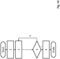
- Figure 14 describes the basic sequence of the preferred address allocation procedure described here.
- the bus master (BM) signals in a first method step (1) by means of a preferred first broadcast command preferably to a bus node or preferably to all or at least a part of the set of bus nodes ((BK 1 ) to [BK n ]) that such a procedure for allocating bus node addresses for these bus nodes has been started. This preferably results in all these bus nodes ((BK 1 ) to [BK n ]) invalidating or deleting any valid bus node addresses present in these bus nodes.
- this interrupt line [L 1 to L n ] loses this function for the duration of the addressing process and is split into the said point-to-point connections between the bus nodes ((BK 1 ) to [BK n ]) and the point-to-point connection between the first LED bus node (BK 1 ) and the bus master (BM).
- the bus master (ECU) informs the bus nodes ((BK 1 ) to [BK n ]) that a bus node address is to be assigned and which logical bus node address this is.
- the bus node here arbitrarily the j-th bus node (BK j ) as an example for greater clarity, whose address input [Adr ij ] has a second logical value, then takes over the bus address offered by the bus master (BM) in this process step and sets its address output [Adr oj ] in such a way that it no longer overwrites the address input [Adr i(j-1) ] of a preceding bus node [BK j-1 ] to the first logical value, but allows a second logical value at the address input [Adr i(j-1) ] of a preceding bus node [BK j-1 ].
- This second logical value is then preferably impressed by the preceding bus node [BK j-1 ] itself at its address input [Adr i(j-1) ].
- the bus master (ECU) checks whether the logical value at its address input (Adr i0 ) corresponds to a second logical value or not. If it does not correspond to this (N), the bus master (ECU) repeats the second process step (2). If it corresponds to this logical value (J), the bus master (ECU) ends the process by carrying out a fourth process step (4). If necessary, it first carries out a check to ensure that the allocation has been correct.
- the bus master preferably sends a message to all bus nodes ((BK 1 ) to [BK n ]) that the bus node addresses have been allocated.
- the bus nodes ((BK 1 ) to [BK n ]) change from the addressing state assumed in the first process step (1) to another operating state, preferably the normal operating state or normal state.
- the bus nodes ((BK 1 ) to [BK n ]) use a looped interrupt line that may have been used for the point-to-point connections as an interrupt line again. This concludes the proposed procedure as such (END).
- the data bus system comprises a bus master (ECU), a serial, bidirectional, differential two-wire communication bus (DB) originating from the bus master (ECU), and a plurality of addressable bus nodes ((BK 1 ) to [BK n ]) connected to the serial, bidirectional, differential two-wire communication bus (DB).
- the serial, bidirectional, differential two-wire communication bus (DB) consists of the said first single-wire bus (DB a ) and the said second single-wire bus (DB b ).
- Each bus node (BK j ) of the bus nodes ((BK 1 ) to [BK n ]) that has not yet been addressed does not have a valid bus node address and therefore feeds a first addressing current into the first single-wire bus (DB a ) and a second addressing current into the second single-wire bus (DB b ) for identification purposes. All of these addressing currents flow through the serial, bidirectional, differential two-wire communication bus (DB) in the direction of the bus master (ECU).
- DB serial, bidirectional, differential two-wire communication bus
- Each bus node (BK j ) that has not yet been addressed detects the first current flowing through the first single-wire bus (DB a ) of the serial, bidirectional, differential two-wire communication bus (DB) and the second current flowing through the second single-wire bus (DB b ) of the serial, bidirectional, differential two-wire communication bus (DB).
- DB a first single-wire bus
- DB b second single-wire bus
- DB b second single-wire bus
- the bus node identified in this way is assigned an address for the purpose of addressing, whereby it receives a valid bus node address.
- the aforementioned steps are carried out without the bus node addressed last until all of the as yet unaddressed bus nodes have been addressed.
- the first threshold value is equal to the further first threshold value and the value of the first addressing current within a bus node is equal to the value of the second addressing current within this bus node.
- unaddressed bus nodes without a valid bus node address can also be connected to the serial, bidirectional, differential two-wire communication bus (DB).
- the unaddressed bus node feeds a first quiescent current into the first single-wire bus (DB a ) and a second quiescent current into the second single-wire bus (DB b ).
- DB a first single-wire bus
- DB b second quiescent current into the second single-wire bus
- each bus node that has not yet been addressed detects the first quiescent current flowing through the first single-wire bus (DB a ) and the second quiescent current flowing through the second single-wire bus (DB b ).
- the bus node identified in this way is assigned an address for the purpose of addressing, whereby it receives a valid bus node address. The previously mentioned steps are carried out without the bus node that was last addressed until all the bus nodes that have not yet been addressed have been addressed.
- the second threshold value is preferably equal to the first threshold value or the further first threshold value.
- each addressable bus node feeds a first quiescent current, which can be zero, into the first single-wire bus (DB a ), and a second quiescent current, which can be zero, into the second single-wire bus (DB b ).
- DB a first single-wire bus
- DB b second single-wire bus
- Each as yet unaddressed bus node without a valid bus node address feeds a first quiescent current into the first single-wire bus (DB a ) and a second quiescent current into the second single-wire bus (DB b ).
- Each as yet unaddressed bus node detects the first current flowing through the first single-wire bus (DB a ) due to the quiescent current feed, and the second current flowing through the second single-wire bus (DB b ) due to the quiescent current feed. In this process, it is determined which of the as yet unaddressed bus nodes detects a first current that is above a predefinable third threshold value, and which of the as yet unaddressed bus nodes detects a second current that is above a predefinable further third threshold value.
- first addressing currents are fed into the first single-wire bus (DB a ), and only those bus nodes that have not yet been addressed and which, when the quiescent currents are fed in, detect a second current that is less than the third threshold value or equal to the third threshold value, preferably feed second addressing currents into the second single-wire bus (DB b ).
- the bus node that does not detect a first current or only a first current that is less than a predefinable fourth threshold value and that does not detect a second current or only a second current that is less than a predefinable further fourth threshold value is identified as a not yet addressed bus node.
- the bus node identified in this way is assigned an address for the purpose of addressing.
- the previously mentioned steps are carried out without the bus node that was addressed last until all the not yet addressed bus nodes have been addressed.
- the third and/or fourth threshold value and/or the further third and/or further fourth threshold value and the first threshold value are the same.
- non-addressable bus nodes are connected to the serial, bidirectional, differential two-wire communication bus (DB) in addition to the addressable bus nodes.
- DB serial, bidirectional, differential two-wire communication bus
- Such a non-addressable bus node feeds a first quiescent current into the first single-wire bus (DB a ) and a second quiescent current into the second single-wire bus (DB b ).
- DB a Before feeding the first addressing currents into the first single-wire bus (DB a ), each bus node that has not yet been addressed determines the first current flowing in the first single-wire bus (DB a ) due to the quiescent current feed of all non-addressable bus nodes by means of a first current detection.
- each bus node that has not yet been addressed determines the first current flowing in the second single-wire bus (DB b ) due to the quiescent current feed of all non-addressable bus nodes by means of a first current detection. addressable bus nodes through a second current detection. Each addressable bus node then feeds a first quiescent current into the first single-wire bus (DB a ) and a second quiescent current into the second single-wire bus (DB b ).
- the bus node that detects no current difference of the first current compared to the first current detection or only a current difference of the first current that is smaller than a predefinable sixth threshold value, and that detects no current difference of the second current compared to the first current detection or only a current difference of the second current that is smaller than a predefinable sixth threshold value is identified as a not yet addressed bus node.
- the bus node identified in this way is assigned an address for the purpose of addressing. The previously mentioned steps are carried out without the bus node that was last addressed until all the not yet addressed bus nodes have been addressed.
- the fifth threshold value and/or the sixth threshold value and/or the further fifth threshold value and/or the further sixth threshold value and/or the first threshold value are preferably equal.
- the first current detection preferably takes place in the bus node via the first bus shunt resistors (R2) of the first single-wire bus (DB a ) assigned to the addressable bus node
- the second current detection preferably takes place in the bus node via the second bus shunt resistors (R2') of the second single-wire bus (DB b ) assigned to the addressable bus node.
- the first bus shunt resistors (R2) assigned to an addressable bus node preferably correspond to the second bus shunt resistors (R2') assigned to the respective addressable bus node, at least in terms of value.
- All first bus shunt resistors (R2) are preferably connected in series in the first single-wire bus (DB a ) along the first single-wire bus (DB a ) and all second bus shunt resistors (R2') are preferably connected in series in the second single-wire bus (DB b ) along the second single-wire bus (DB b ).
- voltage detection can also be carried out in the bus nodes.
- the assignment of an address is then typically carried out by transmitting an address to the identified bus node in such a way that the same address is transmitted to all bus nodes that have not yet been addressed before a bus node is identified and only the subsequently identified bus node accepts this address as its bus node address.
- the assignment of an address takes place after the first identification of a bus node and/or a verification of the bus node address after the identification of a bus node.
- the identification of a bus node can be verified, for example, by identifying the bus node again and/or by identifying the bus node using the other single-wire bus and comparing the second identification with the first identification.
- the verification of the identification of a participant can also be carried out by identifying the participant again using another auto-addressing method and The second identification is compared with the first identification. Any errors that occur are signalled.
- the data bus system has a bus master (ECU), a serial, bidirectional, differential two-wire communication bus (DB) originating from the bus master (ECU), and a plurality of addressable bus nodes ((BK 1 ) to [BK n ]) connected to the serial, bidirectional, differential two-wire communication bus (DB).
- the serial, bidirectional, differential, two-wire communication bus (DB) again consists of a first single-wire bus (DB a ) and a second single-wire bus (DB b ).
- each bus node (BK j ) of the bus nodes ((BK 1 ) to [BK n ]) that has not yet been addressed feeds an addressing current into at least ONE single-wire bus of the single-wire buses (DB a , DB b ) for identification.
- Each bus node that has not yet been addressed feeds the addressing current into at least one single-wire bus, referred to below as the addressing single-wire bus.
- this addressing current is fed into both single-wire buses (DB a , DB b ). All other bus nodes that have not yet been addressed also feed their respective addressing current into the addressing single-wire bus.
- All addressing currents flow through the serial, bidirectional, differential two-wire communication bus (DB) in the direction of the bus master (ECU).
- Each bus node that has not yet been addressed (BK j ) detects the current flowing through the addressing single-wire bus of the serial, bidirectional, differential two-wire communication bus (DB). This detection preferably takes place via the bus shunt resistors (R2, R2') mentioned above.
- R2, R2' bus shunt resistors
- Only the bus node (BK j ) that has not yet been addressed and that detects no current or only a current that is less than a predeterminable first threshold value is identified as a bus node that has not yet been addressed.
- the bus node identified in this way is assigned an address for addressing purposes, which gives it a valid bus node address. This is preferably determined by the bus master (ECU). The previously mentioned steps are carried out again without the last bus node addressed, i.e. another initialization run is carried out until all bus nodes
- non-addressed bus nodes are connected to the serial, bidirectional, differential two-wire communication bus (DB), which feed a quiescent current into the addressing single-wire bus.
- DB serial, bidirectional, differential two-wire communication bus
- each non-addressed bus node detects the quiescent current flowing through the addressing single-wire bus before feeding in the addressing currents. Only the non-addressed bus nodes feed the addressing currents into the addressing single-wire bus.
- the bus node identified in this way is assigned an address for addressing purposes, which gives it a valid bus node address. The steps mentioned above are carried out without the last addressed bus node until all bus nodes that have not yet been addressed are addressed.
- the second threshold value is preferably equal to the first threshold value.
- Every addressable bus node feeds a quiescent current into the addressing single-wire bus, and that every bus node that has not yet been addressed feeds a quiescent current into the addressing single-wire bus.
- the process is then modified in a similar way to that described above: every bus node that has not yet been addressed again detects the current flowing through the addressing single-wire bus due to the quiescent current feed.
- a circuit within the bus nodes (BK j ) then determines which of the bus nodes that have not yet been addressed detects a current that is above a predeterminable third threshold value.
- the third and/or fourth threshold value is the same as the first threshold value.
- each non-addressable bus node is connected to the serial, bidirectional, differential two-wire communication bus (DB), which feeds a quiescent current into the addressing single-wire bus.
- DB serial, bidirectional, differential two-wire communication bus
- the method is modified appropriately: Before feeding in the addressing currents, each bus node that is not yet addressed determines the current flowing in the addressing single-wire bus due to the quiescent current feed of all non-addressable bus nodes by means of a first current detection. Then each addressable bus node feeds a quiescent current into the addressing single-wire bus. It is then determined which of the bus nodes that are not yet addressed detects a current that is above a predefinable fifth threshold value.
- the current detection in the bus nodes preferably takes place via the shunt resistors of the addressing single-wire bus assigned to the addressable bus nodes, whereby in the other single-wire bus, which is not the addressing single-wire bus, further bus shunt resistors assigned to the addressable participants are preferably, but not necessarily, arranged in the participants, which preferably correspond in value to the shunt resistors in the addressing single-wire bus.
- the bus shunt resistors (R2, R2') in the two single-wire buses (DB a , DB b ) particularly preferably match each other. All shunt resistors in the addressing single-wire bus along the addressing single-wire bus are preferably connected in series. All shunt resistors in the other single-wire bus along this other single-wire bus are also preferably connected in series.
- a variant of the method provides that the assignment of an address takes place by transmitting an address to the identified bus node or by transmitting the same address to all bus nodes that have not yet been addressed before a bus node is identified and that only the subsequently identified bus node accepts this address as its bus node address.
- a further variant of the proposed method provides that the assignment of an address takes place after the first identification of a bus node or that a verification of the bus node address takes place after the identification of a bus node.
- a further variant of the proposed method provides that the verification of the identification of a bus node is carried out by identifying the bus node again and/or by identifying the bus node by means of the other single-wire bus and comparing the second identification with the first identification.
- Another variant of the proposed method provides that the identification of a participant is verified by identifying the participant again using a different auto-addressing method and comparing the second identification with the first identification.
- the bus node and/or the bus master then signal an error.
- This basic method can be supplemented with an additional step after or together with the acceptance of the bus node address to be assigned. It then includes bridging the first bus shunt resistor (R2) using a first bus shunt bridging switch (S4) and/or bridging the second bus shunt resistor (R2') using a second bus shunt bridging switch (S4') when changing from the addressing state with an invalid bus node address of the respective bus node (BK j ) to the addressing state with a valid bus node address of the respective bus node (BK j ) or when changing to the normal state.
- This procedure has the advantage that the bus resistance is reduced during operation (normal state after address assignment).
- the bridging of the bus shunt resistors (R2, R2') is reversed.
- the method then comprises opening the first bus shunt bridging switch (S4) if the bus node address of the relevant auto-addressing bus node (BK j ) is not valid and/or opening the second bus shunt bridging switch (S4') if the bus node address of the relevant auto-addressing bus node (BK j ) is not valid.
- the third time constant [ ⁇ 3 ] is preferably chosen to be smaller than the first time constant [ ⁇ 1 ] and the second time constant [ ⁇ 2 ] by a factor of more than 10.
- the third time constant ⁇ 3 preferably depends in a method variant within the relevant auto-addressing bus node (BK j ) on the first value of the first bus node output current (i j ) of the relevant auto-addressing bus node (BK j ) detected by means of first measuring means (R2, D2, D3) and/or on the second value of the second bus node output current (i' j ) of the relevant auto-addressing bus node (BK j ) detected by means of second measuring means (R2', D2', D3').
- the first time constant [ ⁇ 1 ] within the relevant auto-addressing bus node (BK j ) depends on the first value of the first bus node output current (i j ) of the relevant auto-addressing bus node (BK j ) detected by means of first measuring means (R2, D1, D3) and/or the second time constant [ ⁇ 2 ] within the relevant auto-addressing bus node (BK j ) depends on the second value of the second bus node output current (i' j ) of the relevant auto-addressing bus node (BK j ) detected by means of second measuring means (R2', D1', D3').
- the first time constant [ ⁇ 1 ] within the relevant auto-addressing bus node (BKj) can depend on the value of the first bus node output current (i j ) of the relevant auto-addressing bus node (BK j ) detected by means of first measuring means (R2, D2, D3) in such a way that the value of the first time constant [ ⁇ 1 ] has a first value below a threshold value and a second value above this threshold value, and/or depend on the value of the second bus node output current (i' j ) of the relevant auto-addressing bus node (BK j ) detected by means of second measuring means (R2', D2', D3') in such a way that the value of the second time constant ⁇ 2 has a third value below a threshold value and a fourth value above this threshold value.
- the detected first value of the first bus node output current (i j ) and/or the detected second value of the second bus node output current (i' j ) of the relevant auto-addressing bus node (BK j ) is additionally checked for plausibility and if necessary measures are initiated if the detected first value of the first bus node output current (i j ) of the relevant auto-addressing bus node (BK j ) and/or the detected second value of the second bus node output current (i' j ) of the relevant auto-addressing bus node (BK j ) or their combination is not plausible.
- the feed point of the first addressing current (i j ) is preferably redetermined if the detected first value of the first bus node output current (i j ) of the relevant auto-addressing bus node (BK j ) is not plausible.
- the feed point of the first addressing current (i j ) and the feed point of the second addressing current (i' j ) are preferably redetermined in a similar manner if the detected first value of the first bus node output current (i j ) and/or the detected second value of the second bus node output current (i' j ) of the relevant auto-addressing bus node (BK j ) and/or their combination is not plausible.
- an error is preferably signaled via the serial bidirectional differential communication bus (DB) upon request by a bus master (ECU) if the detected first value of the first bus node output current (i j ) of the relevant auto-addressing bus node (BK j ) and/or the detected second value of the second bus node output current (i' j ) of the relevant auto-addressing bus node (BK j ) or their combination is not plausible.
- the step of detecting the first value of the first bus node output current (i j ) of the relevant auto-addressing bus node (BK j ) by means of first measuring means (R2, D1, D3) is carried out as detecting the first value of the first bus node output current (i j ) of the relevant auto-addressing bus node (BK j ) by means of first measuring means (R2, D1, D3) with a first sign if the detected first value of the first bus node output current (i j ) of the relevant auto-addressing bus node (BK j ) is plausible, and detecting the first value of the first bus node output current (i j ) of the relevant auto-addressing bus node (BK j ) by means of first measuring means (R2, D1, D3) with a second sign which is inverted to the first sign if the detected first value of the first bus node output current (i j ) of the relevant Auto-addressing bus node (BK j ) is not
- the step of detecting the second value of the second bus node output current (i' j ) of the relevant auto-addressing bus node (BK j ) by means of second measuring means (R2', D1', D3') is carried out as follows:
- the step comprises detecting the second value of the second bus node output current (i' j ) of the relevant auto-addressing bus node (BK j ) by means of second measuring means (R2', D1', D3') with a first sign if the detected second value of the second bus node output current (i' j ) of the relevant auto-addressing bus node (BK j ) is plausible, and detecting the second value of the second bus node output current (i' j ) of the relevant auto-addressing bus node (BK j ) by means of second measuring means (R2', D1', D3') with a second sign which is inverted to the first
- a further method variant additionally comprises detecting the second value of the second bus node output current (i' j ) of the relevant auto-addressing bus node (BK j ) by means of second measuring means (R2', D1', D3') in the following manner:
- This step firstly comprises detecting the second value of the second bus node output current (i' j ) of the relevant auto-addressing bus node (BK j ) by means of second measuring means (R2', D1', D3') with a first sign if the previously detected first value of the first bus node output current (i j ) of the relevant auto-addressing bus node (BK j ) is plausible and if the previously detected second value of the second bus node output current (i' j ) of the relevant auto-addressing bus node (BK j ) is plausible, and detecting the second value of the second bus node output current (i' j ) of the relevant auto-addressing bus node (BK j ) by means of
- Two values are plausible in the sense of this disclosure if they are the result of two different tests which, due to their design, should not necessarily produce an identical result but should nevertheless produce an equal result and which are equal to one another.
- Equality here means a deviation of the magnitude of the norm of the results by less than a predetermined threshold.
- Two values are not plausible in the sense of this disclosure if they are the result of two different tests which, due to their design, should not necessarily produce an identical result but should nevertheless produce an equal result and which are not equal to one another.
- this variant comprises carrying out the step of detecting the first value of the first bus node output current (i j ) of the relevant auto-addressing bus node (BK j ) by means of first measuring means (R2, D1, D3) in the following manner and manner:
- the step comprises detecting the first value of the first bus node output current (i j ) of the relevant auto-addressing bus node (BK j ) by means of first measuring means (R2, D1, D3) with a first sign if the previously detected first value of the first bus node output current (i j ) of the relevant auto-addressing bus node (BK j ) is plausible and if the previously detected second value of the second bus node output current (i' j ) of the relevant auto-addressing bus node (BK j ) is plausible, and detecting the first value of the first bus node output current (i j ) of the relevant auto-addressing bus node (BK j ) by means of first measuring means (R2, D1, D3) with a
- a variant of the method with plausibility checks comprises the use of an error address as a valid bus node address of the relevant auto-addressing bus node (BK j ) if the detected first value of the first bus node output current (i j ) of the relevant auto-addressing bus node (BK j ) is not plausible or if the detected second value of the second bus node output current (i' j ) of the relevant auto-addressing bus node (BK j ) is not plausible.
- DB serial, bidirectional, differential two-wire communication bus
- Each of the n bus nodes ((BK 2 ) to [BK n ]) is connected to the bus master (ECU) for data transmission via a data line section (DB 1 to DB n ) or a serial, bidirectional, differential two-wire communication bus (DB).
- a line that is used here to signal the auto-addressing information and is typically an interrupt line is now connected to an address input (Adr i0 ) of the bus master (ECU). looped through all bus nodes ((BK 1 ) to [BK n ]) in such a way that it is divided into n line sections [L 1 to L n ] by the individual bus nodes ((BK 1 ) to [BK n ]).
- Each of the bus nodes hereinafter referred to as the j-th bus node (BK j ) with 1 ⁇ j ⁇ n for better clarity, now has an address input [Adr ij ] associated with this j-th bus node (BK j ) and an address output [Adr oj ] associated with this j-th bus node (BK j ). These are used as inputs and outputs to stimulate the auto-addressing information and to pass it on.
- Each of the bus nodes (BK j ) with 2 ⁇ j ⁇ n is connected with its address output [Adr oj ] to the address input (Adr i(j-1) ) of a preceding bus node [BK j-1 ] with 2 ⁇ j ⁇ n through a j-th line section [L j ] belonging to the bus node (BK j ).
- the first bus node (BK 1 ) is connected with its address output (Adroi) to the address input (Adr i0 ) of the bus master (ECU) by a line section (L 1 ) belonging to the first bus node (BK 1 ).
- the respective bus node address of each bus node ((BK 1 ) to [BK n ]) can be valid or invalid.
- a first step of this method it is proposed to invalidate all or at least some of the respective bus node addresses of the bus nodes ((BK 1 ) to [BK n ]) and to move at least this part of the bus nodes ((BK 1 ) to [BK n ]), e.g. from a normal state to an addressing state.
- the purpose of the first step is to establish a defined initial state.
- the purpose of the second step is to start the address allocation in all bus nodes ((BK 1 ) to [BK n ]). As long as the bus node is in the addressing state, the line in question is not used for its normal function, for example as an interrupt request line, but for transporting the auto-addressing function.
- the level of the address input (Adr i0 ) of the bus master (ECU) is first set to a second logical value if the level of this address input (Adr i0 ) of this bus master (ECU) is not overwritten by the address output (Adroi) of the first bus node (BK 1 ) of the bus nodes ((BK 1 ) to [BK n ]).
- the driver stage within the address input [Adr in ] of the last bus node [BK n ] determines the logical state at the address input [Adr in ]. This enables the last bus node to recognize that it is the last in the series of bus nodes that does not yet have a valid bus node address and can therefore accept the address offered by the bus master as the new valid bus node address if it does not have a valid bus node address, provided that it does not have a valid bus node address by any means.
- this bus node (BK j ) then switches off its address output [Adr oj ], whereby the driver stage of the previous address input [Adr i(j-1) ] of the previous bus node [BK j-1 ] is no longer overwritten by the address output [Adr oj ] of the bus node (BK j ) and the preceding bus node [BK j-1 ] can then recognize itself as the last bus node without a valid bus node address in the series of bus nodes that have not yet been addressed and thus, during the next initialization process, the preceding bus node [BK j-1 ] can then adopt the newly assigned bus node address offered by the bus master (ECU) in the same way as its valid bus node address.
- ECU bus master
- this preceding bus node [BK j-1 ] then switches off its address output [Adr o(j-1) ], whereby the driver stage of the next but one previous address input [Adr i(j-2) ] of the next but one previous bus node [BK j-2 ] is no longer overwritten by the address output [Adr o(j-1) ] of the previous bus node [BK j-1 ] and the next but one previous bus node [BK j-2 ] can then recognize itself as the last bus node without a valid bus node address in the series of bus nodes that have not yet been addressed and thus, during the next but one initialization process, the next but one previous bus node [BK j-2 ] then uses the newly assigned bus node address offered by the bus master (ECU) in the same way as its valid can take over the bus no
- the level at the address input (Adr i0 ) of the bus master (ECU) is overwritten by the first bus node (BK 1 ) with a first logical level if the bus node address of the first bus node (BK 1 ) is invalid and the level at the address input (Adroi) of this first bus node (BK 1 ) has a first logical value, and the level of the address input (Adm) of this first bus node (BK 1 ) is set to a second logical value if the level of this address input (Adm) of this first bus node (BK 1 ) is not overwritten by the address output (Adr o2 ) of the bus node (BK 2 ) of the bus nodes ((BK 2 ) to [BK n ]) following the first bus node (BK 1 ).
- a bus node address is signaled to all bus nodes ((BK 1 ) to [BK n ]) by the bus master (ECU) and the signaled bus node address is adopted as a valid bus node address by that bus node (BK j ) of the bus nodes ((BK 1 ) to [BK n ]) whose bus node address is invalid and whose address input [Adr ij ] has a second logical value and this signaling is repeated by the bus master (ECU) until the address input (Adr i0 ) of the bus master (ECU) has a second logical value, i.e. is not overwritten.
- the line [L 1 to L n ] is used as an interrupt line in the second operating state.
- an auto-addressing method for assigning bus node addresses within a data bus system with a communication bus in particular a serial, bidirectional, differential two-wire communication bus (DB), with n bus nodes ((BK 1 ), (BK 2 ), (BK 3 ), uff [BK n-1 ], [BK n ]), with n as a whole positive number greater than zero, and a bus master (ECU) is proposed, in which the bus nodes are supplied with electrical energy via a supply voltage line (V bat ), the communication bus (DB) is connected to the bus master (ECU), each bus node ((BK 1 ), (BK 2 ), .
- V bat supply voltage line
- [BK n-1 ], [BK n ]) is connected to the communication bus (DB) and in which within the bus nodes ((BK 1 ) to [BK n ]) there is a bus node address assigned to the respective bus node (BK j ) of the n bus nodes ((BK 1 ) to [BK n ]) associated measuring resistor [Rm j ] is inserted into the supply voltage line (V bat ).
- the data bus system proposed here therefore has n measuring resistors ((Rm 1 ) to [Rm n ]).
- the measuring resistors ((Rm 1 ) to [Rm n ]) of the bus nodes ((BK 1 ) to [BK n ]) thus divide the supply voltage line (V bat ) into n supply voltage line sections.
- the measuring resistors should preferably be chosen with as low a resistance as possible in order to minimize losses.
- measuring resistors ((Rm 1 ) to [Rm n ]) instead of dedicated measuring resistors ((Rm 1 ) to [Rm n ] ).
- measuring resistors ((Rm 1 ) to [Rm n ])
- dedicated measuring resistors ((Rm 1 ) to [Rm n ] )
- Other implementations, such as in thick-film technology, etc. are conceivable.
- Each bus node (BK j ) of the bus nodes ((BK 1 ) to [BK n ]) has an addressing current source (Iq j ).
- Current sources that are used in the normal state of the bus node, for example, as a current source for a light-emitting diode or another light source [LED j ] can also be used as such addressing current sources (Iq j ).
- Each bus node (BK j ) of the bus nodes ((BK 1 ) to [BK n ]) preferably has via means ((D2), (D3), [Rm j ]) to detect the current through the measuring resistor [Rm j ] of this bus node (BK j ) of the bus nodes ((BK 1 ) to [BK n ]).
- the second differential amplifier (D2) of a bus node (BK j ) detects the voltage drop across the respective measuring resistor [Rm j 9 of the relevant bus node (BK j ).
- a third differential amplifier (D3) compares the value of the output signal of the second differential amplifier (D2) with a reference value (Ref) by forming the difference.
- the third differential amplifier (D3) of the bus node (BK j ) generates, together with a controller or filter (F) of the bus node (BK j ), a control signal (rw j ) which is specific to this bus node (BK j ) depending on the result of this comparison.
- the value of this control signal (rw j ) determines which value the addressing current of the addressing current source (Iq j ) of the relevant bus node (BK j ) assumes when the bus node (BK j ) has previously been brought from the normal state into the addressing state by the bus master (ECU).
- the addressing current source (Iq j ) is typically switched off if it has no other task in this normal state. It is also possible, for example, to use a current source that is used in normal operation to supply energy to consumers, such as lamps and/or LEDs [LED j ], as the addressing current source (Iq j ) of the bus node (BK j ) in the addressing state of the bus node (BK j ).
- a bus node (BK j ) will therefore preferentially take part in an auto-addressing sequence if this is started by the bus master (ECU). This also applies to the other auto-addressing methods.
- the addressing current source (Iq j ) of each bus node (BK j ) of the bus nodes ((BK 1 ) to [BK n ]) then feeds an addressing current in the direction of the power supply (SUP) into the supply voltage line (V bat ) into the connection of the measuring resistor [Rm j ] of this bus node (BK j ) which is located furthest away from the power supply (SUP) along the supply voltage line (V bat ).
- the bus nodes ((BK 1 ) to [BK j-1 ]) which are located less far from the power supply (SUP) record with their respective measuring devices ((Rm 1 ) to [Rm j-1 ], (D2), (D3)) each measure the additional voltage drop across their respective measuring resistors (Rm 1 to Rm j-1 ) and regulate their addressing current sources ((Iq 1 ) to [Iq j-1 ]) down or, depending on the implementation of the method, switch them off in this addressing state of the bus nodes ((BK 1 ) to [BK n ]).
- This shutdown can be detected by a threshold value comparison, e.g.
- the addressing procedure is, as always in this disclosure, typically terminated by a command from the bus master (ECU), which preferably causes all bus nodes ((BK 1 ) to [BK n ]) to terminate the addressing state and, for example, to assume the normal state.
- ECU bus master
- the bus nodes ((BK 1 ) to [BK n ]) switch off their addressing current sources ((Iq 1 ) to [Iq n ]) or operate them in the function intended for these addressing current sources ((Iq 1 ) to [Iq n ]) in this operating state, here the normal state. It is advisable to carry out another initialization sequence if not all bus nodes ((BK 1 ) to [BK n ]) that should receive a bus node address have received a valid bus node address. In principle, it is advisable if the second time constant [ ⁇ 2 ] is smaller than the first time constant [ ⁇ 1 ] by a factor of more than 10.
- the first time constant [ ⁇ 1 ] should be greater than the second time constant [ ⁇ 2 ]. It is advantageous if the first time constant [ ⁇ 1 ] within the relevant auto-addressing bus node (BK j ) depends on the value of the voltage drop across the measuring resistor [Rm j ] of the relevant auto-addressing bus node (BK j ) as measured by measuring means ([Rm j ], (D2), (D3)) and/or the second time constant [ ⁇ 2 ] within the relevant auto-addressing bus node (BK j ) depends on the value of the voltage drop across the measuring resistor [Rm j ] of the relevant auto-addressing bus node (BK j ) as measured by measuring means ([Rm j ], (D2), (D3)). This enables faster control of the voltage drop across the measuring resistor [Rm j ] of the relevant bus node (BK j ).
- second addressing current sources (Iq' j ) of the relevant bus nodes (BK j ) are now also used for auto-addressing via the power supply line (V bat ) is used.
- Second measuring devices (D2', D3') are also used in addition to the first measuring devices ((Rm 1 ) to [Rm n ], (D2), (D3)). This redundancy can be used for testing and monitoring purposes, since each auto-addressing run for both branches should lead to the same result. If this is not the case, the bus node address offered is preferably not adopted, but rather a specially reserved and predetermined error address is assumed, for example.
- the bus node at which the error occurred responds to the bus master (ECU), which it should not do if no error had occurred in the bus node.
- the test can, for example, look like this: the difference between the value of the first control signal (rw j ) of a bus node (BK j ) and the value of the second control signal (rw' j ) of this bus node (BK j ) is calculated. If the amount of this difference is above a predetermined limit, at least one of the circuits is not functioning correctly. This can be detected and used to prevent the bus node address offered by the bus master (ECU) from being adopted as a valid bus node address. Instead, the predetermined error address is adopted as a valid bus node address, which can then be checked by the bus master (ECU) addressing this address.
- Figure 18 shows such a proposed device that allows the implementation of several auto-addressing methods and thus has increased security.
- the Figure 18 is a combination of Figures 17 , 13 , 6 and 5 .
- a first multiplexer (X1) of the respective bus node (BK j ) and a second multiplexer (X2) of this bus node (BK j ) are used to connect the inputs of the second differential amplifier (D2) of this bus node (BK j ) to the first bus shunt resistor (R2) of this bus node (BK j ) or to the measuring resistor [Rm j ] of this bus node (BK j ).
- a further first multiplexer (X1') of the respective bus node (BK j ) and a further second multiplexer (X2') of this bus node (BK j ) are also used to switch the inputs of the further second differential amplifier (D2') of this bus node (BK j ) to the second bus shunt resistor (R2') of this bus node (BK j ) or to the measuring resistor (Rm j ) of this bus node (BK j ).
- the first addressing current source (Iq j ) of this bus node (BK j ) is connected either to a reference potential (GND) or to the first single-wire bus (DB a ) by a third demultiplexer (X3) of this bus node (BK j ).
- the third demultiplexer (X3) of this bus node (BK j ) also determines whether the first addressing current of the first addressing current source (Iq j ) of this bus node (BK j ) is fed into the first single-wire bus (DB a ) before or after the first bus shunt resistor (R2) of this bus node (BK j ).
- the second addressing current source (Iq' j ) of this bus node (BK j ) is connected either to a reference potential (GND) or to the second single-wire bus (DB b ) by a further third multiplexer (X3') of this bus node (BK j ).
- the further third multiplexer (X3') of this bus node (BK j ) also determines whether the second addressing current of the second addressing current source (Iq' j ) of this bus node (BK j ) is fed into the second single-wire bus (DB b ) before or after the second bus shunt resistor (R2') of this bus node (BK j ).
- bus shunt resistors ( R2 , R2 ') in the first single-wire bus (DB a ) and the second single-wire bus (DB b ) are only effective in the addressing state of the bus nodes ((BK 1 ) to [BK n ]).
- Figure 20 now additionally shows in the exemplary bus nodes ((BK 1 ) to [BK n ]) a fourth multiplexer (X4) per bus node (BK j ), with which a control within this bus node (BK j ) can swap the two inputs of the second differential amplifier (D2) of this bus node (BK j ). Furthermore, the Figure 20 Additionally, in the exemplary bus nodes ((BK 1 ) to [BK n ]) there is a further fourth multiplexer (X4') per bus node (BK j ), with which the control within this bus node (BK j ) can swap the two inputs of the further second differential amplifier (D2') of this bus node (BK j ).
- X4 fourth multiplexer
- the second bus node (BK 2 ) is installed in the wrong way. This can now be determined very easily by controlling the second bus node (BK 2 ) in a self-test, which is preferably carried out at the beginning of the initialization procedure.
- the bus master (ECU) signals to the bus nodes ((BK 1 ) to [BK n ]) that they should carry out such a self-test.
- Other start scenarios e.g. in a switch-on phase, are conceivable.
- the bus node (BK j ) can use its measuring means (R2, R2', D2, D2', D3, D3', Iq j , Iq' j , X1, X1', X2, X2', X3, X3') to determine whether the first addressing current of its first addressing current source (Iq j ) flows through its first bus shunt resistor (R2) when it should flow through its first bus shunt resistor (R2), and whether the second addressing current of its second addressing current source (Iq' j ) flows through its second bus shunt resistor (R2') when it should flow through the second bus shunt resistor (R2').
- R2' measuring means
- the control of the bus node can determine this on the basis of the corresponding measurement results and, by means of a fourth multiplexer (X4) of this bus node (BK j ) and the third multiplexer (X3) of this bus node (BK j ), on the one hand, swap the inputs of the second differential amplifier (D2) of this bus node (BK j ) and, on the other hand, place the feed point for the first addressing current of the first addressing current source (Iq j ) of this bus node (BK j ) on the other side of the first bus shunt resistor (R2) of this bus node (BK j ).
- a fourth multiplexer (X4) of this bus node (BK j ) and the third multiplexer (X3) of this bus node (BK j ) on the one hand, swap the inputs of the second differential amplifier (D2) of this bus node (BK j ) and, on the other hand, place the feed point for the first
- control of the bus node by means of a further fourth multiplexer (X4') of this bus node (BK j ) and the further third multiplexer (X3') of this bus node (BK j ) can, on the one hand, also swap the inputs of the further second differential amplifier (D2') of this bus node (BK j ) and, on the other hand, place the feed point for the second addressing current of the second addressing current source (Iq' j ) of this bus node (BK j ) on the other side of the second bus shunt resistor (R2') of this bus node (BK j ).
- the transistors of the fifth multiplexer (X5) (not shown) would be too large and therefore too expensive.
- a transfer of the feed point of the second addressing current source (Iq' j ) of this bus node (BK j ) into the supply voltage line (V bat ) to the other side of the measuring resistor (Rm j ) by means of a further fifth multiplexer (X5') (not shown) is no longer shown.
- the same considerations apply here.
- the input of the address input (Adr ij ) of the relevant bus node (BK j ) can be swapped with the output of the address output (Adr oj ) of the relevant bus node (BK j ) by means of two multiplexers (X6, X7), if such a swap is carried out as in Figure 21 by the control of the bus node (BK j ), e.g. in the manner described above.
- Individual embodiments of the invention have one or more of the groups of features of the individual patent claims and/or one or more features from individual groups of features or from any combination of individual groups of features of the patent claims.
Landscapes
- Engineering & Computer Science (AREA)
- Computer Networks & Wireless Communication (AREA)
- Signal Processing (AREA)
- Quality & Reliability (AREA)
- Dc Digital Transmission (AREA)
- Small-Scale Networks (AREA)
Description
Die Erfindung betrifft einen Busknoten für einen differenziellen Zweidraht-Kommunikationsbus, wobei es sich bei dem Busknoten z.B. um eine elektrische und/oder elektronische Komponente eines Kfz-Moduls, insbesondere um eine Innenleuchte und/oder Außenleuchte wie z.B. ein Rücklichtmodul eines Kfz handeln kann.The invention relates to a bus node for a differential two-wire communication bus, wherein the bus node can be, for example, an electrical and/or electronic component of a motor vehicle module, in particular an interior light and/or exterior light such as a rear light module of a motor vehicle.
Die elektrischen bzw. elektronischen Komponenten von Kfz-Modulen wie beispielsweise der diversen Lichtmodule werden in zunehmendem Maße komplexer. Insbesondere im Bereich "Licht" geht man in jüngster Vergangenheit verstärkt dazu über, dynamische Funktionen wie z.B. den "wischenden Blinker" oder die sogenannte "coming home"-Applikation einzusetzen. Dabei nutzt man mit Vorteil den Umstand aus, dass die einzelnen Außen- und Innenlichtfunktionen eines Fahrzeugs durch jeweils mehrere LEDs bzw. OLEDs realisiert werden. Dynamische Effekte lassen sich nun auf vergleichsweise hardwaremäßig einfache Art und Weise dadurch realisieren, dass die Vielzahl von Lichtquellen, die ein derartiges Kfz-Lichtmodul aufweist, in unterschiedlicher Weise angesteuert werden.The electrical and electronic components of automotive modules, such as the various light modules, are becoming increasingly complex. In the area of "light" in particular, there has recently been an increasing trend towards using dynamic functions such as the "wiping indicator" or the so-called "coming home" application. This takes advantage of the fact that the individual exterior and interior lighting functions of a vehicle are each implemented using several LEDs or OLEDs. Dynamic effects can now be implemented in a relatively simple hardware manner by controlling the large number of light sources that such an automotive light module has in different ways.
Die Vielzahl von Komponenten eines Kfz-Moduls, also beispielsweise die Vielzahl von den einzelnen Lichtfunktionen zugeordneten LEDs bzw. OLEDs eines beispielsweise Rücklichtmoduls sind vorteilhafterweise über einen Kommunikationsbus an eine Ansteuereinheit des Moduls angeschlossen bzw. stehen über den Kommunikationsbus mit der Ansteuereinheit in Kommunikationsverbindung. Im Regelfall umfasst die Ansteuereinheit auch einen Spannungswandler zur Versorgung von insbesondere LED-Treibern eines Lichtmoduls.The multitude of components of a motor vehicle module, for example the multitude of LEDs or OLEDs assigned to the individual lighting functions of a rear light module, for example, are advantageously connected to a control unit of the module via a communication bus or are in communication with the control unit via the communication bus. As a rule, the control unit also includes a voltage converter for supplying, in particular, LED drivers of a light module.
Hinsichtlich der Übertragungsgeschwindigkeit und Robustheit haben sich differentielle Zweidraht-Kommunikationsbussysteme bewährt. Die Informationssignale werden dabei zwischen der Ansteuereinheit und den Teilnehmern als Spannungsdifferenz zwischen den beiden Busleitungen übertragen, wodurch eine größere Signalsicherheit und eine höhere Übertragungsgeschwindigkeit und eine geringere Störanfälligkeit erreicht werden. Derartige Zweidraht-Busleitungen sind grundsätzlich bekannt.Differential two-wire communication bus systems have proven themselves in terms of transmission speed and robustness. The information signals are transmitted between the control unit and the participants as a voltage difference between the two bus lines, which results in greater signal reliability and a higher transmission speed and a lower susceptibility to interference. Two-wire bus lines of this type are generally known.
Problematisch ist, dass der Hardware-Aufwand für derartige Zweidraht- Bussysteme und deren Teilnehmer nicht unerheblich ist. Insbesondere hinsichtlich der Kosten von Nachteil ist der Umstand, dass die Teilnehmer über relativ präzise arbeitende Taktgeber verfügen müssen, die synchron zueinander arbeiten. Des Weiteren müssen die Lichtmodule beim Verbau und Anschluss im Fahrzeugwerk ihre physikalische Position feststellen und in eine logische Adresse wandeln können, sodass ohne Vorprogrammierung einer Busknotenadresse für diese Leuchtmodule gleichartige Leuchtmodule eingesetzt werden können, was Fehlermöglichkeiten und Logistik in der Produktion massiv reduziert.The problem is that the hardware effort for such two-wire bus systems and their participants is not insignificant. A disadvantage, particularly in terms of costs, is the fact that the participants must have relatively precise clock generators that work synchronously with each other. Furthermore, the light modules must be able to determine their physical position when they are installed and connected in the vehicle factory. and convert it into a logical address so that similar lighting modules can be used without pre-programming a bus node address for these lighting modules, which massively reduces the possibility of errors and logistics in production.
Aus NN: "
In
Eine Vorrichtung zur Ansteuerung eines adaptiven Kfz-Fontlichts mit FPGA-basiertem LIN-Controller ist in
Schließlich gibt
Aus der
Aus
Aufgabe der Erfindung ist es, einen Busknoten für eine seriellen, bidirektionalen, differenziellen Zweidrahtkommunikationsbus zu schaffen, der verbesserte Eigenschaften aufweist.The object of the invention is to provide a bus node for a serial, bidirectional, differential two-wire communication bus which has improved properties.
Zur Lösung dieser Aufgabe wird mit der Erfindung ein Busknoten für einen seriellen, bidirektionalen, differentiellen Zweidraht-Kommunikationsbus (DB) vorgeschlagen, der einen ersten Eindrahtbus (DB1) sowie einen zweiten Eindrahtbus (DB2) und einen mit diesen verbundenen Busmaster (ECU) aufweist, wobei der differenzielle Zweidraht-Kommunikationsbus (DB) ein Bezugspotenzial aufweist, von dem die Potenziale der Eindrahtbusse (DBa, DBb) verschieden sind, und wobei zwischen dem Busmuster (ECU) und dem Busknoten Informationssignale als Spannungsdifferenz zwischen den beiden Eindrahtbussen (DBa, DBb) über diese übertragen werden, mit
- einem ersten Bus-Shunt-Widerstand (R2), der seriell mit dem ersten Eindrahtbus (DB1) verschaltbar ist, und
- einem zweiten Bus-Shunt-Widerstand (R2'), der seriell mit dem zweiten Eindrahtbus (DB2) verschaltbar ist,
- einer ersten Adressierungsstromquelle (Iqj) zur Ermittlung der Busposition des Busknotens (BKj) im Zweidraht-Kommunikationsbus (DB), die einen ersten Adressierungsstrom in den ersten Eindrahtbus (DBa) des Zweidraht-Kommunikationsbusses (DB) geregelt einspeisen kann, wobei ein erster Gesamtstrom (ij) durch den ersten Bus-Shunt-Widerstand (R2) des Busknotens (BKj) auf einen vorgegebenen ersten Summenstromwert (Iref) regelbar ist,
- einer zweiten Adressierungsstromquelle (Iq'j) zur Ermittlung der Busposition des Busknotens (BKj) im Zweidraht-Kommunikationsbus (DB), die einen zweiten Adressierungsstrom in den zweiten Eindrahtbus (DBb) des Zweidraht-Kommunikationsbusses (DB) geregelt einspeisen kann, wobei ein zweiter Gesamtstrom (ij) durch den zweiten Bus-Shunt-Widerstand (R2') des Busknotens (BKj) auf einen vorgegebenen zweiten Summenstromwert (I'ref) regelbar ist,
- wobei der erste Adressierungsstrom der ersten Adressierungsstromquelle (Iqj) des Busknotens (BKj) den ersten Bus-Shunt-Widerstand (R2) des Busknotens (BKj) durchströmt und
- wobei der zweite Adressierungsstrom der zweiten Adressierungsstromquelle (Iq'j) des Busknotens (BKj) den zweiten Bus-Shunt-Widerstand (R2') des Busknotens (BKj) durchströmt.
- a first bus shunt resistor (R2) which can be connected in series with the first single-wire bus (DB1), and
- a second bus shunt resistor (R2') which can be connected in series with the second single-wire bus (DB2),
- a first addressing current source (Iqj) for determining the bus position of the bus node (BKj) in the two-wire communication bus (DB), which can feed a first addressing current into the first single-wire bus (DBa) of the two-wire communication bus (DB) in a controlled manner, wherein a first total current (ij) can be regulated to a predetermined first total current value (Iref) by the first bus shunt resistor (R2) of the bus node (BKj),
- a second addressing current source (Iq'j) for determining the bus position of the bus node (BKj) in the two-wire communication bus (DB), which feeds a second addressing current into the second single-wire bus (DBb) of the two-wire communication bus (DB) in a controlled manner, wherein a second total current (ij) can be regulated to a predetermined second total current value (I'ref) by the second bus shunt resistor (R2') of the bus node (BKj),
- wherein the first addressing current of the first addressing current source (Iqj) of the bus node (BKj) flows through the first bus shunt resistor (R2) of the bus node (BKj) and
- wherein the second addressing current of the second addressing current source (Iq'j) of the bus node (BKj) flows through the second bus shunt resistor (R2') of the bus node (BKj).
Einzelne Ausgestaltungen der Erfindung sind Gegenstand der Unteransprüche.Individual embodiments of the invention are the subject of the subclaims.
Der vorgeschlagene Ansatz verbindet die Vorteile eines differentiellen Zweidraht-Kommunikationsbusses mit Autoadressierungsfähigkeit mit den Vorteilen der Verwendung von asynchronen, digitalen, seriellen Schnittstellen, über die die einzelnen Teilnehmer bzw. die einzelnen Komponenten an den Zweidraht- Kommunikationsbus angeschlossen sind. Die Verwendung sogenannter Universal Asynchronous Receiver Transmitter (UART) erfordert, dass der über eine derartige digitale serielle Schnittstelle empfangene Bitstrom Synchronisationsinformationen für den Taktgeber des Busteilnehmers (des jeweiligen Busknotens) enthält. Derartige Synchronisationsinformationen (z.B. Synchronisationsbits) lassen sich aber nun auch problemlos über einen differentiellen Zweidraht-Kommunikationsbus, beispielsweise im Header eines den Bitstrom repräsentierenden Datenrahmens, integrieren. Damit umfasst das Protokoll des erfindungsgemäß verwendeten differentiellen Zweidraht- Kommunikationsbusses Elemente, wie sie beispielsweise von Eindrahtbussen bekannt sind, deren Teilnehmer über standardisierte und kostengünstige UARTs verfügen.The proposed approach combines the advantages of a differential two-wire communication bus with auto-addressing capability with the advantages of using asynchronous, digital, serial interfaces via which the individual participants or the individual components are connected to the two-wire communication bus. The use of so-called Universal Asynchronous Receiver Transmitters (UART) requires that the bit stream received via such a digital serial interface contains synchronization information for the clock generator of the bus participant (the respective bus node). However, such synchronization information (e.g. synchronization bits) can now also be easily integrated via a differential two-wire communication bus, for example in the header of a data frame representing the bit stream. The protocol of the differential two-wire communication bus used according to the invention thus includes elements such as those known from single-wire buses whose participants have standardized and inexpensive UARTs.
Die Erfindung ist insbesondere im Rahmen digitaler Schnittstellen zur robusten und Hochgeschwindigkeits-Übertragung von Daten über eine Zweidraht-Kabelverbindung zwischen mit LEDs bestückten Platinen für beispielsweise Rücklicht und Innenlicht innerhalb einer Leuchte mit einer Datenrate von bis zu 500 kBit/s einsetzbar. Dabei wird die symmetrische Übertragung mittels eines differentiellen Hochgeschwindigkeits-Zweidraht-Bussystems zum Zwecke der Übertragung eines einfachen seriellen Protokolls und damit zur Reduktion des Hardware-Digitalaufwands genutzt.The invention can be used in particular in the context of digital interfaces for robust and high-speed transmission of data via a two-wire cable connection between boards equipped with LEDs, for example for rear lights and interior lights within a lamp, with a data rate of up to 500 kbit/s. The symmetrical transmission is used by means of a differential high-speed two-wire bus system for the purpose of transmitting a simple serial protocol and thus reducing the digital hardware effort.
Das serielle, bidirektionale, differentielle Datenbussystem mit seriellem, bidirektionalem differentiellem Zweidraht-Kommunikationsbus, für das der erfindungsgemäße Busknoten ausgelegt ist, kann, vereinfacht ausgedrückt, gemäß einem seriellen, bidirektionalen Eindraht-Kommunikationsbus betrieben werden. Eines der Wesensmerkmale dabei ist es, die Phasen- und Frequenzsynchronisation des in jedem Busknoten erzeugten Abtastsignals durch Übertragung entsprechender Bits zu bewerkstelligen. Damit können in den Busknoten weniger genau arbeitende Taktgeber verwendet werden, wobei diese Taktgeber durch die Synchronisationsinformation vor bzw. zu Beginn eines Datenworts aus mehreren Bits auf die Phase und den Takt der Bitübertragung synchronisiert werden. Im Idealfall erfolgt auf diese Weise sowohl eine Phasen- als auch eine Frequenzsynchronisation. Die derart betriebenen Busknoten weisen zweckmäßigerweise typische UARTS (Universal Asynchronous Receiver Transmitter) auf.The serial, bidirectional, differential data bus system with a serial, bidirectional differential two-wire communication bus for which the bus node according to the invention is designed can, in simple terms, be operated according to a serial, bidirectional one-wire communication bus. One of the essential features here is to achieve the phase and frequency synchronization of the sampling signal generated in each bus node by transmitting corresponding bits. This means that less precise clock generators can be used in the bus nodes, with these clock generators being synchronized to the phase and clock rate of the bit transmission by the synchronization information before or at the start of a data word made up of several bits. Ideally, both phase and frequency synchronization takes place in this way. The bus nodes operated in this way expediently have typical UARTS (Universal Asynchronous Receiver Transmitter).
Die Frequenzsynchronisation im eigentlichen Sinne kann aber auch auf andere Art und Weise realisiert werden, wenn davon ausgegangen wird, dass jeder Busknoten die über den Zweidraht-Kommunikationsbus übertragenen Bits mittels Oversampling abtastet. Dann ist es nämlich möglich, mit einer Anpassung des während eines oder des typischerweise in dem Busknoten eingesetzten Oversampling der über den Zweidraht-Kommunikationsbus versendeten Bits für eine Frequenzsynchronisation zu sorgen, indem der oder die Abtastpunkte pro Bit, die für die Entscheidung über den logischen Zustand des Bits herangezogen werden, über die Bits ein oder mehrerer Bitwörter betrachtet, zeitlich unterschiedlich gewählt werden, so dass ohne eine Frequenzsynchronisation des Takts des Busknotens auf den Takt des Busmasters diese Abtastpunkte für die Dauer des Auslesens eines Bitworts oder mehrerer Bitworte stets im Wesentlichen in der Mitte eines Bits liegt bzw. liegen.However, frequency synchronization in the true sense of the word can also be implemented in another way if it is assumed that each bus node samples the bits transmitted over the two-wire communication bus by means of oversampling. It is then possible to ensure frequency synchronization by adjusting the oversampling of the bits sent over the two-wire communication bus during one or more oversampling processes typically used in the bus node. The sampling point(s) per bit that are used to decide on the logical state of the bit are selected at different times over the bits of one or more bit words, so that without frequency synchronization of the clock of the bus node to the clock of the bus master, these sampling points are always essentially in the middle of a bit for the duration of the reading of one or more bit words.
Abkürzungen werden im folgenden Text im Gegensatz zu den Bezugszeichen mit eckigen Klammern "[]" markiert und in der beigefügten Abkürzungsliste aufgeführt. Die Bezugszeichen, die zumindest in einer der Figuren enthalten sind, werden im folgenden Text im Gegensatz zu den Abkürzungen mit runden Klammern "()" markiert und in der beigefügten Bezugszeichenliste aufgeführt. Es werden immer die Bezeichnungen mit den jeweiligen Bezugszeichen aufgeführt, auch wenn diese an anderen Stellen der Beschreibung als der Figurenbeschreibung verwendet werden.In the following text, abbreviations are marked with square brackets "[]" in contrast to the reference symbols and are listed in the attached list of abbreviations. The reference symbols that are included in at least one of the figures are marked with round brackets "()" in contrast to the abbreviations and are listed in the attached list of reference symbols. The designations are always listed with the respective reference symbols, even if these are used in places in the description other than the figure description.
Die Indices j und n entsprechen jeweils einer positiven ganzen Zahl.The indices j and n each correspond to a positive integer.
Die Erfindung wird nachfolgend in ihren unterschiedlichsten Ausprägungen anhand der Zeichnung näher erläutert. Im Einzelnen zeigen:
-
Figur 1
ein Beispiel für ein Rücklichtmodul (BLM) eines Kfz. -
Figur 2
einen Zweidraht-Kommunikationsbus (DB), wie er beispielsweise aus dem Stand der Technik bekannt ist. -
Figur 3
die bevorzugte Struktur der vom Busmaster (ECU) versendeten Bit-Strom-Pakete (BP). -
Figur 4
ein Datenbussystem, bei dem in den ersten Eindrahtbus (DBa) ein erster Bus-Shunt-Widerstand (R2) je Busknoten ((BK1) bis [BKn]) eingefügt ist. -
Figur 5
basierend auf Figur 4 einen seriellen, bidirektionalen, differentiellen Zweidraht-Kommunikationsbus (DB) mit einem ersten Bus-Shunt-Widerstand (R2), der in den ersten Eindrahtbus (DB1) eingefügt ist, und einem zweiten Bus-Shunt-Widerstand (R2'), der in den zweiten Eindrahtbus (DB2) eingefügt ist. -
Figur 6
eine ähnliche Darstellung wie inFigur 5 -
Figur 7
beispielhaft den Verlauf des Ausgangsstroms (i1) des ersten Busknotens (BK1), des Ausgangsstroms (i2) des zweiten Busknotens (BK2) und des Ausgangsstroms (is) des dritten Busknotens (BK3) in einem beispeilhaften Datenbussystem mit n=3 Busknoten (BK1 bis BK3). -
Figur 8
den Verlauf des Ausgangsstroms (i1) des ersten Busknotens (BK1), des Ausgangsstroms (i2) des zweiten Busknotens (BK2) und des Ausgangsstroms (i3) des dritten Busknotens (BK3). -
Figur 9
den Verlauf des Ausgangsstroms (i1) des ersten Busknotens (BK1), des Ausgangsstroms (i2) des zweiten Busknotens (BK2) und des Ausgangsstroms (i3) des dritten Busknotens (BK3). -
Figur 10
den Regelkreis eines Busknotens (BKj) mit einer ersten Detektionsvorrichtung (DET) zu versehen, die interne Signale (ds1, ds3) des Busknotens (BKj) auf Plausibilität prüft. -
Figur 11
einen vereinfacht dargestellten j-te Autoadressierungsbusknoten (BKj), der für die Umpositionierung des Einspeisepunktes des zweiten Adressierungsstroms der zweiten Adressierungsstromquelle (Iq'j) des betrachteten Busknotens (BKj) eine zweite Detektionsvorrichtung (DET) aufweist. -
Figur 12
Autoadressierungsbusknoten (BK1, BK2, BK3) mit einem zweiten Bus-Shunt-Überbrückungsschalter (S4') je Busknoten (BKj) den zugehörigen zweiten Bus-Shunt-Widerstand (R2') des Busknotens (BKj) im Normalbetrieb, also im Normalzustand des Busknotens (BKj), zu überbrücken und diesen zweiten Bus-Shunt-Überbrückungsschalter (S4') nur im Adressierungszustand zu öffnen. -
Figur 13
basierend auf Figur 2 ein Datenbussystem mit Autoadressierung mittels Interrupt-Leitung. -
Figur 14
den grundsätzlichen Ablauf des hier beschrieben bevorzugten Adressvergabeverfahrens mittels Interrupt-Leitung -
Figur 15
einen seriellen, bidirektionalen, differentiellen Zweidraht-Kommunikationsbus (DB), mit n Busknoten ((BK1), (BK2), (BK3), ..... [BKn-1], [BKn]), mit n als ganzer positiver Zahl größer Null, und einem Busmaster (ECU), bei dem die Busknoten über eine Versorgungsspannungsleitung (Vbat) mit elektrischer Energie versorgt werden, der Kommunikationsbus (DB) mit dem Busmaster (ECU) verbunden ist, jeder Busknoten ((BK1), (BK2), ..... [BKn-1], [BKn]) mit dem Kommunikationsbus (DB) verbunden ist und bei dem innerhalb der Busknoten ((BK1) bis [BKn]) jeweils ein dem jeweiligen Busknoten (BKj) der n Busknoten ((BK1) bis [BKn]) zugeordneter Messwiderstand (Rmj) in die Versorgungsspannungsleitung (Vbat) eingefügt ist -
Figur 16
Figur 15 mit Leuchtmitteln (LED1 bis LEDn). -
Figur 17
eine Darstellung basierend aufFigur 15 , wobei nun auch zweite Adressierungsstromquellen (Iq'j) der betreffenden Busknoten (BKj) für die Autoadressierung über die Spannungsversorgungsleitung (Vbat) verwendet werden. -
Figur 18
eine Vorrichtung, die die Durchführung mehrerer Autoadressierungsverfahren zulässt. DieFigur 18 ist eineKombination der Figuren 17 ,13 ,6 und 5 . -
Figur 19
entsprechend der Vorrichtung nachFigur 18 eine Vorrichtung mit einem Überbrückungsschalter (S4). -
Figur 20
in den beispielhaften Busknoten ((BK1) bis [BKn]) jeweils einen vierten Multiplexer (X4) je Busknoten (BKj), mit einer Steuerung innerhalb dieses Busknotens (BKj) sowie jeweils einen weiteren vierten Multiplexer (X4') je Busknoten (BKj), mit einer Steuerung innerhalb dieses Busknotens (BKj) mit dem die Steuerung innerhalb dieses Busknotens (BKj) die beiden Eingänge des weiteren zweiten Differenzverstärkers (D2') dieses Busknotens (BKj) vertauschen kann. -
Figur 21
Figur 20
-
Figure 1
an example of a rear light module (BLM) of a vehicle. -
Figure 2
a two-wire communication bus (DB), as is known from the state of the art, for example. -
Figure 3
the preferred structure of the bit stream packets (BP) sent by the bus master (ECU). -
Figure 4
a data bus system in which a first bus shunt resistor (R2) is inserted into the first single-wire bus (DBa) for each bus node ((BK 1 ) to [BK n ]). -
Figure 5
based onFigure 4 a serial, bidirectional, differential two-wire communication bus (DB) having a first bus shunt resistor (R2) inserted into the first single-wire bus (DB 1 ) and a second bus shunt resistor (R2') inserted into the second single-wire bus (DB 2 ). -
Figure 6
a similar representation as inFigure 5 with the difference that the respective first addressing current sources ((Iq 1 ) to [Iq n ]) as seen from the bus master (ECU) feed the first addressing current behind the first bus shunt resistors (R2) in the addressing phase in which the respective bus node (BK j ) is in an addressing state. -
Figure 7
by way of example, the course of the output current (i 1 ) of the first bus node (BK 1 ), the output current (i 2 ) of the second bus node (BK 2 ) and the output current (is) of the third bus node (BK 3 ) in an exemplary data bus system with n = 3 bus nodes (BK 1 to BK 3 ). -
Figure 8
the course of the output current (i 1 ) of the first bus node (BK 1 ), the output current (i 2 ) of the second bus node (BK 2 ) and the output current (i 3 ) of the third bus node (BK 3 ). -
Figure 9
the course of the output current (i 1 ) of the first bus node (BK 1 ), the output current (i 2 ) of the second bus node (BK 2 ) and the output current (i 3 ) of the third bus node (BK 3 ). -
Figure 10
to provide the control loop of a bus node (BK j ) with a first detection device (DET) which checks internal signals (ds1, ds3) of the bus node (BK j ) for plausibility. -
Figure 11
a simplified j-th auto-addressing bus node (BK j ) which has a second detection device (DET) for repositioning the feed point of the second addressing current of the second addressing current source (Iq' j ) of the bus node (BK j ) in question. -
Figure 12
Auto-addressing bus nodes (BK 1 , BK 2 , BK 3 ) with a second bus shunt bypass switch (S4') per bus node (BKj) to bridge the associated second bus shunt resistor (R2') of the bus node (BKj) in normal operation, i.e. in the normal state of the bus node (BKj), and to open this second bus shunt bypass switch (S4') only in the addressing state. -
Figure 13
based onFigure 2 a data bus system with auto-addressing via interrupt line. -
Figure 14
the basic procedure of the preferred address allocation procedure described here using the interrupt line -
Figure 15
a serial, bidirectional, differential two-wire communication bus (DB), with n bus nodes ((BK 1 ), (BK 2 ), (BK 3 ), ..... [BK n-1 ], [BK n ]), with n as a whole positive number greater than zero, and a bus master (ECU), in which the bus nodes are supplied with electrical energy via a supply voltage line (V bat ), the communication bus (DB) is connected to the bus master (ECU), each bus node ((BK 1 ), (BK 2 ), ..... [BK n-1 ], [BK n ]) is connected to the communication bus (DB) and in which within the bus nodes ((BK 1 ) to [BK n ]) a measuring resistor (Rm j ) assigned to the respective bus node (BK j ) of the n bus nodes ((BK 1 ) to [BK n ]) is connected to the Supply voltage line (V bat ) is inserted -
Figure 16
Figure 15 with light sources (LED 1 to LED n ). -
Figure 17
a representation based onFigure 15 , whereby second addressing current sources (Iq' j ) of the respective bus nodes (BK j ) are now also used for the auto-addressing via the power supply line (V bat ). -
Figure 18
a device that allows the implementation of several auto-addressing procedures. TheFigure 18 is a combination ofFigures 17 ,13 ,6 and5 . -
Figure 19
according to the device according toFigure 18 a device with a bypass switch (S4). -
Figure 20
in the exemplary bus nodes ((BK 1 ) to [BK n ]) a fourth multiplexer (X4) per bus node (BK j ), with a controller within this bus node (BK j ) and a further fourth multiplexer (X4') per bus node (BK j ), with a controller within this bus node (BK j ) with which the controller within this bus node (BK j ) the two inputs of the further second differential amplifier (D2') of this bus node (BK j ) can be swapped. -
Figure 21
Figure 20 with a twisted bus node (BK 2 ).
Die
Am Kommunikationsbus (DB) sind diverse Komponenten bzw. Teilnehmer als Busknoten BK1 bis BK6 angeschlossen. So sind der erste und zweite Busknoten ((BK1) und (BK2)) beispielhaft für die Realisierung des Blinklichts, der dritte Busknoten (BK3) für die Realisierung des Rücklichts, der vierte und sechste Busknoten (BK4) und (BK6) für die Ausführung der Bremslichtfunktion und der fünfte Busknoten (BK5) für die Realisierung des Rückfahrtlichts verantwortlich. Jeder dieser Teilnehmer bzw. jede dieser Komponenten weist eine Vielzahl von LEDs (LED1 bis LED6) auf, die von jeweiligen LED-Treibern angesteuert werden.Various components or participants are connected to the communication bus (DB) as bus nodes BK 1 to BK 6. For example, the first and second bus nodes ((BK 1 ) and (BK 2 )) are responsible for implementing the flashing light, the third bus node (BK 3 ) for implementing the tail light, the fourth and sixth bus nodes (BK 4 ) and (BK 6 ) for executing the brake light function and the fifth bus node (BK 5) for implementing the reversing light. Each of these participants or components has a large number of LEDs (LED 1 to LED 6 ) that are controlled by the respective LED drivers.
Jeder Busknoten ist darüber hinaus mit einer digitalen Schnittstelle (IF1 bis IF6) in Form einer UART versehen. Ferner weist jeder Busknoten bedarfsweise einen Mikrocontroller ([µC1] bis [µC6]) und ferner einen Taktgeber ([CLKG1] bis [CLKG6]) auf, um auf dem differentiellen Zweidraht-Kommunikationsbus (DB) liegende Nachrichten synchron zur Versendung der Bits der Bitströme lesen zu können bzw. um derartige Bitströme synchron zum Lesen durch andere Teilnehmer bzw. den Busmaster (ECU) auf den Zweidraht-Kommunikationsbus (DB) legen zu können.Each bus node is also provided with a digital interface (IF 1 to IF 6 ) in the form of a UART. Furthermore, each bus node has a microcontroller ([µC 1 ] to [µC 6 ]) and a clock generator ([CLKG 1 ] to [CLKG 6 ]) if required in order to be able to read messages on the differential two-wire communication bus (DB) synchronously with the sending of the bits of the bit streams or to be able to place such bit streams on the two-wire communication bus (DB) synchronously for reading by other participants or the bus master (ECU).
Zur Vereinfachung der Hardware der erfindungsgemäßen Ansteuerung der Komponenten eines Kfz-Moduls trägt darüber hinaus bei, dass auf der Ebene der Komponenten bzw. Zweidraht-Kommunikationsbus-Teilnehmer mit festen Abtastpunkten statt mit einer dynamischen Anpassung der Abtastpunkte gearbeitet wird. Letzteres ist wesentlich aufwendiger. Die Taktgewinnung pro Teilnehmer erfolgt durch Auslesen der Synchronisationsinformationen der Bitströme, die vorteilhafterweise zu Beginn eines Bitstroms gesendet werden.The simplification of the hardware of the inventive control of the components of a motor vehicle module is also helped by the fact that fixed sampling points are used at the level of the components or two-wire communication bus participants instead of dynamically adjusting the sampling points. The latter is much more complex. The clock is generated per participant by reading the synchronization information of the bit streams, which is advantageously sent at the beginning of a bit stream.
Der serielle, bidirektionale, differentielle Zweidraht-Kommunikationsbus (DB) verbindet den Busmaster (ECU) mit mehreren Busknoten ((BK1) bis [BKn]).The serial, bidirectional, differential two-wire communication bus (DB) connects the bus master (ECU) with several bus nodes ((BK 1 ) to [BK n ]).
Der Busmaster (ECU) verfügt über einen ersten Treiber [TRa] mit dem er den ersten Eindrahtbus (DBa) in einen ersten Zustand (Z1) oder einen zweiten Zustand (Z2) oder einen dritten Zustand (Z3) bringen kann.The bus master (ECU) has a first driver [TRa] with which it can bring the first single-wire bus (DB a ) into a first state (Z1) or a second state (Z2) or a third state (Z3).
Ein erster Treiber kann als CAN-Treiber bevorzugt zwei von drei erlaubten Zuständen einnehmen: In einem ersten Zustand legt er einen ersten logischen Pegel (Z1) auf den ersten Eindrahtbus (DBa). In einem zweiten Zustand legt er einen dritten logischen Pegel (Z3) auf den ersten Eindrahtbus (DBa). Der erste Treiber des Busmasters (ECU) arbeitet außerdem im Adressierungszustand des Datenbussystems und der Busknoten ((BK1) bis [BKn']) als erste Stromsenke für die ersten Adressierungsströme der ersten Adressierungsstromquellen ((Iq1) bis [Iqn]) der Busknoten ((BK1) bis [BKn]) und deren erste Ruheströme. Bevorzugt nimmt der erste Treiber eines Busknotens ((BK1) bis [BKn]) bzw. des Busmasters (ECU) den ersten Zustand (Z1) an, wenn der zweite Treiber [TRb] des betreffenden Busknotens ((BK1) bis [BKn]) den zweiten Zustand (Z2) annimmt. Hierdurch wird das Signal mit einem ersten differentiellen Pegel (z1) differentiell eingeprägt. Bevorzugt nimmt der erste Treiber eines Busknotens ((BK1) bis [BKn]) bzw. des Busmasters (ECU) den dritten Zustand (Z3) an, wenn der zweite Treiber (TRb) des betreffenden Busknotens ((BK1) bis [BKn]) den dritten Zustand (Z3) annimmt. Hierdurch wird das Signal mit einem dritten differentiellen Pegel (z3) differentiell eingeprägt.As a CAN driver, a first driver can preferably assume two of three permitted states: In a first state, it applies a first logic level (Z1) to the first single-wire bus (DB a ). In a second state, it applies a third logic level (Z3) to the first single-wire bus (DB a ). The first driver of the bus master (ECU) also works in the addressing state of the data bus system and the bus nodes ((BK 1 ) to [BK n' ]) as the first current sink for the first addressing currents of the first addressing current sources ((Iq 1 ) to [Iq n ]) of the bus nodes ((BK 1 ) to [BK n ]) and their first quiescent currents. Preferably, the first driver of a bus node ((BK 1 ) to [BK n ]) or of the bus master (ECU) assumes the first state (Z1) when the second driver [TR b ] of the relevant bus node ((BK 1 ) to [BK n ]) assumes the second state (Z2). As a result, the signal is differentially impressed with a first differential level (z1). Preferably, the first driver of a bus node ((BK 1 ) to [BK n ]) or of the bus master (ECU) assumes the third state (Z3) when the second driver (TR b ) of the relevant bus node ((BK 1 ) to [BK n ]) assumes the third state (Z3). As a result, the signal is differentially impressed with a third differential level (z3).
Der erste Treiber kann auch als RS485-Treiber bevorzugt zwei von zwei erlaubten Zuständen einnehmen: In einem ersten Zustand legt er einen ersten logischen Pegel (Z1) auf den ersten Eindrahtbus (DBa). In einem zweiten Zustand legt er einen zweiten logischen Pegel (Z2) auf den ersten Eindrahtbus (DBa). Der erste Treiber des Busmasters (ECU) arbeitet außerdem im Adressierungszustand des Datenbussystems und der Busknoten ((BK1) bis [BKn]) als erste Stromsenke für die ersten Adressierungsströme der ersten Adressierungsstromquellen ((Iq1) bis [Iqn]) der Busknoten ((BK1) bis [BKn]) und deren erste Ruheströme. Bevorzugt nimmt der erste Treiber eines Busknotens ((BK1) bis [BKn]) bzw. des Busmasters (ECU) den ersten Zustand (Z1) an, wenn der zweite Treiber [TRb] des betreffenden Busknotens ((BK1) bis [BKn]) den zweiten Zustand (Z2) annimmt. Hierdurch wird das Signal mit einem ersten differentiellen Pegel (z1) differentiell eingeprägt. Bevorzugt nimmt der erste Treiber eines Busknotens ((BK1) bis [BKn]) bzw. des Busmasters (ECU) den zweiten Zustand (Z2) an, wenn der zweite Treiber [TRb] des betreffenden Busknotens ((BK1) bis [BKn]) den ersten Zustand (Z1) annimmt. Hierdurch wird das Signal mit einem zweiten differentiellen Pegel (z2) differentiell eingeprägt.The first driver can also preferably assume two of two permitted states as an RS485 driver: In a first state, it applies a first logic level (Z1) to the first single-wire bus (DB a ). In a second state, it applies a second logic level (Z2) to the first single-wire bus (DB a ). The first driver of the bus master (ECU) also works in the addressing state of the data bus system and the bus nodes ((BK 1 ) to [BK n ]) as the first current sink for the first addressing currents of the first addressing current sources ((Iq 1 ) to [Iq n ]) of the bus nodes ((BK 1 ) to [BK n ]) and their first quiescent currents. Preferably, the first driver of a bus node ((BK 1 ) to [BK n ]) or of the bus master (ECU) assumes the first state (Z1) when the second driver [TR b ] of the relevant bus node ((BK 1 ) to [BK n ]) assumes the second state (Z2). As a result, the signal is differentially impressed with a first differential level (z1). Preferably, the first driver of a bus node ((BK 1 ) to [BK n ]) or of the bus master (ECU) assumes the second state (Z2) when the second driver [TR b ] of the relevant bus node ((BK 1 ) to [BK n ]) assumes the first state (Z1). As a result, the signal is differentially impressed with a second differential level (z2).
Außerdem verfügt der erste Treiber typischerweise über eine Teilvorrichtung zur Detektion und Vermeidung einer Buskollision im Falle eines gleichzeitigen Zugriffs auf den ersten Eindrahtbus (DBa) durch einen ersten Treiber eines anderen Busknotens ((BK1) bis [BKn]) bzw. des Busmasters (ECU).In addition, the first driver typically has a sub-device for detecting and avoiding a bus collision in the event of simultaneous access to the first single-wire bus (DB a ) by a first driver of another bus node ((BK 1 ) to [BK n ]) or the bus master (ECU).
Ein zweiter Treiber kann als CAN-Treiber bevorzugt zwei von drei erlaubten Zuständen einnehmen: In einem ersten Zustand legt er einen zweiten logischen Pegel (Z2) auf den zweiten Eindrahtbus (DBb). In einem zweiten Zustand legt er einen dritten logischen Pegel (Z3) auf den zweiten Eindrahtbus (DBb). Der zweite Treiber des Busmasters (ECU) arbeitet außerdem im Adressierungszustand des Datenbussystems und der Busknoten ((BK1) bis [BKn]) als zweite Stromsenke für die zweiten Adressierungsströme der zweiten Adressierungsstromquellen ((Iq'1) bis [Iq'n]) der Busknoten ((BK1) bis [BKn]) und deren zweite Ruheströme. Bevorzugt nimmt der zweite Treiber eines Busknotens ((BK1) bis [BKn]) bzw. des Busmasters (ECU) den zweiten Zustand (Z2) an, wenn der erste Treiber [TRa] des betreffenden Busknotens ((BK1) bis [BKn]) den ersten Zustand (Z1) annimmt. Hierdurch wird das Signal mit einem ersten differentiellen Pegel (z1) differentiell eingeprägt. Bevorzugt nimmt der zweite Treiber eines Busknotens ((BK1) bis [BKn]) bzw. des Busmasters (ECU) den dritten Zustand (Z3) an, wenn der erste Treiber [TRa] des betreffenden Busknotens ((BK1) bis (BKn]) den dritten Zustand (Z3) annimmt. Hierdurch wird das Signal mit einem dritten differentiellen Pegel (z3) differentiell eingeprägt.As a CAN driver, a second driver can preferably assume two of three permitted states: In a first state, it applies a second logic level (Z2) to the second single-wire bus (DB b ). In a second state, it applies a third logic level (Z3) to the second single-wire bus (DB b ). The second driver of the bus master (ECU) also works in the addressing state of the data bus system and the bus nodes ((BK 1 ) to [BK n ]) as a second current sink for the second addressing currents of the second addressing current sources ((Iq' 1 ) to [Iq' n ]) of the bus nodes ((BK 1 ) to [BK n ]) and their second quiescent currents. Preferably, the second driver of a bus node ((BK 1 ) to [BK n ]) or of the bus master (ECU) assumes the second state (Z2) when the first driver [TR a ] of the relevant bus node ((BK 1 ) to [BK n ]) assumes the first State (Z1). As a result, the signal is differentially impressed with a first differential level (z1). Preferably, the second driver of a bus node ((BK 1 ) to [BK n ]) or of the bus master (ECU) assumes the third state (Z3) when the first driver [TR a ] of the relevant bus node ((BK 1 ) to (BK n ]) assumes the third state (Z3). As a result, the signal is differentially impressed with a third differential level (z3).
Der zweite Treiber kann auch als RS485-Treiber bevorzugt zwei von zwei erlaubten Zuständen einnehmen: In einem ersten Zustand legt er einen zweiten logischen Pegel (Z2) auf den ersten Eindrahtbus (DBa). In einem zweiten Zustand legt er einen ersten logischen Pegel (Z1) auf den zweiten Eindrahtbus (DBb). Der zweite Treiber des Busmasters (ECU) arbeitet außerdem im Adressierungszustand des Datenbussystems und der Busknoten ((BK1) bis [BKn]) als zweite Stromsenke für die zweiten Adressierungsströme der zweiten Adressierungsstromquellen ((Iq'1) bis [Iq'n]) der Busknoten ((BK1) bis [BKn]) und deren zweite Ruheströme. Bevorzugt nimmt der zweite Treiber eines Busknotens ((BK1) bis [BKn]) bzw. des Busmasters (ECU) den zweiten Zustand (Z2) an, wenn der erste Treiber [TRa] des betreffenden Busknotens ((BK1) bis [BKn]) den ersten Zustand (Z1) annimmt. Hierdurch wird das Signal mit einem ersten differentiellen Pegel (z1) differentiell eingeprägt. Bevorzugt nimmt der zweite Treiber eines Busknotens ((BK1) bis [BKn]) bzw. des Busmasters (ECU) den ersten Zustand (Z1) an, wenn der erste Treiber [TRa] des betreffenden Busknotens ((BK1) bis [BKn]) den zweiten Zustand (Z2) annimmt. Hierdurch wird das Signal mit einem zweiten differentiellen Pegel (z2) differentiell eingeprägt.The second driver can also, as an RS485 driver, preferably assume two of two permitted states: In a first state, it applies a second logic level (Z2) to the first single-wire bus (DB a ). In a second state, it applies a first logic level (Z1) to the second single-wire bus (DB b ). The second driver of the bus master (ECU) also works in the addressing state of the data bus system and the bus nodes ((BK 1 ) to [BK n ]) as a second current sink for the second addressing currents of the second addressing current sources ((Iq' 1 ) to [Iq' n ]) of the bus nodes ((BK 1 ) to [BK n ]) and their second quiescent currents. Preferably, the second driver of a bus node ((BK 1 ) to [BK n ]) or of the bus master (ECU) assumes the second state (Z2) when the first driver [TR a ] of the relevant bus node ((BK 1 ) to [BK n ]) assumes the first state (Z1). As a result, the signal is differentially impressed with a first differential level (z1). Preferably, the second driver of a bus node ((BK 1 ) to [BK n ]) or of the bus master (ECU) assumes the first state (Z1) when the first driver [TR a ] of the relevant bus node ((BK 1 ) to [BK n ]) assumes the second state (Z2). As a result, the signal is differentially impressed with a second differential level (z2).
Außerdem verfügt der zweite Treiber typischerweise über eine Teilvorrichtung zur Detektion und Vermeidung einer Buskollision im Falle eines gleichzeitigen Zugriffs auf den ersten Eindrahtbus (DBa) durch einen zweiten Treiber eines anderen Busknotens ((BK1) bis [BKn]) bzw. des Busmasters (ECU).In addition, the second driver typically has a sub-device for detecting and avoiding a bus collision in the event of simultaneous access to the first single-wire bus (DB a ) by a second driver of another bus node ((BK 1 ) to [BK n ]) or the bus master (ECU).
Jeder der Busknoten ((BK1) bis [BKn]) und der Busmaster (ECU) verfügen bevorzugt über einen Empfänger (Rec). Der jeweilige Empfänger (Rec) extrahiert die in den Bit-Strom-Paketen (BP) auf dem seriellen, bidirektionalen, differentiellen Zweidraht-Kommunikationsbus (DB) enthaltenen Daten (DATA) und gibt diese bevorzugt zusammen mit Fehlerinformationen über einen Ausgang (out) des Empfängers (Rec) aus. Der Empfänger (Rec) überprüft typischerweise, ob Prüfinformationen (CHKD) innerhalb von Dateninformationen (DATA) eines Bit-Strom-Pakets (BP) auf einen fehlerfreien Empfang durch den Empfänger (Rec) schließen lassen. Wurde ein Bit-Strom-Paket (BP) durch den Empfänger (Rec) nicht fehlerfrei empfangen, so signalisiert der Empfänger (Rec) dieses bevorzugt. Die eigentlichen Nutzschaltungen am Empfängerausgang (out) sind hier in der
Das Datenbussystem verfügt über eine gemeinsame Versorgungsspannungsleitung (Vbat) und typischerweise ein gemeinsames Bezugspotenzial [GND], das in
Man beachte, dass die
Es wird also in einer Ausprägung eine Vorrichtung zur Ansteuerung elektrischer und/oder elektronischer Busknoten ((BK1) bis [BKn]), insbesondere innerhalb eines Kfz-Moduls, einer Innenleuchte und/oder Außenleuchte wie z.B. eines Rücklichtmoduls eines Kfz vorgeschlagen, die einen seriellen, bidirektionalen, differentiellen Zweidraht-Kommunikationsbus (DB) mit n Busknoten (BK1 bis [BKn]) aufweist. Dabei ist n eine ganze positive Zahl größer 1. Des Weiteren weist die vorgeschlagene Vorrichtung einen Busmaster (ECU) auf. Der serielle, bidirektionale, differentielle Kommunikationsbus (DB) besteht aus einem ersten Eindrahtbus (DBa) und einem zweiten Eindrahtbus (DBb). Jeder Busknoten (BKj) der n Busknoten ((BK1) bis [BKn]) verfügt über eine differentielle, serielle Schnittstelle [IFj] passend zu dem seriellen, bidirektionalen, differentiellen Kommunikationsbus (DB). Jeder Busknoten (BKj) der n Busknoten ((BK1) bis [BKn]) weist bevorzugt einen Taktgeber [CLKGj], eine Abtastvorrichtung [ATj], eine Adresserkennungseinheit [ADRj] und ein Busknotenadressregister [BKADRj] auf. Der serielle, bidirektionale, differentielle Kommunikationsbus (DB) ist so gestaltet, dass er sich bevorzugt zumindest in einem ersten logischen Zustand (High, Z1) und in einem zweiten logischen Zustand (Low, Z2) und ggf. in einem dritten logischen Zustand (Idle, Z3) befinden kann.In one embodiment, a device is proposed for controlling electrical and/or electronic bus nodes ((BK 1 ) to [BK n ]), in particular within a motor vehicle module, an interior light and/or an exterior light such as a rear light module of a motor vehicle, which device has a serial, bidirectional, differential two-wire communication bus (DB) with n bus nodes (BK 1 to [BK n ]). Here, n is a positive integer greater than 1. The proposed device also has a bus master (ECU). The serial, bidirectional, differential communication bus (DB) consists of a first single-wire bus (DB a ) and a second single-wire bus (DB b ). Each bus node (BK j ) of the n bus nodes ((BK 1 ) to [BK n ]) has a differential, serial interface [IF j ] matching the serial, bidirectional, differential communication bus (DB). Each bus node (BK j ) of the n bus nodes ((BK 1 ) to [BK n ]) preferably has a clock generator [CLKG j ], a sampling device [AT j ], an address recognition unit [ADR j ] and a bus node address register [BKADR j ]. The serial, bidirectional, differential communication bus (DB) is designed such that it can preferably be in at least a first logical state (high, Z1) and in a second logical state (low, Z2) and possibly in a third logical state (idle, Z3).
Zum Ersten können Pegel des Hochgeschwindigkeits CAN-Protokolls [HS-CAN] verwendet werden. Dies wird als Erstes erläutert.Firstly, levels of the high-speed CAN protocol [HS-CAN] can be used. This will be explained first.
Hierzu wird der serielle, bidirektionale, differentielle Kommunikationsbus (DB) in den Transmittern (TXa, TXb) der jeweilige Busknoten (BKj) jeweils bevorzugt über jeweils einen hochhohmigen Spannungsteiler je Transmitter (TXa, TXb) bevorzugt auf eine bevorzugt verschwindende differentielle Spannungsdifferenz zwischen dem ersten Eindrahtbus (DBa) und dem zweiten Eindrahtbus (DBb) entsprechend dem dritten logischen Zustand (Idle, Z3) geklemmt. Jeder der Transmitter (TXa, TXb) umfasst bevorzugt je einen Schalter, mit dem bei Ansteuerung der erste Eindrahtbus (DBa) des seriellen, bidirektionalen, differentiellen Kommunikationsbusses (DB) durch den ersten Treiber [TRa] auf den ersten logischen Zustand (High, Z1) gebracht wird und der zweite Eindrahtbus (DBb) des seriellen, bidirektionalen, differentiellen Kommunikationsbusses (DB) durch den zweiten Treiber (TRb) in einen zweiten logischen Zustand (Low, Z2) gebracht werden kann. Das ist in
Zum Zweiten können Pegel des RS484 Protokolls verwendet werden. Dies wird als Zweites erläutert.Secondly, levels of the RS484 protocol can be used. This will be explained second.
Hierzu wird der serielle, bidirektionale, differentielle Kommunikationsbus (DB) in den Transmittern (TXa, TXb) der jeweilige Busknoten (BKj) jeweils bevorzugt über jeweils einen hochhohmigen Spannungsteiler je Transmitter (TXa, TXb) bevorzugt auf eine differentielle Spannungsdifferenz entsprechend dem dritten logischen Zustand (Idle, Z3) geklemmt. Jeder der Transmitter (TXa, TXb) umfasst bevorzugt je eine Halbbrücke, mit der durch zueinander inverser Ansteuerung der serielle, bidirektionale, differentielle Kommunikationsbus (DB) auf den ersten logischen Zustand (High, Z1) und in einen zweiten logischen Zustand (Low, Z2) gebracht werden kann. Werden die Halbbrücken ausgeschaltet (IDLE), so nimmt der serielle, bidirektionale, differentielle Kommunikationsbus (DB) wieder den dritten logischen Zustand (Idle, Z3) an.For this purpose, the serial, bidirectional, differential communication bus (DB) in the transmitters (TX a , TX b ) of the respective bus node (BK j ) is preferably clamped to a differential voltage difference corresponding to the third logical state (idle, Z3) via a high-impedance voltage divider per transmitter (TX a , TX b ). Each of the transmitters (TX a , TX b ) preferably comprises a half-bridge with which the serial, bidirectional, differential communication bus (DB) can be brought to the first logical state (high, Z1) and a second logical state (low, Z2) by inverse control. If the half-bridges are switched off (IDLE), the serial, bidirectional, differential communication bus (DB) returns to the third logical state (idle, Z3).
Die serielle Schnittstelle (IFj) des mindestens einen Busknoten (BKj) der n Busknoten ((BK1) bis [BKn]) ist jeweils mit dem seriellen, bidirektionalen, differentiellen Kommunikationsbus (DB) verbunden, um Daten über diesen seriellen, bidirektionalen, differentiellen Kommunikationsbus (DB) zu senden und/oder von diesem zu empfangen. Sie umfasst typischerweise je Busknoten (BKj) die schon erwähnten Transmitter (TXa, TXb) und einen Empfänger (Rec). Die Takt- und Datenextraktion innerhalb der Busknoten ((BK1) bis [BKn]) aus den Bit-Paketen (BP) ist in den Zeichnungen zur Vereinfachung nicht eingezeichnet, da sie dem Stand der Technik entnommen werden kann. Der Busmaster (ECU) erhält von extern Steuerbefehle für die n Busknoten ((BK1) bis [BKn]) und setzt diese Steuerbefehle in über den seriellen, bidirektionalen, differentiellen Kommunikationsbus (DB) an die Busknoten ((BK1) bis [BKn]) zu versendende Bitströme um. Der Busmaster (ECU) sendet in Abhängigkeit von einem Takt (CLK) innerhalb des Busmasters (ECU) die Bits der durch den Busmaster (ECU) zu versendenden Bitströme über den seriellen, bidirektionalen, differentiellen Kommunikationsbus (DB). Der Busmaster (ECU) empfängt in der Gegenrichtung von den Busknoten ((BK1) bis [BKn]) erzeugte Bitströme über den seriellen, bidirektionalen, differentiellen Kommunikationsbus (DB). Taktgeber [CLKGj] innerhalb eines jeden Busknotens (BKj) der n Busknoten ((BK1) bis [BKn]) erzeugen innerhalb jedes Busknotens (BKj) dieser Busknoten ((BK1) bis [BKn]) ein jeweiliges Abtastsignal [CLKAj]. Die Abtastvorrichtung [ATj] dieses jeweiligen Busknotens (BKj) der n Busknoten ((BK1) bis [BKn]) tastet dann in Abhängigkeit von dem Abtastsignal [CLKAj] dieses Busknotens (BKj) die über den seriellen, bidirektionalen, differentiellen Kommunikationsbus (DB) versendeten Bitströme ab. Hierbei kann es sich sowohl um Bitströme des Busmasters (ECU) an die Busknoten ((BK1) bis [BKn]) als auch um Bitströme der anderen Busknoten ((BK1) bis [BKn]) an den Busmaster (ECU) oder an andere Busknoten ((BK1) bis [BKn]) handeln. Der betreffende Busknoten (BKj) extrahiert auf diese Weise aus den Signalen auf dem seriellen, bidirektionalen, differentiellen Kommunikationsbus (DB) einen lokalen Bit-strom innerhalb dieses Busknotens (BKj), aus dem Ausgang des Receivers (Rec) durch Abtastung des Ausgangssignals des Receivers (Rec) oder eines daraus abgeleiteten Signals. Der Busmaster (ECU) sendet die zu versendenden Bitströme als Folgen von Bits in Bit-Strom-Paketen (englisch Frames, BP). Auch die Busknoten versenden bevorzugt ihre zu versendenden Bitströme als Folgen von Bits in Bit-Strom-Paketen (englisch Frames, BP), die bevorzugt in ihrem Aufbau denen des Busmasters (ECU) entsprechen. Zur Vereinfachung werden hier nur die Bit-Strom-Pakete (englisch Frames, BP) des Busmasters (ECU) diskutiert. Für die Bit-Strom-Pakete (BP) der Busknoten ((BK1) bis [BKn]) gilt dann Entsprechendes.The serial interface (IF j ) of the at least one bus node (BK j ) of the n bus nodes ((BK 1 ) to [BK n ]) is connected to the serial, bidirectional, differential communication bus (DB) in order to send data via this serial, bidirectional, differential communication bus (DB) and/or to receive data from it. It typically comprises the aforementioned transmitters (TX a , TX b ) and a receiver (Rec) for each bus node (BK j ). The clock and data extraction within the bus nodes ((BK 1 ) to [BK n ]) from the bit packets (BP) is not shown in the drawings for the sake of simplicity, since it can be taken from the prior art. The bus master (ECU) receives external control commands for the n bus nodes ((BK 1 ) to [BK n ]) and converts these control commands into bit streams to be sent to the bus nodes ((BK 1 ) to [BK n ]) via the serial, bidirectional, differential communication bus (DB). The bus master (ECU) sends the bits of the bit streams to be sent by the bus master (ECU) via the serial, bidirectional, differential communication bus (DB) depending on a clock pulse (CLK) within the bus master (ECU). The bus master (ECU) receives bit streams generated in the opposite direction by the bus nodes ((BK 1 ) to [BK n ]) via the serial, bidirectional, differential communication bus (DB). Clock generators [CLKG j ] within each bus node (BK j ) of the n bus nodes ((BK 1 ) to [BK n ]) generate a respective sampling signal [CLKA j ] within each bus node (BK j ) of these bus nodes ((BK 1 ) to [BK n ]). The sampling device [AT j ] of this respective bus node (BK j ) of the n bus nodes ((BK 1 ) to [BK n ]) then samples the bit streams sent via the serial, bidirectional, differential communication bus (DB) depending on the sampling signal [CLKA j ] of this bus node (BK j ). These can be bit streams from the bus master (ECU) to the bus nodes ((BK 1 ) to [BK n ]) as well as bit streams from the other bus nodes ((BK 1 ) to [BK n ]) to the bus master (ECU) or to other bus nodes ((BK 1 ) to [BK n ]). The bus node in question (BK j ) extracts in this way from the signals on the serial, bidirectional, differential communication bus (DB) a local bit stream within this bus node (BK j ), from the output of the receiver (Rec) by sampling the output signal of the receiver (Rec) or a signal derived from it. The bus master (ECU) sends the bit streams to be sent as sequences of bits in bit stream packets (frames, BP). The bus nodes also prefer to send their bit streams as sequences of bits in bit stream packets (frames, BP), which preferably correspond in structure to those of the bus master (ECU). To simplify matters, only the bit stream packets (frames, BP) of the bus master (ECU) are discussed here. The same applies to the bit stream packets (BP) of the bus nodes ((BK 1 ) to [BK n ]).
Wie zuvor erläutert, bedeutet dieser Aufbau, dass der serielle, bidirektionale, differentielle Zweidraht-Kommunikationsbus (DB), wenn weder der Busmaster (ECU) noch einer der n Busknoten ((BK1) bis [BKn]) Daten über den seriellen, bidirektionalen, differentiellen Zweidraht-Kommunikationsbus (DB) überträgt, den ersten logischen Zustand (Z1) (gestrichelt in
Die vorgeschlagene bevorzugte Struktur der vom Busmaster (ECU) versendeten Bit-Strom-Pakete (BP) wird mit Hilfe von
Das mit HS-CAN bezeichnete Diagramm beschreibt die entsprechenden Einzelpegel sowie differenziellen Pegel, wenn CAN-Treiber [TRa, TRb] verwendet werden.The diagram labeled HS-CAN describes the corresponding single levels as well as differential levels when CAN drivers [TR a , TR b ] are used.
Das mit RS485 bezeichnete Diagramm stellt die entsprechenden Einzelpegel sowie differenzeillen Pegel dar, wenn RS485 Treiber [TRa, TRb] verwendet werden.The diagram labeled RS485 shows the corresponding single levels as well as differential levels when RS485 drivers [TR a , TR b ] are used.
Die Treiber [TRa, TRb] liefern im HS-CAN-Schema drei Spannungspegel, aber nur zwei differentielle Spannungspegel.The drivers [TR a , TR b ] provide three voltage levels in the HS-CAN scheme, but only two differential voltage levels.
Die Treiber (TRa, TRb) liefern im RS485-Schema zwei Spannungspegel und nur zwei differentielle Spannungspegel.The drivers (TR a , TR b ) provide two voltage levels and only two differential voltage levels in the RS485 scheme.
Es wird hier vorgeschlagen, dass zumindest ein Teil der von dem Busmaster (ECU) versendeten Bit-Strom-Pakete (BP) folgende Inhalte aufweist:
- 1. ein Startsignal (START) in Form von i Bits mit i als ganzer positiver Zahl mit i-1≤m/3 der m bits des jeweiligen Bit-Strom-Paketes (BP) mit einem zweiten logischen differentiellen Zustand (z2) auf dem seriellen, bidirektionalen, differentiellen Zweidraht-Kommunikationsbus (DB),
- 2. eine Synchronisationsinformation (SYNC), zur Synchronisation des Abtastsignals [CLKAj] der Taktgeber [CLKGj] der Busknoten (BKj) mit dem Takt (CLK) des Busmasters (ECU),
- 3. Dateninformationen (DATA) in Form von k bits mit k<i und k<m/3 der m bits des jeweiligen Bit-Strom-Paketes (BP) aus den restlichen Bits der m-i-k Bits der m Bits des jeweiligen Bit-Strom-Paketes (BP), wobei die Dateninformationen (DATA) Adressinformationen (ADRD) und Nutzinformationen (INFO) umfassen.
- 1. a start signal (START) in the form of i bits with i as a positive integer with i-1≤m/3 of the m bits of the respective bit stream packet (BP) with a second logical differential state (z2) on the serial, bidirectional, differential two-wire communication bus (DB),
- 2. synchronization information (SYNC) for synchronizing the sampling signal [CLKA j ] of the clock generator [CLKG j ] of the bus nodes (BK j ) with the clock (CLK) of the bus master (ECU),
- 3. Data information (DATA) in the form of k bits with k<i and k<m/3 of the m bits of the respective bit stream packet (BP) from the remaining bits of the mik bits of the m bits of the respective bit stream packet (BP), whereby the data information (DATA) comprises address information (ADRD) and payload information (INFO).
Die Adresserkennungseinheiten ([Adr1] bis [Adrn]) der Busknoten ((BK1) bis [BKn]) und ggf. auch des Busmasters (ECU) werten die die Adressinformationen (ADRD) der Bit-Strom-Pakete (BP) aus. Die Adresserkennungseinheiten ([Adr1] bis [Adrn]) der Busknoten ((BK1) bis [BKn]) lassen nur dann eine Verwendung der enthaltenen Nutzinformationen (INFO) zu, wenn der Inhalt der Adressinformationen (ADRD) mit dem Inhalt des Busknotenadressregisters [BKADRj] des Busknotens (BKj) korrespondiert. Bevorzugt weisen die Busknoten (BKj) der n Busknoten ((BK1) bis [BKn]) Mittel auf, um ein Autoadressierungsverfahren für einen Zweidrahtdatenbus durchzuführen, um das Busknotenadressregister [BAKDRj] mit einer logischen Busknotenadresse zu füllen, die mit der physikalischen Position dieses Busknotens (BKj) der n Busknoten ((BK1) bis [BKn]) innerhalb des seriellen, bidirektionalen, differentiellen Zweidraht-Kommunikationsbusses (DB) korrespondiert. Dies ist ein wesentlicher Schritt, der im Stand der Technik nicht gelöst ist.The address recognition units ([Adr 1 ] to [Adr n ]) of the bus nodes ((BK 1 ) to [BK n ]) and, if applicable, also of the bus master (ECU) evaluate the address information (ADRD) of the bit stream packets (BP). The address recognition units ([Adr 1 ] to [Adr n ]) of the bus nodes ((BK 1 ) to [BK n ]) only allow the contained useful information (INFO) to be used if the content of the address information (ADRD) corresponds to the content of the bus node address register [BKADR j ] of the bus node (BK j ). Preferably, the bus nodes (BK j ) of the n bus nodes ((BK 1 ) to [BK n ]) have means for carrying out an auto-addressing method for a two-wire data bus in order to fill the bus node address register [BAKDR j ] with a logical bus node address which corresponds to the physical position of this bus node (BK j ) of the n bus nodes ((BK 1 ) to [BK n ]) within the serial, bidirectional, differential two-wire communication bus (DB). This is an essential step which is not solved in the prior art.
In einer Verfeinerung des Verfahrens weist jeder Busknoten (BKj) der n Busknoten ((BK1) bis [BKn]) einen Mikrocontroller [µCj] auf, der einige der zuvor benannten Aufgaben, wie beispielsweise die der Adresserkennungseinheit [ADRj] des jeweiligen Busknotens (BKj) und/oder der Abtastvorrichtung [ATj] des jeweiligen Busknotens (BKj) per Softwareprogramm übernehmen kann. Es wird nun vorgeschlagen, dass bevorzugt zusätzlich mindestens ein Busknoten (BKj) der n Busknoten ((BK1) bis [BKn]) mindestens ein Leuchtmittel [LEDj] aufweist und mindestens ein Energieversorgungsmittel [EVj] aufweist. Das mindestens eine Energieversorgungsmittel [EVj] des mindestens einen Busknotens (BKj) der n Busknoten ((BK1) bis [BKn]) ist dabei dann für die Energieversorgung des mindestens einen Leuchtmittels [LEDj] des mindestens einen Busknotens (BKj) der n Busknoten ((BK1) bis [BKn]) vorgesehen.In a refinement of the method, each bus node (BK j ) of the n bus nodes ((BK 1 ) to [BK n ]) has a microcontroller [µC j ], which can take over some of the previously mentioned tasks, such as those of the address recognition unit [ADR j ] of the respective bus node (BK j ) and/or the scanning device [AT j ] of the respective bus node (BK j ) via a software program. It is now proposed that preferably at least one bus node (BK j ) of the n bus nodes ((BK 1 ) to [BK n ]) additionally has at least one light source [LED j ] and at least one energy supply means [EV j ]. The at least one energy supply means [EV j ] of the at least one bus node (BK j ) of the n bus nodes ((BK 1 ) to [BK n ]) is then provided for the energy supply of the at least one light source [LED j ] of the at least one bus node (BK j ) of the n bus nodes ((BK 1 ) to [BK n ]).
Wie zuvor, erzeugt der Taktgeber [CLKGj] eines jeden Busknotens (BKj) der n Busknoten ((BK1) bis [BKn]) ein Abtastsignal [CLKAj] innerhalb des jeweiligen Busknotens (BKj) der n Busknoten ((BK1) bis [BKn]). Die Abtastvorrichtung [ATj] eines bevorzugt jeden Busknotens (BKj) der n Busknoten ((BK1) bis [BKn]) tastet wieder in Abhängigkeit von dem Abtastsignal [CLKAj] dieses Busknotens [BKj] über den seriellen, bidirektionalen, differentiellen Zweidraht-Kommunikationsbus (DB) versendete Bitströme, um einen lokalen Bitstrom innerhalb dieses Busknotens (BKj) zu gewinnen. Die Bit-Strom-Pakete (BP) bestehen bevorzugt aus einer zeitlichen Abfolge von m Einzelbits gleicher zeitlicher Länge tB mit m als ganzer positiver Zahl, deren zeitliche Länge tB um nicht mehr als einen Faktor von +/- (0,4/m)*tB und/oder besser +/- (0,2/m)*ts und/oder besser +/- (0,1/m)*ts und/oder besser +/- (0,05/m)*tB innerhalb eines Bit-Strom-Pakets (BP) variiert. Zumindest ein Teil der von dem Busmaster (ECU) versendeten Bit-Strom-Pakete (BP) weist bevorzugt folgende Inhalte auf (siehe
- 1. Ein Startsignal (START) in Form von i Bits mit i als ganzer positiver Zahl mit i-1≤m/3 mit einem zweiten differentiellen logischen Zustand (z2) auf dem seriellen, bidirektionalen, differentiellen Zweidraht-Kommunikationsbus (DB);
- 2. Eine Synchronisationsinformation (SYNC) aus k-Bits mit k als ganzer positiver Zahl, insbesondere mit k<i und k<m/3, zur Phasensynchronisation des Abtastsignals (CLKAj) der Taktgeber [CLKGj] der Busknoten (BKj) auf die Phase des Takts (CLK) des Busmasters (ECU) und zur Frequenzsynchronisation des Abtastsignals [CLKAj] der Taktgeber [CLKGj]der Busknoten (BKj) auf die Frequenz des Takts (CLK) des Busmasters (ECU);
- 3. Dateninformationen (DATA) aus den restlichen Bits der m-i-k Bits der m Bits des jeweiligen Bit-Strom-Paketes (BP), wobei die Dateninformationen (DATA) Adressinformationen (ADRD) und Nutzinformationen (INFO) und Prüfinformationen (CHKD) umfassen.
- 1. A start signal (START) in the form of i bits with i as an integer positive with i-1≤m/3 with a second differential logic state (z2) on the serial, bidirectional, differential two-wire communication bus (DB);
- 2. A synchronization information (SYNC) consisting of k bits with k as a positive integer, in particular with k<i and k<m/3, for the phase synchronization of the sampling signal (CLKA j ) of the clock generators [CLKG j ] of the bus nodes (BK j ) to the phase of the clock (CLK) of the bus master (ECU) and for the frequency synchronization of the sampling signal [CLKA j ] of the clock generators [CLKG j ] of the bus nodes (BK j ) to the frequency of the clock (CLK) of the bus master (ECU);
- 3. Data information (DATA) from the remaining bits of the mik bits of the m bits of the respective bit stream packet (BP), whereby the data information (DATA) includes address information (ADRD) and payload information (INFO) and check information (CHKD).
Zumindest ein Teil der Nutzinformationen (INFO) umfasst dabei Beleuchtungsinformationen (ILD) zur Steuerung der Energieversorgung der Leuchtmittel [LEDj] des Busknotens (BKj) durch das Energieversorgungsmittel [EVj] des Busknotens (BKj) in Abhängigkeit von diesen Beleuchtungsinformationen. Hierzu wird typischerweise ein Beleuchtungsregister innerhalb des Energieversorgungsmittels [EVj] mit einem Wert in Abhängigkeit von der empfangenen Beleuchtungsinformation (ILD) beschrieben, was die Abstrahleigenschaften wie Farbe, Farbtemperatur und Helligkeit der angeschlossenen Leuchtmittel [LEDj] bestimmt. Damit diese Daten durch den betreffenden Busknoten (BKj) akzeptiert werden, muss der logische Inhalt der Adressinformationen (ADRD) mit dem Inhalt des Busknotenadressregisters [BKADRj] des Busknotens (BKj) übereinstimmen. Ist dies nicht der Fall, werden die Dateninformationen (DATA) ignoriert.At least part of the useful information (INFO) includes lighting information (ILD) for controlling the power supply to the lamps [LED j ] of the bus node (BK j ) by the power supply [EV j ] of the bus node (BK j ) depending on this lighting information. For this purpose, a lighting register within the power supply [EV j ] is typically written with a value depending on the received lighting information (ILD), which determines the radiation properties such as color, color temperature and brightness of the connected lamps [LED j ]. In order for this data to be accepted by the relevant bus node (BK j ), the logical content of the address information (ADRD) must match the content of the bus node address register [BKADR j ] of the bus node (BK j ). If this is not the case, the data information (DATA) is ignored.
Gleiches ist der Fall, wenn die Überprüfung der Integrität der empfangenen Dateninformationen (DATA) mittes der ebenfalls empfangenen Prüfdaten (CHKD) ergibt, dass der Empfang fehlerhaft war. Die jeweilge Adresserkennungseinheit [ADRj] des jeweiligen Busknotens (BKj) wertet die Adressinformation (ADRD) eines empfangenen Bit-Strom-Pakets (BP) jeweils aus und lässt nur dann eine Verwendung der enthaltenen Nutzinformationen (INFO) durch den Rest der Busknotenvorrichtungen des Busknotens (BKj) zu, wenn der Inhalt der empfangenen Adressinformationen (ADRD) mit dem Inhalt des Busknotenadressregisters [BKADRj] des Busknotens (BKj) korrespondiert und fehlerfrei ist. Im Gegensatz zum Stand der Technik weisen Busknoten ((BK1) bis [BKn]) Mittel auf, um ein Autoadressierungsverfahren für einen seriellen, bidirektionalen und differentiellen Kommunikationsbus (DB) durchzuführen. Als Ergebnis eines solchen Autoadressierungsverfahrens wird das Busknotenadressregister [BAKDRj] dieser Busknoten ((BK1) bis [BKn]) mit einer logischen Busknotenadresse gefüllt, die mit der physikalischen Position dieses Busknotens (BKj) der n Busknoten ((BK1) bis [BKn]) innerhalb des seriellen, bidirektionalen, differentiellen Zweidraht-Kommunikationsbusses (DB) korrespondiert.The same is the case if the check of the integrity of the received data information (DATA) using the test data (CHKD) that is also received shows that the reception was faulty. The respective address recognition unit [ADR j ] of the respective bus node (BK j ) evaluates the address information (ADRD) of a received bit stream packet (BP) and only allows the contained useful information (INFO) to be used by the rest of the bus node devices of the bus node (BK j ) if the content of the received address information (ADRD) corresponds to the content of the bus node address register [BKADR j ] of the bus node (BK j ) and is error-free. In contrast to the prior art, bus nodes ((BK 1 ) to [BK n ]) have means for carrying out an auto-addressing method for a serial, bidirectional and differential communication bus (DB). As a result of such an auto-addressing procedure, the bus node address register [BAKDR j ] of these bus nodes ((BK 1 ) to [BK n ]) is filled with a logical bus node address that corresponds to the physical position of this bus node (BK j ) of the n bus nodes ((BK 1 ) to [BK n ]) within the serial, bidirectional, differential two-wire communication bus (DB).
Die zuvor beschriebenen Prüfungen können weiter genutzt werden. In einer ersten Variante der Vorrichtung werden der Busmaster (ECU) und/oder Busknoten ((BK1) bis [BKn]) mit Mitteln ausgestattet, um aufgrund der Auswertung der Prüfinformationen (CHKD) auf einen nicht korrekt laufenden Taktgeber [CLKGj] eines oder mehrerer Busknoten (BKj) zu schließen.The tests described above can continue to be used. In a first variant of the device, the bus master (ECU) and/or bus nodes ((BK 1 ) to [BK n ]) are equipped with means to conclude, based on the evaluation of the test information (CHKD), that the clock generator [CLKG j ] of one or more bus nodes (BK j ) is not running correctly.
Im Folgenden werden verschiedene beispielhafte Autoadressierungsverfahren und andere Varianten beschrieben, die beispielhaft verwendet werden können:
ASYMMETRISCHE AUTOADRESSIERUNG DER BUSKNOTEN MIT BUS-SHUNT-WIDERSTÄNDEN, DIE VON DEM EIGENEN ADRESSIERUNGSSTROM DES BETREFFENDEN BUSKNOTENS NICHT DURCHSTRÖMT WERDEN (
ASYMMETRICAL AUTOADDRESSING OF THE BUS NODES WITH BUS SHUNT RESISTORS WHICH ARE NOT FLOWED THROUGH BY THE OWN ADDRESSING CURRENT OF THE BUS NODE IN QUESTION (
Es ist nun typischerweise gewünscht, dass die Busknoten ((BK1) bis [BKn]) ihre physikalische Position innerhalb des Datenbussystems in dem seriellen, bidirektionalen, differentiellen Zweidraht-Kommunikationsbus (DB) selbstständig feststellen und eine darauf basierende Busknotenadresse erhalten, sodass die logische Adresse mit der physikalischen Adresse korrespondiert. Dies hat den Vorteil, dass bei gleichartig aufgebauten Busknoten ((BK1) bis [BKn]) nur eine Art von Busknoten in der Fertigung vorgehalten werden muss, was Fehlermöglichkeiten verhindert und Logistik verbessert. Um eine solche Autoadressierung durchzuführen, könnte man nun auf die Idee kommen, eine Autoadressierung einzubauen. Dies ist in
Ein sich bei der Autoadressierung ergebendes Problem ist, wie erwähnt, das der Symmetrie. Da es sich bei dem seriellen, bidirektionalen, differentiellen Zweidraht-Kommunikationsbus (DB) um einen differentiellen Bus handelt, sollten die beiden Eindrahtbusse (DBa und DBb) möglichst symmetrisch konstruiert werden, um keinen Angriffspunkt für Gleichtaktstörungen zu bieten. Das Datenbussystem sollte daher Busknoten (BKj) mit für den Zweidraht-Kommunikationsbus (DB), der aus einem ersten Eindrahtbus (DB1) und einem zweiten Eindrahtbus (DB2) besteht, einem ersten Bus-Shunt-Widerstand (R2), der in den ersten Eindrahtbus (DB1) eingefügt ist, und mit einem zweiten Bus-Shunt-Widerstand (R2') aufweisen, der in den zweiten Eindrahtbus (DB2) eingefügt ist. Ein entsprechender Vorschlag basierend auf
Jeder Busknoten (BKj) ist nun zusätzlich zu den ersten Mitteln (R2, D2, D3) zur Erfassung des ersten Stromes durch den ersten Bus-Shunt-Widerstand (R2) im ersten Eindrahtbus (DBa) mit zweiten Mitteln (R2', D2', D3') zur Erfassung des zweiten Stromes durch den zweiten Bus-Shunt-Widerstand (R2') im zweiten Eindrahtbus (DBb) ausgestattet.Each bus node (BK j ) is now equipped, in addition to the first means (R2, D2, D3) for detecting the first current through the first bus shunt resistor (R2) in the first single-wire bus (DB a ), with second means (R2', D2', D3') for detecting the second current through the second bus shunt resistor (R2') in the second single-wire bus (DB b ).
Beispielhaft ist hier nun auch in den zweiten Eindrahtbus (DBb) ein zweiter Bus-Shunt-Widerstand (R2') je Busknoten ((BK1) bis [BKn]) eingefügt. Ein weiterer zweiter Differenzverstärker (D2') dient zur Messung des zweiten Stromes durch den zweiten Eindrahtbus (DBb) anhand des zweiten Shunt-Widerstands (R2') des betreffenden Busknotens (BKj). Der Ausgang des weiteren zweiten Differenzverstärkers (D2'), der zur Messung des zweiten Stromes durch den zweiten Eindrahtbus (DBb) dient, ist mit einem weiteren dritten Komparator (D3') verbunden, der den Ausgangswert des weiteren zweiten Differenzverstärkers (D2') mit einem weiteren Referenzwert (Ref), der typischerweise gleich dem bereits zuvor genannten Referenzwert (Ref) ist, vergleicht. Dies entspricht in seiner Wirkung einem Vergleich des zweiten Stroms im zweiten Eindrahtbus (DBb) durch den zweiten Bus-Shunt-Widerstand (R2') mit einem zweiten Referenzstrom [I'ref], der typischerweise gleich dem zuvor genannten ersten Referenzstrom [Iref] gewählt wird. Die zweite Adressierungsstromquelle (Iq'j) (mit 1≤j≤n) des jeweiligen Busknotens (BKj) wird abgeschaltet, wenn der jeweilige Busknoten (BKj) mittels dieser zweiten Mittel (R2', D2', D3') einen ersten Strom durch seinen zweiten Bus-Shunt-Widerstand (R2') detektiert, der oberhalb eines Schwellwertes entsprechend dem ersten Referenzstrom [IRef] liegt. In dem Beispiel der
Bevorzugt werden immer beide Adressierungsstromquellen (Iqj, Iq'j) eines Busknotens (BKj) abgeschaltet, wenn der Busknoten (BKj) mittels der zuvor beschriebenen ersten Mittel (R2, D2, D3) feststellt, dass ein erster Strom oberhalb des Schwellwerts durch seinen ersten Bus-Shunt-Widerstand (R2) in Richtung Busmaster (ECU) fließt oder mittels der zuvor beschriebenen zweiten Mittel (R2', D2', D3') feststellt, dass nur ein zweiter Strom oberhalb dieses Schwellwerts durch seinen zweiten Bus-Shunt-Widerstand (R2') in Richtung Busmaster (ECU) fließt.Preferably, both addressing current sources (Iq j , Iq' j ) of a bus node (BK j ) are always switched off when the bus node (BK j ) determines by means of the previously described first means (R2, D2, D3) that a first current above the threshold value flows through its first bus shunt resistor (R2) in the direction of the bus master (ECU) or determines by means of the previously described second means (R2', D2', D3') that only a second current above this threshold value flows through its second bus shunt resistor (R2') in the direction of the bus master (ECU).
Natürlich ist es möglich in der Konfiguration der
Der Busknoten (BKj) ist somit mit einer ersten Adressierungsstromquelle (Iqj) zur Ermittlung der Busposition des Busknotens (BKj) im seriellen, bidirektionalen, differentiellen Zweidraht-Kommunikationsbus (DB) versehen, die einen ersten Adressierungsstrom in der Art in den ersten Eindrahtbus (DBa) des seriellen, bidirektionalen, differentiellen Zweidraht-Kommunikationsbusses (DB) geregelt zusätzlich derart einspeisen kann, dass der erste Gesamtstrom (ij) durch den ersten Bus-Shunt-Widerstand (R2) des Busknotens (BKj) einem vorgegebenen oder berechneten oder sonst wie bestimmten ersten Summenstrom [Iref] entspricht. Bevorzugt durchströmt der erste Adressierungsstrom den ersten Bus-Shunt-Widerstand (R2). Bevorzugt ist der jeweilige Busknoten (BKj) nun mit einer zweiten Adressierungsstromquelle (Iq'j) zur Ermittlung der Busposition des Busknotens (BKj) im seriellen, bidirektionalen, differentiellen Zweidraht-Kommunikationsbus (DB), die einen zweiten Adressierungsstrom in der Art in den zweiten Eindrahtbus (DBb) des seriellen, bidirektionalen, differentiellen Zweidraht-Kommunikationsbusses (DB) geregelt zusätzlich einspeisen kann, dass der zweite Gesamtstrom (ij) durch den zweiten Bus-Shunt-Widerstand (R2') des Busknotens (BKj) einem vorgegebenen oder berechneten oder sonst wie bestimmten zweiten Summenstrom [I'ref] entspricht. Der zweite Adressierungsstrom durchströmt nun den zweiten Bus-Shunt-Widerstand (R2'). Für die Symmetrie ist es hilfreich, wenn die beiden Adressierungsstromquellen (Iqj, Iq'j) matchend ausgeführt sind. Auch sollten alle messenden und regelnden Komponenten des Regelkreises für diese beiden Adressierungsstromquellen (Iqj, Iq'j) matchend ausgeführt werden, um volle Symmetrie zu erzielen.The bus node (BK j ) is thus provided with a first addressing current source (Iq j ) for determining the bus position of the bus node (BK j ) in the serial, bidirectional, differential two-wire communication bus (DB), which can additionally feed a first addressing current into the first single-wire bus (DB a ) of the serial, bidirectional, differential two-wire communication bus (DB) in a regulated manner such that the first total current (i j ) through the first bus shunt resistor (R2) of the bus node (BK j ) corresponds to a predetermined or calculated or otherwise determined first total current [I ref ]. The first addressing current preferably flows through the first bus shunt resistor (R2). Preferably, the respective bus node (BK j ) is now provided with a second addressing current source (Iq' j ) for determining the bus position of the bus node (BK j ) in the serial, bidirectional, differential two-wire communication bus (DB), which can additionally feed a second addressing current into the second single-wire bus (DB b ) of the serial, bidirectional, differential two-wire communication bus (DB) in a controlled manner such that the second total current (i j ) through the second bus shunt resistor (R2') of the bus node (BK j ) corresponds to a predetermined or calculated or otherwise determined second total current [I' ref ]. The second addressing current now flows through the second bus shunt resistor (R2'). For symmetry, it is helpful if the two addressing current sources (Iq j , Iq' j ) are designed to match. Also, all measuring and controlling components of the control loop for these two addressing current sources (Iq j , Iq' j ) should be designed to match in order to achieve full symmetry.
Die
Die Regelcharakteristik für die erste Adressierungsstromquelle (Iqj) eines Busknotens (Bkj) wird jeweils bevorzugt durch ein erstes Filter (F) bzw. einen ersten Regler erzeugt, das bzw. der aus dem Ausgangssignal des dritten Differenzverstärkers (D3) ein erstes Regelsignal [rwj] erzeugt, mit dem die erste Adressierungsstromquelle (Iqj) des betreffenden Busknotens (BKj) gesteuert wird. Die Regelcharakteristik für die zweite Adressierungsstromquelle (Iq'j) eines Busknotens (Bkj) wird jeweils bevorzugt durch ein zweites Filter (F') oder einen zweiten Regler erzeugt, das bzw. der aus dem Ausgangssignal des weiteren dritten Differenzverstärkers (D3') ein zweites Regelsignal (rw'j) erzeugt, mit dem die zweite Adressierungsstromquelle (Iq'j) des betreffenden Busknotens (BKj) gesteuert wird.The control characteristic for the first addressing current source (Iq j ) of a bus node (Bk j ) is preferably generated by a first filter (F) or a first controller, which generates a first control signal [rw j ] is generated, with which the first addressing current source (Iq j ) of the relevant bus node (BK j ) is controlled. The control characteristic for the second addressing current source (Iq' j ) of a bus node (Bk j ) is preferably generated by a second filter (F') or a second controller, which generates a second control signal (rw' j ) from the output signal of the further third differential amplifier (D3'), with which the second addressing current source (Iq' j ) of the relevant bus node (BK j ) is controlled.
Bevorzugt umfasst der Busknoten (BKj) erste Mittel (R2, D2), um den Strom durch den ersten Bus-Shunt-Widerstand (R2) zu detektieren und/oder zweite Mittel (R2', D2'), um den Strom durch den zweiten Bus-Shunt-Widerstand (R2') zu detektieren.Preferably, the bus node (BK j ) comprises first means (R2, D2) for detecting the current through the first bus shunt resistor (R2) and/or second means (R2', D2') for detecting the current through the second bus shunt resistor (R2').
Wird das Datenbussystem so aufgebaut, dass der erste und zweite Adressierungsstrom der beiden Adressierungsstromquellen (Iqj, Iq'j) vom Busmaster (ECU) aus gesehen immer hinter den Bus-Shunt Widerständen (R2, R2') jeweils eingespeist werden, so kann der jeweils detektierte Strom durch den ersten Bus-Shunt-Widerstand (R2) und/oder durch den zweiten Bus-Shunt-Widerstand (R2') jeweils für einen Selbsttest genutzt werden. Bei voller Symmetrie sollten beispielsweise beide Spannungsabfälle über beide Bus-Shunt-Widerstände (R2, R2') bevorzugt gleich sein. Eine kalte Lötstelle beispielsweise kann also auf diese Weise leicht detektiert werden.If the data bus system is designed in such a way that the first and second addressing current of the two addressing current sources (Iq j , Iq' j ) are always fed in behind the bus shunt resistors (R2, R2') as seen from the bus master (ECU), the current detected by the first bus shunt resistor (R2) and/or the second bus shunt resistor (R2') can be used for a self-test. With full symmetry, for example, both voltage drops across both bus shunt resistors (R2, R2') should preferably be the same. A cold solder joint, for example, can be easily detected in this way.
Für die Fehlererkennung ist es vorteilhaft, den Busknoten (BKj) mit einer ersten Detektionsvorrichtung (DET) zu versehen, die internen Signale (ds1, ds3) des Busknotens (BKj) auf Plausibilität prüft. Die internen Signale sind bevorzugt Regelsignale innerhalb des Busknotens (BKj). Im Falle einer Bussymmetrie kann beispielsweise die Symmetrie dieser Signale geprüft werden. Es sind aber auch Prüfungen je Kanal möglich. Hierzu sei auf die noch nicht veröffentlichte deutsche Patentanmeldung
- zum Ersten eine Vertauschung seiner Buseingänge mit seinem Busausgängen zu erkennen und
- zum Zweiten in diesem Fall als beispielhafte Gegenmaßnahme
- den Einspeisepunkt für den ersten Adressierungsstrom seiner geregelten ersten Adressierungsstromquelle (Iqj) so vor oder hinter seinem ersten Bus-Shunt Widerstand (R2) zu positionieren, dass die Autoadressierung je nach Beschaltung möglich ist und
- den Einspeisepunkt für den zweiten Adressierungsstrom seiner geregelten zweiten Adressierungsstromquelle (Iq'j) so vor oder hinter seinem zweiten Bus-Shunt Widerstand (R2') zu positionieren, dass die Autoadressierung je nach Beschaltung möglich ist.
- Firstly, to detect a swap of its bus inputs with its bus outputs and
- Secondly, in this case as an exemplary countermeasure
- to position the feed point for the first addressing current of its regulated first addressing current source (Iq j ) before or after its first bus shunt resistor (R2) so that auto-addressing is possible depending on the wiring and
- to position the feed point for the second addressing current of its regulated second addressing current source (Iq' j ) before or after its second bus shunt resistor (R2') so that auto-addressing is possible depending on the wiring.
In der
Der in
- a. Signalisierung des Fehlers an einen Nutzer;
- b. Signalisierung des Fehlers an den Busmaster (ECU) mittels Antwort auf eine Diagnoseanfrage (Broadcast-Message) oder mittels einer Interruptleitung;
- c. Verwendung einer vorbestimmten Fehleradresse als gültige Busknotenadresse;
- d. Umkonfiguration der internen Topologie zur Neutralisation des Fehlers;
- e. Umparametrierung interner Teilvorrichtungen wie z.B. Stromquellen zur Neutralisation des Fehlers;
- a. Signaling the error to a user;
- b. Signaling the error to the bus master (ECU) by means of a response to a diagnostic request (broadcast message) or by means of an interrupt line;
- c. Use of a predetermined fault address as a valid bus node address;
- d. Reconfiguration of the internal topology to neutralise the fault;
- e. Reparameterisation of internal sub-devices such as current sources to neutralise the fault;
Weitere Maßnahmen sind denkbar.Further measures are conceivable.
In dem Beispiel der
Zur besseren Übersicht ist die analoge Vorrichtung für den zweiten Eindrahtbus (DBb) nicht eingezeichnet, da sie analog aufgebaut ist. Der in
- a. Signalisierung des Fehlers an einen Nutzer;
- b. Signalisierung des Fehlers an den Busmaster (ECU) mittels Antwort auf eine Diagnoseanfrage (Broadcast-Message) oder mittels einer Interruptleitung;
- c. Verwendung einer Fehleradresse als Busknotenadresse;
- d. Umkonfiguration der internen Topologie zur Neutralisation des Fehlers;
- e. Umparametrierung interner Teilvorrichtungen wie z.B. Stromquellen zur Neutralisation des Fehlers;
- a. Signaling the error to a user;
- b. Signaling the error to the bus master (ECU) by means of a response to a diagnostic request (broadcast message) or by means of an interrupt line;
- c. Use of a fault address as bus node address;
- d. Reconfiguration of the internal topology to neutralise the fault;
- e. Reparameterisation of internal sub-devices such as current sources to neutralise the fault;
Auch hier kann eine Umkonfiguration der internen Topologie zur Neutralisation des Fehlers vorgesehen werden. Die zweite Detektionsvorrichtung (DET') kann beispielsweise auch hier den Einspeisepunkt für den zweiten Adressierungsstrom der geregelten zweiten Adressierungsstromquelle (Iq'j) des j-ten Busknotens (BKj) beispielsweise mit Hilfe eines zweiten analogen Demultiplexers (X3') ändern und die Polarität der Eingänge oder des Ausgangs des weiteren zweiten Differenzverstärkers (D2') mittels eines zweiten Polaritätssignals (pol') vertauschen.Here too, a reconfiguration of the internal topology can be provided to neutralize the error. The second detection device (DET') can, for example, change the feed point for the second addressing current of the regulated second addressing current source (Iq' j ) of the j-th bus node (BK j ), for example with the aid of a second analog demultiplexer (X3'), and swap the polarity of the inputs or the output of the further second differential amplifier (D2') by means of a second polarity signal (pol').
Alternativ zu dem vorhergehenden Beispiel der
Für den zweiten Eindrahtbus (DBb) würde dann statt einer zweiten Adressierungsstromquelle (Iq'j) des j-ten Busknotens (BKj) und einem weiteren zweiten Multiplexer (X3') eine zweite Adressierungsstromquelle [Iq'j1] des j-ten Busknotens (BKj) und beispielsweise eine weitere zweite Adressierungsstromquelle [Iq'j2] des j-ten Busknotens (BKj) verwendet werden, von denen die zweite Adressierungsstromquelle [Iq'j1] des j-ten Busknotens (BKj) ihren zweiten Adressierungsstrom vor dem zweiten Bus-Shunt-Widerstand (R2') einspeist und die weitere zweite Adressierungsstromquelle [Iq'j2] des j-ten Busknotens (BKj) ihren weiteren zweiten Adressierungsstrom hinter dem zweiten Bus-Shunt-Widerstand (R2') einspeist. In dem Fall würde die zweite Detektionsvorrichtung (DET) den zweiten Adressierungsstrom einer der beiden zweiten Adressierungsstromquellen ([Iq'j1], [Iq'j2]) zu null setzen, so dass der äquivalente Effekt wie bei der Kombination einer zweiten Adressierungsstromquelle (Iq'j) des j-ten Busknotens (BKj) mit der Umschaltung durch einen weiteren zweiten Demultiplexer (X3') erzielt wird.For the second single-wire bus (DB b ), instead of a second addressing current source (Iq' j ) of the j-th bus node (BK j ) and a further second multiplexer (X3'), a second addressing current source [Iq' j1 ] of the j-th bus node (BK j ) and, for example, a further second addressing current source [Iq' j2 ] of the j-th bus node (BK j ) would be used, of which the second addressing current source [Iq' j1 ] of the j-th bus node (BK j ) feeds its second addressing current upstream of the second bus shunt resistor (R2') and the further second addressing current source [Iq' j2 ] of the j-th bus node (BK j ) feeds its further second addressing current downstream of the second bus shunt resistor (R2'). In that case, the second detection device (DET) would set the second addressing current of one of the two second addressing current sources ([Iq' j1 ], [Iq' j2 ]) to zero, so that the equivalent effect is achieved as in the combination of a second addressing current source (Iq' j ) of the j-th bus node (BK j ) with the switching by a further second demultiplexer (X3').
Beispielsweise kann die erste Detektionsvorrichtung (DET) erkennen, dass der erste Regelwert des ersten Regelsignals (rwj) des j-ten Busknotens (BKj) den ersten Adressierungsstrom der ersten Adressierungsstromquelle (Iqj) maximiert. Dies kann beispielsweise bei geeigneter Konstruktion durch Vergleich des ersten Regelwerts des ersten Regelsignals (rwj) mit einem zehnten Schwellwert (Ref10) geschehen. Ist die Ableitung des ersten Adressierungsstromes der ersten Autoadressierungsstromquelle (Iqj) nach dem ersten Regelwert des ersten Regelsignals (rwj) positiv, so bedeutet dies, dass der erste Regelwert des ersten Regelsignals (rwj) oberhalb des zehnten Schwellwerts (Ref10) liegt. Des Weiteren kann die erste Detektionsvorrichtung (DET) gleichzeitig den Ausgang (ds2) des zweiten Differenzverstärkers (D2) mit einem elften Schwellwert (Ref11) vergleichen. Liegt der Wert des Ausgangs (ds2) des zweiten Differenzverstärkers (D2) unterhalb des elften Schwellwerts (Ref11), so kann die erste Detektionsvorrichtung (DET) auf einen negativen Spannungsabfall über den ersten Bus-Shunt-Widerstand (R2) schließen oder auf einen Spannungsabfall über den ersten Bus-Shunt-Widerstand (R2) nahe Null schließen. Dieser Zustand ist illegal, da die erste Autoadressierungsstromquelle (Iqj) ja einen positiven ersten Adressierungsstrom liefert, der bei korrekter Montage durch den ersten Bus-Shunt-Widerstand (R2) fließen müsste, was aber offensichtlich nicht geschieht.For example, the first detection device (DET) can recognize that the first control value of the first control signal (rw j ) of the j-th bus node (BK j ) maximizes the first addressing current of the first addressing current source (Iq j ). This can be done, for example, with a suitable design, by comparing the first control value of the first control signal (rw j ) with a tenth threshold value (Ref10). If the derivative of the first addressing current of the first auto-addressing current source (Iq j ) with respect to the first control value of the first control signal (rw j ) is positive, this means that the first control value of the first control signal (rw j ) is above the tenth threshold value (Ref10). Furthermore, the first detection device (DET) can simultaneously compare the output (ds2) of the second differential amplifier (D2) with an eleventh threshold value (Ref11). If the value of the output (ds2) of the second differential amplifier (D2) is below the eleventh threshold value (Ref11), the first detection device (DET) can conclude that there is a negative voltage drop across the first bus shunt resistor (R2) or that there is a voltage drop across the first bus shunt resistor (R2) close to zero. This state is illegal because the first auto-addressing current source (Iq j ) supplies a positive first addressing current which, if correctly assembled, should flow through the first bus shunt resistor (R2), but this obviously does not happen.
Beispielsweise kann darüber hinaus die zweite Detektionsvorrichtung (DET') erkennen, dass der zweite Regelwert des zweiten Regelsignals (rw'j) des j-ten Busknotens (BKj) den zweiten Adressierungsstrom der zweiten Adressierungsstromquelle (Iq'j) maximiert. Dies kann beispielsweise bei geeigneter Konstruktion durch Vergleich des zweiten Regelwerts des zweiten Regelsignals (rw'j) mit einem weiteren zehnten Schwellwert (Ref10') geschehen, der vorzugsweise gleich dem zehnten Schwellwert (Ref10) ist. Ist die Ableitung des zweiten Adressierungsstromes der zweiten Autoadressierungsstromquelle (Iq'j) nach dem zweiten Regelwert des zweiten Regelsignals (rw'j) positiv, so bedeutet dies, dass der zweite Regelwert des zweiten Regelsignals (rw'j) oberhalb des weiteren zehnten Schwellwerts (Ref10') liegt, der vorzugsweise gleich dem zehnten Schwellwert (Ref10) ist. Des Weiteren kann die zweite Detektionsvorrichtung (DET) gleichzeitig den weiteren Ausgang (ds2') des weiteren zweiten Differenzverstärkers (D2') mit einem weiteren elften Schwellwert (Ref11') vergleichen. Der weitere elfte Schwellwert (Ref11') ist bevorzugt gleich dem elften Schwellwert (Ref11). Liegt der Wert des weiteren Ausgangs (ds2') des weiteren zweiten Differenzverstärkers (D2') unterhalb des weiteren elften Schwellwerts (Ref11), so kann die zweite Detektionsvorrichtung (DET) auf einen negativen Spannungsabfall über den zweiten Bus-Shunt-Widerstand (R2') schließen oder auf einen Spannungsabfall über den zweiten Bus-Shunt-Widerstand (R2') nahe Null schließen. Dieser Zustand ist illegal, da die zweite Autoadressierungsstromquelle (Iq'j) ja einen positiven zweiten Adressierungsstrom liefert, der bei korrekter Montage durch den zweiten Bus-Shunt-Widerstand (R2') fließen müsste, was aber offensichtlich nicht geschieht.For example, the second detection device (DET') can also detect that the second control value of the second control signal (rw' j ) of the j-th bus node (BK j ) maximizes the second addressing current of the second addressing current source (Iq' j ). This can be done, for example, with a suitable design, by comparing the second control value of the second control signal (rw' j ) with a further tenth threshold value (Ref10'), which is preferably equal to the tenth threshold value (Ref10). If the derivative of the second addressing current of the second auto-addressing current source (Iq' j ) with respect to the second control value of the second control signal (rw' j ) is positive, this means that the second control value of the second control signal (rw' j ) is above the further tenth threshold value (Ref10'), which is preferably equal to the tenth threshold value (Ref10). Furthermore, the second detection device (DET) can simultaneously compare the further output (ds2') of the further second differential amplifier (D2') with a further eleventh threshold value (Ref11'). The further eleventh threshold value (Ref11') is preferably equal to the eleventh threshold value (Ref11). If the value of the further output (ds2') of the further second differential amplifier (D2') is below the further eleventh threshold value (Ref11), the second detection device (DET) can conclude that there is a negative voltage drop across the second bus shunt resistor (R2') or that there is a voltage drop across the second bus shunt resistor (R2') close to zero. This state is illegal because the second auto-addressing current source (Iq' j ) supplies a positive second addressing current which, if correctly mounted, should flow through the second bus shunt resistor (R2'), but this obviously does not happen.
Bevorzugt bilden die erste Detektionsvorrichtung (DET) und die zweite Detektionsvorrichtung (DET) eine Einheit.Preferably, the first detection device (DET) and the second detection device (DET) form a unit.
Ein Umschalten der Busrichtung, wie oben beschrieben, erfolgt bevorzugt nur dann, wenn beide Detektionsvorrichtungen (DET, DET) eine Vertauschung der Busanschlüsse erkennen.A change of the bus direction, as described above, preferably only occurs when both detection devices (DET, DET) detect a swap of the bus connections.
Einen erkannten Fehler können die Detektionsvorrichtungen (DET, DET') beispielsweise über ein jeweiliges Fehlersignal (er, er') an einen Busknoten internen Rechner oder eine geeignete Steuerung signalisieren.The detection devices (DET, DET') can signal a detected error, for example, via a respective error signal (er, er') to a bus node internal computer or a suitable controller.
Die Prüfungsergebnisse können durch den Busknoten (BKj) oder eine Teilvorrichtung (DET, DET) des Busknotens (BKj) genutzt werden, um vorbestimmte Maßnahmen zu initiieren und zu ergreifen, wenn eine oder mehrere der Detektionsvorrichtungen (DET, DET) nicht plausible interne Signale innerhalb des Busknotens (BKj) feststellen. Beispielsweise kann der Busknoten (BKj) von einer Vertauschung von Eingang und Ausgang ausgehen. Um diese kompensieren zu können ist es vorteilhaft wenn der Busknoten (BKj) eine erste Teilvorrichtung (X3) aufweist, die den Einspeisepunkt des ersten Adressierungsstromes der ersten Adressierungsstromquelle (Iqj) ändern kann und/oder, wenn der Busknoten (BKj) eine zweite Teilvorrichtung (X3') aufweist, die den Einspeisepunkt des zweiten Adressierungsstromes der zweiten Adressierungsstromquelle (Iq'j) ändern kann. Bevorzugt werden die Änderungen für die Ansteuerung des ersten Eindrahtbusses (DBa) und des ersten Bus-Shunt-Widerstands (R2) synchron zu den analogen Änderungen für die Ansteuerung des zweiten Eindrahtbusses (DBb) und des zweiten Bus-Shunt-Widerstands (R2') durchgeführt. Statt eines Umschaltens des Einspeisepunkts der Adressierungsstromquellen (iqj und iq'j) mittels der besagten Demultiplexer (X3, X3') ist auch die Verwendung zweier verschiedener erster Adressierungsstromquellen statt einer einzelnen ersten Adressierungsstromquelle (Iqj) denkbar, was das Umschalten mittels des Demultiplexers (X3) in ein Umsteuern zwischen diesen beiden ersten Adressierungsstromquellen verwandelt. Ein solcher Busknoten (BKj) weist also an Stelle einer ersten Adressierungsstromquelle (Iqj) eine erste Adressierungsstromquelle und eine weitere erste Adressierungsstromquelle auf, wobei die erste Adressierungsstromquelle ihren ersten Adressierungsstrom in einen mit dem ersten Anschluss des ersten Bus-Shunt-Widerstands (R2) verbundenen Knoten einspeist, wenn sie Strom einspeist, und wobei die weitere erste Adressierungsstromquelle ihren ersten Adressierungsstrom in einen mit dem zweiten Anschluss des ersten Bus-Shunt-Widerstands (R2) verbundenen Knoten einspeist, wenn sie Strom einspeist. Die beiden ersten Adressierungsstromquellen speisen bevorzugt ihre Adressierungsströme so ein, dass der sich ergebende gesamte Adressierungsstrom den ersten Bus-Shunt-Widerstand (R2) durchströmt, was die Selbsttestfähigkeit sichert. Der Busknoten (BKj) weist gegenüber dem Stand der Technik darüber hinaus an Stelle einer zweiten Adressierungsstromquelle eine zweite Adressierungsstromquelle und eine weitere zweite Adressierungsstromquelle auf, wobei die zweite Adressierungsstromquelle ihren Adressierungsstrom in einen mit dem ersten Anschluss des zweiten Bus-Shunt-Widerstands (R2') verbundenen Knoten einspeist, wenn sie Strom einspeist, und wobei die weitere zweite Adressierungsstromquelle ihren Adressierungsstrom in einen mit dem zweiten Anschluss des zweiten Bus-Shunt-Widerstands (R2') verbundenen Knoten einspeist, wenn sie Strom einspeist. Auch diese beiden zweiten Adressierungsstromquellen speisen bevorzugt ihre Adressierungsströme so ein, dass der Adressierungsstrom den zweiten Bus-Shunt-Widerstand (R2') durchströmt, um die Selbsttestfähigkeit sicherzustellen.The test results can be used by the bus node (BK j ) or a sub-device (DET, DET) of the bus node (BK j ) to initiate and take predetermined measures if one or more of the detection devices (DET, DET) detect implausible internal signals within the bus node (BK j ). For example, the bus node (BK j ) can assume that the input and output have been swapped. In order to be able to compensate for this, it is advantageous if the bus node (BK j ) has a first sub-device (X3) which can change the feed point of the first addressing current of the first addressing current source (Iq j ) and/or if the bus node (BK j ) has a second sub-device (X3') which can change the feed point of the second addressing current of the second addressing current source (Iq' j ). Preferably, the changes for controlling the first single-wire bus (DB a ) and the first bus shunt resistor (R2) are carried out synchronously with the analog changes for controlling the second single-wire bus (DB b ) and the second bus shunt resistor (R2'). Instead of switching the feed point of the addressing current sources (iq j and iq' j ) by means of the said demultiplexers (X3, X3'), it is also conceivable to use two different first addressing current sources instead of a single first addressing current source (Iq j ), which transforms the switching by means of the demultiplexer (X3) into a switching between these two first addressing current sources. Such a bus node (BK j ) therefore has, instead of a first addressing current source (Iq j ), a first addressing current source and a further first addressing current source, the first addressing current source feeding its first addressing current into a node connected to the first terminal of the first bus shunt resistor (R2) when it feeds in current, and the further first addressing current source feeding its first addressing current into a node connected to the second terminal of the first bus shunt resistor (R2) when it feeds in current. The two first addressing current sources preferably feed their addressing currents in such a way that the resulting total addressing current flows through the first bus shunt resistor (R2), which ensures the self-test capability. Compared to the prior art, the bus node (BK j ) further comprises, instead of a second addressing current source, a second addressing current source and a further second addressing current source, wherein the second addressing current source feeds its addressing current into a node connected to the first terminal of the second bus shunt resistor (R2') when it feeds current, and wherein the further second addressing current source feeds its addressing current into a node connected to the second terminal of the second bus shunt resistor (R2') connected nodes when it injects current. These two second addressing current sources also preferentially inject their addressing currents so that the addressing current flows through the second bus shunt resistor (R2') to ensure self-test capability.
Werden nun mehrere Busknoten an einem Datenbus zusammengeschaltet, so muss sichergestellt werden, dass es nicht zu gefährlichen Überstromsituationen durch Überschwinger des Bussummenstromes kommt. Daher hat es sich als vorteilhaft erwiesen, wenn die erste Adressierungsstromquelle (Iqj) den ersten Adressierungsstrom mit einer ersten Zeitkonstante [τ1] erhöht und mit einer zweiten Zeitkonstante [τ2] erniedrigt, die kleiner als die erste Zeitkonstante [τ1] ist und/oder wenn die zweite Adressierungsstromquelle (Iq'j) den zweiten Adressierungsstrom mit einer dritten Zeitkonstante [τ3] erhöht und mit einer vierten Zeitkonstante [τ4] erniedrigt, die kleiner als die dritte Zeitkonstante [τ3] ist. Bevorzugt sind die dritte Zeitkonstante [τ3] und die erste Zeitkonstante [τ1] betragsgleich gewählt, um die Bussymmetrie auch dynamisch sicherzustellen. Aus dem gleichen Grund sind bevorzugt die vierte Zeitkonstante [τ4] und die zweite Zeitkonstante [τ2] betragsgleich gewählt, um auch hier die Bussymmetrie dynamisch sicherzustellen. Es sei hier nochmals auf die
Es wird hier auf
Bei dem zuvor beschriebenen Busknoten (BKj) handelt es sich somit um einen Busknoten (BKj), der zur Durchführung eines Verfahrens zur Vergabe von Busadressen an Busknoten eines seriellen, bidirektionalen, differentiellen Zweidraht-Kommunikationsbusses (DB) in der Lage ist. Dabei wird das Verfahren zur Vergabe von Busadressen an Busknoten ((BK1), (BK2), (BK3), ...... [BKn-1], [BKn]) eines seriellen, bidirektionalen, differentiellen Zweidraht-Kommunikationsbusses (DB) mit Hilfe von ersten Bus-Shunt-Widerständen (R2) und mit Hilfe von zweiten Bus-Shunt-Widerständen (R2') in den einzelnen Busknoten ((BK1), (BK2), (BK3), ...... [BKn-1], [BKn]) in einem Vergabezeitraum, in dem die Busknoten ((BK1) bis [BKn]) in einem Adressierungszustand sind, durchgeführt, was dieses Verfahren wesentlich vom Stand der Technik unterscheidet. Nach der Durchführung des Verfahrens zur Vergabe von Busadressen an die Busknoten ((BK1), (BK2), (BK3), ...... [BKn-1], [BKn]) des seriellen, bidirektionalen, differentiellen Zweidraht-Kommunikationsbusses (DB) in dem Vergabezeitraum schließt sich ein Betriebszeitraum an, in dem die Busknoten normal betrieben werden, sich also in einem Normalzustand befinden. Der Busknoten (BKj) zeichnet sich somit gegenüber dem Stand der Technik bevorzugt durch einen solchen ersten Bus-Shunt-Widerstand (R2) und einen solchen zweiten Bus-Shunt-Widerstand (R2') aus. Bevorzugt wird der Busknoten (BKj) jeweils mit einem ersten Bus-Shunt-Überbrückungsschalter (S4) versehen, der vor Vergabe einer Busadresse an den Busknoten (BKj) im Vergabezeitraum geöffnet ist und der nach Vergabe einer Busadresse an den Busknoten im Vergabezeitraum geschlossen ist und der in dem Betriebszeitraum geschlossen ist. Analog wird aus Symmetriegründen in dem Busknoten (BKj) bevorzugt ein zweiter Bus-Shunt-Überbrückungsschalter (S4') vorgesehen, der vor Vergabe einer Busadresse an den Busknoten (BKj) im Vergabezeitraum geöffnet ist und der nach Vergabe einer Busadresse an den Busknoten (BKj) im Vergabezeitraum geschlossen ist und der in dem Betriebszeitraum geschlossen ist. Diese Bus-Shunt-Überbrückungsschalter (S4, S4') verringern den Buswiderstand massiv und verringern die Empfindlichkeit gegenüber elektromagnetischen Einstrahlungen. Sie verbessern also das EMV Verhalten.The bus node (BK j ) described above is therefore a bus node (BK j ) which is capable of carrying out a method for assigning bus addresses to bus nodes of a serial, bidirectional, differential two-wire communication bus (DB). The method for assigning bus addresses to bus nodes ((BK 1 ), (BK 2 ), (BK 3 ), ...... [BK n-1 ], [BK n ]) of a serial, bidirectional, differential two-wire communication bus (DB) is carried out with the aid of first bus shunt resistors (R2) and with the aid of second bus shunt resistors (R2') in the individual bus nodes ((BK 1 ), (BK 2 ), (BK 3 ), ...... [BK n-1 ], [BK n ]) in an assignment period in which the bus nodes ((BK 1 ) to [BK n ]) are in an addressing state, which distinguishes this method significantly from the prior art. After carrying out the method for assigning bus addresses to the bus nodes ((BK 1 ), (BK 2 ), (BK 3 ), ...... [BK n-1 ], [BK n ]) of the serial, bidirectional, differential two-wire communication bus (DB) in the assignment period, an operating period follows in which the bus nodes are operated normally, i.e. are in a normal state. The bus node (BK j ) is thus preferably characterized compared to the prior art by such a first bus shunt resistor (R2) and such a second bus shunt resistor (R2'). Preferably, the bus node (BK j ) is each provided with a first bus shunt bridging switch (S4) which is open before a bus address is assigned to the bus node (BK j ) in the assignment period and which is closed after a bus address is assigned to the bus node in the assignment period and which is closed in the operating period. Similarly, for reasons of symmetry, a second bus shunt bridging switch (S4') is preferably provided in the bus node (BK j ), which is open before a bus address is assigned to the bus node (BK j ) in the assignment period and which is closed after a bus address is assigned to the bus node (BK j ) in the assignment period and which is closed during the operating period. These bus shunt bridging switches (S4, S4') massively reduce the bus resistance and reduce the sensitivity to electromagnetic radiation. They therefore improve the EMC behavior.
Differentielle symmetrische Gleichtakt und Gegentakt basierende Autoadressierung Statt eines ersten Adressierungsstromes einer ersten Adressierungsstromquelle (Iqj) eines Busknotens (BKj) und eines zweiten Adressierungsstromes einer zweiten Adressierungsstromquelle (Iq'j) eines Busknotens (BKj) kann auch eine Gleichtaktstromquelle [GLIqj] eines Busknotens (BKj) mit zwei Ausgängen verwendet werden, die beide den betragsmäßig gleichen Gleichtaktstrom in den ersten Eindrahtbuus (DBa) und den zweiten Eindrahtbus (DBb) des seriellen bidirektionalen differentiellen Kommunikationsbusses (DB) mit gleichem Vorzeichen einspeisen. Ein erster Ausgang dieser beiden Ausgänge entspricht also der ersten Adressierungsstromquelle (Iqj). Der zweite Ausgang entspricht dann der zweiten Atressierungsstromquelle (Iq'j). Der erste Adressierungsstrom der ersten Adresssierungsstromquelle (Iqj) ist dann betragsgleich dem zweiten Adressierungsstrom der zweiten Adresssierungsstromquelle (Iq'j). Die Verwendung einer einzigen Gleichtaktadressierungsstrommquelle [GLIqj] hat den Vorteil, dass nur noch eine Regelstrecke benötigt wird.Differential symmetrical common mode and differential mode based auto addressing Instead of a first addressing current of a first addressing current source (Iq j ) of a bus node (BK j ) and a second addressing current of a second addressing current source (Iq' j ) of a bus node (BK j ), a common-mode current source [GLIq j ] of a bus node (BK j ) with two outputs can also be used, both of which feed the same amount of common-mode current into the first single-wire bus (DB a ) and the second single-wire bus (DB b ) of the serial bidirectional differential communication bus (DB) with the same sign. A first output of these two outputs therefore corresponds to the first addressing current source (Iq j ). The second output then corresponds to the second addressing current source (Iq' j ). The first addressing current of the first addressing current source (Iq j ) is then equal in amount to the second addressing current of the second addressing current source (Iq' j ). The use of a single common-mode addressing current source [GLIq j ] has the advantage that only one control loop is required.
Statt eines ersten Adressierungsstromes einer ersten Adressierungsstromquelle (Iqj) eines Busknotens (BKj) und eines zweiten Adressierungsstromes einer zweiten Adressierungsstromquelle (Iq'j) eines Busknotens (BKj) kann aber auch eine Gegentaktstromquelle [GGIqj] eines Busknotens (BKj) mit zwei Ausgängen verwendet werden, die beide den betragsmäßig gleichen Gegentaktstrom in den ersten Eindrahtbuus (DBa) und den zweiten Eindrahtbus (DBb) des seriellen bidirektionalen differentiellen Kommunikationsbusses (DB) mit nun aber unterschiedlichem Vorzeichen einspeisen. Ein erster Ausgang dieser beiden Ausgänge entspricht also der ersten Adressierungsstromquelle (Iqj). Der zweite Ausgang entspricht dann wieder der zweiten Atressierungsstromquelle (Iq'j). Der erste Adressierungsstrom der ersten Adresssierungsstromquelle (Iqj) ist dann betragsgleich aber eben nicht vorzeichengleich dem zweiten Adressierungsstrom der zweiten Adresssierungsstromquelle (Iq'j). Die Verwendung einer einzigen Gegentaktadressierungsstrommquelle[GLIqj] hat ebenso den Vorteil, dass nur noch eine Regelstrecke benötigt wird.Instead of a first addressing current of a first addressing current source (Iq j ) of a bus node (BK j ) and a second addressing current of a second addressing current source (Iq' j ) of a bus node (BK j ), a push-pull current source [GGIq j ] of a bus node (BK j ) with two outputs can also be used, both of which feed the same amount of push-pull current into the first single-wire bus (DB a ) and the second single-wire bus (DB b ) of the serial bidirectional differential communication bus (DB), but now with a different sign. A first output of these two outputs therefore corresponds to the first addressing current source (Iq j ). The second output then corresponds again to the second addressing current source (Iq' j ). The first addressing current of the first addressing current source (Iq j ) is then equal in amount but not the same in sign as the second addressing current of the second addressing current source (Iq' j ). The use of a single push-pull addressing current source[GLIq j ] also has the advantage that only one control loop is required.
Mischlösungen unter Verwendung von Gleichtakt- und Gegentaktadressierungsstromquellen sind denkbar.Mixed solutions using common-mode and differential-mode addressing current sources are conceivable.
Dementsprechend wird hier auch ein Busknoten (BKj) für einen seriellen, bidirektionalen, differentiellen Zweidraht-Kommunikationsbus (DB) mit einem Busmaster (ECU) vorgeschlagen, bei dem der serielle, bidirektionale, differentielle Zweidraht-Kommunikationsbus (DB) einen ersten Eindrahtbus (DB1) und einen zweiten Eindrahtbus (DB2) umfasst. Ein erster Bus-Shunt-Widerstand (R2), der in den ersten Eindrahtbus (DB1) eingefügt ist, und ein zweiter Bus-Shunt-Widerstand (R2'), der in den zweiten Eindrahtbus (DB2) eingefügt ist, sind Teil des Busknotens (BKj). Der Busknoten umfasst darüber hinaus eine differentielle erste Gleichtaktadressierungsstromquelle [GLIqj] zur Ermittlung der Busposition des Busknotens (BKj) im seriellen, bidirektionalen, differentiellen Zweidraht-Kommunikationsbus (DB). Die differentielle erste Gleichtaktadressierungsstromquelle [GLIqj] kann einen ersten Gleichtaktadressierungsstromanteil in der Art in den ersten Eindrahtbus (DBa) des seriellen, bidirektionalen, differentiellen Zweidraht-Kommunikationsbusses (DB) geregelt zusätzlich einspeisen, dass der erste Gesamtstrom (ij) durch den ersten Bus-Shunt-Widerstand (R2) des Busknotens (BKj) einem vorgegebenen oder berechneten oder sonst wie bestimmten ersten Summenstrom [Iref] entspricht. Gleichzeitig kann die differentielle erste Gleichtaktadressierungsstromquelle [GLIqj] einen betragsmäßig und vorzeichenmäßig gleichen zweiten Gleichtaktadressierungsstromanteil in der Art nochmals zusätzlich in den zweiten Eindrahtbus (DBb) des seriellen, bidirektionalen, differentiellen Zweidraht-Kommunikationsbusses (DB) geregelt mit gleichem Vorzeichen wie das Vorzeichen des ersten Gegentaktadressierungsstromanteils einspeisen, so dass der zweite Gesamtstrom (i'j) durch den zweiten Bus-Shunt-Widerstand (R2') des Busknotens (BKj) dem vorgegebenen oder berechneten oder sonst wie bestimmten ersten Summenstrom [Iref] ebenfalls entspricht. Der erste Gleichtaktadressierungsstromanteil der Gleichtaktadressierungsstromquelle [GLIqj] des Busknotens (BKj) durchströmt den ersten Bus-Shunt-Widerstand (R2) des Busknotens (BKj) in Richtung auf den Busmaster (ECU). Der zweite Gleichtaktadressierungsstromanteil der Gleichtaktadressierungsstromquelle [GLIqj] des Busknotens (BKj) durchströmt den zweiten Bus-Shunt-Widerstand (R2') des Busknotens (BKj) in Richtung auf den Busmaster (ECU).Accordingly, a bus node (BK j ) for a serial, bidirectional, differential two-wire communication bus (DB) with a bus master (ECU) is also proposed here, in which the serial, bidirectional, differential two-wire communication bus (DB) comprises a first single-wire bus (DB 1 ) and a second single-wire bus (DB 2 ). A first bus shunt resistor (R2) inserted into the first single-wire bus (DB 1 ) and a second bus shunt resistor (R2') inserted into the second single-wire bus (DB 2 ) are part of the bus node (BK j ). The bus node further comprises a differential first common-mode addressing current source [GLIq j ] for determining the bus position of the bus node (BK j ) in the serial, bidirectional, differential two-wire communication bus (DB). The differential first common-mode addressing current source [GLIq j ] can additionally feed a first common-mode addressing current component into the first single-wire bus (DB a ) of the serial, bidirectional, differential two-wire communication bus (DB) in a controlled manner such that the first total current (i j ) through the first bus shunt resistor (R2) of the bus node (BK j ) corresponds to a predetermined or calculated or otherwise determined first total current [I ref ]. At the same time, the differential first common-mode addressing current source [GLIq j ] can additionally feed a second common-mode addressing current component with the same amount and sign into the second single-wire bus (DB b ) of the serial, bidirectional, differential two-wire communication bus (DB) in a regulated manner with the same sign as the sign of the first differential-mode addressing current component, so that the second total current (i' j ) through the second bus shunt resistor (R2') of the bus node (BK j ) also corresponds to the predetermined or calculated or otherwise determined first total current [I ref ]. The first common-mode addressing current component of the common-mode addressing current source [GLIq j ] of the bus node (BK j ) flows through the first bus shunt resistor (R2) of the bus node (BK j ) in the direction of the bus master (ECU). The second common-mode addressing current component of the common-mode addressing current source [GLIq j ] of the bus node (BK j ) flows through the second bus shunt resistor (R2') of the bus node (BK j ) in the direction of the bus master (ECU).
Komplementär zur Gleichtaktansteuerung ist auch eine Gegentaktansteuerung möglich. Es wird daher ein Busknoten (BKj) für einen seriellen, bidirektionalen, differentiellen Zweidraht-Kommunikationsbus (DB) mit einem Busmaster (ECU) vorgeschlagen, bei dem der serielle, bidirektionale, differentielle Zweidraht-Kommunikationsbus (DB) einen ersten Eindrahtbus (DB1) und einen zweiten Eindrahtbus (DB2) umfasst und bei dem ein erster Bus-Shunt-Widerstand (R2) in den ersten Eindrahtbus (DB1) eingefügt ist und ein zweiter Bus-Shunt-Widerstand (R2') in den zweiten Eindrahtbus (DB2) eingefügt ist. Der Busknoten (BKj) verfügt dann über eine differentielle erste Gegentaktadressierungsstromquelle [GGIqj] zur Ermittlung der Busposition des Busknotens (BKj) im seriellen, bidirektionalen, differentiellen Zweidraht-Kommunikationsbus (DB), die einen ersten Gegentaktadressierungsstromanteil in der Art in den ersten Eindrahtbus (DBa) des seriellen, bidirektionalen, differentiellen Zweidraht-Kommunikationsbusses (DB) geregelt zusätzlich einspeisen kann, dass der erste Gesamtstrom (ij) durch den ersten Bus-Shunt-Widerstand (R2) des Busknotens (BKj) einem vorgegebenen oder berechneten oder sonst wie bestimmten ersten Summenstrom [Iref] entspricht. Die Gegentaktadressierungsstromquelle [GGIqj] des Busknots (BKj) speist den betragsmäßig gleichen zweiten Gegentadressierungsstromanteil in der Art nochmals zusätzlich in den zweiten Eindrahtbus (DBb) des seriellen, bidirektionalen, differentiellen Zweidraht-Kommunikationsbusses (DB) geregelt mit umgekehrtem Vorzeichen wie das Vorzeichen des ersten Gegentaktadressierungsstromanteils ein, so dass der zweite Gesamtstrom (i'j) durch den zweiten Bus-Shunt-Widerstand (R2') des Busknotens (BKj) dem vorgegebenen oder berechneten oder sonst wie bestimmten ersten Summenstrom [Iref] ebenfalls entspricht. Der erste Gegentaktadressierungsstromanteil der Gegentaktadressierungsstromquelle [GGIqj] des Busknotens (BKj) durchströmt den ersten Bus-Shunt-Widerstand (R2) des Busknotens (BKj) in Richtung auf den Busmaster (ECU). Der zweite Gegentaktadressierungsstromanteil der Gegentaktadressierungsstromquelle [GGIqj] des Busknotens (BKj) durchströmt den zweiten Bus-Shunt-Widerstand (R2') des Busknotens (BKj) in Richtung auf den Busmaster (ECU).Complementary to the common-mode control, a push-pull control is also possible. A bus node (BK j ) for a serial, bidirectional, differential two-wire communication bus (DB) with a bus master (ECU) is therefore proposed, in which the serial, bidirectional, differential two-wire communication bus (DB) comprises a first single-wire bus (DB 1 ) and a second single-wire bus (DB 2 ) and in which a first bus shunt resistor (R2) is inserted into the first single-wire bus (DB 1 ) and a second bus shunt resistor (R2') is inserted into the second single-wire bus (DB 2 ). The bus node (BK j ) then has a differential first push-pull addressing current source [GGIq j ] for determining the bus position of the bus node (BK j ) in the serial, bidirectional, differential two-wire communication bus (DB), which feeds a first push-pull addressing current component in the first single-wire bus (DB a ) of the serial, bidirectional, differential two-wire communication bus (DB) in a controlled manner so that the first total current (i j ) through the first bus shunt resistor (R2) of the bus node (BK j ) corresponds to a predetermined or calculated or otherwise determined first total current [I ref ]. The push-pull addressing current source [GGIq j ] of the bus node (BK j ) feeds the second push-pull addressing current component, which is the same in magnitude, additionally into the second single-wire bus (DB b ) of the serial, bidirectional, differential two-wire communication bus (DB) in a regulated manner with the opposite sign to the sign of the first push-pull addressing current component, so that the second total current (i' j ) through the second bus shunt resistor (R2') of the bus node (BK j ) also corresponds to the predetermined or calculated or otherwise determined first total current [I ref ]. The first push-pull addressing current component of the push-pull addressing current source [GGIq j ] of the bus node (BK j ) flows through the first bus shunt resistor (R2) of the bus node (BK j ) in the direction of the bus master (ECU). The second push-pull addressing current component of the push-pull addressing current source [GGIq j ] of the bus node (BK j ) flows through the second bus shunt resistor (R2') of the bus node (BK j ) in the direction of the bus master (ECU).
Für die Regelung verfügt der Busknoten (BKj) bevorzugt über erste Mittel (R2, D2), um den Strom durch den ersten Bus-Shunt-Widerstand (R2) zu detektieren, und/oder über zweite Mittel (R2', D2'), um den Strom durch den zweiten Bus-Shunt-Widerstand (R2') zu detektieren.For the control, the bus node (BK j ) preferably has first means (R2, D2) to detect the current through the first bus shunt resistor (R2) and/or second means (R2', D2') to detect the current through the second bus shunt resistor (R2').
Wie zuvor erläutert, kann auch hier die Fähigkeit, den Spannungsabfall über den jeweiligen Bus-Shunt-Widerstand (R2, R2') zu erfassen für einen Selbsttest genutzt werden. Es wird daher ein Busknoten (BKj) vorgeschlagen, bei dem der detektierte Strom durch den ersten Bus-Shunt-Widerstand (R2) für einen Selbsttest genutzt wird und/oder bei dem der detektierte Strom durch den zweiten Bus-Shunt-Widerstand (R2') für einen Selbsttest genutzt wird. Hierbei wird der detektierte Spannungsabfall über den Bus-Shunt-Widerstand mit einem Erwartungswert verglichen. Weicht die erfasste Spannung um mehr als einen vorgegebenen Betrag von dem Erwartungswert ab, so liegt ein Fehler vor, der signalisiert werden kann.As previously explained, the ability to detect the voltage drop across the respective bus shunt resistor (R2, R2') can also be used for a self-test. A bus node (BK j ) is therefore proposed in which the detected current through the first bus shunt resistor (R2) is used for a self-test and/or in which the detected current through the second bus shunt resistor (R2') is used for a self-test. The detected voltage drop across the bus shunt resistor is compared with an expected value. If the detected voltage deviates from the expected value by more than a predetermined amount, an error has occurred that can be signaled.
Bevorzugt umfasst der vorgeschlagene Busknoten (BKj) zu diesem Zweck zumindest eine Detektionsvorrichtung (DET), die interne Signale (ds1, ds3) des Busknotens (BKj) auf Plausibilität prüft. Bevorzugt ergreift der Busknoten (BKj) oder eine Teilvorrichtung (DET) des Busknotens (BKj) Maßnahmen, wenn die Detektionsvorrichtung (DET) nicht plausible interne Signale innerhalb des Busknotens (BKj) feststellt. Eine mögliche Maßnahme kann durch eine erste Teilvorrichtung (X3) des Busknotens (BKj) und eine zweite Teilvorrichtung (X3') des Busknotens (BKj) in der Art initiiert werden, dass die Einspeisepunkte der ersten Gleichtaktadressierungsströme der Gleichtaktadressierungsstromquelle [GLIqj] durch die erste Teilvorrichtung (X3) des Busknotens (BKj) und die zweite Teilvorrichtung (X3') des Busknotens (BKj) bei Feststellung eines vorbestimmten Fehlers geändert werden.For this purpose, the proposed bus node (BK j ) preferably comprises at least one detection device (DET) which checks internal signals (ds1, ds3) of the bus node (BK j ) for plausibility. Preferably, the bus node (BK j ) or a sub-device (DET) of the bus node (BK j ) measures if the detection device (DET) detects implausible internal signals within the bus node (BK j ). One possible measure can be initiated by a first sub-device (X3) of the bus node (BK j ) and a second sub-device (X3') of the bus node (BK j ) in such a way that the feed points of the first common-mode addressing currents of the common-mode addressing current source [GLIq j ] are changed by the first sub-device (X3) of the bus node (BK j ) and the second sub-device (X3') of the bus node (BK j ) when a predetermined error is detected.
Eine andere mögliche Maßnahme kann durch eine erste Teilvorrichtung (X3) des Busknotens (BKj) und eine zweite Teilvorrichtung (X3') des Busknotens (BKj) in der Art initiiert werden, dass die Einspeisepunkte der ersten Gegentaktadressierungsströme der Gegentaktadressierungsstromquelle [GGIqj] durch die erste Teilvorrichtung (X3) des Busknotens (BKj) und die zweite zweite Teilvorrichtung (X3') des Busknotens (BKj) bei Feststellung eines vorbestimmten Fehlers geändert werden.Another possible measure can be initiated by a first sub-device (X3) of the bus node (BK j ) and a second sub-device (X3') of the bus node (BK j ) in such a way that the feed points of the first push-pull addressing currents of the push-pull addressing current source [GGIq j ] are changed by the first sub-device (X3) of the bus node (BK j ) and the second sub-device (X3') of the bus node (BK j ) upon detection of a predetermined error.
Auch hier ist eine Regelung der Adressierungsströme mit bestimmten Zeitkonstanten wünschenswert und empfohlen. Es wird daher ein Busknoten (BKj) vorgeschlagen, bei dem die Gleichtaktadressierungsstromquelle [GLIqj] den Gleichtaktadressierungsstrom mit einer ersten Zeitkonstante [τ1] erhöht und mit einer zweiten Zeitkonstante [τ2] erniedrigt, die kleiner als die erste Zeitkonstante [τ1].Here too, a control of the addressing currents with certain time constants is desirable and recommended. A bus node (BK j ) is therefore proposed in which the common-mode addressing current source [GLIq j ] increases the common-mode addressing current with a first time constant [τ 1 ] and decreases it with a second time constant [τ 2 ] which is smaller than the first time constant [τ 1 ].
Analog wird daher ein Busknoten (BKj) vorgeschlagen, bei dem die Gegentaktadressierungsstromquelle [GGIqj] den Gegentaktadressierungsstrom mit einer ersten Zeitkonstante [τ1] erhöht und mit einer zweiten Zeitkonstante [τ2] erniedrigt, die kleiner als die erste Zeitkonstante [τ1] ist.Analogously, a bus node (BK j ) is therefore proposed in which the push-pull addressing current source [GGIq j ] increases the push-pull addressing current with a first time constant [τ 1 ] and decreases it with a second time constant [τ 2 ] which is smaller than the first time constant [τ 1 ].
In einer Verfeinerung dieses Vorschlags kann der Adresseingang [Adrij] des Busknotens (BKj) in dem zweiten Betriebszustand als Eingang eines Interrupt-Signals eines nachfolgenden Busknotens [BKj-1] verwendet werden. Auf diese Weise kann eine Interrupt-Leitung für die Autoadressierung von Busknoten eines seriellen, bidirektionalen, differenziellen Zweidraht-Kommunikationsbusses (DB) verwendet werden. Bevorzugt kann der Adressausgang [Adroj] des Busknotens (BKj) in dem zweiten Betriebszustand als Ausgang eines Interrupt-Signals eines nachfolgenden Busknotens [BKj-1] und/oder des Busknotens (BKj) selbst verwendet werden.In a refinement of this proposal, the address input [Adr ij ] of the bus node (BK j ) in the second operating state can be used as the input of an interrupt signal of a subsequent bus node [BK j-1 ]. In this way, an interrupt line can be used for the auto-addressing of bus nodes of a serial, bidirectional, differential two-wire communication bus (DB). Preferably, the address output [Adr oj ] of the bus node (BK j ) in the second operating state can be used as the output of an interrupt signal of a subsequent bus node [BK j-1 ] and/or of the bus node (BK j ) itself.
Hier wird nun ein Verfahren zum Adressieren der Busknoten ((BK1) bis [BKn]) eines Datenbussystems mittels eines symmetrischen Verfahrens besprochen.Here, a method for addressing the bus nodes ((BK 1 ) to [BK n ]) of a data bus system using a symmetrical method is discussed.
Es handelt sich um ein Autoadressierungsverfahren zum Adressieren der Busknoten ((BK1) bis [BKn]) eines Datenbussystems auf Basis eines seriellen, bidirektionalen, differentiellen Zweidraht-Kommunikationsbusses (DB). Das Datenbussystem umfasst einen Busmaster (ECU), einen von dem Busmaster (ECU) ausgehenden seriellen, bidirektionalen, differentiellen Zweidraht-Kommunikationsbus (DB) und mehrere adressierbare Busknoten ((BK1) bis [BKn]), die an den seriellen, bidirektionalen, differentiellen Zweidraht-Kommunikationsbus (DB) angeschlossen sind. Der serielle, bidirektionale, differentielle, Zweidraht-Kommunikationsbus (DB) besteht aus dem besagten ersten Eindrahtbus (DBa) und dem besagten zweiten Eindrahtbus (DBb). Jeder noch nicht adressierte Busknoten (BKj) der Busknoten ((BK1) bis [BKn]) besitzt keine gültige Busknotenadresse und speist daher zum Identifizieren einen ersten Adressierstrom in den ersten Eindrahtbus (DBa) ein und einen zweiten Adressierstrom in den zweiten Eindrahtbus (DBb) ein. Sämtliche dieser Adressierungsströme fließen durch den seriellen, bidirektionalen, differentiellen Zweidraht-Kommunikationsbus (DB) in Richtung auf den Busmaster (ECU). Jeder noch nicht adressierte Busknoten (BKj) detektiert den durch den ersten Eindrahtbus (DBa) des seriellen, bidirektionalen, differentiellen Zweidraht-Kommunikationsbusses (DB) fließenden ersten Strom und den durch den zweiten Eindrahtbus (DBb) des seriellen, bidirektionalen, differentiellen Zweidraht-Kommunikationsbusses (DB) fließenden zweiten Strom. Lediglich derjenige, noch nicht adressierte Busknoten (BKj), der keinen ersten Strom oder lediglich einen ersten Strom detektiert, der kleiner als ein vorgebbarer erster Schwellwert ist und der gleichzeitig keinen zweiten Strom oder lediglich einen zweiten Strom detektiert, der kleiner als ein vorgebbarer weiterer erster Schwellwert ist, wird als ein noch nicht adressierter Busknoten identifiziert. Dem so identifizierten Busknoten wird zwecks Adressierung eine Adresse zugeordnet, wodurch dieser eine gültige Busknotenadresse erhält. Die zuvor genannten Schritte werden ohne den jeweils zuletzt adressierten Busknoten durchgeführt, bis sämtliche noch nicht adressierten Busknoten adressiert sind. Bevorzugt ist der erste Schwellwert gleich dem weiteren ersten Schwellwert und der Wert des ersten Adressierungsstromes innerhalb eines Busknotens gleich dem Wert des zweiten Adressierungsstromes innerhalb dieses Busknotens.It is an auto-addressing method for addressing the bus nodes ((BK 1 ) to [BK n ]) of a data bus system based on a serial, bidirectional, differential two-wire communication bus (DB). The data bus system comprises a bus master (ECU), a serial, bidirectional, differential two-wire communication bus (DB) originating from the bus master (ECU), and a plurality of addressable bus nodes ((BK 1 ) to [BK n ]) connected to the serial, bidirectional, differential two-wire communication bus (DB). The serial, bidirectional, differential two-wire communication bus (DB) consists of the said first single-wire bus (DB a ) and the said second single-wire bus (DB b ). Each bus node (BK j ) of the bus nodes ((BK 1 ) to [BK n ]) that has not yet been addressed does not have a valid bus node address and therefore feeds a first addressing current into the first single-wire bus (DB a ) and a second addressing current into the second single-wire bus (DB b ) for identification purposes. All of these addressing currents flow through the serial, bidirectional, differential two-wire communication bus (DB) in the direction of the bus master (ECU). Each bus node (BK j ) that has not yet been addressed detects the first current flowing through the first single-wire bus (DB a ) of the serial, bidirectional, differential two-wire communication bus (DB) and the second current flowing through the second single-wire bus (DB b ) of the serial, bidirectional, differential two-wire communication bus (DB). Only the as yet unaddressed bus node (BK j ) which does not detect a first current or only a first current that is smaller than a predefinable first threshold value and which at the same time does not detect a second current or only a second current that is smaller than a predefinable further first threshold value is identified as an as yet unaddressed bus node. The bus node identified in this way is assigned an address for the purpose of addressing, whereby it receives a valid bus node address. The aforementioned steps are carried out without the bus node addressed last until all of the as yet unaddressed bus nodes have been addressed. Preferably, the first threshold value is equal to the further first threshold value and the value of the first addressing current within a bus node is equal to the value of the second addressing current within this bus node.
An den seriellen, bidirektionalen, differentiellen Zweidraht-Kommunikationsbus (DB) können neben den adressierten, d.h. mit einer gültigen Busknotenadresse versehenen Busknoten auch nicht adressierte Busknoten ohne gültige Busknotenadresse angeschlossen sein. Der nicht adressierte Busknoten speist in den ersten Eindrahtbus (DBa) einen ersten Ruhestrom und in den zweiten Eindrahtbus (DBb) einen zweiten Ruhestrom ein. Jeder noch nicht adressierte Busknoten detektiert vor dem Einspeisen der Adressierungsströme den durch den ersten Eindrahtbus (DBa) fließenden ersten Ruhestrom und den durch den zweiten Eindrahtbus (DBb) fließenden zweiten Ruhestrom. Lediglich die noch nicht adressierten Busknoten mit ungültiger Busknotenadresse speisen die ersten Adressierungsströme in den ersten Eindrahtbus (DBa) und die zweiten Adressierungsströme in den zweiten Eindrahtbus (DBb) ein. Lediglich derjenige noch nicht adressierte Busknoten, der bei Einspeisung der Adressierungsströme durch sämtliche noch nicht adressierten Busknoten gegenüber der vorherigen Stromdetektion keine Stromdifferenz des ersten oder zweiten Stromes oder lediglich eine Stromdifferenz des ersten oder zweiten Stromes detektiert, die kleiner als ein vorgebbarer zweiter Schwellwert ist, wird als ein noch nicht adressierter Busknoten identifiziert. Dem so identifizierten Busknoten wird zwecks Adressierung eine Adresse zugeordnet, wodurch dieser eine gültige Busknotenadresse erhält. Die zuvor genannten Schritte werden ohne den jeweils zuletzt adressierten Busknoten durchgeführt, bis sämtliche noch nicht adressierten Busknoten adressiert sind. Der zweite Schwellwert ist bevorzugt gleich dem ersten Schwellwert oder dem weiteren ersten Schwellwert.In addition to the addressed bus nodes, i.e. those with a valid bus node address, unaddressed bus nodes without a valid bus node address can also be connected to the serial, bidirectional, differential two-wire communication bus (DB). The unaddressed bus node feeds a first quiescent current into the first single-wire bus (DB a ) and a second quiescent current into the second single-wire bus (DB b ). Before feeding in the addressing currents, each bus node that has not yet been addressed detects the first quiescent current flowing through the first single-wire bus (DB a ) and the second quiescent current flowing through the second single-wire bus (DB b ). Only the bus nodes that have not yet been addressed and have an invalid bus node address feed the first addressing currents into the first single-wire bus (DB a ) and the second addressing currents into the second single-wire bus (DB b ). Only the bus node that has not yet been addressed, which, when the addressing currents are fed in by all the bus nodes that have not yet been addressed, does not detect any current difference of the first or second current compared to the previous current detection, or only detects a current difference of the first or second current that is smaller than a predefinable second threshold value, is identified as a bus node that has not yet been addressed. The bus node identified in this way is assigned an address for the purpose of addressing, whereby it receives a valid bus node address. The previously mentioned steps are carried out without the bus node that was last addressed until all the bus nodes that have not yet been addressed have been addressed. The second threshold value is preferably equal to the first threshold value or the further first threshold value.
In einer weiteren Variante des Verfahrens speist jeder adressierbare Busknoten in den ersten Eindrahtbus (DBa) einen ersten Ruhestrom ein, der null sein kann, und in den zweiten Eindrahtbus (DBb) einen zweiten Ruhestrom ein, der null sein kann. Jeder noch nicht adressierte Busknoten ohne gültige Busknotenadresse speist einen ersten Ruhestrom in den ersten Eindrahtbus (DBa) ein und einen zweiten Ruhestrom in den zweiten Eindrahtbus (DBb) ein. Jeder noch nicht adressierte Busknoten detektiert den durch den ersten Eindrahtbus (DBa) auf Grund der Ruhestromeinspeisung fließenden ersten Strom und den durch den zweiten Eindrahtbus (DBb) auf Grund der Ruhestromeinspeisung fließenden zweiten Strom. Dabei wird ermittelt, welcher der noch nicht adressierten Busknoten einen ersten Strom detektiert, der oberhalb eines vorgebbaren dritten Schwellwerts liegt, und welcher der noch nicht adressierten Busknoten einen zweiten Strom detektiert, der oberhalb eines vorgebbaren weiteren dritten Schwellwerts liegt. Lediglich diejenigen noch nicht adressierten Busknoten, die bei Einspeisung der Ruheströme einen ersten Strom detektieren, der kleiner als der dritte Schwellwert oder gleich dem dritten Schwellwert ist, speisen erste Adressierungsströme in den ersten Eindrahtbus (DBa) ein und lediglich diejenigen noch nicht adressierten Busknoten, die bei Einspeisung der Ruheströme einen zweiten Strom detektieren, der kleiner als der weitere dritte Schwellwert oder gleich dem weiteren dritten Schwellwert ist, speisen bevorzugt zweite Adressierungsströme in den zweiten Eindrahtbus (DBb) ein. Bevorzugt ist an dieser Stelle, wenn lediglich diejenigen noch nicht adressierten Busknoten, die bei Einspeisung der Ruheströme einen ersten Strom detektieren, der kleiner als der dritte Schwellwert oder gleich dem dritten Schwellwert ist, und die gleichzeitig bei Einspeisung der Ruheströme einen zweiten Strom detektieren, der kleiner als der weitere dritte Schwellwert oder gleich dem weiteren dritten Schwellwert ist, erste Adressierungsströme in den ersten Eindrahtbus (DBa) und zweite Adressierungsströme in den zweiten Eindrahtbus (DBb) einspeisen.In a further variant of the method, each addressable bus node feeds a first quiescent current, which can be zero, into the first single-wire bus (DB a ), and a second quiescent current, which can be zero, into the second single-wire bus (DB b ). Each as yet unaddressed bus node without a valid bus node address feeds a first quiescent current into the first single-wire bus (DB a ) and a second quiescent current into the second single-wire bus (DB b ). Each as yet unaddressed bus node detects the first current flowing through the first single-wire bus (DB a ) due to the quiescent current feed, and the second current flowing through the second single-wire bus (DB b ) due to the quiescent current feed. In this process, it is determined which of the as yet unaddressed bus nodes detects a first current that is above a predefinable third threshold value, and which of the as yet unaddressed bus nodes detects a second current that is above a predefinable further third threshold value. Only those bus nodes that have not yet been addressed and that detect a first current that is smaller than the third threshold value or equal to the third threshold value, first addressing currents are fed into the first single-wire bus (DB a ), and only those bus nodes that have not yet been addressed and which, when the quiescent currents are fed in, detect a second current that is less than the third threshold value or equal to the third threshold value, preferably feed second addressing currents into the second single-wire bus (DB b ). It is preferred at this point if only those bus nodes that have not yet been addressed and which, when the quiescent currents are fed in, detect a first current that is less than the third threshold value or equal to the third threshold value, and which, at the same time, when the quiescent currents are fed in, detect a second current that is less than the third threshold value or equal to the third threshold value, feed first addressing currents into the first single-wire bus (DB a ) and second addressing currents into the second single-wire bus (DB b ).
Aus der Gruppe dieser Adressierungsströme einspeisenden, noch nicht adressierten Busknoten wird lediglich derjenige Busknoten, der keinen ersten Strom oder lediglich einen ersten Strom detektiert, der kleiner als ein vorgebbarer vierter Schwellwert ist, und der keinen zweiten Strom oder lediglich einen zweiten Strom detektiert, der kleiner als ein vorgebbarer weiterer vierter Schwellwert ist, als ein noch nicht adressierter Busknoten identifiziert. Dem so identifizierten Busknoten wird zwecks Adressierung eine Adresse zugeordnet. Die zuvor genannten Schritte werden ohne den jeweils zuletzt adressierten Busknoten durchgeführt, bis sämtliche noch nicht adressierten Busknoten adressiert sind. Bevorzugt sind der dritte und/oder vierte Schwellwert und/oder der weitere dritte und/oder weiterer vierte Schwellwert und der erste Schwellwert gleich.From the group of these not yet addressed bus nodes feeding in addressing currents, only the bus node that does not detect a first current or only a first current that is less than a predefinable fourth threshold value and that does not detect a second current or only a second current that is less than a predefinable further fourth threshold value is identified as a not yet addressed bus node. The bus node identified in this way is assigned an address for the purpose of addressing. The previously mentioned steps are carried out without the bus node that was addressed last until all the not yet addressed bus nodes have been addressed. Preferably, the third and/or fourth threshold value and/or the further third and/or further fourth threshold value and the first threshold value are the same.
In einer Variante des Verfahrens sind an den seriellen, bidirektionalen, differentiellen Zweidraht-Kommunikationsbus (DB) neben den adressierbaren Busknoten auch nicht adressierbarere Busknoten angeschlossen. Ein solcher, nicht adressierbarer Busknoten speist in den ersten Eindrahtbus (DBa) einen ersten Ruhestrom ein und in den zweiten Eindrahtbus (DBb) einen zweiten Ruhestrom ein. Jeder noch nicht adressierte Busknoten ermittelt vor dem Einspeisen der ersten Adressierungsströme in den ersten Eindrahtbus (DBa) den in dem ersten Eindrahtbus (DBa) auf Grund der Ruhestromeinspeisung sämtlicher nicht adressierbarer Busknoten fließenden ersten Strom durch eine erste Stromdetektion. Jeder noch nicht adressierte Busknoten ermittelt vor dem Einspeisen der zweiten Adressierungsströme in den zweiten Eindrahtbus (DBb) den in dem zweiten Eindrahtbus (DBb) auf Grund der Ruhestromeinspeisung sämtlicher nicht adressierbarer Busknoten fließenden zweiten Strom durch eine zweite Stromdetektion. Anschließend speist jeder adressierbare Busknoten in den ersten Eindrahtbus (DBa) einen ersten Ruhestrom und in den zweiten Eindrahtbus (DBb) einen zweiten Ruhestrom ein. Dabei wird ermittelt, welcher der noch nicht adressierten Busknoten einen ersten Strom im ersten Eindrahtbus (DBa) detektiert, der oberhalb eines vorgebbaren fünften Schwellwerts liegt, und/oder einen zweiten Strom im zweiten Eindrahtbus (DBb) detektiert, der oberhalb eines vorgebbaren weiteren fünften Schwellwerts liegt. Lediglich diejenigen noch nicht adressierten Busknoten, die bei Einspeisung der ersten Ruheströme in den ersten Eindrahtbus (DBa) einen ersten Strom detektieren, der kleiner als der fünfte Schwellwert oder gleich dem fünften Schwellwert ist, speisen erste Adressierungsströme in den ersten Eindrahtbus (DBa) ein. Lediglich diejenigen noch nicht adressierten Busknoten, die bei Einspeisung der zweiten Ruheströme in den zweiten Eindrahtbus (DBb) einen zweiten Strom detektieren, der kleiner als der weitere fünfte Schwellwert oder gleich dem weiteren fünften Schwellwert ist, speisen zweite Adressierungsströme in den zweiten Eindrahtbus (DBb) ein. Besonders bevorzugt ist aber, wenn lediglich diejenigen noch nicht adressierten Busknoten, die bei Einspeisung der ersten Ruheströme in den ersten Eindrahtbus (DBa) einen ersten Strom detektieren, der kleiner als der fünfte Schwellwert oder gleich dem fünften Schwellwert ist, und die gleichzeitig bei Einspeisung der zweiten Ruheströme in den zweiten Eindrahtbus (DBb) einen zweiten Strom detektieren, der kleiner als der weitere fünfte Schwellwert oder gleich dem weiteren fünften Schwellwert ist, erste Adressierungsströme in den ersten Eindrahtbus (DBa) und zweite Adressierungsströme in den zweiten Eindrahtbus (DBb) einspeisen.In a variant of the method, non-addressable bus nodes are connected to the serial, bidirectional, differential two-wire communication bus (DB) in addition to the addressable bus nodes. Such a non-addressable bus node feeds a first quiescent current into the first single-wire bus (DB a ) and a second quiescent current into the second single-wire bus (DB b ). Before feeding the first addressing currents into the first single-wire bus (DB a ), each bus node that has not yet been addressed determines the first current flowing in the first single-wire bus (DB a ) due to the quiescent current feed of all non-addressable bus nodes by means of a first current detection. Before feeding the second addressing currents into the second single-wire bus (DB b ), each bus node that has not yet been addressed determines the first current flowing in the second single-wire bus (DB b ) due to the quiescent current feed of all non-addressable bus nodes by means of a first current detection. addressable bus nodes through a second current detection. Each addressable bus node then feeds a first quiescent current into the first single-wire bus (DB a ) and a second quiescent current into the second single-wire bus (DB b ). In this process, it is determined which of the as yet unaddressed bus nodes detects a first current in the first single-wire bus (DB a ) that is above a predefinable fifth threshold value and/or detects a second current in the second single-wire bus (DB b ) that is above a predefinable further fifth threshold value. Only those as yet unaddressed bus nodes that detect a first current that is less than or equal to the fifth threshold value when the first quiescent currents are fed into the first single-wire bus (DB a ) feed first addressing currents into the first single-wire bus (DB a ). Only those bus nodes that have not yet been addressed and that detect a second current that is less than the further fifth threshold value or equal to the further fifth threshold value when the second quiescent currents are fed into the second single-wire bus (DB b ) feed second addressing currents into the second single-wire bus (DB b ). It is particularly preferred, however, if only those bus nodes that have not yet been addressed and that detect a first current that is less than the fifth threshold value or equal to the fifth threshold value when the first quiescent currents are fed into the first single-wire bus (DB a ) and that simultaneously detect a second current that is less than the further fifth threshold value or equal to the further fifth threshold value when the second quiescent currents are fed into the second single-wire bus (DB b ) feed first addressing currents into the first single-wire bus (DB a ) and second addressing currents into the second single-wire bus (DB b ).
Aus der Gruppe dieser Adressierungsströme einspeisenden, noch nicht adressierten Busknoten wird lediglich derjenige Busknoten, der gegenüber der ersten Stromdetektion keine Stromdifferenz des ersten Stromes oder lediglich eine Stromdifferenz des ersten Stromes detektiert, die kleiner als ein vorgebbarer sechster Schwellwert ist, und der gegenüber der ersten Stromdetektion keine Stromdifferenz des zweiten Stromes oder lediglich eine Stromdifferenz des zweiten Stromes detektiert, die kleiner als ein vorgebbarer weiterer sechster Schwellwert ist, als ein noch nicht adressierter Busknoten identifiziert. Dem so identifizierten Busknoten wird zwecks Adressierung eine Adresse zugeordnet. Die zuvor genannten Schritte werden ohne den jeweils zuletzt adressierten Busknoten durchgeführt, bis sämtliche noch nicht adressierten Busknoten adressiert sind. Der fünfte Schwellwert und/oder der sechste Schwellwert und/oder der weitere fünfte Schwellwert und/oder der weitere sechste Schwellwert und/oder der erste Schwellwert sind bevorzugt gleich.From the group of these not yet addressed bus nodes feeding in addressing currents, only the bus node that detects no current difference of the first current compared to the first current detection or only a current difference of the first current that is smaller than a predefinable sixth threshold value, and that detects no current difference of the second current compared to the first current detection or only a current difference of the second current that is smaller than a predefinable sixth threshold value, is identified as a not yet addressed bus node. The bus node identified in this way is assigned an address for the purpose of addressing. The previously mentioned steps are carried out without the bus node that was last addressed until all the not yet addressed bus nodes have been addressed. The fifth threshold value and/or the sixth threshold value and/or the further fifth threshold value and/or the further sixth threshold value and/or the first threshold value are preferably equal.
Die erste Stromdetektion erfolgt bevorzugt in den Busknoten über den adressierbaren Busknoten zugeordneten ersten Bus-Shunt-Widerstände (R2) des ersten Eindrahtbusses (DBa) und die zweite Stromdetektion erfolgt bevorzugt in den Busknoten über den adressierbaren Busknoten zugeordneten zweiten Bus-Shunt-Widerstände (R2') des zweiten Eindrahtbusses (DBb). Die einem adressierbaren Busknoten zugeordneten ersten Bus-Shunt-Widerstände (R2) entsprechen bevorzugt den dem jeweiligen adressierbaren Busknoten zugeordneten zweiten Bus-Shunt-Widerständen (R2') zumindest wertmäßig. Sämtliche ersten Bus-Shunt-Widerstände (R2) sind bevorzugt im ersten Eindrahtbus (DBa) längs des ersten Eindrahtbusses (DBa) in Reihe geschaltet und sämtliche zweiten Bus-Shunt-Widerstände (R2') sind bevorzugt im zweiten Eindrahtbus (DBb) längs des zweiten Eindrahtbusses (DBb) in Reihe geschaltet.The first current detection preferably takes place in the bus node via the first bus shunt resistors (R2) of the first single-wire bus (DB a ) assigned to the addressable bus node, and the second current detection preferably takes place in the bus node via the second bus shunt resistors (R2') of the second single-wire bus (DB b ) assigned to the addressable bus node. The first bus shunt resistors (R2) assigned to an addressable bus node preferably correspond to the second bus shunt resistors (R2') assigned to the respective addressable bus node, at least in terms of value. All first bus shunt resistors (R2) are preferably connected in series in the first single-wire bus (DB a ) along the first single-wire bus (DB a ) and all second bus shunt resistors (R2') are preferably connected in series in the second single-wire bus (DB b ) along the second single-wire bus (DB b ).
Anstelle einer Stromdetektion kann auch eine Spannungsdetektion in den Busknoten erfolgen.Instead of current detection, voltage detection can also be carried out in the bus nodes.
Die Zuordnung einer Adresse erfolgt dann typischerweise durch Übermittlung einer Adresse an den identifizierten Busknoten dadurch, dass sämtlichen noch nicht adressierten Busknoten vor der Identifikation eines Busknotens jeweils die gleiche Adresse übermittelt wird und lediglich der anschließend identifizierte Busknoten diese Adresse als seine Busknotenadresse annimmt.The assignment of an address is then typically carried out by transmitting an address to the identified bus node in such a way that the same address is transmitted to all bus nodes that have not yet been addressed before a bus node is identified and only the subsequently identified bus node accepts this address as its bus node address.
Bevorzugt erfolgt die Zuordnung einer Adresse nach der ersten Identifizierung eines Busknotens und/oder eine Verifizierung der Busknotenadresse nach der Identifizierung eines Busknotens.Preferably, the assignment of an address takes place after the first identification of a bus node and/or a verification of the bus node address after the identification of a bus node.
Die Verifizierung der Identifikation eines Busknotens kann beispielsweise durch nochmaliges Identifizieren des Busknotens und/oder durch Identifizieren des Busknotens mittels des anderen Eindrahtbusses und Vergleich der zweiten Identifikation mit der ersten Identifikation erfolgen.The identification of a bus node can be verified, for example, by identifying the bus node again and/or by identifying the bus node using the other single-wire bus and comparing the second identification with the first identification.
Die Verifizierung der Identifikation eines Teilnehmers kann auch durch nochmaliges Identifizieren des Teilnehmers mittels eines anderen Autoadressierungsverfahrens und Vergleich der zweiten Identifikation mit der ersten Identifikation erfolgen. Dabei auftretende Fehler werden signalisiert.The verification of the identification of a participant can also be carried out by identifying the participant again using another auto-addressing method and The second identification is compared with the first identification. Any errors that occur are signalled.
Das Datenbussystem weist einen Busmaster (ECU), einen von dem Busmaster (ECU) ausgehenden seriellen, bidirektionalen, differentiellen Zweidraht-Kommunikationsbus (DB) und mehrere adressierbaren Busknoten ((BK1) bis [BKn]) auf, die an dem seriellen, bidirektionalen, differentiellen Zweidraht-Kommunikationsbus (DB) angeschlossen sind. Der serielle, bidirektionale, differentielle, Zweidraht-Kommunikationsbus (DB) besteht wieder aus einem ersten Eindrahtbus (DBa) und einem zweiten Eindrahtbus (DBb). Bei dem hier besprochenen ersten Autoadressierungsverfahren speist jeder noch nicht adressierte Busknoten (BKj) der Busknoten ((BK1) bis [BKn]) zum Identifizieren einen Adressierstrom in zumindest EINEN Eindrahtbus der Eindrahtbusse (DBa, DBb) ein. Jeder noch nicht adressierte Busknoten speist den Adressierstrom zumindest in einen Eindrahtbus, im Folgenden mit Adressierungs-Eindrahtbus bezeichnet, ein. Bevorzugt ist es jedoch, wenn dieser Adressierstrom in beide Eindrahtbusse (DBa, DBb) eingespeist wird. Alle anderen noch nicht adressierten Busknoten speisen ihren jeweiligen Adressierungsstrom ebenfalls in den Adressierungs-Eindrahtbus ein. Dabei fließen sämtliche Adressierungsströme durch den seriellen, bidirektionalen, differentiellen Zweidraht-Kommunikationsbus (DB) in Richtung auf den Busmaster (ECU). Jeder noch nicht adressierte Busknoten (BKj) detektiert den durch den Adressierungs-Eindrahtbus des seriellen, bidirektionalen, differentiellen Zweidraht-Kommunikationsbusses (DB) fließenden Strom. Diese Detektion geschieht bevorzugt über die bereits oben erwähnten Bus-Shunt-Widerstände (R2, R2'). Lediglich derjenige noch nicht adressierte Busknoten (BKj), der keinen Strom oder lediglich einen Strom detektiert, der kleiner als ein vorgebbarer erster Schwellwert ist, wird als ein noch nicht adressierter Busknoten identifiziert. Dem so identifizierten Busknoten wird zwecks Adressierung eine Adresse zugeordnet, wodurch dieser eine gültige Busknotenadresse erhält. Diese wird bevorzugt durch den Busmaster (ECU) bestimmt. Die zuvor genannten Schritte werden ohne den jeweils zuletzt adressierten Busknoten erneut durchgeführt, also ein weiterer Initialisierungsdurchlauf vorgenommen, bis sämtliche noch nicht adressierten Busknoten adressiert sind.The data bus system has a bus master (ECU), a serial, bidirectional, differential two-wire communication bus (DB) originating from the bus master (ECU), and a plurality of addressable bus nodes ((BK 1 ) to [BK n ]) connected to the serial, bidirectional, differential two-wire communication bus (DB). The serial, bidirectional, differential, two-wire communication bus (DB) again consists of a first single-wire bus (DB a ) and a second single-wire bus (DB b ). In the first auto-addressing method discussed here, each bus node (BK j ) of the bus nodes ((BK 1 ) to [BK n ]) that has not yet been addressed feeds an addressing current into at least ONE single-wire bus of the single-wire buses (DB a , DB b ) for identification. Each bus node that has not yet been addressed feeds the addressing current into at least one single-wire bus, referred to below as the addressing single-wire bus. However, it is preferred if this addressing current is fed into both single-wire buses (DB a , DB b ). All other bus nodes that have not yet been addressed also feed their respective addressing current into the addressing single-wire bus. All addressing currents flow through the serial, bidirectional, differential two-wire communication bus (DB) in the direction of the bus master (ECU). Each bus node that has not yet been addressed (BK j ) detects the current flowing through the addressing single-wire bus of the serial, bidirectional, differential two-wire communication bus (DB). This detection preferably takes place via the bus shunt resistors (R2, R2') mentioned above. Only the bus node (BK j ) that has not yet been addressed and that detects no current or only a current that is less than a predeterminable first threshold value is identified as a bus node that has not yet been addressed. The bus node identified in this way is assigned an address for addressing purposes, which gives it a valid bus node address. This is preferably determined by the bus master (ECU). The previously mentioned steps are carried out again without the last bus node addressed, i.e. another initialization run is carried out until all bus nodes that have not yet been addressed are addressed.
Es kann vorkommen, dass an den seriellen, bidirektionalen, differentiellen Zweidraht-Kommunikationsbus (DB) neben den adressierten Busknoten auch ein oder mehrere nicht adressierte Busknoten angeschlossen sind, die in den Adressierungs-Eindrahtbus einen Ruhestrom einspeisen. Für diesen Fall muss das zuvor beschriebene Verfahren modifiziert werden. Diese Modifikation erfordert dann, dass jeder noch nicht adressierte Busknoten vor dem Einspeisen der Adressierungsströme den durch den Adressierungs-Eindrahtbus fließenden Ruhestrom detektiert. Lediglich die noch nicht adressierten Busknoten speisen die Adressierungsströme in den Adressierungs-Eindrahtbus ein. Lediglich derjenige noch nicht adressierte Busknoten, der bei Einspeisung der Adressierungsströme durch sämtliche noch nicht adressierten Busknoten gegenüber der vorherigen Stromdetektion keine Stromdifferenz oder lediglich eine Stromdifferenz detektiert, die kleiner als ein vorgebbarer zweiter Schwellwert ist, wird als ein noch nicht adressierter Busknoten identifiziert. Dem so identifizierten Busknoten wird zwecks Adressierung eine Adresse zugeordnet, wodurch dieser eine gültige Busknotenadresse erhält. Die zuvor genannten Schritte werden ohne den jeweils zuletzt adressierten Busknoten durchgeführt, bis sämtliche noch nicht adressierten Busknoten adressiert sind. Bevorzugt ist übrigens der zweite Schwellwert gleich dem ersten Schwellwert.It can happen that in addition to the addressed bus nodes, one or more non-addressed bus nodes are connected to the serial, bidirectional, differential two-wire communication bus (DB), which feed a quiescent current into the addressing single-wire bus. In this case, the previously described procedure must be modified. This modification then requires that each non-addressed bus node detects the quiescent current flowing through the addressing single-wire bus before feeding in the addressing currents. Only the non-addressed bus nodes feed the addressing currents into the addressing single-wire bus. Only the non-addressed bus node that does not detect any current difference compared to the previous current detection when the addressing currents are fed in by all non-addressed bus nodes, or only detects a current difference that is smaller than a predefinable second threshold value, is identified as a non-addressed bus node. The bus node identified in this way is assigned an address for addressing purposes, which gives it a valid bus node address. The steps mentioned above are carried out without the last addressed bus node until all bus nodes that have not yet been addressed are addressed. The second threshold value is preferably equal to the first threshold value.
Es kann übrigens auch vorkommen, dass jeder adressierbare Busknoten in den Adressierungs-Eindrahtbus einen Ruhestrom einspeist, und dass jeder noch nicht adressierte Busknoten einen Ruhestrom in den Adressierungs-Eindrahtbus einspeist. Das Verfahren wird dann ähnlich dem vorherbeschriebenen modifiziert: Jeder noch nicht adressierte Busknoten detektiert wieder den durch den Adressierungs-Eindrahtbus auf Grund der Ruhestromeinspeisung fließenden Strom. Eine Schaltung innerhalb der Busknoten (BKj) ermittelt dann, welcher der noch nicht adressierten Busknoten einen Strom detektiert, der oberhalb eines vorgebbaren dritten Schwellwerts liegt. Lediglich diejenigen noch nicht adressierten Busknoten, die bei Einspeisung der Ruheströme einen Strom detektieren, der kleiner als der dritte Schwellwert oder gleich dem dritten Schwellwert ist, speisen Adressierungsströme in den Adressierungs-Eindrahtbus ein. Aus der Gruppe dieser Adressierungsströme einspeisenden, noch nicht adressierten Busknoten wird lediglich derjenige Busknoten, der keinen Strom oder lediglich einen Strom detektiert, der kleiner als ein vorgebbarer vierter Schwellwert ist, als ein noch nicht adressierter Busknoten identifiziert. Dem so identifizierten Busknoten wird zwecks Adressierung eine Adresse zugeordnet, wodurch dieser eine gültige Busknotenadresse erhält. Die zuvor genannten Schritte werden wieder ohne den jeweils zuletzt adressierten Busknoten durchgeführt, bis sämtliche noch nicht adressierten Busknoten adressiert sind. Bevorzugt ist auch hier der dritte und/oder vierte Schwellwert gleich dem ersten Schwellwert.It can also happen that every addressable bus node feeds a quiescent current into the addressing single-wire bus, and that every bus node that has not yet been addressed feeds a quiescent current into the addressing single-wire bus. The process is then modified in a similar way to that described above: every bus node that has not yet been addressed again detects the current flowing through the addressing single-wire bus due to the quiescent current feed. A circuit within the bus nodes (BK j ) then determines which of the bus nodes that have not yet been addressed detects a current that is above a predeterminable third threshold value. Only those bus nodes that have not yet been addressed that detect a current that is less than or equal to the third threshold value when the quiescent currents are fed in feed addressing currents into the addressing single-wire bus. From the group of these not yet addressed bus nodes feeding in addressing currents, only the bus node that detects no current or only a current that is smaller than a predeterminable fourth threshold value is identified as a not yet addressed bus node. The bus node identified in this way is assigned an address for addressing purposes, which gives it a valid bus node address. The previously mentioned steps are again carried out without the last addressed bus nodes until all bus nodes that have not yet been addressed are addressed. Preferably, the third and/or fourth threshold value is the same as the first threshold value.
Wieder kann es vorkommen, dass an den seriellen, bidirektionalen, differentiellen Zweidraht-Kommunikationsbus (DB) neben den adressierbaren Busknoten auch mindestens ein nicht adressierbarer Busknoten angeschlossen ist, der in den Adressierungs-Eindrahtbus einen Ruhestrom einspeist. Wieder wird das Verfahren geeignet modifiziert: Jeder noch nicht adressierte Busknoten ermittelt vor dem Einspeisen der Adressierungsströme den in dem Adressierungs-Eindrahtbus auf Grund der Ruhestromeinspeisung sämtlicher nicht adressierbarer Busknoten fließenden Strom durch eine erste Stromdetektion. Anschließend speist jeder adressierbare Busknoten in den Adressierungs-Eindrahtbus einen Ruhestrom ein. Es wird dann ermittelt, welcher der noch nicht adressierten Busknoten einen Strom detektiert, der oberhalb eines vorgebbaren fünften Schwellwerts liegt. Lediglich diejenigen noch nicht adressierten Busknoten, die bei Einspeisung der Ruheströme einen Strom detektieren, der kleiner als der fünfte Schwellwert oder gleich dem fünften Schwellwert ist, speist Adressierungsströme in den Adressierungs-Eindrahtbus ein. Aus der Gruppe dieser Adressierungsströme einspeisenden, noch nicht adressierten Busknoten wird lediglich derjenige Busknoten, der gegenüber der ersten Stromdetektion keine Stromdifferenz oder lediglich eine Stromdifferenz detektiert, die kleiner als ein vorgebbarer sechster Schwellwert ist, als ein noch nicht adressierter Busknoten identifiziert. Dem so identifizierten Busknoten wird zwecks Adressierung eine Adresse zugeordnet, wodurch dieser eine gültige Busknotenadresse erhält. Die zuvor genannten Schritte werden wieder ohne den jeweils zuletzt adressierten Busknoten durchgeführt, bis sämtliche noch nicht adressierte Busknoten adressiert sind. Wieder ist bevorzugt der fünfte Schwellwert und/oder sechste Schwellwert gleich dem ersten Schwellwert.Again, it can happen that in addition to the addressable bus nodes, at least one non-addressable bus node is connected to the serial, bidirectional, differential two-wire communication bus (DB), which feeds a quiescent current into the addressing single-wire bus. Again, the method is modified appropriately: Before feeding in the addressing currents, each bus node that is not yet addressed determines the current flowing in the addressing single-wire bus due to the quiescent current feed of all non-addressable bus nodes by means of a first current detection. Then each addressable bus node feeds a quiescent current into the addressing single-wire bus. It is then determined which of the bus nodes that are not yet addressed detects a current that is above a predefinable fifth threshold value. Only those bus nodes that are not yet addressed that detect a current that is less than or equal to the fifth threshold value when the quiescent currents are fed in feed addressing currents into the addressing single-wire bus. From the group of these not yet addressed bus nodes feeding in addressing currents, only the bus node that detects no current difference compared to the first current detection or only a current difference that is smaller than a predefinable sixth threshold value is identified as a not yet addressed bus node. The bus node identified in this way is assigned an address for the purpose of addressing, whereby it receives a valid bus node address. The previously mentioned steps are again carried out without the last addressed bus node until all not yet addressed bus nodes have been addressed. Again, the fifth threshold value and/or sixth threshold value is preferably equal to the first threshold value.
Die Stromdetektion in den Busknoten erfolgt bevorzugt über den adressierbaren Busknoten zugeordneten Shunt-Widerständen des Adressierungs-Eindrahtbusses, wobei in den anderen Eindrahtbus, der nicht der Adressierungs-Eindrahtbus ist, in den Teilnehmern den adressierbaren Teilnehmer zugeordnete weitere Bus-Shunt-Widerstände bevorzugt, aber nicht notwendigerweise angeordnet sind, die jeweils bevorzugt wertemäßig den Shunt-Widerstände im Adressierungs-Eindrahtbus entsprechen. Ganz besonders bevorzugt matchen die Bus-Shunt-Widerstände (R2, R2') in den beiden Eindrahtbussen (DBa, DBb) miteinander. Sämtliche Shunt-Widerstände im Adressierungs-Eindrahtbusses längs des Adressierungs-Eindrahtbusses sind bevorzugt in Reihe geschaltet. Auch sämtliche Shunt-Widerstände im anderen Eindrahtbus längs dieses anderen Eindrahtbusses sind bevorzugt ebenfalls in Reihe geschaltet.The current detection in the bus nodes preferably takes place via the shunt resistors of the addressing single-wire bus assigned to the addressable bus nodes, whereby in the other single-wire bus, which is not the addressing single-wire bus, further bus shunt resistors assigned to the addressable participants are preferably, but not necessarily, arranged in the participants, which preferably correspond in value to the shunt resistors in the addressing single-wire bus. The bus shunt resistors (R2, R2') in the two single-wire buses (DB a , DB b ) particularly preferably match each other. All shunt resistors in the addressing single-wire bus along the addressing single-wire bus are preferably connected in series. All shunt resistors in the other single-wire bus along this other single-wire bus are also preferably connected in series.
Es ist möglich statt einer Stromdetektion eine Spannungsdetektion in den Busknoten vorzunehmen.It is possible to perform voltage detection in the bus nodes instead of current detection.
Eine Variante des Verfahrens sieht vor, dass die Zuordnung einer Adresse durch Übermittlung einer Adresse an den identifizierten Busknoten oder dadurch erfolgt, dass sämtliche noch nicht adressierten Busknoten vor der Identifikation eines Busknotens jeweils die gleiche Adresse übermittelt wird und dass lediglich der anschließend identifizierte Busknoten diese Adresse als seine Busknotenadresse annimmt.A variant of the method provides that the assignment of an address takes place by transmitting an address to the identified bus node or by transmitting the same address to all bus nodes that have not yet been addressed before a bus node is identified and that only the subsequently identified bus node accepts this address as its bus node address.
Eine weitere Variante des vorgeschlagenen Verfahrens sieht vor, dass die Zuordnung einer Adresse nach der ersten Identifizierung eines Busknotens erfolgt oder dass eine Verifizierung der Busknotenadresse nach der Identifizierung eines Busknotens erfolgt.A further variant of the proposed method provides that the assignment of an address takes place after the first identification of a bus node or that a verification of the bus node address takes place after the identification of a bus node.
Eine weitere Variante des vorgeschlagenen Verfahrens sieht vor, dass die Verifizierung der Identifikation eines Busknotens durch nochmaliges Identifizieren des Busknotens und/oder durch Identifizieren des Busknotens mittels des anderen Eindrahtbusses und Vergleich der zweiten Identifikation mit der ersten Identifikation erfolgt.A further variant of the proposed method provides that the verification of the identification of a bus node is carried out by identifying the bus node again and/or by identifying the bus node by means of the other single-wire bus and comparing the second identification with the first identification.
Eine weitere Variante des vorgeschlagenen Verfahrens sieht vor, dass die Verifizierung der Identifikation eines Teilnehmers durch nochmaliges Identifizieren des Teilnehmers mittels eines anderen Autoadressierungsverfahrens und Vergleich der zweiten Identifikation mit der ersten Identifikation erfolgt. Bevorzugt signalisieren der Busknoten und/oder der Busmaster dann einen Fehler.Another variant of the proposed method provides that the identification of a participant is verified by identifying the participant again using a different auto-addressing method and comparing the second identification with the first identification. Preferably, the bus node and/or the bus master then signal an error.
Es wird des Weiteren ein selbsttestfähiges Autoadressierungsverfahren zur Vergabe von Busknotenadressen innerhalb eines Datenbussystem vorgeschlagen. Dabei umfasst das Datenbussystem einen seriellen, bidirektionalen, differentiellen Zweidraht-Kommunikationsbus (DB) mit einer Kette von n Busknoten ((BK1), (BK2), (BK3), ..... [BKn-1], [BKn]), mit n als ganzer positiver Zahl größer Null, und einem Busmaster (ECU). Der serielle, bidirektionale, differentielle Zweidraht-Kommunikationsbus (DB) ist mit dem Busmaster (ECU) verbunden. Jeder Busknoten ((BK2), (BK3), ..... [BKn-1], [BKn]) weist einen vorausgehenden Busknoten ((BK1), (BK2), (BK3), ..... [BKn-1]) auf, wenn er nicht der erste Busknoten (BK1) ist und jeder Busknoten ((BK2), (BK3), ..... [BKn-1], [BKn]) ist mit seinem vorausgehenden Busknoten ((BK1), (BK2), (BK3), ..... [BKn-1]) durch den seriellen, bidirektionalen, differentiellen Zweidraht-Kommunikationsbus (DB) mittels eines Verbindungsabschnitts des seriellen, bidirektionalen, differentiellen Zweidraht-Kommunikationsbusses (DB) verbunden, wenn er nicht der erste Busknoten (BK1) ist. Der serielle, bidirektionale, differentielle Zweidraht-Kommunikationsbus (DB) besteht aus einem ersten Eindrahtbus (DBa) und einem zweiten Eindrahtbus (DBb). Der erste Busknoten (BK1) ist mit dem Busmaster (ECU) durch den seriellen, bidirektionalen, differentiellen Zweidraht-Kommunikationsbus (DB) mittels eines Verbindungsabschnitts des seriellen, bidirektionaler, differentiellen Zweidraht-Kommunikationsbusses (DB) verbunden. Jeder Busknoten ((BK2), (BK3), ..... [BKn-1], [BKn]) sendet einen ersten Busknotenausgangsstrom ((i2), (i3), ...[i(n-1)], [in]) über den Abschnitt (DB1) des ersten Eindrahtbusses (DBa), der Teil des Verbindungsabschnitts zwischen diesem Busknoten ((BK2), (BK3), ..... [BKn-1], [BKn]) und seinem vorausgehenden Busknoten ((BK1), (BK3), ..... [BKn-1], [BKn-1]) ist, an seinen vorausgehenden Busknoten ((BK1), (BK2), (BK3), ..... [BKn-1]), wenn er nicht der erste Busknoten (BK1) ist. Jeder Busknoten ((BK2), (BK3), ..... [BKn-1], [BKn]) sendet einen zweiten Busknotenausgangsstrom ((i'2), (i'3),...[i'(n-1)], [i'n]) über den Abschnitt (DB2) des zweiten Eindrahtbusses (DBb), der Teil des Verbindungsabschnitts zwischen diesem Busknoten ((BK2), (BK3), ..... [BKn-1], [BKn]) und seinem vorausgehenden Busknoten ((BK1), (BK3), ..... [BKn-1], [BKn-1]) ist, an seinen vorausgehenden Busknoten ((BK1), (BK2), (BK3), ..... [BKn-1]), wenn er nicht der erste Busknoten (BK1) ist. Der erste Busknoten (BK1) sendet einen ersten Busknotenausgangsstrom (i1) über den Abschnitt (DB1) des ersten Eindrahtbusses (DBa), der Teil des Verbindungsabschnitts zwischen dem ersten Busknoten (BK1) und dem Busmaster (ECU) ist, an den Busmaster (ECU). Der erste Busknoten (BK1) sendet einen zweiten Busknotenausgangsstrom (i2) über den Abschnitt (DB2) des zweiten Eindrahtbusses (DBb), der Teil des Verbindungsabschnitts zwischen dem ersten Busknoten (BK1) und dem Busmaster (ECU) ist, an den Busmaster (ECU). Der Busmaster (ECU) empfängt einen ersten Busknoteneingangsstrom (i1) über den Abschnitt (DB1) des ersten Eindrahtbusses (DBa), der Teil des Verbindungsabschnitts zwischen dem ersten Busknoten (BK1) und dem Busmaster (ECU) ist, von seinen nachfolgenden ersten Busknoten (BK1). Der Busmaster (ECU) empfängt einen zweiten Busknoteneingangsstrom (i'1) über den Abschnitt (DB2) des zweiten Eindrahtbusses (DBb), der Teil des Verbindungsabschnitts zwischen dem ersten Busknoten (BK1) und dem Busmaster (ECU) ist, von seinen nachfolgenden ersten Busknoten (BK1). Jeder Busknoten ((BK1), (BK2), ..... [BKn-1]) empfängt einen ersten Busknoteneingangsstrom ((i2), (i3), ...[i(n-1)], [in]) über den Abschnitt (DB1) des ersten Eindrahtbusses (DBa), der Teil des Verbindungsabschnitts zwischen diesem Busknoten ((BK2), (BK3), ..... [BKn-1], [BKn]) und seinem vorausgehenden Busknoten ((BK1), (BK3), ..... [BKn-1], [BKn-1]) ist, von seinen nachfolgenden Busknoten ((BK2), (BK3), ..... [BKn-1], [BKn]), wenn er nicht der letzte Busknoten [BKn] ist. Jeder Busknoten [(BK1), (BK2), ..... [BKn-1]) empfängt einen zweiten Busknoteneingangsstrom ((i2), (i3), ...[i(n-1)], [in]) über den Abschnitt des zweiten Eindrahtbusses (DBb), der Teil des Verbindungsabschnitts zwischen diesem Busknoten ((BK2), (BK3), ..... [BKn-1], [BKn]) und seinem vorausgehenden Busknoten ((BK1), (BK3), ..... [BKn-1], [BKn-1]) ist, von seinen nachfolgenden Busknoten ((BK2), (BK3), ..... [BKn-1], [BKn]), wenn er nicht der letzte Busknoten [BKn] ist. Dieses Verfahren nutzt also im Gegensatz zum zuvor beschriebenen beide Eindrahtbusse (DBa und DBb) für die Übermittlung der Adressierungsströme. Als Erstes wird ein maximaler Adressierungsstrom [Iamax] bestimmt. Es folgt das Durchführen einer Intitialisierungssequenz, die folgende Schritte aufweist, für jeden Autoadressierungsbusknoten der n Busknoten ((BK1), (BK2), ..... [BKn-1], [BKn]), der noch keine gültige Busknotenadresse besitzt, bis alle Autoadressierungsbusknoten der n Busknoten ((BK1), (BK2), ..... [BKn-1], [BKn]) über eine gültige Busknotenadresse verfügen:
- Signalisierung einer zu vergebenden Busadresse an alle Autoadressierungsbusknoten der n Busknoten ((BK1), (BK2), ..... ]BKn-1], [BKn]);
- Durchführung der folgenden Schritte für jeden Autoadressierungsbusknoten (BKj) der Autoadressierungsbusknoten der n Busknoten ((BK1), (BK2), ..... ]BKn-1], [BKn]), im Folgenden als betreffender Autoadressierungsbusknoten (BKj) bezeichnet:
- Empfang des besagten Autoadressierungskommandos vom Busmaster (ECU) durch den betreffenden Autoadressierungsbusknoten (BKj);
- Empfang der zu vergebenden Busadresse vom Busmaster (ECU) durch den betreffenden Autoadressierungsbusknoten (BKj);
- Empfang eines Startsignals für die Vergabe der zu vergebenden Busadresse vom Busmaster (ECU) durch den betreffenden Autoadressierungsbusknoten (BKj) und Start eines Zeitgebers durch den betreffenden Autoadressierungsbusknoten (BKj);
- Einspeisen des von den nachfolgenden Busknoten ([BKj+1], [BKj+2] ... [BKn-1], [BKn]) empfangenen ersten Buseingangsstroms [i(j+1)] über den Abschnitt (DB1) des ersten Eindrahtbusses (DBa), der Teil des Verbindungsabschnitts des seriellen, bidirektionalen, differentiellen Zweidraht-Kommunikationsbusses (DB) zwischen dem betreffenden Autoadressierungsbusknotens (BKj) und dem vorausgehenden (j-1)-ten Busknoten [BKj-1] ist, als Teil des ersten Busausgangsstroms [ij] des betreffenden Autoadressierungsbusknotens (BKj);
- Einspeisen des von den nachfolgenden Busknoten ([BKj+1], [BKj+2] ...) empfangenen zweiten Buseingangsstroms [i'(j+1)] über den Abschnitt (DB2) des zweiten Eindrahtbusses (DBb), der Teil des Verbindungsabschnitts des seriellen, bidirektionalen, differentiellen Zweidraht-Kommunikationsbusses (DB) zwischen dem betreffenden Autoadressierungsbusknotens (BKj) und dem vorausgehenden (j-1)-ten Busknoten [BKj-1] ist, als Teil des zweiten Busausgangsstroms (i'j) des betreffenden Autoadressierungsbusknotens (BKj);
- Erfassen des ersten Werts des ersten Busknotenausgangsstroms (ij) des betreffenden Autoadressierungsbusknotens (BKj) mittels erster Messmittel (R2, D2, D3);
- Erfassen des zweiten Werts des zweiten Busknotenausgangsstroms (i'j) des betreffenden Autoadressierungsbusknotens (BKj) mittels zweiter Messmittel (R2', D2', D3');
- Erzeugung eines ersten Regelsignals (rwj) aus dem erfassten ersten Wert des ersten Busknotenausgangsstroms (ij) des betreffenden Autoadressierungsbusknotens (BKj) mittels ersten Mitteln zum Regeln (F);
- Erzeugung eines zweiten Regelsignals (rw'j) aus dem erfassten zweiten Wert des zweiten Busknotenausgangsstroms (i'j) des betreffenden Autoadressierungsbusknotens (BKj) mittels zweiten Mitteln zum Regeln (F');
- Ausregeln des ersten Busknotenausgangsstroms (ij) durch den betreffenden Autoadressierungsbusknoten (BKj), mittels einer ersten geregelten Autoadressierungsstromquelle (Iqj), deren erster Adressierungsstrom einen Anteil des ersten Busausgangsstromes (ij) darstellt, auf einen ersten vorgegebenen Summenstromwert [Iref] in Abhängigkeit von dem erzeugten ersten Regelsignal (rwj), wobei eine Erhöhung des ersten Adressierungsstroms der ersten geregelten Autoadressierungsstromquelle (Iqj) des betreffenden Autoadressierungsbusknotens (BKj) mit einer ersten Zeitkonstante [τ1] erfolgt und wobei eine Erniedrigung des ersten Adressierungsstroms der ersten geregelten Autoadressierungsstromquelle (Iqj) des betreffenden Autoadressierungsbusknotens (BKj) mit einer zweiten Zeitkonstante [τ2] erfolgt und wobei die zweite Zeitkonstante [τ2] kleiner ist als die erste Zeitkonstante [τ1];
- Ausregeln des zweiten Busknotenausgangsstroms (i'j) durch den betreffenden Autoadressierungsbusknoten (BKj), mittels einer zweiten geregelten Autoadressierungsstromquelle (Iq'j), deren zweiter Adressierungsstrom einen Anteil des zweiten Busausgangsstromes (i'j) darstellt, auf einen zweiten vorgegebenen Summenstromwert [I'ref] in Abhängigkeit von dem erzeugten zweiten Regelsignal (rw'j), wobei eine Erhöhung des zweiten Adressierungsstroms der zweiten geregelten Autoadressierungsstromquelle (Iq'j) des betreffenden Autoadressierungsbusknotens (BKj) mit einer dritten Zeitkonstante [τ3] erfolgt und wobei eine Erniedrigung des zweiten Adressierungsstroms der zweiten geregelten Autoadressierungsstromquelle (Iq'j) des betreffenden Autoadressierungsbusknotens (BKj) mit einer vierten Zeitkonstante [τ4] erfolgt und wobei die vierte Zeitkonstante [τ4] kleiner ist als die dritte Zeitkonstante [τ3];
- Vergleichen des ersten Regelwerts [rj] des ersten Regelsignals (rwj) des betreffenden Autoadressierungsbusknotens (BKj) mit einem ersten Schwellwert [SWj] des betreffenden Autoadressierungsbusknotens (BKj);
- Vergleichen des zweiten Regelwerts [r'j] des zweiten Regelsignals (rw'j) des betreffenden Autoadressierungsbusknotens (BKj) mit einem zweiten Schwellwert[SW'j] des betreffenden Autoadressierungsbusknotens (BKj);
- Einfrieren der Regelung der ersten Adressierungsstromquelle (Iqj) des betreffenden Autoadressierungsbusknotens (BKj) zu einem ersten Zeitpunkt t1 nach dem Start des Zeitgebers;
- Einfrieren der Regelung der zweiten Adressierungsstromquelle (Iq'j) des betreffenden Autoadressierungsbusknotens (BKj) zu einem zweiten Zeitpunkt t2 nach dem Start des Zeitgebers;
- Übernahme der zu vergebenden Busknotenadresse vom Busmaster (ECU) als gültige Busknotenadresse des betreffenden Autoadressierungsbusknotens (BKj), wenn eine Mindestzeit seit dem Start des Zeitgebers vergangen ist und wenn der Vergleich des ersten Regelwerts [rj] mit dem ersten Schwellwert [SWj] ergibt, dass der erste Adressierungsstrom der ersten Adressierungsstromquelle (Iqj) des betreffenden Autoadressierungsbusknotens (BKj) betragsmäßig oberhalb eines Stromschwellwertes liegt und/oder wenn der Vergleich des zweiten Regelwerts [r'j] mit dem zweiten Schwellwert [SW'j] ergibt, dass der zweite Adressierungsstrom der zweiten Adressierungsstromquelle (Iqj) des betreffenden Autoadressierungsbusknotens (BKj) betragsmäßig oberhalb eines Stromschwellwertes liegt und Konfiguration des betreffenden Autoadressierungsbusknotens (BKj) als Busknoten ohne Autoadressierungsfähigkeit mit der zu vergebenen Busknotenadresse als gültige Busknotenadresse des betreffenden Autoadressierungsbusknotens (BKj) zu einem dritten Zeitpunkt t3 nach dem ersten Zeitpunkt t1 und nach dem zweiten Zeitpunkt t2, wodurch dieser Autoadressierungsbusknoten (BKj) bis auf Weiteres nicht mehr an folgenden Initialisierungssequenzen teilnimmt.
- Überprüfung der erfolgreichen Adressvergabe durch den Busmaster (ECU);
- Ggf. Löschung der Gültigkeit der letzten vergebenen Busknotenadresse, wodurch die betreffenden Autoadressierungsbusknoten (BKj) sich wieder wie Autoadressierungsbusknoten (BKj) ohne gültige Busknotenadresse verhalten;
- Überprüfung ob alle Autoadressierungsbusknoten eine gültige Busknotenadresse erhalten haben;
- Durchführung einer weiteren Initialisierungssequenz, wenn nicht alle Autoadressierungsbusknoten eine gültige Busknotenadresse erhalten haben.
- Signaling of a bus address to be assigned to all auto-addressing bus nodes of the n bus nodes ((BK 1 ), (BK 2 ), ..... ]BK n-1 ], [BK n ]);
- Carrying out the following steps for each auto-addressing bus node (BK j ) of the auto-addressing bus nodes of the n bus nodes ((BK 1 ), (BK 2 ), ..... ]BK n-1 ], [BK n ]), hereinafter referred to as the relevant auto-addressing bus node (BK j ):
- Reception of the said auto-addressing command from the bus master (ECU) by the respective auto-addressing bus node (BK j );
- Reception of the bus address to be assigned from the bus master (ECU) by the relevant auto-addressing bus node (BK j );
- Receipt of a start signal for the allocation of the bus address to be allocated from the bus master (ECU) by the relevant auto-addressing bus node (BK j ) and start of a timer by the relevant auto-addressing bus node (BK j );
- Feeding the first bus input current [i (j+1) ] received from the subsequent bus nodes ([BK j+1 ], [BK j+2 ] ... [BK n-1 ], [BK n ]) via the section (DB 1 ) of the first single-wire bus (DB a ) which is part of the connection section of the serial, bidirectional, differential two-wire communication bus (DB) between the respective auto-addressing bus node (BK j ) and the preceding (j-1)-th bus node [BK j-1 ], as part of the first bus output current [i j ] of the respective auto-addressing bus node (BK j );
- feeding the second bus input current [i' (j+1) ] received from the subsequent bus nodes ([BK j+1 ], [BK j+2 ] ...) via the section (DB 2 ) of the second single-wire bus (DB b ) which is part of the connection section of the serial, bidirectional, differential two-wire communication bus (DB) between the respective auto-addressing bus node (BK j ) and the preceding (j-1)-th bus node [BK j-1 ], as part of the second bus output current (i' j ) of the respective auto-addressing bus node (BK j );
- Detecting the first value of the first bus node output current (i j ) of the respective auto-addressing bus node (BK j ) by means of first measuring means (R2, D2, D3);
- Detecting the second value of the second bus node output current (i' j ) of the respective auto-addressing bus node (BK j ) by means of second measuring means (R2', D2', D3');
- Generation of a first control signal (rw j ) from the detected first value of the first bus node output current (i j ) of the respective auto-addressing bus node (BK j ) by means of first means for controlling (F);
- Generating a second control signal (rw' j ) from the detected second value of the second bus node output current (i' j ) of the relevant auto-addressing bus node (BK j ) by means of second means for controlling (F');
- Regulating the first bus node output current (i j ) by the relevant auto-addressing bus node (BK j ), by means of a first regulated auto-addressing current source (Iq j ), the first addressing current of which represents a portion of the first bus output current (i j ), to a first predetermined total current value [I ref ] depending on the generated first control signal (rw j ), wherein an increase in the first addressing current of the first regulated auto-addressing current source (Iq j ) of the relevant auto-addressing bus node (BK j ) takes place with a first time constant [τ 1 ] and wherein a reduction in the first addressing current of the first regulated auto-addressing current source (Iq j ) of the relevant auto-addressing bus node (BK j ) takes place with a second time constant [τ 2 ] and wherein the second time constant [τ 2 ] is smaller than the first time constant [τ 1 ];
- Regulating the second bus node output current (i' j ) by the relevant auto-addressing bus node (BK j ) by means of a second regulated auto-addressing current source (Iq' j ), the second addressing current of which represents a portion of the second bus output current (i' j ), to a second predetermined total current value [I' ref ] as a function of the generated second control signal (rw' j ), wherein the second addressing current of the second regulated auto-addressing current source (Iq' j ) of the relevant auto-addressing bus node (BK j ) is increased with a third time constant [τ 3 ] and wherein the second addressing current of the second regulated auto-addressing current source (Iq' j ) of the relevant auto-addressing bus node (BK j ) is decreased with a fourth time constant [τ 4 ] and wherein the fourth time constant [τ 4 ] is smaller than the third time constant [τ 3 ];
- Comparing the first control value [r j ] of the first control signal (rw j ) of the respective auto-addressing bus node (BK j ) with a first threshold value [SW j ] of the respective auto-addressing bus node (BK j );
- Comparing the second control value [r' j ] of the second control signal (rw' j ) of the respective auto-addressing bus node (BK j ) with a second threshold value [SW' j ] of the respective auto-addressing bus node (BK j );
- Freezing the control of the first addressing current source (Iq j ) of the respective auto-addressing bus node (BK j ) at a first time t 1 after the start of the timer;
- Freezing the control of the second addressing current source (Iq' j ) of the respective auto-addressing bus node (BK j ) at a second time t 2 after the start of the timer;
- Acceptance of the bus node address to be assigned from the bus master (ECU) as a valid bus node address of the relevant auto-addressing bus node (BK j ) if a minimum time has passed since the start of the timer and if the comparison of the first control value [r j ] with the first threshold value [SW j ] shows that the first addressing current of the first addressing current source (Iq j ) of the relevant auto-addressing bus node (BK j ) is above a current threshold value and/or if the comparison of the second control value [r' j ] with the second threshold value [SW' j ] shows that the second addressing current of the second addressing current source (Iq j ) of the relevant auto-addressing bus node (BK j ) is above a current threshold value and configuration of the relevant auto-addressing bus node (BK j ) as a bus node without auto-addressing capability with the bus node address to be assigned as the valid bus node address of the relevant auto-addressing bus node (BK j ) at a third time t 3 after the first time t 1 and after the second time t 2 , whereby this auto-addressing bus node (BK j ) no longer participates in the following initialization sequences until further notice.
- Verification of successful address assignment by the bus master (ECU);
- If necessary, deletion of the validity of the last assigned bus node address, whereby the relevant auto-addressing bus nodes (BK j ) again behave like auto-addressing bus nodes (BK j ) without a valid bus node address;
- Check whether all auto-addressing bus nodes have received a valid bus node address;
- Perform another initialization sequence if not all auto-addressing bus nodes have received a valid bus node address.
Dieses Basisverfahren kann mit einem zusätzlichen Schritt nach oder zusammen mit der Übernahme der zu vergebenden Busknotenadresse ergänzt werden. Es umfasst dann das Überbrücken des ersten Bus-Shunt-Widerstands (R2) mittels eines ersten Bus-Shunt-Überbrückungsschalters (S4) und/oder das Überbrücken des zweiten Bus-Shunt-Widerstands (R2') mittels eines zweiten Bus-Shunt-Überbrückungsschalters (S4') beim Wechsel vom Adressierungszustand mit ungültiger Busknotenadresse des jeweiligen Busknotens (BKj) in den Adressierungszustand mit gültiger Busknotenadressse des jeweligen Busknotens (BKj) oder beim Wechsel in den Normalzustand. Dieses Vorgehen hat den Vorteil, dass der Buswiderstand im laufenden Betrieb (Normalzustand nach Adressvergabe) vermindert wird.This basic method can be supplemented with an additional step after or together with the acceptance of the bus node address to be assigned. It then includes bridging the first bus shunt resistor (R2) using a first bus shunt bridging switch (S4) and/or bridging the second bus shunt resistor (R2') using a second bus shunt bridging switch (S4') when changing from the addressing state with an invalid bus node address of the respective bus node (BK j ) to the addressing state with a valid bus node address of the respective bus node (BK j ) or when changing to the normal state. This procedure has the advantage that the bus resistance is reduced during operation (normal state after address assignment).
Beim Übergang in den Autoadressierungsbetrieb (Adressierungszustand), wird die Überbrückung der Bus-Shunt-Widerstände (R2, R2') wieder rückgängig gemacht. Das Verfahren umfasst dann das Öffnen des ersten Bus-Shunt-Überbrückungsschalters (S4), wenn die Busknotenadresse des betreffenden Autoadressierungsbusknoten (BKj) nicht gültig ist, und/oder das Öffnen des zweiten Bus-Shunt-Überbrückungsschalters (S4'), wenn die Busknotenadresse des betreffenden Autoadressierungsbusknotens (BKj) nicht gültig ist.When transitioning to the auto-addressing mode (addressing state), the bridging of the bus shunt resistors (R2, R2') is reversed. The method then comprises opening the first bus shunt bridging switch (S4) if the bus node address of the relevant auto-addressing bus node (BK j ) is not valid and/or opening the second bus shunt bridging switch (S4') if the bus node address of the relevant auto-addressing bus node (BK j ) is not valid.
Die dritte Zeitkonstante [τ3] wird übrigens bevorzugt um einen Faktor größer als 10 kleiner als die erste Zeitkonstante [τ1] und als die zweite Zeitkonstante [τ2] gewählt.The third time constant [τ 3 ] is preferably chosen to be smaller than the first time constant [τ 1 ] and the second time constant [τ 2 ] by a factor of more than 10.
Die dritte Zeitkonstante τ3 hängt bevorzugt in einer Verfahrensvariante innerhalb des betreffenden Autoadressierungsbusknotens (BKj) von dem mittels ersten Messmitteln (R2, D2, D3) erfassten ersten Wert des ersten Busknotenausgangsstroms (ij) des betreffenden Autoadressierungsbusknotens (BKj) und/oder von dem mittels zweiten Messmitteln (R2', D2', D3') erfassten zweiten Wert des zweiten Busknotenausgangsstroms (i'j) des betreffenden Autoadressierungsbusknotens (BKj) ab.The third time constant τ 3 preferably depends in a method variant within the relevant auto-addressing bus node (BK j ) on the first value of the first bus node output current (i j ) of the relevant auto-addressing bus node (BK j ) detected by means of first measuring means (R2, D2, D3) and/or on the second value of the second bus node output current (i' j ) of the relevant auto-addressing bus node (BK j ) detected by means of second measuring means (R2', D2', D3').
Bevorzugt hängen die erste Zeitkonstante [τ1] innerhalb des betreffenden Autoadressierungsbusknotens (BKj) von dem mittels ersten Messmitteln (R2, D1, D3) erfassten ersten Wert des ersten Busknotenausgangsstroms (ij) des betreffenden Autoadressierungsbusknotens (BKj) ab und /oder die zweite Zeitkonstante [τ2] innerhalb des betreffenden Autoadressierungsbusknotens (BKj) von dem mittels zweiten Messmitteln (R2', D1', D3') erfassten zweiten Wert des zweiten Busknotenausgangsstroms (i'j) des betreffenden Autoadressierungsbusknotens (BKj) ab.Preferably, the first time constant [τ 1 ] within the relevant auto-addressing bus node (BK j ) depends on the first value of the first bus node output current (i j ) of the relevant auto-addressing bus node (BK j ) detected by means of first measuring means (R2, D1, D3) and/or the second time constant [τ 2 ] within the relevant auto-addressing bus node (BK j ) depends on the second value of the second bus node output current (i' j ) of the relevant auto-addressing bus node (BK j ) detected by means of second measuring means (R2', D1', D3').
Die erste Zeitkonstante [τ1] innerhalb des betreffenden Autoadressierungsbusknotens (BKj) kann von dem mittels ersten Messmitteln (R2, D2, D3) erfassten Wert des ersten Busknotenausgangsstroms (ij) des betreffenden Autoadressierungsbusknotens (BKj) in der Art abhängen, dass der Wert der ersten Zeitkonstante [τ1] unterhalb eines Schwellwerts einen ersten Wert und oberhalb dieses Schwellwerts einen zweiten Wert besitzt, und/oder von dem mittels zweiten Messmitteln (R2', D2', D3') erfassten Wert des zweiten Busknotenausgangsstroms (i'j) des betreffenden Autoadressierungsbusknotens (BKj) in der Art abhängen, dass der Wert der zweiten Zeitkonstante τ2 unterhalb eines Schwellwerts einen dritten Wert und oberhalb dieses Schwellwerts einen vierten Wert besitzt.The first time constant [τ 1 ] within the relevant auto-addressing bus node (BKj) can depend on the value of the first bus node output current (i j ) of the relevant auto-addressing bus node (BK j ) detected by means of first measuring means (R2, D2, D3) in such a way that the value of the first time constant [τ 1 ] has a first value below a threshold value and a second value above this threshold value, and/or depend on the value of the second bus node output current (i' j ) of the relevant auto-addressing bus node (BK j ) detected by means of second measuring means (R2', D2', D3') in such a way that the value of the second time constant τ 2 has a third value below a threshold value and a fourth value above this threshold value.
Wichtig ist nun, dass die hier offengelegte Technik einen Selbsttest ermöglicht. Es ist daher vorteilhaft, wenn zusätzlich eine Überprüfung des erfassten ersten Werts des ersten Busknotenausgangsstroms (ij) und/oder des erfassten zweiten Werts des zweiten Busknotenausgangsstrms (i'j) des betreffenden Autoadressierungsbusknotens (BKj) auf Plausibilität erfolgt und ggf. Maßnahmen eingeleitet werden, falls der erfasste erste Wert des ersten Busknotenausgangsstroms (ij) des betreffenden Autoadressierungsbusknotens (BKj) und/oder der erfasste zweite Wert des zweiten Busknotenausgangsstroms (i'j) des betreffenden Autoadressierungsbusknotens (BKj) oder deren Kombination nicht plausibel ist.It is now important that the technology disclosed here enables a self-test. It is therefore advantageous if the detected first value of the first bus node output current (i j ) and/or the detected second value of the second bus node output current (i' j ) of the relevant auto-addressing bus node (BK j ) is additionally checked for plausibility and if necessary measures are initiated if the detected first value of the first bus node output current (i j ) of the relevant auto-addressing bus node (BK j ) and/or the detected second value of the second bus node output current (i' j ) of the relevant auto-addressing bus node (BK j ) or their combination is not plausible.
Es erfolgt bevorzugt eine Neubestimmung des Einspeisepunkts des ersten Adressierungsstroms (ij) falls der erfasste erste Wert des ersten Busknotenausgangsstroms (ij) des betreffenden Autoadressierungsbusknotens (BKj) nicht plausibel ist. Ebenso erfolgt bevorzugt analog dazu eine Neubestimmung des Einspeisepunkts des ersten Adressierungsstroms (ij) und des Einspeisepunkts des zweiten Adressierungsstroms (i'j), falls der erfasste erste Wert des ersten Busknotenausgangsstroms (ij) und/oder der erfasste zweite Wert des zweiten Busknotenausgangsstroms (i'j) des betreffenden Autoadressierungsbusknotens (BKj) und/oder deren Kombination nicht plausibel ist.The feed point of the first addressing current (i j ) is preferably redetermined if the detected first value of the first bus node output current (i j ) of the relevant auto-addressing bus node (BK j ) is not plausible. Likewise, the feed point of the first addressing current (i j ) and the feed point of the second addressing current (i' j ) are preferably redetermined in a similar manner if the detected first value of the first bus node output current (i j ) and/or the detected second value of the second bus node output current (i' j ) of the relevant auto-addressing bus node (BK j ) and/or their combination is not plausible.
In einer Variante erfolgt bevorzugt eine Signalisierung eines Fehlers über den seriellen bidirektionalen differentiellen Kommunikationsbus (DB) nach Aufforderung durch einen Busmaster (ECU), falls der erfasste erste Wert des ersten Busknotenausgangsstroms (ij) des betreffenden Autoadressierungsbusknotens (BKj) und/oder der erfasste zweite Wert des zweiten Busknotenausgangsstroms (i'j) des betreffenden Autoadressierungsbusknotens (BKj) oder deren Kombination nicht plausibel ist.In one variant, an error is preferably signaled via the serial bidirectional differential communication bus (DB) upon request by a bus master (ECU) if the detected first value of the first bus node output current (i j ) of the relevant auto-addressing bus node (BK j ) and/or the detected second value of the second bus node output current (i' j ) of the relevant auto-addressing bus node (BK j ) or their combination is not plausible.
In einer Variante des Verfahrens erfolgt eine Durchführung des Schritts des Erfassens des ersten Werts des ersten Busknotenausgangsstroms (ij) des betreffenden Autoadressierungsbusknotens (BKj) mittels ersten Messmitteln (R2, D1, D3) als Erfassen des ersten Werts des ersten Busknotenausgangsstroms (ij) des betreffenden Autoadressierungsbusknotens (BKj) mittels ersten Messmitteln (R2, D1, D3) mit einem ersten Vorzeichen, falls der erfasste erste Wert des ersten Busknotenausgangsstroms (ij) des betreffenden Autoadressierungsbusknotens (BKj) plausibel ist, und das Erfassen des ersten Werts des ersten Busknotenausgangsstroms (ij) des betreffenden Autoadressierungsbusknotens (BKj) mittels ersten Messmitteln (R2, D1, D3) mit einem zweiten Vorzeichen, das zum ersten Vorzeichen invertiert ist, falls der erfasste erste Wert des ersten Busknotenausgangsstroms (ij) des betreffenden Autoadressierungsbusknotens (BKj) nicht plausibel ist.In a variant of the method, the step of detecting the first value of the first bus node output current (i j ) of the relevant auto-addressing bus node (BK j ) by means of first measuring means (R2, D1, D3) is carried out as detecting the first value of the first bus node output current (i j ) of the relevant auto-addressing bus node (BK j ) by means of first measuring means (R2, D1, D3) with a first sign if the detected first value of the first bus node output current (i j ) of the relevant auto-addressing bus node (BK j ) is plausible, and detecting the first value of the first bus node output current (i j ) of the relevant auto-addressing bus node (BK j ) by means of first measuring means (R2, D1, D3) with a second sign which is inverted to the first sign if the detected first value of the first bus node output current (i j ) of the relevant Auto-addressing bus node (BK j ) is not plausible.
In einer weiteren Variante des Verfahrens, die sich auf den anderen Eindrahtbus bezieht, erfolgt die Durchführung des Schritts des Erfassens des zweiten Werts des zweiten Busknotenausgangsstroms (i'j) des betreffenden Autoadressierungsbusknotens (BKj) mittels zweiten Messmitteln (R2', D1', D3') wie folgt: Der Schritt umfasst das Erfassen des zweiten Werts des zweiten Busknotenausgangsstroms (i'j) des betreffenden Autoadressierungsbusknotens (BKj) mittels zweiten Messmitteln (R2', D1', D3') mit einem ersten Vorzeichen, falls der erfasste zweite Wert des zweiten Busknotenausgangsstroms (i'j) des betreffenden Autoadressierungsbusknotens (BKj) plausibel ist, und das Erfassen des zweiten Werts des zweiten Busknotenausgangsstroms (i'j) des betreffenden Autoadressierungsbusknotens (BKj) mittels zweiten Messmitteln (R2', D1', D3') mit einem zweiten Vorzeichen, das zum ersten Vorzeichen invertiert ist, falls der erfasste zweite Wert des zweiten Busknotenausgangsstroms (i'j) des betreffenden Autoadressierungsbusknotens (BKj) nicht plausibel ist.In a further variant of the method, which relates to the other single-wire bus, the step of detecting the second value of the second bus node output current (i' j ) of the relevant auto-addressing bus node (BK j ) by means of second measuring means (R2', D1', D3') is carried out as follows: The step comprises detecting the second value of the second bus node output current (i' j ) of the relevant auto-addressing bus node (BK j ) by means of second measuring means (R2', D1', D3') with a first sign if the detected second value of the second bus node output current (i' j ) of the relevant auto-addressing bus node (BK j ) is plausible, and detecting the second value of the second bus node output current (i' j ) of the relevant auto-addressing bus node (BK j ) by means of second measuring means (R2', D1', D3') with a second sign which is inverted to the first sign if the detected second value of the second bus node output current (i' j ) of the relevant auto-addressing bus node (BK j ) is not plausible.
Eine weitere Verfahrensvariante umfasst zusätzlich das Erfassen des zweiten Werts des zweiten Busknotenausgangsstroms (i'j) des betreffenden Autoadressierungsbusknotens (BKj) mittels zweiten Messmitteln (R2', D1', D3') in der folgenden Art und Weise: Dieser Schritt umfasst als Erstes das Erfassen des zweiten Werts des zweiten Busknotenausgangsstroms (i'j) des betreffenden Autoadressierungsbusknotens (BKj) mittels zweiten Messmitteln (R2', D1', D3') mit einem ersten Vorzeichen, falls der zuvor erfasste erste Wert des ersten Busknotenausgangsstroms (ij) des betreffenden Autoadressierungsbusknotens (BKj) plausibel ist und falls der zuvor erfasste zweite Wert des zweiten Busknotenausgangsstroms (i'j) des betreffenden Autoadressierungsbusknotens (BKj) plausibel ist, und das Erfassen des zweiten Werts des zweiten Busknotenausgangsstroms (i'j) des betreffenden Autoadressierungsbusknotens (BKj) mittels zweiten Messmitteln (R2', D1', D3') mit einem zweiten Vorzeichen, das zum ersten Vorzeichen invertiert ist, falls der zuvor erfasste erste Wert des ersten Busknotenausgangsstroms (ij) des betreffenden Autoadressierungsbusknotens (BKj) nicht plausibel ist oder falls der zuvor erfasste zweite Wert des zweiten Busknotenausgangsstroms (i'j) des betreffenden Autoadressierungsbusknotens (BKj) nicht plausibel ist.A further method variant additionally comprises detecting the second value of the second bus node output current (i' j ) of the relevant auto-addressing bus node (BK j ) by means of second measuring means (R2', D1', D3') in the following manner: This step firstly comprises detecting the second value of the second bus node output current (i' j ) of the relevant auto-addressing bus node (BK j ) by means of second measuring means (R2', D1', D3') with a first sign if the previously detected first value of the first bus node output current (i j ) of the relevant auto-addressing bus node (BK j ) is plausible and if the previously detected second value of the second bus node output current (i' j ) of the relevant auto-addressing bus node (BK j ) is plausible, and detecting the second value of the second bus node output current (i' j ) of the relevant auto-addressing bus node (BK j ) by means of second measuring means (R2', D1', D3') with a second sign which is inverted to the first sign if the previously detected first value of the first bus node output current (i j ) of the relevant auto-addressing bus node (BK j ) is not plausible or if the previously detected second value of the second bus node output current (i' j ) of the relevant auto-addressing bus node (BK j ) is not plausible.
Plausibel im Sinne dieser Offenlegung sind zwei Werte, wenn sie Ergebnis zweier verschiedener Prüfungen sind, die aufgrund ihrer Konstruktion zwar nicht unberdingt ein identisches, aber doch ein gleiches Ergebnis liefern sollten, und die untereinander gleich sind. Gleichheit bedeutet hier eine Abweichung des Betrags der Norm der Ergebnisse um weniger als einen vorbestimmten Schwellwert. Nicht plausibel im Sinne dieser Offenlegung sind zwei Werte, wenn sie Ergebnis zweier verschiedener Prüfungen sind, die aufgrund ihrer Konstruktion zwar nicht unberdingt ein identisches, aber doch ein gleiches Ergebnis liefern sollten, und die untereinander nicht gleich sind.Two values are plausible in the sense of this disclosure if they are the result of two different tests which, due to their design, should not necessarily produce an identical result but should nevertheless produce an equal result and which are equal to one another. Equality here means a deviation of the magnitude of the norm of the results by less than a predetermined threshold. Two values are not plausible in the sense of this disclosure if they are the result of two different tests which, due to their design, should not necessarily produce an identical result but should nevertheless produce an equal result and which are not equal to one another.
Des Weiteren umfasst diese Variante das Durchführen des Schritts des Erfassens des ersten Werts des ersten Busknotenausgangsstroms (ij) des betreffenden Autoadressierungsbusknotens (BKj) mittels ersten Messmitteln (R2, D1, D3) in der folgenden Art und Weise: Der Schritt umfasst das Erfassen des ersten Werts des ersten Busknotenausgangsstroms (ij) des betreffenden Autoadressierungsbusknotens (BKj) mittels ersten Messmitteln (R2, D1, D3) mit einem ersten Vorzeichen, falls der zuvor erfasste erste Wert des ersten Busknotenausgangsstroms (ij) des betreffenden Autoadressierungsbusknotens (BKj) plausibel ist und falls der zuvor erfasste zweite Wert des zweiten Busknotenausgangsstroms (i'j) des betreffenden Autoadressierungsbusknotens (BKj) plausibel ist, und das Erfassen des ersten Werts des ersten Busknotenausgangsstroms (ij) des betreffenden Autoadressierungsbusknotens (BKj) mittels ersten Messmitteln (R2, D1, D3) mit einem zweiten Vorzeichen, das zum ersten Vorzeichen invertiert ist, falls der zuvor erfasste erste Wert des ersten Busknotenausgangsstroms (ij) des betreffenden Autoadressierungsbusknotens (BKj) nicht plausibel ist oder falls der zuvor erfasste zweite Wert des zweiten Busknotenausgangsstroms (i'j) des betreffenden Autoadressierungsbusknotens (BKj) nicht plausibel ist.Furthermore, this variant comprises carrying out the step of detecting the first value of the first bus node output current (i j ) of the relevant auto-addressing bus node (BK j ) by means of first measuring means (R2, D1, D3) in the following manner and manner: The step comprises detecting the first value of the first bus node output current (i j ) of the relevant auto-addressing bus node (BK j ) by means of first measuring means (R2, D1, D3) with a first sign if the previously detected first value of the first bus node output current (i j ) of the relevant auto-addressing bus node (BK j ) is plausible and if the previously detected second value of the second bus node output current (i' j ) of the relevant auto-addressing bus node (BK j ) is plausible, and detecting the first value of the first bus node output current (i j ) of the relevant auto-addressing bus node (BK j ) by means of first measuring means (R2, D1, D3) with a second sign which is inverted to the first sign if the previously detected first value of the first bus node output current (i j ) of the relevant auto-addressing bus node (BK j ) is not plausible or if the previously detected second value of the second bus node output current (i' j ) of the respective auto-addressing bus node (BK j ) is not plausible.
Eine Variante des Verfahrens mit Plausibilisierungen umfasst die Verwendung einer Fehleradresse als gültige Busknotenadresse des betreffenden Autoadressierungsbusknotens (BKj), falls der erfasste erste Wert des ersten Busknotenausgangsstroms (ij) des betreffenden Autoadressierungsbusknotens (BKj) nicht plausibel oder falls der erfasste zweite Wert des zweiten Busknotenausgangsstroms (i'j) des betreffenden Autoadressierungsbusknotens (BKj) nicht plausibel ist.A variant of the method with plausibility checks comprises the use of an error address as a valid bus node address of the relevant auto-addressing bus node (BK j ) if the detected first value of the first bus node output current (i j ) of the relevant auto-addressing bus node (BK j ) is not plausible or if the detected second value of the second bus node output current (i' j ) of the relevant auto-addressing bus node (BK j ) is not plausible.
Neben diesen durch Bus-Shunt-Widerstände (R2, R2') gestützten Methoden zur Adressvergabe wird vorgeschlagen, das folgende Verfahren zur Autoadressierung über eine Interruptleitung durchzuführen:
Hierbei handelt es sich um ein Verfahren zur Vergabe von logischen Busknotenadressen an die Busknoten ((BK1) bis [BKn]) eines Datenbussystems mit einem seriellen, bidirektionalen, differentiellen Zweidraht-Kommunikationsbus (DB), bei dem das Datenbussystem einen Busmaster (ECU) mit einem Adresseingang (Adri0) und n Busknoten ((BK1) bis [BKn]) (mit n als ganzer positiver Zahl) aufweist. Jeder der n Busknoten ((BK2) bis [BKn]) ist über einen Datenleitungsabschnitt (DB1 bis DBn) oder einen seriellen, bidirektionalen, differentiellen Zweidraht-Kommunikationsbus (DB) mit dem Busmaster (ECU) zur Datenübertragung verbunden. Eine Leitung, die hier zur Signalisierung der Autoadressierungsinformation benutzt wird und die typischerweise eine Interruptleitung ist, ist nun von einem Adresseingang (Adri0) des Busmasters (ECU) ausgehend durch alle Busknoten ((BK1) bis [BKn]) so durchgeschleift, dass sie durch die einzelnen Busknoten ((BK1) bis [BKn]) in n Leitungsabschnitte [L1 bis Ln] unterteilt wird. Jeder der Busknoten, im Folgenden zur besseren Klarheit als j-ter Busknoten (BKj) mit 1≤j≤ n bezeichnet, weist nun einen diesem j-ten Busknoten (BKj) zugehörigen Adresseingang [Adrij] und einen diesem j-ten Busknoten (BKj) zugehörigen Adressausgang [Adroj] auf. Diese werden als Ein- und Ausgänge zur Stimulierung der Autoadressierungsinformation und zu deren Weitergabe verwendet. Jeder der Busknoten (BKj), wenn er nicht der n-te Busknoten [BKn] ist, ist mit seinem Adresseingang [Adrij] (mit 1≤j≤ n-1) mit dem Adressausgang [Adro(j+1)] eines nachfolgenden Busknotens [BKj+1] mit 1≤j≤ n-1 durch einen dem nachfolgenden Busknoten [BKj+1] zugehörigen (j+1)-ten Leitungsabschnitt [Lj+1] verbunden. Jeder der Busknoten (BKj) mit 2≤j≤ n ist mit seinem Adressausgang [Adroj] mit dem Adresseingang (Adri(j-1)) eines vorausgehenden Busknotens [BKj-1] mit 2≤j≤ n durch einen dem Busknoten (BKj) zugehörigen j-ten Leitungsabschnitt [Lj] verbunden. Der erste Busknoten (BK1) ist mit seinem Adressausgang (Adroi) mit dem Adresseingang (Adri0) des Busmasters (ECU) durch einen dem ersten Busknoten (BK1) zugehörigen Leitungsabschnitt (L1) verbunden. Die jeweilige Busknotenadresse jedes Busknotens ((BK1) bis [BKn]) kann gültig oder nicht gültig sein. Als erster Schritt dieses Verfahrens wird ein Ungültig machen aller oder zumindest eines Teils der jeweiligen Busknotenadressen der Busknoten ((BK1) bis [BKn]) und ein Versetzen zumindest dieses Teils der Busknoten ((BK1) bis [BKn]) z.B. von einem Normalzustand aus in einen Adressierungszustand vorgeschlagen. Das Erste hat den Zweck, einen definierten Anfangszustand herzustellen. Das Zweite hat den Zweck, die Adressvergabe in allen Busknoten ((BK1) bis [BKn]) zu starten. Solange der Busknoten sich im Adressierungszustand befindet, wird die besagte Leitung nicht für ihre normale Funktion, also beispielsweise als Interrupt-Request-Leitung, benutzt, sondern für den Transport der Autoadressierungsfunktion.In addition to these address assignment methods supported by bus shunt resistors (R2, R2'), it is proposed to perform the following auto-addressing procedure via an interrupt line:
This is a method for assigning logical bus node addresses to the bus nodes ((BK 1 ) to [BK n ]) of a data bus system with a serial, bidirectional, differential two-wire communication bus (DB), in which the data bus system has a bus master (ECU) with an address input (Adr i0 ) and n bus nodes ((BK 1 ) to [BK n ]) (with n as a positive integer). Each of the n bus nodes ((BK 2 ) to [BK n ]) is connected to the bus master (ECU) for data transmission via a data line section (DB 1 to DB n ) or a serial, bidirectional, differential two-wire communication bus (DB). A line that is used here to signal the auto-addressing information and is typically an interrupt line is now connected to an address input (Adr i0 ) of the bus master (ECU). looped through all bus nodes ((BK 1 ) to [BK n ]) in such a way that it is divided into n line sections [L 1 to L n ] by the individual bus nodes ((BK 1 ) to [BK n ]). Each of the bus nodes, hereinafter referred to as the j-th bus node (BK j ) with 1≤j≤ n for better clarity, now has an address input [Adr ij ] associated with this j-th bus node (BK j ) and an address output [Adr oj ] associated with this j-th bus node (BK j ). These are used as inputs and outputs to stimulate the auto-addressing information and to pass it on. Each of the bus nodes (BK j ), if it is not the n-th bus node [BK n ], is connected with its address input [Adr ij ] (with 1≤j≤ n-1) to the address output [Adr o(j+1) ] of a subsequent bus node [BK j+1 ] with 1≤j≤ n-1 through a (j+ 1 )-th line section [L j+1 ] belonging to the subsequent bus node [BK j+1 ]. Each of the bus nodes (BK j ) with 2≤j≤ n is connected with its address output [Adr oj ] to the address input (Adr i(j-1) ) of a preceding bus node [BK j-1 ] with 2≤j≤ n through a j-th line section [L j ] belonging to the bus node (BK j ). The first bus node (BK 1 ) is connected with its address output (Adroi) to the address input (Adr i0 ) of the bus master (ECU) by a line section (L 1 ) belonging to the first bus node (BK 1 ). The respective bus node address of each bus node ((BK 1 ) to [BK n ]) can be valid or invalid. As a first step of this method, it is proposed to invalidate all or at least some of the respective bus node addresses of the bus nodes ((BK 1 ) to [BK n ]) and to move at least this part of the bus nodes ((BK 1 ) to [BK n ]), e.g. from a normal state to an addressing state. The purpose of the first step is to establish a defined initial state. The purpose of the second step is to start the address allocation in all bus nodes ((BK 1 ) to [BK n ]). As long as the bus node is in the addressing state, the line in question is not used for its normal function, for example as an interrupt request line, but for transporting the auto-addressing function.
Während dieses Bestehens des Adressierungszustands erfolgt als erstes nun ein Setzten des Pegels des Adresseingangs (Adri0) des Busmasters (ECU) auf einen zweiten logischen Wert, wenn der Pegel dieses Adresseingangs (Adri0) dieses Busmasters (ECU) nicht durch den Adressausgang (Adroi) des ersten Busknotens (BK1) der Busknoten ((BK1) bis [BKn]) überschrieben wird. Es ist ein Charakteristikum, dass sowohl Busmaster (ECU) mit seinem Adresseingang (Adri0), als auch die Busknoten ((BK1) bis [BKn-1]) mit ihren Adresseingängen ((Adm) bis [Adnin]) durch die Adressausgänge ((Adro1) bis [Adron]) der nachfolgenden Busknoten ((BK1) bis [BKn]) überschrieben werden können, da diese niederohmiger ausgelegt werden als die entsprechenden Treiberstufen in den Adresseingängen ((Adri1) bis [Adrin]) der Busknoten ((BK1) bis [BKn]). Nur der letzte Busknoten [BKn] ist mit seinem Adresseingang [Adrin] mit keinem anderen nachfolgenden Busknoten verbunden. Daher bestimmt in diesem letzten Busknoten [BKn] die Treiberstufe innerhalb des Adresseingangs [Adrin] des letzten Busknotens [BKn] den logischen Zustand am Adresseingang [Adrin]. Dadurch kann der letzte Busknoten erkennen, dass er der letzte in der Reihe der Busknoten ist, der noch keine gültige Busknotenadresse hat, und kann daher die vom Busmaster angebotene Adresse als neue gültige Busknotenadresse akzeptieren, wenn er keine gültige Busknotenadresse hat, sofern er auf welchem Wege auch immer keine gültige Busknotenadresse besitzt. Da er auf diese Weise eine gültige Busknotenadresse erhalten hat und nun über diese verfügt, schaltet dieser Busknoten (BKj) dann seinen Adressausgang [Adroj] ab, wodurch die Treiberstufe des vorhergehenden Adresseingangs [Adri(j-1)] des vorhergehenden Busknotens [BKj-1] nicht mehr durch den Adressausgang [Adroj] des Busknotens (BKj) überschrieben wird und der vorausgehende Busknoten [BKj-1] sich dann als letzter Busknoten ohne gültige Busknotenadresse in der Reihe der noch nicht adressierten Busknoten erkennen kann und somit beim nächsten Initialisierungsvorgang der vorausgehende Busknoten [BKj-1] dann die dann neu vom Busmaster (ECU) angebotene neu zu vergebende Busknotenadresse auf die gleiche Art als seine gültige Busknotenadresse übernehmen kann.While the addressing state exists, the level of the address input (Adr i0 ) of the bus master (ECU) is first set to a second logical value if the level of this address input (Adr i0 ) of this bus master (ECU) is not overwritten by the address output (Adroi) of the first bus node (BK 1 ) of the bus nodes ((BK 1 ) to [BK n ]). It is a characteristic that both the bus master (ECU) with its address input (Adr i0 ) and the bus nodes ((BK 1 ) to [BK n-1 ]) with their address inputs ((Adm) to [Adn in ]) can be overwritten by the address outputs ((Adr o1 ) to [Adr on ]) of the subsequent bus nodes ((BK 1 ) to [BK n ]), since these are designed with lower resistance than the corresponding driver stages in the address inputs ((Adr i1 ) to [Adr in ]) of the bus nodes ((BK 1 ) to [BK n ]). Only the last bus node [BK n ] is not connected to any other subsequent bus node with its address input [Adr in ]. Therefore, in this last bus node [BK n ], the driver stage within the address input [Adr in ] of the last bus node [BK n ] determines the logical state at the address input [Adr in ]. This enables the last bus node to recognize that it is the last in the series of bus nodes that does not yet have a valid bus node address and can therefore accept the address offered by the bus master as the new valid bus node address if it does not have a valid bus node address, provided that it does not have a valid bus node address by any means. Since it has received a valid bus node address in this way and now has it, this bus node (BK j ) then switches off its address output [Adr oj ], whereby the driver stage of the previous address input [Adr i(j-1) ] of the previous bus node [BK j-1 ] is no longer overwritten by the address output [Adr oj ] of the bus node (BK j ) and the preceding bus node [BK j-1 ] can then recognize itself as the last bus node without a valid bus node address in the series of bus nodes that have not yet been addressed and thus, during the next initialization process, the preceding bus node [BK j-1 ] can then adopt the newly assigned bus node address offered by the bus master (ECU) in the same way as its valid bus node address.
Da der vorausgehende Busknoten [BKj-1]auf diese Weise in dem nachfolgenden Inintialisierungslauf eine gültige Busknotenadresse erhält und dann über diese verfügt, schaltet dieser voausgehende Busknoten [BKj-1] dann seinen Adressausgang [Adro(j-1)] ab, wodurch die Treiberstufe des übernächsten vorhergehenden Adresseingangs [Adri(j-2)] des übernächsten vorhergehenden Busknotens [BKj-2] nicht mehr durch den Adressausgang [Adro(j-1)] des vorhergehenden Busknotens [BKj-1] überschrieben wird und der übernächste vorausgehende Busknoten [BKj-2] sich dann als letzter Busknoten ohne gültige Busknotenadresse in der Reihe der noch nicht adressierten Busknoten erkennen kann und somit beim übernächsten Initialisierungsvorgang der übernächste vorausgehende Busknoten [BKj-2] dann die dann neu vom Busmaster (ECU) angebotene neu zu vergebende Busknotenadresse auf die gleiche Art als seine gültige Busknotenadresse übernehmen kann.Since the preceding bus node [BK j-1 ] thus receives a valid bus node address in the subsequent initialization run and then has this at its disposal, this preceding bus node [BK j-1 ] then switches off its address output [Adr o(j-1) ], whereby the driver stage of the next but one previous address input [Adr i(j-2) ] of the next but one previous bus node [BK j-2 ] is no longer overwritten by the address output [Adr o(j-1) ] of the previous bus node [BK j-1 ] and the next but one previous bus node [BK j-2 ] can then recognize itself as the last bus node without a valid bus node address in the series of bus nodes that have not yet been addressed and thus, during the next but one initialization process, the next but one previous bus node [BK j-2 ] then uses the newly assigned bus node address offered by the bus master (ECU) in the same way as its valid can take over the bus node address.
Dies wird so Busknoten für Busknoten fortgesetzt. Während des Bestehens des Adressierungszustands erfolgt daher in jedem Busknoten (BKj) der Busknoten ((BK2) bis [BKn]) unter Ausschluss des ersten Busknotens (BK1) ein Überschreiben des Pegels an dem Adresseingang [Adri(j-1)] des dem jeweiligen Busknoten (BKj) vorausgehenden Busknotens [BKj-1] durch diesen jeweiligen Busknoten (BKj) mit einem ersten logischen Pegel, wenn die Busknotenadresse dieses jeweiligen Busknotens (BKj) ungültig ist und der Pegel an dem Adresseingang [Adrij] dieses jeweiligen Busknotens (BKj) einen ersten logischen Wert hat und ein Setzten des Pegels des Adresseingangs [Adrij] dieses Busknotens (BKj) auf einen zweiten logischen Wert, wenn der Pegel dieses Adresseingangs [Adrij] dieses Busknotens [BKj] nicht durch den Adressausgang [Adro(j+1)] des dem jeweiligen Busknoten (BKj) ggf. nachfolgenden Busknotens [BKj+1] der Busknoten ((BK3) bis [BKn]) überschrieben wird. Ebenso erfolgt während des Bestehens des Adressierungszustands in dem ersten Busknoten (BK1) ein Überschreiben des Pegels an dem Adresseingang (Adri0) des Busmasters (ECU) durch den ersten Busknoten (BK1) mit einem ersten logischen Pegel, wenn die Busknotenadresse des ersten Busknotens (BK1) ungültig ist und der Pegel an dem Adresseingang (Adroi) dieses ersten Busknotens (BK1) einen ersten logischen Wert hat und ein Setzten des Pegels des Adresseingangs (Adm) dieses ersten Busknotens (BK1) auf einen zweiten logischen Wert, wenn der Pegel dieses Adresseingangs (Adm) dieses ersten Busknotens (BK1) nicht durch den Adressausgang (Adro2) des dem ersten Busknoten (BK1) nachfolgenden Busknotens (BK2) der Busknoten ((BK2) bis [BKn]) überschrieben wird. Des Weiteren erfolgt während des Bestehens des Adressierungszustands die Signalisierung einer Busknotenadresse an alle Busknoten ((BK1) bis [BKn]) durch den Busmaster (ECU) und die Übernahme der signalisierten Busknotenadresse als gültige Busknotenadresse durch denjenigen Busknoten (BKj) der Busknoten ((BK1) bis [BKn]), dessen Busknotenadresse ungültig ist und dessen Adresseingang [Adrij] einen zweiten logischen Wert aufweist und das Wiederholen dieser Signalisierung durch den Busmaster (ECU) bis der Adresseingang (Adri0) des Busmasters (ECU) einen zweiten logischen Wert aufweist, also nicht überschrieben ist. Diese Adressierung wird somit so lange wiederholt, bis der Busmaster (ECU) der letzte in der Kette der nicht adressierten Busknoten ist. Es erfolgt daher ein Versetzen der Busknoten ((BK1) bis [BKn]) in einen vom Adressierungszustand verschiedenen zweiten Betriebszustand - der typischerweise der Normalzustand ist, wenn der Adresseingang (Adri0) des Busmasters (ECU) einen zweiten logischen Wert aufweist.This is continued bus node by bus node. During the existence of the addressing state, the level at the address input [Adr i(j-1) ] of the bus node preceding the respective bus node (BK j ) is overwritten in each bus node (BK j ) of the bus nodes ((BK 2 ) to [BK n ]), excluding the first bus node (BK 1 ). Bus node [BK j-1 ] by this respective bus node (BK j ) with a first logical level if the bus node address of this respective bus node (BK j ) is invalid and the level at the address input [Adr ij ] of this respective bus node (BK j ) has a first logical value, and setting the level of the address input [Adr ij ] of this bus node (BK j ) to a second logical value if the level of this address input [Adr ij ] of this bus node [BK j ] is not overwritten by the address output [Adr o(j+1) ] of the bus nodes ((BK 3 ) to [ BK n ] ) that may follow the respective bus node (BK j ). Likewise, while the addressing state exists in the first bus node (BK 1 ), the level at the address input (Adr i0 ) of the bus master (ECU) is overwritten by the first bus node (BK 1 ) with a first logical level if the bus node address of the first bus node (BK 1 ) is invalid and the level at the address input (Adroi) of this first bus node (BK 1 ) has a first logical value, and the level of the address input (Adm) of this first bus node (BK 1 ) is set to a second logical value if the level of this address input (Adm) of this first bus node (BK 1 ) is not overwritten by the address output (Adr o2 ) of the bus node (BK 2 ) of the bus nodes ((BK 2 ) to [BK n ]) following the first bus node (BK 1 ). Furthermore, while the addressing state exists, a bus node address is signaled to all bus nodes ((BK 1 ) to [BK n ]) by the bus master (ECU) and the signaled bus node address is adopted as a valid bus node address by that bus node (BK j ) of the bus nodes ((BK 1 ) to [BK n ]) whose bus node address is invalid and whose address input [Adr ij ] has a second logical value and this signaling is repeated by the bus master (ECU) until the address input (Adr i0 ) of the bus master (ECU) has a second logical value, i.e. is not overwritten. This addressing is thus repeated until the bus master (ECU) is the last in the chain of non-addressed bus nodes. The bus nodes ((BK 1 ) to [BK n ]) are therefore placed in a second operating state that is different from the addressing state - which is typically the normal state when the address input (Adr i0 ) of the bus master (ECU) has a second logical value.
Wie bereits erwähnt, ist es in einigen Fällen günstig, wenn die Leitung [L1 bis Ln] im zweiten Betriebszustand als Interrupt-Leitung benutzt wird.As already mentioned, in some cases it is advantageous if the line [L 1 to L n ] is used as an interrupt line in the second operating state.
Als letztes wird ein Autoadressierungsverfahren zur Vergabe von Busknotenadressen innerhalb eines Datenbussystems mit einem Kommunikationsbus, insbesondere einem seriellen, bidirektionalen, differentiellen Zweidraht-Kommunikationsbus (DB), mit n Busknoten ((BK1), (BK2), (BK3), ..... [BKn-1], [BKn]), mit n als ganzer positiver Zahl größer Null, und einem Busmaster (ECU) vorgeschlagen, bei dem die Busknoten über eine Versorgungsspannungsleitung (Vbat) mit elektrischer Energie versorgt werden, der Kommunikationsbus (DB) mit dem Busmaster (ECU) verbunden ist, jeder Busknoten ((BK1), (BK2), ..... [BKn-1], [BKn]) mit dem Kommunikationsbus (DB) verbunden ist und bei dem innerhalb der Busknoten ((BK1) bis [BKn]) jeweils ein dem jeweiligen Busknoten (BKj) der n Busknoten ((BK1) bis [BKn]) zugeordneter Messwiderstand [Rmj] in die Versorgungsspannungsleitung (Vbat) eingefügt ist. Dieser Fall entspricht der
Da insbesondere im Falle von Datenbussystemen zur Steuerung mehrerer Leuchtmittelgruppen ((LED1) bis [LEDn]) (siehe auch
Das vorgeschlagene Verfahren zur Adressierung über Spannungsabfälle längs der Versorgungsspannungsleitung (Vbat) sieht daher nun folgende Schritte konkret vor:
- Signalisierung eines Adressierungszustands, im Folgenden Power-Line-Adressierungszustand genannt, an alle Busknoten ((BK1) bis [BKn]), wodurch diese einen Adressierungszustand für die Durchführung eines Autoadressierungsverfahrens mittels der Versorgungsspannungsleitung (Vbat) annehmen;
- Ggf. Signalisierung an zumindest einen Busknoten oder einen Teil, besser an alle der Busknoten ((BK1) bis [BKn]) deren Busknotenadressen ungültig zu machen;
- Durchführen einer Intitialisierungssequenz, die folgende Schritte aufweist, für jeden Busknoten (BKj) der n Busknoten ((BK1), (BK2), ..... [BKn-1], [BKn]), der noch keine gültige Busknotenadresse besitzt bis alle Busknoten der n Busknoten ((BK1), (BK2), ..... [BKn-1], [BKn]) über eine gültige Busknotenadresse verfügen:
- Signalisierung einer zu vergebenden Busadresse an alle Busknoten der n Busknoten ((BK1), (BK2), ..... [BKn-1], [BKn]) (Typischerweise erfolgt mit dieser Signalisierung auch der Befehl des Busmasters (ECU) an die Busknoten, den Adressierungszustand einzunehmen oder ggf. beizubehalten.);
- Durchführung der folgenden Schritte parallel für jeden Busknoten (BKj) der Busknoten der n Busknoten ((BK1), (BK2), ..... [BKn-1], [BKn]), im Folgenden als betreffender Busknoten (BKj) bezeichnet, der über keine gültige Busknotenadresse verfügt:
- Empfang des besagten Autoadressierungskommandos vom Busmaster (ECU) durch den betreffenden Busknoten (BKj);
- Empfang der zu vergebenden Busadresse vom Busmaster (ECU) durch den betreffenden Busknoten (BKj);
- Empfang eines Startsignals für die Vergabe der zu vergebenden Busadresse vom Busmaster (ECU) durch den betreffenden Busknoten (BKj) und Start eines Zeitgebers zu einem Startzeitpunkt t0=0s durch den betreffenden Busknoten (BKj);
- Erfassen des Spannungsabfalls über den Messwiderstand (Rmj) des betreffenden Busknotens (BKj) als Basisspannungswert [Vm0] mittels Messmitteln ([Rmj], (D2), (D3));
- Zu einem vierten Zeitpunkt [t4] nach dem Startzeitpunkt [t0]: Einschalten der Adressierungsstromquelle (Iqj) des betreffenden Busknotens (BKj) und Ausregelung des Spannungsabfalls über dem Messwiderstand [Rmj] des betreffenden Busknotens (BKj) mit Hilfe der Adressierungsstromquelle (Iqj) in Abhängigkeit von dem Spannungsabfall über dem Messwiderstand [Rmj] mittels eines Regelsignals (rwj), das durch Messmittel ((D2), (D3), [Rmj]) und/oder Regelmittel (F) des Busknotens (BKj) erzeugt wird, auf einen Gesamtzielspannungswert der einem Zielspannungswert als plus dem zuvor gemessenen Basisspannungswert [Vm0] entspricht, wobei eine Erhöhung des Adressierungsstroms der Autoadressierungsstromquelle (Iqj) des betreffenden Busknotens (BKj) mit einer ersten Zeitkonstante [τ1] erfolgt und wobei eine Erniedrigung des Adressierungsstroms der Autoadressierungsstromquelle (Iqj) des betreffenden Busknotens (BKj) mit einer zweiten Zeitkonstante [τ2] erfolgt (Man beachte, dass hier noch keine Aussage über das wertemäßige Verhältnis der ersten Zeitkonstante [τ1] im Vergleich zur zweiten Zeitkonstante [τ2] erfolgt.);
- Zu einem fünften Zeitpunkt [t5] nach dem Startzeitpunkt [t0] und nach dem vierten Zeitpunkt [t4]: Erfassen des Werts des Regelsignals (rwj) oder eines daraus abgeleiteten Signals und Vergleich dieses Werts mit einem Schwellwert und
- Verwendung der zu vergebenden Busknotenadresse als gültige Busknotenadresse des Busknotens (BKj), wenn der Betrag dieses Wertes über dem Schwellwert liegt und Ausschalten der Adressierungsstromquelle (Iqj) spätestens beim Verlassen des Adressierungszustands durch den Busknoten (BKj).
- Signalling an addressing state, hereinafter referred to as power line addressing state, to all bus nodes ((BK 1 ) to [BK n ]), whereby they assume an addressing state for carrying out an auto-addressing procedure by means of the supply voltage line (V bat );
- If necessary, signal to at least one bus node or part, preferably to all of the bus nodes ((BK 1 ) to [BK n ]) to invalidate their bus node addresses;
- Carrying out an initialization sequence comprising the following steps for each bus node (BK j ) of the n bus nodes ((BK 1 ), (BK 2 ), ..... [BK n-1 ], [BK n ]) that does not yet have a valid bus node address until all bus nodes of the n bus nodes ((BK 1 ), (BK 2 ), ..... [BK n-1 ], [BK n ]) have a valid bus node address:
- Signaling of a bus address to be assigned to all bus nodes of the n bus nodes ((BK 1 ), (BK 2 ), ..... [BK n-1 ], [BK n ]) (Typically, this signaling also includes the command from the bus master (ECU) to the bus nodes to assume or, if necessary, maintain the addressing state.);
- Carrying out the following steps in parallel for each bus node (BK j ) of the bus nodes of the n bus nodes ((BK 1 ), (BK 2 ), ..... [BK n-1 ], [BK n ]), hereinafter referred to as the relevant bus node (BK j ), which does not have a valid bus node address:
- Reception of the said auto-addressing command from the bus master (ECU) by the relevant bus node (BK j );
- Reception of the bus address to be assigned from the bus master (ECU) by the relevant bus node (BK j );
- Receipt of a start signal for the allocation of the bus address to be allocated from the bus master (ECU) by the relevant bus node (BK j ) and start of a timer at a start time t 0 = 0s by the relevant bus node (BK j );
- Determining the voltage drop across the measuring resistor (Rm j ) of the relevant bus node (BK j ) as a base voltage value [V m0 ] by means of measuring devices ([Rm j ], (D2), (D3));
- At a fourth time [t 4 ] after the start time [t 0 ]: switching on the addressing current source (Iq j ) of the relevant bus node (BK j ) and regulating the voltage drop across the measuring resistor [Rm j ] of the relevant bus node (BK j ) with the aid of the addressing current source (Iq j ) as a function of the voltage drop across the measuring resistor [Rm j ] by means of a control signal (rw j ) generated by measuring means ((D2), (D3), [Rm j ]) and/or control means (F) of the bus node (BK j ), to a total target voltage value which corresponds to a target voltage value plus the previously measured base voltage value [V m0 ], wherein an increase in the addressing current of the auto-addressing current source (Iq j ) of the relevant bus node (BK j ) takes place with a first time constant [τ 1 ] and wherein a reduction in the addressing current of the auto-addressing current source (Iq j ) of the respective bus node (BK j ) with a second time constant [τ 2 ] (Note that here no statement is made about the value ratio of the first time constant [τ 1 ] compared to the second time constant [τ 2 ]);
- At a fifth time [t 5 ] after the start time [t 0 ] and after the fourth time [t 4 ]: detecting the value of the control signal (rw j ) or a signal derived therefrom and comparing this value with a threshold value and
- Using the bus node address to be assigned as a valid bus node address of the bus node (BK j ) if the magnitude of this value is above the threshold value and switching off the addressing current source (Iq j ) at the latest when the bus node (BK j ) leaves the addressing state.
Es ist zweckmäßig, eine Überprüfung der erfolgreichen Adressvergabe durch den Busmaster (ECU) nach Vergabe einer Busknotenadresse an einen Busknoten (BKj) durchzuführen. Ergibt diese einen Fehler, melden beispielsweise mehrere Busknoten eine Buskollision, so ist eine Löschung der Gültigkeit der letzten vergebenen Busknotenadresse sinnvoll, wodurch die betreffenden Busknoten (BKj) sich wieder wie Busknoten (BKj) ohne gültige Busknotenadresse verhalten. Nach der Vergabe aller Busknotenadressen an alle Busknoten ((BK1) bis [BKn]), die eine Busknotenadresse erhalten sollten, sollte überprüft werden, ob alle Busknoten ((BK1) bis [BKn]), die eine Busknotenadresse erhalten sollten, eine gültige Busknotenadresse erhalten haben. Haben alle Busknoten eine gültige Busknotenadresse erhalten, so signalisiert der Busmaster (ECU) bevorzugt an alle Busknoten ((BK1) bis [BKn]), dass sie den Adressierungszustand verlassen sollen und einen anderen Zustand, bevorzugt den Normalzustand einnehmen sollen. Im Normalzustand schalten die Busknoten ((BK1) bis [BKn]) ihre Adressierungsstromquellen ((Iq1) bis [Iqn]) aus bzw. betreiben sie in der Funktion, die für diese Adressierungsstromquellen ((Iq1) bis [Iqn]) in diesem Betriebszustand, hier dem Normalzustand, vorgesehen ist. Die Durchführung einer weiteren Initialisierungssequenz ist zweckmäßig, wenn nicht alle Busknoten ((BK1) bis [BKn]), die eine Busknotenadresse erhalten sollten, eine gültige Busknotenadresse erhalten haben. Grundsätzlich ist es zweckmäßig, wenn die zweite Zeitkonstante [τ2] um einen Faktor größer als 10 kleiner ist als die erste Zeitkonstante [τ1] ist. Zumindest aber sollte die erste Zeitkonstante [τ1] größer als die zweite Zeitkonstante [τ2] sein. Es ist günstig, wenn die erste Zeitkonstante [τ1] innerhalb des betreffenden Autoadressierungsbusknotens (BKj) von dem mittels Messmitteln ([Rmj], (D2), (D3)) erfassten Wert des Spannungsabfalls über den Messwiderstand [Rmj] des betreffenden Autoadressierungsbusknotens (BKj) abhängt und/oder die zweite Zeitkonstante [τ2] innerhalb des betreffenden Autoadressierungsbusknotens (BKj) von dem mittels Messmitteln ([Rmj], (D2), (D3)) erfassten Wert des Spannungsabfalls über den Messwiderstand [Rmj] des betreffenden Autoadressierungsbusknotens (BKj) abhängt. Dies ermöglicht eine schnellere Regelung des Spannungsabfalls über den Messwiederstand [Rmj] des betreffenden Busknotens (BKj).It is advisable to check whether the address assignment was successful by the bus master (ECU) after a bus node address has been assigned to a bus node (BK j ). If this results in an error, for example if several bus nodes report a bus collision, it is advisable to delete the validity of the last bus node address assigned, as a result of which the bus nodes (BK j ) in question will behave like bus nodes (BK j ) without a valid bus node address. After all bus node addresses have been assigned to all bus nodes ((BK 1 ) to [BK n ]) that should have received a bus node address, it should be checked whether all bus nodes ((BK 1 ) to [BK n ]) that should have received a bus node address have received a valid bus node address. If all bus nodes have received a valid bus node address, the bus master (ECU) signals to all bus nodes ((BK 1 ) to [BK n ]) that they should leave the addressing state and assume a different state, preferably the normal state. In the normal state, the bus nodes ((BK 1 ) to [BK n ]) switch off their addressing current sources ((Iq 1 ) to [Iq n ]) or operate them in the function intended for these addressing current sources ((Iq 1 ) to [Iq n ]) in this operating state, here the normal state. It is advisable to carry out another initialization sequence if not all bus nodes ((BK 1 ) to [BK n ]) that should receive a bus node address have received a valid bus node address. In principle, it is advisable if the second time constant [τ 2 ] is smaller than the first time constant [τ 1 ] by a factor of more than 10. At the very least, the first time constant [τ 1 ] should be greater than the second time constant [τ 2 ]. It is advantageous if the first time constant [τ 1 ] within the relevant auto-addressing bus node (BK j ) depends on the value of the voltage drop across the measuring resistor [Rm j ] of the relevant auto-addressing bus node (BK j ) as measured by measuring means ([Rm j ], (D2), (D3)) and/or the second time constant [τ 2 ] within the relevant auto-addressing bus node (BK j ) depends on the value of the voltage drop across the measuring resistor [Rm j ] of the relevant auto-addressing bus node (BK j ) as measured by measuring means ([Rm j ], (D2), (D3)). This enables faster control of the voltage drop across the measuring resistor [Rm j ] of the relevant bus node (BK j ).
In der
Es ist nun vorteilhaft verschiedene der hier beschriebenen Autoadressierungsverfahren nutzen zu können, da jedes Verfahren den Erfolg der richtigen Identifizierung durch Redundanz bestätigen kann. Außerdem kann bei der Verwendung von mehr als zwei Autoadressierungsverfahren eine Fail-Operational-Eigenschaft erreicht werden. D.h. in der Regel wird die Autoadressierung erfolgreich durchgeführt, aber ein Fehler wird erkannt, der dann signalisiert werden kann. Dies ist potenziell für sicherheitsrelevante Anwendungen von besonderer Wichtigkeit.
Es ist nun sinnvoll, wenn nur im Adressierungszustand der Busknoten ((BK1) bis [BKn]) die Bus-Shunt-Widerstände (R2, R2') in dem ersten Eindrahtbus (DBa) und dem zweiten Eindrahtbus (DBb) wirksam sind. Daher ist es sinnvoll, sobald der Adressierungszustand verlassen wird, bevorzugt in allen Busknoten ((BK1) bis [BKn]) durch einen ersten Überbrückungsschalter (S4) in bevorzugt jedem Busknoten (BKj) den ersten Bus-Shunt-Widerstand (R2) dieses Busknotens (BKj) und durch einen zweiten Überbrückungsschalter (S4') in diesem Busknoten (BKj) den zweiten Bus-Shunt-Widerstand (R2') dieses Busknotens (BKj) kurzzuschließen. Dies ist in
Natürlich wäre dieses Vorgehen auch für den Messwiderstand [Rmj] eines Busknotens (BKj) denkbar. Die entsprechenden Schalter würden in der Regel aber zu viel ChipFläche beanspruchen. Außerdem reicht ja in der Regel bereits der Spannungsabfall über die normale Versorgungsspannungsleitung aus, sodass in diesen Fällen dann ja kein dedizierter Messwiderstand [Rmj] in die Versorgungsspannungsleitung (Vbat) eingefügt wird, sondern ein Leitungsabschnitt der Versorgungsspannungsleitung (Vbat) als Messwiderstand [Rmj] dieses Busknotens (BKj) genutzt werden kann.Of course, this approach would also be conceivable for the measuring resistor [Rm j ] of a bus node (BK j ). However, the corresponding switches would usually take up too much chip area. In addition, the voltage drop across the normal supply voltage line is usually sufficient, so that in these cases no dedicated measuring resistor [Rm j ] is inserted into the supply voltage line (V bat ), but a section of the supply voltage line (V bat ) can be used as the measuring resistor [Rm j ] of this bus node (BK j ).
Dies kann an
Ebenso wurde nicht eingezeichnet, dass auch der Eingang des Adresseingangs (Adrij) des betreffenden Busknotens (BKj) (hier beispielhaft der zweite Busknoten (BK2)) mit dem Ausgang des Adressausgangs (Adroj) des betreffenden Busknotens (BKj) mittels zweier Multiplexer (X6, X7) vertauscht werden kann, wenn eine solche Vertauschung wie in
Dies sind beispielhafte Maßnahmen zur Kompensation einer Einfügung eines Busknotens mit Steckervertauschung.These are exemplary measures to compensate for the insertion of a bus node with reversed connectors.
Einzelne Ausgestaltungen der Erfindung weisen ein oder mehrere der Gruppen von Merkmalen der einzelnen Patentansprüche und/oder ein oder mehrere Merkmale aus einzelnen Merkmalsgruppen oder aus beliebigen Kombinationen einzelner Merkmalsgruppen der Patentansprüche auf.Individual embodiments of the invention have one or more of the groups of features of the individual patent claims and/or one or more features from individual groups of features or from any combination of individual groups of features of the patent claims.
- ADR1ADR1
- Adresserkennungseinheit des ersten Busknotens (BK1);Address recognition unit of the first bus node (BK 1 );
- ADR2ADR2
- Adresserkennungseinheit des zweiten Busknotens (BK2);Address recognition unit of the second bus node (BK 2 );
- ADRsADR
- Adresserkennungseinheit des dritten Busknotens (BK3);Address recognition unit of the third bus node (BK 3 );
- ADR4ADR4
- Adresserkennungseinheit des vierten Busknotens (BK4);Address recognition unit of the fourth bus node (BK 4 );
- ADRsADR
- Adresserkennungseinheit des fünften Busknotens (BK5);Address recognition unit of the fifth bus node (BK 5 );
- ADRsADR
- Adresserkennungseinheit des sechsten Busknotens (BK6);Address recognition unit of the sixth bus node (BK 6 );
- ADRjADRj
- Adresserkennungseinheit des j-ten Busknotens [BKj];Address recognition unit of the j-th bus node [BK j ];
- ADRnADRs
- Adresserkennungseinheit des n-ten Busknotens [BKn];Address recognition unit of the n-th bus node [BK n ];
- Adri(j-1)Adri(j-1)
- Adresseingang des (j-1)-ten Busknotens [BK(j-1)];Address input of the (j-1)-th bus node [BK (j-1) ];
- AdrijAdrian
- Adresseingang des j-ten Busknotens (BKj);Address input of the j-th bus node (BK j );
- Adri(j+1)Adrian(j+1)
- Adresseingang des (j+1)-ten Busknotens [BK(j+1)];Address input of the (j+1)-th bus node [BK (j+1) ];
- AdrinAdrin
- Adresseingang des n-ten Busknotens [BKn];Address input of the nth bus node [BK n ];
- Adro(j-1)Adro(j-1)
- Adressausgang des (j-1)-ten Busknotens [BK(j-1)];Address output of the (j-1)-th bus node [BK (j-1) ];
- AdrojAdroj
- Adressausgang des j-ten Busknotens (BKj);Address output of the j-th bus node (BK j );
- Adro(j+1)Adro(j+1)
- Adressausgang des (j+1)-ten Busknotens [BK(j+1)];Address output of the (j+1)-th bus node [BK (j+1) ];
- AdronAdron
- Adressausgang des n-ten Busknotens [BKn];Address output of the nth bus node [BK n ];
- AT1AT1
- Abtastvorrichtung des ersten Busknotens (BK1);Scanning device of the first bus node (BK 1 );
- AT2AT2
- Abtastvorrichtung des zweiten Busknotens (BK2);Scanning device of the second bus node (BK 2 );
- AT3AT3
- Abtastvorrichtung des dritten Busknotens (BK3);Scanning device of the third bus node (BK 3 );
- AT4AT4
- Abtastvorrichtung des vierten Busknotens (BK4);Scanning device of the fourth bus node (BK 4 );
- AT5AT5
- Abtastvorrichtung des fünften Busknotens (BK5);Scanning device of the fifth bus node (BK 5 );
- AT6AT6
- Abtastvorrichtung des sechsten Busknotens (BK6);Scanning device of the sixth bus node (BK 6 );
- ATjATj
- Abtastvorrichtung des j-ten Busknotens [BKj];Sampling device of the j-th bus node [BK j ];
- ATnATn
- Abtastvorrichtung des n-ten Busknotens [BKn];Sampling device of the n-th bus node [BK n ];
- auouch
- Englisch: "arbitrary units", relative Einheiten;English: "arbitrary units", relative units;
- BKADR1BKADR1
- Busknotenadressregister des ersten Busknotens (BK1);Bus node address register of the first bus node (BK 1 );
- BKADR2BKADR2
- Busknotenadressregister des zweiten Busknotens (BK2);Bus node address register of the second bus node (BK 2 );
- BKADRsBKADRs
- Busknotenadressregister des zweiten Busknotens (BK3);Bus node address register of the second bus node (BK 3 );
- BKADR4BKADR4
- Busknotenadressregister des zweiten Busknotens (BK4);Bus node address register of the second bus node (BK 4 );
- BKADRsBKADRs
- Busknotenadressregister des zweiten Busknotens (BK5);Bus node address register of the second bus node (BK 5 );
- BKADRsBKADRs
- Busknotenadressregister des zweiten Busknotens (BK6);Bus node address register of the second bus node (BK 6 );
- BKADRjBKADRj
- Busknotenadressregister des j-ten Busknotens [BKj];Bus node address register of the j-th bus node [BK j ];
- BKADRnBKADRn
- Busknotenadressregister des n-ten Busknotens [BKn];Bus node address register of the n-th bus node [BK n ];
- BKj-2BKj-2
- (j-2)-ter Busknoten;(j-2)th bus node;
- BKj-1BKj-1
- (j-1)-ter Busknoten;(j-1)th bus node;
-
BKj+1
BKj+ 1 - (j+1)-ter Busknoten;(j+1)th bus node;
-
BKj+2
BKj+ 2 - (j+2)-ter Busknoten;(j+2)th bus node;
- BKn-2BKn-2
- (n-2)-ter Busknoten;(n-2)th bus node;
- BKn-1BKn-1
- (n-1)-ter Busknoten;(n-1)th bus node;
- BKnBKn
- n-ter Busknoten;nth bus node;
- BLMBLM
- Rücklichtmodul;taillight module;
- CLKA1CLKA1
- Abtastsignal innerhalb des ersten Busknotens (BK1);Sampling signal within the first bus node (BK 1 );
- CLKA2CLKA2
- Abtastsignal innerhalb des zweiten Busknotens (BK2);Sampling signal within the second bus node (BK 2 );
- CLKA3CLKA3
- Abtastsignal innerhalb des dritten Busknotens (BK3);Sampling signal within the third bus node (BK 3 );
- CLKA4CLKA4
- Abtastsignal innerhalb des vierten Busknotens (BK4);Sampling signal within the fourth bus node (BK 4 );
- CLKA5CLKA5
- Abtastsignal innerhalb des fünften Busknotens (BK5);Sampling signal within the fifth bus node (BK 5 );
- CLKA6CLKA6
- Abtastsignal innerhalb des sechsten Busknotens (BK6);Sampling signal within the sixth bus node (BK 6 );
- CLKAjCLKAj
- Abtastsignal innerhalb des j-ten Busknotens [BKj];Sampling signal within the j-th bus node [BK j ];
- CLKAnCLKAn
- Abtastsignal innerhalb des n-ten Busknotens [BKn];Sampling signal within the n-th bus node [BK n ];
- CLKG1CLKG1
- Taktgeber des ersten Busknotens (BK1);Clock generator of the first bus node (BK 1 );
- CLKG2CLKG2
- Taktgeber des zweiten Busknotens (BK2);Clock generator of the second bus node (BK 2 );
- CLKGsCLKGs
- Taktgeber des dritten Busknotens (BK3);Clock generator of the third bus node (BK 3 );
- CLKG4CLKG4
- Taktgeber des vierten Busknotens (BK4);Clock generator of the fourth bus node (BK 4 );
- CLKGsCLKGs
- Taktgeber des fünften Busknotens (BK5);Clock generator of the fifth bus node (BK 5 );
- CLKGsCLKGs
- Taktgeber des sechsten Busknotens (BK6);Clock generator of the sixth bus node (BK 6 );
- CLKGjCLKGj
- Taktgeber des j-ten Busknotens [BKj];Clock generator of the j-th bus node [BK j ];
- CLKGnCLKGn
- Taktgeber des n-ten Busknotens [BKn];Clock generator of the n-th bus node [BK n ];
- DBjDBj
- j-ter, bidirektionaler, differentieller Datenleitungsabschnitt des bidirektionalen differentiellen Zweidraht-Kommunikationsbusses zwischen dem j-ten Busknoten (BKj) und dem (j-1)-ten Busknoten [BKj-1]. Er umfasst je einen korrespondierenden Abschnitt des ersten Eindrahtbusses (DBa) und des zweiten Eindrahtbusses (DBb);j-th, bidirectional, differential data line section of the bidirectional differential two-wire communication bus between the j-th bus node (BK j ) and the (j-1)-th bus node [BK j-1 ]. It comprises a corresponding section of the first single-wire bus (DB a ) and the second single-wire bus (DB b );
- DBnDB
- n-ter, bidirektionaler, differentieller Datenleitungsabschnitt des bidirektionalen differentiellen Zweidraht-Kommunikationsbusses zwischen dem n-ten Busknoten [BKn] und dem (n-1)-ten Busknoten [BKn-1]. Er umfasst je einen korrespondierenden Abschnitt des ersten Eindrahtbusses (DBa) und des zweiten Eindrahtbusses (DBb);n-th, bidirectional, differential data line section of the bidirectional differential two-wire communication bus between the n-th bus node [BK n ] and the (n-1)-th bus node [BK n-1 ]. It comprises a corresponding section of the first single-wire bus (DB a ) and the second single-wire bus (DB b );
- EV1EV1
- Energieversorgungsmittel des ersten Busknotens (BK1), das für die Energieversorgung des ersten Leuchtmittels (LED1) des ersten Busknotens (BK1) vorgesehen ist.Energy supply means of the first bus node (BK 1 ), which is provided for the energy supply of the first lighting means (LED 1 ) of the first bus node (BK 1 ).
- EV2EV2
- Energieversorgungsmittel des zweiten Busknotens (BK2), das für die Energieversorgung des zweiten Leuchtmittels (LED2) des zweiten Busknotens (BK2) vorgesehen ist.Energy supply means of the second bus node (BK 2 ), which is provided for supplying energy to the second lighting means (LED 2 ) of the second bus node (BK 2 ).
- EV3EV3
- Energieversorgungsmittel des dritten Busknotens (BK3), das für die Energieversorgung des dritten Leuchtmittels (LED3) des dritten Busknotens (BK3) vorgesehen ist.Energy supply means of the third bus node (BK 3 ), which is intended for the energy supply of the third lighting means (LED 3 ) of the third bus node (BK 3 ).
- EV4EV4
- Energieversorgungsmittel des vierten Busknotens (BK4), das für die Energieversorgung des vierten Leuchtmittels [LED4] des vierten Busknotens (BK4) vorgesehen ist.Power supply means of the fourth bus node (BK 4 ), which is intended for supplying power to the fourth lighting means [LED 4 ] of the fourth bus node (BK 4 ).
- EV5EV5
- Energieversorgungsmittel des fünften Busknotens (BK5), das für die Energieversorgung des fünften Leuchtmittels [LED5] des fünften Busknotens (BK5) vorgesehen ist.Power supply means of the fifth bus node (BK 5 ), which is intended for supplying power to the fifth lighting means [LED 5 ] of the fifth bus node (BK 5 ).
- EV6EV6
- Energieversorgungsmittel des sechsten Busknotens (BK6), das für die Energieversorgung des sechsten Leuchtmittels [LED6] des sechsten Busknotens (BK6) vorgesehen ist.Power supply means of the sixth bus node (BK 6 ), which is intended for supplying power to the sixth lighting means [LED 6 ] of the sixth bus node (BK 6 ).
- EVjEVj
- Energieversorgungsmittel des j-ten Busknotens (BKj), das für die Energieversorgung des j-ten Leuchtmittels [LEDj] des j-ten Busknotens (BKj) vorgesehen ist.Energy supply means of the j-th bus node (BK j ), which is intended for the energy supply of the j-th light source [LED j ] of the j-th bus node (BK j ).
- EVnEVn
- Energieversorgungsmittel des n-ten Busknotens [BKn], das für die Energieversorgung des n-ten Leuchtmittels [LEDn] des n-ten Busknotens [BKn] vorgesehen ist.Energy supply means of the n-th bus node [BK n ], which is intended for the energy supply of the n-th light source [LED n ] of the n-th bus node [BK n ].
- GGIqjGGIqj
- Gegentaktstromquelle;push-pull current source;
- GLIqjGLIqj
- Gleichtaktadressierungsstromquelle des Busknotens (BKj);Common mode addressing current source of the bus node (BK j );
- GNDGND
- zweite Versorgungsspannungsleitung (komplementär zu Vbat) auch als Bezugspotenzial bezeichnet;second supply voltage line (complementary to V bat ) also called reference potential;
- HS-CANHS-CAN
- Hochgeschwindigkeits CAN-Protokoll;High speed CAN protocol;
- IamaxIamax
- maximaler Adressierungsstrom;maximum addressing current;
- Iqj1Iqj1
- erste Adressierungsstromquelle des j-ten Busknotens (BKj) bei Aufteilung der ersten Adressierungsstromquelle [Iqj1] des j-ten Busknotens (BKj) in eine erste Adressierungsstromquelle, die vor dem ersten Bus-Shunt-Widerstand (R2) einspeist und eine weitere erste Adressierungsstromquelle, die hinter dem ersten Bus-Shunt-Widerstand (R2) einspeist;first addressing current source of the j-th bus node (BK j ) by dividing the first addressing current source [Iq j1 ] of the j-th bus node (BK j ) into a first addressing current source which feeds in front of the first bus shunt resistor (R2) and a further first addressing current source which feeds in behind the first bus shunt resistor (R2);
- Iqj2Iqj2
- weitere erste Adressierungsstromquelle des j-ten Busknotens (BKj) bei Aufteilung der ersten Adressierungsstromquelle [Iqj1] des j-ten Busknotens (BKj) in eine erste Adressierungsstromquelle, die vor dem ersten Bus-Shunt-Widerstand (R2) einspeist und eine erste Adressierungsstromquelle, die hinter dem ersten Bus-Shunt-Widerstand (R2) einspeist;further first addressing current source of the j-th bus node (BK j ) when dividing the first addressing current source [Iq j1 ] of the j-th bus node (BK j ) into a first addressing current source which is before the first Bus shunt resistor (R2) and a first addressing current source feeding behind the first bus shunt resistor (R2);
- Iq'j1Iq'j1
- zweite Adressierungsstromquelle des j-ten Busknotens (BKj) bei Aufteilung der zweiten Adressierungsstromquelle [Iqj1] des j-ten Busknotens (BKj) in eine zweite Adressierungsstromquelle, die vor dem zweiten Bus-Shunt-Widerstand (R2') einspeist und eine weitere zweite Adressierungsstromquelle, die hinter dem zweiten Bus-Shunt-Widerstand (R2') einspeist;second addressing current source of the j-th bus node (BK j ) by dividing the second addressing current source [Iq j1 ] of the j-th bus node (BK j ) into a second addressing current source which feeds in front of the second bus shunt resistor (R2') and a further second addressing current source which feeds in behind the second bus shunt resistor (R2');
- Iq'j2Iq'j2
- weitere zweite Adressierungsstromquelle des j-ten Busknotens (BKj) bei Aufteilung der zweiten Adressierungsstromquelle [Iqj1] des j-ten Busknotens (BKj) in eine zweite Adressierungsstromquelle, die vor dem zweiten Bus-Shunt-Widerstand (R2') einspeist und eine weitere zweite Adressierungsstromquelle, die hinter dem zweiten Bus-Shunt-Widerstand (R2') einspeist;further second addressing current source of the j-th bus node (BK j ) by dividing the second addressing current source [Iq j1 ] of the j-th bus node (BK j ) into a second addressing current source which feeds in front of the second bus shunt resistor (R2') and a further second addressing current source which feeds in behind the second bus shunt resistor (R2');
- IrefIref
- erster vorgegebener Summenstromwert innerhalb eines Busknotens (BKj) für den ersten Busknotenausgangsstrom (ij). Der erste Summenstromwert sollte für alle Busknoten zwar bevorzugt gleich groß sein. Er kann aber auch von Busknoten zu Busknoten schwanken.first specified total current value within a bus node (BK j ) for the first bus node output current (i j ). The first total current value should preferably be the same for all bus nodes. However, it can also vary from bus node to bus node.
- I'refI'ref
- zweiter vorgegebener Summenstromwert innerhalb eines Busknotens (BKj) für den zweiten Busknotenausgangsstrom (i'j). Der zweite Summenstromwert sollte für alle Busknoten zwar bevorzugt gleich groß sein. Er kann aber auch von Busknoten zu Busknoten schwanken.second specified total current value within a bus node (BK j ) for the second bus node output current (i' j ). The second total current value should preferably be the same for all bus nodes. However, it can also vary from bus node to bus node.
- L1 bis LnL1 to Ln
- Leitung aus den Leitungsabschnitten L1 bis Ln;Line from the line sections L 1 to L n ;
- L4L4
- vierter Leitungsabschnitt vom vierten Busknoten [BK4] zum dritten Busknoten (BK3);fourth line section from the fourth bus node [BK 4 ] to the third bus node (BK 3 );
- Lj-1Lj-1
- (j-1)-ter Leitungsabschnitt vom (j-1)-ten Busknoten [BKj-1] zum (j-2)-ten Busknoten [BKj-2];(j-1)-th line section from the (j-1)-th bus node [BK j-1 ] to the (j-2)-th bus node [BK j-2 ];
- LjLj
- j-ter Leitungsabschnitt vom j-ten Busknoten (BKj) zum (j-1)-ten Busknoten [BKj-1];j-th line section from the j-th bus node (BK j ) to the (j-1)-th bus node [BK j-1 ];
-
Lj+1
Lj+ 1 - (j+1)-ter Leitungsabschnitt vom (j+1)-ten Busknoten [BKj+1] zum j-ten Busknoten (BKj);(j+1)-th line section from the (j+1)-th bus node [BK j+1 ] to the j-th bus node (BK j );
- Ln-1Ln-1
- (n-1)-ter Leitungsabschnitt vom (n-1)-ten Busknoten [BKn-1] zum (n-2)-ten Busknoten [BKn-2];(n-1)-th line section from the (n-1)-th bus node [BK n-1 ] to the (n-2)-th bus node [BK n-2 ];
- LnLn
- n-ter Leitungsabschnitt vom n-ten Busknoten [BKn] zum (n-1)-ten Busknoten [BKn-1];n-th line section from the n-th bus node [BK n ] to the (n-1)-th bus node [BK n-1 ];
- LEDjLEDj
- Leuchtmittel des j-ten Busknotens (BKj). Leuchtmittelgruppen und Verschaltungen sind hier mitumfasst. (Dies können beispielsweise Serien- und Parallelschaltungen mehrerer Leuchtdioden sein.)Illuminants of the j-th bus node (BK j ). Illuminant groups and interconnections are included here. (These can be, for example, series and parallel connections of several light-emitting diodes.)
- LEDnLED
- Leuchtmittel des n-ten Busknotens [BKn]. Leuchtmittelgruppen und Verschaltungen sind hier mitumfasst. (Dies können beispielsweise Serien- und Parallelschaltungen mehrerer Leuchtdioden sein.)Illuminants of the nth bus node [BK n ]. Illuminant groups and interconnections are included here. (These can be, for example, series and parallel connections of several light-emitting diodes.)
- µC1µC1
- Mikrocontroller des ersten Busknotens (BK1);Microcontroller of the first bus node (BK 1 );
- µC2µC2
- Mikrocontroller des zweiten Busknotens (BK2);Microcontroller of the second bus node (BK 2 );
- µC3µC3
- Mikrocontroller des dritten Busknotens (BK3);Microcontroller of the third bus node (BK 3 );
- µC4µC4
- Mikrocontroller des vierten Busknotens (BK4);Microcontroller of the fourth bus node (BK 4 );
- µC5µC5
- Mikrocontroller des fünften Busknotens (BKs);Microcontroller of the fifth bus node (BKs);
- µC6µC6
- Mikrocontroller des sechsten Busknotens (BK6);Microcontroller of the sixth bus node (BK 6 );
- µCjµCj
- Mikrocontroller des j-ten Busknotens (BKj);Microcontroller of the j-th bus node (BK j );
- µCnµCn
- Mikrocontroller des n-ten Busknotens [BKn];Microcontroller of the n-th bus node [BK n ];
- rwnrwn
- erstes Regelsignal des n-ten Busknotens [BKn]. Das erste Regelsignal des n-ten Busknotens [BKn] wird mit Mitteln, bevorzugt einem ersten Filter (F) des n-ten Busknotens [BKn], der mit dem dritten Komparator (D3) des n-ten Busknotens [BKn] auch eine Einheit bilden kann, aus dem Ausgangssignal des dritten Komparators (D3) des n-ten Busknotens [BKn] gebildet und dient zur Steuerung der ersten Autoadressierungsstromquelle [Iqn] des n-ten Busknotens [BKn];first control signal of the nth bus node [BK n ]. The first control signal of the nth bus node [BK n ] is formed by means, preferably a first filter (F) of the nth bus node [BK n ], which can also form a unit with the third comparator (D3) of the nth bus node [BK n ], from the output signal of the third comparator (D3) of the nth bus node [BK n ] and serves to control the first auto-addressing current source [Iq n ] of the nth bus node [BK n ];
- rw'nrw'n
- zweites Regelsignal des n-ten Busknotens [BKn]. Das zweite Regelsignal des n-ten Busknotens [BKn] wird mit Mitteln, bevorzugt einem zweiten Filter (F) des n-ten Busknotens [BKn], der mit dem entsprechenden dritten Komparator (D3') des n-ten Busknotens [BKn] auch eine Einheit bilden kann, aus dem Ausgangssignal des entsprechenden dritten Komparators (D3') des n-ten Busknotens [BKn] gebildet und dient zur Steuerung der zweiten Autoadressierungsstromquelle [Iq'n] des n-ten Busknotens [BKn];second control signal of the nth bus node [BK n ]. The second control signal of the nth bus node [BK n ] is formed by means, preferably a second filter (F) of the nth bus node [BK n ], which can also form a unit with the corresponding third comparator (D3') of the nth bus node [BK n ], from the output signal of the corresponding third comparator (D3') of the nth bus node [BK n ] and serves to control the second auto-addressing current source [Iq' n ] of the nth bus node [BK n ];
- SUPSUP
- Spannungsversorgung;power supply;
- SW1SW1
- erster Schwellwert zum Vergleich mit dem ersten Regelwert (r1) des ersten Busknotens (BK1) für die Entscheidung, ob die Adressdaten als gültige Busknotenadresse übernommen werden sollen;first threshold value for comparison with the first control value (r 1 ) of the first bus node (BK 1 ) for deciding whether the address data should be adopted as a valid bus node address;
- SW'1SW'1
- zweiter Schwellwert zum Vergleich mit dem zweiten Regelwert (r'1) des ersten Busknotens (BK1) für die Entscheidung, ob die Adressdaten als gültige Busknotenadresse übernommen werden sollen;second threshold value for comparison with the second control value (r' 1 ) of the first bus node (BK 1 ) for deciding whether the address data should be adopted as a valid bus node address;
- SW2SW2
- erster Schwellwert zum Vergleich mit dem ersten Regelwert (r2) des zweiten Busknotens (BK2) für die Entscheidung, ob die Adressdaten als gültige Busknotenadresse übernommen werden sollen;first threshold value for comparison with the first control value (r 2 ) of the second bus node (BK 2 ) for deciding whether the address data should be adopted as a valid bus node address;
- SW'2SW'2
- zweiter Schwellwert zum Vergleich mit dem zweiten Regelwert (r'2) des zweiten Busknotens (BK2) für die Entscheidung, ob die Adressdaten als gültige Busknotenadresse übernommen werden sollen;second threshold value for comparison with the second control value (r' 2 ) of the second bus node (BK 2 ) for deciding whether the address data should be adopted as a valid bus node address;
- SW3SW3
- erster Schwellwert zum Vergleich mit dem ersten Regelwert (rs) des dritten Busknotens (BK3) für die Entscheidung, ob die Adressdaten als gültige Busknotenadresse übernommen werden sollen;first threshold value for comparison with the first control value (rs) of the third bus node (BK 3 ) for deciding whether the address data should be adopted as a valid bus node address;
- SW'3SW'3
- zweiter Schwellwert zum Vergleich mit dem zweiten Regelwert (r'3) des dritten Busknotens (BK3) für die Entscheidung, ob die Adressdaten als gültige Busknotenadresse übernommen werden sollen;second threshold value for comparison with the second control value (r' 3 ) of the third bus node (BK 3 ) for deciding whether the address data should be adopted as a valid bus node address;
- SWjSWj
- erster Schwellwert zum Vergleich mit dem ersten Regelwert (rj) des j-ten Busknotens (BKj) für die Entscheidung, ob die Adressdaten als gültige Busknotenadresse übernommen werden sollen;first threshold value for comparison with the first control value (r j ) of the j-th bus node (BK j ) for deciding whether the address data should be adopted as a valid bus node address;
- SW'jSW'j
- zweiter Schwellwert zum Vergleich mit dem zweiten Regelwert (r'j) des j-ten Busknotens (BKj) für die Entscheidung, ob die Adressdaten als gültige Busknotenadresse übernommen werden sollen;second threshold value for comparison with the second control value (r' j ) of the j-th bus node (BK j ) for deciding whether the address data should be adopted as a valid bus node address;
- SWnSW
- erster Schwellwert zum Vergleich mit dem ersten Regelwert [rn] des n-ten Busknotens [BKn] für die Entscheidung, ob die Adressdaten als gültige Busknotenadresse übernommen werden sollen;first threshold value for comparison with the first control value [r n ] of the n-th bus node [BK n ] for deciding whether the address data should be adopted as a valid bus node address;
- SW'nSW'n
- zweiter Schwellwert zum Vergleich mit dem zweiten Regelwert [r'n] des n-ten Busknotens [BKn] für die Entscheidung, ob die Adressdaten als gültige Busknotenadresse übernommen werden sollen;second threshold value for comparison with the second control value [r' n ] of the n-th bus node [BK n ] for deciding whether the address data should be adopted as a valid bus node address;
- τ1τ1
- erste Zeitkonstante, mit der die Erhöhung des ersten Adressierungsstroms der ersten geregelten Autoadressierungsstromquelle (Iqj) des betreffenden Busknotens (BKj) erfolgt;first time constant with which the increase of the first addressing current of the first regulated auto-addressing current source (Iq j ) of the respective bus node (BK j ) takes place;
- τ2τ2
- zweite Zeitkonstante, mit der die Erniedrigung des ersten Adressierungsstroms der ersten geregelten Autoadressierungsstromquelle (Iqj) des betreffenden Autoadressierungsbusknotens (BKj) erfolgtsecond time constant with which the reduction of the first addressing current of the first regulated auto-addressing current source (Iq j ) of the relevant auto-addressing bus node (BK j ) takes place
- τ3τ3
- dritte Zeitkonstante, mit der die Erhöhung des zweiten Adressierungsstroms der zweiten geregelten Autoadressierungsstromquelle (Iq'j) des betreffenden Busknotens (BKj) erfolgt;third time constant with which the increase of the second addressing current of the second regulated auto-addressing current source (Iq' j ) of the respective bus node (BK j ) takes place;
- τ4τ4
- vierte Zeitkonstante, mit der die Erniedrigung des zweiten Adressierungsstroms der zweiten geregelten Autoadressierungsstromquelle (Iq'j) des betreffenden Autoadressierungsbusknotens (BKj) erfolgt;fourth time constant with which the reduction of the second addressing current of the second regulated auto-addressing current source (Iq' j ) of the respective auto-addressing bus node (BK j ) takes place;
- τreftref
- vorrichtungsspezifische, nicht weiter definierte zeitliche Referenzgröße;device-specific, not further defined temporal reference value;
- tt
- ZeitTime
- t1t1
- erster Zeitpunkt nach dem Start des Zeitgebers, zu dem ein Einfrieren der Regelung der ersten Adressierungsstromquelle (Iqj) des betreffenden Autoadressierungsbusknotens (BKj) erfolgt;first point in time after the start of the timer at which the control of the first addressing current source (Iq j ) of the relevant auto-addressing bus node (BK j ) is frozen;
- t2t2
- zweiter Zeitpunkt nach dem Start des Zeitgebers, zu dem ein Einfrieren der Regelung der zweiten Adressierungsstromquelle (Iq'j) des betreffenden Autoadressierungsbusknotens (BKj) erfolgt;second point in time after the start of the timer at which the control of the second addressing current source (Iq' j ) of the relevant auto-addressing bus node (BK j ) is frozen;
- t3t3
- dritter Zeitpunkt, zu dem unter bestimmten Bedingungen die Übernahme der zu vergebenden Busknotenadresse vom Busmaster (ECU) als gültige Busknotenadresse des betreffenden Autoadressierungsbusknotens (BKj) erfolgt;third point in time at which, under certain conditions, the bus node address to be assigned is adopted by the bus master (ECU) as a valid bus node address of the relevant auto-addressing bus node (BK j );
- TRTR
- Treiber;Driver;
- TRaTRa
-
erster Treiber im Busmaster (ECU) oder in einem Busknoten ((BK1) bis [BKn]).
- Bevorzugt wird der Treiber als CAN-Treiber oder RS485-Treiber realisiert.
- Ein erster Treiber kann als CAN-Treiber bevorzugt zwei von drei erlaubten Zuständen einnehmen: In einem ersten Zustand legt er einen ersten logischen Pegel (Z1) auf den ersten Eindrahtbus (DBa). In einem zweiten Zustand legt er einen dritten logischen Pegel (Z3) auf den ersten Eindrahtbus (DBa). Der erste Treiber des Busmasters (ECU) arbeitet außerdem im Adressierungszustand des Datenbussystems und der Busknoten ((BK1) bis [BKn]) als erste Stromsenke für die ersten Adressierungsströme der ersten Adressierungsstromquellen ((Iq1), (Iq2) bis [Iqn]) der Busknoten ((BK1) bis [BKn]) und deren erste Ruheströme. Bevorzugt nimmt der erste Treiber eines Busknotens ((BK1) bis [BKn]) bzw. des Busmasters (ECU) den ersten Zustand (Z1) an, wenn der zweite Treiber [TRb] des betreffenden Busknotens ((BK1) bis [BKn]) den zweiten Zustand (Z2) annimmt. Hierdurch wird das Signal mit einem ersten differentiellen Pegel (z1) differentiell eingeprägt. Bevorzugt nimmt der erste Treiber eines Busknotens ((BK1) bis [BKn]) bzw. des Busmasters (ECU) den dritten Zustand (Z3) an, wenn der zweite Treiber [TRb] des betreffenden Busknotens ((BK1) bis [BKn]) den dritten Zustand (Z3) annimmt. Hierdurch wird das Signal mit einem dritten differentiellen Pegel (z3) differentiell eingeprägt.
- Der erste Treiber kann auch als RS485-Treiber bevorzugt zwei von zwei erlaubten Zuständen einnehmen: In einem ersten Zustand legt er einen ersten logischen Pegel (Z1) auf den ersten Eindrahtbus (DBa). In einem zweiten Zustand legt er einen zweiten logischen Pegel (Z2) auf den ersten Eindrahtbus (DBa). Der erste Treiber des Busmasters (ECU) arbeitet außerdem im Adressierungszustand des Datenbussystems und der Busknoten ((BK1) bis [BKn]) als erste Stromsenke für die ersten Adressierungsströme der ersten Adressierungsstromquellen ((Iq1), (Iq2) bis [Iqn]) der Busknoten ((BK1) bis [BKn]) und deren erste Ruheströme. Bevorzugt nimmt der erste Treiber eines Busknotens ((BK1) bis [BKn]) bzw. des Busmasters (ECU) den ersten Zustand (Z1) an, wenn der zweite Treiber [TRb] des betreffenden Busknotens ((BK1) bis [BKn]) den zweiten Zustand (Z2) annimmt. Hierdurch wird das Signal mit einem ersten differentiellen Pegel (z1) differentiell eingeprägt. Bevorzugt nimmt der erste Treiber eines Busknotens ((BK1) bis [BKn]) bzw. des Busmasters (ECU) den zweiten Zustand (Z2) an, wenn der zweite Treiber [TRb] des betreffenden Busknotens ((BK1) bis [BKn]) den ersten Zustand (Z1) annimmt. Hierdurch wird das Signal mit einem zweiten differentiellen Pegel (z2) differentiell eingeprägt. Außerdem verfügt der erste Treiber typischerweise über eine Teilvorrichtung zur Detektion und Vermeidung einer Buskollision im Falle eines gleichzeitigen Zugriffs auf den ersten Eindrahtbus (DBa) durch einen ersten Treiber eines anderen Busknotens ((BK1) bis [BKn]) bzw. des Busmasters (ECU).
- The driver is preferably implemented as a CAN driver or RS485 driver.
- As a CAN driver, a first driver can preferably assume two of three permitted states: In a first state, it applies a first logic level (Z1) to the first single-wire bus (DB a ). In a second state, it applies a third logic level (Z3) to the first single-wire bus (DB a ). The first driver of the bus master (ECU) also works in the addressing state of the data bus system and the bus nodes ((BK 1 ) to [BK n ]) as the first current sink for the first addressing currents of the first addressing current sources ((Iq 1 ), (Iq 2 ) to [Iq n ]) of the bus nodes ((BK 1 ) to [BK n ]) and their first quiescent currents. Preferably, the first driver of a bus node ((BK 1 ) to [BK n ]) or of the bus master (ECU) assumes the first state (Z1) when the second driver [TR b ] of the relevant bus node ((BK 1 ) to [BK n ]) assumes the second state (Z2). As a result, the signal is differentially impressed with a first differential level (z1). Preferably, the first driver of a bus node ((BK 1 ) to [BK n ]) or of the bus master (ECU) assumes the third state (Z3) when the second driver [TR b ] of the relevant bus node ((BK 1 ) to [BK n ]) assumes the third state (Z3). As a result, the signal is differentially impressed with a third differential level (z3).
- The first driver can also preferably assume two of two permitted states as an RS485 driver: In a first state, it applies a first logic level (Z1) to the first single-wire bus (DB a ). In a second state, it applies a second logic level (Z2) to the first single-wire bus (DB a ). The first driver of the bus master (ECU) also works in the addressing state of the data bus system and the bus nodes ((BK 1 ) to [BK n ]) as the first current sink for the first addressing currents of the first addressing current sources ((Iq 1 ), (Iq 2 ) to [Iq n ]) of the bus nodes ((BK 1 ) to [BK n ]) and their first quiescent currents. Preferably, the first driver of a bus node ((BK 1 ) to [BK n ]) or of the bus master (ECU) assumes the first state (Z1) when the second driver [TR b ] of the relevant bus node ((BK 1 ) to [BK n ]) assumes the second state (Z2). As a result, the signal is differentially impressed with a first differential level (z1). Preferably, the first driver of a bus node ((BK 1 ) to [BK n ]) or of the bus master (ECU) assumes the second state (Z2) when the second driver [TR b ] of the relevant bus node ((BK 1 ) to [BK n ]) assumes the first state (Z1). As a result, the signal is differentially impressed with a second differential level (z2). In addition, the first driver typically has a sub-device for detecting and avoiding a bus collision in the event of simultaneous access to the first single-wire bus (DB a ) by a first driver of another bus node ((BK 1 ) to [BK n ]) or the bus master (ECU).
- TRbTRb
-
zweiter Treiber im Busmaster (ECU) oder in einem Busknoten ((BK1) bis [BKn]).
- Bevorzugt wird der zweite Treiber als CAN-Treiber oder RS485-Treiber realisiert.
- Ein zweiter Treiber kann als CAN-Treiber bevorzugt zwei von drei erlaubten Zuständen einnehmen: In einem ersten Zustand legt er einen zweiten logischen Pegel (Z2) auf den zweiten Eindrahtbus (DBb). In einem zweiten Zustand legt er einen dritten logischen Pegel (Z3) auf den zweiten Eindrahtbus (DBb). Der zweite Treiber des Busmasters (ECU) arbeitet außerdem im Adressierungszustand des Datenbussystems und der Busknoten ((BK1) bis [BKn]) als zweite Stromsenke für die zweiten Adressierungsströme der zweiten Adressierungsstromquellen ((Iq'1) bis [Iq'n]) der Busknoten ((BK1) bis [BKn]) und deren zweite Ruheströme. Bevorzugt nimmt der zweite Treiber eines Busknotens ((BK1) bis [BKn]) bzw. des Busmasters (ECU) den zweiten Zustand (Z2) an, wenn der erste Treiber [TRa] des betreffenden Busknotens ((BK1) bis [BKn]) den ersten Zustand (Z1) annimmt. Hierdurch wird das Signal mit einem ersten differentiellen Pegel (z1) differentiell eingeprägt. Bevorzugt nimmt der zweite Treiber eines Busknotens ((BK1) bis [BKn]) bzw. des Busmasters (ECU) den dritten Zustand (Z3) an, wenn der erste Treiber [TRa] des betreffenden Busknotens ((BK1) bis [BKn]) den dritten Zustand (Z3) annimmt. Hierdurch wird das Signal mit einem dritten differentiellen Pegel (z3) differentiell eingeprägt.
- Der zweite Treiber kann auch als RS485-Treiber bevorzugt zwei von zwei erlaubten Zuständen einnehmen: In einem ersten Zustand legt er einen zweiten logischen Pegel (Z2) auf den ersten Eindrahtbus (DBa). In einem zweiten Zustand legt er einen ersten logischen Pegel (Z1) auf den zweiten Eindrahtbus (DBb). Der zweite Treiber des Busmasters (ECU) arbeitet außerdem im Adressierungszustand des Datenbussystems und der Busknoten ((BK1) bis [BKn]) als zweite Stromsenke für die zweiten Adressierungsströme der zweiten Adressierungsstromquellen ((Iq'1) bis [Iq'n]) der Busknoten ((BK1) bis [BKn]) und deren zweite Ruheströme. Bevorzugt nimmt der zweite Treiber eines Busknotens ((BK1) bis [BKn]) bzw. des Busmasters (ECU) den zweiten Zustand (Z2) an, wenn der erste Treiber [TRa] des betreffenden Busknotens ((BK1) bis [BKn]) den ersten Zustand (Z1) annimmt. Hierdurch wird das Signal mit einem ersten differentiellen Pegel (z1) differentiell eingeprägt. Bevorzugt nimmt der zweite Treiber eines Busknotens ((BK1) bis [BKn]) bzw. des Busmasters (ECU) den ersten Zustand (Z1) an, wenn der erste Treiber [TRa] des betreffenden Busknotens ((BK1) bis [BKn]) den zweiten Zustand (Z2) annimmt. Hierdurch wird das Signal mit einem zweiten differentiellen Pegel (z2) differentiell eingeprägt.
- Außerdem verfügt der erste Treiber typischerweise über eine Teilvorrichtung zur Detektion und Vermeidung einer Buskollision im Falle eines gleichzeitigen Zugriffs auf den ersten Eindrahtbus (DBa) durch einen ersten Treiber eines anderen Busknotens ((BK1) bis [BKn]) bzw. des Busmasters (ECU).
- Preferably, the second driver is implemented as a CAN driver or RS485 driver.
- A second driver can preferably assume two of three permitted states as a CAN driver: In a first state, it applies a second logic level (Z2) to the second single-wire bus (DB b ). In a second state, it applies a third logic level (Z3) to the second single-wire bus (DB b ). The second driver of the bus master (ECU) also works in the addressing state of the data bus system and the bus nodes ((BK 1 ) to [BK n ]) as a second current sink for the second addressing currents of the second addressing current sources ((Iq' 1 ) to [Iq' n ]) of the bus nodes ((BK 1 ) to [BK n ]) and their second quiescent currents. Preferably, the second driver of a bus node ((BK 1 ) to [BK n ]) or of the bus master (ECU) assumes the second state (Z2) when the first driver [TR a ] of the relevant bus node ((BK 1 ) to [BK n ]) assumes the first state (Z1). As a result, the signal is differentially impressed with a first differential level (z1). Preferably, the second driver of a bus node ((BK 1 ) to [BK n ]) or of the bus master (ECU) assumes the third state (Z3) when the first driver [TR a ] of the relevant bus node ((BK 1 ) to [BK n ]) assumes the third state (Z3). This differentially imprints the signal with a third differential level (z3).
- The second driver can also, as an RS485 driver, preferably assume two of two permitted states: In a first state, it applies a second logic level (Z2) to the first single-wire bus (DB a ). In a second state, it applies a first logic level (Z1) to the second single-wire bus (DB b ). The second driver of the bus master (ECU) also works in the addressing state of the data bus system and the bus nodes ((BK 1 ) to [BK n ]) as a second current sink for the second addressing currents of the second addressing current sources ((Iq' 1 ) to [Iq' n ]) of the bus nodes ((BK 1 ) to [BK n ]) and their second quiescent currents. Preferably, the second driver of a bus node ((BK 1 ) to [BK n ]) or of the bus master (ECU) assumes the second state (Z2) when the first driver [TR a ] of the relevant bus node ((BK 1 ) to [BK n ]) assumes the first state (Z1). As a result, the signal is differentially impressed with a first differential level (z1). Preferably, the second driver of a bus node ((BK 1 ) to [BK n ]) or of the bus master (ECU) assumes the first state (Z1) when the first driver [TR a ] of the relevant bus node ((BK 1 ) to [BK n ]) assumes the second state (Z2). As a result, the signal is differentially impressed with a second differential level (z2).
- In addition, the first driver typically has a sub-device for detecting and avoiding a bus collision in the event of simultaneous access to the first single-wire bus (DB a ) by a first driver of another bus node ((BK 1 ) to [BK n ]) or the bus master (ECU).
- UARTUART
- Universal Asynchronous Receiver Transmitter;Universal Asynchronous Receiver Transmitter;
- Vm0Vm0
- Basisspannungswert;base voltage value;
- X5X5
- Multiplexer zur Vertauschung der Anschlüsse des Messwiderstands [Rmj] eines Busknotens (BKj);Multiplexer for swapping the connections of the measuring resistor [Rm j ] of a bus node (BK j );
- X6X6
- erster Multiplexer zur Vertauschung der Anschlüsse des Adresseingangs [Adrij] und des Adressausgangs [Adroj] eines Busknotens (BKj);first multiplexer for swapping the connections of the address input [Adr ij ] and the address output [Adr oj ] of a bus node (BK j );
- X7X7
- zweiter Multiplexer zur Vertauschung der Anschlüsse des Adresseingangs [Adrij] und des Adressausgangs [Adroj] eines Busknotens (BKj);second multiplexer for swapping the connections of the address input [Adr ij ] and the address output [Adr oj ] of a bus node (BK j );
- ADRDADRD
- Adressinformationen innerhalb der Dateninformationen (DATA) eines Bit-Strom-Pakets (BP);Address information within the data information (DATA) of a bit stream packet (BP);
- AdrioAdrian
- Adresseingang des Busmasters (ECU);Address input of the bus master (ECU);
- Adri1Adri1
- Adresseingang des ersten Busknotens (BK1);Address input of the first bus node (BK 1 );
- Adri2Adri2
- Adresseingang des zweiten Busknotens (BK2);Address input of the second bus node (BK 2 );
- Adri3Adri3
- Adresseingang des dritten Busknotens (BK3);Address input of the third bus node (BK 3 );
- AdroiAdroi
- Adressausgang des ersten Busknotens (BK1);Address output of the first bus node (BK 1 );
- Adro2Adro2
- Adressausgang des zweiten Busknotens (BK2);Address output of the second bus node (BK 2 );
- Adro3Adro3
- Adressausgang des dritten Busknotens (BK3);Address output of the third bus node (BK 3 );
- BK1BK1
- erster Busknoten;first bus hub;
- BK2BK2
- zweiter Busknoten;second bus node;
- BK3BK3
- dritter Busknoten;third bus node;
- BK4BK4
- vierter Busknoten;fourth bus node;
- BK5BK5
- fünfter Busknoten;fifth bus node;
- BK6BK6
- sechster Busknoten;sixth bus hub;
- BKjBKj
- j-ter Busknoten, in dieser Offenlegung auch als betreffender Busknoten benannt, wenn Aussagen über einen einzelenen Busknoten der Busknoten (BK1, BK2, .....BKn-1, BKn) getätigt werden;j-th bus node, also referred to in this disclosure as the relevant bus node when statements are made about an individual bus node of the bus nodes (BK 1 , BK 2 , .....BK n-1 , BK n );
- BPBP
- Bit-Strom-Paket (englisch Frame), auch mit Datenpaket bezeichnet;Bit stream packet (frame), also called data packet;
- CHKDCHKD
- Prüfinformationen innerhalb der Dateninformationen (DATA) eines Bit-Strom-Pakets (BP). Bevorzugt handelt es sich um eine CRC-Checksumme und/oder Parity-Bits etc.;Check information within the data information (DATA) of a bit stream packet (BP). Preferably this is a CRC checksum and/or parity bits etc.;
- CLKCLK
- Takt innerhalb des Busmasters (ECU);Clock within the bus master (ECU);
- CLKAjCLKAj
- Abtastsignal innerhalb des j-ten Busknotens (BKj);Sampling signal within the j-th bus node (BK j );
- D2D2
- zweiter Differenzverstärker zur Messung des ersten Stromes durch den ersten Eindrahtbus (DBa) mittels des ersten Shunt-Widerstands (R2) oder zur Messung des Stromes durch die Versorgungsspannungsleitung (Vbat) mittels des Messwiderstands [Rmj] innerhalb des betreffenden Busknotens (BKj). Die zweiten Differenzverstärker sind zur besseren Übersicht nicht mit Indizes für die jeweiligen Busknoten versehen.second differential amplifier for measuring the first current through the first single-wire bus (DB a ) by means of the first shunt resistor (R2) or for measuring the current through the supply voltage line (V bat ) by means of the measuring resistor [Rm j ] within the relevant bus node (BK j ). For better clarity, the second differential amplifiers are not provided with indices for the relevant bus nodes.
- D2'D2'
- zweiter Differenzverstärker zur Messung des zweiten Stromes durch den zweiten Eindrahtbus (DBb) mittels des zweiten Shunt-Widerstands (R2') oder zur Messung des Stromes durch die Versorgungsspannungsleitung (Vbat) mittels des Messwiderstands [Rmj] innerhalb des betreffenden Bus-second differential amplifier for measuring the second current through the second single-wire bus (DB b ) by means of the second shunt resistor (R2') or for measuring the current through the supply voltage line (V bat ) by means of the measuring resistor [Rm j ] within the respective bus
- D3D3
- knotens (BKj). Die zweiten Differenzverstärker sind zur besseren Übersicht nicht mit Indizes für die jeweiligen Busknoten versehen. dritter Komparator bzw. dritter Differenzverstärker zum Vergleich des Ausgangs des zweiten Differenzverstärkers (D2), der zur Messung des Stromes durch den erste Eindrahtbus (DBa) mittels des ersten Shunt-Widerstands (R2) oder durch die Versorgungsspannungsleitung mittels des Messwiderstands [Rmj] dient, mit einem Schwellwert (Ref) innerhalb des betreffenden Busknotens (BKj). Die dritten Komparatoren und Differenzverstärker sind zur besseren Übersicht nicht mit Indizes für die jeweiligen Busknoten (BKj) versehen.node (BK j ). For better clarity, the second differential amplifiers are not provided with indices for the respective bus nodes. third comparator or third differential amplifier for comparing the output of the second differential amplifier (D2), which is used to measure the current through the first single-wire bus (DB a ) by means of the first shunt resistor (R2) or through the supply voltage line by means of the measuring resistor [Rm j ], with a threshold value (Ref) within the relevant bus node (BK j ). For better clarity, the third comparators and differential amplifiers are not provided with indices for the respective bus nodes (BK j ).
- D3'D3'
- dritter Komparator bzw. dritter Differenzverstärker zum Vergleich des Ausgangs des zweiten Differenzverstärkers (D2'), der zur Messung des Stromes durch den zweiten Eindrahtbus (DBb) mittels des zweiten Shunt-Widerstands (R2') oder durch die Versorgungsspannungsleitung mittels des Messwiderstands [Rmj] dient, mit einem weiteren Schwellwert (Ref) innerhalb des betreffenden Busknotens (BKj). Die dritten Komparatoren und Differenzverstärker sind zur besseren Übersicht nicht mit Indizes für die jeweiligen Busknoten (BKj) versehen.third comparator or third differential amplifier for comparing the output of the second differential amplifier (D2'), which serves to measure the current through the second single-wire bus (DB b ) by means of the second shunt resistor (R2') or through the supply voltage line by means of the measuring resistor [Rm j ], with a further threshold value (Ref) within the relevant bus node (BK j ). For better clarity, the third comparators and differential amplifiers are not provided with indices for the relevant bus nodes (BK j ).
- DATADATA
- Dateninformationen innerhalb eines Bit-Strom-Paketes;Data information within a bit stream packet;
- DBDB
- serieller, bidirektionaler, differentieller Zweidraht-Kommunikationsbus;serial, bidirectional, differential two-wire communication bus;
- DBaDBa
- erster Eindrahtbus des seriellen, bidirektionalen, differentiellen Zweidraht-Kommunikationsbusses (DB);first single-wire bus of the serial, bidirectional, differential two-wire communication bus (DB);
- DBbDBb
- zweiter Eindrahtbus des seriellen, bidirektionalen, differentiellen Zweidraht-Kommunikationsbusses (DB);second single-wire bus of the serial, bidirectional, differential two-wire communication bus (DB);
- DB1DB1
- erster, bidirektionaler, differentieller Datenleitungsabschnitt des bidirektionalen differentiellen Zweidraht-Kommunikationsbusses zwischen dem ersten Busknoten (BK1) und dem Busmaster (ECU). Er umfasst je einen korrespondierenden Abschnitt des ersten Eindrahtbusses (DBa) und des zweiten Eindrahtbusses (DBb);first, bidirectional, differential data line section of the bidirectional differential two-wire communication bus between the first bus node (BK 1 ) and the bus master (ECU). It comprises a corresponding section of the first single-wire bus (DB a ) and the second single-wire bus (DB b );
- DB2DB2
- zweiter, bidirektionaler, differentieller Datenleitungsabschnitt des bidirektionalen differentiellen Zweidraht-Kommunikationsbusses zwischen dem zweiten Busknoten (BK2) und dem ersten Busknoten (BK1). Er umfasst je einen korrespondierenden Abschnitt des ersten Eindrahtbusses (DBa) und des zweiten Eindrahtbusses (DBb);second, bidirectional, differential data line section of the bidirectional differential two-wire communication bus between the second bus node (BK 2 ) and the first bus node (BK 1 ). It comprises a corresponding section of the first single-wire bus (DB a ) and the second single-wire bus (DB b );
- DB3DB3
- dritter, bidirektionaler, differentieller Datenleitungsabschnitt des bidirektionalen differentiellen Zweidraht-Kommunikationsbusses zwischen dem dritten Busknoten (BK3) und dem zweiten Busknoten (BK2). Er umfasst je einen korrespondierenden Abschnitt des ersten Eindrahtbusses (DBa) und des zweiten Eindrahtbusses (DBb);third, bidirectional, differential data line section of the bidirectional differential two-wire communication bus between the third Bus node (BK 3 ) and the second bus node (BK 2 ). It comprises a corresponding section of the first single-wire bus (DB a ) and the second single-wire bus (DB b );
- DETDET
- erste Detektionsvorrichtung innerhalb eines Busknotens (BKj);first detection device within a bus node (BK j );
- DETDET
- zweite Detektionsvorrichtung innerhalb eines Busknotens (BKj);second detection device within a bus node (BK j );
- ds2ds2
- Ausgang des zweiten Differenzverstärkers (D2). Es handelt sich um ein internes Signal innerhalb eines Busknotens (BKj);Output of the second differential amplifier (D2). This is an internal signal within a bus node (BK j );
- ds2'ds2'
- Ausgang des weiteren zweiten Differenzverstärkers (D2'). Es handelt sich um ein internes Signal innerhalb eines Busknotens (BKj);Output of the further second differential amplifier (D2'). This is an internal signal within a bus node (BK j );
- ds3ds3
- internes Signal innerhalb eines Busknotens (BKj);internal signal within a bus node (BK j );
- ds3'ds3'
- weiteres internes Signal innerhalb eines Busknotens (BKj);further internal signal within a bus node (BK j );
- ECUECU
- Busmaster, hier auch als Ansteuereinheit bezeichnet;Bus master, also referred to here as control unit;
- erhe
- erstes Fehlersignal der ersten Detektionsvorrichtung (DET);first error signal of the first detection device (DET);
- er'he'
- zweites Fehlersignal der zweiten Detektionsvorrichtung (DET);second error signal of the second detection device (DET);
- FF
- erstes Filter;first filter;
- F'F'
- zweites Filter;second filter;
- i1i1
- ersten Busknotenausgangsstrom, den der erste Busknoten (BK1) über den Abschnitt des ersten Eindrahtbusses (DB1), der Teil des Verbindungsabschnitts des seriellen, bidirektionalen, differentiellen Zweidraht-Kommunikationsbusses (DB) zwischen dem ersten Busknoten (BK1) und dem Busmaster (ECU) ist, an den Busmaster (ECU) sendet und den der Busmaster als ersten Busmastereingangsstrom empfängt;first bus node output current which the first bus node (BK 1 ) sends to the bus master (ECU) via the section of the first single-wire bus (DB 1 ) which is part of the connection section of the serial, bidirectional, differential two-wire communication bus (DB) between the first bus node (BK 1 ) and the bus master (ECU), and which the bus master receives as a first bus master input current;
- i'1i'1
- zweiter Busknotenausgangsstrom, den der erste Busknoten (BK1) über den Abschnitt des zweiten Eindrahtbusses (DB2), der Teil des Verbindungsabschnitts des seriellen, bidirektionalen, differentiellen Zweidraht-Kommunikationsbusses (DB) zwischen dem ersten Busknoten (BK1) und dem Busmaster (ECU) ist, an den Busmaster (ECU) sendet und den der Busmaster als zweiten Busmastereingangsstrom empfängt;second bus node output current which the first bus node (BK 1 ) sends to the bus master (ECU) via the portion of the second single-wire bus (DB 2 ) which is part of the connection portion of the serial, bidirectional, differential two-wire communication bus (DB) between the first bus node (BK 1 ) and the bus master (ECU), and which the bus master receives as second bus master input current;
- i2i2
- erster Busknotenausgangsstrom, den der zweite Busknoten (BK2) über den Abschnitt des ersten Eindrahtbusses (DB1), der Teil des Verbindungsabschnitts des seriellen, bidirektionalen, differentiellen Zweidraht-Kommunikationsbusses (DB) zwischen dem zweiten Busknoten (BK2) und dem ersten Busknoten (BK1) ist, an den ersten Busknoten (BK1) sendet und den der ersten Busknoten (BK1) als ersten Busknoteneingangsstrom empfängt;first bus node output current which the second bus node (BK 2 ) sends to the first bus node (BK 1 ) via the portion of the first single-wire bus (DB 1 ) which is part of the connection portion of the serial, bidirectional, differential two-wire communication bus (DB) between the second bus node (BK 2 ) and the first bus node (BK 1 ) and which the first bus node (BK 1 ) receives as a first bus node input current;
- i'2i'2
- zweiter Busknotenausgangsstrom, den der zweite Busknoten (BK2) über den Abschnitt des zweiten Eindrahtbusses (DB2), der Teil des Verbindungsabschnitts des seriellen, bidirektionalen, differentiellen Zweidraht-Kommunikationsbusses (DB) zwischen dem zweiten Busknoten (BK2) und dem ersten Busknoten (BK1) ist, an den ersten Busknoten (BK1) sendet und den der ersten Busknoten (BK1) als zweiten Busknoteneingangsstrom empfängt;second bus node output current which the second bus node (BK 2 ) sends to the first bus node (BK 1 ) via the portion of the second single-wire bus (DB 2 ) which is part of the connection portion of the serial, bidirectional, differential two-wire communication bus (DB) between the second bus node (BK 2 ) and the first bus node (BK 1 ) and which the first bus node (BK 1 ) receives as a second bus node input current;
- isis
- erster Busknotenausgangsstrom, den der dritte Busknoten (BK3) über den Abschnitt des ersten Eindrahtbusses (DB1), der Teil des Verbindungsabschnitts des seriellen, bidirektionalen, differentiellen Zweidraht-Kommunikationsbusses (DB) zwischen dem dritten Busknoten (BK3) und dem zweiten Busknoten (BK2) ist, an den zweiten Busknoten (BK2) sendet und den der zweite Busknoten (BK2) als ersten Busknoteneingangsstrom empfängt;first bus node output current which the third bus node (BK 3 ) sends to the second bus node (BK 2 ) via the portion of the first single-wire bus (DB 1 ) which is part of the connection portion of the serial, bidirectional, differential two-wire communication bus (DB) between the third bus node (BK 3 ) and the second bus node (BK 2 ) and which the second bus node (BK 2 ) receives as a first bus node input current ;
- i'3i'3
- zweiter Busknotenausgangsstrom, den der dritte Busknoten (BK3) über den Abschnitt des zweiten Eindrahtbusses (DB2), der Teil des Verbindungsabschnitts des seriellen, bidirektionalen, differentiellen Zweidraht-Kommunikationsbusses (DB) zwischen dem dritten Busknoten (BK3) und dem zweiten Busknoten (BK2) ist, an den zweiten Busknoten (BK2) sendet und den der zweite Busknoten (BK2) als zweiten Busknoteneingangsstrom empfängt;second bus node output current which the third bus node (BK 3 ) sends to the second bus node (BK 2 ) via the portion of the second single-wire bus (DB 2 ) which is part of the connection portion of the serial, bidirectional, differential two-wire communication bus (DB) between the third bus node (BK 3 ) and the second bus node (BK 2 ) and which the second bus node (BK 2 ) receives as a second bus node input current;
- ijij
- erster Busknotenausgangsstrom, den der j-te Busknoten (BKj) über den Abschnitt des ersten Eindrahtbusses (DB1), der Teil des Verbindungsabschnitts des seriellen, bidirektionalen, differentiellen Zweidraht-Kommunikationsbusses (DB) zwischen dem j-ten Busknoten (BKj) und dem (j-1)-ten Busknoten [BKj-1] ist, an den (j-1)-ten Busknoten [BKj-1] sendet und den der (j-1)-te Busknoten [BK(j-1)] als ersten Busknoteneingangsstrom empfängt;first bus node output current which the j-th bus node (BK j ) sends to the (j-1)-th bus node [BK j-1 ] via the portion of the first single-wire bus (DB 1 ) which is part of the connection portion of the serial, bidirectional, differential two-wire communication bus (DB) between the j-th bus node (BK j ) and the (j-1)-th bus node [BK j-1 ], and which the (j-1)-th bus node [BK (j-1) ] receives as first bus node input current;
- i'ji'j
- zweiter Busknotenausgangsstrom, den der j-te Busknoten (BKj) über den Abschnitt des zweiten Eindrahtbusses (DB2), der Teil des Verbindungsabschnitts des seriellen, bidirektionalen, differentiellen Zweidraht-Kommunikationsbusses (DB) zwischen dem j-ten Busknoten (BKj) und dem (j-1)-ten Busknoten [BKj-1] ist, an den (j-1)-ten Busknoten [BKj-1] sendet und den der (j-1)-te Busknoten [BK(j-1)] als zweiten Busknoteneingangsstrom empfängt;second bus node output current which the j-th bus node (BK j ) sends to the (j-1)-th bus node [BK j-1 ] via the portion of the second single-wire bus (DB 2 ) which is part of the connection portion of the serial, bidirectional, differential two-wire communication bus (DB) between the j-th bus node (BK j ) and the (j-1)-th bus node [BK j-1 ], and which the (j-1)-th bus node [BK (j-1) ] receives as second bus node input current;
-
ij+1
ij+ 1 - erster Busknotenausgangsstrom, den der (j+1)-te Busknoten [BKj+1] über den Abschnitt des ersten Eindrahtbusses (DB1), der Teil des Verbindungsabschnitts des seriellen, bidirektionalen, differentiellen Zweidraht-Kommunikationsbusses (DB) zwischen dem (j+1)-ten Busknoten [BKj+1] und dem j-ten Busknoten (BKj) ist, an den j-ten Busknoten (BKj) sendet und den der j-te Busknoten (BKj) als ersten Busknoteneingangsstrom empfängt;first bus node output current which the (j+1)-th bus node [BK j+1 ] sends to the j-th bus node (BK j ) via the portion of the first single-wire bus (DB 1 ) which is part of the connection portion of the serial, bidirectional, differential two-wire communication bus (DB) between the (j+1)-th bus node [BK j+1 ] and the j-th bus node (BK j ) and which the j-th bus node (BK j ) receives as first bus node input current;
-
i'j+1
i'j+ 1 - zweiter Busknotenausgangsstrom, den der (j+1)-te Busknoten [BKj+1] über den Abschnitt des zweiten Eindrahtbusses (DB2), der Teil des Verbindungsabschnitts des seriellen, bidirektionalen, differentiellen Zweidraht-Kommunikationsbusses (DB) wischen dem (j+1)-ten Busknoten [BKj+1] und dem j-ten Busknoten (BKj) ist, an den j-ten Busknoten (BKj) sendet und den der j-te Busknoten (BKj) als zweiten Busknoteneingangsstrom empfängt;second bus node output current which the (j+1)-th bus node [BK j+1 ] sends to the j-th bus node (BK j ) via the portion of the second single-wire bus (DB 2 ) which is part of the connection portion of the serial, bidirectional, differential two-wire communication bus (DB) between the (j+1)-th bus node [BK j+1 ] and the j-th bus node (BK j ) and which the j-th bus node (BK j ) receives as second bus node input current;
- in-1in-1
- erster Busknotenausgangsstrom, den der (n-1)-te Busknoten [BKn-1] über den Abschnitt des ersten Eindrahtbusses (DB1), der Teil des Verbindungsabschnitts des seriellen, bidirektionalen, differentiellen Zweidraht-Kommunikationsbusses (DB) zwischen dem (n-1)-ten Busknoten [BKn-1] und dem (n-2)-ten Busknoten [BKn-2] ist, an den (n-2)-ten Busknoten [BKn-2] sendet und den der (n-2)-te Busknoten [BKn-2] als ersten Busknoteneingangsstrom empfängt;first bus node output current which the (n-1)th bus node [BK n-1 ] sends to the (n-2)th bus node [BK n-2 ] via the portion of the first single-wire bus (DB 1 ) which is part of the connection portion of the serial, bidirectional, differential two-wire communication bus (DB) between the (n-1)th bus node [BK n - 1 ] and the (n-2)th bus node [BK n-2 ], and which the (n-2)th bus node [BK n-2 ] receives as first bus node input current;
- i'n-1i'n-1
- zweiter Busknotenausgangsstrom, den der (n-1)-te Busknoten [BKn-1] über den Abschnitt des zweiten Eindrahtbusses (DB2), der Teil des Verbindungsabschnitts des seriellen, bidirektionalen, differentiellen Zweidraht-Kommunikationsbusses (DB) zwischen dem (n-1)-ten Busknoten [BKn-1] und dem (n-2)-ten Busknoten [BKn-2] ist, an den (n-2)-ten Busknoten [BKn-2] sendet und den der (n-2)-te Busknoten [BKn-2] als zweiten Busknoteneingangsstrom empfängt;second bus node output current which the (n-1)th bus node [BK n-1 ] sends to the (n-2)th bus node [BK n-2 ] via the portion of the second single-wire bus (DB 2 ) which is part of the connection portion of the serial, bidirectional, differential two-wire communication bus (DB) between the (n-1)th bus node [BK n - 1 ] and the (n-2)th bus node [BK n-2 ], and which the (n-2)th bus node [BK n-2 ] receives as second bus node input current;
- inin
- erster Busknotenausgangsstrom, den der n-te Busknoten [BKn] über den Abschnitt des ersten Eindrahtbusses (DB1), der Teil des Verbindungsabschnitts des seriellen, bidirektionalen, differentiellen Zweidraht-Kommunikationsbusses (DB) zwischen dem n-ten Busknoten [BKn] und dem (n-1)-ten Busknoten [BKn-1] ist, an den (n-1)-ten Busknoten [BKn-1] sendet und den der (n-1)-te Busknoten [BKn-1] als ersten Busknoteneingangsstrom empfängt;first bus node output current which the n-th bus node [BK n ] sends to the (n-1)-th bus node [BK n-1 ] via the portion of the first single-wire bus (DB 1 ) which is part of the connection portion of the serial, bidirectional, differential two-wire communication bus (DB) between the n-th bus node [BK n ] and the (n-1)-th bus node [BK n-1 ], and which the (n-1)-th bus node [BK n-1 ] receives as first bus node input current;
- i'nin
- zweiter Busknotenausgangsstrom, den der n-te Busknoten [BKn] über den Abschnitt des zweiten Eindrahtbusses (DB2), der Teil des Verbindungsabschnitts des seriellen, bidirektionalen, differentiellen Zweidraht-Kommunikationsbusses (DB) zwischen dem n-ten Busknoten [BKn] und dem (n-1)-ten Busknoten [BKn-1] ist, an den (n-1)-ten Busknoten [BKn-1] sendet und den der (n-1)-te Busknoten [BKn-1] als zweiten Busknoteneingangsstrom empfängt;second bus node output current which the n-th bus node [BK n ] sends to the (n-1)-th bus node [BK n -1 ] via the portion of the second single-wire bus (DB 2 ) which is part of the connection portion of the serial, bidirectional, differential two-wire communication bus (DB) between the n-th bus node [BK n ] and the (n-1)-th bus node [BK n-1 ], and which the (n-1)-th bus node [BK n-1 ] receives as second bus node input current;
- IF1IF1
- differentielle serielle Schnittstelle des ersten Busknotens (BK1);differential serial interface of the first bus node (BK 1 );
- IF2IF2
- differentielle serielle Schnittstelle des zweiten Busknotens (BK2);differential serial interface of the second bus node (BK 2 );
- IFsIFs
- differentielle serielle Schnittstelle des dritten Busknotens (BK3);differential serial interface of the third bus node (BK 3 );
- IF4IF4
- differentielle serielle Schnittstelle des vierten Busknotens (BK4);differential serial interface of the fourth bus node (BK 4 );
- IFsIFs
- differentielle serielle Schnittstelle des fünften Busknotens (BK5);differential serial interface of the fifth bus node (BK 5 );
- IFsIFs
- differentielle serielle Schnittstelle des sechsten Busknotens (BK6);differential serial interface of the sixth bus node (BK 6 );
- IF(j-1)IF(j-1)
- differentielle serielle Schnittstelle des (j-1)-ten Busknotens [BKj-1];differential serial interface of the (j-1)-th bus node [BK j-1 ];
- IFjIFj
- differentielle serielle Schnittstelle des j-ten Busknotens (BKj);differential serial interface of the j-th bus node (BK j );
- IF(j+1)IF(j+1)
- differentielle serielle Schnittstelle des (j+1)-ten Busknotens [BKj+1];differential serial interface of the (j+1)-th bus node [BK j+1 ];
- IF(n-1)IF(n-1)
- differentielle serielle Schnittstelle des (n-1)-ten Busknotens [BKn-1];differential serial interface of the (n-1)-th bus node [BK n-1 ];
- IFnIFn
- differentielle serielle Schnittstelle des n-ten Busknotens [BKn];differential serial interface of the n-th bus node [BK n ];
- ILDILD
- Beleuchtungsinformationen zur Steuerung der Energieversorgung der Leuchtmittel (LEDj) des Busknotens (BKj) durch das Energieversorgungsmittel (EVj) des Busknotens (BKj) in Abhängigkeit von diesen Beleuchtungsinformationen;Lighting information for controlling the energy supply of the lamps (LED j ) of the bus node (BK j ) by the energy supply means (EV j ) of the bus node (BK j ) depending on this lighting information;
- INFOINFO
- Nutzinformationen innerhalb der Dateninformationen (DATA) eines Bit-Strom-Pakets (BP). Bevorzugt handelt es sich um Beleuchtungsdaten für den jeweiligen Busknoten (BKj);Payload information within the data information (DATA) of a bit stream packet (BP). Preferably, this is lighting data for the respective bus node (BK j );
- Iq1Iq1
- erste Adressierungsstromquelle des ersten Busknotens (BK1);first addressing current source of the first bus node (BK 1 );
- Iq1'Iq1'
- zweite Adressierungsstromquelle des ersten Busknotens (BK1);second addressing current source of the first bus node (BK 1 );
- Iq2Iq2
- erste Adressierungsstromquelle des zweiten Busknotens (BK2);first addressing current source of the second bus node (BK 2 );
- Iq2'Iq2'
- zweite Adressierungsstromquelle des zweiten Busknotens (BK2);second addressing current source of the second bus node (BK 2 );
- Iq3Iq3
- erste Adressierungsstromquelle des dritten Busknotens (BK3);first addressing current source of the third bus node (BK 3 );
- Iq3'Iq3'
- zweite Adressierungsstromquelle des dritten Busknotens (BK3);second addressing current source of the third bus node (BK 3 );
- IqjIqj
- erste Adressierungsstromquelle des j-ten Busknotens (BKj);first addressing current source of the j-th bus node (BK j );
- Iqj'Iqj'
- zweite Adressierungsstromquelle des j-ten Busknotens (BKj);second addressing current source of the j-th bus node (BK j );
- IqnIqn
- erste Adressierungsstromquelle des n-ten Busknotens [BKn];first addressing current source of the n-th bus node [BK n ];
- Iqn'Iqn'
- zweite Adressierungsstromquelle des n-ten Busknotens [BKn];second addressing current source of the n-th bus node [BK n ];
- L1L1
- erster Leitungsabschnitt vom ersten Busknoten (BK1) zum Busmaster (ECU);first line section from the first bus node (BK 1 ) to the bus master (ECU);
- L2L2
- zweiter Leitungsabschnitt vom zweiten Busknoten (BK2) zum ersten Busknoten (BK1);second line section from the second bus node (BK 2 ) to the first bus node (BK 1 );
- L3L3
- dritter Leitungsabschnitt vom dritten Busknoten (BK3) zum zweiten Busknoten (BK2);third line section from the third bus node (BK 3 ) to the second bus node (BK 2 );
- µCµC
- Mikrocontroller;microcontroller;
- LED1LED1
- Leuchtmittel des ersten Busknotens (BK1). Leuchtmittelgruppen und Verschaltungen sind hier mitumfasst. (Dies können beispielsweise Serien- und Parallelschaltungen mehrerer Leuchtdioden sein.)Illuminants of the first bus node (BK 1 ). Illuminant groups and interconnections are included here. (This can be, for example, series and parallel connections of several LEDs.)
- LED2LED2
- Leuchtmittel des zweiten Busknotens (BK2). Leuchtmittelgruppen und Verschaltungen sind hier mitumfasst. (Dies können beispielsweise Serien- und Parallelschaltungen mehrerer Leuchtdioden sein.)Illuminants of the second bus node (BK 2 ). Illuminant groups and interconnections are included here. (These can be, for example, series and parallel connections of several LEDs.)
- LEDsLED
- Leuchtmittel des dritten Busknotens (BK3). Leuchtmittelgruppen und Verschaltungen sind hier mitumfasst. (Dies können beispielsweise Serien- und Parallelschaltungen mehrerer Leuchtdioden sein.)Illuminants of the third bus node (BK 3 ). Illuminant groups and interconnections are included here. (These can be, for example, series and parallel connections of several LEDs.)
- LED4LED4
- Leuchtmittel des vierten Busknotens (BK4). Leuchtmittelgruppen und Verschaltungen sind hier mitumfasst. (Dies können beispielsweise Seren- und Parallelschaltungen mehrerer Leuchtdioden sein.)Illuminants of the fourth bus node (BK 4 ). Illuminant groups and interconnections are included here. (These can be, for example, series and parallel connections of several LEDs.)
- LEDsLED
- Leuchtmittel des fünften Busknotens (BK5). Leuchtmittelgruppen und Verschaltungen sind hier mitumfasst. (Dies können beispielsweise Serien- und Parallelschaltungen mehrerer Leuchtdioden sein.)Illuminants of the fifth bus node (BK 5 ). Illuminant groups and interconnections are included here. (These can be, for example, series and parallel connections of several LEDs.)
- LEDsLED
- Leuchtmittel des sechsten Busknotens (BK5). Leuchtmittelgruppen und Verschaltungen sind hier mitumfasst. (Dies können beispielsweise Serien- und Parallelschaltungen mehrerer Leuchtdioden sein.);Illuminants of the sixth bus node (BK 5 ). Illuminant groups and interconnections are included here. (These can be, for example, series and parallel connections of several light-emitting diodes.);
- polpole
- erstes Polaritätssignal, das bevorzugt den Multiplexer (X4) steuert;first polarity signal that preferentially controls the multiplexer (X4);
- pol'pole'
- zweites Polaritätssignal, das bevorzugt den weiteren Multiplexer (X4') steuert;second polarity signal which preferentially controls the further multiplexer (X4');
- R2R2
- erster Shunt-Widerstand zur Messung des Stromes durch den ersten Eindrahtbus (DBa) innerhalb des betreffenden Busknotens (BKj). Der erste Shunt-Widerstand wird hier als Teil des Busknotens (BKj) betrachtet. Er ist in jedem der autoadressierungsfähigen Busknoten ((BK1) bis [BKn]) bevorzugt jeweils vorhanden. Die ersten Shunt-Widerstände wurden zur besseren Übersicht nicht mit Indizes für die jeweiligen Busknoten versehen.first shunt resistor for measuring the current through the first single-wire bus (DB a ) within the relevant bus node (BK j ). The first shunt resistor is considered here as part of the bus node (BK j ). It is preferably present in each of the auto-addressable bus nodes ((BK 1 ) to [BK n ]). For better clarity, the first shunt resistors have not been provided with indices for the respective bus nodes.
- R2'R2'
- zweiter Shunt-Widerstand zur Messung des Stromes durch den zweiten Eindrahtbus (DBb) innerhalb des betreffenden Busknotens (BKj). Der zweitesecond shunt resistor for measuring the current through the second single-wire bus (DB b ) within the relevant bus node (BK j ). The second
- RecRec
- Shunt-Widerstand wird hier als Teil des Busknotens (BKj) betrachtet. Er ist in jedem der autoadressierungsfähigen Busknoten ((BK1) bis [BKn]) bevorzugt jeweils vorhanden. Die zweiten Shunt-Widerstände wurden zur besseren Übersicht nicht mit Indizes für die jeweiligen Busknoten versehen. Empfänger. Jeder Busknoten ((BK1) bis [BKn]) und der Busmaster (ECU) weisen bevorzugt einen Empfänger auf. Ein Empfänger extrahiert die in den Bit-Strom-Paketen (BP) enthaltenen Daten (DATA) und gibt diese bevorzugt zusammen mit Fehlerinformationen über einen Ausgang (out) aus. Der Empfänger überprüft typischerweise, ob die Prüfinformationen (CHKD) innerhalb der Dateninformationen (DATA) eines Bit-Strom-Pakets (BP) auf einen fehlerfreien Empfang schließen lassen. Wurde ein Bit-Strom-Paket (BP) nicht fehlerfrei empfangen, so signalisiert der Empfänger dieses.Shunt resistor is considered here as part of the bus node (BK j ). It is preferably present in each of the auto-addressable bus nodes ((BK 1 ) to [BK n ]). For better clarity, the second shunt resistors have not been provided with indices for the respective bus nodes. Receiver. Each bus node ((BK 1 ) to [BK n ]) and the bus master (ECU) preferably have a receiver. A receiver extracts the data (DATA) contained in the bit stream packets (BP) and outputs this preferably together with error information via an output (out). The receiver typically checks whether the check information (CHKD) within the data information (DATA) of a bit stream packet (BP) indicates error-free reception. If a bit stream packet (BP) was not received error-free, the receiver signals this.
- Ref10Ref10
- zehnter Schwellwert;tenth threshold;
- Ref10'Ref10'
- weiterer zehnter Schwellwert;further tenth threshold;
- Ref11Ref11
- elfter Schwellwert;eleventh threshold;
- Ref11'Ref11'
- weiterer elfter Schwellwert;further eleventh threshold;
- Rm1Rm1
- Messwiderstand in der Versorgungsspannungsleitung für den ersten Busknoten (BK1);Measuring resistor in the supply voltage line for the first bus node (BK 1 );
- Rm2Rm2
- Messwiderstand in der Versorgungsspannungsleitung für den zweiten Busknoten (BK2);Measuring resistor in the supply voltage line for the second bus node (BK 2 );
- Rm3Rm3
- Messwiderstand in der Versorgungsspannungsleitung für den dritten Busknoten (BK3);Measuring resistor in the supply voltage line for the third bus node (BK 3 );
- RmjRmj
- Messwiderstand in der Versorgungsspannungsleitung für den j-ten Busknoten (BKj);Measuring resistor in the supply voltage line for the j-th bus node (BK j );
- RmnRmn
- Messwiderstand in der Versorgungsspannungsleitung für den n-ten Busknoten [BKn];Measuring resistance in the supply voltage line for the n-th bus node [BK n ];
- rw1rw1
- erstes Regelsignal des ersten Busknotens (BK1). Das erste Regelsignal des ersten Busknotens (BK1) wird mit Mitteln, bevorzugt einem ersten Filter (F) des ersten Busknotens (BK1), der mit dem dritten Komparator (D3) des ersten Busknotens (BK1) auch eine Einheit bilden kann, aus dem Ausgangssignal des dritten Komparators (D3) des ersten Busknotens (BK1) gebildet und dient zur Steuerung der ersten Autoadressierungsstromquelle (Iq1) des ersten Busknotens (BK1);first control signal of the first bus node (BK 1 ). The first control signal of the first bus node (BK 1 ) is formed from the output signal of the third comparator (D3) of the first bus node (BK 1 ) by means, preferably a first filter (F) of the first bus node (BK 1 ), which can also form a unit with the third comparator (D3) of the first bus node (BK 1 ), and is used to control the first auto-addressing current source (Iq 1 ) of the first bus node (BK 1 );
- rw'1rw'1
- zweites Regelsignal des ersten Busknotens (BK1). Das zweite Regelsignal des ersten Busknotens (BK1) wird mit Mitteln, bevorzugt einem zweiten Filter (F) des ersten Busknotens (BK1), der mit dem entsprechenden dritten Komparator (D3') des ersten Busknotens (BK1) auch eine Einheit bilden kann, aus dem Ausgangssignal des entsprechenden dritten Komparators (D3') des ersten Busknotens (BK1) gebildet und dient zur Steuerung der zweiten Autoadressierungsstromquelle (Iq'1) des ersten Busknotens (BK1);second control signal of the first bus node (BK 1 ). The second control signal of the first bus node (BK 1 ) is filtered by means, preferably a second filter (F) of the first bus node (BK 1 ), which is connected to the corresponding third Comparator (D3') of the first bus node (BK 1 ) can also form a unit, formed from the output signal of the corresponding third comparator (D3') of the first bus node (BK 1 ) and serves to control the second auto-addressing current source (Iq' 1 ) of the first bus node (BK 1 );
- rw2rw2
- erstes Regelsignal des zweiten Busknotens (BK2). Das erste Regelsignal des zweiten Busknotens (BK2) wird mit Mitteln, bevorzugt einem ersten Filter (F) des zweiten Busknotens (BK2), der mit dem dritten Komparator (D3) des zweiten Busknotens (BK2) auch eine Einheit bilden kann, aus dem Ausgangssignal des zweiten Komparators (D3) des zweiten Busknotens (BK2) gebildet und dient zur Steuerung der ersten Autoadressierungsstromquelle (Iq2) des zweiten Busknotens (BK2);first control signal of the second bus node (BK 2 ). The first control signal of the second bus node (BK 2 ) is formed from the output signal of the second comparator (D3) of the second bus node (BK 2 ) by means, preferably a first filter (F) of the second bus node (BK 2 ), which can also form a unit with the third comparator (D3) of the second bus node (BK 2 ), and is used to control the first auto-addressing current source (Iq 2 ) of the second bus node (BK 2 );
- rw'2rw'2
- zweites Regelsignal des zweiten Busknotens (BK2). Das zweite Regelsignal des zweiten Busknotens (BK2) wird mit Mitteln, bevorzugt einem zweiten Filter (F) des zweiten Busknotens (BK2), der mit dem entsprechenden dritten Komparator (D3') des zweiten Busknotens (BK2) auch eine Einheit bilden kann, aus dem Ausgangssignal des entsprechenden dritten Komparators (D3') des zweiten Busknotens (BK2) gebildet und dient zur Steuerung der zweiten Autoadressierungsstromquelle (Iq'2) des zweiten Busknotens (BK2);second control signal of the second bus node (BK 2 ). The second control signal of the second bus node (BK 2 ) is formed by means, preferably a second filter (F) of the second bus node (BK 2 ), which can also form a unit with the corresponding third comparator (D3') of the second bus node (BK 2 ), from the output signal of the corresponding third comparator (D3') of the second bus node (BK 2 ) and serves to control the second auto-addressing current source (Iq' 2 ) of the second bus node (BK 2 );
- rw3rw3
- erstes Regelsignal des dritten Busknotens (BK3). Das erste Regelsignal des dritten Busknotens (BK3) wird mit Mitteln, bevorzugt einem ersten Filter (F) des dritten Busknotens (BK3), der mit dem dritten Komparator (D3) des dritten Busknotens (BK3) auch eine Einheit bilden kann, aus dem Ausgangssignal des dritten Komparators (D3) des dritten Busknotens (BK3) gebildet und dient zur Steuerung der ersten Autoadressierungsstromquelle (Iq3) des dritten Busknotens (BK3);first control signal of the third bus node (BK 3 ). The first control signal of the third bus node (BK 3 ) is formed from the output signal of the third comparator (D3) of the third bus node (BK 3 ) by means, preferably a first filter (F) of the third bus node (BK 3 ), which can also form a unit with the third comparator (D3) of the third bus node (BK 3 ), and is used to control the first auto-addressing current source (Iq 3 ) of the third bus node (BK 3 );
- rw'3rw'3
- zweites Regelsignal des dritten Busknotens (BK3). Das zweite Regelsignal des dritten Busknotens (BK3) wird mit Mitteln, bevorzugt einem zweiten Filter (F) des dritten Busknotens (BK3), der mit dem entsprechenden dritten Komparator (D3') des dritten Busknotens (BK3) auch eine Einheit bilden kann, aus dem Ausgangssignal des entsprechenden dritten Komparators (D3') des dritten Busknotens (BK3) gebildet und dient zur Steuerung der zweiten Autoadressierungsstromquelle (Iq'3) des dritten Busknotens (BK3);second control signal of the third bus node (BK 3 ). The second control signal of the third bus node (BK 3 ) is formed by means, preferably a second filter (F) of the third bus node (BK 3 ), which can also form a unit with the corresponding third comparator (D3') of the third bus node (BK 3 ), from the output signal of the corresponding third comparator (D3') of the third bus node (BK 3 ) and serves to control the second auto-addressing current source (Iq' 3 ) of the third bus node (BK 3 );
- rwjrwj
- erstes Regelsignal des j-ten Busknotens (BKj). Das erste Regelsignal des j-ten Busknotens (BKj) wird mit Mitteln, bevorzugt einem ersten Filter (F) des j-ten Busknotens (BKj), der mit dem dritten Komparator (D3) des j-ten Busknotens (BKj)auch eine Einheit bilden kann, aus dem Ausgangssignal des dritten Komparators (D3) des j-ten Busknotens (BKj)gebildet und dient zur Steuerung der ersten Autoadressierungsstromquelle (Iqj) des j-ten Busknotens (BKj);first control signal of the j-th bus node (BK j ). The first control signal of the j-th bus node (BK j ) is determined by means, preferably a first filter (F) of the j-th bus node (BK j ), which is connected to the third comparator (D3) of the j-th bus node (BK j ) can also form a unit, is formed from the output signal of the third comparator (D3) of the j-th bus node (BK j ) and serves to control the first auto-addressing current source (Iq j ) of the j-th bus node (BK j );
- rw'jrw'j
- zweites Regelsignal des j-ten Busknotens (BKj). Das zweite Regelsignal des j-ten Busknotens (BKj) wird mit Mitteln, bevorzugt einem zweiten Filter (F) des j-ten Busknotens (BKj), der mit dem entsprechenden dritten Komparator (D3') des j-ten Busknotens (BKj) auch eine Einheit bilden kann, aus dem Ausgangssignal des entsprechenden dritten Komparators (D3') des j-ten Busknotens (BKj) gebildet und dient zur Steuerung der zweiten Autoadressierungsstromquelle (Iq'j) des j-ten Busknotens (BKj);second control signal of the j-th bus node (BK j ). The second control signal of the j-th bus node (BK j ) is formed by means, preferably a second filter (F) of the j-th bus node (BK j ), which can also form a unit with the corresponding third comparator (D3') of the j-th bus node (BK j ), from the output signal of the corresponding third comparator (D3') of the j-th bus node (BK j ) and serves to control the second auto-addressing current source (Iq' j ) of the j-th bus node (BK j );
- S4S4
- erster Überbrückungsschalter - auch erster Bus-Shunt-Überbrückungsschalter genannt - zur Überbrückung des ersten Shunt-Widerstands (R2) innerhalb eines Busknotens (BKj). Der erste Überbrückungsschalter kann auch als Transistor und/oder als komplexere Schaltung verschiedener elektronischer und sonstiger Bauelemente ausgeführt werden, wenn sich im Arbeitsbereich die Funktionalität eines Schalters ergibt;first bypass switch - also called first bus shunt bypass switch - for bridging the first shunt resistor (R2) within a bus node (BK j ). The first bypass switch can also be designed as a transistor and/or as a more complex circuit of various electronic and other components if the functionality of a switch arises in the working area;
- S4'S4'
- zweiter Überbrückungsschalter - auch zweiter Bus-Shunt-Überbrückungsschalter genannt -zur Überbrückung des zweiten Shunt-Widerstands (R2') innerhalb eines Busknotens (BKj). Der zweite Überbrückungsschalter kann auch als Transistor und/oder als komplexere Schaltung verschiedener elektronischer und sonstiger Bauelemente ausgeführt werden, wenn sich im Arbeitsbereich die Funktionalität eines Schalters ergibt;second bypass switch - also called second bus shunt bypass switch - for bridging the second shunt resistor (R2') within a bus node (BK j ). The second bypass switch can also be designed as a transistor and/or as a more complex circuit of various electronic and other components if the functionality of a switch arises in the working area;
- STARTBEGIN
- Startsignal;start signal;
- SYNCSYNC
- Synchronisationsinformation;synchronization information;
- tBtB
- Länge eines Einzelbits innerhalb eines Bit-Strom-Pakets (BP);Length of a single bit within a bit stream packet (BP);
- TXaTXa
- Transmitter, der den ersten Treiber [TRa] umfasst;Transmitter comprising the first driver [TR a ];
- TXbTXb
- Transmitter, der den zweiten Treiber [TRb] umfasst;Transmitter comprising the second driver [TR b ];
- VbatVbat
- Versorgungsspannungsleitung;supply voltage line;
- X1X1
- erster Multiplexer zur Verbindung eines ersten Eingangs des zweiten Differenzverstärkers (D2) zur Messung des Stromes durch den ersten Eindrahtbus (DBa) mit einem ersten Anschluss des ersten Shunt-Widerstands (R2) auf der Seite des Busmasters (ECU) oder wahlweise mit einem zweiten Anschluss des Messwiderstands [Rmj] in der Versorgungsspannungsleitung innerhalb des betreffenden Busknotens (BKj);first multiplexer for connecting a first input of the second differential amplifier (D2) for measuring the current through the first single-wire bus (DB a ) to a first terminal of the first shunt resistor (R2) on the side of the bus master (ECU) or optionally to a second terminal the measuring resistance [Rm j ] in the supply voltage line within the respective bus node (BK j );
- X1'X1'
- zweiter Multiplexer zur Verbindung eines ersten Eingangs des zweiten Komparators (D2') zur Messung des Stromes durch den zweiten Eindrahtbus (DBb) mit einem ersten Anschluss des zweiten Shunt-Widerstands (R2') auf der Seite des Busmasters (ECU) oder wahlweise mit einem zweiten Anschluss des Messwiderstands [Rmj] in der Versorgungsspannungsleitung innerhalb des betreffenden Busknotens (BKj);second multiplexer for connecting a first input of the second comparator (D2') for measuring the current through the second single-wire bus (DB b ) to a first connection of the second shunt resistor (R2') on the side of the bus master (ECU) or optionally to a second connection of the measuring resistor [Rm j ] in the supply voltage line within the relevant bus node (BK j );
- X2X2
- erster Multiplexer zur Verbindung eines zweiten Eingangs des zweiten Differenzverstärkers (D2) zur Messung des Stromes durch den ersten Eindrahtbus (DBa) mit einem zweiten Anschluss des ersten Shunt-Widerstands (R2) auf der abgewandten Seite des Busmasters (ECU) oder mit einem ersten Anschluss des Messwiderstands [Rmj] in der Versorgungsspannungsleitung innerhalb des betreffenden Busknotens (BKj);first multiplexer for connecting a second input of the second differential amplifier (D2) for measuring the current through the first single-wire bus (DB a ) to a second terminal of the first shunt resistor (R2) on the opposite side of the bus master (ECU) or to a first terminal of the measuring resistor [Rm j ] in the supply voltage line within the relevant bus node (BK j );
- X2'X2'
- zweiter Multiplexer zur Verbindung eines zweiten Eingangs des zweiten Komparators (D2') zur Messung des Stromes durch den zweiten Eindrahtbus (DBb) mit einem zweiten Anschluss des zweiten Shunt-Widerstands (R2') auf der abgewandten Seite des Busmasters (ECU) oder mit einem ersten Anschluss des Messwiderstands [Rmj] in der Versorgungsspannungsleitung innerhalb des betreffenden Busknotens (BKj);second multiplexer for connecting a second input of the second comparator (D2') for measuring the current through the second single-wire bus (DB b ) to a second terminal of the second shunt resistor (R2') on the opposite side of the bus master (ECU) or to a first terminal of the measuring resistor [Rm j ] in the supply voltage line within the relevant bus node (BK j );
- X3X3
- erster Demultiplexer zur Verbindung eines Anschlusses der ersten Adressierungsstromquelle (Iqj) des Busknotens (BKj) mit einem ersten Anschluss des ersten Shunt-Widerstands (R2) oder mit einem zweiten Anschluss des ersten Shunt-Widerstands (R2) oder mit einem Bezugspotenzial innerhalb des betreffenden Busknotens (BKj);first demultiplexer for connecting a terminal of the first addressing current source (Iq j ) of the bus node (BK j ) to a first terminal of the first shunt resistor (R2) or to a second terminal of the first shunt resistor (R2) or to a reference potential within the relevant bus node (BK j );
- X3'X3'
- zweiter Demultiplexer zur Verbindung eines Anschlusses der zweiten Adressierungsstromquelle (Iq'j) des Busknotens (BKj) mit einem ersten Anschluss des zweiten Shunt-Widerstands (R2') oder mit einem zweiten Anschluss des zweiten Shunt-Widerstands (R2') oder mit einem Bezugspotenzial innerhalb des betreffenden Busknotens (BKj);second demultiplexer for connecting a terminal of the second addressing current source (Iq' j ) of the bus node (BK j ) to a first terminal of the second shunt resistor (R2') or to a second terminal of the second shunt resistor (R2') or to a reference potential within the relevant bus node (BK j );
- X4X4
- erster Multiplexer zur Vertauschung der Eingänge des zweiten Differenzverstärkers (D2) des Busknotens (BKj);first multiplexer for swapping the inputs of the second differential amplifier (D2) of the bus node (BK j );
- X4'X4'
- zweiter Multiplexer zur Vertauschung der Eingänge des weiteren zweiten Differenzverstärkers (D2') des Busknotens (BKj);second multiplexer for swapping the inputs of the further second differential amplifier (D2') of the bus node (BK j );
- Z1Z1
- erster logischer Zustand, in dem sich der erste Eindrahtbus (DBa) oder der zweite Eindrahtbus (DBb) befinden kann. Dieser wird in dieser Offenlegung auch mit High bezeichnet.first logical state in which the first single-wire bus (DB a ) or the second single-wire bus (DB b ) can be. This is also referred to as High in this disclosure.
- z1z1
- erster differentieller Zustand in dem sich der serielle, bidirektionale, differentielle Zweidraht-Kommunikationsbus (DB) befinden kann. Dieser wird in dieser Offenlegung auch mit High bezeichnet.first differential state in which the serial, bidirectional, differential two-wire communication bus (DB) can be. This is also referred to as High in this disclosure.
- Z2Z2
- zweiter logischer Zustand, in dem sich der erste Eindrahtbus (DBa) oder der zweite Eindrahtbus (DBb) befinden kann. Dieser wird in dieser Offenlegung auch mit Low bezeichnet.second logical state in which the first single-wire bus (DB a ) or the second single-wire bus (DB b ) can be. This is also referred to as Low in this disclosure.
- z2z2
- zweiter differentieller Zustand in dem sich der serielle, bidirektionale, differentielle Zweidraht-Kommunikationsbus (DB) befinden kann. Dieser wird in dieser Offenlegung auch mit Low bezeichnet.second differential state in which the serial, bidirectional, differential two-wire communication bus (DB) can be. This is also referred to as Low in this disclosure.
- Z3Z3
- dritter logischer Zustand, in dem sich der erste Eindrahtbus (DBa) oder der zweite Eindrahtbus (DBb) befinden kann. Dieser wird in dieser Offenlegung auch mit Idle bezeichnet. Bevorzugt aber nicht notwendigerweise hat der entsprechende physikalische Pegel des ersten Eindrahtbusses (DBa) oder des zweiten Eindrahtbusses (DBb) einen Wert um einen gemeinsamen Mittelwert.third logical state in which the first single-wire bus (DB a ) or the second single-wire bus (DB b ) can be. This is also referred to as Idle in this disclosure. Preferably, but not necessarily, the corresponding physical level of the first single-wire bus (DB a ) or the second single-wire bus (DB b ) has a value around a common mean value.
- z3z3
- dritter differentieller Zustand in dem sich der serielle, bidirektionale, differentielle Zweidraht-Kommunikationsbus (DB) befinden kann. Dieser wird in dieser Offenlegung auch mit Idle bezeichnet. Bevorzugt aber nicht notwendigerweise hat der entsprechende differentielle physikalische Pegel einen Wert um Null.third differential state in which the serial, bidirectional, differential two-wire communication bus (DB) can be. This is also referred to as Idle in this disclosure. Preferably, but not necessarily, the corresponding differential physical level has a value around zero.
Claims (9)
- A bus node for a serial, bidirectional, differential two-wire communication bus (DB) comprising a first single-wire bus (DB1) as well as a second single-wire bus (DB2) and a bus master (ECU) connected thereto, wherein the differential two-wire communication bus (DB) has a reference potential from which the potentials of the single-wire buses (DBa, DBb) are different, and wherein information signals are transmitted between the bus master (ECU) and the bus node as a voltage difference between the two single-wire buses (DBa, DBb) via the latter, comprising- a first bus shunt resistor (R2) connected serially with the first single-wire bus (DB1), and- a second bus shunt resistor (R2') connected serially with the second single-wire bus (DB2),- a first addressing current source (Iqj) for determining the bus position of the bus node (BKj) in the two-wire communication bus (DB), which can feed a first addressing current into the first single-wire bus (DBa) of the two-wire communication bus (DB) in a controlled manner, wherein a first total current (ij) through the first bus shunt resistor (R2) of the bus node (BKj) is adapted to be regulated to a predetermined first sum current value (Iref),- a second addressing current source (Iq'j) for determining the bus position of the bus node (BKj) in the two-wire communication bus (DB), which can feed a second addressing current into the second single-wire bus (DBb) of the two-wire communication bus (DB) in a controlled manner, wherein a second total current (ij) through the second bus shunt resistor (R2') of the bus node (BKj) is adapted to be regulated to a predetermined second sum current value (I'reg),- wherein the first addressing current of the first addressing current source (Iqj) of the bus node (BKj) flows through the first bus shunt resistor (R2) of the bus node (BKj), and- wherein the second addressing current of the second addressing current source (Iq'i) of the bus node (BKj) flows through the second bus shunt resistor (R2') of the bus node (BKj).
- The bus node according to claim 1, characterized in that- the bus node (BKj) comprises first means (R2, D2) to detect the current through the first bus shunt resistor (R2), and/or- the bus node (BKj) comprises second means (R2', D2') to detect the current through the second bus shunt resistor (R2').
- The bus node according to claim 2, characterized in that- the detected current through the first bus shunt resistor (R2) is adapted to be used for a self-test, and/or- the detected current through the second bus shunt resistor (R2') is adapted to be used for a self-test.
- The bus node according to claim 3, characterized by at least one detection device (DET) that checks internal signals (ds1, ds3) of the bus node (BKj) for plausibility.
- The bus node according to claim 4, characterized in that the bus node (BKj) or a partial device (DET) of the bus node (BKj) takes measures if the detection device (DET) determines implausible internal signals within the bus node (BKj).
- The bus node according to any one or more of claims 1 to 5, characterized in that- the bus node (BKj) comprises a first partial device (X3) that can change the feed point of the first addressing current of the first addressing current source (Iqj), and/or- the bus node (BKj) comprises a second partial device (X3') that can change the feed point of the second addressing current of the second addressing current source (Iq'j).
- The bus node according to any one or more of claims 1 to 6, characterized in that- the first addressing current source (Iqj) comprises a first partial addressing current source (Iqj1) and a further first partial addressing current source (Iqj2),- the first partial addressing current source (Iqj1) feeds its current to a node connected to the first connection of the first bus shunt resistor (R2),- the further first partial addressing current source (Iqj1) feeds its current to a node connected to the second connection of the first bus shunt resistor (R2), and- the flows of the two first partial addressing current sources (Iqj1, Iqj2) flow through the first bus shunt resistor (R2).
- The bus node according to any one or more of claims 1 to 7, characterized in that- the second addressing current source (Iq'j) comprises a second partial addressing current source (Iq'j1) and a further second partial addressing current source (Iq'j2),- the second partial addressing current source (Iq'j1) feeds its current to a node connected to a first connection of the second bus shunt resistor (R2'),- the further second partial addressing current source (Iq'j1) feeds its current to a node connected to the second connection of the second bus shunt resistor (R2'), and- the flows of the two second partial addressing current sources (Iq'j1, Iq'j2) flow through the second bus shunt resistor (R2').
- The bus node according to any one or more of claims 1 to 8, characterized in that- the first addressing current source (Iqj) increases the first addressing current with a first time constant (τ1) and decreases it with a second time constant (τ2) that is smaller than the first time constant (τ1), and/or- the second addressing current source (Iq'j) increases the second addressing current with a third time constant (τ3) and decreases it with a fourth time constant (τ4) that is smaller than the third time constant (τ3).
Applications Claiming Priority (13)
| Application Number | Priority Date | Filing Date | Title |
|---|---|---|---|
| DE102018104852.1A DE102018104852A1 (en) | 2018-03-02 | 2018-03-02 | Method for controlling electrical and / or electronic components of a motor vehicle module and such a motor vehicle module with automatic module addressing by means of bus shunt resistors in a differential bus |
| DE102018104855.6A DE102018104855A1 (en) | 2018-03-02 | 2018-03-02 | Method for controlling electrical and / or electronic components of a motor vehicle module and such a motor vehicle module with automatic module addressing by means of differential bus shunt resistors |
| DE102018104850.5A DE102018104850A1 (en) | 2018-03-02 | 2018-03-02 | Device for controlling electrical and / or electronic components of a motor vehicle module and such a motor vehicle module with automatic module addressing with verification |
| DE102018104864.5A DE102018104864B3 (en) | 2018-03-02 | 2018-03-02 | Device for controlling electrical and / or electronic components of a motor vehicle module and such a motor vehicle module with automatic module addressing with clock synchronization and addressing mode signaling |
| DE102018104847.5A DE102018104847A1 (en) | 2018-03-02 | 2018-03-02 | Method for controlling electrical and / or electronic components of a motor vehicle module and such a motor vehicle module with automatic module addressing by means of a daisy chain |
| DE102018104866.1A DE102018104866B3 (en) | 2018-03-02 | 2018-03-02 | Device for controlling electrical and / or electronic components of a motor vehicle module and such a motor vehicle module with automatic module addressing |
| DE102018104868.8A DE102018104868A1 (en) | 2018-03-02 | 2018-03-02 | Device for controlling electrical and / or electronic components of a motor vehicle module and such a motor vehicle module with automatic module addressing by means of a bus shunt resistor |
| DE102018104865.3A DE102018104865B3 (en) | 2018-03-02 | 2018-03-02 | Device for controlling electrical and / or electronic components of a motor vehicle module and such a motor vehicle module with automatic module addressing with clock synchronization |
| DE102018104858.0A DE102018104858A1 (en) | 2018-03-02 | 2018-03-02 | Device for controlling electrical and / or electronic components of a motor vehicle module and such a motor vehicle module with automatic module addressing via an interrupt line |
| DE102018104862.9A DE102018104862A1 (en) | 2018-03-02 | 2018-03-02 | Device for controlling electrical and / or electronic components of a motor vehicle module and such a motor vehicle module with automatic module addressing and bus shunt bypass switches |
| DE102018104871.8A DE102018104871A1 (en) | 2018-03-02 | 2018-03-02 | Device for controlling electrical and / or electronic components of a motor vehicle module and such a motor vehicle module with automatic module addressing by means of common-mode or push-pull current sources |
| EP19708281.1A EP3759872A1 (en) | 2018-03-02 | 2019-02-27 | Method and apparatus for actuating electrical and/or electronic components of a motor vehicle module |
| PCT/EP2019/054879 WO2019166500A1 (en) | 2018-03-02 | 2019-02-27 | Method and apparatus for actuating electrical and/or electronic components of a motor vehicle module |
Related Parent Applications (1)
| Application Number | Title | Priority Date | Filing Date |
|---|---|---|---|
| EP19708281.1A Division EP3759872A1 (en) | 2018-03-02 | 2019-02-27 | Method and apparatus for actuating electrical and/or electronic components of a motor vehicle module |
Publications (3)
| Publication Number | Publication Date |
|---|---|
| EP3886372A1 EP3886372A1 (en) | 2021-09-29 |
| EP3886372C0 EP3886372C0 (en) | 2024-05-01 |
| EP3886372B1 true EP3886372B1 (en) | 2024-05-01 |
Family
ID=65628768
Family Applications (3)
| Application Number | Title | Priority Date | Filing Date |
|---|---|---|---|
| EP21174472.7A Active EP3886372B1 (en) | 2018-03-02 | 2019-02-27 | Method and device for controlling electric and / or electronic components of a motor vehicle module |
| EP21174454.5A Pending EP3886371A1 (en) | 2018-03-02 | 2019-02-27 | Method and device for controlling electric and / or electronic components of a motor vehicle module |
| EP19708281.1A Pending EP3759872A1 (en) | 2018-03-02 | 2019-02-27 | Method and apparatus for actuating electrical and/or electronic components of a motor vehicle module |
Family Applications After (2)
| Application Number | Title | Priority Date | Filing Date |
|---|---|---|---|
| EP21174454.5A Pending EP3886371A1 (en) | 2018-03-02 | 2019-02-27 | Method and device for controlling electric and / or electronic components of a motor vehicle module |
| EP19708281.1A Pending EP3759872A1 (en) | 2018-03-02 | 2019-02-27 | Method and apparatus for actuating electrical and/or electronic components of a motor vehicle module |
Country Status (4)
| Country | Link |
|---|---|
| EP (3) | EP3886372B1 (en) |
| KR (1) | KR20200126982A (en) |
| CN (1) | CN111801913B (en) |
| WO (1) | WO2019166500A1 (en) |
Families Citing this family (6)
| Publication number | Priority date | Publication date | Assignee | Title |
|---|---|---|---|---|
| DE102020200802A1 (en) * | 2020-01-23 | 2021-07-29 | Robert Bosch Gesellschaft mit beschränkter Haftung | Transmitting / receiving device and communication control device for a subscriber station of a serial bus system and method for communication in a serial bus system |
| US11603038B2 (en) | 2020-06-18 | 2023-03-14 | Custom Dynamics Llc | Smart rear lighting system |
| CN114301732B (en) * | 2022-03-08 | 2022-06-10 | 深圳市驰普科达科技有限公司 | Circuit for realizing bus communication, bus communication system and power supply energy storage device |
| CN115150222B (en) * | 2022-09-02 | 2022-12-16 | 上海泰矽微电子有限公司 | Method and system for automatically distributing node address by LIN bus and SOC |
| DE102022210907B3 (en) * | 2022-10-14 | 2024-01-11 | Elmos Semiconductor Se | DATA PROCESSING DEVICE FOR CONNECTING TO A COMMUNICATIONS BUS OF A MOTOR VEHICLE AND METHOD FOR OPERATING THE DATA PROCESSING DEVICE |
| CN116866108B (en) * | 2023-07-31 | 2024-03-12 | 苏州纳芯微电子股份有限公司 | Bus communication method, communication system control method, and communication system |
Family Cites Families (21)
| Publication number | Priority date | Publication date | Assignee | Title |
|---|---|---|---|---|
| DE10256631B4 (en) * | 2002-12-03 | 2005-07-14 | Elmos Semiconductor Ag | Verfarhen for addressing the participants of a bus system |
| DE102008003082A1 (en) * | 2008-01-03 | 2009-07-09 | Robert Bosch Gmbh | Control device and method for controlling personal protective equipment, and sensor for output of an accident-relevant signal |
| DE102011015327B4 (en) * | 2011-03-28 | 2023-04-27 | Sew-Eurodrive Gmbh & Co Kg | Converter arrangement, method for producing a converter arrangement and method for operating a converter arrangement |
| GB2527534A (en) * | 2014-06-24 | 2015-12-30 | Eaton Ind Netherlands Bv | Selective circuit breaker |
| DE102014223122A1 (en) * | 2014-11-12 | 2016-05-12 | Leoni Bordnetz-Systeme Gmbh | Communication system for controlling several subscribers, in particular in a motor vehicle and data bus for such a communication system |
| DE102015222504A1 (en) * | 2015-11-16 | 2017-05-18 | Bayerische Motoren Werke Aktiengesellschaft | Lighting device for a motor vehicle |
| DE102015223253A1 (en) * | 2015-11-25 | 2017-06-01 | Minimax Gmbh & Co. Kg | Method for determining threshold values of a condition monitoring unit for a fire detection and / or extinguishing control center and condition monitoring unit and system therewith |
| DE102016100847B3 (en) * | 2016-01-19 | 2017-03-16 | Elmos Semiconductor Aktiengesellschaft | Method for initializing a single-wire light control bus |
| DE102016123400B3 (en) | 2016-01-19 | 2017-04-06 | Elmos Semiconductor Aktiengesellschaft | Single-wire light control bus with several levels |
| DE102017122365B3 (en) | 2017-09-26 | 2018-07-19 | Elmos Semiconductor Aktiengesellschaft | Self-testable bus system and use of this self-test capability for assigning bus node addresses |
| DE102018104864B3 (en) | 2018-03-02 | 2019-05-16 | Elmos Semiconductor Aktiengesellschaft | Device for controlling electrical and / or electronic components of a motor vehicle module and such a motor vehicle module with automatic module addressing with clock synchronization and addressing mode signaling |
| DE102018104871A1 (en) | 2018-03-02 | 2019-09-05 | Elmos Semiconductor Aktiengesellschaft | Device for controlling electrical and / or electronic components of a motor vehicle module and such a motor vehicle module with automatic module addressing by means of common-mode or push-pull current sources |
| DE102018104855A1 (en) | 2018-03-02 | 2019-09-05 | Elmos Semiconductor Aktiengesellschaft | Method for controlling electrical and / or electronic components of a motor vehicle module and such a motor vehicle module with automatic module addressing by means of differential bus shunt resistors |
| DE102018104858A1 (en) | 2018-03-02 | 2019-09-05 | Elmos Semiconductor Aktiengesellschaft | Device for controlling electrical and / or electronic components of a motor vehicle module and such a motor vehicle module with automatic module addressing via an interrupt line |
| DE102018104847A1 (en) | 2018-03-02 | 2019-09-05 | Elmos Semiconductor Aktiengesellschaft | Method for controlling electrical and / or electronic components of a motor vehicle module and such a motor vehicle module with automatic module addressing by means of a daisy chain |
| DE102018104866B3 (en) | 2018-03-02 | 2019-06-27 | Elmos Semiconductor Aktiengesellschaft | Device for controlling electrical and / or electronic components of a motor vehicle module and such a motor vehicle module with automatic module addressing |
| DE102018104868A1 (en) | 2018-03-02 | 2019-09-05 | Elmos Semiconductor Aktiengesellschaft | Device for controlling electrical and / or electronic components of a motor vehicle module and such a motor vehicle module with automatic module addressing by means of a bus shunt resistor |
| DE102018104865B3 (en) | 2018-03-02 | 2019-06-27 | Elmos Semiconductor Aktiengesellschaft | Device for controlling electrical and / or electronic components of a motor vehicle module and such a motor vehicle module with automatic module addressing with clock synchronization |
| DE102018104852A1 (en) | 2018-03-02 | 2019-09-05 | Elmos Semiconductor Aktiengesellschaft | Method for controlling electrical and / or electronic components of a motor vehicle module and such a motor vehicle module with automatic module addressing by means of bus shunt resistors in a differential bus |
| DE102018104862A1 (en) | 2018-03-02 | 2019-09-05 | Elmos Semiconductor Aktiengesellschaft | Device for controlling electrical and / or electronic components of a motor vehicle module and such a motor vehicle module with automatic module addressing and bus shunt bypass switches |
| DE102018104850A1 (en) | 2018-03-02 | 2019-09-05 | Elmos Semiconductor Aktiengesellschaft | Device for controlling electrical and / or electronic components of a motor vehicle module and such a motor vehicle module with automatic module addressing with verification |
-
2019
- 2019-02-27 EP EP21174472.7A patent/EP3886372B1/en active Active
- 2019-02-27 KR KR1020207024938A patent/KR20200126982A/en not_active Application Discontinuation
- 2019-02-27 CN CN201980016587.6A patent/CN111801913B/en active Active
- 2019-02-27 EP EP21174454.5A patent/EP3886371A1/en active Pending
- 2019-02-27 EP EP19708281.1A patent/EP3759872A1/en active Pending
- 2019-02-27 WO PCT/EP2019/054879 patent/WO2019166500A1/en active Application Filing
Also Published As
| Publication number | Publication date |
|---|---|
| EP3886371A1 (en) | 2021-09-29 |
| WO2019166500A1 (en) | 2019-09-06 |
| EP3759872A1 (en) | 2021-01-06 |
| KR20200126982A (en) | 2020-11-09 |
| CN111801913B (en) | 2022-09-27 |
| EP3886372C0 (en) | 2024-05-01 |
| EP3886372A1 (en) | 2021-09-29 |
| CN111801913A (en) | 2020-10-20 |
Similar Documents
| Publication | Publication Date | Title |
|---|---|---|
| EP3886372B1 (en) | Method and device for controlling electric and / or electronic components of a motor vehicle module | |
| EP3461068B1 (en) | Method for the allocation of addresses in a serial data bus system and bus node for such a serial data bus system | |
| EP3493479B1 (en) | Method for the supply of addressing streams through bus nodes of a serial data bus system and bus node for such a data bus system | |
| EP3496341B1 (en) | Method for controlling a serial data bus system and bus nodes for such a data busy system | |
| DE102012101747A1 (en) | RELIABLE DATA TRANSMISSION WITH REDUCED BIT ERROR RATE | |
| EP3656097B1 (en) | Transceiver for a bus system, and method for reducing line-conducted emissions | |
| WO2014114713A1 (en) | Bus node and bus system and method for identifying the bus nodes of the bus system | |
| EP3656096B1 (en) | Transceiver for a can bus system, and method for detecting a short-circuit using a can transceiver | |
| EP3977682B1 (en) | Error detection test device for a subscriber station of a serial bus system, and method for testing mechanisms for detecting errors in a communication in a serial bus system | |
| DE102018104865B3 (en) | Device for controlling electrical and / or electronic components of a motor vehicle module and such a motor vehicle module with automatic module addressing with clock synchronization | |
| DE102018104873A1 (en) | Device for controlling electrical and / or electronic components of a motor vehicle module and such a motor vehicle module with automatic module addressing via powerline | |
| EP3183846B1 (en) | Subscriber station for a bus system, and method for checking the correctness of a message | |
| DE102018104852A1 (en) | Method for controlling electrical and / or electronic components of a motor vehicle module and such a motor vehicle module with automatic module addressing by means of bus shunt resistors in a differential bus | |
| DE102018104850A1 (en) | Device for controlling electrical and / or electronic components of a motor vehicle module and such a motor vehicle module with automatic module addressing with verification | |
| DE102018104872A1 (en) | Method for controlling electrical and / or electronic components of a motor vehicle module and such a motor vehicle module with automatic module addressing via powerline | |
| DE102018104866B3 (en) | Device for controlling electrical and / or electronic components of a motor vehicle module and such a motor vehicle module with automatic module addressing | |
| DE102018104864B3 (en) | Device for controlling electrical and / or electronic components of a motor vehicle module and such a motor vehicle module with automatic module addressing with clock synchronization and addressing mode signaling | |
| DE102014210505A1 (en) | Transmission unit with test function | |
| EP2012469A1 (en) | Method for operating a quasi bus for a personal protection system, control device for controlling a personal protection system and device for transferring data from sensors through at least one quasi bus to a control device for controlling a personal protection system | |
| DE102018104868A1 (en) | Device for controlling electrical and / or electronic components of a motor vehicle module and such a motor vehicle module with automatic module addressing by means of a bus shunt resistor | |
| DE102018104855A1 (en) | Method for controlling electrical and / or electronic components of a motor vehicle module and such a motor vehicle module with automatic module addressing by means of differential bus shunt resistors | |
| DE102018104862A1 (en) | Device for controlling electrical and / or electronic components of a motor vehicle module and such a motor vehicle module with automatic module addressing and bus shunt bypass switches | |
| DE102018104847A1 (en) | Method for controlling electrical and / or electronic components of a motor vehicle module and such a motor vehicle module with automatic module addressing by means of a daisy chain | |
| DE102018104871A1 (en) | Device for controlling electrical and / or electronic components of a motor vehicle module and such a motor vehicle module with automatic module addressing by means of common-mode or push-pull current sources | |
| DE102018104858A1 (en) | Device for controlling electrical and / or electronic components of a motor vehicle module and such a motor vehicle module with automatic module addressing via an interrupt line |
Legal Events
| Date | Code | Title | Description |
|---|---|---|---|
| PUAI | Public reference made under article 153(3) epc to a published international application that has entered the european phase |
Free format text: ORIGINAL CODE: 0009012 |
|
| STAA | Information on the status of an ep patent application or granted ep patent |
Free format text: STATUS: THE APPLICATION HAS BEEN PUBLISHED |
|
| AC | Divisional application: reference to earlier application |
Ref document number: 3759872 Country of ref document: EP Kind code of ref document: P |
|
| AK | Designated contracting states |
Kind code of ref document: A1 Designated state(s): AL AT BE BG CH CY CZ DE DK EE ES FI FR GB GR HR HU IE IS IT LI LT LU LV MC MK MT NL NO PL PT RO RS SE SI SK SM TR |
|
| STAA | Information on the status of an ep patent application or granted ep patent |
Free format text: STATUS: REQUEST FOR EXAMINATION WAS MADE |
|
| 17P | Request for examination filed |
Effective date: 20220329 |
|
| RBV | Designated contracting states (corrected) |
Designated state(s): AL AT BE BG CH CY CZ DE DK EE ES FI FR GB GR HR HU IE IS IT LI LT LU LV MC MK MT NL NO PL PT RO RS SE SI SK SM TR |
|
| STAA | Information on the status of an ep patent application or granted ep patent |
Free format text: STATUS: EXAMINATION IS IN PROGRESS |
|
| 17Q | First examination report despatched |
Effective date: 20220705 |
|
| GRAP | Despatch of communication of intention to grant a patent |
Free format text: ORIGINAL CODE: EPIDOSNIGR1 |
|
| STAA | Information on the status of an ep patent application or granted ep patent |
Free format text: STATUS: GRANT OF PATENT IS INTENDED |
|
| INTG | Intention to grant announced |
Effective date: 20231213 |
|
| GRAS | Grant fee paid |
Free format text: ORIGINAL CODE: EPIDOSNIGR3 |
|
| GRAA | (expected) grant |
Free format text: ORIGINAL CODE: 0009210 |
|
| STAA | Information on the status of an ep patent application or granted ep patent |
Free format text: STATUS: THE PATENT HAS BEEN GRANTED |
|
| AC | Divisional application: reference to earlier application |
Ref document number: 3759872 Country of ref document: EP Kind code of ref document: P |
|
| AK | Designated contracting states |
Kind code of ref document: B1 Designated state(s): AL AT BE BG CH CY CZ DE DK EE ES FI FR GB GR HR HU IE IS IT LI LT LU LV MC MK MT NL NO PL PT RO RS SE SI SK SM TR |
|
| REG | Reference to a national code |
Ref country code: GB Ref legal event code: FG4D Free format text: NOT ENGLISH |
|
| REG | Reference to a national code |
Ref country code: CH Ref legal event code: EP |
|
| REG | Reference to a national code |
Ref country code: DE Ref legal event code: R096 Ref document number: 502019011214 Country of ref document: DE |
|
| REG | Reference to a national code |
Ref country code: IE Ref legal event code: FG4D Free format text: LANGUAGE OF EP DOCUMENT: GERMAN |
|
| U01 | Request for unitary effect filed |
Effective date: 20240529 |
|
| U07 | Unitary effect registered |
Designated state(s): AT BE BG DE DK EE FI FR IT LT LU LV MT NL PT SE SI Effective date: 20240604 |