EP3883353B1 - Elektronische vorrichtung für kraftfahrzeuge - Google Patents
Elektronische vorrichtung für kraftfahrzeuge Download PDFInfo
- Publication number
- EP3883353B1 EP3883353B1 EP21161866.5A EP21161866A EP3883353B1 EP 3883353 B1 EP3883353 B1 EP 3883353B1 EP 21161866 A EP21161866 A EP 21161866A EP 3883353 B1 EP3883353 B1 EP 3883353B1
- Authority
- EP
- European Patent Office
- Prior art keywords
- casing
- heatsink
- heat conductive
- electronic device
- circuit board
- Prior art date
- Legal status (The legal status is an assumption and is not a legal conclusion. Google has not performed a legal analysis and makes no representation as to the accuracy of the status listed.)
- Active
Links
Images


Classifications
-
- H—ELECTRICITY
- H05—ELECTRIC TECHNIQUES NOT OTHERWISE PROVIDED FOR
- H05K—PRINTED CIRCUITS; CASINGS OR CONSTRUCTIONAL DETAILS OF ELECTRIC APPARATUS; MANUFACTURE OF ASSEMBLAGES OF ELECTRICAL COMPONENTS
- H05K7/00—Constructional details common to different types of electric apparatus
- H05K7/20—Modifications to facilitate cooling, ventilating, or heating
- H05K7/20845—Modifications to facilitate cooling, ventilating, or heating for automotive electronic casings
- H05K7/20854—Heat transfer by conduction from internal heat source to heat radiating structure
-
- H—ELECTRICITY
- H05—ELECTRIC TECHNIQUES NOT OTHERWISE PROVIDED FOR
- H05K—PRINTED CIRCUITS; CASINGS OR CONSTRUCTIONAL DETAILS OF ELECTRIC APPARATUS; MANUFACTURE OF ASSEMBLAGES OF ELECTRICAL COMPONENTS
- H05K5/00—Casings, cabinets or drawers for electric apparatus
- H05K5/0026—Casings, cabinets or drawers for electric apparatus provided with connectors and printed circuit boards [PCB], e.g. automotive electronic control units
-
- H—ELECTRICITY
- H05—ELECTRIC TECHNIQUES NOT OTHERWISE PROVIDED FOR
- H05K—PRINTED CIRCUITS; CASINGS OR CONSTRUCTIONAL DETAILS OF ELECTRIC APPARATUS; MANUFACTURE OF ASSEMBLAGES OF ELECTRICAL COMPONENTS
- H05K7/00—Constructional details common to different types of electric apparatus
- H05K7/20—Modifications to facilitate cooling, ventilating, or heating
- H05K7/2039—Modifications to facilitate cooling, ventilating, or heating characterised by the heat transfer by conduction from the heat generating element to a dissipating body
- H05K7/20409—Outer radiating structures on heat dissipating housings, e.g. fins integrated with the housing
Definitions
- the present disclosure relates to an automotive electronic device and, in particular, to an automotive electronic device suitable for operation under a high temperature environment.
- the operating environment of the automotive device is mostly high temperature, outdoor, or even enclosed in the vehicle.
- the automotive electronic device must be durable and maintain normal operation under such operating environments, and it will not be damaged while being exposed to high temperature for a long time. Since the components in the automotive electronic device still generate heat and operate under high temperature, it is needed to dissipate the heat of the components outside the casing through the heat dissipation mechanism of the automotive electronic device.
- an automotive electronic device was expected to operate in a temperature range of -30°C to 70°C, an aluminum extruded casing could meet the thermal resistance requirements under this temperature condition.
- the automotive electronic device is expected to operate in an environment below 85°C, but the components may generate heat of a higher temperature than the operating environment during operation.
- the heatsink of the casing of the automotive electronic device can adopt the general method to meet the thermal resistance requirements under this condition.
- the general method is to determine the intervals of the fins of the heatsink based on the process limit.
- the fins of the heatsink of the casing manufactured by die-casting process generally have intervals of about 3 mm.
- US 5 590 026 A discloses a heat sink apparatus dissipates heat from an integrated circuit which is connected to a printed circuit board.
- KR 101 887 439 B1 discloses an electronic control apparatus including a housing, a substrate provided in the housing, and a connector connected to the substrate and partially exposed to one side of the housing.
- this disclosure is to provide an automotive electronic device suitable for operation under a high temperature environment.
- an automotive electronic device durable in an automotive environment of at least 95°C comprises a bottom cover, a circuit board and a heatsink casing.
- the circuit board is installed on the bottom cover.
- the heatsink casing is assembled with the bottom cover and covers the circuit board between the heatsink casing and the bottom cover.
- the heatsink casing comprises an outer surface, a plurality of long fins and a plurality of side fins.
- the long fins are arranged on the outer surface along a first direction, and two adjacent long fins have a distance at least greater than 8 mm.
- the side fins are arranged on an edge of the outer surface along a second direction and connected to one of the long fins.
- the first direction is perpendicular to the second direction.
- Main axes of the long fins are disposed along the second direction.
- Main axes of the side fins are disposed along the first direction.
- the heatsink casing and the bottom cover are assembled to form a closed space for accommodating the circuit board so as to provide dustproof and waterproof to the circuit board.
- the outer surface comprises a plurality of regions with different heights, the regions are individually disposed between two adjacent ones of the long fins so as to form grooves with different depths for providing different heat convection effects.
- the side fins are perpendicular to the long fins and the outer surface.
- the bottom cover further comprises a protruding platform and a heat conductive element, the protruding platform is disposed right underneath a communication module or a processor of the circuit board.
- the heatsink casing is an aluminum die-casting casing
- the bottom cover is an aluminum stamping casing or an aluminum die-casting casing.
- the automotive electronic device comprises a battery
- the heatsink casing comprises a battery cover
- the battery and the side fins are disposed at two opposite sides of the automotive electronic device
- the battery cover comprises a recess portion
- the recess portion covers above the battery and contacts the battery through a heat conductive element for dissipating a heat of the battery.
- the automotive electronic device comprises a plurality of terminal joints individually disposed at sides of the heatsink casing
- the heatsink casing comprises a plurality of joint covers disposed over the terminal joints, a part of each of the terminal joints is disposed inside corresponding one of the joint covers, the other part of each of the terminal joints is protruded from the corresponding one of the joint covers, the joint covers are substantially the same height as the long fins, and in a view from a top of the heatsink casing, two of the long fins and the joint covers surround four sides of a groove to enclose the groove.
- a lower part of the outer surface is formed with a concave portion, the concave portion has a thicker casing thickness, and the concave portion is located right above a communication module or a processor of the circuit board.
- the electronic device further comprises a component unit and a heat conductive element.
- the component unit is disposed on the circuit board, and a gap between the component unit and the heatsink casing is less than 0.5 mm.
- the heat conductive element is filled in the gap, and a thickness of the heat conductive element in the gap is less than 0.5 mm.
- the gap between the circuit board and the protruding platform is less than 2 mm, and a thickness of the heat conductive element in the gap is less than 0.2 mm.
- the heat conductive element is a heat conductive paste, a heat conductive pad, or a heat conductive putty.
- the electronic device further comprises a heat conductive medium disposed on the circuit board and contacting the heatsink casing or the bottom cover.
- the distance between two adjacent long fins is at least greater than 8 mm, which is obviously larger than the intervals (3 mm) of the fins of the conventional heatsink manufactured based on the process limit and the close arrangement rule. Since the distance of this disclosure is wide enough, more air can be carried to flow downwardly to supplement the original space of the hot air after the hot air rises between the fins. Compared with the conventional design (the interval of 3 mm between the fins), this disclosure can provide a better convection effect and increase the airflow circulation under the condition of maintaining or sacrificing some fins within the same surface area. Accordingly, the automotive electronic device of this disclosure is durable in the automotive environment of at least 95°C.
- the long fins and the short sides of the heatsink casing are in parallel along the second direction, so that the length of the fins can be reduced so as to decrease the flowing distance of air after entering the interval between the fins.
- This configuration can decrease the flowing resistance and the pressure loss, and increase the heat exchange coefficient.
- the side fins are perpendicular to the long fins, and the surfaces of the side fins are parallel to the gravity direction. Thus, the heat convection generated by the hot air buoyancy can be effectively utilized.
- the gap between the component unit and the heatsink casing is less than 0.5 mm, the heat conductive element is filled in the gap, and the thickness of the heat conductive element in the gap is less than 0.5 mm.
- This configuration can sufficiently decrease the heat transfer resistance. Accordingly, the automotive electronic device of this disclosure can be durable in the automotive environment of at least 95°C, and the additional fan is unnecessary. In this disclosure, only the natural convection is enough for dissipating the heat, thereby maintaining the stable operation of the electronic components inside the device.
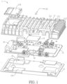
- FIG. 1 is an exploded view of an automotive electronic device according to an embodiment
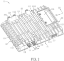
- FIG. 2 is a perspective view of the heatsink casing of FIG. 1
- FIG. 3A is a sectional view of the automotive electronic device according to the embodiment.
- the automotive electronic device 1 includes: a heatsink casing 11, a circuit board 12, and a bottom cover 13.
- the heatsink casing 11 is an aluminum die-casting casing
- the bottom cover 13 is an aluminum stamping casing or an aluminum die-casting casing.
- the automotive electronic device 1 can be, for example, a communication device, a computing device, or the like.
- the automotive electronic device 1 can be installed at a proper place inside the vehicle such as the place under the car seat, in the trunk, under the driving dashboard, or the likes.
- the circuit board 12 is installed on the bottom cover 13.
- the circuit board 12 can be a printed circuit board, a flexible circuit board, or the like.
- the circuit board 12 can be configured with one or more component units 14 such as the battery, active element, passive element and the likes (e.g. chips, antennas, resistors, capacitors, inductors, or the likes).
- the heat of the circuit board 12 and the component units can be dissipated to outside through the heatsink casing 11 and/or the bottom cover 13.
- the upper limit of the tolerable operating temperature is about 115°C. In the general vehicle conditions, the temperature of the chip will be about 10°C higher than the environment. If the vehicle temperature reaches 95°C, the temperature of the chip will be at least 95°C or more, or even at least 105°C or more, and the temperature of the heatsink casing 11 will be at least 95°C or more.
- the heatsink casing 11 is assembled with the bottom cover 13 and covers the circuit board 12 between the heatsink casing 11 and the bottom cover 13.
- the heatsink casing 11 and the bottom cover 13 can be assembled to form a closed space for accommodating the circuit board 12.
- This configuration can provide the protections (e.g. dustproof and waterproof) to the components inside the automotive electronic device such as the circuit board 12 or the component units.
- the shapes of the heatsink casing 11 and the circuit board 12 are rectangles.
- the long sides of the heatsink casing 11 and the circuit board 12 are arranged along a first direction D1
- the short sides of the heatsink casing 11 and the circuit board 12 are arranged along a second direction D2.
- the first direction D1 can be perpendicular to the second direction D2.
- the heatsink casing 11 may have a different shape, and the shape of the heatsink casing 11 depends on the shape of the circuit board 12.
- the heatsink casing 11 comprises an outer surface 111, a plurality of long fins 112, and a plurality of side fins 113.
- the long fins 112 are arranged on the outer surface 111 along the first direction D1, and two adjacent ones of the long fins 112 have a distance G1, which is at least greater than 8 mm.
- the main axis of each long fin 112 is arranged along the second direction D2 and is parallel to the short sides of the heatsink casing 11.
- the long fins 112 can be perpendicular to the outer surface 111.
- the side fins 113 are arranged on an edge of the outer surface 111 along the second direction D2 and connected to one of the long fins 112.
- the main axis of each side fin 113 is disposed along the first direction D1.
- the side fins 113 can be perpendicular to the outer surface 111.
- the side fins 113 are parallel to a gravity direction D3. That is, the normal direction of the outer surface 111 can be parallel to the gravity direction D3.
- the outer surface 111 comprises a plurality of regions 1111 and 1112 with different heights.
- the region 1112 is lower than the region 1111 so as to form a concave portion, which can allow the heatsink casing 11 to be closer to the heat source.
- the regions 1111 and 1112 are individually disposed between two adjacent ones of the long fins 112 so as to form a groove 117 with different depths or multiple grooves individually having different depths for providing different heat convection effects.
- the outer surface 111 and the long fins 112 with different heights can also form the grooves with different depths for providing different heat convection effects.
- the grooves 117 with different depths can be formed by configuring the regions 1111 and 1112 with different heights and/or the long fins 112 with different heights.
- the regions with different depths can be applied to the heat sources with different heat levels or different structural shapes.
- the part of the outer surface 111 which is right underneath the processor 141 of the circuit board 12, has a lower portion so as to form a concave portion.
- the concave portion has a thicker casing thickness, so that the heat of the processor 141 can be dissipated through the right-above groove.
- the processor 141 can be replaced by any of other electronic components (e.g. a communication module 142).
- the automotive electronic device 1 comprises a plurality of terminal joints 191 and 192
- the heatsink casing 11 comprises a plurality of joint covers 114 and 115, which are disposed over the terminal joints 191 and 192.
- a part of each of the terminal joints 191 and 192 is disposed inside the joint cover 114 or 115, and the other part thereof is protruded from the corresponding joint cover 114 or 115.
- the terminal joint 191 and the joint cover 114 are disposed at one side S1 of the heatsink casing 11, and the terminal joint 192 and the joint cover 115 are disposed at the other side S2 of the heatsink casing 11.
- the joint covers 114 and 115 are not higher than the long fins 112.
- the joint covers 114 and 115 substantially have the same height as the long fins 112.
- two long fins 1121, 1122 and the joint covers 114, 115 surround four sides of a groove 118 to enclose the groove 118, so that the air is forbidden to flow directly into the groove 118 through the four sides of the groove 118.
- the increased width of the groove 118 is configured to help a relatively cold air above the groove 118 to enter the groove 118 to induce a heat convection.
- One side of the groove 119 is not surrounded, and the residual three sides of the groove 119 are surrounded by two long fins 112 and one joint cover 114.
- This configuration can improve the problem that the air cannot flow into the groove 119 easily.
- the increased width of the groove 119 is configured to help a relatively cold air above the groove 119 to enter the groove 119 to induce a heat convection.
- the wire length on the circuit board between the processor chip and the terminal joint is as short as possible. Accordingly, the processor chip is disposed around the terminal joint. This design can overcome the poor heat dissipating issue caused by the middle parts of the terminal joints 191 and 192 and the joint covers 114 and 115, which may interfere the heat convection.
- the automotive electronic device 1 further comprises a battery 18.
- the battery 18 and the side fins 113 are disposed at two opposite sides S3 and S4 of the automotive electronic device 1, respectively.
- the battery 18 is disposed at the side S4 for preventing the influence of heat dissipation.
- the heatsink casing 11 comprises a battery cover 116, which covers the battery 18.
- the battery cover 116 comprises a recess portion 1161, and the recess portion 1161 covers above the battery 18 and contacts the battery 18 through a heat conductive element for dissipating a heat of the battery 18.
- the long fins 112 may have different lengths. For example, the long fin 1123 located next to the battery cover 116 is shorter.
- FIGS. 4 and 5 are schematic diagrams showing the airflow field of the automotive electronic device according to the embodiment
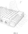
- FIG. 6 is a schematic diagram showing the airflow field of the side heat convection of the automotive electronic device according to the embodiment.
- the distance G1 between two adjacent long fins 112 is greater than 8 mm, which is obviously larger than the intervals (3 mm) of the fins of the conventional heatsink manufactured based on the process limit and the close arrangement rule. Since the distance of this disclosure is wide enough, more air can be carried to flow downwardly to supplement the original space of the hot air after the hot air rises between the long fins 112, thereby enhancing the heat convection efficiency. Compared with the conventional design (the interval of 3 mm between the fins), this disclosure can provide a better convection effect and increase the airflow circulation under the condition of maintaining or sacrificing some fins within the same surface area.
- the long fins 112 and the short sides of the heatsink casing 11 are in parallel along the second direction D2, so that the length of the fins can be reduced so as to decrease the flowing distance of air after entering the interval between the long fins 112.
- This configuration can decrease the flowing resistance and the pressure loss, and increase the heat exchange coefficient so as to increase the heat dissipating effect.
- the side fins 113 can be perpendicular to the long fins 112, and the surfaces of the side fins 113 are parallel to the gravity direction.
- This configuration can utilize the hot air buoyancy to induce the heat convection on the outer surface 111.
- the total airflow amount of the natural convection can be efficiently increased, thereby effectively utilizing the heat convection generated by the hot air buoyancy.
- the electronic device 1 further comprises a component unit 14 and a heat conductive element 15.
- the component unit 14 is disposed on the circuit board 12, and a gap G2 between the component unit 14 and the heatsink casing 11 is less than 0.5 mm.
- the heat conductive element 15 is filled in the gap G2, and a thickness of the heat conductive element 15 in the gap G2 is less than 0.5 mm.
- the heat conductive element 15 can be a heat conductive paste, a heat conductive pad, or a heat conductive putty.
- the heat conductive paste is a heat conductive AB glue.
- the component unit 14 is an active element, a passive element, or the like, such as a chip, an antenna, a resistor, a capacitor, or an inductor.
- the bottom cover 13 further comprises a protruding platform 131, which protrudes from the bottom cover 13 towards the heatsink casing 11.
- a gap G3 between the circuit board 12 and the protruding platform 131 is less than 2 mm
- a heat conductive element 16 is filled in the gap G3, and a thickness of the heat conductive element 16 in the gap G3 is less than 0.2 mm.
- the heat conductive element 16 can be a heat conductive paste, a heat conductive pad, or a heat conductive putty.
- the heat conductive paste is a heat conductive AB glue.
- the protruding platform 132 is disposed right underneath the communication module 142 of the circuit board 12 and is located adjacent to the lower surface of the circuit board 12.
- This configuration is benefit for dissipating the heat of the communication module 142 through the protruding platform 132.
- the communication module can be replaced by any of other heat sources, such as a processor.
- a heat conductive element can be provided between the protruding platform 132 and the circuit board 12.
- the electronic device may further comprise a heat conductive medium 17.
- the heat conductive medium 17 can be disposed on the upper surface of the circuit board 12 and contact the heatsink casing 11. Alternatively, the heat conductive medium 17 can be disposed on the lower surface of the circuit board 12 and contact the bottom cover 13.
- the heat conductive medium 17 is a heat conductive AB glue.
- the thickness of the heat conductive medium 17 can be less than 0.5 mm or, preferably, less than 0.2 mm.
- the heat conductive medium 17 may encapsulate some components.
- the gap between the component (unit) and the heatsink casing can be filled by the heat conductive element or medium for decreasing the thermal resistance.
- the thermal resistance of thermal conduction is directly proportional to the thickness of the heat conductive medium and inversely proportional to the thermal conductivity coefficient. Therefore, reducing the thickness of the heat conductive medium to less than 0.5 mm can greatly reduce the thermal resistance of thermal conduction.
- the gap G2 between the component unit 14 and the heatsink casing 11 is less than 0.5 mm. Therefore, the thickness of the heat conductive element 15 in the gap G2 is less than 0.5 mm, which can greatly reduce the thermal resistance of thermal conduction.
- the thickness of the heat conductive element 16 in the gap G3 is less than 0.2 mm, and the thickness of the heat conductive medium 17 can be less than 0.5 mm, or even less than 0.2 mm, which can greatly reduce the thermal resistance of thermal conduction.
- the heat conductive medium also provides the function of absorbing assembly tolerances, so a thicker heat conductive medium with the compressible property is used.
- the thickness of the thermal conductive medium is usually more than 2 mm.
- a heat conductive medium with a high thermal conductivity coefficient must be used.
- the heat conductive medium with a high thermal conductivity coefficient may lead to the increase of hardness and decrease of compression. Therefore, the heat conductive medium must be thicker, which leads to a vicious cycle of design. In contrast, the automotive electronic device of this disclosure can avoid the above-mentioned vicious cycle.
- the distance between two adjacent long fins is at least greater than 8 mm, which is obviously larger than the intervals (3 mm) of the fins of the conventional heatsink manufactured based on the process limit and the close arrangement rule. Since the distance of this disclosure is wide enough, more air can be carried to flow downwardly to supplement the original space of the hot air after the hot air rises between the fins. Compared with the conventional design (the interval of 3 mm between the fins), this disclosure can provide a better convection effect and increase the airflow circulation under the condition of maintaining or sacrificing some fins within the same surface area. Accordingly, the automotive electronic device of this disclosure is durable in the automotive environment of at least 95°C.
- the long fins and the short sides of the heatsink casing are in parallel along the second direction, so that the length of the fins can be reduced so as to decrease the flowing distance of air after entering the interval between the fins.
- This configuration can decrease the flowing resistance and the pressure loss, and increase the heat exchange coefficient.
- the side fins are perpendicular to the long fins, and the surfaces of the side fins are parallel to the gravity direction. Thus, the heat convection generated by the hot air buoyancy can be effectively utilized.
- the gap between the component unit and the heatsink casing is less than 0.5 mm, the heat conductive element is filled in the gap, and the thickness of the heat conductive element in the gap is less than 0.5 mm.
- This configuration can sufficiently decrease the heat transfer resistance. Accordingly, the automotive electronic device of this disclosure can be durable in the automotive environment of at least 95°C, and the additional fan is unnecessary. In this disclosure, only the natural convection is enough for dissipating the heat, thereby maintaining the stable operation of the electronic components inside the device.
Landscapes
- Engineering & Computer Science (AREA)
- Microelectronics & Electronic Packaging (AREA)
- Physics & Mathematics (AREA)
- Thermal Sciences (AREA)
- Cooling Or The Like Of Electrical Apparatus (AREA)
Claims (6)
- Eine elektronische Kraftfahrzeugvorrichtung (1), die in einer Kraftfahrzeugumgebung von mindestens 95 °C haltbar ist, wobei dieselbe folgende Merkmale aufweist:eine Bodenabdeckung (13);eine Schaltungsplatine (12), die auf der Bodenabdeckung installiert ist; undein Wärmesenkengehäuse (11), das mit der Bodenabdeckung zusammengebaut ist und die Schaltungsplatine zwischen dem Wärmesenkengehäuse und der Bodenabdeckung abdeckt, wobei das Wärmesenkengehäuse folgende Merkmale aufweist:eine äußere Oberfläche (111),eine Mehrzahl von langen Rippen (112), die auf der äußeren Oberfläche entlang einer ersten Richtung angeordnet sind, wobei zwei benachbarte lange Rippen einen Abstand von mindestens mehr als 8 mm aufweisen, undeine Mehrzahl von Seitenrippen (113), die auf einer Kante der äußeren Oberfläche entlang einer zweiten Richtung angeordnet sind und mit einer der langen Rippen verbunden sind, wobei die erste Richtung senkrecht zu der zweiten Richtung ist, wobei Hauptachsen der langen Rippen entlang der zweiten Richtung angeordnet sind, wobei Hauptachsen der Seitenrippen entlang der ersten Richtung angeordnet sind, und wobei das Wärmesenkengehäuse und die Bodenabdeckung zusammengebaut sind, um einen geschlossenen Raum zum Aufnehmen der Schaltungsplatine zu bilden, um der Schaltungsplatine Staub- und Wasserdichtigkeit bereitzustellen, wobei die äußere Oberfläche eine Mehrzahl von Bereichen (1111, 1112) mit unterschiedlichen Höhen aufweist, wobei die Bereiche einzeln zwischen zwei benachbarten der langen Rippen angeordnet sind, um Rillen (117) mit unterschiedlichen Tiefen zum Bereitstellen unterschiedlicher Wärmekonvektionseffekte zu bilden, wobei die Seitenrippen senkrecht zu den langen Rippen und der äußeren Oberfläche sind, wobei die Bodenabdeckung ferner eine vorstehende Plattform (131, 132) und ein wärmeleitendes Element (16) aufweist, wobei die vorstehende Plattform direkt unter einem Kommunikationsmodul (142) oder einem Prozessor (141) der Schaltungsplatine angeordnet ist, wobei ein Spalt (G3) zwischen der Schaltungsplatine und der vorstehenden Plattform konfiguriert ist, wobei das wärmeleitende Element in den Spalt gefüllt ist;wobei das Wärmesenkengehäuse ein Aluminiumdruckgussgehäuse ist und die Bodenabdeckung ein Aluminiumstanzgehäuse oder ein Aluminiumdruckgussgehäuse ist;wobei die elektronische Kraftfahrzeugvorrichtung eine Batterie (18) aufweist, wobei das Wärmesenkengehäuse eine Batterieabdeckung (116) aufweist, wobei die Batterie und die Seitenrippen an zwei gegenüberliegenden Seiten der elektronischen Kraftfahrzeugvorrichtung angeordnet sind, wobei die Batterieabdeckung einen Aussparungsabschnitt (1161) aufweist und wobei der Aussparungsabschnitt über der Batterie abdeckt und die Batterie durch ein wärmeleitendes Element zum Ableiten einer Wärme der Batterie kontaktiert; undwobei die elektronische Kraftfahrzeugvorrichtung eine Mehrzahl von Anschlussverbindungen (191, 192) aufweist, die einzeln an Seiten des Wärmesenkengehäuses angeordnet sind, wobei das Wärmesenkengehäuse eine Mehrzahl von Verbindungsabdeckungen (114, 115) aufweist, die über den Anschlussverbindungen angeordnet sind, wobei ein Teil jeder der Anschlussverbindungen innerhalb einer entsprechenden der Verbindungsabdeckungen angeordnet ist, wobei der andere Teil jeder der Anschlussverbindungen von der entsprechenden der Verbindungsabdeckungen vorsteht, wobei die Verbindungsabdeckungen im Wesentlichen die gleiche Höhe wie die langen Rippen aufweisen, und wobei in einer Ansicht von einer Oberseite des Wärmesenkengehäuses zwei der langen Rippen und die Verbindungsabdeckungen vier Seiten einer Rille umgeben, um die Rille zu umschließen.
- Die elektronische Vorrichtung gemäß Anspruch 1, wobei ein unterer Teil der äußeren Oberfläche mit einem konkaven Abschnitt ausgebildet ist, wobei der konkave Abschnitt eine dickere Gehäusedicke aufweist und wobei der konkave Abschnitt direkt über einem Kommunikationsmodul oder einem Prozessor der Schaltungsplatine angeordnet ist.
- Die elektronische Vorrichtung gemäß Anspruch 1, die ferner folgende Merkmale aufweist:eine Komponenteneinheit (14), die auf der Schaltungsplatine angeordnet ist, wobei ein Spalt (G2) zwischen der Komponenteneinheit und dem Wärmesenkengehäuse weniger als 0,5 mm beträgt; undein wärmeleitendes Element (15), das in den Spalt gefüllt ist, wobei eine Dicke des wärmeleitenden Elements in dem Spalt weniger als 0,5 mm beträgt.
- Die elektronische Vorrichtung gemäß Anspruch 1, wobei
ein Spalt zwischen der Schaltungsplatine und der vorstehenden Plattform weniger als 2 mm beträgt und eine Dicke des wärmeleitenden Elements in dem Spalt weniger als 0,2 mm beträgt. - Die elektronische Vorrichtung gemäß Anspruch 3 oder 4, wobei das wärmeleitende Element eine wärmeleitende Paste, eine wärmeleitende Kontaktfläche oder ein wärmeleitender Kitt ist.
- Die elektronische Vorrichtung gemäß Anspruch 1, die ferner folgendes Merkmal aufweist:
ein wärmeleitendes Medium (17), das auf der Schaltungsplatine angeordnet ist und das Wärmesenkengehäuse oder die Bodenabdeckung kontaktiert.
Applications Claiming Priority (1)
| Application Number | Priority Date | Filing Date | Title |
|---|---|---|---|
| TW109108844A TWI731622B (zh) | 2020-03-17 | 2020-03-17 | 車用電子裝置 |
Publications (2)
| Publication Number | Publication Date |
|---|---|
| EP3883353A1 EP3883353A1 (de) | 2021-09-22 |
| EP3883353B1 true EP3883353B1 (de) | 2024-09-18 |
Family
ID=74871168
Family Applications (1)
| Application Number | Title | Priority Date | Filing Date |
|---|---|---|---|
| EP21161866.5A Active EP3883353B1 (de) | 2020-03-17 | 2021-03-10 | Elektronische vorrichtung für kraftfahrzeuge |
Country Status (3)
| Country | Link |
|---|---|
| US (1) | US20210298203A1 (de) |
| EP (1) | EP3883353B1 (de) |
| TW (1) | TWI731622B (de) |
Families Citing this family (5)
| Publication number | Priority date | Publication date | Assignee | Title |
|---|---|---|---|---|
| US20220127013A1 (en) * | 2020-10-23 | 2022-04-28 | CCX Technologies | Secure avioncs wireless access point device with heat sink enclosure |
| TWI787877B (zh) | 2021-06-22 | 2022-12-21 | 啟碁科技股份有限公司 | 散熱結構 |
| US12111121B2 (en) * | 2021-11-18 | 2024-10-08 | Quanta Computer Inc. | Die-cast fin with opening and cover |
| DE112022005936T5 (de) * | 2021-12-15 | 2024-11-07 | Milwaukee Electric Tool Corporation | Batterieladegerät mit Kühl- und Dichtungskonstruktion |
| WO2024130625A1 (zh) * | 2022-12-22 | 2024-06-27 | 华为技术有限公司 | 散热装置、电子设备和车辆 |
Citations (1)
| Publication number | Priority date | Publication date | Assignee | Title |
|---|---|---|---|---|
| US5923084A (en) * | 1995-06-06 | 1999-07-13 | Seiko Epson Corporation | Semiconductor device for heat discharge |
Family Cites Families (7)
| Publication number | Priority date | Publication date | Assignee | Title |
|---|---|---|---|---|
| US5590026A (en) * | 1995-07-31 | 1996-12-31 | Borg-Warner Automotive, Inc. | Apparatus for dissipating heat from an integrated circuit |
| KR101887439B1 (ko) * | 2016-07-21 | 2018-08-10 | 현대오트론 주식회사 | 전자 제어 장치 |
| CN206210888U (zh) * | 2016-11-24 | 2017-05-31 | 绵阳力神动力电池系统有限公司 | 一种电动汽车电池系统外壳 |
| CN206370791U (zh) * | 2016-12-30 | 2017-08-01 | 武汉市深蓝动力科技有限公司 | 一种用于电动车的新型开关磁阻电机控制器总成结构 |
| CN106604620B (zh) * | 2017-01-24 | 2019-09-17 | 科华恒盛股份有限公司 | 一种包覆型散热器及一种电感高效散热结构 |
| CN210042477U (zh) * | 2019-04-08 | 2020-02-07 | 中山大洋电机股份有限公司 | 一种用于电动汽车的控制器 |
| CN110708917A (zh) * | 2019-11-20 | 2020-01-17 | 上海奉天电子股份有限公司 | 一种电源转换器及其制造方法 |
-
2020
- 2020-03-17 TW TW109108844A patent/TWI731622B/zh active
-
2021
- 2021-02-19 US US17/180,001 patent/US20210298203A1/en not_active Abandoned
- 2021-03-10 EP EP21161866.5A patent/EP3883353B1/de active Active
Patent Citations (1)
| Publication number | Priority date | Publication date | Assignee | Title |
|---|---|---|---|---|
| US5923084A (en) * | 1995-06-06 | 1999-07-13 | Seiko Epson Corporation | Semiconductor device for heat discharge |
Also Published As
| Publication number | Publication date |
|---|---|
| TWI731622B (zh) | 2021-06-21 |
| TW202137853A (zh) | 2021-10-01 |
| US20210298203A1 (en) | 2021-09-23 |
| EP3883353A1 (de) | 2021-09-22 |
Similar Documents
| Publication | Publication Date | Title |
|---|---|---|
| EP3883353A1 (de) | Elektronische vorrichtung für kraftfahrzeuge | |
| US5995370A (en) | Heat-sinking arrangement for circuit elements | |
| US6111749A (en) | Flexible cold plate having a one-piece coolant conduit and method employing same | |
| US6765285B2 (en) | Power semiconductor device with high radiating efficiency | |
| US5920457A (en) | Apparatus for cooling electronic devices using a flexible coolant conduit | |
| US5933324A (en) | Apparatus for dissipating heat from a conductive layer in a circuit board | |
| US7345885B2 (en) | Heat spreader with multiple stacked printed circuit boards | |
| US20110235278A1 (en) | Circuit module | |
| JP4892527B2 (ja) | 電子制御装置 | |
| JP2001119181A (ja) | 電子部品の冷却装置及び電子機器 | |
| US6101094A (en) | Printed circuit board with integrated cooling mechanism | |
| JP2010057345A (ja) | 電子制御装置 | |
| JP2023552884A (ja) | 電子デバイス | |
| JP2023552884A5 (de) | ||
| US7903408B1 (en) | Heat dissipation device of electronic circuit modules | |
| CN111279807B (zh) | 电子控制装置 | |
| JP6945514B2 (ja) | 電子制御装置 | |
| EP1178594B1 (de) | Elektronisches Gerät mit einem Substrat für die Schaltung | |
| US20080068797A1 (en) | Mounting assembly and electronic device with the mounting assembly | |
| JP4169561B2 (ja) | 電子制御装置 | |
| JP7661923B2 (ja) | 電子装置 | |
| JPH0680911B2 (ja) | 電子部品を搭載したプリント配線板の放熱構造 | |
| JP2006287080A (ja) | メモリモジュール | |
| JP4851154B2 (ja) | 回路基板内蔵筐体 | |
| JP2006339223A (ja) | Cpuの放熱構造 |
Legal Events
| Date | Code | Title | Description |
|---|---|---|---|
| PUAI | Public reference made under article 153(3) epc to a published international application that has entered the european phase |
Free format text: ORIGINAL CODE: 0009012 |
|
| STAA | Information on the status of an ep patent application or granted ep patent |
Free format text: STATUS: THE APPLICATION HAS BEEN PUBLISHED |
|
| AK | Designated contracting states |
Kind code of ref document: A1 Designated state(s): AL AT BE BG CH CY CZ DE DK EE ES FI FR GB GR HR HU IE IS IT LI LT LU LV MC MK MT NL NO PL PT RO RS SE SI SK SM TR |
|
| RAP3 | Party data changed (applicant data changed or rights of an application transferred) |
Owner name: ASKEY COMPUTER CORP. |
|
| STAA | Information on the status of an ep patent application or granted ep patent |
Free format text: STATUS: REQUEST FOR EXAMINATION WAS MADE |
|
| 17P | Request for examination filed |
Effective date: 20220307 |
|
| RBV | Designated contracting states (corrected) |
Designated state(s): AL AT BE BG CH CY CZ DE DK EE ES FI FR GB GR HR HU IE IS IT LI LT LU LV MC MK MT NL NO PL PT RO RS SE SI SK SM TR |
|
| STAA | Information on the status of an ep patent application or granted ep patent |
Free format text: STATUS: EXAMINATION IS IN PROGRESS |
|
| 17Q | First examination report despatched |
Effective date: 20231023 |
|
| GRAP | Despatch of communication of intention to grant a patent |
Free format text: ORIGINAL CODE: EPIDOSNIGR1 |
|
| STAA | Information on the status of an ep patent application or granted ep patent |
Free format text: STATUS: GRANT OF PATENT IS INTENDED |
|
| INTG | Intention to grant announced |
Effective date: 20240419 |
|
| GRAS | Grant fee paid |
Free format text: ORIGINAL CODE: EPIDOSNIGR3 |
|
| GRAA | (expected) grant |
Free format text: ORIGINAL CODE: 0009210 |
|
| STAA | Information on the status of an ep patent application or granted ep patent |
Free format text: STATUS: THE PATENT HAS BEEN GRANTED |
|
| P01 | Opt-out of the competence of the unified patent court (upc) registered |
Free format text: CASE NUMBER: APP_45006/2024 Effective date: 20240802 |
|
| AK | Designated contracting states |
Kind code of ref document: B1 Designated state(s): AL AT BE BG CH CY CZ DE DK EE ES FI FR GB GR HR HU IE IS IT LI LT LU LV MC MK MT NL NO PL PT RO RS SE SI SK SM TR |
|
| REG | Reference to a national code |
Ref country code: GB Ref legal event code: FG4D |
|
| REG | Reference to a national code |
Ref country code: CH Ref legal event code: EP |
|
| REG | Reference to a national code |
Ref country code: IE Ref legal event code: FG4D |
|
| REG | Reference to a national code |
Ref country code: DE Ref legal event code: R096 Ref document number: 602021018840 Country of ref document: DE |
|
| REG | Reference to a national code |
Ref country code: LT Ref legal event code: MG9D |
|
| PG25 | Lapsed in a contracting state [announced via postgrant information from national office to epo] |
Ref country code: NO Free format text: LAPSE BECAUSE OF FAILURE TO SUBMIT A TRANSLATION OF THE DESCRIPTION OR TO PAY THE FEE WITHIN THE PRESCRIBED TIME-LIMIT Effective date: 20241218 |
|
| PG25 | Lapsed in a contracting state [announced via postgrant information from national office to epo] |
Ref country code: GR Free format text: LAPSE BECAUSE OF FAILURE TO SUBMIT A TRANSLATION OF THE DESCRIPTION OR TO PAY THE FEE WITHIN THE PRESCRIBED TIME-LIMIT Effective date: 20241219 Ref country code: FI Free format text: LAPSE BECAUSE OF FAILURE TO SUBMIT A TRANSLATION OF THE DESCRIPTION OR TO PAY THE FEE WITHIN THE PRESCRIBED TIME-LIMIT Effective date: 20240918 |
|
| PG25 | Lapsed in a contracting state [announced via postgrant information from national office to epo] |
Ref country code: BG Free format text: LAPSE BECAUSE OF FAILURE TO SUBMIT A TRANSLATION OF THE DESCRIPTION OR TO PAY THE FEE WITHIN THE PRESCRIBED TIME-LIMIT Effective date: 20240918 |
|
| PG25 | Lapsed in a contracting state [announced via postgrant information from national office to epo] |
Ref country code: LV Free format text: LAPSE BECAUSE OF FAILURE TO SUBMIT A TRANSLATION OF THE DESCRIPTION OR TO PAY THE FEE WITHIN THE PRESCRIBED TIME-LIMIT Effective date: 20240918 |
|
| PG25 | Lapsed in a contracting state [announced via postgrant information from national office to epo] |
Ref country code: HR Free format text: LAPSE BECAUSE OF FAILURE TO SUBMIT A TRANSLATION OF THE DESCRIPTION OR TO PAY THE FEE WITHIN THE PRESCRIBED TIME-LIMIT Effective date: 20240918 |
|
| REG | Reference to a national code |
Ref country code: NL Ref legal event code: MP Effective date: 20240918 |
|
| PG25 | Lapsed in a contracting state [announced via postgrant information from national office to epo] |
Ref country code: RS Free format text: LAPSE BECAUSE OF FAILURE TO SUBMIT A TRANSLATION OF THE DESCRIPTION OR TO PAY THE FEE WITHIN THE PRESCRIBED TIME-LIMIT Effective date: 20241218 |
|
| PG25 | Lapsed in a contracting state [announced via postgrant information from national office to epo] |
Ref country code: RS Free format text: LAPSE BECAUSE OF FAILURE TO SUBMIT A TRANSLATION OF THE DESCRIPTION OR TO PAY THE FEE WITHIN THE PRESCRIBED TIME-LIMIT Effective date: 20241218 Ref country code: NO Free format text: LAPSE BECAUSE OF FAILURE TO SUBMIT A TRANSLATION OF THE DESCRIPTION OR TO PAY THE FEE WITHIN THE PRESCRIBED TIME-LIMIT Effective date: 20241218 Ref country code: LV Free format text: LAPSE BECAUSE OF FAILURE TO SUBMIT A TRANSLATION OF THE DESCRIPTION OR TO PAY THE FEE WITHIN THE PRESCRIBED TIME-LIMIT Effective date: 20240918 Ref country code: HR Free format text: LAPSE BECAUSE OF FAILURE TO SUBMIT A TRANSLATION OF THE DESCRIPTION OR TO PAY THE FEE WITHIN THE PRESCRIBED TIME-LIMIT Effective date: 20240918 Ref country code: GR Free format text: LAPSE BECAUSE OF FAILURE TO SUBMIT A TRANSLATION OF THE DESCRIPTION OR TO PAY THE FEE WITHIN THE PRESCRIBED TIME-LIMIT Effective date: 20241219 Ref country code: FI Free format text: LAPSE BECAUSE OF FAILURE TO SUBMIT A TRANSLATION OF THE DESCRIPTION OR TO PAY THE FEE WITHIN THE PRESCRIBED TIME-LIMIT Effective date: 20240918 Ref country code: BG Free format text: LAPSE BECAUSE OF FAILURE TO SUBMIT A TRANSLATION OF THE DESCRIPTION OR TO PAY THE FEE WITHIN THE PRESCRIBED TIME-LIMIT Effective date: 20240918 |
|
| REG | Reference to a national code |
Ref country code: AT Ref legal event code: MK05 Ref document number: 1725812 Country of ref document: AT Kind code of ref document: T Effective date: 20240918 |
|
| PG25 | Lapsed in a contracting state [announced via postgrant information from national office to epo] |
Ref country code: NL Free format text: LAPSE BECAUSE OF FAILURE TO SUBMIT A TRANSLATION OF THE DESCRIPTION OR TO PAY THE FEE WITHIN THE PRESCRIBED TIME-LIMIT Effective date: 20240918 |
|
| PG25 | Lapsed in a contracting state [announced via postgrant information from national office to epo] |
Ref country code: IS Free format text: LAPSE BECAUSE OF FAILURE TO SUBMIT A TRANSLATION OF THE DESCRIPTION OR TO PAY THE FEE WITHIN THE PRESCRIBED TIME-LIMIT Effective date: 20250118 Ref country code: PT Free format text: LAPSE BECAUSE OF FAILURE TO SUBMIT A TRANSLATION OF THE DESCRIPTION OR TO PAY THE FEE WITHIN THE PRESCRIBED TIME-LIMIT Effective date: 20250120 |
|
| PGFP | Annual fee paid to national office [announced via postgrant information from national office to epo] |
Ref country code: DE Payment date: 20250305 Year of fee payment: 5 |
|
| PG25 | Lapsed in a contracting state [announced via postgrant information from national office to epo] |
Ref country code: RO Free format text: LAPSE BECAUSE OF FAILURE TO SUBMIT A TRANSLATION OF THE DESCRIPTION OR TO PAY THE FEE WITHIN THE PRESCRIBED TIME-LIMIT Effective date: 20240918 Ref country code: SM Free format text: LAPSE BECAUSE OF FAILURE TO SUBMIT A TRANSLATION OF THE DESCRIPTION OR TO PAY THE FEE WITHIN THE PRESCRIBED TIME-LIMIT Effective date: 20240918 |
|
| PG25 | Lapsed in a contracting state [announced via postgrant information from national office to epo] |
Ref country code: ES Free format text: LAPSE BECAUSE OF FAILURE TO SUBMIT A TRANSLATION OF THE DESCRIPTION OR TO PAY THE FEE WITHIN THE PRESCRIBED TIME-LIMIT Effective date: 20240918 |
|
| PG25 | Lapsed in a contracting state [announced via postgrant information from national office to epo] |
Ref country code: EE Free format text: LAPSE BECAUSE OF FAILURE TO SUBMIT A TRANSLATION OF THE DESCRIPTION OR TO PAY THE FEE WITHIN THE PRESCRIBED TIME-LIMIT Effective date: 20240918 Ref country code: AT Free format text: LAPSE BECAUSE OF FAILURE TO SUBMIT A TRANSLATION OF THE DESCRIPTION OR TO PAY THE FEE WITHIN THE PRESCRIBED TIME-LIMIT Effective date: 20240918 |
|
| PG25 | Lapsed in a contracting state [announced via postgrant information from national office to epo] |
Ref country code: PL Free format text: LAPSE BECAUSE OF FAILURE TO SUBMIT A TRANSLATION OF THE DESCRIPTION OR TO PAY THE FEE WITHIN THE PRESCRIBED TIME-LIMIT Effective date: 20240918 Ref country code: CZ Free format text: LAPSE BECAUSE OF FAILURE TO SUBMIT A TRANSLATION OF THE DESCRIPTION OR TO PAY THE FEE WITHIN THE PRESCRIBED TIME-LIMIT Effective date: 20240918 |
|
| PGFP | Annual fee paid to national office [announced via postgrant information from national office to epo] |
Ref country code: FR Payment date: 20250326 Year of fee payment: 5 |
|
| PG25 | Lapsed in a contracting state [announced via postgrant information from national office to epo] |
Ref country code: SK Free format text: LAPSE BECAUSE OF FAILURE TO SUBMIT A TRANSLATION OF THE DESCRIPTION OR TO PAY THE FEE WITHIN THE PRESCRIBED TIME-LIMIT Effective date: 20240918 Ref country code: IT Free format text: LAPSE BECAUSE OF FAILURE TO SUBMIT A TRANSLATION OF THE DESCRIPTION OR TO PAY THE FEE WITHIN THE PRESCRIBED TIME-LIMIT Effective date: 20240918 |
|
| PGFP | Annual fee paid to national office [announced via postgrant information from national office to epo] |
Ref country code: GB Payment date: 20250322 Year of fee payment: 5 |
|
| REG | Reference to a national code |
Ref country code: DE Ref legal event code: R097 Ref document number: 602021018840 Country of ref document: DE |
|
| PG25 | Lapsed in a contracting state [announced via postgrant information from national office to epo] |
Ref country code: DK Free format text: LAPSE BECAUSE OF FAILURE TO SUBMIT A TRANSLATION OF THE DESCRIPTION OR TO PAY THE FEE WITHIN THE PRESCRIBED TIME-LIMIT Effective date: 20240918 |
|
| PLBE | No opposition filed within time limit |
Free format text: ORIGINAL CODE: 0009261 |
|
| STAA | Information on the status of an ep patent application or granted ep patent |
Free format text: STATUS: NO OPPOSITION FILED WITHIN TIME LIMIT |
|
| 26N | No opposition filed |
Effective date: 20250619 |
|
| PG25 | Lapsed in a contracting state [announced via postgrant information from national office to epo] |
Ref country code: SE Free format text: LAPSE BECAUSE OF FAILURE TO SUBMIT A TRANSLATION OF THE DESCRIPTION OR TO PAY THE FEE WITHIN THE PRESCRIBED TIME-LIMIT Effective date: 20240918 |
|
| PG25 | Lapsed in a contracting state [announced via postgrant information from national office to epo] |
Ref country code: MC Free format text: LAPSE BECAUSE OF FAILURE TO SUBMIT A TRANSLATION OF THE DESCRIPTION OR TO PAY THE FEE WITHIN THE PRESCRIBED TIME-LIMIT Effective date: 20240918 |
|
| REG | Reference to a national code |
Ref country code: CH Ref legal event code: H13 Free format text: ST27 STATUS EVENT CODE: U-0-0-H10-H13 (AS PROVIDED BY THE NATIONAL OFFICE) Effective date: 20251023 |
|
| PG25 | Lapsed in a contracting state [announced via postgrant information from national office to epo] |
Ref country code: LU Free format text: LAPSE BECAUSE OF NON-PAYMENT OF DUE FEES Effective date: 20250310 |
|
| REG | Reference to a national code |
Ref country code: BE Ref legal event code: MM Effective date: 20250331 |
|
| PG25 | Lapsed in a contracting state [announced via postgrant information from national office to epo] |
Ref country code: BE Free format text: LAPSE BECAUSE OF NON-PAYMENT OF DUE FEES Effective date: 20250331 |
|
| PG25 | Lapsed in a contracting state [announced via postgrant information from national office to epo] |
Ref country code: CH Free format text: LAPSE BECAUSE OF NON-PAYMENT OF DUE FEES Effective date: 20250331 |
|
| PG25 | Lapsed in a contracting state [announced via postgrant information from national office to epo] |
Ref country code: IE Free format text: LAPSE BECAUSE OF NON-PAYMENT OF DUE FEES Effective date: 20250310 |