EP3883130A1 - Bulk acoustic wave resonator, filter, and electronic device - Google Patents
Bulk acoustic wave resonator, filter, and electronic device Download PDFInfo
- Publication number
- EP3883130A1 EP3883130A1 EP19884110.8A EP19884110A EP3883130A1 EP 3883130 A1 EP3883130 A1 EP 3883130A1 EP 19884110 A EP19884110 A EP 19884110A EP 3883130 A1 EP3883130 A1 EP 3883130A1
- Authority
- EP
- European Patent Office
- Prior art keywords
- top electrode
- passivation layer
- resonator according
- layer
- range
- Prior art date
- Legal status (The legal status is an assumption and is not a legal conclusion. Google has not performed a legal analysis and makes no representation as to the accuracy of the status listed.)
- Pending
Links
- 239000000758 substrate Substances 0.000 claims abstract description 53
- 230000001629 suppression Effects 0.000 claims abstract description 20
- 238000002161 passivation Methods 0.000 claims description 110
- 229910052751 metal Inorganic materials 0.000 claims description 34
- 239000002184 metal Substances 0.000 claims description 34
- 239000007772 electrode material Substances 0.000 claims description 25
- 239000000725 suspension Substances 0.000 claims description 7
- VYPSYNLAJGMNEJ-UHFFFAOYSA-N silicon dioxide Inorganic materials O=[Si]=O VYPSYNLAJGMNEJ-UHFFFAOYSA-N 0.000 description 58
- 239000000377 silicon dioxide Substances 0.000 description 27
- 239000011651 chromium Substances 0.000 description 22
- QVGXLLKOCUKJST-UHFFFAOYSA-N atomic oxygen Chemical compound [O] QVGXLLKOCUKJST-UHFFFAOYSA-N 0.000 description 21
- 229910052760 oxygen Inorganic materials 0.000 description 21
- 239000001301 oxygen Substances 0.000 description 21
- 239000000463 material Substances 0.000 description 19
- 235000012239 silicon dioxide Nutrition 0.000 description 16
- VYZAMTAEIAYCRO-UHFFFAOYSA-N Chromium Chemical compound [Cr] VYZAMTAEIAYCRO-UHFFFAOYSA-N 0.000 description 11
- 229910052804 chromium Inorganic materials 0.000 description 11
- 239000006185 dispersion Substances 0.000 description 11
- 239000007769 metal material Substances 0.000 description 11
- XLYOFNOQVPJJNP-UHFFFAOYSA-N water Chemical compound O XLYOFNOQVPJJNP-UHFFFAOYSA-N 0.000 description 10
- 239000003989 dielectric material Substances 0.000 description 8
- 230000003071 parasitic effect Effects 0.000 description 8
- PMHQVHHXPFUNSP-UHFFFAOYSA-M copper(1+);methylsulfanylmethane;bromide Chemical compound Br[Cu].CSC PMHQVHHXPFUNSP-UHFFFAOYSA-M 0.000 description 7
- 229910052581 Si3N4 Inorganic materials 0.000 description 5
- HQVNEWCFYHHQES-UHFFFAOYSA-N silicon nitride Chemical compound N12[Si]34N5[Si]62N3[Si]51N64 HQVNEWCFYHHQES-UHFFFAOYSA-N 0.000 description 5
- OKTJSMMVPCPJKN-UHFFFAOYSA-N Carbon Chemical compound [C] OKTJSMMVPCPJKN-UHFFFAOYSA-N 0.000 description 4
- RTZKZFJDLAIYFH-UHFFFAOYSA-N Diethyl ether Chemical compound CCOCC RTZKZFJDLAIYFH-UHFFFAOYSA-N 0.000 description 4
- 229910052799 carbon Inorganic materials 0.000 description 4
- BASFCYQUMIYNBI-UHFFFAOYSA-N platinum Chemical compound [Pt] BASFCYQUMIYNBI-UHFFFAOYSA-N 0.000 description 3
- HBMJWWWQQXIZIP-UHFFFAOYSA-N silicon carbide Chemical compound [Si+]#[C-] HBMJWWWQQXIZIP-UHFFFAOYSA-N 0.000 description 3
- ZOKXTWBITQBERF-UHFFFAOYSA-N Molybdenum Chemical compound [Mo] ZOKXTWBITQBERF-UHFFFAOYSA-N 0.000 description 2
- 229910003481 amorphous carbon Inorganic materials 0.000 description 2
- 230000008878 coupling Effects 0.000 description 2
- 238000010168 coupling process Methods 0.000 description 2
- 238000005859 coupling reaction Methods 0.000 description 2
- 229910003460 diamond Inorganic materials 0.000 description 2
- 239000010432 diamond Substances 0.000 description 2
- 230000005284 excitation Effects 0.000 description 2
- 239000004811 fluoropolymer Substances 0.000 description 2
- 239000010931 gold Substances 0.000 description 2
- 239000011777 magnesium Substances 0.000 description 2
- 229910052750 molybdenum Inorganic materials 0.000 description 2
- 239000011733 molybdenum Substances 0.000 description 2
- TWNQGVIAIRXVLR-UHFFFAOYSA-N oxo(oxoalumanyloxy)alumane Chemical compound O=[Al]O[Al]=O TWNQGVIAIRXVLR-UHFFFAOYSA-N 0.000 description 2
- 229920003209 poly(hydridosilsesquioxane) Polymers 0.000 description 2
- 229920000052 poly(p-xylylene) Polymers 0.000 description 2
- 229920000412 polyarylene Polymers 0.000 description 2
- 239000010453 quartz Substances 0.000 description 2
- 229910010271 silicon carbide Inorganic materials 0.000 description 2
- 229910052814 silicon oxide Inorganic materials 0.000 description 2
- 239000010936 titanium Substances 0.000 description 2
- WFKWXMTUELFFGS-UHFFFAOYSA-N tungsten Chemical compound [W] WFKWXMTUELFFGS-UHFFFAOYSA-N 0.000 description 2
- 229910052721 tungsten Inorganic materials 0.000 description 2
- 239000010937 tungsten Substances 0.000 description 2
- YGVYHUGLHHFGNN-UHFFFAOYSA-N (2-phenylcyclobuten-1-yl)benzene Chemical compound C1CC(C=2C=CC=CC=2)=C1C1=CC=CC=C1 YGVYHUGLHHFGNN-UHFFFAOYSA-N 0.000 description 1
- PIGFYZPCRLYGLF-UHFFFAOYSA-N Aluminum nitride Chemical compound [Al]#N PIGFYZPCRLYGLF-UHFFFAOYSA-N 0.000 description 1
- JBRZTFJDHDCESZ-UHFFFAOYSA-N AsGa Chemical compound [As]#[Ga] JBRZTFJDHDCESZ-UHFFFAOYSA-N 0.000 description 1
- FYYHWMGAXLPEAU-UHFFFAOYSA-N Magnesium Chemical compound [Mg] FYYHWMGAXLPEAU-UHFFFAOYSA-N 0.000 description 1
- 229920000265 Polyparaphenylene Polymers 0.000 description 1
- KJTLSVCANCCWHF-UHFFFAOYSA-N Ruthenium Chemical compound [Ru] KJTLSVCANCCWHF-UHFFFAOYSA-N 0.000 description 1
- XUIMIQQOPSSXEZ-UHFFFAOYSA-N Silicon Chemical compound [Si] XUIMIQQOPSSXEZ-UHFFFAOYSA-N 0.000 description 1
- RTAQQCXQSZGOHL-UHFFFAOYSA-N Titanium Chemical compound [Ti] RTAQQCXQSZGOHL-UHFFFAOYSA-N 0.000 description 1
- XLOMVQKBTHCTTD-UHFFFAOYSA-N Zinc monoxide Chemical compound [Zn]=O XLOMVQKBTHCTTD-UHFFFAOYSA-N 0.000 description 1
- 229910052782 aluminium Inorganic materials 0.000 description 1
- XAGFODPZIPBFFR-UHFFFAOYSA-N aluminium Chemical compound [Al] XAGFODPZIPBFFR-UHFFFAOYSA-N 0.000 description 1
- 230000015572 biosynthetic process Effects 0.000 description 1
- 238000004891 communication Methods 0.000 description 1
- 239000002131 composite material Substances 0.000 description 1
- 239000013078 crystal Substances 0.000 description 1
- 230000006866 deterioration Effects 0.000 description 1
- 238000005516 engineering process Methods 0.000 description 1
- 238000001914 filtration Methods 0.000 description 1
- -1 fluorinated silicon dioxide (fluorinated silicon dioxide Chemical class 0.000 description 1
- PCHJSUWPFVWCPO-UHFFFAOYSA-N gold Chemical compound [Au] PCHJSUWPFVWCPO-UHFFFAOYSA-N 0.000 description 1
- 229910052737 gold Inorganic materials 0.000 description 1
- 239000012535 impurity Substances 0.000 description 1
- 238000003780 insertion Methods 0.000 description 1
- 230000037431 insertion Effects 0.000 description 1
- 230000010354 integration Effects 0.000 description 1
- 239000013067 intermediate product Substances 0.000 description 1
- 238000002955 isolation Methods 0.000 description 1
- 229910052749 magnesium Inorganic materials 0.000 description 1
- 230000010358 mechanical oscillation Effects 0.000 description 1
- 229910021421 monocrystalline silicon Inorganic materials 0.000 description 1
- 230000024241 parasitism Effects 0.000 description 1
- 230000035515 penetration Effects 0.000 description 1
- 229910052697 platinum Inorganic materials 0.000 description 1
- 239000000047 product Substances 0.000 description 1
- 229910052707 ruthenium Inorganic materials 0.000 description 1
- 229910052594 sapphire Inorganic materials 0.000 description 1
- 239000010980 sapphire Substances 0.000 description 1
- 229910052706 scandium Inorganic materials 0.000 description 1
- SIXSYDAISGFNSX-UHFFFAOYSA-N scandium atom Chemical compound [Sc] SIXSYDAISGFNSX-UHFFFAOYSA-N 0.000 description 1
- 239000004065 semiconductor Substances 0.000 description 1
- 229910052710 silicon Inorganic materials 0.000 description 1
- 239000010703 silicon Substances 0.000 description 1
- 238000010897 surface acoustic wave method Methods 0.000 description 1
- 229910052719 titanium Inorganic materials 0.000 description 1
- 230000007704 transition Effects 0.000 description 1
Images







Classifications
-
- H—ELECTRICITY
- H03—ELECTRONIC CIRCUITRY
- H03H—IMPEDANCE NETWORKS, e.g. RESONANT CIRCUITS; RESONATORS
- H03H3/00—Apparatus or processes specially adapted for the manufacture of impedance networks, resonating circuits, resonators
- H03H3/007—Apparatus or processes specially adapted for the manufacture of impedance networks, resonating circuits, resonators for the manufacture of electromechanical resonators or networks
- H03H3/02—Apparatus or processes specially adapted for the manufacture of impedance networks, resonating circuits, resonators for the manufacture of electromechanical resonators or networks for the manufacture of piezoelectric or electrostrictive resonators or networks
-
- H—ELECTRICITY
- H03—ELECTRONIC CIRCUITRY
- H03H—IMPEDANCE NETWORKS, e.g. RESONANT CIRCUITS; RESONATORS
- H03H9/00—Networks comprising electromechanical or electro-acoustic elements; Electromechanical resonators
- H03H9/02—Details
- H03H9/02007—Details of bulk acoustic wave devices
- H03H9/02086—Means for compensation or elimination of undesirable effects
- H03H9/02118—Means for compensation or elimination of undesirable effects of lateral leakage between adjacent resonators
-
- H—ELECTRICITY
- H03—ELECTRONIC CIRCUITRY
- H03H—IMPEDANCE NETWORKS, e.g. RESONANT CIRCUITS; RESONATORS
- H03H9/00—Networks comprising electromechanical or electro-acoustic elements; Electromechanical resonators
- H03H9/02—Details
- H03H9/02007—Details of bulk acoustic wave devices
- H03H9/02015—Characteristics of piezoelectric layers, e.g. cutting angles
-
- H—ELECTRICITY
- H03—ELECTRONIC CIRCUITRY
- H03H—IMPEDANCE NETWORKS, e.g. RESONANT CIRCUITS; RESONATORS
- H03H9/00—Networks comprising electromechanical or electro-acoustic elements; Electromechanical resonators
- H03H9/02—Details
- H03H9/02007—Details of bulk acoustic wave devices
- H03H9/02157—Dimensional parameters, e.g. ratio between two dimension parameters, length, width or thickness
-
- H—ELECTRICITY
- H03—ELECTRONIC CIRCUITRY
- H03H—IMPEDANCE NETWORKS, e.g. RESONANT CIRCUITS; RESONATORS
- H03H9/00—Networks comprising electromechanical or electro-acoustic elements; Electromechanical resonators
- H03H9/02—Details
- H03H9/125—Driving means, e.g. electrodes, coils
- H03H9/13—Driving means, e.g. electrodes, coils for networks consisting of piezoelectric or electrostrictive materials
- H03H9/131—Driving means, e.g. electrodes, coils for networks consisting of piezoelectric or electrostrictive materials consisting of a multilayered structure
-
- H—ELECTRICITY
- H03—ELECTRONIC CIRCUITRY
- H03H—IMPEDANCE NETWORKS, e.g. RESONANT CIRCUITS; RESONATORS
- H03H9/00—Networks comprising electromechanical or electro-acoustic elements; Electromechanical resonators
- H03H9/02—Details
- H03H9/125—Driving means, e.g. electrodes, coils
- H03H9/13—Driving means, e.g. electrodes, coils for networks consisting of piezoelectric or electrostrictive materials
- H03H9/132—Driving means, e.g. electrodes, coils for networks consisting of piezoelectric or electrostrictive materials characterized by a particular shape
-
- H—ELECTRICITY
- H03—ELECTRONIC CIRCUITRY
- H03H—IMPEDANCE NETWORKS, e.g. RESONANT CIRCUITS; RESONATORS
- H03H9/00—Networks comprising electromechanical or electro-acoustic elements; Electromechanical resonators
- H03H9/15—Constructional features of resonators consisting of piezoelectric or electrostrictive material
- H03H9/17—Constructional features of resonators consisting of piezoelectric or electrostrictive material having a single resonator
- H03H9/171—Constructional features of resonators consisting of piezoelectric or electrostrictive material having a single resonator implemented with thin-film techniques, i.e. of the film bulk acoustic resonator [FBAR] type
-
- H—ELECTRICITY
- H03—ELECTRONIC CIRCUITRY
- H03H—IMPEDANCE NETWORKS, e.g. RESONANT CIRCUITS; RESONATORS
- H03H9/00—Networks comprising electromechanical or electro-acoustic elements; Electromechanical resonators
- H03H9/15—Constructional features of resonators consisting of piezoelectric or electrostrictive material
- H03H9/17—Constructional features of resonators consisting of piezoelectric or electrostrictive material having a single resonator
- H03H9/171—Constructional features of resonators consisting of piezoelectric or electrostrictive material having a single resonator implemented with thin-film techniques, i.e. of the film bulk acoustic resonator [FBAR] type
- H03H9/172—Means for mounting on a substrate, i.e. means constituting the material interface confining the waves to a volume
- H03H9/173—Air-gaps
-
- H—ELECTRICITY
- H03—ELECTRONIC CIRCUITRY
- H03H—IMPEDANCE NETWORKS, e.g. RESONANT CIRCUITS; RESONATORS
- H03H9/00—Networks comprising electromechanical or electro-acoustic elements; Electromechanical resonators
- H03H9/46—Filters
- H03H9/54—Filters comprising resonators of piezoelectric or electrostrictive material
-
- H—ELECTRICITY
- H03—ELECTRONIC CIRCUITRY
- H03H—IMPEDANCE NETWORKS, e.g. RESONANT CIRCUITS; RESONATORS
- H03H3/00—Apparatus or processes specially adapted for the manufacture of impedance networks, resonating circuits, resonators
- H03H3/007—Apparatus or processes specially adapted for the manufacture of impedance networks, resonating circuits, resonators for the manufacture of electromechanical resonators or networks
- H03H3/02—Apparatus or processes specially adapted for the manufacture of impedance networks, resonating circuits, resonators for the manufacture of electromechanical resonators or networks for the manufacture of piezoelectric or electrostrictive resonators or networks
- H03H2003/023—Apparatus or processes specially adapted for the manufacture of impedance networks, resonating circuits, resonators for the manufacture of electromechanical resonators or networks for the manufacture of piezoelectric or electrostrictive resonators or networks the resonators or networks being of the membrane type
-
- H—ELECTRICITY
- H03—ELECTRONIC CIRCUITRY
- H03H—IMPEDANCE NETWORKS, e.g. RESONANT CIRCUITS; RESONATORS
- H03H9/00—Networks comprising electromechanical or electro-acoustic elements; Electromechanical resonators
- H03H9/02—Details
- H03H2009/02165—Tuning
- H03H2009/02173—Tuning of film bulk acoustic resonators [FBAR]
Definitions
- Embodiments of the present invention relate to the field of semiconductors, in particular to a bulk acoustic wave resonator, a filter having the resonator, and an electronic device having the filter.
- a film bulk wave resonator made by the longitudinal resonance of a piezoelectric film in the thickness direction has become a feasible alternative to surface acoustic wave devices and quartz crystal resonators in terms of machine communication and high-speed serial data applications.
- a radio frequency front end bulk wave filter/duplexer provides superior filtering characteristics, such as low insertion loss, steep transition band, higher power capacity, and stronger electrostatic discharge (ESD) resistance.
- ESD electrostatic discharge
- a high-frequency film bulk wave oscillator with ultra-low frequency temperature drift has low phase noise, low power consumption and a large bandwidth modulation range.
- these miniature film resonators use CMOS-compatible processing technology on silicon substrates, which can reduce the unit cost and facilitate the final integration with CMOS circuits.
- the bulk wave resonator includes an acoustic mirror, two electrodes, and a piezoelectric material layer called piezoelectric excitation between the two electrodes.
- a bottom electrode and a top electrode are also called excitation electrodes, and their function is to cause mechanical oscillation of each layer of the resonator.
- An acoustic mirror forms acoustic isolation between the bulk wave resonator and the substrate to prevent acoustic waves from being conducted to the outside of the resonator to cause energy loss.
- the example 1200A in Fig. 12A is a top view of a traditional bulk acoustic wave resonator.
- the acoustic mirror 1201 is composed of an air cavity on the substrate, and its function is to approximately convert the acoustic impedance of the substrate into the acoustic impedance of air.
- Most of the bottom electrode (not shown here) should be located on the inner side of the boundary of the acoustic mirror 1201.
- the bottom electrode is covered with a piezoelectric film 1203, and the boundary of the piezoelectric film is located on the outer side of the boundary of the acoustic mirror.
- the piezoelectric layer is covered with a top electrode 1204, and the top electrode has an extended end 1205 at the same time.
- the example 1201A in Fig. 12B is a schematic section view of the example 1200A at AA'.
- the structure includes a substrate 1210, an acoustic mirror 1211, a bottom electrode 1212, a piezoelectric layer 1213 and a top electrode 1214.
- the energy of an alternating electrical signal applied to the top electrode and the bottom electrode is only converted into the acoustic energy of a longitudinal vibration mode (usually called a piston mode) of the piezoelectric layer.
- a longitudinal vibration mode usually called a piston mode
- acoustic waves in a transverse vibration mode are also generated, the existence of the waves in the transverse vibration mode will weaken the energy of the acoustic waves in the piston mode, thereby resulting in serious deterioration in the key performance parameters of the device such as quality factor (Q) and effective electromechanical coupling factor ( K 2 t,eff ) .
- the filter constructed by the bulk acoustic wave resonator also generates noise on a filter frequency characteristic curve, thereby reducing the performance of the filter system.
- the transverse mode is parasitic in the entire space formed by the upper bottom electrode and the piezoelectric layer. Especially when the geometrical shape of the cross section of the film layer has parallel sides in pairs, the transverse mode will be enhanced because of the formation of standing waves.
- the top electrode has a rectangular cross section structure, the structure is suitable for acoustic waves in the parasitic mode to form stable standing waves therein, so that the acoustic waves in the parasitic mode occupy considerable energy, which seriously affects the performance of the resonator. Therefore, the structure of the top electrode structure needs to be improved to improve the performance of the resonator.
- the present invention is proposed.
- a bulk acoustic wave resonator including: a substrate; an acoustic mirror; a bottom electrode arranged above the substrate; a top electrode opposed to the bottom electrode; and a piezoelectric layer arranged above the bottom electrode and between the bottom electrode and the top electrode, wherein at least one of the two ends of the top electrode is provided with a transverse mode vibration suppression structure.
- the suppression structure includes a non-parallel structure of upper and lower surfaces arranged on at least one of the two ends of the top electrode.
- At least a part of at least one of the upper and lower surfaces of at least one end of the top electrode is an inclined surface.
- the angle formed by the inclined surface and the surface of the substrate is 15-75 degrees.
- the length of the inclined surface in the horizontal direction ranges from 0.02 ⁇ m to 3 ⁇ m.
- At least one of the upper and lower surfaces of at least one end of the top electrode includes: a vertical extension surface and/or a horizontal extension surface; and the inclined surface.
- the suppression structure includes a non-vertical surface that is arranged at the end face of at least one end of the top electrode and is different from a vertical surface, wherein the vertical surface is perpendicular to the surface of the substrate.
- the non-vertical surface has a shape of a concave surface or a convex surface.
- the above-mentioned resonator further includes a passivation layer arranged on the top electrode. Further, the thickness of the passivation layer is 0.01 ⁇ m to 0. 1um.
- the above-mentioned resonator further includes a metal electrode material layer and a passivation layer, which are sequentially arranged on the top electrode. Further, the thickness of the metal electrode material layer is 0.04 ⁇ m to 0.24 ⁇ m.
- At least one end part of the top electrode comprises a suspension wing structure, and the suspension wing structure includes the suppression structure.
- the two ends of the top electrode are axisymmetric structures to each other.
- the resonator further includes a passivation layer, and the passivation layer is disposed to cover the top electrode, wherein: at least one end of the passivation layer extends beyond the corresponding end of the top electrode; and the end of the passivation layer extending beyond the corresponding end of the top electrode is provided with the suppression structure.
- the suppression structure includes a non-parallel structure of upper and lower surfaces of the passivation layer; and/or the suppression structure includes a non-vertical structure that is arranged at the end face of at least one end of the passivation layer and is different from the vertical surface, wherein the vertical surface is perpendicular to the surface of the substrate.
- At least one end part of the top electrode comprises a suspension wing structure.
- the two ends of the passivation layer extend beyond the corresponding end parts of the top electrode and are axisymmetric structures to each other.
- the distance of the end part of the passivation layer extending beyond the top electrode is 0.1 ⁇ m to 3 ⁇ m.
- the thickness of the passivation layer is 0.04 ⁇ m to 0.24 ⁇ m.
- the embodiment of the present invention further relates to a filter, including the above-mentioned bulk acoustic wave resonator.
- the embodiment of the present invention further relates to an electronic device, including the above-mentioned filter.
- a detail structure is arranged at the end part of a top electrode of a bulk acoustic wave resonator in the present invention, for example, this kind of detail structure can effectively eliminate or reduce the parallelism of the opposite sides, and destroy the condition or geometric structure of the transverse acoustic vibration mode to form the standing waves in the top electrode, thereby effectively suppressing the parasitic transverse mode vibration in the top electrode, so that more transverse mode vibration energy can be converted into useful piston mode vibration energy, and the Q value of the resonator is improved as a result.
- a dispersion curve near the resonance frequency is optimized by introducing different materials to from a composite top electrode, and at the same time, the resistance of the metal material of the top electrode to the penetration of oxygen and other impurity elements is improved, therefore the Q value and the electromechanical coupling coefficient of the resonator are further improved.
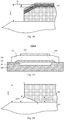
- Fig. 1A is a schematic section view of a bulk acoustic wave resonator according to an exemplary embodiment of the present invention.
- the bulk acoustic wave resonator includes a substrate 100, and an air cavity 101 embedded in the substrate functions as an acoustic mirror.
- the air cavity herein is only a specific embodiment of the acoustic mirror structure, and it is also applicable that the air cavity is replaced with other acoustic mirror structures including a Bragg reflecting layer.
- the bulk acoustic wave resonator 100A further includes a bottom electrode 102, a piezoelectric layer 103 and a top electrode 104.
- the two ends of the bottom electrode 102 extend beyond the range of the air cavity 101 in two opposite directions, so that the two ends of the trapezoidal lower bottom edge of 102 both have parts that are partially in contact with the upper surface of the substrate 100.
- the piezoelectric layer 103 has a stepped structure, which is composed of a first step, a second step and an interface between the two steps, wherein the plane of the first step is higher than the plane of the second step.
- the first step and the interface form a first edge of the piezoelectric layer; and the second step and the interface form a second edge of the piezoelectric layer.
- the piezoelectric layer may not have the stepped structure.
- the main part of the top electrode 104 completely falls within the range of the first step of the piezoelectric layer in the section view, and the top electrode has an axisymmetric detail structure at its two ends 105 at the same time.
- Fig. 1B is an enlarged view of the detail part 105 in Fig. 1A .
- the top electrode 104 is made of Mo in the present embodiment and has a thickness H101, and the range of H101 is 0.1 ⁇ m to 0.6 ⁇ m.
- the height of an inclined edge AB in the vertical direction is H102, and the range of H102 is 0 ⁇ m to 0.6 ⁇ m.
- the inclined edge AB forms an angle ⁇ 101 with the horizontal direction, and the range of ⁇ 101 is 15° to 75°.
- B and C can also overlap.
- a passivation layer 115 is added in Fig. 1C on the basis of Fig. 1B , wherein the material of the passivation layer in the present embodiment can be SiO 2 , the thickness of the passivation layer 115 is H112, and range of H112 is 0.02 ⁇ m to 0.3 ⁇ m.
- a passivation layer is added in Fig. 1D on the basis of Fig. 1B , and at the same time, another layer of metal electrode material 126 is added between the passivation layer and the top electrode.
- this layer of metal material can be chromium (Cr), the thickness of the metal layer 126 is H122, and the range of H122 is 0.04 ⁇ m to 0.24 ⁇ m.
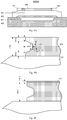
- Fig. 2A is a schematic section view of a bulk acoustic wave resonator according to an exemplary embodiment of the present invention.
- the bulk acoustic wave resonator includes a substrate 200, and an air cavity 201 embedded in the substrate functions as an acoustic mirror.
- the air cavity herein is only a specific embodiment of the acoustic mirror structure, and it is also applicable that the air cavity is replaced with other acoustic mirror structures including a Bragg reflecting layer.
- the bulk acoustic wave resonator 200A further includes a bottom electrode 202, a piezoelectric layer 203 and a top electrode 204.
- the two ends of the bottom electrode 202 extend beyond the range of the air cavity 201 in two opposite directions, so that the two ends of the trapezoidal lower bottom edge of 202 are partially in contact with the upper surface of the substrate 200.
- the piezoelectric layer 203 has a stepped structure, which is composed of a first step, a second step and an interface between the two steps, wherein the plane of the first step is higher than the plane of the second step.
- the first step and the interface form the first edge of the piezoelectric layer; and the second step and the interface form the second edge of the piezoelectric layer.
- the main part of the top electrode 204 completely falls within the range of the first step of the piezoelectric layer in the section view, and the top electrode has an axisymmetric detail structure at its two ends 205 at the same time.
- Fig. 2B is an enlarged view of a detail part 205 in Fig. 2A , wherein the top electrode 204 is made of Mo in the present embodiment and has a thickness H201, and the range of H201 is 0.1 ⁇ m to 0.6 ⁇ m.
- the height of an inclined edge BC in the vertical direction is H202, and the range of H202 is 0 ⁇ m to 0.6 ⁇ m.
- the inclined edge BC forms an angle ⁇ 201 with the horizontal direction, and the range of ⁇ 201 is 15° to 75°.
- a passivation layer 215 is added in Fig. 2C on the basis of Fig. 2B , wherein the material of the passivation layer in the present embodiment can be SiO 2 , the thickness of the passivation layer 215 is H212, and range of H212 is 0.01 ⁇ m to 0.1 ⁇ m.
- a passivation layer is added in Fig. 2D on the basis of Fig. 2B , and at the same time, another layer of metal electrode material 226 is added between the passivation layer and the top electrode.
- this layer of metal material can be chromium (Cr), the thickness of the metal layer 226 is H222, and the range of H222 is 0.04 ⁇ m to 0.24 ⁇ m.
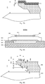
- Fig. 3A is a schematic section view of a bulk acoustic wave resonator according to an exemplary embodiment of the present invention.
- the bulk acoustic wave resonator includes a substrate 300, and an air cavity 301 embedded in the substrate functions as an acoustic mirror.
- the air cavity herein is only a specific embodiment of the acoustic mirror structure, and it is also applicable that the air cavity is replaced with other acoustic mirror structures including a Bragg reflecting layer.
- the bulk acoustic wave resonator 300A further includes a bottom electrode 302, a piezoelectric layer 303 and a top electrode 304.
- the two ends of the bottom electrode 302 extend beyond the range of the air cavity 301 in two opposite directions, so that the two ends of the trapezoidal lower bottom edge of 302 are partially in contact with the upper surface of the substrate 300.
- the piezoelectric layer 303 has a stepped structure, which is composed of a first step, a second step and an interface between the two steps, wherein the plane of the first step is higher than the plane of the second step.
- the first step and the interface form the first edge of the piezoelectric layer; and the second step and the interface form the second edge of the piezoelectric layer.
- the main part of the top electrode 304 completely falls within the range of the first step of the piezoelectric layer in the section view, and the top electrode has an axisymmetric detail structure at its two ends 305 at the same time.
- Fig. 3B is an enlarged view of a detail part 305 in Fig. 3A .
- the top electrode 304 is made of Mo in the present embodiment and has a thickness H301, and the range of H301 is 0. 1 ⁇ m to 0.6 ⁇ m.
- the height of an inclined edge AB in the vertical direction is H302, and the range of H302 is 0 ⁇ m to 0.6 ⁇ m.
- the inclined edge AB forms an angle ⁇ 301 with the horizontal direction, and the range of ⁇ 301 is 15° to 75°.
- the height of an inclined edge CD in the vertical direction is H303, and the range of H303 is 0 ⁇ m to 0.6 ⁇ m.
- the inclined edge CD forms an angle ⁇ 302 with the horizontal direction, and the range of ⁇ 302 is 15° to 75°.
- a passivation layer 315 is added in Fig. 3C on the basis of Fig. 3B , wherein the material of the passivation layer in the present embodiment can be SiO 2 , the thickness of the passivation layer 315 is H312, and range of H312 is 0.01 ⁇ m to 0.1 ⁇ m.
- a passivation layer is added in Fig. 3D on the basis of Fig. 3B , and at the same time, another layer of metal electrode material 326 is added between the passivation layer and the top electrode.
- this layer of metal material can be chromium (Cr), the thickness of the metal layer 326 is H322, and the range of H322 is 0.04 ⁇ m to 0.24 ⁇ m.
- Fig. 4A is a schematic section view of a bulk acoustic wave resonator according to an exemplary embodiment of the present invention.
- the bulk acoustic wave resonator includes a substrate 400, and an air cavity 401 embedded in the substrate functions as an acoustic mirror.
- the air cavity herein is only a specific embodiment of the acoustic mirror structure, and it is also applicable that the air cavity is replaced with other acoustic mirror structures including a Bragg reflecting layer.
- the bulk acoustic wave resonator 400A further includes a bottom electrode 402, a piezoelectric layer 403 and a top electrode 404.
- the two ends of the bottom electrode 402 extend beyond the range of the air cavity 401 in two opposite directions, so that the two ends of the trapezoidal lower bottom edge of 402 are partially in contact with the upper surface of the substrate 400.
- the piezoelectric layer 403 has a stepped structure, which is composed of a first step, a second step and an interface between the two steps, wherein the plane of the first step is higher than the plane of the second step.
- the first step and the interface form the first edge of the piezoelectric layer; and the second step and the interface form the second edge of the piezoelectric layer.
- the main part of the top electrode 404 completely falls within the range of the first step of the piezoelectric layer in the section view, and the top electrode has an axisymmetric detail structure at its two ends 405 at the same time.
- Fig. 4B is an enlarged view of a detail part 405 in Fig. 4A .
- the top electrode 404 is made of Mo in the present embodiment and has a thickness H401, and the range of H401 is 0. 1 ⁇ m to 0.6 ⁇ m.
- the height of a vertical edge AB is H402, and the range of H402 is 0 ⁇ m to 0.6 ⁇ m.
- An inclined edge BC forms an angle ⁇ 401 with the horizontal direction, and the range of ⁇ 401 is 15° to 75°.
- the horizontal distance between a vertical edge AF and a vertical edge CD is D401, and the range of D401 is 0 ⁇ m to 1 ⁇ m.
- An inclined edge DE forms an angle ⁇ 402 with the horizontal direction, and the range of ⁇ 402 is 15° to 75°.
- the height of a vertical edge EF is H403, and the range of H403 is 0 ⁇ m to 0.6 ⁇ m.
- a passivation layer 415 is added in Fig. 4C on the basis of Fig. 4B , wherein the material of the passivation layer in the present embodiment can be SiO 2 , the thickness of the passivation layer 415 is H412, and range of H412 is 0.01 ⁇ m to 0.1 ⁇ m.
- a passivation layer is added in Fig. 4D on the basis of Fig. 4B , and at the same time, another layer of metal electrode material 426 is added between the passivation layer and the top electrode.
- this layer of metal material can be chromium (Cr), the thickness of the metal layer 426 is H422, and the range of H422 is 0.04 ⁇ m to 0.24 ⁇ m.
- Fig. 5A is a schematic section view of a bulk acoustic wave resonator according to an exemplary embodiment of the present invention.
- the bulk acoustic wave resonator includes a substrate 500, and an air cavity 501 embedded in the substrate functions as an acoustic mirror.
- the air cavity herein is only a specific embodiment of the acoustic mirror structure, and it is also applicable that the air cavity is replaced with other acoustic mirror structures including a Bragg reflecting layer.
- the bulk acoustic wave resonator 500A further includes a bottom electrode 502, a piezoelectric layer 503 and a top electrode 504.
- the two ends of the bottom electrode 502 extend beyond the range of the air cavity 501 in two opposite directions, so that the two ends of the trapezoidal lower bottom edge of the bottom electrode 502 are partially in contact with the upper surface of the substrate 500.
- the piezoelectric layer 503 has a stepped structure, which is composed of a first step, a second step and an interface between the two steps, wherein the plane of the first step is higher than the plane of the second step.
- the first step and the interface form the first edge of the piezoelectric layer; and the second step and the interface form the second edge of the piezoelectric layer.
- the main part of the top electrode 504 completely falls within the range of the first step of the piezoelectric layer in the section view, and the top electrode has an axisymmetric detail structure at its two ends 505 at the same time.
- Fig. 5B is an enlarged view of a detail part 505 in Fig. 5A .
- the top electrode 504 is made of Mo in the present embodiment and has a thickness H501, and the range of H501 is 0. 1 ⁇ m to 0.6 ⁇ m.
- the height of an inclined edge AB is H502, the range of H502 is 0 ⁇ m to 0.6 ⁇ m, the inclined edge AB forms an angle ⁇ 501 with the horizontal direction, and the range of ⁇ 501 is 15° to 75°.
- the height of an inclined edge CD is H503, and the range of H503 is 0 ⁇ m to 0.6 ⁇ m.
- the inclined edge CD forms an angle ⁇ 502 with the horizontal direction, and the range of ⁇ 502 is 15° to 75°.
- a passivation layer 515 is added in Fig. 5C on the basis of Fig. 5B , wherein the material of the passivation layer in the present embodiment can be SiO 2 , the thickness of the passivation layer 515 is H512, and range of H512 is 0.01 ⁇ m to 0.1 ⁇ m.
- a passivation layer is added in Fig. 5D on the basis of Fig. 5B , and at the same time, another layer of metal electrode material 526 is added between the passivation layer and the top electrode.
- this layer of metal material can be chromium (Cr), the thickness of the metal layer 526 is H522, and the range of H522 is 0.04 ⁇ m to 0.24 ⁇ m.
- Fig. 6A is a schematic section view of a bulk acoustic wave resonator according to an exemplary embodiment of the present invention.
- the bulk acoustic wave resonator includes a substrate 600, and an air cavity 601 embedded in the substrate functions as an acoustic mirror.
- the air cavity herein is only a specific embodiment of the acoustic mirror structure, and it is also applicable that the air cavity is replaced with other acoustic mirror structures including a Bragg reflecting layer.
- the bulk acoustic wave resonator 600A further includes a bottom electrode 602, a piezoelectric layer 603 and a top electrode 604.
- the two ends of the bottom electrode 602 extend beyond the range of the air cavity 601 in two opposite directions, so that the two ends of the trapezoidal lower bottom edge of the bottom electrode 602 are partially in contact with the upper surface of the substrate 600.
- the piezoelectric layer 603 has a stepped structure, which is composed of a first step, a second step and an interface between the two steps, wherein the plane of the first step is higher than the plane of the second step.
- the first step and the interface form the first edge of the piezoelectric layer; and the second step and the interface form the second edge of the piezoelectric layer.
- the main part of the top electrode 604 completely falls within the range of the first step of the piezoelectric layer in the section view, and the top electrode has an axisymmetric detail structure at its two ends 605 at the same time.
- Fig. 6B is an enlarged view of a detail part 605 in Fig. 6A .
- the top electrode 604 is made of Mo in the present embodiment and has a thickness H601, and the range of H601 is 0. 1 ⁇ m to 0.6 ⁇ m.
- the height of an inclined edge BC is H602, the range of H602 is 0 ⁇ m to 0.6 ⁇ m, the inclined edge BC forms an angle ⁇ 601 with the horizontal direction, and the range of ⁇ 601 is 15° to 75°.
- the transverse length of a horizontal edge CD is D601, and the range of D601 is 0 ⁇ m to 2 ⁇ m.
- the height of an inclined edge DE is H603, and the range of H603 is 0 ⁇ m to 0.6 ⁇ m.
- the inclined edge DE forms an angle ⁇ 602 with the horizontal direction, and the range of ⁇ 602 is 15° to 75°.
- a passivation layer 615 is added in Fig. 6C on the basis of Fig. 6B , wherein the material of the passivation layer in the present embodiment can be SiO 2 , the thickness of the passivation layer 615 is H612, and range of H612 is 0.01 ⁇ m to 0.1 ⁇ m.
- a passivation layer is added in Fig. 6D on the basis of Fig. 6B , and at the same time, another layer of metal electrode material 626 is added between the passivation layer and the top electrode.
- this layer of metal material can be chromium (Cr), the thickness of the metal layer 626 is H622, and the range of H622 is 0.04 ⁇ m to 0.24 ⁇ m.
- Fig. 7A is a schematic section view of a bulk acoustic wave resonator according to an exemplary embodiment of the present invention.
- the bulk acoustic wave resonator includes a substrate 700, and an air cavity 701 embedded in the substrate functions as an acoustic mirror.
- the air cavity herein is only a specific embodiment of the acoustic mirror structure, and it is also applicable that the air cavity is replaced with other acoustic mirror structures including a Bragg reflecting layer.
- the bulk acoustic wave resonator 700A further includes a bottom electrode 702, a piezoelectric layer 703 and a top electrode 704.
- the two ends of the bottom electrode 702 extend beyond the range of the air cavity 701 in two opposite directions, so that the two ends of the trapezoidal lower bottom edge of 702 are partially in contact with the upper surface of the substrate 700.
- the piezoelectric layer 703 has a stepped structure, which is composed of a first step, a second step and an interface between the two steps, wherein the plane of the first step is higher than the plane of the second step.
- the first step and the interface form the first edge of the piezoelectric layer; and the second step and the interface form the second edge of the piezoelectric layer.
- the main part of the top electrode 704 completely falls within the range of the first step of the piezoelectric layer in the section view, and the top electrode has an axisymmetric detail structure at its two ends 705 at the same time.
- Fig. 7B is an enlarged view of a detail part 705 in Fig. 7A .
- the top electrode 704 is made of Mo in the present embodiment and has a thickness H701, and the range of H701 is 0. 1 ⁇ m to 0.6 ⁇ m.
- the height of a vertical edge CD is H702, and the range of H702 is 0 ⁇ m to 0.6 ⁇ m.
- the height of an inclined edge DE is H703, the range of H703 is 0 ⁇ m to 0.6 ⁇ m, the inclined edge DE forms an angle ⁇ 702 with the horizontal direction, and the range of ⁇ 702 is 15° to 75°.
- the transverse length of a horizontal edge EF is D702, and the range of D702 is 0 ⁇ m to 2 ⁇ m.
- An inclined edge FG forms an angle ⁇ 703 with the horizontal direction, and the range of ⁇ 703 is 15° to 75°.
- the length of a horizontal edge BC in the horizontal direction is D701, and the range of D701 is 0 ⁇ m to 3 ⁇ m.
- the height of an inclined edge AB is H704, and the range of H704 is 0 ⁇ m to 0.5 ⁇ m.
- the inclined edge AB forms an angle ⁇ 701 with the horizontal direction, and the range of ⁇ 701 is 15° to 75°.
- a passivation layer 715 is added in Fig. 7C on the basis of Fig. 7B , wherein the material of the passivation layer in the present embodiment can be SiO 2 , the thickness of the passivation layer 715 is H712, and range of H712 is 0.01 ⁇ m to 0.1 ⁇ m.
- a passivation layer is added in Fig. 7D on the basis of Fig. 7B , and at the same time, another layer of metal electrode material 726 is added between the passivation layer and the top electrode.
- this layer of metal material can be chromium (Cr), the thickness of the metal layer 726 is H722, and the range of H722 is 0.04 ⁇ m to 0.24 ⁇ m.
- Fig. 8A is a schematic section view of a bulk acoustic wave resonator according to an exemplary embodiment of the present invention.
- the bulk acoustic wave resonator includes a substrate 800, and an air cavity 801 embedded in the substrate functions as an acoustic mirror.
- the air cavity herein is only a specific embodiment of the acoustic mirror structure, and it is also applicable that the air cavity is replaced with other acoustic mirror structures including a Bragg reflecting layer.
- the bulk acoustic wave resonator 800A further includes a bottom electrode 802, a piezoelectric layer 803 and a top electrode 804.
- the two ends of the bottom electrode 802 extend beyond the range of the air cavity 801 in two opposite directions, so that the two ends of the trapezoidal lower bottom edge of 802 are partially in contact with the upper surface of the substrate 800.
- the piezoelectric layer 803 has a stepped structure, which is composed of a first step, a second step and an interface between the two steps, wherein the plane of the first step is higher than the plane of the second step.
- the first step and the interface form the first edge of the piezoelectric layer; and the second step and the interface form the second edge of the piezoelectric layer.
- the main part of the top electrode 804 completely falls within the range of the first step of the piezoelectric layer in the section view, and the top electrode has an axisymmetric detail structure at its two ends 805 at the same time.
- Fig. 8B is an enlarged view of a detail part 705 in Fig. 8A .
- the top electrode 804 is made of Mo in the present embodiment and has a thickness H801, and the range of H801 is 0. 1 ⁇ m to 0.6 ⁇ m.
- the height of an inclined edge CD is H805, and the range of H805 is 0 ⁇ m to 0.6 ⁇ m.
- the inclined edge CD forms an angle ⁇ 804 with the horizontal direction, and the range of ⁇ 804 is 15° to 75°.
- the height of a vertical edge DE is H802, and the range of H802 is 0 ⁇ m to 0.6 ⁇ m.
- the height of an inclined edge EF is H803, and the range of H803 is 0 ⁇ m to 0.6 ⁇ m.
- the inclined edge EF forms an angle ⁇ 802 with the horizontal direction, and the range of ⁇ 802 is 15° to 75°.
- the length of a horizontal edge FG in the horizontal direction is D802, and the range of D802 is 0 ⁇ m to 1 ⁇ m.
- An inclined edge GH forms an angle ⁇ 803 with the horizontal direction, and the range of ⁇ 803 is 15° to 75°.
- the horizontal distance from a point B to the vertical edge DE is D801, and the range of D801 is 0 ⁇ m to 2 ⁇ m.
- the height of an inclined edge AB is H804, and the range of H804 is 0 ⁇ m to 0 5 ⁇ m.
- the inclined edge AB forms an angle ⁇ 801 with the horizontal direction, and the range of ⁇ 801 is 15° to 75°.
- a passivation layer 815 is added in Fig. 8C on the basis of Fig. 8B , wherein the material of the passivation layer in the present embodiment can be SiO 2 , the thickness of the passivation layer 815 is H812, and range of H812 is 0.01 ⁇ m to 0.1 ⁇ m.
- a passivation layer is added in Fig. 8D on the basis of Fig. 8B , and at the same time, another layer of metal electrode material 826 is added between the passivation layer and the top electrode.
- this layer of metal material can be chromium (Cr), the thickness of the metal layer 826 is H822, and the range of H822 is 0.04 ⁇ m to 0.24 ⁇ m.
- Fig. 9A is a schematic section view of a bulk acoustic wave resonator according to an exemplary embodiment of the present invention.
- the bulk acoustic wave resonator includes a substrate 900, and an air cavity 901 embedded in the substrate functions as an acoustic mirror.
- the air cavity herein is only a specific embodiment of the acoustic mirror structure, and it is also applicable that the air cavity is replaced with other acoustic mirror structures including a Bragg reflecting layer.
- the bulk acoustic wave resonator 900A further includes a bottom electrode 902, a piezoelectric layer 903 and a top electrode 904.
- the two ends of the bottom electrode 902 extend beyond the range of the air cavity 901 in two opposite directions, so that the two ends of the trapezoidal lower bottom edge of 902 are partially in contact with the upper surface of the substrate 900.
- the piezoelectric layer 903 has a stepped structure, which is composed of a first step, a second step and an interface between the two steps, wherein the plane of the first step is higher than the plane of the second step.
- the first step and the interface form the first edge of the piezoelectric layer; and the second step and the interface form the second edge of the piezoelectric layer.
- the main part of the top electrode 904 completely falls within the range of the first step of the piezoelectric layer in the section view, and the top electrode has an axisymmetric detail structure at its two ends 905 at the same time.
- Fig. 9B is an enlarged view of a detail part 905 in Fig. 9A .
- the top electrode 904 is made of Mo in the present embodiment and has a thickness H901, and the range of H901 is 0. 1 ⁇ m to 0.6 ⁇ m.
- the height of an inclined edge AB is H902, and the range of H902 is 0 ⁇ m to 0.4 ⁇ m.
- the inclined edge AB forms an angle ⁇ 901 with the horizontal direction, and the range of ⁇ 901 is 15° to 75°.
- the length of a horizontal edge CD is D901, and the range of D901 is 0 ⁇ m to 2 ⁇ m.
- the height of an inclined edge DE is H903, and the range of H903 is 0.2 ⁇ m to 0.6 ⁇ m.
- DE forms an included angle ⁇ 902 with the horizontal direction, and the range of ⁇ 902 is 15° to 75°.
- the height of a horizontal edge AF is D902, and the range of D902 is 0 ⁇ m to 2 ⁇ m.
- An inclined edge FG is parallel to DE.
- the vertical height from a point G to a point E is H904, and the range of H904 is 0. 1 ⁇ m to 0.6 ⁇ m.
- the structure of the end face ABC adopts the structure of the solutions in Fig.1A to Fig.1B , and this is only an example and is not used to limit the use possibilities of the other solutions involved in the specification.
- a passivation layer 915 is added in Fig. 9C on the basis of Fig. 9B , wherein the material of the passivation layer in the present embodiment can be SiO 2 , the thickness of the passivation layer 915 is H912, and range of H912 is 0.01 ⁇ m to 0.1 ⁇ m.
- a passivation layer is added in Fig. 9D on the basis of Fig. 9B , and at the same time, another layer of metal electrode material 926 is added between the passivation layer and the top electrode.
- this layer of metal material can be chromium (Cr), the thickness of the metal layer 926 is H922, and the range of H922 is 0.04 ⁇ m to 0.24 ⁇ m.
- Fig. 10A is a schematic section view of a bulk acoustic wave resonator according to an exemplary embodiment of the present invention.
- the bulk acoustic wave resonator includes a substrate 1000, and an air cavity 1001 embedded in the substrate functions as an acoustic mirror.
- the air cavity herein is only a specific embodiment of the acoustic mirror structure, and it is also applicable that the air cavity is replaced with other acoustic mirror structures including a Bragg reflecting layer.
- the bulk acoustic wave resonator 1000A further includes a bottom electrode 1002, a piezoelectric layer 1003 and a top electrode 1004.
- the two ends of the bottom electrode 1002 extend beyond the range of the air cavity 1001 in two opposite directions, so that the two ends of the trapezoidal lower bottom edge of 1002 are partially in contact with the upper surface of the substrate 1000.
- the piezoelectric layer 1003 has a stepped structure, which is composed of a first step, a second step and an interface between the two steps, wherein the plane of the first step is higher than the plane of the second step.
- the first step and the interface form the first edge of the piezoelectric layer; and the second step and the interface form the second edge of the piezoelectric layer.
- the main part of the top electrode 1004 completely falls within the range of the first step of the piezoelectric layer in the section view, and the top electrode has an axisymmetric detail structure at its two ends 1005 at the same time.
- Fig. 10B is an enlarged view of a detail part 1005 in Fig. 10A .
- the top electrode 1004 is made of Mo in the present embodiment and has a thickness H1001, and the range of H1001 is 0.1 ⁇ m to 0.6 ⁇ m.
- a circular arc AB has a radius R1001, and the range of R1001 is 0.3 ⁇ m to 20 ⁇ m.
- the horizontal distance between the circle center O and an upper end pointA is D1001
- the vertical distance is H1002
- the range of D1001 is 0 ⁇ m to 10 ⁇ m
- the range of H1002 is 0 ⁇ m to 0.6 ⁇ m.
- the AB segment can be a circular arc or other smooth protruding shapes.
- a passivation layer 1015 is added in Fig. 10C on the basis of Fig. 10B , wherein the material of the passivation layer in the present embodiment can be SiO 2 , the thickness of the passivation layer 1015 is H1012, and range of H1012 is 0.01 ⁇ m to 0.1 ⁇ m.
- a passivation layer is added in Fig. 10D on the basis of Fig. 10B , and at the same time, another layer of metal electrode material 1026 is added between the passivation layer and the top electrode.
- this layer of metal material can be chromium (Cr), the thickness of the metal layer 1026 is H1022, and the range of H1022 is 0.04 ⁇ m to 0.24 ⁇ m.
- the structure shown in Fig. 9B is a typical suspension wing structure.
- the detail structure in the above-mentioned embodiment can also be arranged on the suspension wing structure.
- At least a part of at least one of the upper and lower surfaces of at least one end of the top electrode is an inclined surface.
- At least one of the upper and lower surfaces of at least one end of the top electrode includes: an inclined surface, and a vertical extension surface and/or a horizontal extension surface.
- the vertical extension surface here can be, for example, the AB surface in Fig. 6B
- the horizontal extension surface can be, for example, the CD surface in Fig. 6B .
- the length range in the horizontal direction is 0.02 ⁇ m to 3 ⁇ m, for example, 0.02 ⁇ m, 2 ⁇ m, or 3 ⁇ m.
- the length can be used for determining the bandwidth range of a repressible parasitic mode.
- Fig. 11A is a schematic section view of a bulk acoustic wave resonator according to an exemplary embodiment of the present invention.
- the bulk acoustic wave resonator includes a substrate 1100, and an air cavity 1101 embedded in the substrate functions as an acoustic mirror.
- the air cavity herein is only a specific embodiment of the acoustic mirror structure, and it is also applicable that the air cavity is replaced with other acoustic mirror structures including a Bragg reflecting layer.
- the bulk acoustic wave resonator 1100A further includes a bottom electrode 1102, a piezoelectric layer 1103 and a top electrode 1104.
- the two ends of the bottom electrode 1102 extend beyond the range of the air cavity 1101 in two opposite directions, so that the two ends of the trapezoidal lower bottom edge of 1102 are partially in contact with the upper surface of the substrate 1100.
- the piezoelectric layer 1103 has a stepped structure, which is composed of a first step, a second step and an interface between the two steps, wherein the plane of the first step is higher than the plane of the second step.
- the first step and the interface form the first edge of the piezoelectric layer; and the second step and the interface form the second edge of the piezoelectric layer.
- the main part of the top electrode 1104 completely falls within the range of the first step of the piezoelectric layer in the section view, and the top electrode has an axisymmetric detail structure at its two ends 1105 at the same time.
- the upper part of the top electrode 1104 is covered with a passivation layer 1106.
- the material of 1106 is aluminum nitride (A1N).
- the end face of 1106 is located on the outer side of the end face of 1104.
- Fig. 11B is an enlarged view of a detail part 1105 in Fig. 11A .
- the top electrode 1104 adopts a traditional structure
- the passivation layer 1106 adopts the structure of solution (1).
- the solution combination in the present embodiment is only an exemplary embodiment, and is not used to limit the use possibilities of the other solution combinations involved in the specification.
- the thickness of the electrode 1104 is H1101, and the range of H1101 is 0.1 ⁇ m to 0.6 ⁇ m.
- the thickness H1102 of the passivation layer 1106 is 0.04 ⁇ m to 0.24 ⁇ m.
- the range of the height H1103 of an inclined edge AB is 0 ⁇ m to 0.24 ⁇ m.
- the range of the included angle ⁇ 1101 formed by the edge AB and the horizontal direction is 15° to 75°.
- the distance of the passivation layer 1106 extending to the outer side of the electrode 1104 in the horizontal direction is D1101, and the range of D1101 is 0.1 ⁇ m to 3 ⁇ m.
- the mentioned numerical range can also be a median value between the endpoint values or other values, and all of which fall within the protection scope of the present invention.
- the embodiment of the present invention proposes a bulk acoustic wave resonator, including: a substrate; an acoustic mirror; a bottom electrode arranged above the substrate; a top electrode opposed to the bottom electrode; and a piezoelectric layer arranged above the bottom electrode and between the bottom electrode and the top electrode, wherein at least one of the two ends of the top electrode is provided with a transverse mode vibration suppression structure.
- the present invention proposes that at least one of the two ends of the top electrode is provided with the transverse mode vibration suppression structure.
- the transverse mode vibration suppression structure can be a non-parallel structure of upper and lower surfaces arranged at the end part of the top electrode. Further, the non-parallel structure of upper and lower surfaces can be an inclined surface chamfer structure.
- the inclined surface chamfer structure introduces an obtuse angle structure into the cross section geometry structure, thereby being conducive to preventing the parasitic mode from forming standing waves.
- the inclined surface chamfer structure is a continuously changing structure in space, which can suppress the parasitic mode within a wider bandwidth range compared with the traditional parallel structure, and at the same time, the bandwidth range can be adjusted according to the shape and size of the continuously changing structure.
- the transverse mode vibration suppression structure can also be a non-vertical surface that is arranged at the end face of at least one end of the top electrode and is different from a vertical surface, such as a concave surface or a convex surface, and this is also conducive to preventing the parasitic mode from forming standing waves.
- the material of the substrate includes, but not limited to: monocrystalline silicon (Si), gallium arsenide (GaAs), sapphire, quartz, or the like.
- the electrode materials used in the present invention can include, but not limited to: molybdenum (Mo), chromium (Cr), gold (Au), tungsten (W), aluminum (Al), platinum (Pt), ruthenium (Ru), etc.
- the passivation layer is made of dielectric material, and the dielectric material can be selected from, but not limited to: silicon dioxide (SiO 2 ), silicon nitride (Si 3 N 4 ), silicon carbide (SiC), aluminum nitride (AlN), aluminum oxide (Al 2 O 3 ) and so on.
- the material adopted by the acoustic mirror in the form of the Bragg reflecting layer in the present invention includes, but not limited to: molybdenum (Mo), aluminum nitride (A1N), tungsten (W), silicon dioxide, and the like.
- the hollow cavity type acoustic mirror adopted in the present invention can also be filled with a dielectric material, wherein the specific material can include, but not limited to: silicon oxide (silicon oxide), silicon nitride (silicon nitride), silicon carbide (silicon carbide) and other suitable dielectric materials.
- the dielectric layer is made of a "dielectric material with a low dielectric constant" such as porous silica (porous silica), fluorinated amorphous carbon (fluorinated amorphous carbon), fluoro-polymer (fluoro-polymer), parylene (parylene), polyarylene ether (polyarylene ether), hydrogen silsesquioxane (HSQ), cross-linked polyphenylene polymer (SiLK), diphenylcyclobutene (BCB), fluorinated silicon dioxide (fluorinated silicon dioxide), carbon dopedoxide (carbon dopedoxide) or diamond like carbon (diamond like carbon).
- the "dielectric material with the low dielectric constant” refers to a dielectric material with a dielectric constant less than that of silicon dioxide.
- the material of the piezoelectric film adopted in the present invention includes, but not limited to: aluminum nitride (A1N), zinc oxide (ZnO), and doped aluminum nitride (A1RN) with a certain atomic ratio, wherein the doping element R includes, but not limited to: scandium (Sc), magnesium (Mg), titanium (Ti), etc.
- a passivation layer of a certain thickness can be added to a part of upper surface of the top electrode, and the optional material of the cover layer can include dielectric materials such as silicon dioxide and silicon nitride.
- the embodiment of the present invention further relates to a filter, including the above-mentioned bulk acoustic wave resonator.
- the embodiment of the present invention further relates to an electronic device, including the above-mentioned filter.
- the electronic device here includes, but not limited to, intermediate products such as radio frequency front-ends, filter amplifier modules, and terminal products such as mobile phones, WIFI, and unmanned aerial vehicles.
Landscapes
- Physics & Mathematics (AREA)
- Acoustics & Sound (AREA)
- Engineering & Computer Science (AREA)
- Manufacturing & Machinery (AREA)
- Piezo-Electric Or Mechanical Vibrators, Or Delay Or Filter Circuits (AREA)
Abstract
Description
- Embodiments of the present invention relate to the field of semiconductors, in particular to a bulk acoustic wave resonator, a filter having the resonator, and an electronic device having the filter.
- A film bulk wave resonator made by the longitudinal resonance of a piezoelectric film in the thickness direction has become a feasible alternative to surface acoustic wave devices and quartz crystal resonators in terms of machine communication and high-speed serial data applications. A radio frequency front end bulk wave filter/duplexer provides superior filtering characteristics, such as low insertion loss, steep transition band, higher power capacity, and stronger electrostatic discharge (ESD) resistance. A high-frequency film bulk wave oscillator with ultra-low frequency temperature drift has low phase noise, low power consumption and a large bandwidth modulation range. In addition, these miniature film resonators use CMOS-compatible processing technology on silicon substrates, which can reduce the unit cost and facilitate the final integration with CMOS circuits.
- The bulk wave resonator includes an acoustic mirror, two electrodes, and a piezoelectric material layer called piezoelectric excitation between the two electrodes. A bottom electrode and a top electrode are also called excitation electrodes, and their function is to cause mechanical oscillation of each layer of the resonator. An acoustic mirror forms acoustic isolation between the bulk wave resonator and the substrate to prevent acoustic waves from being conducted to the outside of the resonator to cause energy loss.
- The example 1200A in
Fig. 12A is a top view of a traditional bulk acoustic wave resonator. Theacoustic mirror 1201 is composed of an air cavity on the substrate, and its function is to approximately convert the acoustic impedance of the substrate into the acoustic impedance of air. Most of the bottom electrode (not shown here) should be located on the inner side of the boundary of theacoustic mirror 1201. The bottom electrode is covered with apiezoelectric film 1203, and the boundary of the piezoelectric film is located on the outer side of the boundary of the acoustic mirror. The piezoelectric layer is covered with atop electrode 1204, and the top electrode has an extendedend 1205 at the same time. - The example 1201A in
Fig. 12B is a schematic section view of the example 1200A at AA'. The structure includes asubstrate 1210, anacoustic mirror 1211, abottom electrode 1212, apiezoelectric layer 1213 and atop electrode 1214. - In an ideal state, the energy of an alternating electrical signal applied to the top electrode and the bottom electrode is only converted into the acoustic energy of a longitudinal vibration mode (usually called a piston mode) of the piezoelectric layer. In actual situations, along with the longitudinal vibration mode, acoustic waves in a transverse vibration mode are also generated, the existence of the waves in the transverse vibration mode will weaken the energy of the acoustic waves in the piston mode, thereby resulting in serious deterioration in the key performance parameters of the device such as quality factor (Q) and effective electromechanical coupling factor (K2 t,eff ). At the same time, the filter constructed by the bulk acoustic wave resonator also generates noise on a filter frequency characteristic curve, thereby reducing the performance of the filter system.
- Generally, the transverse mode is parasitic in the entire space formed by the upper bottom electrode and the piezoelectric layer. Especially when the geometrical shape of the cross section of the film layer has parallel sides in pairs, the transverse mode will be enhanced because of the formation of standing waves.
- In the example 1201A of the traditional bulk acoustic wave resonator, the top electrode has a rectangular cross section structure, the structure is suitable for acoustic waves in the parasitic mode to form stable standing waves therein, so that the acoustic waves in the parasitic mode occupy considerable energy, which seriously affects the performance of the resonator. Therefore, the structure of the top electrode structure needs to be improved to improve the performance of the resonator.
- In order to suppress or further reduce the parasitism of acoustic waves in a transverse mode in the top electrode structure in a bulk acoustic wave resonator, the present invention is proposed.
- According to one aspect of an embodiment of the present invention, a bulk acoustic wave resonator is proposed, including: a substrate; an acoustic mirror; a bottom electrode arranged above the substrate; a top electrode opposed to the bottom electrode; and a piezoelectric layer arranged above the bottom electrode and between the bottom electrode and the top electrode, wherein at least one of the two ends of the top electrode is provided with a transverse mode vibration suppression structure.
- Optionally, the suppression structure includes a non-parallel structure of upper and lower surfaces arranged on at least one of the two ends of the top electrode.
- Optionally, at least a part of at least one of the upper and lower surfaces of at least one end of the top electrode is an inclined surface.
- Further, the angle formed by the inclined surface and the surface of the substrate is 15-75 degrees.
- Further, the length of the inclined surface in the horizontal direction ranges from 0.02µm to 3µm.
- Or further, at least one of the upper and lower surfaces of at least one end of the top electrode includes: a vertical extension surface and/or a horizontal extension surface; and the inclined surface.
- Optionally, the suppression structure includes a non-vertical surface that is arranged at the end face of at least one end of the top electrode and is different from a vertical surface, wherein the vertical surface is perpendicular to the surface of the substrate. Further optionally, the non-vertical surface has a shape of a concave surface or a convex surface.
- Optionally, the above-mentioned resonator further includes a passivation layer arranged on the top electrode. Further, the thickness of the passivation layer is 0.01µm to 0. 1um.
- Optionally, the above-mentioned resonator further includes a metal electrode material layer and a passivation layer, which are sequentially arranged on the top electrode. Further, the thickness of the metal electrode material layer is 0.04µm to 0.24µm.
- Optionally, at least one end part of the top electrode comprises a suspension wing structure, and the suspension wing structure includes the suppression structure.
- Optionally, the two ends of the top electrode are axisymmetric structures to each other.
- Optionally, the resonator further includes a passivation layer, and the passivation layer is disposed to cover the top electrode, wherein: at least one end of the passivation layer extends beyond the corresponding end of the top electrode; and the end of the passivation layer extending beyond the corresponding end of the top electrode is provided with the suppression structure.
- Optionally, the suppression structure includes a non-parallel structure of upper and lower surfaces of the passivation layer; and/or the suppression structure includes a non-vertical structure that is arranged at the end face of at least one end of the passivation layer and is different from the vertical surface, wherein the vertical surface is perpendicular to the surface of the substrate.
- Optionally, at least one end part of the top electrode comprises a suspension wing structure.
- Optionally, the two ends of the passivation layer extend beyond the corresponding end parts of the top electrode and are axisymmetric structures to each other.
- Optionally, the distance of the end part of the passivation layer extending beyond the top electrode is 0.1µm to 3µm.
- Optionally, the thickness of the passivation layer is 0.04µm to 0.24µm.
- The embodiment of the present invention further relates to a filter, including the above-mentioned bulk acoustic wave resonator.
- The embodiment of the present invention further relates to an electronic device, including the above-mentioned filter.
- The following descriptions and drawings can better help understand these and other features and advantages in various embodiments disclosed in the present invention. The same reference signs in the drawings always indicate the same components, wherein:
-
Fig. 1A is a schematic section view of a bulk acoustic wave resonator according to an exemplary embodiment of the present invention; -
Fig. 1B is an enlarged view of a detail part inFig. 1A ; -
Fig. 1C is an enlarged view of adding a passivation layer on the basis of the structure ofFig. 1B ; -
Fig. 1D is an enlarged view of adding a passivation layer and a metal electrode material layer on the basis of the structure ofFig. 1B ; -
Fig. 2A is a schematic section view of a bulk acoustic wave resonator according to an exemplary embodiment of the present invention; -
Fig. 2B is an enlarged view of a detail part inFig. 2A ; -
Fig. 2C is an enlarged view of adding a passivation layer on the basis of the structure ofFIG. 2B ; -
Fig. 2D is an enlarged view of adding a passivation layer and a metal electrode material layer on the basis of the structure ofFig. 2B ; -
Fig. 3A is a schematic section view of a bulk acoustic wave resonator according to an exemplary embodiment of the present invention; -
Fig. 3B is an enlarged view of a detail part inFig. 3A ; -
Fig. 3C is an enlarged view of adding a passivation layer on the basis of the structure ofFig. 3B ; -
Fig. 3D is an enlarged view of adding a passivation layer and a metal electrode material layer on the basis of the structure ofFig. 3B ; -
Fig. 4A is a schematic section view of a bulk acoustic wave resonator according to an exemplary embodiment of the present invention; -
Fig. 4B is an enlarged view of a detail part inFig. 4A ; -
Fig. 4C is an enlarged view of adding a passivation layer on the basis of the structure ofFig. 4B ; -
Fig. 4D is an enlarged view of adding a passivation layer and a metal electrode material layer on the basis of the structure ofFig. 4B ; -
Fig. 5A is a schematic section view of a bulk acoustic wave resonator according to an exemplary embodiment of the present invention; -
Fig. 5B is an enlarged view of a detail part inFig. 5A ; -
Fig. 5C is an enlarged view of adding a passivation layer on the basis of the structure ofFig. 5B ; -
Fig. 5D is an enlarged view of adding a passivation layer and a metal electrode material layer on the basis of the structure ofFig. 5B ; -
Fig. 6A is a schematic section view of a bulk acoustic wave resonator according to an exemplary embodiment of the present invention; -
Fig. 6B is an enlarged view of a detail part inFig. 6A ; -
Fig. 6C is an enlarged view of adding a passivation layer on the basis of the structure ofFig. 6B ; -
Fig. 6D is an enlarged view of adding a passivation layer and a metal electrode material layer on the basis of the structure ofFig. 6B ; -
Fig. 7A is a schematic section view of a bulk acoustic wave resonator according to an exemplary embodiment of the present invention; -
Fig. 7B is an enlarged view of a detail part inFig. 7A ; -
Fig. 7C is an enlarged view of adding a passivation layer on the basis of the structure ofFig. 7B ; -
Fig. 7D is an enlarged view of adding a passivation layer and a metal electrode material layer on the basis of the structure ofFig. 7B ; -
Fig. 8A is a schematic section view of a bulk acoustic wave resonator according to an exemplary embodiment of the present invention; -
Fig. 8B is an enlarged view of a detail part inFig. 8A ; -
Fig. 8C is an enlarged view of adding a passivation layer on the basis of the structure ofFig. 8B ; -
Fig. 8D is an enlarged view of adding a passivation layer and a metal electrode material layer on the basis of the structure ofFig. 8B ; -
Fig. 9A is a schematic section view of a bulk acoustic wave resonator according to an exemplary embodiment of the present invention; -
Fig. 9B is an enlarged view of a detail part inFig. 9A ; -
Fig. 9C is an enlarged view of adding a passivation layer on the basis of the structure ofFig. 9B ; -
Fig. 9D is an enlarged view of adding a passivation layer and a metal electrode material layer on the basis of the structure ofFig. 9B ; -
Fig. 10A is a schematic section view of a bulk acoustic wave resonator according to an exemplary embodiment of the present invention; -
Fig. 10B is an enlarged view of a detail part inFig. 10A ; -
Fig. 10C is an enlarged view of adding a passivation layer on the basis of the structure ofFig. 10B ; -
Fig. 10D is an enlarged view of adding a passivation layer and a metal electrode material layer on the basis of the structure ofFig. 10B ; -
Fig. 11A is a schematic section view of a bulk acoustic wave resonator according to an exemplary embodiment of the present invention; -
Fig. 11B is an enlarged view of a detail part inFig. 11A ; -
Fig. 12A is a schematic top view of a bulk acoustic wave resonator in the prior art; -
Fig. 12B is a schematic section view cut along the line AA' inFig. 12A . - The technical solutions of the present invention will be further described below in detail through the embodiments and in conjunction with the drawings. In the specification, the same or similar reference signs indicate the same or similar components. The following description of the embodiments of the present invention with reference to the drawings is intended to explain the general inventive concept of the present invention, and should not be construed as a limitation to the present invention.
- Since the transverse vibration mode usually forms stable standing waves between parallel sides in pairs, a detail structure is arranged at the end part of a top electrode of a bulk acoustic wave resonator in the present invention, for example, this kind of detail structure can effectively eliminate or reduce the parallelism of the opposite sides, and destroy the condition or geometric structure of the transverse acoustic vibration mode to form the standing waves in the top electrode, thereby effectively suppressing the parasitic transverse mode vibration in the top electrode, so that more transverse mode vibration energy can be converted into useful piston mode vibration energy, and the Q value of the resonator is improved as a result.
- In the present invention, a dispersion curve near the resonance frequency is optimized by introducing different materials to from a composite top electrode, and at the same time, the resistance of the metal material of the top electrode to the penetration of oxygen and other impurity elements is improved, therefore the Q value and the electromechanical coupling coefficient of the resonator are further improved.
- Hereinafter, a bulk acoustic wave resonator according to an embodiment of the present invention will be described with reference to
Figs. 1A-11B . -
Fig. 1A is a schematic section view of a bulk acoustic wave resonator according to an exemplary embodiment of the present invention. As shown inFig. 1A , the bulk acoustic wave resonator includes asubstrate 100, and anair cavity 101 embedded in the substrate functions as an acoustic mirror. The air cavity herein is only a specific embodiment of the acoustic mirror structure, and it is also applicable that the air cavity is replaced with other acoustic mirror structures including a Bragg reflecting layer. - The bulk
acoustic wave resonator 100A further includes abottom electrode 102, apiezoelectric layer 103 and atop electrode 104. The two ends of thebottom electrode 102 extend beyond the range of theair cavity 101 in two opposite directions, so that the two ends of the trapezoidal lower bottom edge of 102 both have parts that are partially in contact with the upper surface of thesubstrate 100. - The
piezoelectric layer 103 has a stepped structure, which is composed of a first step, a second step and an interface between the two steps, wherein the plane of the first step is higher than the plane of the second step. The first step and the interface form a first edge of the piezoelectric layer; and the second step and the interface form a second edge of the piezoelectric layer. - It should be pointed out that in the present invention, the piezoelectric layer may not have the stepped structure.
- The main part of the
top electrode 104 completely falls within the range of the first step of the piezoelectric layer in the section view, and the top electrode has an axisymmetric detail structure at its twoends 105 at the same time. -
Fig. 1B is an enlarged view of thedetail part 105 inFig. 1A . Thetop electrode 104 is made of Mo in the present embodiment and has a thickness H101, and the range of H101 is 0.1µm to 0.6µm. The height of an inclined edge AB in the vertical direction is H102, and the range of H102 is 0µm to 0.6µm. The inclined edge AB forms an angle α101 with the horizontal direction, and the range of α101 is 15° to 75°. In the embodiment of the present invention, B and C can also overlap. - In order to prevent the top electrode from being corroded by oxygen and water vapor in the air, a
passivation layer 115 is added inFig. 1C on the basis ofFig. 1B , wherein the material of the passivation layer in the present embodiment can be SiO2, the thickness of thepassivation layer 115 is H112, and range of H112 is 0.02µm to 0.3µm. - In order to further improve the dispersion curve of the resonator near the series resonance frequency and/or prevent, for example, the oxygen element in the silicon dioxide passivation layer from diffusing to the top electrode layer, a passivation layer is added in
Fig. 1D on the basis ofFig. 1B , and at the same time, another layer ofmetal electrode material 126 is added between the passivation layer and the top electrode. In the present embodiment, this layer of metal material can be chromium (Cr), the thickness of themetal layer 126 is H122, and the range of H122 is 0.04µm to 0.24µm. -
Fig. 2A is a schematic section view of a bulk acoustic wave resonator according to an exemplary embodiment of the present invention. As shown inFig. 2A , the bulk acoustic wave resonator includes asubstrate 200, and anair cavity 201 embedded in the substrate functions as an acoustic mirror. The air cavity herein is only a specific embodiment of the acoustic mirror structure, and it is also applicable that the air cavity is replaced with other acoustic mirror structures including a Bragg reflecting layer. - The bulk
acoustic wave resonator 200A further includes abottom electrode 202, apiezoelectric layer 203 and atop electrode 204. The two ends of thebottom electrode 202 extend beyond the range of theair cavity 201 in two opposite directions, so that the two ends of the trapezoidal lower bottom edge of 202 are partially in contact with the upper surface of thesubstrate 200. - The
piezoelectric layer 203 has a stepped structure, which is composed of a first step, a second step and an interface between the two steps, wherein the plane of the first step is higher than the plane of the second step. The first step and the interface form the first edge of the piezoelectric layer; and the second step and the interface form the second edge of the piezoelectric layer. - The main part of the
top electrode 204 completely falls within the range of the first step of the piezoelectric layer in the section view, and the top electrode has an axisymmetric detail structure at its twoends 205 at the same time. -
Fig. 2B is an enlarged view of adetail part 205 inFig. 2A , wherein thetop electrode 204 is made of Mo in the present embodiment and has a thickness H201, and the range of H201 is 0.1µm to 0.6µm. The height of an inclined edge BC in the vertical direction is H202, and the range of H202 is 0µm to 0.6µm. The inclined edge BC forms an angle α201 with the horizontal direction, and the range of α201 is 15° to 75°. - In order to prevent the top electrode from being corroded by oxygen and water vapor in the air, a
passivation layer 215 is added inFig. 2C on the basis ofFig. 2B , wherein the material of the passivation layer in the present embodiment can be SiO2, the thickness of thepassivation layer 215 is H212, and range of H212 is 0.01µm to 0.1µm. - In order to further improve the dispersion curve of the resonator near the series resonance frequency and prevent the oxygen element in the silicon dioxide passivation layer from diffusing to the top electrode layer, a passivation layer is added in
Fig. 2D on the basis ofFig. 2B , and at the same time, another layer ofmetal electrode material 226 is added between the passivation layer and the top electrode. In the present embodiment, this layer of metal material can be chromium (Cr), the thickness of themetal layer 226 is H222, and the range of H222 is 0.04µm to 0.24µm. -
Fig. 3A is a schematic section view of a bulk acoustic wave resonator according to an exemplary embodiment of the present invention. As shown inFig. 3A , the bulk acoustic wave resonator includes asubstrate 300, and anair cavity 301 embedded in the substrate functions as an acoustic mirror. The air cavity herein is only a specific embodiment of the acoustic mirror structure, and it is also applicable that the air cavity is replaced with other acoustic mirror structures including a Bragg reflecting layer. - The bulk
acoustic wave resonator 300A further includes abottom electrode 302, apiezoelectric layer 303 and atop electrode 304. The two ends of thebottom electrode 302 extend beyond the range of theair cavity 301 in two opposite directions, so that the two ends of the trapezoidal lower bottom edge of 302 are partially in contact with the upper surface of thesubstrate 300. - The
piezoelectric layer 303 has a stepped structure, which is composed of a first step, a second step and an interface between the two steps, wherein the plane of the first step is higher than the plane of the second step. The first step and the interface form the first edge of the piezoelectric layer; and the second step and the interface form the second edge of the piezoelectric layer. - The main part of the
top electrode 304 completely falls within the range of the first step of the piezoelectric layer in the section view, and the top electrode has an axisymmetric detail structure at its twoends 305 at the same time. -
Fig. 3B is an enlarged view of adetail part 305 inFig. 3A . Thetop electrode 304 is made of Mo in the present embodiment and has a thickness H301, and the range of H301 is 0. 1µm to 0.6µm. The height of an inclined edge AB in the vertical direction is H302, and the range of H302 is 0µm to 0.6µm. The inclined edge AB forms an angle α301 with the horizontal direction, and the range of α301 is 15° to 75°. The height of an inclined edge CD in the vertical direction is H303, and the range of H303 is 0µm to 0.6µm. The inclined edge CD forms an angle α302 with the horizontal direction, and the range of α302 is 15° to 75°. - In order to prevent the top electrode from being corroded by oxygen and water vapor in the air, a
passivation layer 315 is added inFig. 3C on the basis ofFig. 3B , wherein the material of the passivation layer in the present embodiment can be SiO2, the thickness of thepassivation layer 315 is H312, and range of H312 is 0.01µm to 0.1µm. - In order to further improve the dispersion curve of the resonator near the series resonance frequency and prevent the oxygen element in the silicon dioxide passivation layer from diffusing to the top electrode layer, a passivation layer is added in
Fig. 3D on the basis ofFig. 3B , and at the same time, another layer ofmetal electrode material 326 is added between the passivation layer and the top electrode. In the present embodiment, this layer of metal material can be chromium (Cr), the thickness of themetal layer 326 is H322, and the range of H322 is 0.04µm to 0.24µm. -
Fig. 4A is a schematic section view of a bulk acoustic wave resonator according to an exemplary embodiment of the present invention. As shown inFig. 4A , the bulk acoustic wave resonator includes asubstrate 400, and anair cavity 401 embedded in the substrate functions as an acoustic mirror. The air cavity herein is only a specific embodiment of the acoustic mirror structure, and it is also applicable that the air cavity is replaced with other acoustic mirror structures including a Bragg reflecting layer. - The bulk
acoustic wave resonator 400A further includes abottom electrode 402, apiezoelectric layer 403 and atop electrode 404. The two ends of thebottom electrode 402 extend beyond the range of theair cavity 401 in two opposite directions, so that the two ends of the trapezoidal lower bottom edge of 402 are partially in contact with the upper surface of thesubstrate 400. - The
piezoelectric layer 403 has a stepped structure, which is composed of a first step, a second step and an interface between the two steps, wherein the plane of the first step is higher than the plane of the second step. The first step and the interface form the first edge of the piezoelectric layer; and the second step and the interface form the second edge of the piezoelectric layer. - The main part of the
top electrode 404 completely falls within the range of the first step of the piezoelectric layer in the section view, and the top electrode has an axisymmetric detail structure at its twoends 405 at the same time. -
Fig. 4B is an enlarged view of adetail part 405 inFig. 4A . Thetop electrode 404 is made of Mo in the present embodiment and has a thickness H401, and the range of H401 is 0. 1µm to 0.6µm. The height of a vertical edge AB is H402, and the range of H402 is 0µm to 0.6µm. An inclined edge BC forms an angle α401 with the horizontal direction, and the range of α401 is 15° to 75°. The horizontal distance between a vertical edge AF and a vertical edge CD is D401, and the range of D401 is 0µm to 1µm. An inclined edge DE forms an angle α402 with the horizontal direction, and the range of α402 is 15° to 75°. The height of a vertical edge EF is H403, and the range of H403 is 0µm to 0.6µm. - In order to prevent the top electrode from being corroded by oxygen and water vapor in the air, a
passivation layer 415 is added inFig. 4C on the basis ofFig. 4B , wherein the material of the passivation layer in the present embodiment can be SiO2, the thickness of thepassivation layer 415 is H412, and range of H412 is 0.01µm to 0.1µm. - In order to further improve the dispersion curve of the resonator near the series resonance frequency and prevent the oxygen element in the silicon dioxide passivation layer from diffusing to the top electrode layer, a passivation layer is added in
Fig. 4D on the basis ofFig. 4B , and at the same time, another layer ofmetal electrode material 426 is added between the passivation layer and the top electrode. In the present embodiment, this layer of metal material can be chromium (Cr), the thickness of themetal layer 426 is H422, and the range of H422 is 0.04µm to 0.24µm. -
Fig. 5A is a schematic section view of a bulk acoustic wave resonator according to an exemplary embodiment of the present invention. As shown inFig. 5A , the bulk acoustic wave resonator includes asubstrate 500, and anair cavity 501 embedded in the substrate functions as an acoustic mirror. The air cavity herein is only a specific embodiment of the acoustic mirror structure, and it is also applicable that the air cavity is replaced with other acoustic mirror structures including a Bragg reflecting layer. - The bulk
acoustic wave resonator 500A further includes abottom electrode 502, apiezoelectric layer 503 and atop electrode 504. The two ends of thebottom electrode 502 extend beyond the range of theair cavity 501 in two opposite directions, so that the two ends of the trapezoidal lower bottom edge of thebottom electrode 502 are partially in contact with the upper surface of thesubstrate 500. - The
piezoelectric layer 503 has a stepped structure, which is composed of a first step, a second step and an interface between the two steps, wherein the plane of the first step is higher than the plane of the second step. The first step and the interface form the first edge of the piezoelectric layer; and the second step and the interface form the second edge of the piezoelectric layer. - The main part of the
top electrode 504 completely falls within the range of the first step of the piezoelectric layer in the section view, and the top electrode has an axisymmetric detail structure at its twoends 505 at the same time. -
Fig. 5B is an enlarged view of adetail part 505 inFig. 5A . Thetop electrode 504 is made of Mo in the present embodiment and has a thickness H501, and the range of H501 is 0. 1µm to 0.6µm. The height of an inclined edge AB is H502, the range of H502 is 0µm to 0.6µm, the inclined edge AB forms an angle α501 with the horizontal direction, and the range of α501 is 15° to 75°. The height of an inclined edge CD is H503, and the range of H503 is 0µm to 0.6µm. The inclined edge CD forms an angle α502 with the horizontal direction, and the range of α502 is 15° to 75°. - In order to prevent the top electrode from being corroded by oxygen and water vapor in the air, a
passivation layer 515 is added inFig. 5C on the basis ofFig. 5B , wherein the material of the passivation layer in the present embodiment can be SiO2, the thickness of thepassivation layer 515 is H512, and range of H512 is 0.01µm to 0.1µm. - In order to further improve the dispersion curve of the resonator near the series resonance frequency and prevent the oxygen element in the silicon dioxide passivation layer from diffusing to the top electrode layer, a passivation layer is added in
Fig. 5D on the basis ofFig. 5B , and at the same time, another layer ofmetal electrode material 526 is added between the passivation layer and the top electrode. In the present embodiment, this layer of metal material can be chromium (Cr), the thickness of themetal layer 526 is H522, and the range of H522 is 0.04µm to 0.24µm. -
Fig. 6A is a schematic section view of a bulk acoustic wave resonator according to an exemplary embodiment of the present invention. As shown inFig. 6A , the bulk acoustic wave resonator includes asubstrate 600, and anair cavity 601 embedded in the substrate functions as an acoustic mirror. The air cavity herein is only a specific embodiment of the acoustic mirror structure, and it is also applicable that the air cavity is replaced with other acoustic mirror structures including a Bragg reflecting layer. - The bulk
acoustic wave resonator 600A further includes abottom electrode 602, apiezoelectric layer 603 and atop electrode 604. The two ends of thebottom electrode 602 extend beyond the range of theair cavity 601 in two opposite directions, so that the two ends of the trapezoidal lower bottom edge of thebottom electrode 602 are partially in contact with the upper surface of thesubstrate 600. - The
piezoelectric layer 603 has a stepped structure, which is composed of a first step, a second step and an interface between the two steps, wherein the plane of the first step is higher than the plane of the second step. The first step and the interface form the first edge of the piezoelectric layer; and the second step and the interface form the second edge of the piezoelectric layer. - The main part of the
top electrode 604 completely falls within the range of the first step of the piezoelectric layer in the section view, and the top electrode has an axisymmetric detail structure at its twoends 605 at the same time. -
Fig. 6B is an enlarged view of adetail part 605 inFig. 6A . Thetop electrode 604 is made of Mo in the present embodiment and has a thickness H601, and the range of H601 is 0. 1µm to 0.6µm. The height of an inclined edge BC is H602, the range of H602 is 0µm to 0.6µm, the inclined edge BC forms an angle α601 with the horizontal direction, and the range of α601 is 15° to 75°. The transverse length of a horizontal edge CD is D601, and the range of D601 is 0µm to 2µm. The height of an inclined edge DE is H603, and the range of H603 is 0µm to 0.6µm. The inclined edge DE forms an angle α602 with the horizontal direction, and the range of α602 is 15° to 75°. - In order to prevent the top electrode from being corroded by oxygen and water vapor in the air, a
passivation layer 615 is added inFig. 6C on the basis ofFig. 6B , wherein the material of the passivation layer in the present embodiment can be SiO2, the thickness of thepassivation layer 615 is H612, and range of H612 is 0.01µm to 0.1µm. - In order to further improve the dispersion curve of the resonator near the series resonance frequency and prevent the oxygen element in the silicon dioxide passivation layer from diffusing to the top electrode layer, a passivation layer is added in
Fig. 6D on the basis ofFig. 6B , and at the same time, another layer ofmetal electrode material 626 is added between the passivation layer and the top electrode. In the present embodiment, this layer of metal material can be chromium (Cr), the thickness of themetal layer 626 is H622, and the range of H622 is 0.04µm to 0.24µm. -
Fig. 7A is a schematic section view of a bulk acoustic wave resonator according to an exemplary embodiment of the present invention. As shown inFig. 7A , the bulk acoustic wave resonator includes asubstrate 700, and anair cavity 701 embedded in the substrate functions as an acoustic mirror. The air cavity herein is only a specific embodiment of the acoustic mirror structure, and it is also applicable that the air cavity is replaced with other acoustic mirror structures including a Bragg reflecting layer. - The bulk
acoustic wave resonator 700A further includes abottom electrode 702, apiezoelectric layer 703 and atop electrode 704. The two ends of thebottom electrode 702 extend beyond the range of theair cavity 701 in two opposite directions, so that the two ends of the trapezoidal lower bottom edge of 702 are partially in contact with the upper surface of thesubstrate 700. - The
piezoelectric layer 703 has a stepped structure, which is composed of a first step, a second step and an interface between the two steps, wherein the plane of the first step is higher than the plane of the second step. The first step and the interface form the first edge of the piezoelectric layer; and the second step and the interface form the second edge of the piezoelectric layer. - The main part of the
top electrode 704 completely falls within the range of the first step of the piezoelectric layer in the section view, and the top electrode has an axisymmetric detail structure at its twoends 705 at the same time. -
Fig. 7B is an enlarged view of adetail part 705 inFig. 7A . Thetop electrode 704 is made of Mo in the present embodiment and has a thickness H701, and the range of H701 is 0. 1µm to 0.6µm. The height of a vertical edge CD is H702, and the range of H702 is 0µm to 0.6µm. The height of an inclined edge DE is H703, the range of H703 is 0µm to 0.6µm, the inclined edge DE forms an angle α702 with the horizontal direction, and the range of α702 is 15° to 75°. The transverse length of a horizontal edge EF is D702, and the range of D702 is 0µm to 2µm. An inclined edge FG forms an angle α703 with the horizontal direction, and the range of α703 is 15° to 75°. The length of a horizontal edge BC in the horizontal direction is D701, and the range of D701 is 0µm to 3µm. The height of an inclined edge AB is H704, and the range of H704 is 0µm to 0.5µm. The inclined edge AB forms an angle α701 with the horizontal direction, and the range of α701 is 15° to 75°. - In order to prevent the top electrode from being corroded by oxygen and water vapor in the air, a
passivation layer 715 is added inFig. 7C on the basis ofFig. 7B , wherein the material of the passivation layer in the present embodiment can be SiO2, the thickness of thepassivation layer 715 is H712, and range of H712 is 0.01µm to 0.1µm. - In order to further improve the dispersion curve of the resonator near the series resonance frequency and prevent the oxygen element in the silicon dioxide passivation layer from diffusing to the top electrode layer, a passivation layer is added in
Fig. 7D on the basis ofFig. 7B , and at the same time, another layer ofmetal electrode material 726 is added between the passivation layer and the top electrode. In the present embodiment, this layer of metal material can be chromium (Cr), the thickness of themetal layer 726 is H722, and the range of H722 is 0.04µm to 0.24µm. -
Fig. 8A is a schematic section view of a bulk acoustic wave resonator according to an exemplary embodiment of the present invention. As shown inFig. 8A , the bulk acoustic wave resonator includes asubstrate 800, and anair cavity 801 embedded in the substrate functions as an acoustic mirror. The air cavity herein is only a specific embodiment of the acoustic mirror structure, and it is also applicable that the air cavity is replaced with other acoustic mirror structures including a Bragg reflecting layer. - The bulk
acoustic wave resonator 800A further includes abottom electrode 802, apiezoelectric layer 803 and atop electrode 804. The two ends of thebottom electrode 802 extend beyond the range of theair cavity 801 in two opposite directions, so that the two ends of the trapezoidal lower bottom edge of 802 are partially in contact with the upper surface of thesubstrate 800. - The
piezoelectric layer 803 has a stepped structure, which is composed of a first step, a second step and an interface between the two steps, wherein the plane of the first step is higher than the plane of the second step. The first step and the interface form the first edge of the piezoelectric layer; and the second step and the interface form the second edge of the piezoelectric layer. - The main part of the
top electrode 804 completely falls within the range of the first step of the piezoelectric layer in the section view, and the top electrode has an axisymmetric detail structure at its twoends 805 at the same time. -
Fig. 8B is an enlarged view of adetail part 705 inFig. 8A . Thetop electrode 804 is made of Mo in the present embodiment and has a thickness H801, and the range of H801 is 0. 1µm to 0.6µm. The height of an inclined edge CD is H805, and the range of H805 is 0µm to 0.6µm. The inclined edge CD forms an angle α804 with the horizontal direction, and the range of α804 is 15° to 75°. The height of a vertical edge DE is H802, and the range of H802 is 0µm to 0.6µm. The height of an inclined edge EF is H803, and the range of H803 is 0µm to 0.6µm. The inclined edge EF forms an angle α802 with the horizontal direction, and the range of α802 is 15° to 75°. The length of a horizontal edge FG in the horizontal direction is D802, and the range of D802 is 0µm to 1µm. An inclined edge GH forms an angle α803 with the horizontal direction, and the range of α803 is 15° to 75°. The horizontal distance from a point B to the vertical edge DE is D801, and the range of D801 is 0µm to 2µm. The height of an inclined edge AB is H804, and the range of H804 is 0µm to 0 5µm. The inclined edge AB forms an angle α801 with the horizontal direction, and the range of α801 is 15° to 75°. - In order to prevent the top electrode from being corroded by oxygen and water vapor in the air, a
passivation layer 815 is added inFig. 8C on the basis ofFig. 8B , wherein the material of the passivation layer in the present embodiment can be SiO2, the thickness of thepassivation layer 815 is H812, and range of H812 is 0.01µm to 0.1µm. - In order to further improve the dispersion curve of the resonator near the series resonance frequency and prevent the oxygen element in the silicon dioxide passivation layer from diffusing to the top electrode layer, a passivation layer is added in
Fig. 8D on the basis ofFig. 8B , and at the same time, another layer ofmetal electrode material 826 is added between the passivation layer and the top electrode. In the present embodiment, this layer of metal material can be chromium (Cr), the thickness of themetal layer 826 is H822, and the range of H822 is 0.04µm to 0.24µm. -
Fig. 9A is a schematic section view of a bulk acoustic wave resonator according to an exemplary embodiment of the present invention. As shown inFig. 9A , the bulk acoustic wave resonator includes asubstrate 900, and anair cavity 901 embedded in the substrate functions as an acoustic mirror. The air cavity herein is only a specific embodiment of the acoustic mirror structure, and it is also applicable that the air cavity is replaced with other acoustic mirror structures including a Bragg reflecting layer. - The bulk
acoustic wave resonator 900A further includes abottom electrode 902, apiezoelectric layer 903 and atop electrode 904. The two ends of thebottom electrode 902 extend beyond the range of theair cavity 901 in two opposite directions, so that the two ends of the trapezoidal lower bottom edge of 902 are partially in contact with the upper surface of thesubstrate 900. - The
piezoelectric layer 903 has a stepped structure, which is composed of a first step, a second step and an interface between the two steps, wherein the plane of the first step is higher than the plane of the second step. The first step and the interface form the first edge of the piezoelectric layer; and the second step and the interface form the second edge of the piezoelectric layer. - The main part of the
top electrode 904 completely falls within the range of the first step of the piezoelectric layer in the section view, and the top electrode has an axisymmetric detail structure at its two ends 905 at the same time. -
Fig. 9B is an enlarged view of a detail part 905 inFig. 9A . Thetop electrode 904 is made of Mo in the present embodiment and has a thickness H901, and the range of H901 is 0. 1µm to 0.6µm. The height of an inclined edge AB is H902, and the range of H902 is 0µm to 0.4µm. The inclined edge AB forms an angle α901 with the horizontal direction, and the range of α901 is 15° to 75°. The length of a horizontal edge CD is D901, and the range of D901 is 0µm to 2µm. The height of an inclined edge DE is H903, and the range of H903 is 0.2µm to 0.6µm. DE forms an included angle α902 with the horizontal direction, and the range of α902 is 15° to 75°. The height of a horizontal edge AF is D902, and the range of D902 is 0µm to 2µm. An inclined edge FG is parallel to DE. The vertical height from a point G to a point E is H904, and the range of H904 is 0. 1µm to 0.6µm. In the present embodiment, the structure of the end face ABC adopts the structure of the solutions inFig.1A to Fig.1B , and this is only an example and is not used to limit the use possibilities of the other solutions involved in the specification. - In order to prevent the top electrode from being corroded by oxygen and water vapor in the air, a
passivation layer 915 is added inFig. 9C on the basis ofFig. 9B , wherein the material of the passivation layer in the present embodiment can be SiO2, the thickness of thepassivation layer 915 is H912, and range of H912 is 0.01µm to 0.1µm. - In order to further improve the dispersion curve of the resonator near the series resonance frequency and prevent the oxygen element in the silicon dioxide passivation layer from diffusing to the top electrode layer, a passivation layer is added in
Fig. 9D on the basis ofFig. 9B , and at the same time, another layer ofmetal electrode material 926 is added between the passivation layer and the top electrode. In the present embodiment, this layer of metal material can be chromium (Cr), the thickness of themetal layer 926 is H922, and the range of H922 is 0.04µm to 0.24µm. -
Fig. 10A is a schematic section view of a bulk acoustic wave resonator according to an exemplary embodiment of the present invention. As shown inFig. 10A , the bulk acoustic wave resonator includes asubstrate 1000, and anair cavity 1001 embedded in the substrate functions as an acoustic mirror. The air cavity herein is only a specific embodiment of the acoustic mirror structure, and it is also applicable that the air cavity is replaced with other acoustic mirror structures including a Bragg reflecting layer. - The bulk
acoustic wave resonator 1000A further includes abottom electrode 1002, apiezoelectric layer 1003 and atop electrode 1004. The two ends of thebottom electrode 1002 extend beyond the range of theair cavity 1001 in two opposite directions, so that the two ends of the trapezoidal lower bottom edge of 1002 are partially in contact with the upper surface of thesubstrate 1000. - The
piezoelectric layer 1003 has a stepped structure, which is composed of a first step, a second step and an interface between the two steps, wherein the plane of the first step is higher than the plane of the second step. The first step and the interface form the first edge of the piezoelectric layer; and the second step and the interface form the second edge of the piezoelectric layer. - The main part of the
top electrode 1004 completely falls within the range of the first step of the piezoelectric layer in the section view, and the top electrode has an axisymmetric detail structure at its twoends 1005 at the same time. -
Fig. 10B is an enlarged view of adetail part 1005 inFig. 10A . Thetop electrode 1004 is made of Mo in the present embodiment and has a thickness H1001, and the range of H1001 is 0.1µm to 0.6µm. A circular arc AB has a radius R1001, and the range of R1001 is 0.3µm to 20µm. In addition, the horizontal distance between the circle center O and an upper end pointAis D1001, the vertical distance is H1002, the range of D1001 is 0µm to 10µm, and the range of H1002 is 0µm to 0.6µm. - It should be pointed out that the AB segment can be a circular arc or other smooth protruding shapes.
- In order to prevent the top electrode from being corroded by oxygen and water vapor in the air, a
passivation layer 1015 is added inFig. 10C on the basis ofFig. 10B , wherein the material of the passivation layer in the present embodiment can be SiO2, the thickness of thepassivation layer 1015 is H1012, and range of H1012 is 0.01µm to 0.1µm. - In order to further improve the dispersion curve of the resonator near the series resonance frequency and prevent the oxygen element in the silicon dioxide passivation layer from diffusing to the top electrode layer, a passivation layer is added in
Fig. 10D on the basis ofFig. 10B , and at the same time, another layer ofmetal electrode material 1026 is added between the passivation layer and the top electrode. In the present embodiment, this layer of metal material can be chromium (Cr), the thickness of themetal layer 1026 is H1022, and the range of H1022 is 0.04µm to 0.24µm. - In the present invention, the structure shown in
Fig. 9B is a typical suspension wing structure. The detail structure in the above-mentioned embodiment can also be arranged on the suspension wing structure. - In the present invention, optionally, at least a part of at least one of the upper and lower surfaces of at least one end of the top electrode is an inclined surface.
- In the present invention, optionally, at least one of the upper and lower surfaces of at least one end of the top electrode includes: an inclined surface, and a vertical extension surface and/or a horizontal extension surface. The vertical extension surface here can be, for example, the AB surface in
Fig. 6B , and the horizontal extension surface can be, for example, the CD surface inFig. 6B . - In the present invention, for the inclined surface or the inclined extension surface, the length range in the horizontal direction is 0.02µm to 3µm, for example, 0.02µm, 2µm, or 3µm. The length can be used for determining the bandwidth range of a repressible parasitic mode.
-
Fig. 11A is a schematic section view of a bulk acoustic wave resonator according to an exemplary embodiment of the present invention. As shown inFig. 11A , the bulk acoustic wave resonator includes asubstrate 1100, and anair cavity 1101 embedded in the substrate functions as an acoustic mirror. The air cavity herein is only a specific embodiment of the acoustic mirror structure, and it is also applicable that the air cavity is replaced with other acoustic mirror structures including a Bragg reflecting layer. - The bulk acoustic wave resonator 1100A further includes a
bottom electrode 1102, apiezoelectric layer 1103 and atop electrode 1104. The two ends of thebottom electrode 1102 extend beyond the range of theair cavity 1101 in two opposite directions, so that the two ends of the trapezoidal lower bottom edge of 1102 are partially in contact with the upper surface of thesubstrate 1100. - The
piezoelectric layer 1103 has a stepped structure, which is composed of a first step, a second step and an interface between the two steps, wherein the plane of the first step is higher than the plane of the second step. The first step and the interface form the first edge of the piezoelectric layer; and the second step and the interface form the second edge of the piezoelectric layer. - The main part of the
top electrode 1104 completely falls within the range of the first step of the piezoelectric layer in the section view, and the top electrode has an axisymmetric detail structure at its twoends 1105 at the same time. - The upper part of the
top electrode 1104 is covered with apassivation layer 1106. In the present embodiment, the material of 1106 is aluminum nitride (A1N). Furthermore, the end face of 1106 is located on the outer side of the end face of 1104. -
Fig. 11B is an enlarged view of adetail part 1105 inFig. 11A . In the present embodiment, thetop electrode 1104 adopts a traditional structure, and thepassivation layer 1106 adopts the structure of solution (1). The solution combination in the present embodiment is only an exemplary embodiment, and is not used to limit the use possibilities of the other solution combinations involved in the specification. The thickness of theelectrode 1104 is H1101, and the range of H1101 is 0.1µm to 0.6µm. The thickness H1102 of thepassivation layer 1106 is 0.04µm to 0.24µm. The range of the height H1103 of an inclined edge AB is 0µm to 0.24µm. The range of the includedangle α 1101 formed by the edge AB and the horizontal direction is 15° to 75°. The distance of thepassivation layer 1106 extending to the outer side of theelectrode 1104 in the horizontal direction is D1101, and the range of D1101 is 0.1µm to 3µm. - It should be pointed out that the detail structures shown in
Figs. 1A-10D can also be applied to the embodiments inFig. 11A andFig. 11B . - In the present invention, in addition to the endpoint value, the mentioned numerical range can also be a median value between the endpoint values or other values, and all of which fall within the protection scope of the present invention.
- Based on the above descriptions, the embodiment of the present invention proposes a bulk acoustic wave resonator, including: a substrate; an acoustic mirror; a bottom electrode arranged above the substrate; a top electrode opposed to the bottom electrode; and a piezoelectric layer arranged above the bottom electrode and between the bottom electrode and the top electrode, wherein at least one of the two ends of the top electrode is provided with a transverse mode vibration suppression structure.
- Since the acoustic wave mode and intensity are closely related to the boundary conditions of the acoustic structure, based on this, the present invention proposes that at least one of the two ends of the top electrode is provided with the transverse mode vibration suppression structure.
- The transverse mode vibration suppression structure can be a non-parallel structure of upper and lower surfaces arranged at the end part of the top electrode. Further, the non-parallel structure of upper and lower surfaces can be an inclined surface chamfer structure. On one hand, the inclined surface chamfer structure introduces an obtuse angle structure into the cross section geometry structure, thereby being conducive to preventing the parasitic mode from forming standing waves. On the other hand, the inclined surface chamfer structure is a continuously changing structure in space, which can suppress the parasitic mode within a wider bandwidth range compared with the traditional parallel structure, and at the same time, the bandwidth range can be adjusted according to the shape and size of the continuously changing structure. The transverse mode vibration suppression structure can also be a non-vertical surface that is arranged at the end face of at least one end of the top electrode and is different from a vertical surface, such as a concave surface or a convex surface, and this is also conducive to preventing the parasitic mode from forming standing waves.
- The materials of the components of the bulk acoustic wave resonator according to the present invention will be illustrated below exemplarily and simply.
- In the present invention, the material of the substrate includes, but not limited to: monocrystalline silicon (Si), gallium arsenide (GaAs), sapphire, quartz, or the like. The electrode materials used in the present invention can include, but not limited to: molybdenum (Mo), chromium (Cr), gold (Au), tungsten (W), aluminum (Al), platinum (Pt), ruthenium (Ru), etc.
- In the present invention, the passivation layer is made of dielectric material, and the dielectric material can be selected from, but not limited to: silicon dioxide (SiO2), silicon nitride (Si3N4), silicon carbide (SiC), aluminum nitride (AlN), aluminum oxide (Al2O3) and so on.
- In addition, the material adopted by the acoustic mirror in the form of the Bragg reflecting layer in the present invention includes, but not limited to: molybdenum (Mo), aluminum nitride (A1N), tungsten (W), silicon dioxide, and the like. In addition, the hollow cavity type acoustic mirror adopted in the present invention can also be filled with a dielectric material, wherein the specific material can include, but not limited to: silicon oxide (silicon oxide), silicon nitride (silicon nitride), silicon carbide (silicon carbide) and other suitable dielectric materials. In a specific embodiment, the dielectric layer is made of a "dielectric material with a low dielectric constant" such as porous silica (porous silica), fluorinated amorphous carbon (fluorinated amorphous carbon), fluoro-polymer (fluoro-polymer), parylene (parylene), polyarylene ether (polyarylene ether), hydrogen silsesquioxane (HSQ), cross-linked polyphenylene polymer (SiLK), diphenylcyclobutene (BCB), fluorinated silicon dioxide (fluorinated silicon dioxide), carbon dopedoxide (carbon dopedoxide) or diamond like carbon (diamond like carbon). In the present invention, the "dielectric material with the low dielectric constant" refers to a dielectric material with a dielectric constant less than that of silicon dioxide.
- The material of the piezoelectric film adopted in the present invention includes, but not limited to: aluminum nitride (A1N), zinc oxide (ZnO), and doped aluminum nitride (A1RN) with a certain atomic ratio, wherein the doping element R includes, but not limited to: scandium (Sc), magnesium (Mg), titanium (Ti), etc.
- In order to reinforce and protect the convex bridge structure in the present invention, a passivation layer of a certain thickness can be added to a part of upper surface of the top electrode, and the optional material of the cover layer can include dielectric materials such as silicon dioxide and silicon nitride.
- The embodiment of the present invention further relates to a filter, including the above-mentioned bulk acoustic wave resonator.
- The embodiment of the present invention further relates to an electronic device, including the above-mentioned filter. It should be pointed out that the electronic device here includes, but not limited to, intermediate products such as radio frequency front-ends, filter amplifier modules, and terminal products such as mobile phones, WIFI, and unmanned aerial vehicles.
- Although the embodiments of the present invention have been shown and described, those of ordinary skill in the art can understood that these embodiments can be changed without departing from the principle and spirit of the present invention, and the scope of the present invention is defined by the appended claims and their equivalents.
Claims (21)
- A bulk acoustic wave resonator, comprising:a substrate;an acoustic mirror;a bottom electrode arranged above the substrate;a top electrode opposed to the bottom electrode; anda piezoelectric layer arranged above the bottom electrode and between the bottom electrode and the top electrode,wherein:
at least one of the two ends of the top electrode is provided with a transverse mode vibration suppression structure. - The resonator according to claim 1, wherein:
the suppression structure comprises a non-parallel structure of upper and lower surfaces arranged on at least one of the two ends of the top electrode. - The resonator according to claim 2, wherein:
at least a part of at least one of the upper and lower surfaces of at least one end of the top electrode is an inclined surface. - The resonator according to claim 3, wherein:
the angle formed by the inclined surface and the surface of the substrate is 15-75 degrees. - The resonator according to claim 4, wherein:
the length of the inclined surface in the horizontal direction ranges from 0.02µm to 3µm. - The resonator according to claim 3, wherein:
at least one of the upper and lower surfaces of at least one end of the top electrode comprises:a vertical extension surface and/or a horizontal extension surface; andthe inclined surface. - The resonator according to claim 1 or 2, wherein:
the suppression structure comprises a non-vertical surface that is arranged at the end face of at least one end of the top electrode and is different from a vertical surface, wherein the vertical surface is perpendicular to the surface of the substrate. - The resonator according to claim 7, wherein:
the non-vertical surface has a shape of a concave surface or a convex surface. - The resonator according to any one of claims 1-8, further comprising:
a passivation layer arranged on the top electrode. - The resonator according to claim 9, wherein:
the thickness of the passivation layer is 0.01µm to 0.1µm. - The resonator according to any one of claims 1-8, further comprising:
a metal electrode material layer and a passivation layer, which are sequentially arranged on the top electrode. - The resonator according to claim 11, wherein:
the thickness of the metal electrode material layer is 0.04µm to 0.24µm. - The resonator according to any one of claims 1-12, wherein:
at least one end part of the top electrode comprises a suspension wing structure, and the suspension wing structure comprises the suppression structure. - The resonator according to any one of claims 1-13, wherein:
the two ends of the top electrode are axisymmetric structures to each other. - The resonator according to claim 1, further comprising:a passivation layer, and the passivation layer is disposed to cover the top electrode,wherein:at least one end of the passivation layer extends beyond the corresponding end of the top electrode; andthe end of the passivation layer extending beyond the corresponding end of the top electrode is provided with the suppression structure.
- The resonator according to claim 15, wherein:the suppression structure includes a non-parallel structure of upper and lower surfaces of the passivation layer; and/orthe suppression structure comprises a non-vertical structure that is arranged at the end face of at least one end of the passivation layer and is different from the vertical surface, wherein the vertical surface is perpendicular to the surface of the substrate.
- The resonator according to claim 15 or 16, wherein:
the two ends of the passivation layer extend beyond the corresponding end parts of the top electrode and are axisymmetric structures to each other. - The resonator according to claim 15, wherein:
the distance of the end part of the passivation layer extending beyond the top electrode is 0.1µm to 3µm. - The resonator according to claim 15, wherein:
the thickness of the passivation layer is 0.04µm to 0.24µm. - A filter, comprising the bulk acoustic wave resonator according to any one of claims 1-19.
- An electronic device, comprising the filter according to claim 20.
Applications Claiming Priority (2)
| Application Number | Priority Date | Filing Date | Title |
|---|---|---|---|
| CN201811355050.6A CN111193481A (en) | 2018-11-14 | 2018-11-14 | BAW resonators, filters and electronics |
| PCT/CN2019/113997 WO2020098478A1 (en) | 2018-11-14 | 2019-10-29 | Bulk acoustic wave resonator, filter, and electronic device |
Publications (2)
| Publication Number | Publication Date |
|---|---|
| EP3883130A1 true EP3883130A1 (en) | 2021-09-22 |
| EP3883130A4 EP3883130A4 (en) | 2022-01-12 |
Family
ID=70709090
Family Applications (1)
| Application Number | Title | Priority Date | Filing Date |
|---|---|---|---|
| EP19884110.8A Pending EP3883130A4 (en) | 2018-11-14 | 2019-10-29 | BULKY ACOUSTIC WAVES RESONATOR, FILTER AND ELECTRONIC DEVICE |
Country Status (3)
| Country | Link |
|---|---|
| EP (1) | EP3883130A4 (en) |
| CN (1) | CN111193481A (en) |
| WO (1) | WO2020098478A1 (en) |
Families Citing this family (5)
| Publication number | Priority date | Publication date | Assignee | Title |
|---|---|---|---|---|
| CN113872553B (en) * | 2020-06-30 | 2025-10-17 | 诺思(天津)微系统有限责任公司 | Bulk acoustic wave resonator, method of manufacturing the same, filter, and electronic apparatus |
| CN114070237B (en) * | 2020-08-06 | 2025-10-17 | 诺思(天津)微系统有限责任公司 | Bulk acoustic wave resonator assembly with acoustic decoupling layer, filter and electronic device |
| CN112710402B (en) * | 2020-12-22 | 2022-11-22 | 武汉敏声新技术有限公司 | Resonant thermal infrared sensor and preparation method thereof |
| CN115276589A (en) * | 2021-04-30 | 2022-11-01 | 诺思(天津)微系统有限责任公司 | Bulk acoustic wave resonator, filter, and electronic device |
| CN113965183B (en) * | 2021-12-23 | 2022-03-15 | 深圳新声半导体有限公司 | Film bulk acoustic resonator with multiple top electrode shapes |
Family Cites Families (14)
| Publication number | Priority date | Publication date | Assignee | Title |
|---|---|---|---|---|
| JP2005045694A (en) * | 2003-07-25 | 2005-02-17 | Sony Corp | Thin film bulk acoustic resonator and manufacturing method thereof |
| TWI365603B (en) * | 2004-10-01 | 2012-06-01 | Avago Technologies Wireless Ip | A thin film bulk acoustic resonator with a mass loaded perimeter |
| US8981876B2 (en) * | 2004-11-15 | 2015-03-17 | Avago Technologies General Ip (Singapore) Pte. Ltd. | Piezoelectric resonator structures and electrical filters having frame elements |
| JP4435049B2 (en) * | 2005-08-08 | 2010-03-17 | 株式会社東芝 | Thin film piezoelectric resonator and manufacturing method thereof |
| JP4252584B2 (en) * | 2006-04-28 | 2009-04-08 | 富士通メディアデバイス株式会社 | Piezoelectric thin film resonator and filter |
| JP5563739B2 (en) * | 2008-02-20 | 2014-07-30 | 太陽誘電株式会社 | Piezoelectric thin film resonator, filter, duplexer, communication module, and communication device |
| JP5294779B2 (en) * | 2008-09-29 | 2013-09-18 | 京セラ株式会社 | Method for manufacturing thin film piezoelectric resonator |
| CN102064369B (en) * | 2010-11-05 | 2013-07-17 | 张�浩 | Method for adjusting wafer levels of acoustic coupling resonance filter |
| CN103607178B (en) * | 2013-09-17 | 2016-10-05 | 诺思(天津)微系统有限公司 | Thin film wave resonator and the method improving its quality factor |
| KR101973423B1 (en) * | 2014-12-08 | 2019-04-29 | 삼성전기주식회사 | Acoustic resonator and manufacturing method thereof |
| US10084425B2 (en) * | 2015-05-29 | 2018-09-25 | Avago Technologies General Ip (Singapore) Pte. Ltd. | Acoustic resonator structure having comprising a plurality of connection-side contacts |
| KR102345116B1 (en) * | 2017-03-23 | 2021-12-30 | 삼성전기주식회사 | Acoustic resonator and manufacturing method thereof |
| KR102369436B1 (en) * | 2017-04-19 | 2022-03-03 | 삼성전기주식회사 | Bulk acoustic wave resonator |
| CN108134589B (en) * | 2018-02-05 | 2020-02-18 | 武汉衍熙微器件有限公司 | Film bulk acoustic resonator |
-
2018
- 2018-11-14 CN CN201811355050.6A patent/CN111193481A/en active Pending
-
2019
- 2019-10-29 EP EP19884110.8A patent/EP3883130A4/en active Pending
- 2019-10-29 WO PCT/CN2019/113997 patent/WO2020098478A1/en not_active Ceased
Also Published As
| Publication number | Publication date |
|---|---|
| WO2020098478A1 (en) | 2020-05-22 |
| CN111193481A (en) | 2020-05-22 |
| EP3883130A4 (en) | 2022-01-12 |
Similar Documents
| Publication | Publication Date | Title |
|---|---|---|
| CN111082777B (en) | Bulk acoustic wave resonator with gap electrode as bottom electrode, filter and electronic device | |
| CN111313857B (en) | Bulk acoustic resonator provided with insertion structure and temperature compensation layer, filter and electronic device | |
| US20180204996A1 (en) | Bulk acoustic wave resonator comprising a ring | |
| CN111245400B (en) | Bulk acoustic wave resonator, filter and electronic device having bridge insertion structure | |
| EP4027517A1 (en) | Bulk acoustic wave resonator with piezoelectric layer having insert structure, and filter and electronic device | |
| WO2020098478A1 (en) | Bulk acoustic wave resonator, filter, and electronic device | |
| CN111193489B (en) | Bulk acoustic resonators, filters and electronic devices | |
| KR102052795B1 (en) | Acoustic resonator | |
| CN111355466B (en) | Bulk acoustic resonator with multi-beam eave gap, filter and electronic device | |
| CN111262540A (en) | Bulk acoustic wave resonator, method of manufacturing the same, filter, and electronic apparatus | |
| CN111756351B (en) | Bulk acoustic wave resonator, method of manufacturing the same, filter, and electronic apparatus | |
| CN112087216B (en) | Bulk acoustic wave resonator with acoustic hole, assembly, filter and electronic device | |
| CN111010112B (en) | Resonator with partially filled gap of step structure, filter and electronic device | |
| CN111371425B (en) | Resonator, filter and electronic equipment with top electrode connecting part provided with extension structure | |
| CN114389559A (en) | Bulk acoustic wave resonator, bulk acoustic wave resonator component, filter, and electronic device | |
| CN114070251A (en) | Bulk acoustic wave resonator, filter and electronic device with acoustic structure arranged on both sides of piezoelectric layer | |
| CN114070233A (en) | Bulk Acoustic Resonators, Filters, and Electronics for Spurious Mode Reduction | |
| CN111262547B (en) | Bulk acoustic wave resonator, MEMS device, filter, and electronic apparatus | |
| CN113872553A (en) | Bulk acoustic wave resonator and manufacturing method, filter and electronic device | |
| JP4895323B2 (en) | Thin film piezoelectric resonator | |
| CN115882812A (en) | Bulk acoustic wave resonator with raised structure angle selected to improve performance | |
| CN117526886A (en) | Bulk acoustic wave resonator with protrusions or depressions provided on the lower side of piezoelectric layer and manufacturing method | |
| CN119182376A (en) | Film bulk acoustic resonator with low clutter and high Q value | |
| CN111010139B (en) | Bulk acoustic resonators, filters and electronic devices | |
| CN114844481B (en) | Bulk acoustic wave resonator, filter, and electronic device |
Legal Events
| Date | Code | Title | Description |
|---|---|---|---|
| STAA | Information on the status of an ep patent application or granted ep patent |
Free format text: STATUS: THE INTERNATIONAL PUBLICATION HAS BEEN MADE |
|
| PUAI | Public reference made under article 153(3) epc to a published international application that has entered the european phase |
Free format text: ORIGINAL CODE: 0009012 |
|
| STAA | Information on the status of an ep patent application or granted ep patent |
Free format text: STATUS: REQUEST FOR EXAMINATION WAS MADE |
|
| 17P | Request for examination filed |
Effective date: 20210614 |
|
| AK | Designated contracting states |
Kind code of ref document: A1 Designated state(s): AL AT BE BG CH CY CZ DE DK EE ES FI FR GB GR HR HU IE IS IT LI LT LU LV MC MK MT NL NO PL PT RO RS SE SI SK SM TR |
|
| A4 | Supplementary search report drawn up and despatched |
Effective date: 20211210 |
|
| RIC1 | Information provided on ipc code assigned before grant |
Ipc: H03H 9/17 20060101ALI20211206BHEP Ipc: H03H 9/13 20060101ALI20211206BHEP Ipc: H03H 9/02 20060101ALI20211206BHEP Ipc: H03H 9/25 20060101AFI20211206BHEP |
|
| DAV | Request for validation of the european patent (deleted) | ||
| DAX | Request for extension of the european patent (deleted) | ||
| STAA | Information on the status of an ep patent application or granted ep patent |
Free format text: STATUS: EXAMINATION IS IN PROGRESS |
|
| 17Q | First examination report despatched |
Effective date: 20240223 |