EP3882993A1 - Superconducting coil, superconducting device, and superconducting wire rod for superconducting coil - Google Patents
Superconducting coil, superconducting device, and superconducting wire rod for superconducting coil Download PDFInfo
- Publication number
- EP3882993A1 EP3882993A1 EP20193358.7A EP20193358A EP3882993A1 EP 3882993 A1 EP3882993 A1 EP 3882993A1 EP 20193358 A EP20193358 A EP 20193358A EP 3882993 A1 EP3882993 A1 EP 3882993A1
- Authority
- EP
- European Patent Office
- Prior art keywords
- resin layer
- particles
- resin
- superconducting
- superconducting coil
- Prior art date
- Legal status (The legal status is an assumption and is not a legal conclusion. Google has not performed a legal analysis and makes no representation as to the accuracy of the status listed.)
- Granted
Links
Images











Classifications
-
- H—ELECTRICITY
- H01—ELECTRIC ELEMENTS
- H01F—MAGNETS; INDUCTANCES; TRANSFORMERS; SELECTION OF MATERIALS FOR THEIR MAGNETIC PROPERTIES
- H01F6/00—Superconducting magnets; Superconducting coils
- H01F6/06—Coils, e.g. winding, insulating, terminating or casing arrangements therefor
-
- H—ELECTRICITY
- H01—ELECTRIC ELEMENTS
- H01F—MAGNETS; INDUCTANCES; TRANSFORMERS; SELECTION OF MATERIALS FOR THEIR MAGNETIC PROPERTIES
- H01F41/00—Apparatus or processes specially adapted for manufacturing or assembling magnets, inductances or transformers; Apparatus or processes specially adapted for manufacturing materials characterised by their magnetic properties
- H01F41/02—Apparatus or processes specially adapted for manufacturing or assembling magnets, inductances or transformers; Apparatus or processes specially adapted for manufacturing materials characterised by their magnetic properties for manufacturing cores, coils, or magnets
- H01F41/04—Apparatus or processes specially adapted for manufacturing or assembling magnets, inductances or transformers; Apparatus or processes specially adapted for manufacturing materials characterised by their magnetic properties for manufacturing cores, coils, or magnets for manufacturing coils
- H01F41/048—Superconductive coils
-
- H—ELECTRICITY
- H10—SEMICONDUCTOR DEVICES; ELECTRIC SOLID-STATE DEVICES NOT OTHERWISE PROVIDED FOR
- H10N—ELECTRIC SOLID-STATE DEVICES NOT OTHERWISE PROVIDED FOR
- H10N60/00—Superconducting devices
- H10N60/80—Constructional details
- H10N60/85—Superconducting active materials
-
- Y—GENERAL TAGGING OF NEW TECHNOLOGICAL DEVELOPMENTS; GENERAL TAGGING OF CROSS-SECTIONAL TECHNOLOGIES SPANNING OVER SEVERAL SECTIONS OF THE IPC; TECHNICAL SUBJECTS COVERED BY FORMER USPC CROSS-REFERENCE ART COLLECTIONS [XRACs] AND DIGESTS
- Y02—TECHNOLOGIES OR APPLICATIONS FOR MITIGATION OR ADAPTATION AGAINST CLIMATE CHANGE
- Y02E—REDUCTION OF GREENHOUSE GAS [GHG] EMISSIONS, RELATED TO ENERGY GENERATION, TRANSMISSION OR DISTRIBUTION
- Y02E40/00—Technologies for an efficient electrical power generation, transmission or distribution
- Y02E40/60—Superconducting electric elements or equipment; Power systems integrating superconducting elements or equipment
Definitions
- the present disclosure relates to a superconducting coil, a superconducting device, and a superconducting wire rod for superconducting coil.
- a superconducting coil is used in a nuclear magnetic resonance apparatus (NMR) or in a magnetic resonance imaging apparatus (MRI) to generate a powerful magnetic field.
- NMR nuclear magnetic resonance apparatus
- MRI magnetic resonance imaging apparatus
- a superconducting coil is formed by a superconducting wire wound on a winding frame.
- Joule heat generated at the portion where the quenching has occurred may cause thermal runaway in which a large amount of heat is generated instantaneously. If thermal runaway occurs, the superconducting coil may be burned out.
- strain energy is accumulated in the impregnated resin due to difference in thermal shrinkage between metal included in the superconducting wire and the impregnated resin.
- strain energy is accumulated in the impregnated resin so as to inhibit action of the superconducting wire caused by electromagnetic force.
- the accumulated strain energy is released by, for example, cracking occurred in the impregnated resin, and heat is generated.
- inorganic filler is added to the impregnated resin.
- inorganic filler difference in coefficient of thermal expansion between the metal included in the superconducting wire and the impregnated resin is reduced, and the difference in thermal shrinkage is reduced. Reduction of the difference in thermal shrinkage between the metal included in the superconducting wire and the impregnated resin reduces strain energy accumulated during cooling of the superconducting coil. Therefore, cracking is less likely to occur, and occurrence of quenching is suppressed.
- inclusion of filler in the impregnated resin increases fracture toughness of the impregnated resin. Even if strain energy accumulates and an initial cracking occurs, the increased fracture toughness of the impregnated resin hinders crack propagation, and occurrence of quenching is suppressed.
- a superconducting coil of the present arrangements includes a substrate having a curved surface; a superconducting wire wound on the curved surface, the superconducting wire having a first region and a second region facing the first region; a first resin layer surrounding the superconducting wire and including a plurality of first particles and first resin surrounding the first particles; and a second resin layer positioned between the first region and the second region, the second resin layer covering the first resin layer and including a plurality of second particles and second resin surrounding the second particles and the second resin being made of material different from material of the first resin.
- superconducting wire is used as a term indicating a part excluding a coating layer such as resin
- superconducting wire rod is used as a term indicating a part including the superconducting wire and the coating layer such as resin.
- a superconducting coil of a first arrangement includes a substrate having a curved surface, a superconducting wire wound on the curved surface, the superconducting wire having a first region and a second region facing the first region, a first resin layer surrounding the superconducting wire and including a plurality of first particles and first resin surrounding the first particles, and a second resin layer positioned between the first region and the second region, the second resin layer covering the first resin layer and including a plurality of second particles and second resin surrounding the second particles and being made of material different from material of the first resin.
- FIGS. 1A and 1B are schematic diagrams illustrating a superconducting coil of the first arrangement.
- FIG. 1A is a top view and FIG. 1B is a cross-sectional view.
- FIG. 1B illustrates a cross section taken along the line A-A' of Fig. 1A .
- FIG. 2 is an enlarged schematic cross-sectional view illustrating the superconducting coil of the first arrangement.
- a superconducting coil 100 of the first arrangement is used as, for example, a coil for magnetic field generation of a superconducting device, such as an NMR, an MRI, heavy particle therapy equipment, a superconducting magnetic levitation railway vehicle, or a single-crystal pulling magnet.
- the superconducting coil 100 of the first arrangement is a so-called saddle type coil.
- the superconducting coil 100 includes an insulating substrate 10, a superconducting wire 12, a first fixing resin layer 14, an inter-wire resin layer 16, a second fixing resin layer 18, and a coating resin layer 20.
- the insulating substrate 10 is an example of a substrate.
- the first fixing resin layer 14 is an example of the first resin layer.
- the inter-wire resin layer 16 is an example of the second resin layer.
- the second fixing resin layer 18 is an example of a third resin layer.
- the coating resin layer 20 is an example of a fourth resin layer.
- the insulating substrate 10 has a curved surface.
- the insulating substrate 10 is an insulator.
- the insulating substrate 10 is formed of, for example, fiber-reinforced plastic.
- the superconducting wire 12 is line shaped, for example.
- the superconducting wire 12 is wound in a three-dimensional shape on the curved surface of the insulating substrate 10, as illustrated in FIGS. 1A and 1B .
- a resin layer covering the superconducting wire 12 is not illustrated.
- FIG. 3 is a schematic cross-sectional view illustrating a superconducting wire of the first arrangement.
- a cross section of the superconducting wire 12 is, for example, circular.
- a diameter of the superconducting wire 12 is, for example, 0.5 mm or more and 2 mm or less.
- the superconducting wire 12 includes superconducting materials 12x and a metal matrix 12y.
- the superconducting wire 12 has a structure in which a plurality of superconducting materials 12x are disposed in the metal matrix 12y.
- the superconducting material 12x is, for example, a low-temperature superconducting material having a critical temperature Tc of 8 K or higher and 40 K or lower.
- the superconducting material 12x is, for example, a niobium-titanium alloy-based, niobium-tin compound-based, niobium-aluminum compound-based, or magnesium diboride-based low-temperature superconducting material.
- the metal matrix 12y is metal.
- the metal matrix 12y is, for example, copper.
- the superconducting wire 12 has a first region 12a and a second region 12b.
- the second region 12b faces the first region 12a.
- the first region 12a and the second region 12b are regions disposed adjacent to each other in parallel on the insulating substrate 10.
- the first fixing resin layer 14 is disposed on the insulating substrate 10.
- the first fixing resin layer 14 surrounds the superconducting wire 12.
- the first fixing resin layer 14 has a function of bonding and fixing the superconducting wire 12 to the insulating substrate 10. Thickness of the first fixing resin layer 14 is, for example, 30 ⁇ m or more and 50 ⁇ m or less.
- the inter-wire resin layer 16 is disposed on the insulating substrate 10.
- the inter-wire resin layer 16 is disposed between the first region 12a and second region 12b of the superconducting wire 12.
- the inter-wire resin layer 16 covers the first fixing resin layer 14.
- the inter-wire resin layer 16 is in contact with the first fixing resin layer 14.
- the inter-wire resin layer 16 has a function of inhibiting the superconducting wire 12 from moving by vibration generated during use of the superconducting coil 100 or by electromagnetic force on the superconducting wire, and from being quenched by voltage generation or frictional heat caused by coil deformation. Further, the inter-wire resin layer 16 has a function of providing insulation between portions of the superconducting wire 12.
- the second fixing resin layer 18 is disposed on the insulating substrate 10.
- the second fixing resin layer 18 is continuously disposed in layers on a surface of the insulating substrate 10.
- the second fixing resin layer 18 is disposed between the insulating substrate 10 and the first fixing resin layer 14.
- the second fixing resin layer 18 is disposed between the insulating substrate 10 and the inter-wire resin layer 16.
- the second fixing resin layer 18 is in contact with the first fixing resin layer 14.
- the second fixing resin layer 18 is in contact with the inter-wire resin layer 16.
- the second fixing resin layer 18 has a function of, along with the first fixing resin layer 14, bonding and fixing the superconducting wire 12 to the insulating substrate 10. Thickness of the second fixing resin layer 18 is, for example, 30 ⁇ m or more and 200 ⁇ m or less.
- the coating resin layer 20 is disposed on the insulating substrate 10.
- the coating resin layer 20 is disposed between the superconducting wire 12 and the first fixing resin layer 14.
- the coating resin layer 20 surrounds the superconducting wire 12.
- the coating resin layer 20 is in contact with the first fixing resin layer 14.
- the coating resin layer 20 has a function of coating and protecting the superconducting wire 12. Thickness of the coating resin layer 20 is, for example, 30 ⁇ m or more and 100 ⁇ m or less.
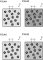
- FIGS. 4A, 4B, 4C, and 4D are explanatory diagrams of the first to fourth resin layers of the first arrangement.
- FIG. 4A is an enlarged schematic cross-sectional view of a part of the first resin layer, that is, the first fixing resin layer 14.
- FIG. 4B is an enlarged schematic cross-sectional view of a part of the second resin layer, that is, the inter-wire resin layer 16.
- FIG. 4C is an enlarged schematic cross-sectional view of a part of the third resin layer, that is, the second fixing resin layer 18.
- FIG. 4D is an enlarged schematic cross-sectional view of a part of the fourth resin layer, that is, the coating resin layer 20.
- the first fixing resin layer 14 includes a plurality of first particles 14a and first resin 14x.
- the first resin 14x surrounds the first particles 14a.
- the first particles 14a are so-called filler.
- the first resin 14x is, for example, thermoplastic resin.
- the first resin 14x is, for example, phenoxy resin.
- Material of the first resin 14x can be identified by, for example, a Fourier transform infrared spectrometer (FT-IR).
- FT-IR Fourier transform infrared spectrometer
- the first particles 14a are inorganic.
- the first particles 14a include, for example, at least one inorganic substance selected from a group including silica, alumina, silicon nitride, and alumina nitride.
- the at least one inorganic substance occupies 90% or more of volume of the first particles 14a.
- a chemical composition of the first particles 14a can be determined by, for example, identifying crystal by an X-ray diffraction method. In a case where the first particles 14a have poor crystallinity, the chemical composition of the first particles 14a can be measured by observing a cross section of the first fixing resin layer 14 with a scanning electron microscope (SEM), and performing an elemental analysis with an energy dispersive X-ray spectroscopy (EDS).
- SEM scanning electron microscope
- EDS energy dispersive X-ray spectroscopy
- a median particle diameter of the first particles 14a is, for example, 1 ⁇ m or more and 10 ⁇ m or less.
- the median particle diameter of the first particles 14a can be obtained from, for example, major axes of the plurality of first particles 14a which are measured with an image acquired by the SEM (an SEM image).
- a shape of the first particles 14a is, for example, but not particularly limited to, a plate shape, a spherical shape, a bale shape, a spheroidal shape, a columnar shape, a fibrous shape, or an irregular shape.
- FIG. 4A exemplifies a case where the first particles 14a have a spherical shape.
- Occupancy ratio of the first particles 14a in the first fixing resin layer 14 is, for example, 20% or more and 80% or less.
- the occupancy ratio of the first particles 14a in the first fixing resin layer 14 is represented by, for example, a proportion of the first particles 14a occupying an area observed in the SEM image.
- the occupancy ratio of the first particles 14a can be obtained by, for example, an image analysis of the SEM image.
- the inter-wire resin layer 16 includes a plurality of second particles 16a and second resin 16x.
- the second resin 16x surrounds the second particles 16a.
- the second particles 16a are so-called filler.
- Material of the second resin 16x is different from material of the first resin 14x.
- a chemical composition of the second resin 16x may be different from a chemical composition of the first resin 14x.
- the second resin 16x is, for example, thermo-setting resin.
- the second resin 16x is, for example, epoxy resin, phenol resin, unsaturated polyester resin, silicone resin, urethane resin, urea resin, polyimide resin, or a melamine resin.
- the second particles 16a are inorganic.
- the second particles 16a include, for example, at least one inorganic substance selected from a group including silica, alumina, silicon nitride, and alumina nitride.
- the at least one inorganic substance occupies 90% or more of volume of the second particles 16a.
- a median particle diameter of the second particles 16a is, for example, 1 ⁇ m or more and 10 ⁇ m or less.
- a shape of the second particles 16a is, for example, but not particularly limited to, a plate shape, a spherical shape, a bale shape, a spheroidal shape, a columnar shape, a fibrous shape, or an irregular shape.
- FIG. 4B exemplifies a case where the second particles 16a have a spherical shape.
- Occupancy ratio of the second particles 16a in the inter-wire resin layer 16 is, for example, 20% or more and 80% or less.
- the second fixing resin layer 18 includes a plurality of third particles 18a and third resin 18x.
- the third resin 18x surrounds the third particles 18a.
- the third particles 18a are so-called filler.
- Material of the third resin 18x is different from material of the second resin 16x.
- the third resin 18x is, for example, thermoplastic resin. Material of the third resin 18x is identical to material of the first resin 14x, for example. Glass transition temperature (Tg) of the third resin 18x is, for example, 200° C or lower.
- the third resin 18x is, for example, phenoxy resin.
- the third particles 18a are inorganic.
- the third particles 18a include, for example, at least one inorganic substance selected from a group including silica, alumina, silicon nitride, and alumina nitride.
- the at least one inorganic substance occupies 90% or more of volume of the third particles 18a.
- Material of the third particles 18a is identical to material of the first particles 14a, for example.
- a median particle diameter of the third particles 18a is, for example, 1 ⁇ m or more and 10 ⁇ m or less.
- a shape of the third particles 18a is, for example, but not particularly limited to, a plate shape, a spherical shape, a bale shape, a spheroidal shape, a columnar shape, a fibrous shape, or an irregular shape.
- FIG. 4C exemplifies a case where the third particles 18a have a spherical shape.
- Occupancy ratio of the third particles 18a in the second fixing resin layer 18 is, for example, 20% or more and 80% or less.
- the coating resin layer 20 includes a plurality of fourth particles 20a and fourth resin 20x.
- the fourth resin 20x surrounds the fourth particles 20a.
- the fourth particles 20a are so-called filler.
- Material of the fourth resin 20x is different from material of the first resin 14x.
- the fourth resin 20x is, for example, thermoplastic resin.
- the fourth resin 20x is, for example, polyvinyl formal resin, polyvinyl fluoride resin, saturated polyester resin, or polyurethane resin.
- the fourth particles 20a are inorganic.
- the fourth particles 20a include, for example, at least one inorganic substance selected from a group including silica, alumina, silicon nitride, and alumina nitride.
- the at least one inorganic substance occupies 90% or more of volume of the fourth particles 20a.
- a median particle diameter of the fourth particles 20a is, for example, 1 ⁇ m or more and 10 ⁇ m or less.
- a shape of the fourth particles 20a is, for example, but not particularly limited to, a plate shape, a spherical shape, a bale shape, a spheroidal shape, a columnar shape, a fibrous shape, or an irregular shape.
- FIG. 4D exemplifies a case where the fourth particles 20a have a spherical shape.
- FIGS. 5, 6 , 7 , and 8 are schematic diagrams illustrating a method for manufacturing the superconducting coil of the first arrangement.
- FIGS. 5, 6 , 7 , and 8 illustrate a cross section corresponding to FIG. 2 .
- the insulating substrate 10 is prepared ( FIG. 5 ) .
- the second fixing resin layer 18 is applied to the insulating substrate 10 ( FIG. 6 ).
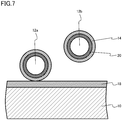
- the superconducting wire 12 is disposed on a surface of the second fixing resin layer 18 of the insulating substrate 10 ( FIG. 7 ).
- the superconducting wire 12 is wound such that a second region 12b of the superconducting wire 12 is disposed on the surface of the second fixing resin layer 18 so as to be substantially parallel to an adjacent first region 12a of the superconducting wire 12 previously disposed ( FIG. 8 ).
- the coating resin layer 20 is formed on the superconducting wire 12 in advance.
- the superconducting wire 12 on which the coating resin layer 20 is formed is passed through a tank filled with the first particles 14a and the first resin 14x to form the first fixing resin layer 14 of the coating resin layer 20. Then, the superconducting wire 12 is fixed to the surface of the second fixing resin layer 18 while, for example, the first fixing resin layer 14 is partially being softened by heat generated by ultrasonic irradiation.
- the inter-wire resin layer 16 is applied to the superconducting wire 12. Because the superconducting wire 12 is fixed to the insulating substrate 10 with the first fixing resin layer 14 and the second fixing resin layer 18, a position of the superconducting wire 12 is less likely to shift when the inter-wire resin layer 16 is applied.
- the superconducting wire 12 is fixed to the insulating substrate 10 by the inter-wire resin layer 16 being thermally set.
- the superconducting coil 100 illustrated in FIGS. 1A and 1B is formed.
- inorganic filler is added to the impregnated resin.
- inorganic filler difference in coefficient of thermal expansion between the metal included in the superconducting wire and the impregnated resin is reduced, and the difference in thermal shrinkage is reduced. Reduction of the difference in thermal shrinkage between the metal included in the superconducting wire and the impregnated resin reduces strain energy accumulated during cooling of the superconducting coil. Therefore, cracking is less likely to occur, and occurrence of quenching is suppressed.
- inclusion of filler in the impregnated resin increases fracture toughness of the impregnated resin. Even if strain energy accumulates, the increased fracture toughness of the impregnated resin reduces occurrence of cracking, and occurrence of quenching is suppressed.
- FIG. 9 is an enlarged schematic cross-sectional view illustrating a superconducting coil of a comparative example of the first arrangement.
- a superconducting coil 900 of the comparative example is a so-called saddle type coil.
- the superconducting coil 900 of the comparative example includes, as similar to the superconducting coil of the first arrangement, an insulating substrate 10, a superconducting wire 12, a first fixing resin layer 14, an inter-wire resin layer 16, a second fixing resin layer 18, and a coating resin layer 20.
- FIGS. 10A, 10B, 10C, and 10D are explanatory diagrams of a first to fourth resin layers of the comparative example of the first arrangement.
- FIG. 10A is an enlarged schematic cross-sectional view of a part of the first fixing resin layer 14.
- FIG. 10B is an enlarged schematic cross-sectional view of a part of the inter-wire resin layer 16.
- FIG. 10C is an enlarged schematic cross-sectional view of a part of the second fixing resin layer 18.
- FIG. 10D is an enlarged schematic cross-sectional view of a part of the coating resin layer 20.
- the superconducting coil 900 of the comparative example is different from the superconducting coil 100 of the first arrangement in that the first fixing resin layer 14, the second fixing resin layer 18, and the coating resin layer 20 do not include filler.
- the first fixing resin layer 14, the second fixing resin layer 18 and the coating resin layer 20 do not include filler. Therefore, when the superconducting coil 900 is cooled, the first fixing resin layer 14, the second fixing resin layer 18, and the coating resin layer 20 are likely to be subjected to cracking due to difference in coefficient of thermal expansion between the first fixing resin layer 14, the second fixing resin layer 18, or the coating resin layer 20, and the metal matrix 12y included in the superconducting wire 12.
- non-inclusion of filler causes insufficient fracture toughness of the first fixing resin layer 14, the second fixing resin layer 18, and the coating resin layer 20, cracking is likely to occur.
- quenching is likely to occur due to occurrence of cracking in the first fixing resin layer 14, the second fixing resin layer 18, or the coating resin layer 20.
- the first fixing resin layer 14 and the coating resin layer 20 are closer to the superconducting wire 12 than the inter-wire resin layer 16 is. Therefore, if cracking occurs in the first fixing resin layer 14 or the coating resin layer 20, quenching is more likely to occur.
- the first fixing resin layer 14, the second fixing resin layer 18 and the coating resin layer 20 include filler. Therefore, the difference in coefficient of thermal expansion between the first fixing resin layer 14, the second fixing resin layer 18, or the coating resin layer 20, and the metal matrix 12y included in the superconducting wire 12 is small, as compared to a case of the superconducting coil 900 of the comparative example. Further, fracture toughness of the first fixing resin layer 14, the second fixing resin layer 18, and the coating resin layer 20 is high, as compared to a case of the superconducting coil 900 of the comparative example.
- a superconducting coil in which occurrence of quenching is suppressed can be implemented.
- a superconducting coil of a second arrangement is different from the superconducting coil of the first arrangement in that a fourth resin layer does not include fourth particles.
- a part of description of content overlapping content of the first arrangement will be omitted.
- FIGS. 11A, 11B, 11C, and 11D are explanatory diagrams of first to fourth resin layers of the second arrangement.
- FIG. 11A is an enlarged schematic cross-sectional view of a part of the first resin layer, that is, a first fixing resin layer 14.
- FIG. 11B is an enlarged schematic cross-sectional view of a part of the second resin layer, that is, an inter-wire resin layer 16.
- FIG. 11C is an enlarged schematic cross-sectional view of a part of the third resin layer, that is, a second fixing resin layer 18.
- FIG. 11D is an enlarged schematic cross-sectional view of a part of the fourth resin layer, that is, a coating resin layer 20.
- the coating resin layer 20 does not include filler.
- the first fixing resin layer 14 and the second fixing resin layer 18 include filler. Therefore, as compared to a case of the superconducting coil 900 of the comparative example, occurrence of cracking is suppressed in the first fixing resin layer 14 and the second fixing resin layer 18, and occurrence of quenching is suppressed.
- a superconducting coil in which occurrence of quenching is suppressed can be implemented.
- a superconducting coil of a third arrangement is different from the superconducting coil of the first arrangement in that particle diameter distribution of first particles is bimodal.
- a part of description of content overlapping content of the first arrangement will be omitted.
- FIGS. 12A, 12B, 12C, and 12D are explanatory diagrams of first to fourth resin layers of the third arrangement.
- FIG. 12A is an enlarged schematic cross-sectional view of a part of the first resin layer, that is, a first fixing resin layer 14.
- FIG. 12B is an enlarged schematic cross-sectional view of a part of the second resin layer, that is, an inter-wire resin layer 16.
- FIG. 12C is an enlarged schematic cross-sectional view of a part of the third resin layer, that is, a second fixing resin layer 18.
- FIG. 12D is an enlarged schematic cross-sectional view of a part of the fourth resin layer, that is, a coating resin layer 20.
- a plurality of first particles 14a included in the first fixing resin layer 14 include a large-sized particle and a small-sized particle. Particle diameter distribution of the first particles 14a is bimodal.
- Whether or not the particle diameter distribution of the first particles 14a is bimodal can be determined by measuring major axes of the first particles 14a with an SEM image, and obtaining frequency distribution of the major axes of the first particles 14a.
- a particle diameter indicating a first peak is, for example, 1 ⁇ m or more and 10 ⁇ m or less
- a particle diameter indicating a second peak is, for example, 10 ⁇ m or more and 50 ⁇ m or less.
- a plurality of third particles 18a included in the second fixing resin layer 18 include a large-sized particle and a small-sized particle. Particle diameter distribution of the third particles 18a is bimodal.
- a superconducting coil in which occurrence of quenching is further suppressed can be implemented.
- a superconducting coil of a fourth arrangement is different from the superconducting coil of the first arrangement in that a median particle diameter of first particles is smaller than a median particle diameter of second particles.
- a part of description of content overlapping content of the first arrangement will be omitted.
- FIGS. 13A, 13B, 13C, and 13D are explanatory diagrams of first to fourth resin layers of the fourth arrangement.
- FIG. 13A is an enlarged schematic cross-sectional view of a part of the first resin layer, that is, a first fixing resin layer 14.
- FIG. 13B is an enlarged schematic cross-sectional view of a part of the second resin layer, that is, an inter-wire resin layer 16.
- FIG. 13C is an enlarged schematic cross-sectional view of a part of the third resin layer, that is, a second fixing resin layer 18.
- FIG. 13D is an enlarged schematic cross-sectional view of a part of the fourth resin layer, that is, a coating resin layer 20.
- a particle diameter of a plurality of first particles 14a included in the first fixing resin layer 14 is smaller than a particle diameter of a plurality of second particles 16a included in the inter-wire resin layer 16. Therefore, a median particle diameter of the first particles 14a is smaller than a median particle diameter of the second particles 16a.
- the fracture toughness of the inter-wire resin layer 16 is low, cracking is more likely to occur in the inter-wire resin layer 16, which is farther from a superconducting wire 12 than the first fixing resin layer 14 is. In other words, cracking is less likely to occur in the first fixing resin layer 14, which is closer to the superconducting wire 12.
- a superconducting coil in which occurrence of quenching is further suppressed can be implemented.
- a superconducting coil of a fifth arrangement is different from the superconducting coil of the first arrangement in that occupancy ratio of first particles in a first resin layer is higher than occupancy ratio of second particles in a second resin layer.
- occupancy ratio of first particles in a first resin layer is higher than occupancy ratio of second particles in a second resin layer.
- FIGS. 14A, 14B, 14C, and 14D are explanatory diagrams of first to fourth resin layers of the fifth arrangement.
- FIG. 14A is an enlarged schematic cross-sectional view of a part of the first resin layer, that is, a first fixing resin layer 14.
- FIG. 14B is an enlarged schematic cross-sectional view of a part of the second resin layer, that is, an inter-wire resin layer 16.
- FIG. 14C is an enlarged schematic cross-sectional view of a part of the third resin layer, that is, a second fixing resin layer 18.
- FIG. 14D is an enlarged schematic cross-sectional view of a part of the fourth resin layer, that is, a coating resin layer 20.
- occupancy ratio of a plurality of first particles 14a included in the first fixing resin layer 14 is higher than occupancy ratio of a plurality of second particles 16a included in the inter-wire resin layer 16.
- the fracture toughness of the inter-wire resin layer 16 is low, cracking is more likely to occur in the inter-wire resin layer 16, which is farther from a superconducting wire 12 than the first fixing resin layer 14 is. In other words, cracking is less likely to occur in the first fixing resin layer 14, which is closer to the superconducting wire 12.
- a superconducting coil in which occurrence of quenching is further suppressed can be implemented.
- a superconducting coil of a sixth arrangement is different from the superconducting coil of the first arrangement in that second particles include crystal having cleavage.
- second particles include crystal having cleavage.
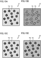
- FIGS. 15A, 15B, 15C, and 15D are explanatory diagrams of first to fourth resin layers of the sixth arrangement.
- FIG. 15A is an enlarged schematic cross-sectional view of a part of the first resin layer, that is, a first fixing resin layer 14.
- FIG. 15B is an enlarged schematic cross-sectional view of a part of the second resin layer, that is, an inter-wire resin layer 16.
- FIG. 15C is an enlarged schematic cross-sectional view of a part of the third resin layer, that is, a second fixing resin layer 18.
- FIG. 15D is an enlarged schematic cross-sectional view of a part of the fourth resin layer, that is, a coating resin layer 20.
- a plurality of second particles 16a included in the inter-wire resin layer 16 include crystal having cleavage.
- the second particles 16a have volume resistivity of 10 -2 ⁇ m or more and include crystal having cleavage.
- the crystal is a main component of the second particles 16a.
- the crystal occupies 90% or more of volume of the second particles 16a.
- the second particles 16a are, for example, the crystal itself.
- Cleavage is a property of crystal tending to break parallel to a specific crystal plane. Cleavage is classified as perfect, good, distinct, or indistinct, depending on a degree.
- the second particles 16a have, for example, perfect or distinct cleavage.
- Volume resistivity and cleavage are physical properties unique to crystal. If the crystal included in the second particles 16a is identified, volume resistivity and cleavage of the crystal can be determined. The crystal included in the second particles 16a can be identified by, for example, a powder X-ray diffraction method.
- the crystal included in the second particles 16a is, for example, at least either of phyllosilicate mineral or hexagonal boron nitride.
- Volume resistivity of the phyllosilicate mineral or the hexagonal boron nitride is, for example, 10 -2 ⁇ m or more and 10 15 ⁇ m or less. Further, the phyllosilicate mineral or the hexagonal boron nitride has cleavage.
- the phyllosilicate mineral has a sheet structure formed by a two-dimensionally spread SiO 2 tetrahedra.
- the phyllosilicate mineral is plate-shaped or flake-shaped and has perfect or distinct cleavage parallel to a bottom surface.
- the phyllosilicate mineral included in the second particles 16a is, for example, at least one of mineral belonging to the mica group, clay mineral, pyrophyllite, or talc.
- the mineral belonging to the mica group is, for example, muscovite, phlogopite or biotite.
- the clay mineral is, for example, kaolinite or montmorillonite.
- a shape of the second particles 16a is, for example, but not particularly limited to, a plate shape, a spherical shape, a bale shape, a spheroidal shape, a columnar shape, a fibrous shape, or an irregular shape.
- FIG. 15B exemplifies a case where the second particles 16a have a plate shape.
- Crystal having cleavage breaks by relatively little stress. Therefore, because the second particles 16a include crystal having cleavage, fracture toughness of the inter-wire resin layer 16 is lower than the fracture toughness of the inter-wire resin layer 16 of the first arrangement.
- the fracture toughness of the inter-wire resin layer 16 is low, cracking is more likely to occur in the inter-wire resin layer 16, which is farther from a superconducting wire 12 than the first fixing resin layer 14 is. In other words, cracking is less likely to occur in the first fixing resin layer 14, which is closer to the superconducting wire 12.
- the second particles 16a have volume resistivity of 10 -2 ⁇ m or more, and therefore insulation between portions of the superconducting wire 12 is secured.
- a superconducting coil in which occurrence of quenching is further suppressed can be implemented.
- a superconducting coil of a seventh arrangement is different from the superconducting coil of the sixth arrangement in that second particles include a spherical particle.
- second particles include a spherical particle.
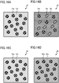
- FIGS. 16A, 16B, 16C, and 16D are explanatory diagrams of first to fourth resin layers of the seventh arrangement.
- FIG. 16A is an enlarged schematic cross-sectional view of a part of the first resin layer, that is, a first fixing resin layer 14.
- FIG. 16B is an enlarged schematic cross-sectional view of a part of the second resin layer, that is, an inter-wire resin layer 16.
- FIG. 16C is an enlarged schematic cross-sectional view of a part of the third resin layer, that is, a second fixing resin layer 18.
- FIG. 16D is an enlarged schematic cross-sectional view of a part of the fourth resin layer, that is, a coating resin layer 20.
- a plurality of second particles 16a included in the inter-wire resin layer 16 include crystal having cleavage and a spherical particle.
- the second particles 16a include a spherical particle, fracture toughness is higher, as compared to a case where crystal having cleavage alone is included. Therefore, as compared to a case of the superconducting coil of the sixth arrangement, occurrence of quenching is further suppressed.
- a superconducting coil in which occurrence of quenching is further suppressed can be implemented.
- a superconducting coil of an eighth arrangement is different from the superconducting coil of the first arrangement in having an irregular shape.
- a part of description of content overlapping content of the first arrangement will be omitted.
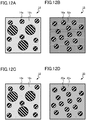
- FIGS. 17A, 17B, 17C, and 17D are explanatory diagrams of first to fourth resin layers of the eighth arrangement.
- FIG. 17A is an enlarged schematic cross-sectional view of a part of the first resin layer, that is, a first fixing resin layer 14.
- FIG. 17B is an enlarged schematic cross-sectional view of a part of the second resin layer, that is, an inter-wire resin layer 16.
- FIG. 17C is an enlarged schematic cross-sectional view of a part of the third resin layer, that is, a second fixing resin layer 18.
- FIG. 17D is an enlarged schematic cross-sectional view of a part of the fourth resin layer, that is, a coating resin layer 20.
- a plurality of second particles 16a included in the inter-wire resin layer 16 have an irregular shape.
- the second particles 16a are, for example, crushed silica.
- a particle having an irregular shape breaks by relatively little stress, as compared to a spherical particle, for example. Therefore, because the second particles 16a have an irregular shape, fracture toughness of the inter-wire resin layer 16 is lower than the fracture toughness of the inter-wire resin layer 16 of the first arrangement.
- the fracture toughness of the inter-wire resin layer 16 is low, cracking is more likely to occur in the inter-wire resin layer 16, which is farther from a superconducting wire 12 than the first fixing resin layer 14 is. In other words, cracking is less likely to occur in the first fixing resin layer 14, which is closer to the superconducting wire 12.
- a superconducting coil in which occurrence of quenching is further suppressed can be implemented.
- a superconducting coil of a ninth arrangement includes a winding frame, a superconducting wire wound on the winding frame, the superconducting wire having a first region and a second region facing the first region, a first resin layer surrounding the superconducting wire and including a plurality of first particles and first resin surrounding the first particles, and a second resin layer positioned between the first region and the second region, the second resin layer covering the first resin layer and including a plurality of second particles and second resin surrounding the second particles and being made of material different from material of the first resin.
- FIG. 18 is a schematic perspective view illustrating the superconducting coil of the ninth arrangement.
- FIG. 19 is a schematic cross-sectional view illustrating the superconducting coil of the ninth arrangement.
- a superconducting coil 200 of the ninth arrangement is used as a coil for, for example, magnetic field generation of a superconducting device, such as an NMR, an MRI, heavy particle therapy equipment, or a superconducting magnetic levitation railway vehicle.
- the superconducting coil 200 of the ninth arrangement is a so-called solenoid coil.
- the superconducting coil 200 includes a winding frame 30, an inner peripheral insulation layer 31a, an upper insulation layer 31b, a lower insulation layer 31c, and a winding unit 32.
- the winding unit 32 includes a superconducting wire 40, a coating resin layer 42, and an inter-wire resin layer 44.
- the coating resin layer 42 is an example of the first resin layer.
- the inter-wire resin layer 44 is an example of the second resin layer.
- the inner peripheral insulation layer 31a, the upper insulation layer 31b, and the lower insulation layer 31c are formed of, for example, fiber-reinforced plastic.
- the inner peripheral insulation layer 31a, the upper insulation layer 31b, and the lower insulation layer 31c have a function of insulating the winding unit 32 from the winding frame 30 or an outside.
- the superconducting wire 40 is linear shape, for example.
- the superconducting wire 40 is wound on the winding frame 30 in a solenoid shape around a winding center C.
- FIG. 20 is a schematic cross-sectional view illustrating a superconducting wire of the ninth arrangement.
- a cross section of the superconducting wire 40 is, for example, rectangular.
- the superconducting wire 40 includes superconducting materials 40x and a metal matrix 40y.
- the superconducting wire 40 has a structure in which a plurality of superconducting materials 40x are disposed in the metal matrix 40y.
- the superconducting material 40x is, for example, a low-temperature superconducting material having a critical temperature Tc of 8 K or higher and 40 K or lower.
- the superconducting material 12x is, for example, a niobium-titanium alloy-based, niobium-tin compound-based, niobium-aluminum compound-based, or magnesium diboride-based low-temperature superconducting material.
- the metal matrix 40y is metal.
- the metal matrix 40y is, for example, copper.
- FIG. 21 is an enlarged schematic cross-sectional view illustrating a part of a winding unit of the superconducting coil of the ninth arrangement.
- the superconducting wire 40 has a first region 40a and a second region 40b.
- the first region 40a and the second region 40b are regions disposed adjacent to each other in parallel.
- the coating resin layer 42 surrounds the superconducting wire 40.
- the coating resin layer 42 has a function of coating and protecting the superconducting wire 40. Thickness of the coating resin layer 42 is, for example, 30 ⁇ m or more and 100 ⁇ m or less.
- the inter-wire resin layer 44 is disposed between the first region 40a and second region 40b of the superconducting wire 40.
- the inter-wire resin layer 44 covers the coating resin layer 42.
- the inter-wire resin layer 44 is in contact with the coating resin layer 42.
- the inter-wire resin layer 44 surrounds the coating resin layer 42, for example.
- the inter-wire resin layer 44 has a function of inhibiting the superconducting wire 40 from moving by vibration generated during use of the superconducting coil 200 or by electromagnetic force on the superconducting wire, and from being quenched by voltage generation or frictional heat caused by coil deformation. Further, the inter-wire resin layer 44 has a function of providing insulation between portions of the superconducting wire 40.
- FIGS. 22A and 22B are explanatory diagrams of the first resin layer and the second resin layer of the ninth arrangement.
- FIG. 22A is an enlarged schematic cross-sectional view of a part of the first resin layer, that is, the coating resin layer 42.
- FIG. 22B is an enlarged schematic cross-sectional view of a part of the second resin layer, that is, the inter-wire resin layer 44.
- the coating resin layer 42 includes a plurality of first particles 42a and first resin 42x.
- the first resin 42x surrounds the first particles 42a.
- the first particles 42a are so-called filler.
- the first resin 42x is, for example, thermoplastic resin.
- the first resin 42x is, for example, polyvinyl formal resin.
- Material of the first resin 42x can be identified by, for example, an FT-IR.
- the first particles 42a are inorganic.
- the first particles 42a include, for example, at least one inorganic substance selected from a group including silica, alumina, silicon nitride, and alumina nitride.
- the at least one inorganic substance occupies 90% or more of volume of the first particles 42a.
- a chemical composition of the first particles 42a can be determined by, for example, identifying crystal by an X-ray diffraction method. In a case where the first particles 42a have poor crystallinity, the chemical composition of the first particles 42a can be measured by observing a cross section of the coating resin layer 42 with an SEM, and performing an elemental analysis with an EDS.
- a median particle diameter of the first particles 42a is, for example, 1 ⁇ m or more and 10 ⁇ m or less.
- the median particle diameter of the first particles 42a can be obtained from, for example, major axes of the plurality of first particles 42a which are measured with an image acquired by the SEM (an SEM image).
- a shape of the first particles 42a is, for example, but not particularly limited to, a plate shape, a spherical shape, a bale shape, a spheroidal shape, a columnar shape, a fibrous shape, or an irregular shape.
- FIG. 22A exemplifies a case where the first particles 42a have a spherical shape.
- Occupancy ratio of the first particles 42a in the coating resin layer 42 is, for example, 20% or more and 80% or less.
- the occupancy ratio of the first particles 42a in the coating resin layer 42 is represented by, for example, a proportion of the first particles 42a occupying an area observed in the SEM image.
- the occupancy ratio of the first particles 42a can be obtained by, for example, an image analysis of the SEM image.
- the inter-wire resin layer 44 includes a plurality of second particles 44a and second resin 44x.
- the second resin 44x surrounds the second particles 44a.
- the second particles 44a are so-called filler.
- Material of the second resin 44x is different from material of the first resin 42x.
- the second resin 44x is, for example, thermo-setting resin.
- the second resin 44x is, for example, epoxy resin.
- the second particles 44a are inorganic.
- the second particles 44a include, for example, at least one inorganic substance selected from a group including silica, alumina, silicon nitride, and alumina nitride.
- the at least one inorganic substance occupies 90% or more of volume of the second particles 44a.
- a median particle diameter of the second particles 44a is, for example, 1 ⁇ m or more and 10 ⁇ m or less.
- a shape of the second particles 44a is, for example, but not particularly limited to, a plate shape, a spherical shape, a bale shape, a spheroidal shape, a columnar shape, a fibrous shape, or an irregular shape.
- FIG. 22B exemplifies a case where the second particles 44a have a spherical shape.
- Occupancy ratio of the second particles 44a in the inter-wire resin layer 44 is, for example, 20% or more and 80% or less.
- the superconducting wire 40 coated by the coating resin layer 42 is wound on the winding frame 30 while the second resin 44x including the second particles 44a is being applied. Then, the inter-wire resin layer 44 is formed and a superconducting wire 12 is fixed by the second resin 44x being thermally set.
- inorganic filler is added to the impregnated resin.
- inorganic filler difference in coefficient of thermal expansion between the metal included in the superconducting wire and the impregnated resin is reduced, and the difference in thermal shrinkage is reduced. Reduction of the difference in thermal shrinkage between the metal included in the superconducting wire and the impregnated resin reduces strain energy accumulated during cooling of the superconducting coil. Therefore, cracking is less likely to occur, and occurrence of quenching is suppressed.
- inclusion of filler in the impregnated resin increases fracture toughness of the impregnated resin. Even if strain energy accumulates, the increased fracture toughness of the impregnated resin reduces occurrence of cracking, and occurrence of quenching is suppressed.
- FIG. 23 is an enlarged schematic cross-sectional view illustrating a superconducting coil of a comparative example of the ninth arrangement.
- a superconducting coil 1000 of the comparative example is a so-called solenoid coil.
- the superconducting coil 1000 of the comparative example includes a winding frame 30, an inner peripheral insulation layer 31a, an upper insulation layer 31b, a lower insulation layer 31c, and a winding unit 32.
- the winding unit 32 includes a superconducting wire 40, a coating resin layer 42, and an inter-wire resin layer 44.
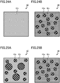
- FIGS. 24A and 24B are explanatory diagrams of first resin layer and second resin layer of the comparative example of the ninth arrangement.
- FIG. 24A is an enlarged schematic cross-sectional view of a part of the first resin layer, that is, the coating resin layer 42.
- FIG. 24B is an enlarged schematic cross-sectional view of a part of the second resin layer, that is, the inter-wire resin layer 44.
- the superconducting coil 1000 of the comparative example is different from the superconducting coil 200 of the ninth arrangement in that the coating resin layer 42 does not include filler.
- the coating resin layer 42 does not include filler. Therefore, when the superconducting coil 1000 is cooled, the coating resin layer 42 is likely to be subjected to cracking due to difference in coefficient of thermal expansion between the coating resin layer 42 and the metal matrix 40y included in the superconducting wire 40. Further, fracture toughness of the coating resin layer 42 is insufficient, and cracking is likely to occur.
- the superconducting coil 1000 of the comparative example is likely to be subjected to quenching caused by occurrence of cracking in the coating resin layer 42.
- the coating resin layer 42 is closer to the superconducting wire 40 than the inter-wire resin layer 44 is. Therefore, if cracking occurs in the coating resin layer 42, quenching is more likely to occur.
- the coating resin layer 42 includes filler. Therefore, the difference in coefficient of thermal expansion between the coating resin layer 42 and the metal matrix 40y included in the superconducting wire 40 is small, as compared to a case of the superconducting coil 1000 of the comparative example. Further, the fracture toughness of the coating resin layer 42 is high, as compared to a case of the superconducting coil 1000 of the comparative example. Therefore, as compared to a case of the superconducting coil 1000 of the comparative example, occurrence of cracking is suppressed in the coating resin layer 42, and occurrence of quenching is suppressed.
- a superconducting coil in which occurrence of quenching is suppressed can be implemented.
- a superconducting coil of a tenth arrangement is different from the superconducting coil of the ninth arrangement in that particle diameter distribution of first particles is bimodal.
- a part of description of content overlapping content of the ninth arrangement will be omitted.
- FIGS. 25A and 25B are explanatory diagrams of a first resin layer and second resin layer of the tenth arrangement.
- FIG. 25A is an enlarged schematic cross-sectional view of a part of the first resin layer, that is, a coating resin layer 42.
- FIG. 25B is an enlarged schematic cross-sectional view of a part of the second resin layer, that is, an inter-wire resin layer 44.
- a plurality of first particles 42a included in the coating resin layer 42 include a large-sized particle and a small-sized particle. Particle diameter distribution of the first particles 42a is bimodal.
- Whether or not the particle diameter distribution of the first particles 42a is bimodal can be determined by measuring major axes of the first particles 42a with an SEM image, and obtaining frequency distribution of the major axes of the first particles 42a.
- a particle diameter indicating a first peak is, for example, 1 ⁇ m or more and 10 ⁇ m or less
- a particle diameter indicating a second peak is, for example, 10 ⁇ m or more and 50 ⁇ m or less.
- a superconducting coil in which occurrence of quenching is further suppressed can be implemented.
- a superconducting coil of an eleventh arrangement is different from the superconducting coil of the ninth arrangement in that a median particle diameter of first particles is smaller than a median particle diameter of second particles.
- a part of description of content overlapping content of the ninth arrangement will be omitted.
- FIGS. 26A and 26B are explanatory diagrams of a first resin layer and second resin layer of the eleventh arrangement.
- FIG. 26A is an enlarged schematic cross-sectional view of a part of the first resin layer, that is, a coating resin layer 42.
- FIG. 26B is an enlarged schematic cross-sectional view of a part of the second resin layer, that is, an inter-wire resin layer 44.
- a particle diameter of a plurality of first particles 42a included in the coating resin layer 42 is smaller than a particle diameter of a plurality of second particles 44a included in the inter-wire resin layer 44. Therefore, a median particle diameter of the first particles 42a is smaller than a median particle diameter of the second particles 44a.
- the fracture toughness of the inter-wire resin layer 44 is low, cracking is more likely to occur in the inter-wire resin layer 44, which is farther from a superconducting wire 40 than the coating resin layer 42 is. In other words, cracking is less likely to occur in the coating resin layer 42, which is closer to the superconducting wire 40.
- a superconducting coil in which occurrence of quenching is further suppressed can be implemented.
- a superconducting coil of a twelfth arrangement is different from the superconducting coil of the ninth arrangement in that occupancy ratio of first particles in a first resin layer is higher than occupancy ratio of the second particles in a second resin layer.
- occupancy ratio of first particles in a first resin layer is higher than occupancy ratio of the second particles in a second resin layer.
- FIGS. 27A and 27B are explanatory diagrams of first resin layer and the second resin layer of the twelfth arrangement.
- FIG. 27A is an enlarged schematic cross-sectional view of a part of the first resin layer, that is, a coating resin layer 42.
- FIG. 27B is an enlarged schematic cross-sectional view of a part of the second resin layer, that is, an inter-wire resin layer 44.
- occupancy ratio of a plurality of first particles 42a included in the coating resin layer 42 is higher than occupancy ratio of a plurality of second particles 44a included in the inter-wire resin layer 44.
- the fracture toughness of the inter-wire resin layer 44 is low, cracking is more likely to occur in the inter-wire resin layer 44, which is farther from a superconducting wire 40 than the coating resin layer 42 is. In other words, cracking is less likely to occur in the coating resin layer 42, which is closer to the superconducting wire 40.
- a superconducting coil in which occurrence of quenching is further suppressed can be implemented.
- a superconducting coil of a thirteenth arrangement is different from the superconducting coil of the ninth arrangement in that second particles include crystal having cleavage.
- second particles include crystal having cleavage.
- FIGS. 28A and 28B are explanatory diagrams of a first resin layer and second resin layer of the thirteenth arrangement.
- FIG. 28A is an enlarged schematic cross-sectional view of a part of the first resin layer, that is, a coating resin layer 42.
- FIG. 28B is an enlarged schematic cross-sectional view of a part of the second resin layer, that is, an inter-wire resin layer 44.
- a plurality of second particles 44a included in the inter-wire resin layer 44 include crystal having cleavage.
- the second particles 44a have volume resistivity of 10 -2 ⁇ m or more and include crystal having cleavage.
- the crystal is a main component of the second particles 44a.
- the crystal occupies 90% or more of volume of the second particles 44a.
- the second particles 44a are, for example, the crystal itself.
- Cleavage is a property of crystal tending to break parallel to a specific crystal plane. Cleavage is classified as perfect, good, distinct, or indistinct, depending on a degree.
- the second particles 44a have, for example, perfect or distinct cleavage.
- Volume resistivity and cleavage are physical properties unique to crystal. If the crystal included in the second particles 44a is identified, volume resistivity and cleavage of the crystal can be determined. The crystal included in the second particles 44a can be identified by, for example, a powder X-ray diffraction method.
- the crystal included in the second particles 44a is, for example, at least either of phyllosilicate mineral or hexagonal boron nitride.
- Volume resistivity of the phyllosilicate mineral or the hexagonal boron nitride is, for example, 10 -2 ⁇ m or more and 10 15 ⁇ m or less. Further, the phyllosilicate mineral or the hexagonal boron nitride has cleavage.
- the phyllosilicate mineral has a sheet structure formed by a two-dimensionally spread SiO 2 tetrahedra.
- the phyllosilicate mineral is plate-shaped or flake-shaped and has perfect or distinct cleavage parallel to a bottom surface.
- the phyllosilicate mineral included in the second particles 44a is, for example, at least one of mineral belonging to the mica group, clay mineral, pyrophyllite, or talc.
- the mineral belonging to the mica group is, for example, muscovite, phlogopite or biotite.
- the clay mineral is, for example, kaolinite or montmorillonite.
- a shape of the second particles 44a is, for example, but not particularly limited to, a plate shape, a spherical shape, a bale shape, a spheroidal shape, a columnar shape, a fibrous shape, or an irregular shape.
- FIG. 28B exemplifies a case where the second particles 44a have a plate shape.
- Crystal having cleavage breaks by relatively little stress. Therefore, because the second particles 44a include crystal having cleavage, fracture toughness of the inter-wire resin layer 44 is lower than the fracture toughness of the inter-wire resin layer 44 of the ninth arrangement.
- the fracture toughness of the inter-wire resin layer 44 is low, cracking is more likely to occur in the inter-wire resin layer 44, which is farther from a superconducting wire 40 than the coating resin layer 42 is. In other words, cracking is less likely to occur in the coating resin layer 42, which is closer to the superconducting wire 40.
- the second particles 44a have volume resistivity of 10 -2 ⁇ m or more, and therefore insulation between portions of the superconducting wire 40 is secured.
- a superconducting coil in which occurrence of quenching is further suppressed can be implemented.
- a superconducting coil of a fourteenth arrangement is different from the superconducting coil of the ninth arrangement in having an irregular shape.
- a part of description of content overlapping content of the ninth arrangement will be omitted.
- FIGS. 29A and 29B are explanatory diagrams of a first resin layer and second resin layer of the fourteenth arrangement.
- FIG. 29A is an enlarged schematic cross-sectional view of a part of the first resin layer, that is, a coating resin layer 42.
- FIG. 29B is an enlarged schematic cross-sectional view of a part of the second resin layer, that is, an inter-wire resin layer 44.
- a plurality of second particles 44a included in the inter-wire resin layer 44 have an irregular shape.
- the second particles 44a are, for example, crushed silica.
- a particle having an irregular shape breaks by relatively little stress, as compared to a spherical particle, for example. Therefore, because the second particles 44a have an irregular shape, fracture toughness of the inter-wire resin layer 44 is lower than the fracture toughness of the inter-wire resin layer 44 of the ninth arrangement.
- the fracture toughness of the inter-wire resin layer 44 is low, cracking is more likely to occur in the inter-wire resin layer 44, which is farther from a superconducting wire 40 than the coating resin layer 42 is. In other words, cracking is less likely to occur in the coating resin layer 42, which is closer to the superconducting wire 40.
- a superconducting coil in which occurrence of quenching is further suppressed can be implemented.
- a superconducting device of a fifteenth arrangement includes a superconducting coil of the first to fourteenth arrangements.
- a part of description of content overlapping content of the first to fourteenth arrangements will be omitted.
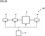
- FIG. 30 is a block diagram illustrating the superconducting device of the fifteenth arrangement.
- the superconducting device of the fifteenth arrangement is heavy particle therapy equipment 300.
- the heavy particle therapy equipment 300 is an example of a superconducting device.
- the heavy particle therapy equipment 300 includes an injection system 50, a synchrotron accelerator 52, a beam transportation system 54, an irradiation system 56, and a control system 58.
- the injection system 50 has a function of generating a carbon ion used for treatment and performing pre-acceleration to inject the carbon ion into the synchrotron accelerator 52.
- the injection system 50 has, for example, an ion generation source and a linear accelerator.
- the synchrotron accelerator 52 has a function of accelerating a carbon ion beam injected from the injection system 50 to energy suitable for treatment.
- the synchrotron accelerator 52 uses a superconducting coil of the first to fourteenth arrangements.
- the beam transportation system 54 has a function of transporting the carbon ion beam injected from the synchrotron accelerator 52 to the irradiation system 56.
- the beam transportation system 54 has, for example, a bending electromagnet.
- the irradiation system 56 includes a function of irradiating the carbon ion beam injected from the beam transportation system 54 to a patient as an irradiation object.
- the irradiation system 56 has, for example, a rotary gantry that allows irradiation of a carbon ion beam from any direction.
- the rotary gantry uses a superconducting coil of the first to fourteenth arrangements.
- the control system 58 controls the injection system 50, the synchrotron accelerator 52, the beam transportation system 54, and the irradiation system 56.
- the control system 58 is, for example, a computer.
- the synchrotron accelerator 52 and the rotary gantry use a superconducting coil of the first to fourteenth arrangements. Therefore, occurrence of quenching is suppressed, and high reliability is achieved.
- the heavy particle therapy equipment 300 is described as an example of the superconducting device.
- the superconducting device may be an NMR, an MRI, or a superconducting magnetic levitation railway vehicle.
- a superconducting wire rod for superconducting coil of a sixteenth arrangement includes a superconducting wire and a resin layer that coats the superconducting wire and includes particles and resin surrounding the particles.
- a superconducting wire rod 400 of the sixteenth arrangement is linear shape, for example. By being wound on a surface of an insulating substrate in a three-dimensional shape, for example, the superconducting wire rod 400 forms a saddle-type superconducting coil. By being wound on a winding frame, for example, the superconducting wire rod 400 forms a solenoid superconducting coil.
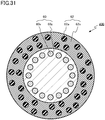
- FIG. 31 is a schematic cross-sectional view illustrating a superconducting wire rod of the sixteenth arrangement.
- a cross section of the superconducting wire rod 400 is, for example, circular.
- a diameter of the superconducting wire rod 400 is, for example, 0.5 mm or more and 2 mm or less.
- the superconducting wire rod 400 includes a superconducting wire 60 and a coating resin layer 62.
- the coating resin layer 62 is an example of a resin layer.
- the superconducting wire 60 includes superconducting materials 60x and a metal matrix 60y.
- the superconducting wire 60 has a structure in which a plurality of superconducting materials 60x are disposed in the metal matrix 60y.
- the superconducting material 60x is, for example, a low-temperature superconducting material having a critical temperature Tc of 8 K or higher and 40 K or lower.
- the superconducting material 60x is, for example, a niobium-titanium alloy-based, niobium-tin compound-based, niobium-aluminum compound-based, or magnesium diboride-based low-temperature superconducting material.
- the metal matrix 60y is metal.
- the metal matrix 60y is, for example, copper.
- the coating resin layer 62 coats the superconducting wire 60.
- the coating resin layer 62 is in contact with the superconducting wire 60.
- the coating resin layer 62 has a function of coating and protecting the superconducting wire 60. Thickness of the coating resin layer 62 is, for example, 30 ⁇ m or more and 100 ⁇ m or less.
- the coating resin layer 62 includes particles 62a and resin 62x.
- the resin 62x surrounds the particles 62a.
- the particles 62a are so-called filler.
- the resin 62x is, for example, thermoplastic resin.
- the resin 62x is, for example, polyvinyl formal resin.
- Material of the resin 62x can be identified by, for example, an FT-IR.
- the particles 62a are inorganic.
- the particles 62a include, for example, at least one inorganic substance selected from a group including silica, alumina, silicon nitride, and alumina nitride.
- the at least one inorganic substance occupies 90% or more of volume of the first particles 42a.
- a chemical composition of the particles 62a can be determined by, for example, identifying crystal by an X-ray diffraction method. In a case where the particles 62a have poor crystallinity, the chemical composition of first particles 14a can be measured by observing a cross section of the coating resin layer 62 with an SEM, and performing an elemental analysis with an EDS.
- a median particle diameter of the particles 62a is, for example, 1 ⁇ m or more and 10 ⁇ m or less.
- the median particle diameter of the particles 62a can be obtained from, for example, major axes of a plurality of particles 62a which are measured with an image acquired by the SEM (an SEM image) .
- a shape of the particles 62a is, for example, but not particularly limited to, a plate shape, a spherical shape, a bale shape, a spheroidal shape, a columnar shape, a fibrous shape, or an irregular shape.
- FIG. 31 exemplifies a case where the particles 62a have a spherical shape.
- Occupancy ratio of the particles 62a in the coating resin layer 62 is, for example, 20% or more and 80% or less.
- the occupancy ratio of the particles 62a in the coating resin layer 62 is represented by, for example, a proportion of the particles 62a occupying an area observed in the SEM image.
- the occupancy ratio of the particles 62a can be obtained by, for example, an image analysis of the SEM image.
- the coating resin layer 62 includes filler. Therefore, difference in coefficient of thermal expansion between the coating resin layer 62 and the metal matrix 60y included in the superconducting wire 60 is small, as compared to a case where the coating resin layer 62 does not include filler. Further, fracture toughness of the coating resin layer 62 is high, as compared to a case where the coating resin layer 62 does not include filler. Therefore, in a case where the superconducting wire rod 400 is applied to a superconducting coil, occurrence of cracking is suppressed in the coating resin layer 62, and occurrence of quenching is suppressed in the superconducting coil.
- a superconducting wire rod for superconducting coil in which occurrence of quenching is suppressed can be implemented.
Landscapes
- Engineering & Computer Science (AREA)
- Power Engineering (AREA)
- Manufacturing & Machinery (AREA)
- Superconductors And Manufacturing Methods Therefor (AREA)
Abstract
Description
- The present disclosure relates to a superconducting coil, a superconducting device, and a superconducting wire rod for superconducting coil.
- For example, a superconducting coil is used in a nuclear magnetic resonance apparatus (NMR) or in a magnetic resonance imaging apparatus (MRI) to generate a powerful magnetic field. A superconducting coil is formed by a superconducting wire wound on a winding frame.
- When quenching occurs in which a superconducting state of a portion of the superconducting wire is broken and transitions to a normal conducting state, for example, current flowing through the superconducting coil fluctuates and a magnetic field generated by the superconducting coil becomes unstable.
- Further, for example, Joule heat generated at the portion where the quenching has occurred may cause thermal runaway in which a large amount of heat is generated instantaneously. If thermal runaway occurs, the superconducting coil may be burned out.
- One of causes of quenching is heat generation due to release of strain energy of impregnated resin surrounding a superconducting wire. Due to the heat generation, temperature of the superconducting wire rises to equal to or more than superconducting transition temperature, and quenching occurs.
- When the superconducting coil is cooled, strain energy is accumulated in the impregnated resin due to difference in thermal shrinkage between metal included in the superconducting wire and the impregnated resin. When the superconducting coil is energized, strain energy is accumulated in the impregnated resin so as to inhibit action of the superconducting wire caused by electromagnetic force. The accumulated strain energy is released by, for example, cracking occurred in the impregnated resin, and heat is generated.
- In order to reduce difference in thermal shrinkage between the metal included in the superconducting wire and the impregnated resin, inorganic filler is added to the impregnated resin. By adding the inorganic filler, difference in coefficient of thermal expansion between the metal included in the superconducting wire and the impregnated resin is reduced, and the difference in thermal shrinkage is reduced. Reduction of the difference in thermal shrinkage between the metal included in the superconducting wire and the impregnated resin reduces strain energy accumulated during cooling of the superconducting coil. Therefore, cracking is less likely to occur, and occurrence of quenching is suppressed.
- Further, inclusion of filler in the impregnated resin increases fracture toughness of the impregnated resin. Even if strain energy accumulates and an initial cracking occurs, the increased fracture toughness of the impregnated resin hinders crack propagation, and occurrence of quenching is suppressed.
-
-
FIGS. 1A and 1B are schematic diagrams illustrating a superconducting coil of a first arrangement; -
FIG. 2 is an enlarged schematic cross-sectional view illustrating the superconducting coil of the first arrangement; -
FIG. 3 is a schematic cross-sectional view illustrating a superconducting wire of the first arrangement; -
FIGS. 4A, 4B, 4C, and 4D are explanatory diagrams of a first to fourth resin layers of the first arrangement; -
FIG. 5 is a schematic diagram illustrating preparation of an insulating substrate in a method for manufacturing the superconducting coil of the first arrangement; -
FIG. 6 is a schematic diagram illustrating application of a fixing resin layer in the method for manufacturing the superconducting coil of the first arrangement; -
FIG. 7 is a schematic diagram illustrating disposition of the superconducting wire in the method for manufacturing the superconducting coil of the first arrangement; -
FIG. 8 is a schematic diagram illustrating disposition of portions of the superconducting wire adjacent to each other in the method for manufacturing the superconducting coil of the first arrangement; -
FIG. 9 is an enlarged schematic cross-sectional view illustrating a superconducting coil of a comparative example of the first arrangement; -
FIGS. 10A, 10B, 10C, and 10D are explanatory diagrams of a first to fourth resin layers of the comparative example of the first arrangement; -
FIGS. 11A, 11B, 11C, and 11D are explanatory diagrams of a first to fourth resin layers of a second arrangement; -
FIGS. 12A, 12B, 12C, and 12D are explanatory diagrams of a first to fourth resin layers of a third arrangement; -
FIGS. 13A, 13B, 13C, and 13D are explanatory diagrams of a first to fourth resin layers of a fourth arrangement; -
FIGS. 14A, 14B, 14C, and 14D are explanatory diagrams of a first to fourth resin layers of a fifth arrangement; -
FIGS. 15A, 15B, 15C, and 15D are explanatory diagrams of a first to fourth resin layers of a sixth arrangement; -
FIGS. 16A, 16B, 16C, and 16D are explanatory diagrams of a first to fourth resin layers of a seventh arrangement; -
FIGS. 17A, 17B, 17C, and 17D are explanatory diagrams of a first to fourth resin layers of an eighth arrangement; -
FIG. 18 is a schematic perspective view illustrating a superconducting coil of a ninth arrangement; -
FIG. 19 is a schematic cross-sectional view illustrating the superconducting coil of the ninth arrangement; -
FIG. 20 is a schematic cross-sectional view illustrating a superconducting wire of the ninth arrangement; -
FIG. 21 is an enlarged schematic cross-sectional view illustrating a part of a winding unit of the superconducting coil of the ninth arrangement; -
FIGS. 22A and 22B are explanatory diagrams of a first resin layer and second resin layer of the ninth arrangement; -
FIG. 23 is an enlarged schematic cross-sectional view illustrating a superconducting coil of a comparative example of the ninth arrangement; -
FIGS. 24A and 24B are explanatory diagrams of a first resin layer and second resin layer of the comparative example of the ninth arrangement; -
FIGS. 25A and 25B are explanatory diagrams of a first resin layer and a second resin layer of a tenth arrangement; -
FIGS. 26A and 26B are explanatory diagrams of a first resin layer and a second resin layer of an eleventh arrangement; -
FIGS. 27A and 27B are explanatory diagrams of a first resin layer and a second resin layer of a twelfth arrangement; -
FIGS. 28A and 28B are explanatory diagrams of a first resin layer and a second resin layer of a thirteenth arrangement; -
FIGS. 29A and 29B are explanatory diagrams of a first resin layer and a second resin layer of a fourteenth arrangement; -
FIG. 30 is a block diagram illustrating a superconducting device of a fifteenth arrangement; and -
FIG. 31 is a schematic cross-sectional view illustrating a superconducting wire rod of a sixteenth arrangement. - A superconducting coil of the present arrangements includes a substrate having a curved surface; a superconducting wire wound on the curved surface, the superconducting wire having a first region and a second region facing the first region; a first resin layer surrounding the superconducting wire and including a plurality of first particles and first resin surrounding the first particles; and a second resin layer positioned between the first region and the second region, the second resin layer covering the first resin layer and including a plurality of second particles and second resin surrounding the second particles and the second resin being made of material different from material of the first resin.
- Hereinafter, arrangements of the present disclosure will be described with reference to the drawings. In the following description, the same or similar members will be denoted by the same reference signs, and description of a member described once will be appropriately omitted.
- In the present specification, "superconducting wire" is used as a term indicating a part excluding a coating layer such as resin, and "superconducting wire rod" is used as a term indicating a part including the superconducting wire and the coating layer such as resin.
- A superconducting coil of a first arrangement includes a substrate having a curved surface, a superconducting wire wound on the curved surface, the superconducting wire having a first region and a second region facing the first region, a first resin layer surrounding the superconducting wire and including a plurality of first particles and first resin surrounding the first particles, and a second resin layer positioned between the first region and the second region, the second resin layer covering the first resin layer and including a plurality of second particles and second resin surrounding the second particles and being made of material different from material of the first resin.
-
FIGS. 1A and 1B are schematic diagrams illustrating a superconducting coil of the first arrangement.FIG. 1A is a top view andFIG. 1B is a cross-sectional view.FIG. 1B illustrates a cross section taken along the line A-A' ofFig. 1A .FIG. 2 is an enlarged schematic cross-sectional view illustrating the superconducting coil of the first arrangement. - A
superconducting coil 100 of the first arrangement is used as, for example, a coil for magnetic field generation of a superconducting device, such as an NMR, an MRI, heavy particle therapy equipment, a superconducting magnetic levitation railway vehicle, or a single-crystal pulling magnet. Thesuperconducting coil 100 of the first arrangement is a so-called saddle type coil. - The
superconducting coil 100 includes an insulatingsubstrate 10, asuperconducting wire 12, a first fixingresin layer 14, aninter-wire resin layer 16, a secondfixing resin layer 18, and acoating resin layer 20. - The insulating
substrate 10 is an example of a substrate. The firstfixing resin layer 14 is an example of the first resin layer. Theinter-wire resin layer 16 is an example of the second resin layer. The secondfixing resin layer 18 is an example of a third resin layer. Thecoating resin layer 20 is an example of a fourth resin layer. - The insulating
substrate 10 has a curved surface. The insulatingsubstrate 10 is an insulator. The insulatingsubstrate 10 is formed of, for example, fiber-reinforced plastic. - The
superconducting wire 12 is line shaped, for example. Thesuperconducting wire 12 is wound in a three-dimensional shape on the curved surface of the insulatingsubstrate 10, as illustrated inFIGS. 1A and 1B . InFIG. 1 , a resin layer covering thesuperconducting wire 12 is not illustrated. -
FIG. 3 is a schematic cross-sectional view illustrating a superconducting wire of the first arrangement. - A cross section of the
superconducting wire 12 is, for example, circular. A diameter of thesuperconducting wire 12 is, for example, 0.5 mm or more and 2 mm or less. - The
superconducting wire 12 includessuperconducting materials 12x and ametal matrix 12y. Thesuperconducting wire 12 has a structure in which a plurality ofsuperconducting materials 12x are disposed in themetal matrix 12y. - The
superconducting material 12x is, for example, a low-temperature superconducting material having a critical temperature Tc of 8 K or higher and 40 K or lower. Thesuperconducting material 12x is, for example, a niobium-titanium alloy-based, niobium-tin compound-based, niobium-aluminum compound-based, or magnesium diboride-based low-temperature superconducting material. - The
metal matrix 12y is metal. Themetal matrix 12y is, for example, copper. - As illustrated in
FIG. 2 , thesuperconducting wire 12 has afirst region 12a and asecond region 12b. Thesecond region 12b faces thefirst region 12a. Thefirst region 12a and thesecond region 12b are regions disposed adjacent to each other in parallel on the insulatingsubstrate 10. - The first
fixing resin layer 14 is disposed on the insulatingsubstrate 10. The firstfixing resin layer 14 surrounds thesuperconducting wire 12. The firstfixing resin layer 14 has a function of bonding and fixing thesuperconducting wire 12 to the insulatingsubstrate 10. Thickness of the first fixingresin layer 14 is, for example, 30 µm or more and 50 µm or less. - The
inter-wire resin layer 16 is disposed on the insulatingsubstrate 10. Theinter-wire resin layer 16 is disposed between thefirst region 12a andsecond region 12b of thesuperconducting wire 12. Theinter-wire resin layer 16 covers the first fixingresin layer 14. Theinter-wire resin layer 16 is in contact with the first fixingresin layer 14. - The
inter-wire resin layer 16 has a function of inhibiting thesuperconducting wire 12 from moving by vibration generated during use of thesuperconducting coil 100 or by electromagnetic force on the superconducting wire, and from being quenched by voltage generation or frictional heat caused by coil deformation. Further, theinter-wire resin layer 16 has a function of providing insulation between portions of thesuperconducting wire 12. - The second
fixing resin layer 18 is disposed on the insulatingsubstrate 10. The secondfixing resin layer 18 is continuously disposed in layers on a surface of the insulatingsubstrate 10. - The second
fixing resin layer 18 is disposed between the insulatingsubstrate 10 and the first fixingresin layer 14. The secondfixing resin layer 18 is disposed between the insulatingsubstrate 10 and theinter-wire resin layer 16. The secondfixing resin layer 18 is in contact with the first fixingresin layer 14. The secondfixing resin layer 18 is in contact with theinter-wire resin layer 16. - The second
fixing resin layer 18 has a function of, along with the first fixingresin layer 14, bonding and fixing thesuperconducting wire 12 to the insulatingsubstrate 10. Thickness of the second fixingresin layer 18 is, for example, 30 µm or more and 200 µm or less. - The
coating resin layer 20 is disposed on the insulatingsubstrate 10. Thecoating resin layer 20 is disposed between thesuperconducting wire 12 and the first fixingresin layer 14. Thecoating resin layer 20 surrounds thesuperconducting wire 12. Thecoating resin layer 20 is in contact with the first fixingresin layer 14. - The
coating resin layer 20 has a function of coating and protecting thesuperconducting wire 12. Thickness of thecoating resin layer 20 is, for example, 30 µm or more and 100 µm or less. -
FIGS. 4A, 4B, 4C, and 4D are explanatory diagrams of the first to fourth resin layers of the first arrangement.FIG. 4A is an enlarged schematic cross-sectional view of a part of the first resin layer, that is, the first fixingresin layer 14.FIG. 4B is an enlarged schematic cross-sectional view of a part of the second resin layer, that is, theinter-wire resin layer 16.FIG. 4C is an enlarged schematic cross-sectional view of a part of the third resin layer, that is, the second fixingresin layer 18.FIG. 4D is an enlarged schematic cross-sectional view of a part of the fourth resin layer, that is, thecoating resin layer 20. - As illustrated in
FIG. 4A , the first fixingresin layer 14 includes a plurality offirst particles 14a andfirst resin 14x. Thefirst resin 14x surrounds thefirst particles 14a. Thefirst particles 14a are so-called filler. - The
first resin 14x is, for example, thermoplastic resin. Thefirst resin 14x is, for example, phenoxy resin. - Material of the
first resin 14x can be identified by, for example, a Fourier transform infrared spectrometer (FT-IR). - The
first particles 14a are inorganic. Thefirst particles 14a include, for example, at least one inorganic substance selected from a group including silica, alumina, silicon nitride, and alumina nitride. For example, the at least one inorganic substance occupies 90% or more of volume of thefirst particles 14a. - A chemical composition of the
first particles 14a can be determined by, for example, identifying crystal by an X-ray diffraction method. In a case where thefirst particles 14a have poor crystallinity, the chemical composition of thefirst particles 14a can be measured by observing a cross section of the first fixingresin layer 14 with a scanning electron microscope (SEM), and performing an elemental analysis with an energy dispersive X-ray spectroscopy (EDS). - A median particle diameter of the
first particles 14a is, for example, 1 µm or more and 10 µm or less. The median particle diameter of thefirst particles 14a can be obtained from, for example, major axes of the plurality offirst particles 14a which are measured with an image acquired by the SEM (an SEM image). - A shape of the
first particles 14a is, for example, but not particularly limited to, a plate shape, a spherical shape, a bale shape, a spheroidal shape, a columnar shape, a fibrous shape, or an irregular shape.FIG. 4A exemplifies a case where thefirst particles 14a have a spherical shape. - Occupancy ratio of the
first particles 14a in the first fixingresin layer 14 is, for example, 20% or more and 80% or less. - The occupancy ratio of the
first particles 14a in the first fixingresin layer 14 is represented by, for example, a proportion of thefirst particles 14a occupying an area observed in the SEM image. The occupancy ratio of thefirst particles 14a can be obtained by, for example, an image analysis of the SEM image. - As illustrated in
FIG. 4B , theinter-wire resin layer 16 includes a plurality ofsecond particles 16a andsecond resin 16x. Thesecond resin 16x surrounds thesecond particles 16a. Thesecond particles 16a are so-called filler. - Material of the
second resin 16x is different from material of thefirst resin 14x. A chemical composition of thesecond resin 16x may be different from a chemical composition of thefirst resin 14x. Thesecond resin 16x is, for example, thermo-setting resin. Thesecond resin 16x is, for example, epoxy resin, phenol resin, unsaturated polyester resin, silicone resin, urethane resin, urea resin, polyimide resin, or a melamine resin. - The
second particles 16a are inorganic. Thesecond particles 16a include, for example, at least one inorganic substance selected from a group including silica, alumina, silicon nitride, and alumina nitride. For example, the at least one inorganic substance occupies 90% or more of volume of thesecond particles 16a. - A median particle diameter of the
second particles 16a is, for example, 1 µm or more and 10 µm or less. - A shape of the
second particles 16a is, for example, but not particularly limited to, a plate shape, a spherical shape, a bale shape, a spheroidal shape, a columnar shape, a fibrous shape, or an irregular shape.FIG. 4B exemplifies a case where thesecond particles 16a have a spherical shape. - Occupancy ratio of the
second particles 16a in theinter-wire resin layer 16 is, for example, 20% or more and 80% or less. - As illustrated in
FIG. 4C , the second fixingresin layer 18 includes a plurality ofthird particles 18a andthird resin 18x. Thethird resin 18x surrounds thethird particles 18a. Thethird particles 18a are so-called filler. - Material of the
third resin 18x is different from material of thesecond resin 16x. Thethird resin 18x is, for example, thermoplastic resin. Material of thethird resin 18x is identical to material of thefirst resin 14x, for example. Glass transition temperature (Tg) of thethird resin 18x is, for example, 200° C or lower. Thethird resin 18x is, for example, phenoxy resin. - The
third particles 18a are inorganic. Thethird particles 18a include, for example, at least one inorganic substance selected from a group including silica, alumina, silicon nitride, and alumina nitride. For example, the at least one inorganic substance occupies 90% or more of volume of thethird particles 18a. Material of thethird particles 18a is identical to material of thefirst particles 14a, for example. - A median particle diameter of the
third particles 18a is, for example, 1 µm or more and 10 µm or less. - A shape of the
third particles 18a is, for example, but not particularly limited to, a plate shape, a spherical shape, a bale shape, a spheroidal shape, a columnar shape, a fibrous shape, or an irregular shape.FIG. 4C exemplifies a case where thethird particles 18a have a spherical shape. - Occupancy ratio of the
third particles 18a in the second fixingresin layer 18 is, for example, 20% or more and 80% or less. - As illustrated in
FIG. 4D , thecoating resin layer 20 includes a plurality offourth particles 20a andfourth resin 20x. Thefourth resin 20x surrounds thefourth particles 20a. Thefourth particles 20a are so-called filler. - Material of the
fourth resin 20x is different from material of thefirst resin 14x. Thefourth resin 20x is, for example, thermoplastic resin. - The
fourth resin 20x is, for example, polyvinyl formal resin, polyvinyl fluoride resin, saturated polyester resin, or polyurethane resin. - The
fourth particles 20a are inorganic. Thefourth particles 20a include, for example, at least one inorganic substance selected from a group including silica, alumina, silicon nitride, and alumina nitride. For example, the at least one inorganic substance occupies 90% or more of volume of thefourth particles 20a. - A median particle diameter of the
fourth particles 20a is, for example, 1 µm or more and 10 µm or less. - A shape of the
fourth particles 20a is, for example, but not particularly limited to, a plate shape, a spherical shape, a bale shape, a spheroidal shape, a columnar shape, a fibrous shape, or an irregular shape.FIG. 4D exemplifies a case where thefourth particles 20a have a spherical shape. - Next, a method for manufacturing the
superconducting coil 100 of the first arrangement will be described. -
FIGS. 5, 6 ,7 , and8 are schematic diagrams illustrating a method for manufacturing the superconducting coil of the first arrangement.FIGS. 5, 6 ,7 , and8 illustrate a cross section corresponding toFIG. 2 . - First, the insulating
substrate 10 is prepared (FIG. 5 ) . - Next, the second fixing
resin layer 18 is applied to the insulating substrate 10 (FIG. 6 ). - Next, the
superconducting wire 12 is disposed on a surface of the second fixingresin layer 18 of the insulating substrate 10 (FIG. 7 ). Thesuperconducting wire 12 is wound such that asecond region 12b of thesuperconducting wire 12 is disposed on the surface of the second fixingresin layer 18 so as to be substantially parallel to an adjacentfirst region 12a of thesuperconducting wire 12 previously disposed (FIG. 8 ). Thecoating resin layer 20 is formed on thesuperconducting wire 12 in advance. - The
superconducting wire 12 on which thecoating resin layer 20 is formed is passed through a tank filled with thefirst particles 14a and thefirst resin 14x to form the first fixingresin layer 14 of thecoating resin layer 20. Then, thesuperconducting wire 12 is fixed to the surface of the second fixingresin layer 18 while, for example, the first fixingresin layer 14 is partially being softened by heat generated by ultrasonic irradiation. - After winding the
superconducting wire 12 on the insulatingsubstrate 10, theinter-wire resin layer 16 is applied to thesuperconducting wire 12. Because thesuperconducting wire 12 is fixed to the insulatingsubstrate 10 with the first fixingresin layer 14 and the second fixingresin layer 18, a position of thesuperconducting wire 12 is less likely to shift when theinter-wire resin layer 16 is applied. - Then, the
superconducting wire 12 is fixed to the insulatingsubstrate 10 by theinter-wire resin layer 16 being thermally set. By using the above manufacturing method, thesuperconducting coil 100 illustrated inFIGS. 1A and 1B is formed. - Next, functions and effects of the
superconducting coil 100 of the first arrangement will be described. - In order to reduce difference in thermal shrinkage between the metal included in the superconducting wire and the impregnated resin, inorganic filler is added to the impregnated resin. By adding the inorganic filler, difference in coefficient of thermal expansion between the metal included in the superconducting wire and the impregnated resin is reduced, and the difference in thermal shrinkage is reduced. Reduction of the difference in thermal shrinkage between the metal included in the superconducting wire and the impregnated resin reduces strain energy accumulated during cooling of the superconducting coil. Therefore, cracking is less likely to occur, and occurrence of quenching is suppressed.
- Further, inclusion of filler in the impregnated resin increases fracture toughness of the impregnated resin. Even if strain energy accumulates, the increased fracture toughness of the impregnated resin reduces occurrence of cracking, and occurrence of quenching is suppressed.
-
FIG. 9 is an enlarged schematic cross-sectional view illustrating a superconducting coil of a comparative example of the first arrangement. - As similar to the
superconducting coil 100 of the first arrangement, asuperconducting coil 900 of the comparative example is a so-called saddle type coil. - The
superconducting coil 900 of the comparative example includes, as similar to the superconducting coil of the first arrangement, an insulatingsubstrate 10, asuperconducting wire 12, a first fixingresin layer 14, aninter-wire resin layer 16, a secondfixing resin layer 18, and acoating resin layer 20. -
FIGS. 10A, 10B, 10C, and 10D are explanatory diagrams of a first to fourth resin layers of the comparative example of the first arrangement.FIG. 10A is an enlarged schematic cross-sectional view of a part of the first fixingresin layer 14.FIG. 10B is an enlarged schematic cross-sectional view of a part of theinter-wire resin layer 16.FIG. 10C is an enlarged schematic cross-sectional view of a part of the second fixingresin layer 18.FIG. 10D is an enlarged schematic cross-sectional view of a part of thecoating resin layer 20. - As illustrated in
FIGS. 10A, 10B, 10C, and 10D , thesuperconducting coil 900 of the comparative example is different from thesuperconducting coil 100 of the first arrangement in that the first fixingresin layer 14, the second fixingresin layer 18, and thecoating resin layer 20 do not include filler. - In the
superconducting coil 900 of the comparative example, the first fixingresin layer 14, the second fixingresin layer 18 and thecoating resin layer 20 do not include filler. Therefore, when thesuperconducting coil 900 is cooled, the first fixingresin layer 14, the second fixingresin layer 18, and thecoating resin layer 20 are likely to be subjected to cracking due to difference in coefficient of thermal expansion between the first fixingresin layer 14, the second fixingresin layer 18, or thecoating resin layer 20, and themetal matrix 12y included in thesuperconducting wire 12. - Further, non-inclusion of filler causes insufficient fracture toughness of the first fixing
resin layer 14, the second fixingresin layer 18, and thecoating resin layer 20, cracking is likely to occur. - Therefore, in the
superconducting coil 900 of the comparative example, quenching is likely to occur due to occurrence of cracking in the first fixingresin layer 14, the second fixingresin layer 18, or thecoating resin layer 20. In particular, the first fixingresin layer 14 and thecoating resin layer 20 are closer to thesuperconducting wire 12 than theinter-wire resin layer 16 is. Therefore, if cracking occurs in the first fixingresin layer 14 or thecoating resin layer 20, quenching is more likely to occur. - In the
superconducting coil 100 of the first arrangement, the first fixingresin layer 14, the second fixingresin layer 18 and thecoating resin layer 20 include filler. Therefore, the difference in coefficient of thermal expansion between the first fixingresin layer 14, the second fixingresin layer 18, or thecoating resin layer 20, and themetal matrix 12y included in thesuperconducting wire 12 is small, as compared to a case of thesuperconducting coil 900 of the comparative example. Further, fracture toughness of the first fixingresin layer 14, the second fixingresin layer 18, and thecoating resin layer 20 is high, as compared to a case of thesuperconducting coil 900 of the comparative example. Therefore, as compared to a case of thesuperconducting coil 900 of the comparative example, occurrence of cracking is suppressed in the first fixingresin layer 14, the second fixingresin layer 18, and thecoating resin layer 20, and occurrence of quenching is suppressed. - As described above, according to the first arrangement, a superconducting coil in which occurrence of quenching is suppressed can be implemented.
- A superconducting coil of a second arrangement is different from the superconducting coil of the first arrangement in that a fourth resin layer does not include fourth particles. Hereinafter, a part of description of content overlapping content of the first arrangement will be omitted.
-
FIGS. 11A, 11B, 11C, and 11D are explanatory diagrams of first to fourth resin layers of the second arrangement.FIG. 11A is an enlarged schematic cross-sectional view of a part of the first resin layer, that is, a first fixingresin layer 14.FIG. 11B is an enlarged schematic cross-sectional view of a part of the second resin layer, that is, aninter-wire resin layer 16.FIG. 11C is an enlarged schematic cross-sectional view of a part of the third resin layer, that is, a secondfixing resin layer 18.FIG. 11D is an enlarged schematic cross-sectional view of a part of the fourth resin layer, that is, acoating resin layer 20. - As illustrated in
FIG. 11D , thecoating resin layer 20 does not include filler. - In the superconducting coil of the second arrangement, the first fixing
resin layer 14 and the second fixingresin layer 18 include filler. Therefore, as compared to a case of thesuperconducting coil 900 of the comparative example, occurrence of cracking is suppressed in the first fixingresin layer 14 and the second fixingresin layer 18, and occurrence of quenching is suppressed. - As described above, according to the second arrangement, a superconducting coil in which occurrence of quenching is suppressed can be implemented.
- A superconducting coil of a third arrangement is different from the superconducting coil of the first arrangement in that particle diameter distribution of first particles is bimodal. Hereinafter, a part of description of content overlapping content of the first arrangement will be omitted.
-
FIGS. 12A, 12B, 12C, and 12D are explanatory diagrams of first to fourth resin layers of the third arrangement.FIG. 12A is an enlarged schematic cross-sectional view of a part of the first resin layer, that is, a first fixingresin layer 14.FIG. 12B is an enlarged schematic cross-sectional view of a part of the second resin layer, that is, aninter-wire resin layer 16.FIG. 12C is an enlarged schematic cross-sectional view of a part of the third resin layer, that is, a secondfixing resin layer 18.FIG. 12D is an enlarged schematic cross-sectional view of a part of the fourth resin layer, that is, acoating resin layer 20. - As illustrated in
FIG. 12A , a plurality offirst particles 14a included in the first fixingresin layer 14 include a large-sized particle and a small-sized particle. Particle diameter distribution of thefirst particles 14a is bimodal. - Whether or not the particle diameter distribution of the
first particles 14a is bimodal can be determined by measuring major axes of thefirst particles 14a with an SEM image, and obtaining frequency distribution of the major axes of thefirst particles 14a. - In the particle diameter distribution of the
first particles 14a, a particle diameter indicating a first peak is, for example, 1 µm or more and 10 µm or less, and a particle diameter indicating a second peak is, for example, 10 µm or more and 50 µm or less. - Because the particle diameter distribution of the
first particles 14a is bimodal, fracture toughness of the first fixingresin layer 14 is high. - As illustrated in
FIG. 12C , a plurality ofthird particles 18a included in the second fixingresin layer 18 include a large-sized particle and a small-sized particle. Particle diameter distribution of thethird particles 18a is bimodal. - Because the particle diameter distribution of the
third particles 18a is bimodal, fracture toughness of the second fixingresin layer 18 is high. - In a case of the superconducting coil of the third arrangement, as compared to a case of the
superconducting coil 100 of the first arrangement, occurrence of cracking is further suppressed in the first fixingresin layer 14 and the second fixingresin layer 18. Therefore, occurrence of quenching is further suppressed. - As described above, according to the third arrangement, a superconducting coil in which occurrence of quenching is further suppressed can be implemented.
- A superconducting coil of a fourth arrangement is different from the superconducting coil of the first arrangement in that a median particle diameter of first particles is smaller than a median particle diameter of second particles. Hereinafter, a part of description of content overlapping content of the first arrangement will be omitted.
-
FIGS. 13A, 13B, 13C, and 13D are explanatory diagrams of first to fourth resin layers of the fourth arrangement.FIG. 13A is an enlarged schematic cross-sectional view of a part of the first resin layer, that is, a first fixingresin layer 14.FIG. 13B is an enlarged schematic cross-sectional view of a part of the second resin layer, that is, aninter-wire resin layer 16.FIG. 13C is an enlarged schematic cross-sectional view of a part of the third resin layer, that is, a secondfixing resin layer 18.FIG. 13D is an enlarged schematic cross-sectional view of a part of the fourth resin layer, that is, acoating resin layer 20. - As illustrated in
FIGS. 13A and 13B , a particle diameter of a plurality offirst particles 14a included in the first fixingresin layer 14 is smaller than a particle diameter of a plurality ofsecond particles 16a included in theinter-wire resin layer 16. Therefore, a median particle diameter of thefirst particles 14a is smaller than a median particle diameter of thesecond particles 16a. - Because the median particle diameter of the
first particles 14a is smaller than the median particle diameter of thesecond particles 16a, fracture toughness of theinter-wire resin layer 16 is lower than the fracture toughness of theinter-wire resin layer 16 of the first arrangement. - Because the fracture toughness of the
inter-wire resin layer 16 is low, cracking is more likely to occur in theinter-wire resin layer 16, which is farther from asuperconducting wire 12 than the first fixingresin layer 14 is. In other words, cracking is less likely to occur in the first fixingresin layer 14, which is closer to thesuperconducting wire 12. - Therefore, cracking is further less likely to occur in the first fixing
resin layer 14, which is closer to thesuperconducting wire 12, as compared to a case of thesuperconducting coil 100 of the first arrangement. Therefore, occurrence of quenching is further suppressed. - As described above, according to the fourth arrangement, a superconducting coil in which occurrence of quenching is further suppressed can be implemented.
- A superconducting coil of a fifth arrangement is different from the superconducting coil of the first arrangement in that occupancy ratio of first particles in a first resin layer is higher than occupancy ratio of second particles in a second resin layer. Hereinafter, a part of description of content overlapping content of the first arrangement will be omitted.
-
FIGS. 14A, 14B, 14C, and 14D are explanatory diagrams of first to fourth resin layers of the fifth arrangement.FIG. 14A is an enlarged schematic cross-sectional view of a part of the first resin layer, that is, a first fixingresin layer 14.FIG. 14B is an enlarged schematic cross-sectional view of a part of the second resin layer, that is, aninter-wire resin layer 16.FIG. 14C is an enlarged schematic cross-sectional view of a part of the third resin layer, that is, a secondfixing resin layer 18.FIG. 14D is an enlarged schematic cross-sectional view of a part of the fourth resin layer, that is, acoating resin layer 20. - As illustrated in
FIGS. 14A and 14B , occupancy ratio of a plurality offirst particles 14a included in the first fixingresin layer 14 is higher than occupancy ratio of a plurality ofsecond particles 16a included in theinter-wire resin layer 16. - Because the occupancy ratio of the
first particles 14a is higher than the occupancy ratio of thesecond particles 16a, fracture toughness of theinter-wire resin layer 16 is lower than the fracture toughness of theinter-wire resin layer 16 of the first arrangement. - Because the fracture toughness of the
inter-wire resin layer 16 is low, cracking is more likely to occur in theinter-wire resin layer 16, which is farther from asuperconducting wire 12 than the first fixingresin layer 14 is. In other words, cracking is less likely to occur in the first fixingresin layer 14, which is closer to thesuperconducting wire 12. - Therefore, cracking is further less likely to occur in the first fixing
resin layer 14, which is closer to thesuperconducting wire 12, as compared to a case of thesuperconducting coil 100 of the first arrangement. Therefore, occurrence of quenching is further suppressed. - As described above, according to the fifth arrangement, a superconducting coil in which occurrence of quenching is further suppressed can be implemented.
- A superconducting coil of a sixth arrangement is different from the superconducting coil of the first arrangement in that second particles include crystal having cleavage. Hereinafter, a part of description of content overlapping content of the first arrangement will be omitted.
-
FIGS. 15A, 15B, 15C, and 15D are explanatory diagrams of first to fourth resin layers of the sixth arrangement.FIG. 15A is an enlarged schematic cross-sectional view of a part of the first resin layer, that is, a first fixingresin layer 14.FIG. 15B is an enlarged schematic cross-sectional view of a part of the second resin layer, that is, aninter-wire resin layer 16.FIG. 15C is an enlarged schematic cross-sectional view of a part of the third resin layer, that is, a secondfixing resin layer 18.FIG. 15D is an enlarged schematic cross-sectional view of a part of the fourth resin layer, that is, acoating resin layer 20. - A plurality of
second particles 16a included in theinter-wire resin layer 16 include crystal having cleavage. - The
second particles 16a have volume resistivity of 10-2 Ω· m or more and include crystal having cleavage. The crystal is a main component of thesecond particles 16a. The crystal occupies 90% or more of volume of thesecond particles 16a. Thesecond particles 16a are, for example, the crystal itself. - Cleavage is a property of crystal tending to break parallel to a specific crystal plane. Cleavage is classified as perfect, good, distinct, or indistinct, depending on a degree. The
second particles 16a have, for example, perfect or distinct cleavage. - Volume resistivity and cleavage are physical properties unique to crystal. If the crystal included in the
second particles 16a is identified, volume resistivity and cleavage of the crystal can be determined. The crystal included in thesecond particles 16a can be identified by, for example, a powder X-ray diffraction method. - The crystal included in the
second particles 16a is, for example, at least either of phyllosilicate mineral or hexagonal boron nitride. Volume resistivity of the phyllosilicate mineral or the hexagonal boron nitride is, for example, 10-2 Ω· m or more and 1015 Ω· m or less. Further, the phyllosilicate mineral or the hexagonal boron nitride has cleavage. - The phyllosilicate mineral has a sheet structure formed by a two-dimensionally spread SiO2 tetrahedra. The phyllosilicate mineral is plate-shaped or flake-shaped and has perfect or distinct cleavage parallel to a bottom surface.
- The phyllosilicate mineral included in the
second particles 16a is, for example, at least one of mineral belonging to the mica group, clay mineral, pyrophyllite, or talc. The mineral belonging to the mica group is, for example, muscovite, phlogopite or biotite. The clay mineral is, for example, kaolinite or montmorillonite. - A shape of the
second particles 16a is, for example, but not particularly limited to, a plate shape, a spherical shape, a bale shape, a spheroidal shape, a columnar shape, a fibrous shape, or an irregular shape.FIG. 15B exemplifies a case where thesecond particles 16a have a plate shape. - Crystal having cleavage breaks by relatively little stress. Therefore, because the
second particles 16a include crystal having cleavage, fracture toughness of theinter-wire resin layer 16 is lower than the fracture toughness of theinter-wire resin layer 16 of the first arrangement. - Because the fracture toughness of the
inter-wire resin layer 16 is low, cracking is more likely to occur in theinter-wire resin layer 16, which is farther from asuperconducting wire 12 than the first fixingresin layer 14 is. In other words, cracking is less likely to occur in the first fixingresin layer 14, which is closer to thesuperconducting wire 12. - Therefore, cracking is further less likely to occur in the first fixing
resin layer 14, which is closer to thesuperconducting wire 12, as compared to a case of thesuperconducting coil 100 of the first arrangement. Therefore, occurrence of quenching is further suppressed. - The
second particles 16a have volume resistivity of 10-2 Ω· m or more, and therefore insulation between portions of thesuperconducting wire 12 is secured. - As described above, according to the sixth arrangement, a superconducting coil in which occurrence of quenching is further suppressed can be implemented.
- A superconducting coil of a seventh arrangement is different from the superconducting coil of the sixth arrangement in that second particles include a spherical particle. Hereinafter, a part of description of content overlapping content of the sixth arrangement will be omitted.
-
FIGS. 16A, 16B, 16C, and 16D are explanatory diagrams of first to fourth resin layers of the seventh arrangement.FIG. 16A is an enlarged schematic cross-sectional view of a part of the first resin layer, that is, a first fixingresin layer 14.FIG. 16B is an enlarged schematic cross-sectional view of a part of the second resin layer, that is, aninter-wire resin layer 16.FIG. 16C is an enlarged schematic cross-sectional view of a part of the third resin layer, that is, a secondfixing resin layer 18.FIG. 16D is an enlarged schematic cross-sectional view of a part of the fourth resin layer, that is, acoating resin layer 20. - A plurality of
second particles 16a included in theinter-wire resin layer 16 include crystal having cleavage and a spherical particle. - Because the
second particles 16a include a spherical particle, fracture toughness is higher, as compared to a case where crystal having cleavage alone is included. Therefore, as compared to a case of the superconducting coil of the sixth arrangement, occurrence of quenching is further suppressed. - As described above, according to the seventh arrangement, a superconducting coil in which occurrence of quenching is further suppressed can be implemented.
- A superconducting coil of an eighth arrangement is different from the superconducting coil of the first arrangement in having an irregular shape. Hereinafter, a part of description of content overlapping content of the first arrangement will be omitted.
-
FIGS. 17A, 17B, 17C, and 17D are explanatory diagrams of first to fourth resin layers of the eighth arrangement.FIG. 17A is an enlarged schematic cross-sectional view of a part of the first resin layer, that is, a first fixingresin layer 14.FIG. 17B is an enlarged schematic cross-sectional view of a part of the second resin layer, that is, aninter-wire resin layer 16.FIG. 17C is an enlarged schematic cross-sectional view of a part of the third resin layer, that is, a secondfixing resin layer 18.FIG. 17D is an enlarged schematic cross-sectional view of a part of the fourth resin layer, that is, acoating resin layer 20. - A plurality of
second particles 16a included in theinter-wire resin layer 16 have an irregular shape. Thesecond particles 16a are, for example, crushed silica. - A particle having an irregular shape breaks by relatively little stress, as compared to a spherical particle, for example. Therefore, because the
second particles 16a have an irregular shape, fracture toughness of theinter-wire resin layer 16 is lower than the fracture toughness of theinter-wire resin layer 16 of the first arrangement. - Because the fracture toughness of the
inter-wire resin layer 16 is low, cracking is more likely to occur in theinter-wire resin layer 16, which is farther from asuperconducting wire 12 than the first fixingresin layer 14 is. In other words, cracking is less likely to occur in the first fixingresin layer 14, which is closer to thesuperconducting wire 12. - Therefore, cracking is further less likely to occur in the first fixing
resin layer 14, which is closer to thesuperconducting wire 12, as compared to a case of thesuperconducting coil 100 of the first arrangement. Therefore, occurrence of quenching is further suppressed. - As described above, according to the eighth arrangement, a superconducting coil in which occurrence of quenching is further suppressed can be implemented.
- A superconducting coil of a ninth arrangement includes a winding frame, a superconducting wire wound on the winding frame, the superconducting wire having a first region and a second region facing the first region, a first resin layer surrounding the superconducting wire and including a plurality of first particles and first resin surrounding the first particles, and a second resin layer positioned between the first region and the second region, the second resin layer covering the first resin layer and including a plurality of second particles and second resin surrounding the second particles and being made of material different from material of the first resin.
-
FIG. 18 is a schematic perspective view illustrating the superconducting coil of the ninth arrangement.FIG. 19 is a schematic cross-sectional view illustrating the superconducting coil of the ninth arrangement. - A
superconducting coil 200 of the ninth arrangement is used as a coil for, for example, magnetic field generation of a superconducting device, such as an NMR, an MRI, heavy particle therapy equipment, or a superconducting magnetic levitation railway vehicle. Thesuperconducting coil 200 of the ninth arrangement is a so-called solenoid coil. - The
superconducting coil 200 includes a windingframe 30, an innerperipheral insulation layer 31a, anupper insulation layer 31b, alower insulation layer 31c, and a windingunit 32. The windingunit 32 includes asuperconducting wire 40, acoating resin layer 42, and aninter-wire resin layer 44. - The
coating resin layer 42 is an example of the first resin layer. Theinter-wire resin layer 44 is an example of the second resin layer. - The inner
peripheral insulation layer 31a, theupper insulation layer 31b, and thelower insulation layer 31c are formed of, for example, fiber-reinforced plastic. The innerperipheral insulation layer 31a, theupper insulation layer 31b, and thelower insulation layer 31c have a function of insulating the windingunit 32 from the windingframe 30 or an outside. - The
superconducting wire 40 is linear shape, for example. Thesuperconducting wire 40 is wound on the windingframe 30 in a solenoid shape around a winding center C. -
FIG. 20 is a schematic cross-sectional view illustrating a superconducting wire of the ninth arrangement. - A cross section of the
superconducting wire 40 is, for example, rectangular. - The
superconducting wire 40 includessuperconducting materials 40x and ametal matrix 40y. Thesuperconducting wire 40 has a structure in which a plurality ofsuperconducting materials 40x are disposed in themetal matrix 40y. - The
superconducting material 40x is, for example, a low-temperature superconducting material having a critical temperature Tc of 8 K or higher and 40 K or lower. Thesuperconducting material 12x is, for example, a niobium-titanium alloy-based, niobium-tin compound-based, niobium-aluminum compound-based, or magnesium diboride-based low-temperature superconducting material. - The
metal matrix 40y is metal. Themetal matrix 40y is, for example, copper. -
FIG. 21 is an enlarged schematic cross-sectional view illustrating a part of a winding unit of the superconducting coil of the ninth arrangement. - As illustrated in
FIG. 21 , thesuperconducting wire 40 has afirst region 40a and asecond region 40b. Thefirst region 40a and thesecond region 40b are regions disposed adjacent to each other in parallel. - The
coating resin layer 42 surrounds thesuperconducting wire 40. Thecoating resin layer 42 has a function of coating and protecting thesuperconducting wire 40. Thickness of thecoating resin layer 42 is, for example, 30 µm or more and 100 µm or less. - The
inter-wire resin layer 44 is disposed between thefirst region 40a andsecond region 40b of thesuperconducting wire 40. Theinter-wire resin layer 44 covers thecoating resin layer 42. Theinter-wire resin layer 44 is in contact with thecoating resin layer 42. Theinter-wire resin layer 44 surrounds thecoating resin layer 42, for example. - The
inter-wire resin layer 44 has a function of inhibiting thesuperconducting wire 40 from moving by vibration generated during use of thesuperconducting coil 200 or by electromagnetic force on the superconducting wire, and from being quenched by voltage generation or frictional heat caused by coil deformation. Further, theinter-wire resin layer 44 has a function of providing insulation between portions of thesuperconducting wire 40. -
FIGS. 22A and 22B are explanatory diagrams of the first resin layer and the second resin layer of the ninth arrangement.FIG. 22A is an enlarged schematic cross-sectional view of a part of the first resin layer, that is, thecoating resin layer 42.FIG. 22B is an enlarged schematic cross-sectional view of a part of the second resin layer, that is, theinter-wire resin layer 44. - As illustrated in
FIG. 22A , thecoating resin layer 42 includes a plurality offirst particles 42a andfirst resin 42x. Thefirst resin 42x surrounds thefirst particles 42a. Thefirst particles 42a are so-called filler. - The
first resin 42x is, for example, thermoplastic resin. Thefirst resin 42x is, for example, polyvinyl formal resin. - Material of the
first resin 42x can be identified by, for example, an FT-IR. - The
first particles 42a are inorganic. Thefirst particles 42a include, for example, at least one inorganic substance selected from a group including silica, alumina, silicon nitride, and alumina nitride. For example, the at least one inorganic substance occupies 90% or more of volume of thefirst particles 42a. - A chemical composition of the
first particles 42a can be determined by, for example, identifying crystal by an X-ray diffraction method. In a case where thefirst particles 42a have poor crystallinity, the chemical composition of thefirst particles 42a can be measured by observing a cross section of thecoating resin layer 42 with an SEM, and performing an elemental analysis with an EDS. - A median particle diameter of the
first particles 42a is, for example, 1 µm or more and 10 µm or less. The median particle diameter of thefirst particles 42a can be obtained from, for example, major axes of the plurality offirst particles 42a which are measured with an image acquired by the SEM (an SEM image). - A shape of the
first particles 42a is, for example, but not particularly limited to, a plate shape, a spherical shape, a bale shape, a spheroidal shape, a columnar shape, a fibrous shape, or an irregular shape.FIG. 22A exemplifies a case where thefirst particles 42a have a spherical shape. - Occupancy ratio of the
first particles 42a in thecoating resin layer 42 is, for example, 20% or more and 80% or less. - The occupancy ratio of the
first particles 42a in thecoating resin layer 42 is represented by, for example, a proportion of thefirst particles 42a occupying an area observed in the SEM image. The occupancy ratio of thefirst particles 42a can be obtained by, for example, an image analysis of the SEM image. - As illustrated in
FIG. 22B , theinter-wire resin layer 44 includes a plurality ofsecond particles 44a andsecond resin 44x. Thesecond resin 44x surrounds thesecond particles 44a. Thesecond particles 44a are so-called filler. - Material of the
second resin 44x is different from material of thefirst resin 42x. Thesecond resin 44x is, for example, thermo-setting resin. Thesecond resin 44x is, for example, epoxy resin. - The
second particles 44a are inorganic. Thesecond particles 44a include, for example, at least one inorganic substance selected from a group including silica, alumina, silicon nitride, and alumina nitride. For example, the at least one inorganic substance occupies 90% or more of volume of thesecond particles 44a. - A median particle diameter of the
second particles 44a is, for example, 1 µm or more and 10 µm or less. - A shape of the
second particles 44a is, for example, but not particularly limited to, a plate shape, a spherical shape, a bale shape, a spheroidal shape, a columnar shape, a fibrous shape, or an irregular shape.FIG. 22B exemplifies a case where thesecond particles 44a have a spherical shape. - Occupancy ratio of the
second particles 44a in theinter-wire resin layer 44 is, for example, 20% or more and 80% or less. - When the
superconducting coil 200 of the ninth arrangement is manufactured, thesuperconducting wire 40 coated by thecoating resin layer 42 is wound on the windingframe 30 while thesecond resin 44x including thesecond particles 44a is being applied. Then, theinter-wire resin layer 44 is formed and asuperconducting wire 12 is fixed by thesecond resin 44x being thermally set. - Next, functions and effects of the
superconducting coil 200 of the ninth arrangement will be described. - In order to reduce difference in thermal shrinkage between the metal included in the superconducting wire and the impregnated resin, inorganic filler is added to the impregnated resin. By adding the inorganic filler, difference in coefficient of thermal expansion between the metal included in the superconducting wire and the impregnated resin is reduced, and the difference in thermal shrinkage is reduced. Reduction of the difference in thermal shrinkage between the metal included in the superconducting wire and the impregnated resin reduces strain energy accumulated during cooling of the superconducting coil. Therefore, cracking is less likely to occur, and occurrence of quenching is suppressed.
- Further, inclusion of filler in the impregnated resin increases fracture toughness of the impregnated resin. Even if strain energy accumulates, the increased fracture toughness of the impregnated resin reduces occurrence of cracking, and occurrence of quenching is suppressed.
-
FIG. 23 is an enlarged schematic cross-sectional view illustrating a superconducting coil of a comparative example of the ninth arrangement. - As similar to the
superconducting coil 200 of the ninth arrangement, asuperconducting coil 1000 of the comparative example is a so-called solenoid coil. - As similar to the
superconducting coil 200 of the ninth arrangement, thesuperconducting coil 1000 of the comparative example includes a windingframe 30, an innerperipheral insulation layer 31a, anupper insulation layer 31b, alower insulation layer 31c, and a windingunit 32. The windingunit 32 includes asuperconducting wire 40, acoating resin layer 42, and aninter-wire resin layer 44. -
FIGS. 24A and 24B are explanatory diagrams of first resin layer and second resin layer of the comparative example of the ninth arrangement.FIG. 24A is an enlarged schematic cross-sectional view of a part of the first resin layer, that is, thecoating resin layer 42.FIG. 24B is an enlarged schematic cross-sectional view of a part of the second resin layer, that is, theinter-wire resin layer 44. - As illustrated in
FIG. 23 , thesuperconducting coil 1000 of the comparative example is different from thesuperconducting coil 200 of the ninth arrangement in that thecoating resin layer 42 does not include filler. - In the
superconducting coil 1000 of the comparative example, thecoating resin layer 42 does not include filler. Therefore, when thesuperconducting coil 1000 is cooled, thecoating resin layer 42 is likely to be subjected to cracking due to difference in coefficient of thermal expansion between thecoating resin layer 42 and themetal matrix 40y included in thesuperconducting wire 40.
Further, fracture toughness of thecoating resin layer 42 is insufficient, and cracking is likely to occur. - Therefore, the
superconducting coil 1000 of the comparative example is likely to be subjected to quenching caused by occurrence of cracking in thecoating resin layer 42. In particular, thecoating resin layer 42 is closer to thesuperconducting wire 40 than theinter-wire resin layer 44 is. Therefore, if cracking occurs in thecoating resin layer 42, quenching is more likely to occur. - In the
superconducting coil 200 of the ninth arrangement, thecoating resin layer 42 includes filler. Therefore, the difference in coefficient of thermal expansion between thecoating resin layer 42 and themetal matrix 40y included in thesuperconducting wire 40 is small, as compared to a case of thesuperconducting coil 1000 of the comparative example. Further, the fracture toughness of thecoating resin layer 42 is high, as compared to a case of thesuperconducting coil 1000 of the comparative example. Therefore, as compared to a case of thesuperconducting coil 1000 of the comparative example, occurrence of cracking is suppressed in thecoating resin layer 42, and occurrence of quenching is suppressed. - As described above, according to the ninth arrangement, a superconducting coil in which occurrence of quenching is suppressed can be implemented.
- A superconducting coil of a tenth arrangement is different from the superconducting coil of the ninth arrangement in that particle diameter distribution of first particles is bimodal. Hereinafter, a part of description of content overlapping content of the ninth arrangement will be omitted.
-
FIGS. 25A and 25B are explanatory diagrams of a first resin layer and second resin layer of the tenth arrangement.FIG. 25A is an enlarged schematic cross-sectional view of a part of the first resin layer, that is, acoating resin layer 42.FIG. 25B is an enlarged schematic cross-sectional view of a part of the second resin layer, that is, aninter-wire resin layer 44. - As illustrated in
FIG. 25A , a plurality offirst particles 42a included in thecoating resin layer 42 include a large-sized particle and a small-sized particle. Particle diameter distribution of thefirst particles 42a is bimodal. - Whether or not the particle diameter distribution of the
first particles 42a is bimodal can be determined by measuring major axes of thefirst particles 42a with an SEM image, and obtaining frequency distribution of the major axes of thefirst particles 42a. - In the particle diameter distribution of the
first particles 42a, a particle diameter indicating a first peak is, for example, 1 µm or more and 10 µm or less, and a particle diameter indicating a second peak is, for example, 10 µm or more and 50 µm or less. - Because the particle diameter distribution of the
first particles 42a is bimodal, fracture toughness of thecoating resin layer 42 is high. - In a case of the superconducting coil of the tenth arrangement, as compared to a case of the
superconducting coil 200 of the ninth arrangement, occurrence of cracking is further suppressed in thecoating resin layer 42. Therefore, occurrence of quenching is further suppressed. - As described above, according to the tenth arrangement, a superconducting coil in which occurrence of quenching is further suppressed can be implemented.
- A superconducting coil of an eleventh arrangement is different from the superconducting coil of the ninth arrangement in that a median particle diameter of first particles is smaller than a median particle diameter of second particles. Hereinafter, a part of description of content overlapping content of the ninth arrangement will be omitted.
-
FIGS. 26A and 26B are explanatory diagrams of a first resin layer and second resin layer of the eleventh arrangement.FIG. 26A is an enlarged schematic cross-sectional view of a part of the first resin layer, that is, acoating resin layer 42.FIG. 26B is an enlarged schematic cross-sectional view of a part of the second resin layer, that is, aninter-wire resin layer 44. - As illustrated in
FIGS. 26A and 26B , a particle diameter of a plurality offirst particles 42a included in thecoating resin layer 42 is smaller than a particle diameter of a plurality ofsecond particles 44a included in theinter-wire resin layer 44. Therefore, a median particle diameter of thefirst particles 42a is smaller than a median particle diameter of thesecond particles 44a. - Because the median particle diameter of the
first particles 42a is smaller than the median particle diameter of thesecond particles 44a, fracture toughness of theinter-wire resin layer 44 is lower than the fracture toughness of theinter-wire resin layer 44 of the ninth arrangement. - Because the fracture toughness of the
inter-wire resin layer 44 is low, cracking is more likely to occur in theinter-wire resin layer 44, which is farther from asuperconducting wire 40 than thecoating resin layer 42 is. In other words, cracking is less likely to occur in thecoating resin layer 42, which is closer to thesuperconducting wire 40. - Therefore, cracking is further less likely to occur in the
coating resin layer 42, which is closer to thesuperconducting wire 40, as compared to a case of thesuperconducting coil 200 of the ninth arrangement. Therefore, occurrence of quenching is further suppressed. - As described above, according to the eleventh arrangement, a superconducting coil in which occurrence of quenching is further suppressed can be implemented.
- A superconducting coil of a twelfth arrangement is different from the superconducting coil of the ninth arrangement in that occupancy ratio of first particles in a first resin layer is higher than occupancy ratio of the second particles in a second resin layer. Hereinafter, a part of description of content overlapping content of the ninth arrangement will be omitted.
-
FIGS. 27A and 27B are explanatory diagrams of first resin layer and the second resin layer of the twelfth arrangement.FIG. 27A is an enlarged schematic cross-sectional view of a part of the first resin layer, that is, acoating resin layer 42.FIG. 27B is an enlarged schematic cross-sectional view of a part of the second resin layer, that is, aninter-wire resin layer 44. - As illustrated in
FIGS. 27A and 27B , occupancy ratio of a plurality offirst particles 42a included in thecoating resin layer 42 is higher than occupancy ratio of a plurality ofsecond particles 44a included in theinter-wire resin layer 44. - Because the occupancy ratio of the
first particles 42a is higher than the occupancy ratio of thesecond particles 44a, fracture toughness of theinter-wire resin layer 44 is lower than the fracture toughness of theinter-wire resin layer 44 of the ninth arrangement. - Because the fracture toughness of the
inter-wire resin layer 44 is low, cracking is more likely to occur in theinter-wire resin layer 44, which is farther from asuperconducting wire 40 than thecoating resin layer 42 is. In other words, cracking is less likely to occur in thecoating resin layer 42, which is closer to thesuperconducting wire 40. - Therefore, cracking is further less likely to occur in the
coating resin layer 42, which is closer to thesuperconducting wire 40, as compared to a case of thesuperconducting coil 200 of the ninth arrangement. Therefore, occurrence of quenching is further suppressed. - As described above, according to the twelfth arrangement, a superconducting coil in which occurrence of quenching is further suppressed can be implemented.
- A superconducting coil of a thirteenth arrangement is different from the superconducting coil of the ninth arrangement in that second particles include crystal having cleavage. Hereinafter, a part of description of content overlapping content of the ninth arrangement will be omitted.
-
FIGS. 28A and 28B are explanatory diagrams of a first resin layer and second resin layer of the thirteenth arrangement.FIG. 28A is an enlarged schematic cross-sectional view of a part of the first resin layer, that is, acoating resin layer 42.FIG. 28B is an enlarged schematic cross-sectional view of a part of the second resin layer, that is, aninter-wire resin layer 44. - A plurality of
second particles 44a included in theinter-wire resin layer 44 include crystal having cleavage. - The
second particles 44a have volume resistivity of 10-2 Ω· m or more and include crystal having cleavage. The crystal is a main component of thesecond particles 44a. The crystal occupies 90% or more of volume of thesecond particles 44a. Thesecond particles 44a are, for example, the crystal itself. - Cleavage is a property of crystal tending to break parallel to a specific crystal plane. Cleavage is classified as perfect, good, distinct, or indistinct, depending on a degree. The
second particles 44a have, for example, perfect or distinct cleavage. - Volume resistivity and cleavage are physical properties unique to crystal. If the crystal included in the
second particles 44a is identified, volume resistivity and cleavage of the crystal can be determined. The crystal included in thesecond particles 44a can be identified by, for example, a powder X-ray diffraction method. - The crystal included in the
second particles 44a is, for example, at least either of phyllosilicate mineral or hexagonal boron nitride. Volume resistivity of the phyllosilicate mineral or the hexagonal boron nitride is, for example, 10-2 Ω· m or more and 1015 Ω· m or less. Further, the phyllosilicate mineral or the hexagonal boron nitride has cleavage. - The phyllosilicate mineral has a sheet structure formed by a two-dimensionally spread SiO2 tetrahedra. The phyllosilicate mineral is plate-shaped or flake-shaped and has perfect or distinct cleavage parallel to a bottom surface.
- The phyllosilicate mineral included in the
second particles 44a is, for example, at least one of mineral belonging to the mica group, clay mineral, pyrophyllite, or talc. The mineral belonging to the mica group is, for example, muscovite, phlogopite or biotite. The clay mineral is, for example, kaolinite or montmorillonite. - A shape of the
second particles 44a is, for example, but not particularly limited to, a plate shape, a spherical shape, a bale shape, a spheroidal shape, a columnar shape, a fibrous shape, or an irregular shape.FIG. 28B exemplifies a case where thesecond particles 44a have a plate shape. - Crystal having cleavage breaks by relatively little stress. Therefore, because the
second particles 44a include crystal having cleavage, fracture toughness of theinter-wire resin layer 44 is lower than the fracture toughness of theinter-wire resin layer 44 of the ninth arrangement. - Because the fracture toughness of the
inter-wire resin layer 44 is low, cracking is more likely to occur in theinter-wire resin layer 44, which is farther from asuperconducting wire 40 than thecoating resin layer 42 is. In other words, cracking is less likely to occur in thecoating resin layer 42, which is closer to thesuperconducting wire 40. - Therefore, cracking is further less likely to occur in the
coating resin layer 42, which is closer to thesuperconducting wire 40, as compared to a case of thesuperconducting coil 200 of the ninth arrangement. Therefore, occurrence of quenching is further suppressed. - The
second particles 44a have volume resistivity of 10-2 Ω· m or more, and therefore insulation between portions of thesuperconducting wire 40 is secured. - As described above, according to the thirteenth arrangement, a superconducting coil in which occurrence of quenching is further suppressed can be implemented.
- A superconducting coil of a fourteenth arrangement is different from the superconducting coil of the ninth arrangement in having an irregular shape. Hereinafter, a part of description of content overlapping content of the ninth arrangement will be omitted.
-
FIGS. 29A and 29B are explanatory diagrams of a first resin layer and second resin layer of the fourteenth arrangement.FIG. 29A is an enlarged schematic cross-sectional view of a part of the first resin layer, that is, acoating resin layer 42.FIG. 29B is an enlarged schematic cross-sectional view of a part of the second resin layer, that is, aninter-wire resin layer 44. - A plurality of
second particles 44a included in theinter-wire resin layer 44 have an irregular shape. Thesecond particles 44a are, for example, crushed silica. - A particle having an irregular shape breaks by relatively little stress, as compared to a spherical particle, for example. Therefore, because the
second particles 44a have an irregular shape, fracture toughness of theinter-wire resin layer 44 is lower than the fracture toughness of theinter-wire resin layer 44 of the ninth arrangement. - Because the fracture toughness of the
inter-wire resin layer 44 is low, cracking is more likely to occur in theinter-wire resin layer 44, which is farther from asuperconducting wire 40 than thecoating resin layer 42 is. In other words, cracking is less likely to occur in thecoating resin layer 42, which is closer to thesuperconducting wire 40. - Therefore, cracking is further less likely to occur in the
coating resin layer 42, which is closer to thesuperconducting wire 40, as compared to a case of thesuperconducting coil 200 of the ninth arrangement. Therefore, occurrence of quenching is further suppressed. - As described above, according to the fourteenth arrangement, a superconducting coil in which occurrence of quenching is further suppressed can be implemented.
- A superconducting device of a fifteenth arrangement includes a superconducting coil of the first to fourteenth arrangements. Hereinafter, a part of description of content overlapping content of the first to fourteenth arrangements will be omitted.
-
FIG. 30 is a block diagram illustrating the superconducting device of the fifteenth arrangement. The superconducting device of the fifteenth arrangement is heavyparticle therapy equipment 300. The heavyparticle therapy equipment 300 is an example of a superconducting device. - The heavy
particle therapy equipment 300 includes aninjection system 50, asynchrotron accelerator 52, abeam transportation system 54, anirradiation system 56, and acontrol system 58. - For example, the
injection system 50 has a function of generating a carbon ion used for treatment and performing pre-acceleration to inject the carbon ion into thesynchrotron accelerator 52. Theinjection system 50 has, for example, an ion generation source and a linear accelerator. - The
synchrotron accelerator 52 has a function of accelerating a carbon ion beam injected from theinjection system 50 to energy suitable for treatment. Thesynchrotron accelerator 52 uses a superconducting coil of the first to fourteenth arrangements. - The
beam transportation system 54 has a function of transporting the carbon ion beam injected from thesynchrotron accelerator 52 to theirradiation system 56. Thebeam transportation system 54 has, for example, a bending electromagnet. - The
irradiation system 56 includes a function of irradiating the carbon ion beam injected from thebeam transportation system 54 to a patient as an irradiation object. Theirradiation system 56 has, for example, a rotary gantry that allows irradiation of a carbon ion beam from any direction. The rotary gantry uses a superconducting coil of the first to fourteenth arrangements. - The
control system 58 controls theinjection system 50, thesynchrotron accelerator 52, thebeam transportation system 54, and theirradiation system 56. Thecontrol system 58 is, for example, a computer. - In the heavy
particle therapy equipment 300 of the fifteenth arrangement, thesynchrotron accelerator 52 and the rotary gantry use a superconducting coil of the first to fourteenth arrangements. Therefore, occurrence of quenching is suppressed, and high reliability is achieved. - In the fifteenth arrangement, a case of the heavy
particle therapy equipment 300 is described as an example of the superconducting device. The superconducting device, however, may be an NMR, an MRI, or a superconducting magnetic levitation railway vehicle. - A superconducting wire rod for superconducting coil of a sixteenth arrangement includes a superconducting wire and a resin layer that coats the superconducting wire and includes particles and resin surrounding the particles.
- A
superconducting wire rod 400 of the sixteenth arrangement is linear shape, for example. By being wound on a surface of an insulating substrate in a three-dimensional shape, for example, thesuperconducting wire rod 400 forms a saddle-type superconducting coil. By being wound on a winding frame, for example, thesuperconducting wire rod 400 forms a solenoid superconducting coil. -
FIG. 31 is a schematic cross-sectional view illustrating a superconducting wire rod of the sixteenth arrangement. - A cross section of the
superconducting wire rod 400 is, for example, circular. A diameter of thesuperconducting wire rod 400 is, for example, 0.5 mm or more and 2 mm or less. - The
superconducting wire rod 400 includes asuperconducting wire 60 and acoating resin layer 62. Thecoating resin layer 62 is an example of a resin layer. - The
superconducting wire 60 includessuperconducting materials 60x and ametal matrix 60y. Thesuperconducting wire 60 has a structure in which a plurality ofsuperconducting materials 60x are disposed in themetal matrix 60y. - The
superconducting material 60x is, for example, a low-temperature superconducting material having a critical temperature Tc of 8 K or higher and 40 K or lower. Thesuperconducting material 60x is, for example, a niobium-titanium alloy-based, niobium-tin compound-based, niobium-aluminum compound-based, or magnesium diboride-based low-temperature superconducting material. - The
metal matrix 60y is metal. Themetal matrix 60y is, for example, copper. - The
coating resin layer 62 coats thesuperconducting wire 60. Thecoating resin layer 62 is in contact with thesuperconducting wire 60. - The
coating resin layer 62 has a function of coating and protecting thesuperconducting wire 60. Thickness of thecoating resin layer 62 is, for example, 30 µm or more and 100 µm or less. - The
coating resin layer 62 includesparticles 62a andresin 62x. Theresin 62x surrounds theparticles 62a. Theparticles 62a are so-called filler. - The
resin 62x is, for example, thermoplastic resin. Theresin 62x is, for example, polyvinyl formal resin. - Material of the
resin 62x can be identified by, for example, an FT-IR. - The
particles 62a are inorganic. Theparticles 62a include, for example, at least one inorganic substance selected from a group including silica, alumina, silicon nitride, and alumina nitride. For example, the at least one inorganic substance occupies 90% or more of volume of thefirst particles 42a. - A chemical composition of the
particles 62a can be determined by, for example, identifying crystal by an X-ray diffraction method. In a case where theparticles 62a have poor crystallinity, the chemical composition offirst particles 14a can be measured by observing a cross section of thecoating resin layer 62 with an SEM, and performing an elemental analysis with an EDS. - A median particle diameter of the
particles 62a is, for example, 1 µm or more and 10 µm or less. The median particle diameter of theparticles 62a can be obtained from, for example, major axes of a plurality ofparticles 62a which are measured with an image acquired by the SEM (an SEM image) . - A shape of the
particles 62a is, for example, but not particularly limited to, a plate shape, a spherical shape, a bale shape, a spheroidal shape, a columnar shape, a fibrous shape, or an irregular shape.FIG. 31 exemplifies a case where theparticles 62a have a spherical shape. - Occupancy ratio of the
particles 62a in thecoating resin layer 62 is, for example, 20% or more and 80% or less. - The occupancy ratio of the
particles 62a in thecoating resin layer 62 is represented by, for example, a proportion of theparticles 62a occupying an area observed in the SEM image. The occupancy ratio of theparticles 62a can be obtained by, for example, an image analysis of the SEM image. - In the
superconducting wire rod 400 of the sixteenth arrangement, thecoating resin layer 62 includes filler. Therefore, difference in coefficient of thermal expansion between thecoating resin layer 62 and themetal matrix 60y included in thesuperconducting wire 60 is small, as compared to a case where thecoating resin layer 62 does not include filler. Further, fracture toughness of thecoating resin layer 62 is high, as compared to a case where thecoating resin layer 62 does not include filler. Therefore, in a case where thesuperconducting wire rod 400 is applied to a superconducting coil, occurrence of cracking is suppressed in thecoating resin layer 62, and occurrence of quenching is suppressed in the superconducting coil. - As described above, according to the sixteenth arrangement, a superconducting wire rod for superconducting coil in which occurrence of quenching is suppressed can be implemented.
- While certain arrangements have been described, these arrangements have been presented by way of example only, and are not intended to limit the scope of the claims. Indeed, a superconducting coil, a superconducting device, and a superconducting wire rod for superconducting coil described herein may be embodied in a variety of other forms; furthermore, various omissions, substitutions and changes in the form of the devices and methods described herein may be made.
- Clause 1. A superconducting coil comprising:
- a substrate having a curved surface;
- a superconducting wire wound on the curved surface, the superconducting wire having a first region and a second region facing the first region;
- a first resin layer surrounding the superconducting wire and including a plurality of first particles and first resin surrounding the first particles; and
- a second resin layer positioned between the first region and the second region, the second resin layer covering the first resin layer and including a plurality of second particles and second resin surrounding the second particles and the second resin being made of material different from material of the first resin.
- Clause 2. The superconducting coil according to clause 1,
wherein the first resin is thermoplastic resin, and the second resin is thermo-setting resin. - Clause 3. The superconducting coil according to clause 1 or 2, further comprising a third resin layer disposed between the substrate and the first resin layer, and between the substrate and the second resin layer, the third resin layer being in contact with the first resin layer and the second resin layer, and the third resin layer including a plurality of third particles and third resin surrounding the third particles and the third resin being made of material different from the material of the second resin.
- Clause 4. The superconducting coil according to clause 3,
wherein material of the first particles and material of the third particles is identical, and the material of the first resin and the material of the third resin is identical. - Clause 5. The superconducting coil according to any one of clauses 1-4, further comprising a fourth resin layer disposed between the superconducting wire and the first resin layer, the fourth resin layer surrounding the superconducting wire, and the fourth resin layer including a plurality of fourth particles and fourth resin surrounding the fourth particles and the fourth resin being made of material different from the material of the first resin.
- Clause 6. The superconducting coil according to any one of clauses 1-5,
wherein particle diameter distribution of the first particles is bimodal. - Clause 7. The superconducting coil according to clause 6,
wherein, in the particle diameter distribution, a particle diameter of a first peak is 1 µm or more and 10 µm or less, and a particle diameter of a second peak is 10 µm or more and 50 µm or less. - Clause 8. The superconducting coil according to any one of clauses 1-5,
wherein a median particle diameter of the first particles is smaller than a median particle diameter of the second particles. - Clause 9. The superconducting coil according to any one of clauses 1-5,
wherein occupancy ratio of the first particles in the first resin layer is higher than occupancy ratio of the second particles in the second resin layer. -
Clause 10. The superconducting coil according to any one of clauses 1-5,
wherein the second particles include crystal having cleavage. - Clause 11. The superconducting coil according to any one of clauses 1-5,
wherein the second particles have an irregular shape. -
Clause 12. A superconducting coil comprising:- a winding frame;
- a superconducting wire wound on the winding frame, the superconducting wire having a first region and a second region facing the first region;
- a first resin layer surrounding the superconducting wire and including a plurality of first particles and first resin surrounding the first particles; and
- a second resin layer positioned between the first region and the second region, the second resin layer covering the first resin layer and including a plurality of second particles and second resin surrounding the second particles and the second resin being made of material different from material of the first resin.
- Clause 13. The superconducting coil according to
clause 12,
wherein the first resin is thermoplastic resin, and the second resin is thermo-setting resin. -
Clause 14. The superconducting coil according toclauses 12 or 13,
wherein particle diameter distribution of the first particles is bimodal. - Clause 15. The superconducting coil according to
clauses 12 or 13,
wherein a median particle diameter of the first particles is smaller than a median particle diameter of the second particles. -
Clause 16. The superconducting coil according toclauses 12 or 13,
wherein occupancy ratio of the first particles in the first resin layer is higher than occupancy ratio of the second particles in the second resin layer. - Clause 17. The superconducting coil according to
clauses 12 or 13,
wherein the second particles include crystal having cleavage. -
Clause 18. The superconducting coil according toclauses 12 or 13,
wherein the second particles have an irregular shape. - Clause 19. A superconducting device comprising the superconducting coil according to any one of clauses 1-18.
-
Clause 20. A superconducting wire rod for superconducting coil comprising:- a superconducting wire; and
- a resin layer coating the superconducting wire, the resin layer including particles and resin surrounding the particles.
Claims (20)
- A superconducting coil (100) comprising:a substrate (10) having a curved surface;a superconducting wire (12) wound on the curved surface, the superconducting wire (12) having a first region (12a) and a second region (12b) facing the first region (12a);a first resin layer (14) surrounding the superconducting wire (12) and including a plurality of first particles (14a) and first resin (14x) surrounding the first particles (14a); anda second resin (16) layer positioned between the first region (12a) and the second region (12b), the second resin layer (16) covering the first resin layer (14) and including a plurality of second particles (16a) and second resin (16x) surrounding the second particles (16a) and the second resin (16x) being made of material different from material of the first resin (14x).
- The superconducting coil (100) according to claim 1,
wherein the first resin (14x) is thermoplastic resin, and the second resin (16x) is thermo-setting resin. - The superconducting coil (100) according to claim 1 or 2, further comprising a third resin layer (18) disposed between the substrate (10) and the first resin layer (14), and between the substrate (10) and the second resin layer (16), the third resin layer (18) being in contact with the first resin layer (14) and the second resin layer (16), and the third resin layer (18) including a plurality of third particles (18a) and third resin (18x) surrounding the third particles (18a) and the third resin (18x) being made of material different from the material of the second resin (16x).
- The superconducting coil (100) according to claim 3,
wherein material of the first particles (14a) and material of the third particles (18a) is identical, and the material of the first resin (14x) and the material of the third resin (18x) is identical. - The superconducting coil (100) according to any one of claims 1-4, further comprising a fourth resin layer (20) disposed between the superconducting wire (12) and the first resin layer (14), the fourth resin layer (20) surrounding the superconducting wire (12), and the fourth resin layer (20) including a plurality of fourth particles (20a) and fourth resin (20x) surrounding the fourth particles (20a) and the fourth resin (20x) being made of material different from the material of the first resin (14x).
- The superconducting coil (100) according to any one of claims 1-5,
wherein particle diameter distribution of the first particles (14a) is bimodal. - The superconducting coil (100) according to claim 6,
wherein, in the particle diameter distribution, a particle diameter of a first peak is 1 µm or more and 10 µm or less, and a particle diameter of a second peak is 10 µm or more and 50 µm or less. - The superconducting coil (100) according to any one of claims 1-5,
wherein a median particle diameter of the first particles (14a) is smaller than a median particle diameter of the second particles (16a). - The superconducting coil (100) according to any one of claims 1-5,
wherein occupancy ratio of the first particles (14a) in the first resin layer (14) is higher than occupancy ratio of the second particles (16a) in the second resin layer (16). - The superconducting coil (100) according to any one of claims 1-5,
wherein the second particles (16a) include crystal having cleavage. - The superconducting coil (100) according to any one of claims 1-5,
wherein the second particles (16a) have an irregular shape. - A superconducting coil (200) comprising:a winding frame (30);a superconducting wire (40) wound on the winding frame (30), the superconducting wire (40) having a first region (40a) and a second region (40b) facing the first region (40a);a first resin layer (42) surrounding the superconducting wire (40) and including a plurality of first particles (42a) and first resin (42x) surrounding the first particles (42a); anda second resin layer (44) positioned between the first region (40a) and the second region (40b), the second resin layer (44) covering the first resin layer (42) and including a plurality of second particles (44a) and second resin (44x) surrounding the second particles (44a) and the second resin (44x) being made of material different from material of the first resin (42x).
- The superconducting coil (200) according to claim 12,
wherein the first resin (42x) is thermoplastic resin, and the second resin (44x) is thermo-setting resin. - The superconducting coil (200) according to claim 12 or 13,
wherein particle diameter distribution of the first particles (42a) is bimodal. - The superconducting coil (200) according to claim 12 or 13,
wherein a median particle diameter of the first particles (42a) is smaller than a median particle diameter of the second particles (44a). - The superconducting coil (200) according to claim 12 or 13,
wherein occupancy ratio of the first particles (42a) in the first resin layer (42) is higher than occupancy ratio of the second particles (44a) in the second resin layer (44). - The superconducting coil (200) according to claim 12 or 13,
wherein the second particles (44a) include crystal having cleavage. - The superconducting coil (200) according to claim 12 or 13,
wherein the second particles (44a) have an irregular shape. - A superconducting device (300) comprising the superconducting coil (100, 200) according to any one of claims 1-18.
- A superconducting wire rod (400) for superconducting coil (100, 200) comprising:a superconducting wire (60); anda resin layer (62) coating the superconducting wire (60), the resin layer (62) including particles (62a) and resin (62x) surrounding the particles (62a).
Applications Claiming Priority (1)
| Application Number | Priority Date | Filing Date | Title |
|---|---|---|---|
| JP2020046766A JP7332508B2 (en) | 2020-03-17 | 2020-03-17 | Superconducting coils and superconducting equipment |
Publications (2)
| Publication Number | Publication Date |
|---|---|
| EP3882993A1 true EP3882993A1 (en) | 2021-09-22 |
| EP3882993B1 EP3882993B1 (en) | 2025-03-12 |
Family
ID=72290905
Family Applications (1)
| Application Number | Title | Priority Date | Filing Date |
|---|---|---|---|
| EP20193358.7A Active EP3882993B1 (en) | 2020-03-17 | 2020-08-28 | Superconducting coil and superconducting device including the superconducting coil |
Country Status (3)
| Country | Link |
|---|---|
| US (1) | US11791080B2 (en) |
| EP (1) | EP3882993B1 (en) |
| JP (1) | JP7332508B2 (en) |
Families Citing this family (3)
| Publication number | Priority date | Publication date | Assignee | Title |
|---|---|---|---|---|
| GB202113576D0 (en) * | 2021-09-23 | 2021-11-10 | Siemens Healthcare Ltd | Coil impregnation with filled resin |
| JP7802556B2 (en) * | 2022-02-02 | 2026-01-20 | 株式会社東芝 | Superconducting materials, superconducting coils and superconducting equipment |
| JP7686592B2 (en) * | 2022-03-17 | 2025-06-02 | 株式会社東芝 | Superconducting coil and superconducting device |
Citations (3)
| Publication number | Priority date | Publication date | Assignee | Title |
|---|---|---|---|---|
| JPH05159958A (en) * | 1991-12-03 | 1993-06-25 | Hitachi Ltd | Superconducting magnet coil and thermosetting resin composition used for the superconducting magnet |
| JPH11260625A (en) * | 1998-03-16 | 1999-09-24 | Toshiba Corp | Superconducting magnet and manufacturing method thereof |
| US20100265019A1 (en) * | 2009-04-20 | 2010-10-21 | Peter Groeppel | Superconducting coil cast in nanoparticle-containing sealing compound |
Family Cites Families (30)
| Publication number | Priority date | Publication date | Assignee | Title |
|---|---|---|---|---|
| US5106667A (en) * | 1990-02-05 | 1992-04-21 | E. I. Du Pont De Nemours And Company | Coated, heat-sealable aromatic polyimide film having superior compressive strength |
| JPH07161521A (en) * | 1993-12-09 | 1995-06-23 | Toshiba Corp | Superconducting electromagnet and winding machine for self-bonding superconducting wire used therefor |
| JPH08316023A (en) * | 1995-05-18 | 1996-11-29 | Toshiba Corp | Superconducting coil and manufacturing method thereof |
| JPH0969454A (en) | 1995-08-31 | 1997-03-11 | Toshiba Corp | Superconducting magnet manufacturing method |
| JPH09213520A (en) * | 1996-01-30 | 1997-08-15 | Toshiba Corp | Superconducting coil |
| JPH1143610A (en) * | 1997-07-28 | 1999-02-16 | Fujikura Ltd | High thermal conductive insulating material for super low temperature and superconducting cable |
| JP2000044803A (en) | 1998-08-03 | 2000-02-15 | Toshiba Corp | Thermosetting composition and cryogenic equipment using the same |
| US20050079132A1 (en) * | 2003-04-08 | 2005-04-14 | Xingwu Wang | Medical device with low magnetic susceptibility |
| JP2006135060A (en) | 2004-11-05 | 2006-05-25 | Toshiba Corp | Superconducting magnet and manufacturing method thereof |
| US20060186419A1 (en) * | 2005-02-04 | 2006-08-24 | Satoshi Mikoshiba | Light-emitting device |
| JP4594794B2 (en) | 2005-05-13 | 2010-12-08 | 株式会社東芝 | Manufacturing method of superconducting magnet |
| JP4208894B2 (en) * | 2006-05-15 | 2009-01-14 | 株式会社東芝 | Light emitting element |
| US9232618B2 (en) * | 2007-08-06 | 2016-01-05 | Immunolight, Llc | Up and down conversion systems for production of emitted light from various energy sources including radio frequency, microwave energy and magnetic induction sources for upconversion |
| JP2010093036A (en) | 2008-10-08 | 2010-04-22 | Sumitomo Electric Ind Ltd | Superconducting coil, superconducting magnet, epoxy resin varnish and method for manufacturing them |
| JP5525876B2 (en) | 2010-03-17 | 2014-06-18 | 株式会社東芝 | Insulation coating oxide superconducting wire and resin impregnated superconducting coil |
| CN103765637A (en) * | 2012-03-23 | 2014-04-30 | 株式会社东芝 | Negative electrode active material for nonaqueous electrolyte secondary battery, nonaqueous electrolyte secondary battery, battery pack, and process for producing negative electrode active material for nonaqueous electrolyte secondary battery |
| JP5715298B2 (en) * | 2012-03-23 | 2015-05-07 | 株式会社東芝 | Anode for non-aqueous electrolyte secondary battery, non-aqueous electrolyte secondary battery and battery pack |
| JP6043339B2 (en) * | 2012-03-26 | 2016-12-14 | 株式会社東芝 | Nonaqueous electrolyte secondary battery electrode, nonaqueous electrolyte secondary battery and battery pack |
| JP2014002890A (en) * | 2012-06-18 | 2014-01-09 | Toshiba Corp | Negative electrode material for nonaqueous electrolyte secondary battery, negative electrode active material for nonaqueous electrolyte secondary battery, negative electrode for nonaqueous electrolyte secondary battery, nonaqueous electrolyte secondary battery, and battery pack |
| JP6021150B2 (en) | 2012-12-05 | 2016-11-09 | 中部電力株式会社 | Low temperature resistant resin composition and superconducting wire using the same |
| JP2014209454A (en) * | 2013-03-26 | 2014-11-06 | 株式会社東芝 | Nonaqueous electrolyte air battery |
| JP6239326B2 (en) * | 2013-09-20 | 2017-11-29 | 株式会社東芝 | Negative electrode material for nonaqueous electrolyte secondary battery, negative electrode for nonaqueous electrolyte secondary battery, nonaqueous electrolyte secondary battery, and battery pack |
| JP6416214B2 (en) * | 2014-03-17 | 2018-10-31 | 株式会社東芝 | Non-aqueous electrolyte secondary battery active material, non-aqueous electrolyte secondary battery electrode, non-aqueous electrolyte secondary battery, battery pack, and method for producing non-aqueous electrolyte secondary battery active material |
| WO2015140983A1 (en) * | 2014-03-20 | 2015-09-24 | 株式会社 東芝 | Active substance for non-aqueous electrolyte secondary batteries, electrode for non-aqueous electrolyte secondary batteries, non-aqueous electrolyte secondary battery, battery pack, and production method for active substance for non-aqueous electrolyte secondary batteries |
| DE102015210655A1 (en) * | 2015-02-27 | 2016-09-01 | Siemens Aktiengesellschaft | Electric coil device for inductive-resistive current limiting |
| JP2016181331A (en) * | 2015-03-23 | 2016-10-13 | 株式会社東芝 | Non-aqueous electrolyte secondary battery negative electrode and non-aqueous electrolyte secondary battery equipped with the same |
| JP6666274B2 (en) | 2017-01-18 | 2020-03-13 | 株式会社東芝 | High temperature superconducting permanent current switch and high temperature superconducting magnet device |
| JP2019169468A (en) | 2018-03-22 | 2019-10-03 | 三菱マテリアル株式会社 | Superconducting wire material and insulated superconducting wire material |
| JP7143147B2 (en) | 2018-08-22 | 2022-09-28 | 株式会社東芝 | Superconducting coil and its manufacturing method |
| JP7191743B2 (en) | 2019-03-15 | 2022-12-19 | 株式会社東芝 | Superconducting coil and superconducting equipment |
-
2020
- 2020-03-17 JP JP2020046766A patent/JP7332508B2/en active Active
- 2020-08-28 EP EP20193358.7A patent/EP3882993B1/en active Active
- 2020-08-31 US US17/007,369 patent/US11791080B2/en active Active
Patent Citations (3)
| Publication number | Priority date | Publication date | Assignee | Title |
|---|---|---|---|---|
| JPH05159958A (en) * | 1991-12-03 | 1993-06-25 | Hitachi Ltd | Superconducting magnet coil and thermosetting resin composition used for the superconducting magnet |
| JPH11260625A (en) * | 1998-03-16 | 1999-09-24 | Toshiba Corp | Superconducting magnet and manufacturing method thereof |
| US20100265019A1 (en) * | 2009-04-20 | 2010-10-21 | Peter Groeppel | Superconducting coil cast in nanoparticle-containing sealing compound |
Also Published As
| Publication number | Publication date |
|---|---|
| EP3882993B1 (en) | 2025-03-12 |
| US20210296034A1 (en) | 2021-09-23 |
| US11791080B2 (en) | 2023-10-17 |
| JP2021150391A (en) | 2021-09-27 |
| JP7332508B2 (en) | 2023-08-23 |
Similar Documents
| Publication | Publication Date | Title |
|---|---|---|
| EP3882993B1 (en) | Superconducting coil and superconducting device including the superconducting coil | |
| Fietz et al. | Hysteresis in superconducting alloys—Temperature and field dependence of dislocation pinning in niobium alloys | |
| Yan et al. | Direct observation of anelastic bond-orientational anisotropy in amorphous Tb 26 Fe 62 Co 12 thin films by x-ray diffraction | |
| Peng et al. | First-principles study of the effects of mechanical strains on the radiation hardness of hexagonal boron nitride monolayers | |
| Weiss et al. | Thermal and mechanical properties of selected 3D printed thermoplastics in the cryogenic temperature regime | |
| JP2020150240A (en) | Superconducting coil and superconducting equipment | |
| Mei et al. | Enhanced impact resistance and electromagnetic interference shielding of carbon nanotubes films composites | |
| US8305174B2 (en) | Superconducting coil cast in nanoparticle-containing sealing compound | |
| He et al. | Tailoring charge transport in epoxy based composite under temperature gradient using K2Ti6O13 and asbestine whiskers | |
| Hao et al. | Damage suppression property of matrix dispersed CNTs-CFRP composite subjected to high-intensity and long-duration lightning strike | |
| Li et al. | Study on compressive performances of carbon nanotube film‐protected composite laminates after lightning strike | |
| Scheuerlein et al. | Thermomechanical properties of polymers for use in superconducting magnets | |
| Wang et al. | Crushing responses of carbon/glass hybrid composite tubes under dynamic compressive loads | |
| Wu et al. | Study on thermal properties of radiation-resistant epoxy composite | |
| Maurer | Neutron and gamma irradiation effects on organic insulating materials for fusion magnets | |
| Xu et al. | Structural analysis of multilayer tapered canted-cosine-theta superconducting magnet for the interaction region of electron ion collider | |
| Sharma et al. | Mechanical and electrical performance of glass fiber reinforced plastic insulation for cryogenic application in fusion magnet irradiated in fast breeder reactor | |
| Ali et al. | A Nanoglass‐Crystalline TbFe Composite with Exceptional Tensile Ductility | |
| JP7802556B2 (en) | Superconducting materials, superconducting coils and superconducting equipment | |
| KR20230041467A (en) | Preparing method of hydroxylated boron nitride and thermally conductive composition comprising same | |
| Yang et al. | Influence of baking on the properties of modified E-51 epoxy resin for cryogenic insulation and superconducting application | |
| Xu et al. | Structural Analysis of a Serpentine Superconducting Magnet for the Interaction Region of the Electron Ion Collider | |
| JP7686592B2 (en) | Superconducting coil and superconducting device | |
| GB2435918A (en) | Thermal barriers | |
| Liang et al. | Effect of eddy current damping of conductive shells on the vibration characteristics of levitators: numerical simulation and experimental investigation |
Legal Events
| Date | Code | Title | Description |
|---|---|---|---|
| PUAI | Public reference made under article 153(3) epc to a published international application that has entered the european phase |
Free format text: ORIGINAL CODE: 0009012 |
|
| STAA | Information on the status of an ep patent application or granted ep patent |
Free format text: STATUS: REQUEST FOR EXAMINATION WAS MADE |
|
| 17P | Request for examination filed |
Effective date: 20200828 |
|
| AK | Designated contracting states |
Kind code of ref document: A1 Designated state(s): AL AT BE BG CH CY CZ DE DK EE ES FI FR GB GR HR HU IE IS IT LI LT LU LV MC MK MT NL NO PL PT RO RS SE SI SK SM TR |
|
| STAA | Information on the status of an ep patent application or granted ep patent |
Free format text: STATUS: EXAMINATION IS IN PROGRESS |
|
| 17Q | First examination report despatched |
Effective date: 20240627 |
|
| REG | Reference to a national code |
Ref country code: DE Ref legal event code: R079 Free format text: PREVIOUS MAIN CLASS: H01L0039020000 Ipc: H10N0060800000 Ref document number: 602020047512 Country of ref document: DE |
|
| GRAP | Despatch of communication of intention to grant a patent |
Free format text: ORIGINAL CODE: EPIDOSNIGR1 |
|
| STAA | Information on the status of an ep patent application or granted ep patent |
Free format text: STATUS: GRANT OF PATENT IS INTENDED |
|
| RIC1 | Information provided on ipc code assigned before grant |
Ipc: H01F 6/06 20060101ALI20241209BHEP Ipc: H10N 60/80 20230101AFI20241209BHEP |
|
| INTG | Intention to grant announced |
Effective date: 20250102 |
|
| RIN1 | Information on inventor provided before grant (corrected) |
Inventor name: KUBOKI, TAKASHI Inventor name: HAYASHI, MARIKO |
|
| GRAS | Grant fee paid |
Free format text: ORIGINAL CODE: EPIDOSNIGR3 |
|
| GRAA | (expected) grant |
Free format text: ORIGINAL CODE: 0009210 |
|
| STAA | Information on the status of an ep patent application or granted ep patent |
Free format text: STATUS: THE PATENT HAS BEEN GRANTED |
|
| AK | Designated contracting states |
Kind code of ref document: B1 Designated state(s): AL AT BE BG CH CY CZ DE DK EE ES FI FR GB GR HR HU IE IS IT LI LT LU LV MC MK MT NL NO PL PT RO RS SE SI SK SM TR |
|
| REG | Reference to a national code |
Ref country code: GB Ref legal event code: FG4D |
|
| REG | Reference to a national code |
Ref country code: CH Ref legal event code: EP |
|
| REG | Reference to a national code |
Ref country code: DE Ref legal event code: R096 Ref document number: 602020047512 Country of ref document: DE |
|
| REG | Reference to a national code |
Ref country code: IE Ref legal event code: FG4D |
|
| PG25 | Lapsed in a contracting state [announced via postgrant information from national office to epo] |
Ref country code: RS Free format text: LAPSE BECAUSE OF FAILURE TO SUBMIT A TRANSLATION OF THE DESCRIPTION OR TO PAY THE FEE WITHIN THE PRESCRIBED TIME-LIMIT Effective date: 20250612 |
|
| PG25 | Lapsed in a contracting state [announced via postgrant information from national office to epo] |
Ref country code: FI Free format text: LAPSE BECAUSE OF FAILURE TO SUBMIT A TRANSLATION OF THE DESCRIPTION OR TO PAY THE FEE WITHIN THE PRESCRIBED TIME-LIMIT Effective date: 20250312 |
|
| PG25 | Lapsed in a contracting state [announced via postgrant information from national office to epo] |
Ref country code: ES Free format text: LAPSE BECAUSE OF FAILURE TO SUBMIT A TRANSLATION OF THE DESCRIPTION OR TO PAY THE FEE WITHIN THE PRESCRIBED TIME-LIMIT Effective date: 20250312 |
|
| REG | Reference to a national code |
Ref country code: LT Ref legal event code: MG9D |
|
| PG25 | Lapsed in a contracting state [announced via postgrant information from national office to epo] |
Ref country code: NO Free format text: LAPSE BECAUSE OF FAILURE TO SUBMIT A TRANSLATION OF THE DESCRIPTION OR TO PAY THE FEE WITHIN THE PRESCRIBED TIME-LIMIT Effective date: 20250612 |
|
| PG25 | Lapsed in a contracting state [announced via postgrant information from national office to epo] |
Ref country code: HR Free format text: LAPSE BECAUSE OF FAILURE TO SUBMIT A TRANSLATION OF THE DESCRIPTION OR TO PAY THE FEE WITHIN THE PRESCRIBED TIME-LIMIT Effective date: 20250312 |
|
| REG | Reference to a national code |
Ref country code: NL Ref legal event code: MP Effective date: 20250312 |
|
| PG25 | Lapsed in a contracting state [announced via postgrant information from national office to epo] |
Ref country code: LV Free format text: LAPSE BECAUSE OF FAILURE TO SUBMIT A TRANSLATION OF THE DESCRIPTION OR TO PAY THE FEE WITHIN THE PRESCRIBED TIME-LIMIT Effective date: 20250312 |
|
| PG25 | Lapsed in a contracting state [announced via postgrant information from national office to epo] |
Ref country code: GR Free format text: LAPSE BECAUSE OF FAILURE TO SUBMIT A TRANSLATION OF THE DESCRIPTION OR TO PAY THE FEE WITHIN THE PRESCRIBED TIME-LIMIT Effective date: 20250613 Ref country code: BG Free format text: LAPSE BECAUSE OF FAILURE TO SUBMIT A TRANSLATION OF THE DESCRIPTION OR TO PAY THE FEE WITHIN THE PRESCRIBED TIME-LIMIT Effective date: 20250312 |
|
| REG | Reference to a national code |
Ref country code: AT Ref legal event code: MK05 Ref document number: 1776120 Country of ref document: AT Kind code of ref document: T Effective date: 20250312 |
|
| PG25 | Lapsed in a contracting state [announced via postgrant information from national office to epo] |
Ref country code: NL Free format text: LAPSE BECAUSE OF FAILURE TO SUBMIT A TRANSLATION OF THE DESCRIPTION OR TO PAY THE FEE WITHIN THE PRESCRIBED TIME-LIMIT Effective date: 20250312 |
|
| PG25 | Lapsed in a contracting state [announced via postgrant information from national office to epo] |
Ref country code: SE Free format text: LAPSE BECAUSE OF FAILURE TO SUBMIT A TRANSLATION OF THE DESCRIPTION OR TO PAY THE FEE WITHIN THE PRESCRIBED TIME-LIMIT Effective date: 20250312 |
|
| PG25 | Lapsed in a contracting state [announced via postgrant information from national office to epo] |
Ref country code: SM Free format text: LAPSE BECAUSE OF FAILURE TO SUBMIT A TRANSLATION OF THE DESCRIPTION OR TO PAY THE FEE WITHIN THE PRESCRIBED TIME-LIMIT Effective date: 20250312 |
|
| PG25 | Lapsed in a contracting state [announced via postgrant information from national office to epo] |
Ref country code: PT Free format text: LAPSE BECAUSE OF FAILURE TO SUBMIT A TRANSLATION OF THE DESCRIPTION OR TO PAY THE FEE WITHIN THE PRESCRIBED TIME-LIMIT Effective date: 20250714 |
|
| PGFP | Annual fee paid to national office [announced via postgrant information from national office to epo] |
Ref country code: DE Payment date: 20250702 Year of fee payment: 6 |
|
| PG25 | Lapsed in a contracting state [announced via postgrant information from national office to epo] |
Ref country code: PL Free format text: LAPSE BECAUSE OF FAILURE TO SUBMIT A TRANSLATION OF THE DESCRIPTION OR TO PAY THE FEE WITHIN THE PRESCRIBED TIME-LIMIT Effective date: 20250312 Ref country code: IT Free format text: LAPSE BECAUSE OF FAILURE TO SUBMIT A TRANSLATION OF THE DESCRIPTION OR TO PAY THE FEE WITHIN THE PRESCRIBED TIME-LIMIT Effective date: 20250312 |
|
| PG25 | Lapsed in a contracting state [announced via postgrant information from national office to epo] |
Ref country code: AT Free format text: LAPSE BECAUSE OF FAILURE TO SUBMIT A TRANSLATION OF THE DESCRIPTION OR TO PAY THE FEE WITHIN THE PRESCRIBED TIME-LIMIT Effective date: 20250312 |
|
| PG25 | Lapsed in a contracting state [announced via postgrant information from national office to epo] |
Ref country code: CZ Free format text: LAPSE BECAUSE OF FAILURE TO SUBMIT A TRANSLATION OF THE DESCRIPTION OR TO PAY THE FEE WITHIN THE PRESCRIBED TIME-LIMIT Effective date: 20250312 Ref country code: EE Free format text: LAPSE BECAUSE OF FAILURE TO SUBMIT A TRANSLATION OF THE DESCRIPTION OR TO PAY THE FEE WITHIN THE PRESCRIBED TIME-LIMIT Effective date: 20250312 |
|
| PG25 | Lapsed in a contracting state [announced via postgrant information from national office to epo] |
Ref country code: RO Free format text: LAPSE BECAUSE OF FAILURE TO SUBMIT A TRANSLATION OF THE DESCRIPTION OR TO PAY THE FEE WITHIN THE PRESCRIBED TIME-LIMIT Effective date: 20250312 |
|
| PG25 | Lapsed in a contracting state [announced via postgrant information from national office to epo] |
Ref country code: SK Free format text: LAPSE BECAUSE OF FAILURE TO SUBMIT A TRANSLATION OF THE DESCRIPTION OR TO PAY THE FEE WITHIN THE PRESCRIBED TIME-LIMIT Effective date: 20250312 |
|
| PG25 | Lapsed in a contracting state [announced via postgrant information from national office to epo] |
Ref country code: IS Free format text: LAPSE BECAUSE OF FAILURE TO SUBMIT A TRANSLATION OF THE DESCRIPTION OR TO PAY THE FEE WITHIN THE PRESCRIBED TIME-LIMIT Effective date: 20250712 |
|
| REG | Reference to a national code |
Ref country code: DE Ref legal event code: R097 Ref document number: 602020047512 Country of ref document: DE |
|
| PG25 | Lapsed in a contracting state [announced via postgrant information from national office to epo] |
Ref country code: DK Free format text: LAPSE BECAUSE OF FAILURE TO SUBMIT A TRANSLATION OF THE DESCRIPTION OR TO PAY THE FEE WITHIN THE PRESCRIBED TIME-LIMIT Effective date: 20250312 |
|
| PLBE | No opposition filed within time limit |
Free format text: ORIGINAL CODE: 0009261 |
|
| STAA | Information on the status of an ep patent application or granted ep patent |
Free format text: STATUS: NO OPPOSITION FILED WITHIN TIME LIMIT |
|
| REG | Reference to a national code |
Ref country code: CH Ref legal event code: L10 Free format text: ST27 STATUS EVENT CODE: U-0-0-L10-L00 (AS PROVIDED BY THE NATIONAL OFFICE) Effective date: 20260121 |
|
| 26N | No opposition filed |
Effective date: 20251215 |
|
| REG | Reference to a national code |
Ref country code: CH Ref legal event code: H13 Free format text: ST27 STATUS EVENT CODE: U-0-0-H10-H13 (AS PROVIDED BY THE NATIONAL OFFICE) Effective date: 20260324 |
|
| PG25 | Lapsed in a contracting state [announced via postgrant information from national office to epo] |
Ref country code: MC Free format text: LAPSE BECAUSE OF FAILURE TO SUBMIT A TRANSLATION OF THE DESCRIPTION OR TO PAY THE FEE WITHIN THE PRESCRIBED TIME-LIMIT Effective date: 20250312 |
|
| PG25 | Lapsed in a contracting state [announced via postgrant information from national office to epo] |
Ref country code: LU Free format text: LAPSE BECAUSE OF NON-PAYMENT OF DUE FEES Effective date: 20250828 |
|
| PG25 | Lapsed in a contracting state [announced via postgrant information from national office to epo] |
Ref country code: CH Free format text: LAPSE BECAUSE OF NON-PAYMENT OF DUE FEES Effective date: 20250831 |
|
| GBPC | Gb: european patent ceased through non-payment of renewal fee |
Effective date: 20250828 |