EP3876681A1 - Wiring substrate and method for manufacturing wiring substrate - Google Patents
Wiring substrate and method for manufacturing wiring substrate Download PDFInfo
- Publication number
- EP3876681A1 EP3876681A1 EP19878894.5A EP19878894A EP3876681A1 EP 3876681 A1 EP3876681 A1 EP 3876681A1 EP 19878894 A EP19878894 A EP 19878894A EP 3876681 A1 EP3876681 A1 EP 3876681A1
- Authority
- EP
- European Patent Office
- Prior art keywords
- substrate
- wiring
- control region
- wiring board
- reinforcing part
- Prior art date
- Legal status (The legal status is an assumption and is not a legal conclusion. Google has not performed a legal analysis and makes no representation as to the accuracy of the status listed.)
- Pending
Links
Images











Classifications
-
- H—ELECTRICITY
- H05—ELECTRIC TECHNIQUES NOT OTHERWISE PROVIDED FOR
- H05K—PRINTED CIRCUITS; CASINGS OR CONSTRUCTIONAL DETAILS OF ELECTRIC APPARATUS; MANUFACTURE OF ASSEMBLAGES OF ELECTRICAL COMPONENTS
- H05K1/00—Printed circuits
- H05K1/02—Details
- H05K1/0271—Arrangements for reducing stress or warp in rigid printed circuit boards, e.g. caused by loads, vibrations or differences in thermal expansion
-
- H—ELECTRICITY
- H05—ELECTRIC TECHNIQUES NOT OTHERWISE PROVIDED FOR
- H05K—PRINTED CIRCUITS; CASINGS OR CONSTRUCTIONAL DETAILS OF ELECTRIC APPARATUS; MANUFACTURE OF ASSEMBLAGES OF ELECTRICAL COMPONENTS
- H05K1/00—Printed circuits
- H05K1/02—Details
- H05K1/0277—Bendability or stretchability details
- H05K1/0283—Stretchable printed circuits
-
- H—ELECTRICITY
- H05—ELECTRIC TECHNIQUES NOT OTHERWISE PROVIDED FOR
- H05K—PRINTED CIRCUITS; CASINGS OR CONSTRUCTIONAL DETAILS OF ELECTRIC APPARATUS; MANUFACTURE OF ASSEMBLAGES OF ELECTRICAL COMPONENTS
- H05K1/00—Printed circuits
- H05K1/02—Details
- H05K1/0277—Bendability or stretchability details
-
- H—ELECTRICITY
- H05—ELECTRIC TECHNIQUES NOT OTHERWISE PROVIDED FOR
- H05K—PRINTED CIRCUITS; CASINGS OR CONSTRUCTIONAL DETAILS OF ELECTRIC APPARATUS; MANUFACTURE OF ASSEMBLAGES OF ELECTRICAL COMPONENTS
- H05K1/00—Printed circuits
- H05K1/02—Details
- H05K1/03—Use of materials for the substrate
- H05K1/0313—Organic insulating material
-
- H—ELECTRICITY
- H05—ELECTRIC TECHNIQUES NOT OTHERWISE PROVIDED FOR
- H05K—PRINTED CIRCUITS; CASINGS OR CONSTRUCTIONAL DETAILS OF ELECTRIC APPARATUS; MANUFACTURE OF ASSEMBLAGES OF ELECTRICAL COMPONENTS
- H05K1/00—Printed circuits
- H05K1/02—Details
- H05K1/03—Use of materials for the substrate
- H05K1/0393—Flexible materials
-
- H—ELECTRICITY
- H05—ELECTRIC TECHNIQUES NOT OTHERWISE PROVIDED FOR
- H05K—PRINTED CIRCUITS; CASINGS OR CONSTRUCTIONAL DETAILS OF ELECTRIC APPARATUS; MANUFACTURE OF ASSEMBLAGES OF ELECTRICAL COMPONENTS
- H05K3/00—Apparatus or processes for manufacturing printed circuits
- H05K3/10—Apparatus or processes for manufacturing printed circuits in which conductive material is applied to the insulating support in such a manner as to form the desired conductive pattern
-
- H—ELECTRICITY
- H05—ELECTRIC TECHNIQUES NOT OTHERWISE PROVIDED FOR
- H05K—PRINTED CIRCUITS; CASINGS OR CONSTRUCTIONAL DETAILS OF ELECTRIC APPARATUS; MANUFACTURE OF ASSEMBLAGES OF ELECTRICAL COMPONENTS
- H05K2201/00—Indexing scheme relating to printed circuits covered by H05K1/00
- H05K2201/01—Dielectrics
- H05K2201/0137—Materials
- H05K2201/0145—Polyester, e.g. polyethylene terephthalate [PET], polyethylene naphthalate [PEN]
-
- H—ELECTRICITY
- H05—ELECTRIC TECHNIQUES NOT OTHERWISE PROVIDED FOR
- H05K—PRINTED CIRCUITS; CASINGS OR CONSTRUCTIONAL DETAILS OF ELECTRIC APPARATUS; MANUFACTURE OF ASSEMBLAGES OF ELECTRICAL COMPONENTS
- H05K2201/00—Indexing scheme relating to printed circuits covered by H05K1/00
- H05K2201/01—Dielectrics
- H05K2201/0137—Materials
- H05K2201/0154—Polyimide
-
- H—ELECTRICITY
- H05—ELECTRIC TECHNIQUES NOT OTHERWISE PROVIDED FOR
- H05K—PRINTED CIRCUITS; CASINGS OR CONSTRUCTIONAL DETAILS OF ELECTRIC APPARATUS; MANUFACTURE OF ASSEMBLAGES OF ELECTRICAL COMPONENTS
- H05K2201/00—Indexing scheme relating to printed circuits covered by H05K1/00
- H05K2201/05—Flexible printed circuits [FPCs]
- H05K2201/057—Shape retainable
-
- H—ELECTRICITY
- H05—ELECTRIC TECHNIQUES NOT OTHERWISE PROVIDED FOR
- H05K—PRINTED CIRCUITS; CASINGS OR CONSTRUCTIONAL DETAILS OF ELECTRIC APPARATUS; MANUFACTURE OF ASSEMBLAGES OF ELECTRICAL COMPONENTS
- H05K2201/00—Indexing scheme relating to printed circuits covered by H05K1/00
- H05K2201/09—Shape and layout
- H05K2201/09009—Substrate related
- H05K2201/09045—Locally raised area or protrusion of insulating substrate
-
- H—ELECTRICITY
- H05—ELECTRIC TECHNIQUES NOT OTHERWISE PROVIDED FOR
- H05K—PRINTED CIRCUITS; CASINGS OR CONSTRUCTIONAL DETAILS OF ELECTRIC APPARATUS; MANUFACTURE OF ASSEMBLAGES OF ELECTRICAL COMPONENTS
- H05K2201/00—Indexing scheme relating to printed circuits covered by H05K1/00
- H05K2201/20—Details of printed circuits not provided for in H05K2201/01 - H05K2201/10
- H05K2201/2009—Reinforced areas, e.g. for a specific part of a flexible printed circuit
-
- H—ELECTRICITY
- H05—ELECTRIC TECHNIQUES NOT OTHERWISE PROVIDED FOR
- H05K—PRINTED CIRCUITS; CASINGS OR CONSTRUCTIONAL DETAILS OF ELECTRIC APPARATUS; MANUFACTURE OF ASSEMBLAGES OF ELECTRICAL COMPONENTS
- H05K2203/00—Indexing scheme relating to apparatus or processes for manufacturing printed circuits covered by H05K3/00
- H05K2203/02—Details related to mechanical or acoustic processing, e.g. drilling, punching, cutting, using ultrasound
- H05K2203/0271—Mechanical force other than pressure, e.g. shearing or pulling
-
- H—ELECTRICITY
- H05—ELECTRIC TECHNIQUES NOT OTHERWISE PROVIDED FOR
- H05K—PRINTED CIRCUITS; CASINGS OR CONSTRUCTIONAL DETAILS OF ELECTRIC APPARATUS; MANUFACTURE OF ASSEMBLAGES OF ELECTRICAL COMPONENTS
- H05K2203/00—Indexing scheme relating to apparatus or processes for manufacturing printed circuits covered by H05K3/00
- H05K2203/14—Related to the order of processing steps
- H05K2203/1461—Applying or finishing the circuit pattern after another process, e.g. after filling of vias with conductive paste, after making printed resistors
Definitions
- Embodiments of the present disclosure relate to a wiring board including a stretchable part and wiring, and a method for manufacturing the wiring board.
- PTL 1 discloses a stretchable wiring board that includes a substrate, and wiring disposed on the substrate.
- PTL 1 employs a manufacturing method that involves disposing a circuit on a substrate that is elongated in advance, and then relaxing the substrate after the circuit is formed.
- the substrate is elongated by applying tensile stress to the substrate in a first direction and a second direction, and then the substrate is relaxed after wiring is disposed on the substrate, a plurality of wrinkles aligned in the first and second directions are generated on the wiring board including the substrate and the wiring.
- wrinkles generated in the first direction, and wrinkles generated in the second direction interfere with each other. This makes it difficult to control the wrinkles.
- An embodiment of the present disclosure relates to a wiring board including a substrate, wiring, and a reinforcing part.
- the substrate is stretchable, and includes a first surface and a second surface located opposite to the first surface.
- the wiring is located at the first surface side of the substrate.
- the reinforcing part overlaps the wiring when viewed in a direction normal to the first surface of the substrate.
- the substrate includes a control region that overlaps the reinforcing part, and a non-control region that does not overlap the reinforcing part, the non-control region being positioned to sandwich the control region in a direction orthogonal to a direction in which the wiring extends.
- the reinforcing part may have a greater flexural rigidity or a greater elastic modulus than the substrate.
- the reinforcing part may be located at the first surface side of the substrate.
- the wiring may be located between the substrate and the reinforcing part.
- the wiring may be located between the substrate and the wiring.
- An embodiment of the present disclosure relates to a wiring board including a substrate, wiring, and a covering part.
- the substrate is stretchable, and includes a first surface and a second surface located opposite to the first surface.
- the wiring is located at the first surface side of the substrate.
- the covering part covers the substrate from the first surface side of the substrate.
- the covering part has a portion having at least a first thickness and covering the wiring, and a second portion having a thickness smaller than the first thickness.
- the substrate When viewed in a direction normal to the first surface of the substrate, the substrate includes a control region and a non-control region, the control region overlapping the portion of the covering part having at least the first thickness, the non-control region overlapping the portion of the covering part having the thickness smaller than the first thickness, the non-control region being positioned to sandwich the control region in a direction orthogonal to a direction in which the wiring extends.
- the covering part may have a greater flexural rigidity or a greater elastic modulus than the substrate.
- the dimension of the control region in the direction in which the wiring extends may be greater, for example, 1.5 times or more greater than the dimension of the control region in the direction orthogonal to the direction in which the wiring extends.
- control region may include a plurality of ridges located at the first surface side of the substrate, the plurality of ridges extending across the control region in a direction transverse to the direction in which the wiring extends, the plurality of ridges being arranged in the direction in which the wiring extends, and the non-control region may include a plurality of intersecting ridge groups located at the first surface side of the substrate, the plurality of intersecting ridge groups each including a plurality of ridges that extend in different directions and cross each other.
- the ridges in the control region may have a width greater than a width of the ridges in the non-control region.
- the ridges in the control region may have an amplitude greater than an amplitude of the ridges in the non-control region.
- control region may include a plurality of ridges located at the second surface side of the substrate.
- the ridge located at the second surface side of the substrate may have an amplitude smaller than an amplitude of the ridge located at the first surface side of the substrate.
- the substrate may include a thermoplastic elastomer, a silicone rubber, a urethane gel, or a silicone gel.
- the wiring board according to an embodiment of the present disclosure may further include a support substrate.
- the support substrate may have a greater elastic modulus than the substrate, and support the wiring.
- the support substrate may be located between the wiring and the first surface of the substrate, and support the wiring.
- the support substrate may be located between the substrate and the reinforcing part.
- the support substrate may include polyethylene naphthalate, polyimide, polycarbonate, acrylic resin, or polyethylene terephthalate.
- the wiring board according to an embodiment of the present disclosure may further include an electronic component electrically connected to the wiring.
- An embodiment of the present disclosure relates to a method for manufacturing a wiring board, the method including an elongation step of elongating a substrate by applying tensile stress to the substrate in a first direction and in a second direction transverse to the first direction, the substrate being stretchable, a wiring step of disposing wiring at a location adjacent to a first surface of the substrate that is in an elongated state, and a contraction step of removing the tensile stress from the substrate.
- the wiring board includes a reinforcing part, the reinforcing part overlapping the wiring when viewed in a direction normal to the first surface of the substrate.
- the reinforcing part may have a greater flexural rigidity or a greater elastic modulus than the substrate.
- An embodiment of the present disclosure relates to a method for manufacturing a wiring board, the method including an elongation step of elongating a substrate by applying tensile stress to the substrate in a first direction and in a second direction transverse to the first direction, the substrate being stretchable, a wiring step of disposing wiring at a location adjacent to a first surface of the substrate that is in an elongated state, and a contraction step of removing the tensile stress from the substrate.
- the wiring board includes a covering part that covers the substrate and the wiring from the first surface side of the substrate.
- the covering part has a portion having at least a first thickness and covering the wiring, and a second portion having a thickness smaller than the first thickness.
- the substrate When viewed in a direction normal to the first surface of the substrate, the substrate includes a control region and a non-control region, the control region overlapping the portion of the covering part having at least the first thickness, the non-control region overlapping the portion of the covering part having the thickness smaller than the first thickness, the non-control region being positioned to sandwich the control region in a direction orthogonal to a direction in which the wiring extends.
- the dimension of the control region in the direction in which the wiring extends may be greater, for example, 1.5 times or more greater than the dimension of the control region in the direction orthogonal to the direction in which the wiring extends.
- the method according to an embodiment of the present disclosure for manufacturing a wiring board may further include a wiring preparation step of disposing the wiring on a support substrate.
- the wiring step may include a joining step of joining the support substrate on which the wiring is disposed, to the substrate in its elongated state from the first surface side.
- Embodiments of the present disclosure make it possible to prevent or inhibit wrinkles extending in different directions from interfering with each other in a region of the substrate where the wiring is disposed.
- Fig. 1 is a plan view of a wiring board 10.
- Fig. 2 is a cross-sectional view, taken along a line A-A, of the wiring board 10 illustrated in Fig. 1.
- Fig. 3 is a cross-sectional view, taken along a line B-B, of the wiring board 10 illustrated in Fig. 1 .
- the substrate 20 is a part designed to be stretchable in at least two directions.
- the substrate 20 includes a first surface 21 located toward the wiring 52, and a second surface 22 located opposite to the first surface 21.
- the substrate 20 when viewed in a direction normal to the first surface 21, the substrate 20 has the shape of a rectangle including a pair of edges extending in a first direction D1, and a pair of edges extending in a second direction D2.
- viewing the wiring board 10 or a component of the wiring board 10 in a direction normal to the first surface 21 is also referred to simply as "plan view".
- the first direction D1 and the second direction D2 may be orthogonal to each other as illustrated in Fig. 1 , or may not be orthogonal to each other (not illustrated). Tensile stress is applied to the substrate 20 in, for example, the first direction D1 and the second direction D2.
- the substrate 20 has a thickness of, for example, greater than or equal to 10 ⁇ m and less than or equal to 10 mm, and more preferably greater than or equal to 20 ⁇ m and less than or equal to 3 mm. Forming the substrate 20 with a thickness of greater than or equal to 10 ⁇ m helps to ensure sufficient durability of the substrate 20. Forming the substrate 20 with a thickness of less than or equal to 10 mm helps to ensure sufficient wearing comfort of the wiring board 10. Making the substrate 20 too thin may in some cases lead to reduced stretchability of the substrate 20.
- Stretchability of the substrate 20 refers to a property of the substrate 20 that allows the substrate 20 to elongate or contract, that is, a property that allows the substrate 20 to elongate from its normal, non-elongated state, and restore its original form when released from the elongated state.
- a non-elongated state refers to the state of the substrate 20 under no applied tensile stress.
- a stretchable substrate is capable of elongation from its non-elongated state without breaking of 1% or more, more preferably 20% or more, and further more preferably 75% or more. Using the substrate 20 with such a capability allows the entire wiring board 10 to have stretchability.
- the stretchability further allows the wiring board 10 to be used for products or applications that require a high degree of stretchability, such as for attachment to a part of a human body such as an arm.
- products designed to be attached under a human arm need to have a stretchability of 72% in the vertical direction and a stretchability of 27% in the horizontal direction.
- products designed to be attached to a human knee, elbow, buttock, ankle, or side need to have a stretchability of greater than or equal to 26% and less than or equal to 42% in the vertical direction.
- products designed to be attached to other parts of a human body need to have a stretchability of less than 20%.
- the difference between the shape of the substrate 20 in its non-elongated state, and the shape of the substrate 20 upon return to its non-elongated state after elongation from a non-elongated state is small.
- This difference is referred to also as a shape change in the following description.
- the substrate 20 undergoes a shape change in terms of area ratio of less than or equal to 20%, more preferably less than or equal to 10%, and still more preferably less than or equal to 5%.
- Using the substrate 20 with a small shape change allows for easier control of ridges that form in a control region 23 as will be described later.
- An exemplary parameter that can be used to represent the stretchability of the substrate 20 is the elastic modulus of the substrate 20.
- the substrate 20 has an elastic modulus of, for example, less than or equal to 10 MPa, and more preferably less than or equal to 1 MPa. Using the substrate 20 with such an elastic modulus allows stretchability to be imparted to the entire wiring board 10.
- the elastic modulus of the substrate 20 is referred to also as first elastic modulus.
- the substrate 20 may have a first elastic modulus of greater than or equal to 1 kPa.
- An exemplary method that can be employed to calculate the first elastic modulus of the substrate 20 is to conduct tensile testing in compliance with JIS K6251 by use of a sample of the substrate 20.
- Another exemplary method that can be employed is to measure the elastic modulus of a sample of the substrate 20 by using nanoindentation in compliance with ISO 14577. The nanoindentation may use a nano indenter as a measuring instrument.
- Conceivable methods for preparing a sample of the substrate 20 include a method of removing a portion of the substrate 20 as a sample from the wiring board 10, and a method of removing a portion of the substrate 20 as a sample before the wiring board 10 is formed by using the substrate 20.
- Another exemplary method that can be employed to calculate the first elastic modulus of the substrate 20 is to analyze the material constituting the substrate 20, and calculate the first elastic modulus of the substrate 20 based on an existing database of materials.
- the elastic modulus according to the present application is defined as elastic modulus under the environment of 25°C.
- Flexural rigidity is the product of the second moment of area of a part of interest, and the elastic modulus of a material constituting the part of interest, and expressed in units of N ⁇ m 2 or Pa ⁇ m 4 .
- the second moment of area of the substrate 20 is calculated based on a cross-section of a portion of the substrate 20 overlapping the wiring 52, taken along a plane orthogonal to the direction of stretching or contraction of the wiring board 10.
- Exemplary materials for the substrate 20 may include elastomers.
- Other exemplary suitable materials for the substrate 20 may include cloth such as woven fabric, knitted fabric, or nonwoven fabric.
- Exemplary suitable elastomers may include common thermoplastic elastomers and thermosetting elastomers, specific examples of which may include polyurethane-based elastomers, styrene-based elastomers, nitrile-based elastomers, olefin-based elastomers, polyvinyl chloride-based elastomers, ester-based elastomers, amide-based elastomers, 1,2-BR elastomers, fluorine-based elastomers, silicone rubber, urethane rubber, fluorine rubber, polybutadiene, polyisobutylene, polystyrene-butadiene, and polychloroprene.
- the substrate 20 may contain silicone such as polydimethylsiloxane. Silicone is preferred as a material for the substrate 20 for its superior heat resistance, chemical resistance, and incombustibility.
- the wiring 52 is an electrically conductive part that is long and narrow when viewed in plan. In the example in Fig. 1 , the wiring 52 extends in the first direction D1 in which a pair of edges of the substrate 20 extend.
- the wiring 52 is located at the first surface 21 side of the substrate 20. As illustrated in Figs. 2 and 3 , the wiring 52 may be in contact with the first surface 21 of the substrate 20. Although not illustrated, another part may be interposed between the first surface 21 of the substrate 20, and the wiring 52.
- the wiring 52 is made of a material that allows the wiring 52 to follow the stretching and contraction of the substrate 20 by utilizing the elimination and creation of ridges that will be described later.
- the material of the wiring 52 may or may not be intrinsically stretchable.
- Exemplary suitable materials for the wiring 52 that are intrinsically non-stretchable may include metals such as gold, silver, copper, aluminum, platinum, or chromium, and alloys containing such metals.
- a metal film is usable as the wiring 52.
- the material may have, for example, a stretchability similar to the stretchability of the substrate 20.
- An exemplary intrinsically stretchable material that is usable for the wiring 52 is a conductive composition containing conductive particles and an elastomer.
- the conductive particles may be any conductive particles that are usable for the wiring, examples of which include gold, silver, copper, nickel, palladium, platinum, and carbon particles. Among these, silver particles are preferably used.
- the wiring 52 is designed to be tolerant to deformation.
- the wiring 52 has a base material, and a plurality of conductive particles dispersed within the base material.
- a deformable material such as resin as the base material helps to ensure that as the substrate 20 stretches or contracts, the wiring 52 can also deform.
- thermoplastic elastomers and thermosetting elastomers are usable, examples of which may include styrene-based elastomers, acrylic-based elastomers, olefin-based elastomers, urethane-based elastomers, silicone rubber, urethane rubber, fluorine rubber, nitrile rubber, polybutadiene, and polychloroprene.
- resins, rubbers, or other such materials containing urethane-based or silicone-based structures are preferred for their stretchability, durability, or other characteristics.
- Exemplary suitable materials for the conductive particles of the wiring 52 may include silver, copper, gold, nickel, palladium, platinum, and carbon particles. Among these, silver particles are preferably used.
- the wiring 52 may have any thickness that allows the wiring 52 to withstand the stretching or contraction of the substrate 20.
- the thickness of the wiring 52 is selected as appropriate in accordance with the material of the wiring 52 or other factors.
- the wiring 52 may have a thickness within a range of greater than or equal to 25 nm and less than or equal to 100 ⁇ m, preferably within a range of greater than or equal to 50 nm and less than or equal to 50 ⁇ m, and more preferably within a range of greater than or equal to 100 nm and less than or equal to 5 ⁇ m.
- the wiring 52 may have a thickness within a range of greater than or equal to 5 ⁇ m and less than or equal to 60 ⁇ m, preferably within a range of greater than or equal to 10 ⁇ m and less than or equal to 50 ⁇ m, and more preferably within a range of greater than or equal to 20 ⁇ m and less than or equal to 40 ⁇ m.
- the wiring 52 has a thickness of, for example, greater than or equal to 50 ⁇ m and less than or equal to 10 mm.
- the width of the wiring 52 is suitably selected according to the value of resistance required for the wiring 52.
- the wiring 52 has a width of, for example, greater than or equal to 1 ⁇ m, and preferably greater than or equal to 50 ⁇ m.
- the wiring 52 may have a width of, for example, less than or equal to 10 mm, preferably less than or equal to 1 mm.
- the wiring 52 has the same width as a width U21 of the control region 23 described later that is defined by the reinforcing part 31.
- the method for forming the wiring 52 is suitably selected according to the material of the wiring 52 or other factors.
- One exemplary method includes forming a metal layer on the substrate 20 or on a support substrate 40 described later by vapor deposition, sputtering, or other methods, and then patterning the metal layer by photolithography.
- the wiring 52 is made of an intrinsically stretchable material, the wiring 52 may be formed by, for example, a method that includes printing, by a common printing method, the above-mentioned conductive composition containing conductive particles and an elastomer in the form of a pattern on the substrate 20 or on the support substrate 40.
- the printing method which allows for superior material efficiency and low-cost manufacture, may be preferably used.
- the wiring 52 has a long and narrow shape in plan view.
- the term "long and narrow shape” means, for example, that if the wiring 52 extends in the first direction D1 as illustrated in Fig. 1 , the wiring 52 has, in the first direction D1 in which the wiring 52 extends, a dimension U11 greater than a dimension U21 of the wiring 52 in the second direction D2 orthogonal to the first direction D1.
- the dimension U11 of the wiring 52 is greater than or equal to 1.1 times the dimension U21.
- the dimension U11 of the wiring 52 may be greater than or equal to 1.5 times the dimension U21, or may be greater than or equal to 2 times the dimension U21.
- the reinforcing part 31 is used to prevent or inhibit the wiring 52 from developing wrinkles extending in the same direction as the wiring 52 when the substrate 20 is contracted after being elongated.
- the reinforcing part 31 is positioned to at least partially overlap the wiring 52 in plan view.
- the reinforcing part 31 is located at the first surface 21 side of the substrate 20. More specifically, the reinforcing part 31 is stacked over the wiring 52 at a location adjacent to the first surface 21. In this case, the reinforcing part 31 may be in contact with the wiring 52, or another layer such as an insulating layer may be interposed between the wiring 52 and the reinforcing part 31.
- overlap means that two components overlap each other when viewed in a direction normal to the first surface 21 of the substrate 20.
- the reinforcing part 31 may be located at the second surface 22 side of the substrate 20. In another example, the reinforcing part 31 may be embedded in the substrate 20 between the first surface 21 and the second surface 22.
- the reinforcing part 31 may have an elastic modulus greater than the first elastic modulus of the substrate 20.
- the reinforcing part 31 may have an elastic modulus of, for example, greater than or equal to 1 GPa and less than or equal to 500 GPa, and more preferably greater than or equal to 10 GPa and less than or equal to 300 GPa.
- An excessively low elastic modulus of the reinforcing part 31 may in some cases make it difficult to suppress wrinkles extending in the same direction as the wiring 52.
- An excessively high elastic modulus of the reinforcing part 31 may cause structural breakage such as fracturing or cracking to occur in the reinforcing part 31 upon stretching or contraction of the substrate 20.
- the elastic modulus of the reinforcing part 31 may be greater than or equal to 1.1 times and less than or equal to 5000 times, and more preferably greater than or equal to 10 times and less than or equal to 3000 times the first elastic modulus of the substrate 20.
- the elastic modulus of the reinforcing part 31 is referred to also as second elastic modulus.
- the second elastic modulus of the reinforcing part 31 is calculated by a method that is suitably determined according to the configuration of the reinforcing part 31.
- the method for calculating the second elastic modulus of the reinforcing part 31 may or may not be the same as the above-mentioned method for calculating the elastic modulus of the substrate 20. The same applies to the method for calculating the elastic modulus of the support substrate 40 described later.
- One exemplary method that can be used to calculate the elastic modulus of the reinforcing part 31 or the support substrate 40 is to conduct tensile testing in compliance with ASTM D882 by use of a sample of the reinforcing part 31 or a sample of the support substrate 40.
- a metallic material is usable as a material constituting the reinforcing part 31.
- the metallic material may be, for example, copper, aluminum, or stainless steel.
- Exemplary suitable materials for the reinforcing part 31 may include common thermoplastic elastomers, and acrylic-based, urethane-based, epoxy-based, polyester-based, vinyl ether-based, polyene thiol-based or silicone-based oligomers and polymers. If any one of these resins is used as a material for the reinforcing part 31, the reinforcing part 31 may have transparency.
- the reinforcing part 31 may have light blocking property, for example, ultraviolet blocking property.
- the reinforcing part 31 may be black.
- the reinforcing part 31 may have the same color as the substrate 20.
- the reinforcing part 31 has a thickness of, for example, greater than or equal to 1 ⁇ m and less than or equal to 3 mm, and more preferably greater than or equal to 10 ⁇ m and less than or equal to 500 ⁇ m.
- the characteristics of the reinforcing part 31 may be represented by flexural rigidity instead of elastic modulus.
- the second moment of area of the reinforcing part 31 is calculated based on the cross-section of the reinforcing part 31 taken along a plane orthogonal to the direction in which the wiring 52 extends.
- the reinforcing part 31 may have a flexural rigidity that is greater than or equal to 1.1 times, more preferably greater than or equal to 2 times, and still more preferably greater than or equal to 10 times the flexural rigidity of the substrate 20.
- the method for forming the reinforcing part 31 is suitably selected according to the material of the reinforcing part 31 or other factors.
- One exemplary method includes forming the wiring 52 on the substrate 20 or on the support substrate 40 described later, and then printing, by a printing method, a material constituting the reinforcing part 31 on the wiring 52.
- reference sign U11 denotes the dimension of the reinforcing part 31 in the first direction D1 in which the wiring 52 extends.
- Reference sign U21 denotes the dimension of the reinforcing part 31 in the second direction D2, which is orthogonal to the first direction D1 in which the wiring 52 extends.
- the dimension U11 is greater than the dimension U21.
- the dimension U11 is greater than or equal to 1.1 times the dimension U21.
- the dimension U11 may be greater than or equal to 1.5 times the dimension U21, or may be greater than or equal to 2 times the dimension U21.
- the reinforcing part 31 thus has an anisotropy such that the reinforcing part 31 extends in a specific direction. This allows anisotropy to be imparted also to wrinkles that are generated in a portion of the substrate 20 overlapping the reinforcing part 31 upon contraction of the substrate 20. In other words, this helps to prevent or inhibit wrinkles from being generated in a disorderly manner in the portion of the substrate 20 overlapping the reinforcing part 31. As described above, the reinforcing part 31 serves to control the direction in which wrinkles are generated on the substrate 20. In the following description, a region of the substrate 20 that overlaps the reinforcing part 31 is referred to also as control region 23. A region of the substrate 20 that does not overlap the reinforcing part 31 is referred to also as non-control region 26.
- control region 23 has the same dimensions as the reinforcing part 31.
- the control region 23 has the dimension U11 in the first direction D1, and the dimension U21 in the second direction D2.
- the non-control region 26 is positioned to sandwich the control region 23 in the second direction D2, which is orthogonal to the first direction D1 in which the wiring 52 and the control region 23 extend.
- the non-control region 26 has a dimension U22 in the second direction D2 that is greater than the dimension U21 of the control region 23 in the second direction D2.
- the dimension U22 is greater than or equal to 1.1 times the dimension U21.
- the dimension U22 may be greater than or equal to 1.5 times the dimension U21, or may be greater than or equal to 2 times the dimension U21.
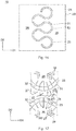
- Fig. 4 is an enlarged plan view of the control region 23 and the non-control region 26 of the wiring board 10.
- the wiring 52 is disposed at a location adjacent to the first surface 21 of the substrate 20, and then the tensile stress is removed from the substrate 20.
- tensile stress is applied to the substrate 20 in the first direction D1 and the second direction D2.
- the substrate 20 contracts in the first direction D1 and the second direction D2.
- wrinkles resulting from the contraction of the substrate 20 in the first direction D1 and wrinkles resulting from the contraction of the substrate 20 in the second direction D2 both appear in the non-control region 26.
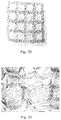
- a plurality of ridges 27 appear in the non-control region 26, the ridges 27 extending in different directions and crossing each other.
- Each ridge 27 tends to have a greater amplitude and a smaller radius of curvature in a portion of the ridge 27 that intersects another ridge 27 than in other portions of the ridge 27.
- the ridges 27 that extend in different directions and cross each other are referred to also as intersecting ridge group 28.
- the non-control region 26 may include a plurality of intersecting ridge groups 28.
- the control region 23 has an anisotropy such that the control region 23 extends in the first direction D1 as described above. Further, the control region 23 is sandwiched by adjacent portions of the non-control region 26 in the second direction D2, which is transverse to the direction in which the control region 23 extends. Thus, wrinkles resulting from the contraction of the substrate 20 in the second direction D2, which is transverse to the direction in which the control region 23 extends, are unlikely to appear in the control region 23. This means that wrinkles resulting from the contraction of the substrate 20 in the first direction D1 appear in the control region 23. For example, as illustrated in Fig.
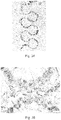
- a plurality of ridges 32 appear in the control region 23, the ridges 32 extending in a direction transverse to the first direction D1 and being arranged in the first direction D1.
- the ridges 32 may extend across the control region 23 in the direction transverse to the first direction D1 in which the wiring 52 extends.
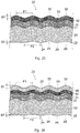
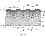
- Fig. 5 is a cross-sectional view, taken along a line C-C, of the control region 23 illustrated in Fig. 4 .
- the ridges 32 are raised portions of a surface of the wiring board 10 that is located at the first surface 21 side of the substrate 20, the raised portions being raised in a direction normal to the first surface 21.
- the ridges 32 are arranged in the first direction D1 in which the wiring 52 extends.
- a valley 33 is present between each two ridges 32 that are adjacent to each other in the direction in which the wiring 52 extends.
- an area where the ridges 32 and the valleys 33 are arranged repeatedly in a specific direction is referred to also as bellows-shaped part.
- reference sign S1 denotes the amplitude, in a direction normal to the first surface 21 of the substrate 20, of the ridges 32 arranged in the direction in which the wiring 52 extends.
- the amplitude S1 is, for example, greater than or equal to 1 ⁇ m, and more preferably greater than or equal to 10 ⁇ m. Making the amplitude S1 greater than or equal to 10 ⁇ m allows the wiring 52 to readily deform following stretching of the substrate 20.
- the amplitude S1 may be, for example, less than or equal to 500 ⁇ m.
- the amplitude S1 is calculated as follows, for example.
- the distance, in the direction normal to the first surface 21, between each ridge 32 and the corresponding valley 33 that are adjacent to each other is measured over a certain range of area in the direction in which the wiring 52 extends, and the mean of such distances is found as the amplitude S1.
- the "certain range of area in the longitudinal direction of the wiring 52" is, for example, 10 mm.
- a measuring instrument used to measure distance may be a non-contact type measuring instrument employing a laser microscope or other devices, or may be a contact type measuring instrument. Alternatively, distance may be measured based on an image such as a cross-section photograph. The same applies to the method for calculating an amplitude S3 described later.
- reference sign F1 denotes the cycle of the ridges 32 arranged in the direction in which the wiring 52 extends.
- the cycle F1 of the ridges 32 is calculated by measuring, over a certain range of area in the direction in which the wiring 52 extends, the interval between individual ridges 32 in the direction in which the wiring 52 extends, and finding the mean of such intervals.
- the cycle F1 is, for example, greater than or equal to 10 ⁇ m, and more preferably greater than or equal to 100 ⁇ m. Making the cycle F1 greater than or equal to 10 ⁇ m helps to ensure that the ridges 32 extending in different directions do not cross each other.
- the cycle F1 is, for example, less than or equal to 100 mm, and more preferably less than or equal to 10 mm.
- the control region 23 deforms such that the ridges 32 arranged in the first direction D1 appear in the control region 23.
- the dimension U11 of the control region 23 in the first direction D1 is sufficiently large relative to the cycle F1 of the ridges 32.
- the dimension U11 of the control region 23 in the first direction D1 may be, for example, greater than or equal to 2 times, greater than or equal to 5 times, greater than or equal to 7 times, greater than or equal to 10 times, or greater than or equal to 15 times the cycle F1 of the ridges 32.
- the dimension U21 of the control region 23 in the second direction D2 may be, for example, less than or equal to 20 times, less than or equal to 10 times, less than or equal to 7 times, less than or equal to 5 times, or less than or equal to 3 times the cycle F1 of the ridges 32.
- a plurality of ridges 24 and a plurality of valleys 25, which are arranged in the direction in which the wiring 52 extends, may appear also on a surface of the wiring board 10 located at the second surface 22 side of the substrate 20.
- each ridge 24 located at the second surface 22 side appears at a location overlapping the corresponding valley 33 located at the first surface 21 side
- each valley 25 located at the second surface 22 side appears at a location overlapping the corresponding ridge 32 located at the first surface 21 side.
- reference sign S3 denotes the amplitude, in the direction normal to the second surface 22 of the substrate 20, of the ridge 24 that appears on a surface of the wiring board 10 located at the second surface 22 side of the substrate 20 and are arranged in the direction in which the wiring 52 extends.
- the amplitude S3 of the ridge 24 located at the second surface 22 side may or may not be the same as the amplitude S1 of the ridge 32 located at the first surface 21 side.
- the amplitude S3 of the ridge 24 located at the second surface 22 side may be less than the amplitude S1 of the ridge 32 located at the first surface 21 side.
- the amplitude S3 of the ridge 24 located at the second surface 22 side may be less than or equal to 0.9 times, less than or equal to 0.8 times, or less than or equal to 0.6 times the amplitude S1 of the ridge 32 located at the first surface 21 side. Further, the amplitude S3 of the ridge 24 located at the second surface 22 side may be greater than or equal to 0.1 times, or greater than or equal to 0.2 times the amplitude S1 of the ridge 32 located at the first surface 21 side.
- the amplitude S3 of the ridge 24 located at the second surface 22 side is less than the amplitude S1 of the ridge 32 located at the first surface 21 side
- reference sign F3 denotes the cycle of the ridges 24 that appear on a surface of the wiring board 10 located at the second surface 22 side of the substrate 20 and are arranged in the direction in which the wiring 52 extends.
- the cycle F3 of the ridges 24 located at the second surface 22 side may be the same as the cycle F1 of the ridges 32 located at the first surface 21 side.
- reference signs M1 and M2 respectively denote the width of the ridge 32 and the width of the valley 33 in the direction in which the wiring 52 extends when the wiring board 10 is in its non-tensioned state.
- the width M1 of the ridge 32 and the width M2 of the valley 33 are substantially equal.
- the ratio of the ridges 32 in the bellows-shaped part with the wiring board 10 in its non-tensioned state is represented by reference sign X1.
- the ratio X1 is calculated as M1/(M1 + M2).
- the ratio X1 is, for example, greater than or equal to 0.40 and less than or equal to 0.60.
- Fig. 6 is another exemplary cross-sectional view, taken along the line C-C, of the control region 23 illustrated in Fig. 4 .
- the cycle F3 of the ridges 24 located at the second surface 22 side may be greater than the cycle F1 of the ridges 32 located at the first surface 21 side.
- the cycle F3 of the ridges 24 located at the second surface 22 side may be greater than or equal to 1.1 times, greater than or equal to 1.2 times, greater than or equal to 1.5 times, or greater than or equal to 2.0 times the cycle F1 of the ridges 32 located at the first surface 21 side.
- the cycle F3 of the ridges 24 located at the second surface 22 side is greater than the cycle F1 of the ridges 32 located at the first surface 21 side
- Fig. 7 is another exemplary cross-sectional view, taken along the line C-C, of the control region 23 illustrated in Fig. 4 .
- the ridges 24 and the valleys 25 located at the second surface 22 side may be shifted in position by an amount J from where the corresponding valleys 33 and the corresponding ridges 32 located at the first surface 21 side.
- the amount of shift J may be, for example, greater than or equal to 0.1 ⁇ F1, or greater than or equal to 0.2 ⁇ F1.
- Fig. 8A is another exemplary cross-sectional view, taken along the line C-C, of the control region 23 illustrated in Fig. 4 .
- the area between each two ridges 32 that are adjacent to each other in the direction in which the wiring 52 extends may define a flat surface.
- the amplitude S1 is calculated as follows, for example. The distance, in the direction normal to the first surface 21, between the flat surface and each of adjacent ridges 32 is measured over a certain range of area in the direction in which the wiring 52 extends, and the mean of such distances is found as the amplitude S1.
- reference sign M1 denotes the width of the ridge 32 in the direction in which the wiring 52 extends.
- the width M1 is, for example, greater than or equal to 1 ⁇ m, and more preferably greater than or equal to 10 ⁇ m. Making the width M1 greater than or equal to 1 ⁇ m helps to prevent or inhibit a decrease in the radius of curvature of the ridge 32.
- the width M1 of the ridge 32 in the direction in which the wiring 52 extends may be less than the width M2 of the valley 33.
- the width M1 of the ridge 32 may be greater than or equal to 0.3 times, greater than or equal to 0.4 times, greater than or equal to 0.5 times, or greater than or equal to 0.6 times the width M2 of the valley 33. Further, the width M1 of the ridge 32 may be less than or equal to 0.9 times, less than or equal to 0.8 times, or less than or equal to 0.7 times the width M2 of the valley 33.
- the ridge 32 and the valley 33 are discriminated from each other with the midpoint of the amplitude S1 of the bellows-shaped part defined as their boundary.
- the width M2 of the valley 33 in the direction in which the wiring 52 extends may be less than the width M1 of the ridge 32.
- the width M2 of the valley 33 may be greater than or equal to 0.05 times, greater than or equal to 0.1 times, greater than or equal to 0.2 times, or greater than or equal to 0.3 times the width M1 of the ridge 32.
- the width M2 of the valley 33 may be less than or equal to 0.9 times, less than or equal to 0.8 times, or less than or equal to 0.7 times the width M1 of the ridge 32.
- the width M1 of the ridge 32 appearing in the control region 23 is greater than the width W2 of the ridge 27 appearing in the non-control region 26.
- the width M1 of the ridge 32 in the control region 23 may be greater than or equal to 1.1 times, greater than or equal to 1.2 times, greater than or equal to 1.5 times, or greater than or equal to 2.0 times the width W2 of the ridge 27 in the non-control region 26.
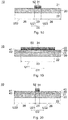
- a method for manufacturing the wiring board 10 is described below with reference to Fig. 9A to Fig. 9D .
- a substrate preparation step is performed.
- the substrate 20 having stretchability is prepared.
- an elongation step is performed.
- the substrate 20 is elongated by applying a tensile stress T to the substrate 20 in the first direction D1 and in the second direction D2 transverse to the first direction D1.
- the substrate 20 has a stretch percentage of, for example, greater than or equal to 10% and less than or equal to 200% in the first direction D1 and the second direction D2.
- the stretching step may be performed with the substrate 20 heated, or may be performed with the substrate 20 at room temperature. If the substrate 20 is to be heated, the substrate 20 is heated to a temperature of, for example, greater than or equal to 50°C and less than or equal to 100°C.
- a wiring step is performed.
- the wiring 52 is disposed on the first surface 21 of the substrate 20 that is being elongated due to the tensile stress T.
- a conductive paste containing a base material and conductive particles is printed onto the first surface 21 of the substrate 20.
- the reinforcing part 31 is disposed at the first surface 21 side of the substrate 20 that is being elongated due to the tensile stress T.
- a material including resin that constitutes the reinforcing part 31 is printed onto the wiring 52 by screen printing or other methods.
- a contraction step is performed.
- the tensile stress T is removed from the substrate 20.
- the substrate 20 contracts in the first direction D1 in which the wiring 52 extends.
- the substrate 20 also contracts in the second direction D2 transverse to the first direction D1.
- the substrate 20 has the control region 23, which overlaps the reinforcing part 31 overlapping the wiring 52, and the non-control region 26, which does not overlap the reinforcing part 31 and is positioned to sandwich the control region 23 in the second direction D2 orthogonal to the first direction D1 in which the wiring 52 extends.
- the wiring 52 and the reinforcing part 31 deform following the contraction of the substrate 20, which gives rise to the appearance of the ridges 32 arranged in the first direction D1.
- the wiring 52 and the reinforcing part 31 are able to follow the stretching of the substrate 20 by deforming in a manner that reduces the amplitude of the ridges 32, in other words, in a manner that eliminates the ridges 32.
- This helps to prevent or inhibit the wiring 52 from increasing in overall length or decreasing in cross-sectional area as the substrate 20 is stretched. This in turn helps to prevent or inhibit the resistance of the wiring 52 from increasing due to the stretching of the wiring board 10. It is also possible to prevent or inhibit the wiring 52 from sustaining damage such as cracking.
- the presence of the reinforcing part 31 helps to prevent or inhibit the wiring 52 from deforming as the substrate 20 contracts.
- This helps to prevent or inhibit formation, in the control region 23, of other ridges extending in a direction different from the ridges 32 arranged in the first direction D1.
- This helps to prevent or inhibit wrinkles extending in different directions from interfering with each other in the control region 23.
- a local increase in the amplitude of the ridges 32 appearing in the control region 23, or a local disturbance in the cycle of the ridges 32 can be prevented or inhibited.
- the standard deviation of the cycles of the ridges 32 can be made less than or equal to three-quarters, and more preferably less than or equal to one-half of the mean cycle.
- the ridges 32 form as a result of contraction of the substrate 20, and thus it is not easy to make the standard deviation of the cycles of the ridges 32 zero.
- the standard deviation of the cycles of the ridges 32 may be, for example, greater than or equal to 1/50, greater than or equal to 1/10, or greater than or equal to 1/4 of the mean cycle. Further, a decrease in the radius of curvature of the ridges 32 appearing in the control region 23 can be prevented or reduced.
- the substrate 20 undergoes contraction in the non-control region 26 positioned to sandwich the control region 23 in the second direction D2.
- the substrate 20 stretches in the non-control region 26, which also allows the wiring board 10 to elongate.
- the embodiment allows the wiring board 10 to elongate in the first direction D1 and the second direction D2 during its use while preventing or inhibiting the wiring 52 located in the control region 23 from sustaining damage such as fracturing.
- the wiring board 10 can be thus used for applications that require the wiring board 10 to be stretchable in various directions.
- the value of resistance that the wiring 52 has in a first state which is a state with no tensile stress applied to the substrate 20 in the first direction D1 is herein referred to as first resistance.
- the value of resistance that the wiring 52 has in a second state which is a state with the substrate 20 elongated by 30% relative to the first state by application of tensile stress to the substrate 20 in the first direction D1, is referred to as second resistance.
- the ratio of the absolute difference between the first resistance and the second resistance to the first resistance can be made less than or equal to 20%, more preferably less than or equal to 10%, and still more preferably less than or equal to 5%.
- Fig. 36 is an enlarged cross-sectional view of the wiring board 10 with the wiring board 10 elongated by 25% relative to the first state by application of tension to the wiring board 10 in the first direction D1.
- reference sign S10 denotes the amplitude of the bellows-shaped part with the wiring board 10 elongated by 25%.
- Reference sign F1 denotes the cycle of the bellows-shaped part with the wiring board 10 elongated by 25%.
- the amplitude S10 of the bellow-shaped part of the wiring board 10 that is being elongated by 25% may be, for example, less than or equal to 0.8 times, less than or equal to 0.7 times, or less than or equal to 0.6 times the amplitude S1 of the bellows-shaped part of the wiring board 10 in its non-elongated state.
- the amplitude S10 may be, for example, greater than or equal to 0.2 times, greater than or equal to 0.3 times, or greater than or equal to 0.4 times the amplitude S1.
- reference signs M11 and M21 denote the respective widths, in the direction in which the wiring 52 extends, of the ridge 32 and valley 33 of the bellows-shaped part of the wiring board 10 that is being elongated by 25%.
- the width M11 of the ridge 32 and the width M21 of the valley 33 of the wiring board 10 that is being elongated by 25% are greater than the width M1 of the ridge 32 and the width M2 of the valley 33 of the wiring board 10 in its non-elongated state.
- the respective widths of the ridge 32 and valley 33 of the bellows-shaped part may be increased while maintaining their relative ratios.
- the ratio of the ridges 32 in the bellows-shaped part with the wiring board 10 in its non-tensioned state is represented by reference sign X2.
- the ratio X2 is calculated as M11/(M11 + M21).
- the ratio X2 is substantially equal to the above-mentioned ratio X1 for the wiring board 10 in its non-tensioned state, and is, for example, greater than or equal to 0.40 and less than or equal to 0.60.
- the absolute difference between the ratio X1 and the ratio X2 may be, for example, less than or equal to 0.20, less than or equal to 0.15, less than or equal to 0.10, less than or equal to 0.08, less than or equal to 0.06, or less than or equal to 0.04.
- the wiring 52 is made of copper, has a thickness of 1 ⁇ m, and has a width of 200 ⁇ m.
- the percent elongation of the substrate 20 in the wiring step described later is 60%.
- the percent elongation of the substrate 20 is 25% at the time when the amplitude of the bellows-shaped part as well as the respective widths of the ridge 32 and the valley 33 are measured with the wiring board 10 in its tensioned state.
- Exemplary fields of application of the wiring board 10 may include healthcare, medical care, nursing, electronics, sports/fitness, beauty care, mobility, stock breeding/pets, amusement, fashion/apparel, security, military, distribution, education, building materials/furniture/decoration, environmental energy, forestry and fisheries, and robotics.
- products designed for attachment to a part of a human body such as an arm are fabricated by using the wiring board 10 according to the present embodiment.
- the stretchability of the wiring board 10 helps to ensure, for example, tight contact of the wiring board 10 with a part of a human body when attached to the human body in its elongated state. This helps to provide superior wearing comfort.
- the wiring board 10 is capable of elongation, which allows the wiring board 10 to be installed or incorporated in a manner that conforms not only to the body of a living creature such as a human being but also to a curved surface or a three-dimensional shape.
- Examples of the above-mentioned products may include vitals sensors, masks, hearing aids, toothbrushes, adhesive plasters, poultices, contact lenses, prosthetic arms, prosthetic legs, artificial eyes, catheters, gauze, medicine packs, bandages, disposable bioelectrodes, diapers, rehabilitation equipment, consumer electronics, displays, signage, personal computers, mobile phones, mouses, speakers, sportswear, wristbands, headbands, gloves, swimsuits, athletic supporters, balls, sports gloves, rackets, clubs, bats, fishing rods, relay batons/gymnastics items or grips thereof, physical training equipment, swim rings, tents, swimsuits, number clothes, goal nets, goal tapes, impregnated beauty masks, electrostimulation slimming products, heating packs, artificial nails, tattoos, seats for vehicles such as automobiles, airplanes, trains, ships, bicycles, baby strollers, drones, or wheelchairs, instrument panels, tires, interior materials, exterior materials, saddles, handles, roads, rails, bridges
- Fig. 10 is a plan view of the wiring board 10 according to a first modification.
- the reinforcing part 31 defining the control region 23 may extend so as to overlap a plurality of pieces of the wiring 52 extending in the first direction D1 and arranged in the second direction D2.
- the configuration of the wiring board 10 illustrated in Fig. 10 also helps to prevent or inhibit appearance, in the control region 23, of the ridges 32 extending in different directions and crossing each other.
- Fig. 11 is a plan view of the wiring board 10 according to a second modification.
- the wiring 52 includes first wiring 521 extending in the first direction D1, and second wiring 522 extending in the second direction D2 transverse to the first direction D1.
- the first wiring 521 and the second wiring 522 may intersect each other.
- the first wiring 521 and the second wiring 522 may be arranged such that the wiring 52 defines a grid-like pattern.
- the reinforcing part 31 likewise includes a portion extending in the first direction D1, and a portion extending in the second direction D2.
- the control region 23 defined by the reinforcing part 31 likewise includes a first control region 231 extending in the first direction D1, and a second control region 232 extending in the second direction D2 transverse to the first direction D1.
- an area bounded by the first control region 231 and the second control region 232 defines the non-control region 26.
- the non-control region 26 is positioned to sandwich the second control region 232 in the first direction D1. Further, the non-control region 26 is positioned to sandwich the first control region 231 in the second direction D2.
- Fig. 12 is an enlarged plan view of the control region 23 and the non-control region 26 of the wiring board 10 illustrated in Fig. 11 .
- the wiring 52 is disposed on the first surface 21 of the substrate 20, and then the tensile stress is removed from the substrate 20.
- tensile stress is applied to the substrate 20 in the first direction D1 and the second direction D2, and then the tensile stress is removed from the substrate 20.
- the ridges 27 extending in different directions and crossing each other appear in the non-control region 26 as illustrated in Fig. 12 .
- the control region 23 includes the first control region 231, which has an anisotropy such that the first control region 231 extends in the first direction D1, and the second control region 232, which has an anisotropy such that the second control region 232 extends in the second direction D2.
- the first control region 231 is sandwiched by adjacent portions of the non-control region 26 in the second direction D2.
- wrinkles resulting from the contraction of the substrate 20 in the second direction D2 are unlikely to appear in the first control region 231.
- the ridges 32 extending in a direction transverse to the first direction D1 and arranged in the first direction D1 appear in the first control region 231.
- the ridge 32 may extend across the first control region 231 in the direction transverse to the first direction D1.
- the second control region 232 is sandwiched by adjacent portions of the non-control region 26 in the first direction D1.
- wrinkles resulting from the contraction of the substrate 20 in the first direction D1 are unlikely to appear in the second control region 232.
- the ridges 32 extending in a direction transverse to the second direction D2 and arranged in the second direction D2 appear in the second control region 232.
- the ridge 32 may extend across the first control region 231 in the direction transverse to the second direction D2.
- the ridge 32 may also appear in a portion of the control region 23 where the first control region 231 and the second control region 232 cross each other.
- the ridge 32 may extend in any direction.
- the ridge 32 may extend in a direction different from both the first direction D1 and the second direction D2.
- the second modification by controlling the direction in which wrinkles appearing in the control region 23 including the first and second control regions 231 and 232 extend, it is possible to prevent or inhibit appearance, in the control region 23, of the ridges 32 that extend in different directions and cross each other. This helps to prevent or inhibit the ridges 32 appearing in the control region 23 from locally increasing in amplitude. This also helps to prevent or inhibit the ridges 32 appearing in the control region 23 from decreasing in radius of curvature. This helps to prevent or inhibit the wiring 52 located in the control region 23 from sustaining damage such as fracturing.
- Fig. 13 is a plan view of the wiring board 10 according to a third modification.
- the wiring 52 includes the first wiring 521 extending in the first direction D1, the second wiring 522 extending in the second direction D2 transverse to the first direction D1, and third wiring 523 located between the first wiring 521 and the second wiring 522 and extending in a third direction D3 transverse to the first direction D1 and to the second direction D2.
- the reinforcing part 31 likewise includes a portion extending in the first direction D1, a portion extending in the second direction D2, and a portion extending in the third direction D3.
- control region 23 defined by the reinforcing part 31 also includes the first control region 231 extending in the first direction D1, the second control region 232 extending in the second direction D2 transverse to the first direction D1, and a third control region 233 located between the first control region 231 and the second control region 232 and extending in the third direction D3 transverse to the first direction D1 and to the second direction D2.
- the non-control region 26 is positioned to sandwich the first control region 231 in the second direction D2 orthogonal to the first direction D1.
- the non-control region 26 is positioned to sandwich the second control region 232 in the first direction D1 orthogonal to the second direction D2.
- the non-control region 26 is positioned to sandwich the third control region 233 in a direction orthogonal to the third direction D3.
- Fig. 14 is an enlarged plan view of the control region 23 and the non-control region 26 of the wiring board 10 illustrated in Fig. 13 .
- the wiring 52 is disposed on the first surface 21 of the substrate 20, and then the tensile stress is removed from the substrate 20.
- tensile stress is applied to the substrate 20 in the first direction D1 and the second direction D2, and then the tensile stress is removed from the substrate 20.
- the ridges 27 extending in different directions and crossing each other appear in the non-control region 26 as illustrated in Fig. 14 .
- the control region 23 includes the first control region 231, which has an anisotropy such that the first control region 231 extends in the first direction D1, the second control region 232, which has an anisotropy such that the second control region 232 extends in the second direction D2, and the third control region 233, which has an anisotropy such that the third control region 233 extends in the third direction D3.
- the ridges 32 extending in a direction transverse to the first direction D1 and arranged in the first direction D1 appear, and in the second control region 232, the ridges 32 extending in a direction transverse to the second direction D2 and arranged in the second direction D2 appear.
- the substrate 20 contracts in the third direction D3, which is transverse to the first direction D1 and the second direction D2, and in a direction orthogonal to the third direction D3.
- the third control region 233 is sandwiched by adjacent portions of the non-control region 26 in the direction orthogonal to the third direction D3.
- the ridges 32 extending in a direction transverse to the third direction D3 and arranged in the third direction D3 appear in the third control region 233.
- the ridge 32 may extend across the third control region 233 in the direction transverse to the third direction D3.
- the third modification by controlling the direction in which wrinkles appearing in the control region 23 including the first, second, and third control regions 231, 232, and 233 extends, it is possible to prevent or inhibit appearance, in the control region 23, of the ridges 32 that extend in different directions and cross each other. This helps to prevent or inhibit the ridges 32 appearing in the control region 23 from locally increasing in amplitude. This also helps to prevent or inhibit the ridges 32 appearing in the control region 23 from decreasing in radius of curvature. This helps to prevent or inhibit the wiring 52 located in the control region 23 from sustaining damage such as fracturing.
- Fig. 15 is a plan view of the wiring board 10 according to a fourth modification.
- a plurality of control regions 23 may be arranged in a direction transverse to the direction in which the control regions 23 extend, the control regions 23 each including portions extending in a plurality of directions, such as the first control region 231, the second control region 232, and the third control region 233.
- the region between two adjacent control regions 23 may define the non-control region 26.
- each control region 23 can be sandwiched by adjacent portions of the non-control region 26 in a direction orthogonal to the direction in which the control region 23 extends, that is, in a direction orthogonal to the direction in which the wiring 52 extends.
- Fig. 16 is a plan view of the wiring board 10 according to a fifth modification.
- the wiring 52, and the reinforcing part 31 overlapping the wiring 52 may each have a curved portion that is curved in plan view.
- the wiring 52 and the reinforcing part 31 have a so-called horseshoe shape.
- elongating the wiring board 10 allows the wiring 52 and the reinforcing part 31 to deform such that their curved portion increases in radius of curvature. This helps to prevent or inhibit the wiring 52 from sustaining damage such as fracturing due to the stretching of the wiring board 10.
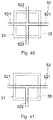
- Fig. 17 is an enlarged plan view of the control region 23 and the non-control region 26 of the wiring board 10 illustrated in Fig. 16 .
- the control region 23 defined by the reinforcing part 31 is sandwiched by adjacent portions of the non-control region 26 in a direction orthogonal to the direction in which the control region 23 extends.
- the wiring 52 is disposed on the first surface 21 of the substrate 20, and then the tensile stress is removed from the substrate 20.
- tensile stress is applied to the substrate 20 in the first direction D1 and the second direction D2, and then the tensile stress is removed from the substrate 20.
- the ridges 27 extending in different directions and crossing each other appear in the non-control region 26 as illustrated in Fig. 17 .
- the control region 23 is sandwiched by adjacent portions of the non-control region 26 in a direction orthogonal to the direction in which the control region 23 extends.
- wrinkles resulting from the contraction of the substrate 20 in the direction orthogonal to the direction in which the control region 23 extends are unlikely to appear in the control region 23.
- wrinkles resulting from the contraction of the substrate 20 in the direction in which the control region 23 extends appear in the control region 23.
- the ridges 32 extending in a direction transverse to the direction in which the control region 23 extends and arranged in the direction in which the control region 23 extends appear in the control region 23.
- the ridge 32 may extend across the control region 23 in the direction transverse to the direction in which the control region 23 extends.
- the fifth modification by controlling the direction in which wrinkles generated in the control region 23 extend, it is possible to prevent or inhibit appearance, in the control region 23, of the ridges 32 that extend in different directions and cross each other. This helps to prevent or inhibit the ridges 32 appearing in the control region 23 from locally increasing in amplitude. This also helps to prevent or inhibit the ridges 32 appearing in the control region 23 from decreasing in radius of curvature. This helps to prevent or inhibit the wiring 52 located in the control region 23 from sustaining damage such as fracturing.
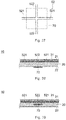
- Fig. 18 is a cross-sectional view of the wiring board 10 according to a sixth modification. As with Fig. 3 mentioned above, Fig. 18 illustrates a cross-section of the wiring board 10 taken in a direction orthogonal to the direction in which the wiring 52 extends.
- the reinforcing part 31 and the control region 23 may each have a larger dimension than the wiring 52 in the direction orthogonal to the direction in which the wiring 52 extends.
- the wiring 52 may be covered on its surface and sides by the reinforcing part 31.
- a seventh modification is directed to a case in which the wiring 52 is supported by a support substrate.
- Figs. 19 and 20 are cross-sectional views of the wiring board 10 according to the seventh modification.
- Fig. 19 illustrates a cross-section of the wiring board 10 taken in a direction in which the wiring 52 extends.
- Fig. 20 illustrates a cross-section of the wiring board 10 taken in a direction orthogonal to the direction in which the wiring 52 extends.
- the wiring board 10 includes at least the substrate 20, the support substrate 40, the wiring 52, and the reinforcing part 31.
- the support substrate 40 is a part with a lower stretchability than the substrate 20.
- the support substrate 40 includes a second surface 42 located toward the substrate 20, and a first surface 41 located opposite to the second surface 42. In the example illustrated in Figs. 19 and 20 , the support substrate 40 supports the wiring 52 at the first surface 41 side of the support substrate 40.
- the support substrate 40 is joined to the first surface of the substrate 20 at the second surface 42 side.
- an adhesive layer 60 containing an adhesive may be disposed between the substrate 20 and the support substrate 40.
- the adhesive layer 60 may be made of, for example, an acrylic-based adhesive or a silicone-based adhesive.
- the adhesive layer 60 has a thickness of, for example, greater than or equal to 5 ⁇ m and less than or equal to 200 ⁇ m.
- the second surface 42 of the support substrate 40 may be joined to the first surface 21 of the substrate 20 by a method that involves subjecting a non-adhesive surface to molecular modification to achieve molecular adhesive bonding. In this case, no adhesive layer may be disposed between the substrate 20 and the support substrate 40.
- the reinforcing part 31 is stacked over the wiring 52 at the first surface 41 side of the support substrate 40.
- the reinforcing part 31 may be in contact with the wiring 52, or another layer such as an insulating layer may be interposed between the wiring 52 and the reinforcing part 31.
- the reinforcing part 31 may be located at the second surface 42 side of the support substrate 40.
- Fig. 21 is an enlarged plan view of the control region 23 of the wiring board 10 illustrated in Fig. 19 .
- the ridges 32 form on the support substrate 40, the wiring 52, and the reinforcing part 31 as illustrated in Fig. 21 .
- the characteristics and dimensions of the support substrate 40 are designed to facilitate such formation of the ridges 32.
- the support substrate 40 has an elastic modulus greater than the first elastic modulus of the substrate 20.
- the elastic modulus of the support substrate 40 is sometimes referred to also as third elastic modulus.
- the support substrate 40 may support the wiring 52 at the second surface 42 side.
- the reinforcing part 31 may be disposed at the first surface 41 side of the support substrate 40, or may be disposed at the second surface 42 side of the support substrate 40.
- the third elastic modulus of the support substrate 40 is, for example, greater than or equal to 100 MPa, and more preferably greater than or equal to 1 GPa. Further, the third elastic modulus of the support substrate 40 may be greater than or equal to 100 times and less than or equal to 50000 times, and preferably greater than or equal to 1000 times and less than or equal to 10000 times the first elastic modulus of the substrate 20. Setting the third elastic modulus of the support substrate 40 as mentioned above helps to ensure that the cycle F1 of the ridges 32 does not become too small. This also helps to prevent or inhibit local bending in the ridges 32.
- An excessively low elastic modulus of the support substrate 40 causes the support substrate 40 to deform easily during formation of the reinforcing part 31, which makes it difficult to align the reinforcing part 31 with respect to the wiring 52.
- An excessively high elastic modulus of the support substrate 40 makes it difficult for the substrate 20 to restore its original shape when relaxed, and makes the substrate 20 susceptible to cracking or fracturing.
- the support substrate 40 has a thickness of, for example, greater than or equal to 500 nm and less than or equal to 10 ⁇ m, and more preferably greater than or equal to 1 ⁇ m and less than or equal to 5 ⁇ m.
- An excessively small thickness of the support substrate 40 makes handling of the support substrate 40 difficult during manufacture of the support substrate 40 or during formation of a part over the support substrate 40.
- An excessively large thickness of the support substrate 40 makes it difficult for the substrate 20 to restore its original shape when relaxed, which may make it difficult to achieve desired stretching and contraction of the substrate 20.
- Exemplary suitable materials for the support substrate 40 may include polyethylene naphthalate, polyimide, polyethylene terephthalate, polycarbonate, and acrylic resin. Among these, polyethylene naphthalate or polyimide, which exhibits superior durability and thermal resistance, may be preferably used.
- the third elastic modulus of the support substrate 40 may be less than or equal to 100 times the first elastic modulus of the substrate 20.
- the third elastic modulus of the support substrate 40 may be calculated by the same method as that used for calculating the elastic modulus of the substrate 20 or the reinforcing part 31.
- the support substrate 40 is prepared.
- the wiring 52 is disposed on the first surface 41 of the support substrate 40.
- a metal layer such as a copper layer is formed by vapor deposition or other methods on the first surface 41 of the support substrate 40.
- the metal layer is processed by photolithography and etching.
- the wiring 52 on the first surface 41 is thus obtained.
- the reinforcing part 31 is disposed at the first surface 41 side of the support substrate 40.
- a material containing resin that constitutes the reinforcing part 31 is printed onto the wiring 52 by screen printing or other methods.
- the support substrate 40 with the wiring 52 and the reinforcing part 31 disposed over the first surface 41 is thus obtained as illustrated in Fig. 22A .
- an elongation step is performed.
- the substrate 20 is elongated by applying a tensile stress T to the substrate 20 in the first direction D1 and in the second direction D2 transverse to the first direction D1.
- a wiring step is performed.
- the wiring step the wiring 52 is disposed at a location adjacent to the first surface 21 of the substrate 20 that is being elongated due to the tensile stress T.
- the wiring step according to the seventh modification with the wiring 52 and the reinforcing part 31 disposed over the support substrate 40 as described above, the second surface 42 of the support substrate 40 is joined to the first surface 21 of the substrate 20 as illustrated in Fig. 22C .
- the adhesive layer 60 may be disposed between the substrate 20 and the support substrate 40.
- a contraction step is performed.
- the tensile stress T is removed from the substrate 20.
- the substrate 20 contracts in the first direction D1 in which the wiring 52 extends.
- the substrate 20 also contracts in the second direction D2 transverse to the first direction D1.
- the substrate 20 has the control region 23, which overlaps the reinforcing part 31 overlapping the wiring 52, and the non-control region 26, which does not overlap the reinforcing part 31 and is positioned to sandwich the control region 23 in the second direction D2 orthogonal to the first direction D1 in which the wiring 52 extends.
- the control region 23 includes the ridges 32 arranged in the direction in which the wiring 52 extends.
- the support substrate 40, the wiring 52, and the reinforcing part 31 are able to follow the stretching of the substrate 20 by deforming in a manner that reduces the amplitude of the ridges 32, in other words, in a manner that eliminates the ridges 32.
- This helps to prevent or inhibit the wiring 52 from increasing in overall length or decreasing in cross-sectional area as the substrate 20 is stretched. This in turn helps to prevent or inhibit the resistance of the wiring 52 from increasing due to the stretching of the wiring board 10. It is also possible to prevent or inhibit the wiring 52 from sustaining damage such as cracking.
- the presence of the reinforcing part 31 helps to prevent or inhibit the support substrate 40 and the wiring 52 from deforming following the contraction of the substrate 20.
- This makes it possible to prevent or inhibit appearance, in the control region 23, of the ridges 32 extending in different directions and crossing each other. This helps to prevent or inhibit the ridges 32 appearing in the control region 23 from locally increasing in amplitude. This also helps to prevent or inhibit the ridges 32 appearing in the control region 23 from decreasing in radius of curvature. This helps to prevent or inhibit the wiring 52 located in the control region 23 from sustaining damage such as fracturing.
- Fig. 23 is a cross-sectional view of the wiring board 10 according to an eighth modification.
- Fig. 23 illustrates a cross-section of the wiring board 10 including the support substrate 40, taken in a direction orthogonal to the direction in which the wiring 52 extends.
- the reinforcing part 31 and the control region 23 may each have a larger dimension than the wiring 52 in a direction orthogonal to the direction in which the wiring 52 extends.
- the wiring 52 may be covered on its surface and sides by the reinforcing part 31.
- Fig. 24 is a cross-sectional view of the wiring board 10 according to a ninth modification.
- Fig. 24 illustrates a cross-section of the wiring board 10 taken in a direction in which the wiring 52 extends.
- the wiring board 10 may include an electronic component 51 electrically connected to the wiring 52.
- the electronic component 51 is located at the first surface 41 side of the support substrate 40.
- the wiring board 10 may be designed to allow mounting of the electronic component 51 that is electrically connected to the wiring 52.
- the electronic component 51 may have an electrode that is connected to the wiring 52.
- the wiring board 10 has a connection part that is in contact with the electrode of the electronic component 51 and electrically connected to the wiring 52.
- the connection part is, for example, a pad.
- the electronic component 51 may not have an electrode that is connected to the wiring 52.
- the electronic component 51 may include a part integral with at least one of a plurality of elements constituting the wiring board 10.
- Examples of such an electronic component 51 may include an electronic component including a conductive layer integral with the conductive layer constituting the wiring 52 of the wiring board 10, and an electronic component including a conductive layer located at a position different from the conductive layer constituting the wiring 52.
- the electronic component 51 may be a pad formed by a conductive layer that has a greater width than the conductive layer constituting the wiring 52 in plan view. For example, an inspection probe, or a terminal for software rewrites is connected to the pad.
- the electronic component 51 may be a wiring pattern including a conductive layer extending in helical form in plan view. As described above, a part with a conductive layer patterned and imparted with a predetermined function may also serve as the electronic component 51.
- the electronic component 51 may be an active component, may be a passive component, or may be an electromechanical component.
- Examples of the electronic component 51 may include transistors, large scale integration (LSI), micro electro mechanical systems (MEMS), relays, light-emitting devices such as LEDs, OLEDs, and LCDs, sensors, sound-emitting components such as buzzers, vibrating components that generate vibration, cooling/heat-generating components such as Peltier devices or heating wires that control cooling/heat generation, resistors, capacitors, inductors, piezoelectric elements, switches, and connectors.
- sensors are preferably used.
- sensors may include temperature sensors, pressure sensors, light sensors, photoelectric sensors, proximity sensors, shearing force sensors, biometric sensors, laser sensors, microwave sensors, humidity sensors, distortion sensors, gyro sensors, acceleration sensors, displacement sensors, magnetic sensors, gas sensors, GPS sensors, ultrasonic sensors, odor sensors, brain wave sensors, current sensors, vibration sensors, pulse wave sensors, electrocardiogram sensors, and photometric sensors.
- biometric sensors are particularly preferred. Biometric sensors are capable of measuring biometric information such as heart rate, pulse, electrocardiogram, blood pressure, body temperature, and blood oxygen level.
- the above-mentioned pad can function as a part to which, for example, an inspection probe, or a terminal for software rewrites is connected.
- a wiring pattern formed by a helically extending part can function as, for example, an antenna.
- the reinforcing part 31 may overlap the wiring 52 but may not overlap the electronic component 51. Alternatively, although not illustrated, the reinforcing part 31 may at least partially overlap the electronic component 51.
- Fig. 25 is a cross-sectional view of the wiring board 10 according to a tenth modification.
- the foregoing description of the embodiment and its modifications is directed to a case in which the reinforcing part 31 covers the wiring 52.
- the foregoing description is directed to a case in which the wiring 52 is located between the reinforcing part 31 and the substrate 20.
- the reinforcing part 31 may be located between the substrate 20 and the wiring 52.
- the wiring board 10 mentioned above can be fabricated by, for example, first forming the wiring 52 and the reinforcing part 31 in this order on a transfer substrate, and then transferring the reinforcing part 31 and the wiring 52 to the first surface 21 of the substrate 20.
- FIG. 25 An eleventh modification is directed to a case in which the wiring board 10 illustrated in Fig. 25 further includes the support substrate 40.
- the reinforcing part 31, the wiring 52, and the support substrate 40 may be arranged in this order as seen from the first surface 21 of the substrate 20.
- the support substrate 40, the reinforcing part 31, and the wiring 52 may be arranged in this order as seen from the first surface 21 of the substrate 20.
- Figs. 28 and 29 are cross-sectional views of the wiring board 10 according to the twelfth modification.
- Fig. 28 corresponds to a cross-section of the wiring board illustrated in Fig. 1 taken along the line A-A.
- Fig. 29 corresponds to a cross-section of the wiring board illustrated in Fig. 1 taken along the line B-B.
- the wiring board 10 may include a protective layer 34 that covers the substrate 20 from the first surface 21 side.
- the protective layer 34 is present in both the control region 23 and the non-control region 26.
- the reinforcing part 31 is also present in the control region 23.
- a part that covers the substrate 20 from the first surface 21 side such as the reinforcing part 31 or the protective layer 34, is referred to also as covering part 30.
- the reinforcing part 31 is also present in addition to the protective layer 34.
- the covering part 30 thus has a thickness in the control region 23 that is greater than the thickness of the covering part 30 in the non-control region 26 (to be referred to also as first thickness hereinafter) by an amount corresponding to the thickness of the reinforcing part 31. Consequently, the control region 23 can be increased in rigidity relative to the non-control region 26. This helps to prevent or inhibit appearance, in the control region 23, of other ridges extending in a direction different from the ridges 32 arranged in the direction in which the wiring 52 extends.
- Exemplary suitable materials for the protective layer 34 may include common thermoplastic elastomers, and acrylic-based, urethane-based, epoxy-based, polyester-based, vinyl ether-based, polyene thiol-based or silicone-based oligomers and polymers.
- the protective layer 34 may be made of the same material as the material of the reinforcing part 31.
- the protective layer 34 has a thickness of, for example, greater than or equal to 10 ⁇ m and less than or equal to 1 mm.
- Fig. 37 is an enlarged plan view of a portion of the wiring board 10 where two pieces of wiring extending in different directions, for example, the first wiring 521 and the second wiring 522 mentioned above, intersect or cross each other.
- intersection part a location where two or more pieces of wiring extending in different directions intersect or cross each other is referred to also as intersection part. It is to be noted that the reinforcing part 31 is not depicted in Fig. 37 .
- the wiring board 10 may include a securing part 70 positioned to overlap the intersection part in plan view.
- the securing part 70 has an elastic modulus greater than the first elastic modulus of the substrate 20.
- the securing part 70 has an elastic modulus of, for example, greater than or equal to 1 GPa, and more preferably greater than or equal to 10 GPa.
- the securing part 70 may have an elastic modulus greater than or equal to 100 times, or greater than or equal to 1000 times the first elastic modulus of the substrate 20. Disposing the securing part 70 mentioned above over the intersection part of pieces of the wiring 52 helps to prevent or inhibit stretching or contraction of a portion of the substrate 20 that overlaps the intersection part.
- the securing part 70 may be provided before the substrate 20 is elongated in the elongation step, or may be provided after the substrate 20 is elongated in the elongation step.
- the elastic modulus of the securing part 70 is calculated by a method suitably determined according to the configuration of the securing part 70.
- the method for calculating the elastic modulus of the securing part 70 may or may not be the same as the above-mentioned method for calculating the elastic modulus of the reinforcing part 31.
- One exemplary method that can be used to calculate the elastic modulus of the securing part 70 is to conduct tensile testing in compliance with ASTM D882 by use of a sample of the securing part 70.
- Figs. 38 and 39 are each an exemplary cross-sectional view of a portion of the wiring board 10 that includes the securing part 70.
- the securing part 70 may be located at the second surface 22 side of the substrate 20.
- the securing part 70 may be embedded in the substrate 20.
- the securing part 70 may be exposed to neither the first surface 21 nor the second surface 22 of the substrate 20.
- the securing part 70 may be exposed to the first surface 21 or the second surface 22 of the substrate 20.
- the securing part 70 may be located at the first surface 21 side of the substrate 20.
- the thirteenth modification is directed to a case in which the securing part 70 overlaps the intersection part of pieces of the wiring 52 in plan view.
- the securing part 70 may have a frame-like shape, and the intersection part of pieces of the wiring 52 may be located inside the frame-like securing part 70.
- a portion of the substrate 20 located inside the securing part 70 is unlikely to be subjected to tension and the consequent deformation. This helps to prevent or inhibit deformation from occurring in the intersection part of pieces of the wiring 52 that is located inside the securing part 70.
- a part where pieces of wiring extending in two different directions intersect or cross each other is located inside the frame-like securing part 70 in plan view.
- a part where pieces of wiring extending in three different directions intersect or cross each other is located inside the frame-like securing part 70 in plan view.
- the frame-like securing part 70 may, at a location where the securing part 70 overlaps each piece of the wiring 52 in plan view, extend orthogonally to the direction in which the wiring 52 extends.
- the securing part 70 may be used for the electronic component 51.
- the electronic component 51 may be located inside the frame-like securing part 70 in plan view.
- the electronic component 51 may overlap the securing part 70 in plan view.
- the securing part 70 may, at a location where the securing part 70 overlaps each piece of the wiring 52 in plan view, extend orthogonally to the direction in which the wiring 52 connected to the electronic component 51 extends.
- the reinforcing part 31 is formed on the wiring 52 by printing.
- the method for forming the reinforcing part 31 is not limited as long as the direction of the ridges 32 appearing in the control region 23 overlapping the reinforcing part 31 can be controlled.
- the reinforcing part 31 may be a part supplied in the form of a film.
- Fig. 45 is a plan view of an exemplary wiring board 10 according to a sixteenth modification.
- Fig. 46 is a cross-sectional view, taken along a line D-D, of the wiring board 10 illustrated in Fig. 45.
- Fig. 47 is a cross-sectional view, taken along a line E-E, of the wiring board 10 illustrated in Fig. 45 .
- the wiring board 10 includes the substrate 20, the wiring 52 located at the first surface 21 side of the substrate 20, the reinforcing part 31 that supports the wiring 52, and the adhesive layer 60 located between the substrate 20 and the reinforcing part 31.
- the reinforcing part 31 is a film that supports the wiring 52.
- exemplary suitable materials for the reinforcing part 31 may include polyethylene naphthalate, polyimide, polyethylene terephthalate, polycarbonate, and acrylic resin. Among these, polyethylene naphthalate or polyimide, which exhibits superior durability and thermal resistance, may be preferably used.
- the reinforcing part 31 has a thickness of, for example, greater than or equal to 500 nm and less than or equal to 10 ⁇ m, and more preferably greater than or equal to 1 ⁇ m and less than or equal to 5 ⁇ m.
- the reinforcing part 31 has an elastic modulus of, for example, greater than or equal to 100 MPa, and more preferably greater than or equal to 1 GPa. Further, the third elastic modulus of the reinforcing part 31 may be greater than or equal to 100 times and less than or equal to 50000 times, and preferably greater than or equal to 1000 times and less than or equal to 10000 times the elastic modulus of the substrate 20.
- a method for manufacturing the wiring board 10 according to the sixteenth modification is described below with reference to Fig. 48A to Fig. 48D .
- the reinforcing part 31 made of, for example, a PEN film is prepared.
- the wiring 52 is disposed on a surface of the reinforcing part 31.
- a metal layer such as a copper layer is formed by vapor deposition or other methods on a surface of the reinforcing part 31.
- the metal layer is processed by photolithography and etching.
- the reinforcing part 31 with the wiring 52 disposed thereon can be thus obtained as illustrated in Fig. 48A .
- an elongation step is performed.
- the substrate 20 is elongated by applying a tensile stress T to the substrate 20 in the first direction D1 and in the second direction D2 transverse to the first direction D1.
- a wiring step is performed.
- the wiring 52 is disposed at the first surface 21 side of the substrate 20 that is being elongated due to the tensile stress T.
- the reinforcing part 31 with the wiring 52 disposed thereon is joined to the first surface 21 of the substrate 20.
- the adhesive layer 60 may be disposed between the substrate 20 and the reinforcing part 31.
- a contraction step is performed.
- the tensile stress T is removed from the substrate 20.
- the substrate 20 contracts in the first direction D1 in which the wiring 52 extends.
- the substrate 20 also contracts in the second direction D2 transverse to the first direction D1.
- the substrate 20 has the control region 23, which overlaps the reinforcing part 31 overlapping the wiring 52, and the non-control region 26, which does not overlap the reinforcing part 31 and is positioned to sandwich the control region 23 in the second direction D2 orthogonal to the first direction D1 in which the wiring 52 extends.
- the control region 23 includes the ridges 32 arranged in the direction in which the wiring 52 extends.
- the wiring 52 and the reinforcing part 31 are able to follow the stretching of the substrate 20 by deforming in a manner that reduces the amplitude of the ridges 32, in other words, in a manner that eliminates the ridges 32.
- This helps to prevent or inhibit the wiring 52 from increasing in overall length or decreasing in cross-sectional area as the substrate 20 is stretched. This in turn helps to prevent or inhibit the resistance of the wiring 52 from increasing due to the stretching of the wiring board 10. It is also possible to prevent or inhibit the wiring 52 from sustaining damage such as cracking.
- the reinforcing part 31 in the form of a film is located between the substrate 20 and the wiring 52, this is not intended to be limiting.
- the reinforcing part 31 in the form of a film with the wiring 52 disposed thereon may be joined to the substrate 20 such that the wiring 52 is located between the reinforcing part 31 and the substrate 20.
- the wiring board 10 according to the sixteenth modification illustrated in Fig. 45 may further include a reinforcing part formed on the wiring 52 by printing.
- the reinforcing part 31 illustrated in Fig. 45 that supports the wiring 52 is referred to as first reinforcing part 31A
- the reinforcing part formed on the wiring 52 by printing is referred to as second reinforcing part 31B.
- Fig. 50 is a plan view of an exemplary wiring board 10 according to the seventeenth modification.
- Fig. 51 is a cross-sectional view, taken along a line F-F, of the wiring board 10 illustrated in Fig. 50.
- Fig. 52 is a cross-sectional view, taken along a line G-G, of the wiring board 10 illustrated in Fig. 50 .
- the wiring board 10 includes the substrate 20, the wiring 52 located at the first surface 21 side of the substrate 20, the first reinforcing part 31A that supports the wiring 52, the adhesive layer 60 located between the substrate 20 and the first reinforcing part 31A, and the second reinforcing part 31B disposed on the wiring 52.
- the first reinforcing part 31A and the second reinforcing part 31B both have an anisotropy such that these reinforcing parts extend in a specific direction.
- the first reinforcing part 31A and the second reinforcing part 31B both extend in the same direction as the wiring 52.
- a region of the substrate 20 that overlaps the first reinforcing part 31A or the second reinforcing part 31B is the control region 23.
- a region of the substrate 20 that overlaps neither the first reinforcing part 31A nor the second reinforcing part 31B is the non-control region 26.
- the first reinforcing part 31A is a film that supports the wiring 52.
- exemplary suitable materials for the first reinforcing part 31A may include polyethylene naphthalate, polyimide, polyethylene terephthalate, polycarbonate, and acrylic resin. Among these, polyethylene naphthalate or polyimide, which exhibits superior durability and thermal resistance, may be preferably used.
- the first reinforcing part 31A has a thickness of, for example, greater than or equal to 500 nm and less than or equal to 10 ⁇ m, and more preferably greater than or equal to 1 ⁇ m and less than or equal to 5 ⁇ m.
- the first reinforcing part 31A has an elastic modulus of, for example, greater than or equal to 100 MPa, and more preferably greater than or equal to 1 GPa. Further, the elastic modulus of the first reinforcing part 31A may be greater than or equal to 100 times and less than or equal to 50000 times, and preferably greater than or equal to 1000 times and less than or equal to 10000 times the elastic modulus of the substrate 20.
- Exemplary suitable materials for the second reinforcing part 31B may include common thermoplastic elastomers, and acrylic-based, urethane-based, epoxy-based, polyester-based, vinyl ether-based, polyene thiol-based or silicone-based oligomers and polymers. If any one of these resins is used as a material for the second reinforcing part 31B, the second reinforcing part 31B may have transparency.
- the second reinforcing part 31B may have light blocking property, for example, ultraviolet blocking property.
- the second reinforcing part 31B may be black.
- the second reinforcing part 31B may have the same color as the substrate 20.
- the second reinforcing part 31B has a thickness of, for example, greater than or equal to 1 ⁇ m and less than or equal to 3 mm, and more preferably greater than or equal to 10 ⁇ m and less than or equal to 500 ⁇ m.
- the second reinforcing part 31B has an elastic modulus of, for example, greater than or equal to 100 MPa, and more preferably greater than or equal to 1 GPa. Further, the elastic modulus of the second reinforcing part 31B may be greater than or equal to 100 times and less than or equal to 50000 times, and preferably greater than or equal to 1000 times and less than or equal to 10000 times the elastic modulus of the substrate 20.
- the wiring board 10 according to the seventeenth modification is similar to that according to the seventh modification mentioned above, except that the support substrate 40 is designed to have anisotropy to thereby function as the first reinforcing part 31A. Accordingly, the method for manufacturing the wiring board 10 is not described in further detail below.
- the wiring board 10 includes the first reinforcing part 31A and the second reinforcing part 31B. This helps to more reliably prevent or inhibit appearance, in the control region 23, of the ridges 32 extending in different directions and crossing each other.
- a pressure-sensitive adhesive sheet serving as the adhesive layer 60 was placed on a support base. Subsequently, polydimethylsiloxane (PDMS) for two-liquid adduct condensation was applied on the pressure-sensitive adhesive sheet at a thickness of 1.5 mm, and the PDMS was allowed to cure. A stack of the adhesive layer 60 and the substrate 20 was thus formed on the support base. The dimension of the substrate 20 in the first direction D1 was 80 mm, and the dimension of the substrate 20 in the second direction D2 was 80 mm. Subsequently, a portion of the stack was removed as a sample, and the elastic modulus of the substrate 20 was measured through tensile testing conducted in compliance with JIS K6251. The elastic modulus of the substrate 20 obtained as a result was 0.05 MPa.
- PDMS polydimethylsiloxane
- the elastic modulus of the support substrate 40 was measured by tensile tensing that complies with ASTM D882.
- the elastic modulus of the support substrate 40 obtained as a result was 5.2 GPa.
- the resulting reinforcing part 31 was identical in shape to the wiring 52 in plan view. That is, the dimension of the reinforcing part 31 in the second direction D2 was 40 mm. The dimension of the reinforcing part 31 in the first direction D1 was 500 ⁇ m. Further, a portion of the reinforcing part 31 was removed as a sample, and the elastic modulus of the reinforcing part 31 was measured by tensile tensing that complies with ASTM D882. The elastic modulus of the reinforcing part 31 obtained as a result was 6.2 MPa.
- the substrate 20 was elongated by 1.5 times along two axes corresponding to the first direction D1 and the second direction D2. Further, the substrate 20 that is being elongated by 1.5 times, and the support substrate 40 with the wiring 52 and the reinforcing part 31 being disposed over the support substrate 40 were joined to each other. More specifically, the adhesive layer 60 stacked on the substrate 20 was bonded onto a surface of the support substrate 40 over which the wiring 52 and the reinforcing part 31 are not disposed.
- the wiring board 10 was fabricated in the same manner as with Example 1, except that the wiring 52 and the reinforcing part 31 were not disposed over the support substrate 40. In this case, ridges and valleys extending in irregular directions appeared irregularly on the wiring board 10. In other words, it was possible to control neither the direction in which ridges and valleys extend, nor the direction in which ridges and valleys are arranged.
- the wiring board 10 was fabricated in the same manner as with Example 1, except that the substrate 20 was made by using PDMS with an elastic modulus of 0.2 MPa.
- the ridges 32 and the valleys 33 arranged in the second direction D2 in which the wiring 52 extends appeared on the wiring 52, the reinforcing part 31, and the support substrate 40 overlapping the reinforcing part 31.
- the ridges 32 and the valleys 33 extended in a direction transverse to the second direction D2.
- the angle formed by the direction in which the ridges 32 and the valleys 33 extend, and the second direction D2 was greater than or equal to 50 degrees and less than or equal to 140 degrees. No ridges 32 extending in different directions and crossing each other appeared on the wiring 52 and the reinforcing part 31. In a region of the substrate 20 that does not overlap the reinforcing part 31, the ridges and the valleys extended in irregular directions.
- the wiring board 10 was fabricated in the same manner as with Example 1, except that the wiring 52 extending in the first direction D1 was formed on the first surface 41 of the support substrate 40, and then the reinforcing part 31 was formed on the wiring 52.
- the dimension of each of the wiring 52 and the reinforcing part 31 in the first direction D1 was 40 mm.
- the dimension of each of the wiring 52 and the reinforcing part 31 in the second direction D2 was 500 ⁇ m.
- the ridges 32 and the valleys 33 arranged in the first direction D1 in which the wiring 52 extends appeared on the wiring 52, the reinforcing part 31, and the support substrate 40 overlapping the reinforcing part 31.
- the ridges 32 and the valleys 33 extended in a direction transverse to the first direction D1.
- the angle formed by the direction in which the ridges 32 and the valleys 33 extend, and the first direction D1 was greater than or equal to 50 degrees and less than or equal to 140 degrees.
- No ridges 32 extending in different directions and crossing each other appeared on the wiring 52 and the reinforcing part 31. In a region of the substrate 20 that does not overlap the reinforcing part 31, the ridges and the valleys extended in irregular directions.
- the wiring board 10 was fabricated in the same manner as with Example 1, except that the wiring 52 and the reinforcing part 31 extend in a grid-like arrangement as illustrated in Fig. 11 .
- the wiring 52 and the reinforcing part 31 each had a dimension of 1 mm in a direction orthogonal to the direction in which the wiring 52 and the reinforcing part 31 extend.
- the spacing T between two parallel portions of the wiring 52 was 5 mm.
- Fig. 30 is a photograph of the observation of the wiring board 10
- Fig. 31 is a magnified photograph of the wiring board 10.
- the ridges 32 and the valleys 33 arranged in the direction in which the wiring 52 extends appeared on the wiring 52, the reinforcing part 31, and the support substrate 40 overlapping the reinforcing part 31.
- the angle formed by the direction in which the ridges 32 and the valleys 33 extend, and the direction in which the wiring 52 extends was greater than or equal to 50 degrees and less than or equal to 140 degrees.
- the ridges and the valleys extended in irregular directions.
- the wiring board 10 was fabricated in the same manner as with Example 1, except that, as illustrated in Fig. 13 , the wiring 52 and the reinforcing part 31 each include a portion extending in the first direction D1, a portion extending in the second direction D2, which is orthogonal to the first direction D1, and a portion located between the two portions mentioned above and extending in the third direction D3, which forms an angle of 45 degrees with the first direction D1 and the second direction D2.
- the portion extending in the first direction D1 had a length of 20 mm, and a width of 500 ⁇ m.
- the portion extending in the second direction D2 had a length of 20 mm, and a width of 500 ⁇ m.
- the portion extending in the third direction D3 had a length of 20 mm, and a width of 500 ⁇ m.
- Fig. 32 is a photograph of the observation of the wiring board 10
- Fig. 33 is a magnified photograph of the wiring board 10.
- the ridges 32 and the valleys 33 arranged in the direction in which the wiring 52 extends appeared on the wiring 52, the reinforcing part 31, and the support substrate 40 overlapping the reinforcing part 31.
- the angle formed by the direction in which the ridges 32 and the valleys 33 extend, and the direction in which the wiring 52 extends was greater than or equal to 50 degrees and less than or equal to 140 degrees.
- the ridges and the valleys extended in irregular directions.
- the wiring board 10 was fabricated in the same manner as with Example 1, except that the wiring 52 and the reinforcing part 31 each have a horseshoe shape.
- the curved portion of the horseshoe shape had a radius of curvature of 5 mm.
- the wiring 52 and the reinforcing part 31 each had a dimension in a direction orthogonal to the direction in which the wiring 52 and the reinforcing part 31 extend, that is, a width of 200 ⁇ m.
- Fig. 34 is a photograph of the observation of the wiring board 10
- Fig. 35 is a magnified photograph of the wiring board 10.
- the ridges 32 and the valleys 33 arranged in the direction in which the wiring 52 extends appeared on the wiring 52, the reinforcing part 31, and the support substrate 40 overlapping the reinforcing part 31.
- the angle formed by the direction in which the ridges 32 and the valleys 33 extend, and the direction in which the wiring 52 extends was greater than or equal to 50 degrees and less than or equal to 140 degrees.
- the ridges and the valleys extended in irregular directions.
- the wiring board 10 was fabricated in the same manner as with Example 1, except that as the reinforcing part 31 to be disposed on the support substrate 40, a reinforcing part was used that has, irrespective of its location in the second direction D2, a dimension of 400 ⁇ m in the first direction D1 orthogonal to the second direction D2 in which the wiring 52 extends.
- ridges and valleys arranged in the second direction D2 in which the wiring 52 extends and extending in a direction orthogonal to the second direction D2 appeared on the wiring 52, the reinforcing part 31, and a portion of the support substrate 40 overlapping the reinforcing part 31.
- each two adjacent ridges were separated by distances in the second direction D2 of 915 ⁇ m, 252 ⁇ m, 698 ⁇ m, 364 ⁇ m, and 830 ⁇ m.
- the mean distance between two adjacent ridges was 611 ⁇ m, and the standard deviation was 259 ⁇ m.
- the ridges and the valleys extended in irregular directions.
- the wiring board 10 was fabricated in the same manner as with Example 1, except that the substrate 20 was made by using PDMS with an elastic modulus of 0.2 MPa, and a polyethylene terephthalate (PET) film with a thickness of 2.0 ⁇ m was used as the support substrate 40.
- PET polyethylene terephthalate
- the ridges 32 and the valleys 33 arranged in the second direction D2 in which the wiring 52 extends appeared on the wiring 52, the reinforcing part 31, and the support substrate 40 overlapping the reinforcing part 31.
- the ridges 32 and the valleys 33 extended in a direction transverse to the second direction D2.
- the angle formed by the direction in which the ridges 32 and the valleys 33 extend, and the second direction D2 was greater than or equal to 50 degrees and less than or equal to 140 degrees. No ridges 32 extending in different directions and crossing each other appeared on the wiring 52 and the reinforcing part 31. In a region of the substrate 20 that does not overlap the reinforcing part 31, the ridges and the valleys extended in irregular directions.
- the mean and standard deviation of the cycles of the ridges 32 on the wiring 52 were calculated. More specifically, at each of 40 locations on the wiring 52, the distance between two adjacent ridges 32 in the second direction D2 was measured. Then, the mean and standard deviation of the distances between the ridges 32 at the 40 locations were calculated. As a result, the mean distance was 750 ⁇ m, and the standard deviation was 247 ⁇ m.
- NEXIV VMZ-H3030 which is a CNC image measuring system manufactured by Nikon Corporation, is usable. The following provides the specifications of the measurement instrument.
- the substrate 20 was fabricated in the same manner as with Example 2 by using PDMS with an elastic modulus of 0.2 MPa.
- the dimension of the substrate 20 in the first direction D1 was 80 mm, and the dimension of the substrate 20 in the second direction D2 was 80 mm.
- wiring was formed on the reinforcing part 31 that is in the form of a film. More specifically, a polyethylene terephthalate (PET) film with a thickness of 2.0 ⁇ m was prepared as the reinforcing part 31. The dimension of the reinforcing part 31 in the first direction D1 was 30 mm, and the dimension of the reinforcing part 31 in the second direction D2 was 60 mm. Subsequently, a copper layer with a thickness of 1 ⁇ m was formed by vapor deposition on a surface of the reinforcing part 31. Subsequently, the copper layer was processed by photolithography and etching.
- PET polyethylene terephthalate
- the wiring 52 extending in the second direction D2 was thus obtained.
- the dimension of the wiring 52 in the second direction D2 was 40 mm.
- the dimension of the wiring 52 in the first direction D1 orthogonal to the second direction D2 was 500 ⁇ m.
- the reinforcing part 31 was cut in the second direction D2 such that the resulting reinforcing part 31 has a dimension of 900 ⁇ m in the first direction D1, and that the wiring 52 is located at the center of the reinforcing part 31 in the first direction D1.
- the distance in the first direction D1 from the wiring 52 to the outer edge of the reinforcing part 31 was 200 ⁇ m on each side of the wiring 52.
- the substrate 20 was elongated by 1.5 times along two axes corresponding to the first direction D1 and the second direction D2. Further, the substrate 20 that is being elongated by 1.5 times, and the reinforcing part 31 with the wiring 52 disposed thereon were joined to each other. More specifically, the adhesive layer 60 stacked on the substrate 20 was bonded onto a surface of the reinforcing part 31 on which the wiring 52 is not disposed.
- the substrate 20, and the reinforcing part 31 with the wiring 52 disposed thereon were prepared.
- the reinforcing part 31 was cut in various ways under the condition in which the wiring 52 is located at the center of the reinforcing part 31 in the first direction D1, and thus 20 kinds of samples, Samples 1 to 20, illustrated in Fig. 53 were prepared.
- the "First Direction” and “Second Direction” fields in "Before Joining” respectively represent the dimension in the first direction D1 and the dimension in the second direction D2 of the reinforcing part 31 before the reinforcing part 31 is joined to the substrate 20.
- the "Ratio" field represents the dimension of the reinforcing part 31 in the second direction D2 divided by the dimension of the reinforcing part 31 in the first direction D1.
- the substrate 20 was elongated by 1.5 times along two axes corresponding to the first direction D1 and the second direction D2. Further, the substrate 20 that is being elongated by 1.5 times, and the reinforcing part 31 with the wiring 52 disposed thereon were joined to each other. Subsequently, tensile stress was removed from the substrate 20 to contract the substrate 20 and the reinforcing part 31 joined to the substrate 20. Then, the dimensions in the first and second directions D1 and D2 of the reinforcing part 31 in plan view in its contracted state were measured. The results are given in the "First Direction" and "Second Direction” fields in "After Joining and Contraction” in Fig. 53 . The "Ratio" field represents the dimension of the reinforcing part 31 in the second direction D2 divided by the dimension of the reinforcing part 31 in the first direction D1.
- the ridges and valleys extended in irregular directions.
- the ridges 32 and the valleys 33 arranged in the second direction D2 in which the wiring 52 extends appeared.
- the ridges 32 and the valleys 33 extended in a direction transverse to the second direction D2.
- the angle formed by the direction in which the ridges 32 and the valleys 33 extend, and the second direction D2 was greater than or equal to 50 degrees and less than or equal to 140 degrees.
- the substrate 20 was fabricated in the same manner as with Example 2 by using PDMS with an elastic modulus of 0.2 MPa.
- the dimension of the substrate 20 in the first direction D1 was 80 mm, and the dimension of the substrate 20 in the second direction D2 was 80 mm.
- a polyethylene terephthalate (PET) film with a thickness of 2.0 ⁇ m was prepared as the first reinforcing part 31A.
- the dimension of the first reinforcing part 31A in the first direction D1 was 30 mm, and the dimension of the first reinforcing part 31A in the second direction D2 was 60 mm.
- the wiring 52 extending in the second direction D2 was formed on the first reinforcing part 31A.
- the dimension of the wiring 52 in the second direction D2 was 40 mm.
- the dimension of the wiring 52 in the first direction D1 orthogonal to the second direction D2 was 500 ⁇ m.
- ink containing dissolved urethane resin was applied onto the wiring 52 by screen printing to thereby form the second reinforcing part 31B on the wiring 52.
- the first reinforcing part 31A was cut in the second direction D2 such that the resulting first reinforcing part 31A has a dimension of 900 ⁇ m in the first direction D1, and that the wiring 52 is located at the center of the first reinforcing part 31A in the first direction D1.
- the distance in the first direction D1 from the wiring 52 to the outer edge of the first reinforcing part 31A was 200 ⁇ m on each side of the wiring 52.
- the substrate 20 was elongated by 1.5 times along two axes corresponding to the first direction D1 and the second direction D2. Further, the substrate 20 that is being elongated by 1.5 times, and the first reinforcing part 31A with the wiring 52 and the second reinforcing part 31B being disposed over the first reinforcing part 31A were joined to each other. More specifically, the adhesive layer 60 stacked on the substrate 20 was bonded onto a surface of the first reinforcing part 31A over which the wiring 52 and the second reinforcing part 31B are not disposed.
Landscapes
- Engineering & Computer Science (AREA)
- Microelectronics & Electronic Packaging (AREA)
- Manufacturing & Machinery (AREA)
- Structure Of Printed Boards (AREA)
Abstract
Description
- Embodiments of the present disclosure relate to a wiring board including a stretchable part and wiring, and a method for manufacturing the wiring board.
- Electronic devices capable of deformation such as stretching are now being researched. For example,
PTL 1 discloses a stretchable wiring board that includes a substrate, and wiring disposed on the substrate.PTL 1 employs a manufacturing method that involves disposing a circuit on a substrate that is elongated in advance, and then relaxing the substrate after the circuit is formed. - PTL 1:
Japanese Unexamined Patent Application Publication No. 2007-281406 - If the substrate is elongated by applying tensile stress to the substrate in a first direction and a second direction, and then the substrate is relaxed after wiring is disposed on the substrate, a plurality of wrinkles aligned in the first and second directions are generated on the wiring board including the substrate and the wiring. In this case, wrinkles generated in the first direction, and wrinkles generated in the second direction interfere with each other. This makes it difficult to control the wrinkles.
- It is an object of the present disclosure to provide a wiring board and a wiring-board manufacturing method that are capable of effectively addressing the above-mentioned problem.
- An embodiment of the present disclosure relates to a wiring board including a substrate, wiring, and a reinforcing part. The substrate is stretchable, and includes a first surface and a second surface located opposite to the first surface. The wiring is located at the first surface side of the substrate. The reinforcing part overlaps the wiring when viewed in a direction normal to the first surface of the substrate. The substrate includes a control region that overlaps the reinforcing part, and a non-control region that does not overlap the reinforcing part, the non-control region being positioned to sandwich the control region in a direction orthogonal to a direction in which the wiring extends.
- In the wiring board according to an embodiment of the present disclosure, the reinforcing part may have a greater flexural rigidity or a greater elastic modulus than the substrate.
- In the wiring board according to an embodiment of the present disclosure, the reinforcing part may be located at the first surface side of the substrate. In this case, the wiring may be located between the substrate and the reinforcing part. The wiring may be located between the substrate and the wiring.
- An embodiment of the present disclosure relates to a wiring board including a substrate, wiring, and a covering part. The substrate is stretchable, and includes a first surface and a second surface located opposite to the first surface. The wiring is located at the first surface side of the substrate. The covering part covers the substrate from the first surface side of the substrate. The covering part has a portion having at least a first thickness and covering the wiring, and a second portion having a thickness smaller than the first thickness. When viewed in a direction normal to the first surface of the substrate, the substrate includes a control region and a non-control region, the control region overlapping the portion of the covering part having at least the first thickness, the non-control region overlapping the portion of the covering part having the thickness smaller than the first thickness, the non-control region being positioned to sandwich the control region in a direction orthogonal to a direction in which the wiring extends.
- In the wiring board according to an embodiment of the present disclosure, the covering part may have a greater flexural rigidity or a greater elastic modulus than the substrate.
- In the wiring board according to an embodiment of the present disclosure, the dimension of the control region in the direction in which the wiring extends may be greater, for example, 1.5 times or more greater than the dimension of the control region in the direction orthogonal to the direction in which the wiring extends.
- In the wiring board according to an embodiment of the present disclosure, the control region may include a plurality of ridges located at the first surface side of the substrate, the plurality of ridges extending across the control region in a direction transverse to the direction in which the wiring extends, the plurality of ridges being arranged in the direction in which the wiring extends, and the non-control region may include a plurality of intersecting ridge groups located at the first surface side of the substrate, the plurality of intersecting ridge groups each including a plurality of ridges that extend in different directions and cross each other.
- In the wiring board according to an embodiment of the present disclosure, the ridges in the control region may have a width greater than a width of the ridges in the non-control region.
- In the wiring board according to an embodiment of the present disclosure, the ridges in the control region may have an amplitude greater than an amplitude of the ridges in the non-control region.
- In the wiring board according to an embodiment of the present disclosure, the control region may include a plurality of ridges located at the second surface side of the substrate. The ridge located at the second surface side of the substrate may have an amplitude smaller than an amplitude of the ridge located at the first surface side of the substrate.
- In the wiring board according to an embodiment of the present disclosure, the substrate may include a thermoplastic elastomer, a silicone rubber, a urethane gel, or a silicone gel.
- The wiring board according to an embodiment of the present disclosure may further include a support substrate. The support substrate may have a greater elastic modulus than the substrate, and support the wiring. The support substrate may be located between the wiring and the first surface of the substrate, and support the wiring. Alternatively, the support substrate may be located between the substrate and the reinforcing part.
- In the wiring board according to an embodiment of the present disclosure, the support substrate may include polyethylene naphthalate, polyimide, polycarbonate, acrylic resin, or polyethylene terephthalate.
- The wiring board according to an embodiment of the present disclosure may further include an electronic component electrically connected to the wiring.
- An embodiment of the present disclosure relates to a method for manufacturing a wiring board, the method including an elongation step of elongating a substrate by applying tensile stress to the substrate in a first direction and in a second direction transverse to the first direction, the substrate being stretchable, a wiring step of disposing wiring at a location adjacent to a first surface of the substrate that is in an elongated state, and a contraction step of removing the tensile stress from the substrate. The wiring board includes a reinforcing part, the reinforcing part overlapping the wiring when viewed in a direction normal to the first surface of the substrate. The substrate includes a control region that overlaps the reinforcing part overlapping the wiring, and a non-control region that does not overlap the reinforcing part, the non-control region being positioned to sandwich the control region in a direction orthogonal to a direction in which the wiring extends.
- In the method according to an embodiment of the present disclosure for manufacturing a wiring board, the reinforcing part may have a greater flexural rigidity or a greater elastic modulus than the substrate.
- An embodiment of the present disclosure relates to a method for manufacturing a wiring board, the method including an elongation step of elongating a substrate by applying tensile stress to the substrate in a first direction and in a second direction transverse to the first direction, the substrate being stretchable, a wiring step of disposing wiring at a location adjacent to a first surface of the substrate that is in an elongated state, and a contraction step of removing the tensile stress from the substrate. The wiring board includes a covering part that covers the substrate and the wiring from the first surface side of the substrate. The covering part has a portion having at least a first thickness and covering the wiring, and a second portion having a thickness smaller than the first thickness. When viewed in a direction normal to the first surface of the substrate, the substrate includes a control region and a non-control region, the control region overlapping the portion of the covering part having at least the first thickness, the non-control region overlapping the portion of the covering part having the thickness smaller than the first thickness, the non-control region being positioned to sandwich the control region in a direction orthogonal to a direction in which the wiring extends.
- In the method according to an embodiment of the present disclosure for manufacturing a wiring board, the covering part may have a greater flexural rigidity or a greater elastic modulus than the substrate.
- In the method according to an embodiment of the present disclosure for manufacturing a wiring board, the dimension of the control region in the direction in which the wiring extends may be greater, for example, 1.5 times or more greater than the dimension of the control region in the direction orthogonal to the direction in which the wiring extends.
- The method according to an embodiment of the present disclosure for manufacturing a wiring board may further include a wiring preparation step of disposing the wiring on a support substrate. The wiring step may include a joining step of joining the support substrate on which the wiring is disposed, to the substrate in its elongated state from the first surface side.
- Embodiments of the present disclosure make it possible to prevent or inhibit wrinkles extending in different directions from interfering with each other in a region of the substrate where the wiring is disposed.
-
- [
Fig. 1] Fig. 1 is a plan view of a wiring board according to an embodiment. - [
Fig. 2] Fig. 2 is a cross-sectional view, taken along a line A-A, of the wiring board illustrated inFig. 1 . - [
Fig. 3] Fig. 3 is a cross-sectional view, taken along a line B-B, of the wiring board illustrated inFig. 1 . - [
Fig. 4] Fig. 4 is an enlarged plan view of control and non-control regions of a wiring board. - [
Fig. 5] Fig. 5 is a cross-sectional view, taken along a line C-C, of the control region illustrated inFig. 4 . - [
Fig. 6] Fig. 6 is another exemplary cross-sectional view, taken along the line C-C, of the control region illustrated inFig. 4 . - [
Fig. 7] Fig. 7 is another exemplary cross-sectional view, taken along the line C-C, of the wiring board illustrated inFig. 4 . - [
Fig. 8A] Fig. 8A is another exemplary cross-sectional view, taken along the line C-C, of the control region illustrated inFig. 4 . - [
Fig. 8B] Fig. 8B is another exemplary cross-sectional view, taken along the line C-C, of the control region illustrated inFig. 4 . - [
Fig. 9A] Fig. 9A illustrates a method for manufacturing a wiring board. - [
Fig. 9B] Fig. 9B illustrates a method for manufacturing a wiring board. - [
Fig. 9C] Fig. 9C illustrates a method for manufacturing a wiring board. - [
Fig. 9D] Fig. 9D illustrates a method for manufacturing a wiring board. - [
Fig. 10] Fig. 10 is a plan view of a wiring board according to a first modification. - [
Fig. 11] Fig. 11 is a plan view of a wiring board according to a second modification. - [
Fig. 12] Fig. 12 is an enlarged plan view of control and non-control regions of the wiring board illustrated inFig. 11 . - [
Fig. 13] Fig. 13 is a plan view of a wiring board according to a third modification. - [
Fig. 14] Fig. 14 is an enlarged plan view of control and non-control regions of the wiring board illustrated inFig. 13 . - [
Fig. 15] Fig. 15 is a plan view of a wiring board according to a fourth modification. - [
Fig. 16] Fig. 16 is an enlarged plan view of control and non-control regions of a wiring board according to a fifth modification. - [
Fig. 17] Fig. 17 is an enlarged plan view of the control and non-control regions of the wiring board illustrated inFig. 16 . - [
Fig. 18] Fig. 18 is a cross-sectional view of a wiring board according to a sixth modification. - [
Fig. 19] Fig. 19 is a cross-sectional view of the wiring board according to a seventh modification. - [
Fig. 20] Fig. 20 is a cross-sectional view of a wiring board according to the seventh modification. - [
Fig. 21] Fig. 21 is a cross-sectional view of a control region of the wiring board according to the seventh modification. - [
Fig. 22A] Fig. 22A illustrates a method for manufacturing the wiring board according to the seventh modification. - [
Fig. 22B] Fig. 22B illustrates a method for manufacturing the wiring board according to the seventh modification. - [
Fig. 22C] Fig. 22C illustrates a method for manufacturing the wiring board according to the seventh modification. - [
Fig. 22D] Fig. 22D illustrates a method for manufacturing the wiring board according to the seventh modification. - [
Fig. 23] Fig. 23 is a cross-sectional view of a wiring board according to an eighth modification. - [
Fig. 24] Fig. 24 is a cross-sectional view of a wiring board according to a ninth modification. - [
Fig. 25] Fig. 25 is a cross-sectional view of a wiring board according to a tenth modification. - [
Fig. 26] Fig. 26 is a cross-sectional view of an exemplary wiring board according to an eleventh modification. - [
Fig. 27] Fig. 27 is a cross-sectional view of an exemplary wiring board according to the eleventh modification. - [
Fig. 28] Fig. 28 is a cross-sectional view of a wiring board according to a twelfth modification. - [
Fig. 29] Fig. 29 is a cross-sectional view of the wiring board according to the twelfth modification. - [
Fig. 30] Fig. 30 is a photograph of the observation of a wiring board according to Example 4. - [
Fig. 31] Fig. 31 is a magnified photograph of the wiring board according to Example 4. - [
Fig. 32] Fig. 32 is a photograph of the observation of a wiring board according to Example 5. - [
Fig. 33] Fig. 33 is a magnified photograph of the wiring board according to Example 5. - [
Fig. 34] Fig. 34 is a photograph of the observation of a wiring board according to Example 6. - [
Fig. 35] Fig. 35 is a magnified photograph of the wiring board according to Example 6. - [
Fig. 36] Fig. 36 is an enlarged cross-sectional view of a wiring board in its elongated state. - [
Fig. 37] Fig. 37 is an enlarged plan view of a portion of a wiring board according to a thirteenth modification. - [
Fig. 38] Fig. 38 is an exemplary cross-sectional view of the wiring board according to the thirteenth modification. - [
Fig. 39] Fig. 39 is an exemplary cross-sectional view of the wiring board according to the thirteenth modification. - [
Fig. 40] Fig. 40 is a plan view of an exemplary wiring board according to a fourteenth modification. - [
Fig. 41] Fig. 41 is a plan view of an exemplary wiring board according to the fourteenth modification. - [
Fig. 42] Fig. 42 is a plan view of an exemplary wiring board according to the fourteenth modification. - [
Fig. 43] Fig. 43 is a plan view of an exemplary wiring board according to the fourteenth modification. - [
Fig. 44] Fig. 44 is a plan view of an exemplary wiring board according to a fifteenth modification. - [
Fig. 45] Fig. 45 is a plan view of an exemplary wiring board according to a sixteenth modification. - [
Fig. 46] Fig. 46 is a cross-sectional view, taken along a line D-D, of the wiring board illustrated inFig. 45 . - [
Fig. 47] Fig. 47 is a cross-sectional view, taken along a line E-E, of the wiring board illustrated inFig. 45 . - [
Fig. 48A] Fig. 48A illustrates a method for manufacturing the wiring board according to the sixteenth modification. - [
Fig. 48B] Fig. 48B illustrates a method for manufacturing the wiring board according to the sixteenth modification. - [
Fig. 48C] Fig. 48C illustrates a method for manufacturing the wiring board according to the sixteenth modification. - [
Fig. 48D] Fig. 48D illustrates a method for manufacturing the wiring board according to the sixteenth modification. - [
Fig. 49] Fig. 49 is a cross-sectional view of an exemplary wiring board. - [
Fig. 50] Fig. 50 is a plan view of an exemplary wiring board according to a seventeenth modification. - [
Fig. 51] Fig. 51 is a cross-sectional view, taken along a line F-F, of the wiring board illustrated inFig. 50 . - [
Fig. 52] Fig. 52 is a cross-sectional view, taken along a line G-G, of the wiring board illustrated inFig. 50 . - [
Fig. 53] Fig. 53 illustrates the respective dimensions of samples of a reinforcing part according to Example 10. - The configuration of a wiring board according to embodiments of the present disclosure, and a method for manufacturing the wiring board are described in detail below with reference to the drawings. The embodiments described below are intended to be exemplary embodiments of the present disclosure, and not to be construed as limiting the present disclosure to such embodiments. Furthermore, terms such as "board", "substrate", "sheet", and "film" as used herein are not to be distinguished from each other solely based on their names. For example, the term "board" may conceptually include those parts that can be referred to as substrate, sheet, or film. Furthermore, with regard to, for example, terms such as "parallel" or "orthogonal" and values such as those representing length or angle that are used to define shapes or geometric conditions as well as their extent or degree, these terms and values are not bound by their strict meanings but are to be construed as including a range of shapes and values such that similar functions can be expected. In the figures to which reference is made in the following description of the embodiments, identical or functionally similar features are in some cases designated with identical or like reference signs, and descriptions of such features are not repeated. In some cases, the figures are not drawn to exact scale or proportion for the convenience of illustration, or some features are omitted from the figures.
- An embodiment of the present disclosure is now described below with reference to
Figs. 1 to 9 . - First, a
wiring board 10 according to the embodiment is described.Fig. 1 is a plan view of awiring board 10.Fig. 2 is a cross-sectional view, taken along a line A-A, of thewiring board 10 illustrated inFig. 1. Fig. 3 is a cross-sectional view, taken along a line B-B, of thewiring board 10 illustrated inFig. 1 . - The
wiring board 10 illustrated inFig. 1 includes at least asubstrate 20, wiring 52, and a reinforcingpart 31. Various components of thewiring board 10 are described below. - The
substrate 20 is a part designed to be stretchable in at least two directions. Thesubstrate 20 includes afirst surface 21 located toward thewiring 52, and asecond surface 22 located opposite to thefirst surface 21. In the example inFig. 1 , when viewed in a direction normal to thefirst surface 21, thesubstrate 20 has the shape of a rectangle including a pair of edges extending in a first direction D1, and a pair of edges extending in a second direction D2. In the following description, viewing thewiring board 10 or a component of thewiring board 10 in a direction normal to thefirst surface 21 is also referred to simply as "plan view". - The first direction D1 and the second direction D2 may be orthogonal to each other as illustrated in
Fig. 1 , or may not be orthogonal to each other (not illustrated). Tensile stress is applied to thesubstrate 20 in, for example, the first direction D1 and the second direction D2. - The
substrate 20 has a thickness of, for example, greater than or equal to 10 µm and less than or equal to 10 mm, and more preferably greater than or equal to 20 µm and less than or equal to 3 mm. Forming thesubstrate 20 with a thickness of greater than or equal to 10 µm helps to ensure sufficient durability of thesubstrate 20. Forming thesubstrate 20 with a thickness of less than or equal to 10 mm helps to ensure sufficient wearing comfort of thewiring board 10. Making thesubstrate 20 too thin may in some cases lead to reduced stretchability of thesubstrate 20. - Stretchability of the
substrate 20 refers to a property of thesubstrate 20 that allows thesubstrate 20 to elongate or contract, that is, a property that allows thesubstrate 20 to elongate from its normal, non-elongated state, and restore its original form when released from the elongated state. A non-elongated state refers to the state of thesubstrate 20 under no applied tensile stress. In the embodiment, a stretchable substrate is capable of elongation from its non-elongated state without breaking of 1% or more, more preferably 20% or more, and further more preferably 75% or more. Using thesubstrate 20 with such a capability allows theentire wiring board 10 to have stretchability. The stretchability further allows thewiring board 10 to be used for products or applications that require a high degree of stretchability, such as for attachment to a part of a human body such as an arm. Generally, it is said that products designed to be attached under a human arm need to have a stretchability of 72% in the vertical direction and a stretchability of 27% in the horizontal direction. It is said that products designed to be attached to a human knee, elbow, buttock, ankle, or side need to have a stretchability of greater than or equal to 26% and less than or equal to 42% in the vertical direction. It is said that products designed to be attached to other parts of a human body need to have a stretchability of less than 20%. - Preferably, the difference between the shape of the
substrate 20 in its non-elongated state, and the shape of thesubstrate 20 upon return to its non-elongated state after elongation from a non-elongated state is small. This difference is referred to also as a shape change in the following description. Thesubstrate 20 undergoes a shape change in terms of area ratio of less than or equal to 20%, more preferably less than or equal to 10%, and still more preferably less than or equal to 5%. Using thesubstrate 20 with a small shape change allows for easier control of ridges that form in acontrol region 23 as will be described later. - An exemplary parameter that can be used to represent the stretchability of the
substrate 20 is the elastic modulus of thesubstrate 20. Thesubstrate 20 has an elastic modulus of, for example, less than or equal to 10 MPa, and more preferably less than or equal to 1 MPa. Using thesubstrate 20 with such an elastic modulus allows stretchability to be imparted to theentire wiring board 10. In the following description, the elastic modulus of thesubstrate 20 is referred to also as first elastic modulus. Thesubstrate 20 may have a first elastic modulus of greater than or equal to 1 kPa. - An exemplary method that can be employed to calculate the first elastic modulus of the
substrate 20 is to conduct tensile testing in compliance with JIS K6251 by use of a sample of thesubstrate 20. Another exemplary method that can be employed is to measure the elastic modulus of a sample of thesubstrate 20 by using nanoindentation in compliance with ISO 14577. The nanoindentation may use a nano indenter as a measuring instrument. Conceivable methods for preparing a sample of thesubstrate 20 include a method of removing a portion of thesubstrate 20 as a sample from thewiring board 10, and a method of removing a portion of thesubstrate 20 as a sample before thewiring board 10 is formed by using thesubstrate 20. Another exemplary method that can be employed to calculate the first elastic modulus of thesubstrate 20 is to analyze the material constituting thesubstrate 20, and calculate the first elastic modulus of thesubstrate 20 based on an existing database of materials. The elastic modulus according to the present application is defined as elastic modulus under the environment of 25°C. - Another exemplary parameter that can be used to represent the stretchability of the
substrate 20 is the flexural rigidity of thesubstrate 20. Flexural rigidity is the product of the second moment of area of a part of interest, and the elastic modulus of a material constituting the part of interest, and expressed in units of N·m2 or Pa·m4. The second moment of area of thesubstrate 20 is calculated based on a cross-section of a portion of thesubstrate 20 overlapping thewiring 52, taken along a plane orthogonal to the direction of stretching or contraction of thewiring board 10. - Exemplary materials for the
substrate 20 may include elastomers. Other exemplary suitable materials for thesubstrate 20 may include cloth such as woven fabric, knitted fabric, or nonwoven fabric. Exemplary suitable elastomers may include common thermoplastic elastomers and thermosetting elastomers, specific examples of which may include polyurethane-based elastomers, styrene-based elastomers, nitrile-based elastomers, olefin-based elastomers, polyvinyl chloride-based elastomers, ester-based elastomers, amide-based elastomers, 1,2-BR elastomers, fluorine-based elastomers, silicone rubber, urethane rubber, fluorine rubber, polybutadiene, polyisobutylene, polystyrene-butadiene, and polychloroprene. Urethane-based elastomers are preferred from the viewpoint of mechanical strength and wear resistance. Thesubstrate 20 may contain silicone such as polydimethylsiloxane. Silicone is preferred as a material for thesubstrate 20 for its superior heat resistance, chemical resistance, and incombustibility. - The
wiring 52 is an electrically conductive part that is long and narrow when viewed in plan. In the example inFig. 1 , thewiring 52 extends in the first direction D1 in which a pair of edges of thesubstrate 20 extend. - According to the embodiment, the
wiring 52 is located at thefirst surface 21 side of thesubstrate 20. As illustrated inFigs. 2 and 3 , thewiring 52 may be in contact with thefirst surface 21 of thesubstrate 20. Although not illustrated, another part may be interposed between thefirst surface 21 of thesubstrate 20, and thewiring 52. - The
wiring 52 is made of a material that allows thewiring 52 to follow the stretching and contraction of thesubstrate 20 by utilizing the elimination and creation of ridges that will be described later. The material of thewiring 52 may or may not be intrinsically stretchable. - Exemplary suitable materials for the
wiring 52 that are intrinsically non-stretchable may include metals such as gold, silver, copper, aluminum, platinum, or chromium, and alloys containing such metals. For thewiring 52 made of an intrinsically non-stretchable material, a metal film is usable as thewiring 52. - If the
wiring 52 is made of an intrinsically stretchable material, the material may have, for example, a stretchability similar to the stretchability of thesubstrate 20. An exemplary intrinsically stretchable material that is usable for thewiring 52 is a conductive composition containing conductive particles and an elastomer. The conductive particles may be any conductive particles that are usable for the wiring, examples of which include gold, silver, copper, nickel, palladium, platinum, and carbon particles. Among these, silver particles are preferably used. - Preferably, the
wiring 52 is designed to be tolerant to deformation. For example, thewiring 52 has a base material, and a plurality of conductive particles dispersed within the base material. In this case, using a deformable material such as resin as the base material helps to ensure that as thesubstrate 20 stretches or contracts, thewiring 52 can also deform. By designing the distribution and shape of the conductive particles such that the contact between the conductive particles is maintained as thewiring 52 undergoes deformation, the conductivity of thewiring 52 can be maintained. - As exemplary base materials for the
wiring 52, common thermoplastic elastomers and thermosetting elastomers are usable, examples of which may include styrene-based elastomers, acrylic-based elastomers, olefin-based elastomers, urethane-based elastomers, silicone rubber, urethane rubber, fluorine rubber, nitrile rubber, polybutadiene, and polychloroprene. Among these, resins, rubbers, or other such materials containing urethane-based or silicone-based structures are preferred for their stretchability, durability, or other characteristics. Exemplary suitable materials for the conductive particles of thewiring 52 may include silver, copper, gold, nickel, palladium, platinum, and carbon particles. Among these, silver particles are preferably used. - The
wiring 52 may have any thickness that allows thewiring 52 to withstand the stretching or contraction of thesubstrate 20. The thickness of thewiring 52 is selected as appropriate in accordance with the material of thewiring 52 or other factors. - For instance, if the
wiring 52 is made of a non-stretchable material, thewiring 52 may have a thickness within a range of greater than or equal to 25 nm and less than or equal to 100 µm, preferably within a range of greater than or equal to 50 nm and less than or equal to 50 µm, and more preferably within a range of greater than or equal to 100 nm and less than or equal to 5 µm. - If the
wiring 52 is made of a stretchable material, thewiring 52 may have a thickness within a range of greater than or equal to 5 µm and less than or equal to 60 µm, preferably within a range of greater than or equal to 10 µm and less than or equal to 50 µm, and more preferably within a range of greater than or equal to 20 µm and less than or equal to 40 µm. - The
wiring 52 has a thickness of, for example, greater than or equal to 50 µm and less than or equal to 10 mm. - The width of the
wiring 52 is suitably selected according to the value of resistance required for thewiring 52. Thewiring 52 has a width of, for example, greater than or equal to 1 µm, and preferably greater than or equal to 50 µm. Thewiring 52 may have a width of, for example, less than or equal to 10 mm, preferably less than or equal to 1 mm. According to the embodiment, thewiring 52 has the same width as a width U21 of thecontrol region 23 described later that is defined by the reinforcingpart 31. - The method for forming the
wiring 52 is suitably selected according to the material of thewiring 52 or other factors. One exemplary method includes forming a metal layer on thesubstrate 20 or on asupport substrate 40 described later by vapor deposition, sputtering, or other methods, and then patterning the metal layer by photolithography. If thewiring 52 is made of an intrinsically stretchable material, thewiring 52 may be formed by, for example, a method that includes printing, by a common printing method, the above-mentioned conductive composition containing conductive particles and an elastomer in the form of a pattern on thesubstrate 20 or on thesupport substrate 40. Of the above-mentioned methods, the printing method, which allows for superior material efficiency and low-cost manufacture, may be preferably used. - Reference is now made to the dimensions of the
wiring 52 in plan view. As described above, thewiring 52 has a long and narrow shape in plan view. The term "long and narrow shape" means, for example, that if thewiring 52 extends in the first direction D1 as illustrated inFig. 1 , thewiring 52 has, in the first direction D1 in which thewiring 52 extends, a dimension U11 greater than a dimension U21 of thewiring 52 in the second direction D2 orthogonal to the first direction D1. For example, the dimension U11 of thewiring 52 is greater than or equal to 1.1 times the dimension U21. The dimension U11 of thewiring 52 may be greater than or equal to 1.5 times the dimension U21, or may be greater than or equal to 2 times the dimension U21. - The reinforcing
part 31 is used to prevent or inhibit thewiring 52 from developing wrinkles extending in the same direction as thewiring 52 when thesubstrate 20 is contracted after being elongated. The reinforcingpart 31 is positioned to at least partially overlap thewiring 52 in plan view. According to the embodiment, the reinforcingpart 31 is located at thefirst surface 21 side of thesubstrate 20. More specifically, the reinforcingpart 31 is stacked over thewiring 52 at a location adjacent to thefirst surface 21. In this case, the reinforcingpart 31 may be in contact with thewiring 52, or another layer such as an insulating layer may be interposed between thewiring 52 and the reinforcingpart 31. The term "overlap" means that two components overlap each other when viewed in a direction normal to thefirst surface 21 of thesubstrate 20. - Although not illustrated, in one example, the reinforcing
part 31 may be located at thesecond surface 22 side of thesubstrate 20. In another example, the reinforcingpart 31 may be embedded in thesubstrate 20 between thefirst surface 21 and thesecond surface 22. - The reinforcing
part 31 may have an elastic modulus greater than the first elastic modulus of thesubstrate 20. The reinforcingpart 31 may have an elastic modulus of, for example, greater than or equal to 1 GPa and less than or equal to 500 GPa, and more preferably greater than or equal to 10 GPa and less than or equal to 300 GPa. An excessively low elastic modulus of the reinforcingpart 31 may in some cases make it difficult to suppress wrinkles extending in the same direction as thewiring 52. An excessively high elastic modulus of the reinforcingpart 31 may cause structural breakage such as fracturing or cracking to occur in the reinforcingpart 31 upon stretching or contraction of thesubstrate 20. The elastic modulus of the reinforcingpart 31 may be greater than or equal to 1.1 times and less than or equal to 5000 times, and more preferably greater than or equal to 10 times and less than or equal to 3000 times the first elastic modulus of thesubstrate 20. In the following description, the elastic modulus of the reinforcingpart 31 is referred to also as second elastic modulus. - The second elastic modulus of the reinforcing
part 31 is calculated by a method that is suitably determined according to the configuration of the reinforcingpart 31. For example, the method for calculating the second elastic modulus of the reinforcingpart 31 may or may not be the same as the above-mentioned method for calculating the elastic modulus of thesubstrate 20. The same applies to the method for calculating the elastic modulus of thesupport substrate 40 described later. One exemplary method that can be used to calculate the elastic modulus of the reinforcingpart 31 or thesupport substrate 40 is to conduct tensile testing in compliance with ASTM D882 by use of a sample of the reinforcingpart 31 or a sample of thesupport substrate 40. - If the second elastic modulus of the reinforcing
part 31 is greater than the first elastic modulus of thesubstrate 20, a metallic material is usable as a material constituting the reinforcingpart 31. The metallic material may be, for example, copper, aluminum, or stainless steel. Exemplary suitable materials for the reinforcingpart 31 may include common thermoplastic elastomers, and acrylic-based, urethane-based, epoxy-based, polyester-based, vinyl ether-based, polyene thiol-based or silicone-based oligomers and polymers. If any one of these resins is used as a material for the reinforcingpart 31, the reinforcingpart 31 may have transparency. The reinforcingpart 31 may have light blocking property, for example, ultraviolet blocking property. For example, the reinforcingpart 31 may be black. The reinforcingpart 31 may have the same color as thesubstrate 20. The reinforcingpart 31 has a thickness of, for example, greater than or equal to 1 µm and less than or equal to 3 mm, and more preferably greater than or equal to 10 µm and less than or equal to 500 µm. - The characteristics of the reinforcing
part 31 may be represented by flexural rigidity instead of elastic modulus. The second moment of area of the reinforcingpart 31 is calculated based on the cross-section of the reinforcingpart 31 taken along a plane orthogonal to the direction in which thewiring 52 extends. The reinforcingpart 31 may have a flexural rigidity that is greater than or equal to 1.1 times, more preferably greater than or equal to 2 times, and still more preferably greater than or equal to 10 times the flexural rigidity of thesubstrate 20. - The method for forming the reinforcing
part 31 is suitably selected according to the material of the reinforcingpart 31 or other factors. One exemplary method includes forming thewiring 52 on thesubstrate 20 or on thesupport substrate 40 described later, and then printing, by a printing method, a material constituting the reinforcingpart 31 on thewiring 52. - Reference is now made to the shape of the reinforcing
part 31 in plan view. InFigs. 2 and 3 , reference sign U11 denotes the dimension of the reinforcingpart 31 in the first direction D1 in which thewiring 52 extends. Reference sign U21 denotes the dimension of the reinforcingpart 31 in the second direction D2, which is orthogonal to the first direction D1 in which thewiring 52 extends. The dimension U11 is greater than the dimension U21. For example, the dimension U11 is greater than or equal to 1.1 times the dimension U21. The dimension U11 may be greater than or equal to 1.5 times the dimension U21, or may be greater than or equal to 2 times the dimension U21. The reinforcingpart 31 thus has an anisotropy such that the reinforcingpart 31 extends in a specific direction. This allows anisotropy to be imparted also to wrinkles that are generated in a portion of thesubstrate 20 overlapping the reinforcingpart 31 upon contraction of thesubstrate 20. In other words, this helps to prevent or inhibit wrinkles from being generated in a disorderly manner in the portion of thesubstrate 20 overlapping the reinforcingpart 31. As described above, the reinforcingpart 31 serves to control the direction in which wrinkles are generated on thesubstrate 20. In the following description, a region of thesubstrate 20 that overlaps the reinforcingpart 31 is referred to also ascontrol region 23. A region of thesubstrate 20 that does not overlap the reinforcingpart 31 is referred to also asnon-control region 26. - In plan view, the
control region 23 has the same dimensions as the reinforcingpart 31. For example, as with the reinforcingpart 31, thecontrol region 23 has the dimension U11 in the first direction D1, and the dimension U21 in the second direction D2. - As illustrated in
Figs. 1 and 3 , thenon-control region 26 is positioned to sandwich thecontrol region 23 in the second direction D2, which is orthogonal to the first direction D1 in which thewiring 52 and thecontrol region 23 extend. Thenon-control region 26 has a dimension U22 in the second direction D2 that is greater than the dimension U21 of thecontrol region 23 in the second direction D2. For example, the dimension U22 is greater than or equal to 1.1 times the dimension U21. The dimension U22 may be greater than or equal to 1.5 times the dimension U21, or may be greater than or equal to 2 times the dimension U21. - Wrinkles that are generated on the
substrate 20 are described below in detail with reference toFig. 4. Fig. 4 is an enlarged plan view of thecontrol region 23 and thenon-control region 26 of thewiring board 10. - According to the embodiment, as will be described later, with the
substrate 20 in its elongated state due to tensile stress applied to thesubstrate 20 in two different directions, thewiring 52 is disposed at a location adjacent to thefirst surface 21 of thesubstrate 20, and then the tensile stress is removed from thesubstrate 20. For example, tensile stress is applied to thesubstrate 20 in the first direction D1 and the second direction D2. When the tensile stress is removed, thesubstrate 20 contracts in the first direction D1 and the second direction D2. In this case, wrinkles resulting from the contraction of thesubstrate 20 in the first direction D1, and wrinkles resulting from the contraction of thesubstrate 20 in the second direction D2 both appear in thenon-control region 26. For example, as illustrated inFig. 4 , a plurality ofridges 27 appear in thenon-control region 26, theridges 27 extending in different directions and crossing each other. Eachridge 27 tends to have a greater amplitude and a smaller radius of curvature in a portion of theridge 27 that intersects anotherridge 27 than in other portions of theridge 27. In the following description, theridges 27 that extend in different directions and cross each other are referred to also as intersectingridge group 28. Thenon-control region 26 may include a plurality of intersecting ridge groups 28. - The
control region 23 has an anisotropy such that thecontrol region 23 extends in the first direction D1 as described above. Further, thecontrol region 23 is sandwiched by adjacent portions of thenon-control region 26 in the second direction D2, which is transverse to the direction in which thecontrol region 23 extends. Thus, wrinkles resulting from the contraction of thesubstrate 20 in the second direction D2, which is transverse to the direction in which thecontrol region 23 extends, are unlikely to appear in thecontrol region 23. This means that wrinkles resulting from the contraction of thesubstrate 20 in the first direction D1 appear in thecontrol region 23. For example, as illustrated inFig. 4 , a plurality ofridges 32 appear in thecontrol region 23, theridges 32 extending in a direction transverse to the first direction D1 and being arranged in the first direction D1. Theridges 32 may extend across thecontrol region 23 in the direction transverse to the first direction D1 in which thewiring 52 extends. - By controlling the direction in which wrinkles generated in the
control region 23 extend, it is possible to prevent or inhibit appearance, in thecontrol region 23, of theridges 32 that extend in different directions and cross each other. This helps to prevent or inhibit theridges 32 appearing in thecontrol region 23 from locally increasing in amplitude. This also helps to prevent or inhibit theridges 32 appearing in thecontrol region 23 from decreasing in radius of curvature. This helps to prevent or inhibit thewiring 52 located in thecontrol region 23 from sustaining damage such as fracturing. - The
ridges 32 in thecontrol region 23 are described below in more detail with reference toFig. 5. Fig. 5 is a cross-sectional view, taken along a line C-C, of thecontrol region 23 illustrated inFig. 4 . - As illustrated in
Fig. 5 , theridges 32 are raised portions of a surface of thewiring board 10 that is located at thefirst surface 21 side of thesubstrate 20, the raised portions being raised in a direction normal to thefirst surface 21. Theridges 32 are arranged in the first direction D1 in which thewiring 52 extends. As illustrated inFig. 5 , avalley 33 is present between each tworidges 32 that are adjacent to each other in the direction in which thewiring 52 extends. In the following description, an area where theridges 32 and thevalleys 33 are arranged repeatedly in a specific direction is referred to also as bellows-shaped part. - In
Fig. 5 , reference sign S1 denotes the amplitude, in a direction normal to thefirst surface 21 of thesubstrate 20, of theridges 32 arranged in the direction in which thewiring 52 extends. The amplitude S1 is, for example, greater than or equal to 1 µm, and more preferably greater than or equal to 10 µm. Making the amplitude S1 greater than or equal to 10 µm allows thewiring 52 to readily deform following stretching of thesubstrate 20. The amplitude S1 may be, for example, less than or equal to 500 µm. - The amplitude S1 is calculated as follows, for example. The distance, in the direction normal to the
first surface 21, between eachridge 32 and the correspondingvalley 33 that are adjacent to each other is measured over a certain range of area in the direction in which thewiring 52 extends, and the mean of such distances is found as the amplitude S1. The "certain range of area in the longitudinal direction of thewiring 52" is, for example, 10 mm. A measuring instrument used to measure distance may be a non-contact type measuring instrument employing a laser microscope or other devices, or may be a contact type measuring instrument. Alternatively, distance may be measured based on an image such as a cross-section photograph. The same applies to the method for calculating an amplitude S3 described later. - In
Fig. 5 , reference sign F1 denotes the cycle of theridges 32 arranged in the direction in which thewiring 52 extends. The cycle F1 of theridges 32 is calculated by measuring, over a certain range of area in the direction in which thewiring 52 extends, the interval betweenindividual ridges 32 in the direction in which thewiring 52 extends, and finding the mean of such intervals. The cycle F1 is, for example, greater than or equal to 10 µm, and more preferably greater than or equal to 100 µm. Making the cycle F1 greater than or equal to 10 µm helps to ensure that theridges 32 extending in different directions do not cross each other. The cycle F1 is, for example, less than or equal to 100 mm, and more preferably less than or equal to 10 mm. - As described above, with respect to the first direction D1 in which the
wiring 52 and the reinforcingpart 31 extend, thecontrol region 23 deforms such that theridges 32 arranged in the first direction D1 appear in thecontrol region 23. One conceivable reason for this is that the dimension U11 of thecontrol region 23 in the first direction D1 is sufficiently large relative to the cycle F1 of theridges 32. The dimension U11 of thecontrol region 23 in the first direction D1 may be, for example, greater than or equal to 2 times, greater than or equal to 5 times, greater than or equal to 7 times, greater than or equal to 10 times, or greater than or equal to 15 times the cycle F1 of theridges 32. A conceivable reason why theridges 32 are not arranged in the second direction D2 transverse to the first direction D1 is that the dimension U21 of thecontrol region 23 in the second direction D2 is not large enough to allow a plurality ofridges 32 to be arranged in a stable manner. The dimension U21 of thecontrol region 23 in the second direction D2 may be, for example, less than or equal to 20 times, less than or equal to 10 times, less than or equal to 7 times, less than or equal to 5 times, or less than or equal to 3 times the cycle F1 of theridges 32. - As illustrated in
Fig. 5 , a plurality ofridges 24 and a plurality ofvalleys 25, which are arranged in the direction in which thewiring 52 extends, may appear also on a surface of thewiring board 10 located at thesecond surface 22 side of thesubstrate 20. In the example illustrated inFig. 5 , eachridge 24 located at thesecond surface 22 side appears at a location overlapping the correspondingvalley 33 located at thefirst surface 21 side, and eachvalley 25 located at thesecond surface 22 side appears at a location overlapping thecorresponding ridge 32 located at thefirst surface 21 side. - In
Fig. 5 , reference sign S3 denotes the amplitude, in the direction normal to thesecond surface 22 of thesubstrate 20, of theridge 24 that appears on a surface of thewiring board 10 located at thesecond surface 22 side of thesubstrate 20 and are arranged in the direction in which thewiring 52 extends. The amplitude S3 of theridge 24 located at thesecond surface 22 side may or may not be the same as the amplitude S1 of theridge 32 located at thefirst surface 21 side. For example, the amplitude S3 of theridge 24 located at thesecond surface 22 side may be less than the amplitude S1 of theridge 32 located at thefirst surface 21 side. For example, the amplitude S3 of theridge 24 located at thesecond surface 22 side may be less than or equal to 0.9 times, less than or equal to 0.8 times, or less than or equal to 0.6 times the amplitude S1 of theridge 32 located at thefirst surface 21 side. Further, the amplitude S3 of theridge 24 located at thesecond surface 22 side may be greater than or equal to 0.1 times, or greater than or equal to 0.2 times the amplitude S1 of theridge 32 located at thefirst surface 21 side. When it is stated herein that "the amplitude S3 of theridge 24 located at thesecond surface 22 side is less than the amplitude S1 of theridge 32 located at thefirst surface 21 side", this conceptually includes cases where no ridges appear on a surface of thewiring board 10 located at thesecond surface 22 side. - In
Fig. 5 , reference sign F3 denotes the cycle of theridges 24 that appear on a surface of thewiring board 10 located at thesecond surface 22 side of thesubstrate 20 and are arranged in the direction in which thewiring 52 extends. As illustrated inFig. 5 , the cycle F3 of theridges 24 located at thesecond surface 22 side may be the same as the cycle F1 of theridges 32 located at thefirst surface 21 side. - In
Fig. 5 , reference signs M1 and M2 respectively denote the width of theridge 32 and the width of thevalley 33 in the direction in which thewiring 52 extends when thewiring board 10 is in its non-tensioned state. In the example illustrated inFig. 5 , the width M1 of theridge 32 and the width M2 of thevalley 33 are substantially equal. The ratio of theridges 32 in the bellows-shaped part with thewiring board 10 in its non-tensioned state is represented by reference sign X1. The ratio X1 is calculated as M1/(M1 + M2). The ratio X1 is, for example, greater than or equal to 0.40 and less than or equal to 0.60. -
Fig. 6 is another exemplary cross-sectional view, taken along the line C-C, of thecontrol region 23 illustrated inFig. 4 . As illustrated inFig. 6 , the cycle F3 of theridges 24 located at thesecond surface 22 side may be greater than the cycle F1 of theridges 32 located at thefirst surface 21 side. For example, the cycle F3 of theridges 24 located at thesecond surface 22 side may be greater than or equal to 1.1 times, greater than or equal to 1.2 times, greater than or equal to 1.5 times, or greater than or equal to 2.0 times the cycle F1 of theridges 32 located at thefirst surface 21 side. When it is stated herein that "the cycle F3 of theridges 24 located at thesecond surface 22 side is greater than the cycle F1 of theridges 32 located at thefirst surface 21 side", this conceptually includes cases where no ridges appear on a surface of thewiring board 10 located at thesecond surface 22 side. -
Fig. 7 is another exemplary cross-sectional view, taken along the line C-C, of thecontrol region 23 illustrated inFig. 4 . As illustrated inFig. 7 , theridges 24 and thevalleys 25 located at thesecond surface 22 side may be shifted in position by an amount J from where the correspondingvalleys 33 and the correspondingridges 32 located at thefirst surface 21 side. The amount of shift J may be, for example, greater than or equal to 0.1 × F1, or greater than or equal to 0.2 × F1. -
Fig. 8A is another exemplary cross-sectional view, taken along the line C-C, of thecontrol region 23 illustrated inFig. 4 . As illustrated inFig. 8A , the area between each tworidges 32 that are adjacent to each other in the direction in which thewiring 52 extends may define a flat surface. In this case, the amplitude S1 is calculated as follows, for example. The distance, in the direction normal to thefirst surface 21, between the flat surface and each ofadjacent ridges 32 is measured over a certain range of area in the direction in which thewiring 52 extends, and the mean of such distances is found as the amplitude S1. - In
Fig. 8A , reference sign M1 denotes the width of theridge 32 in the direction in which thewiring 52 extends. The width M1 is, for example, greater than or equal to 1 µm, and more preferably greater than or equal to 10 µm. Making the width M1 greater than or equal to 1 µm helps to prevent or inhibit a decrease in the radius of curvature of theridge 32. - As illustrated in
Fig. 8A , when thewiring board 10 is in its non-tensioned state, the width M1 of theridge 32 in the direction in which thewiring 52 extends may be less than the width M2 of thevalley 33. The width M1 of theridge 32 may be greater than or equal to 0.3 times, greater than or equal to 0.4 times, greater than or equal to 0.5 times, or greater than or equal to 0.6 times the width M2 of thevalley 33. Further, the width M1 of theridge 32 may be less than or equal to 0.9 times, less than or equal to 0.8 times, or less than or equal to 0.7 times the width M2 of thevalley 33. In calculating the width M1 of theridge 32 and the width M2 of thevalley 33, theridge 32 and thevalley 33 are discriminated from each other with the midpoint of the amplitude S1 of the bellows-shaped part defined as their boundary. - As illustrated in
Fig. 8B , when thewiring board 10 is in its non-tensioned state, the width M2 of thevalley 33 in the direction in which thewiring 52 extends may be less than the width M1 of theridge 32. The width M2 of thevalley 33 may be greater than or equal to 0.05 times, greater than or equal to 0.1 times, greater than or equal to 0.2 times, or greater than or equal to 0.3 times the width M1 of theridge 32. Further, the width M2 of thevalley 33 may be less than or equal to 0.9 times, less than or equal to 0.8 times, or less than or equal to 0.7 times the width M1 of theridge 32. - The larger the sum of the rigidities of the
wiring 52, the reinforcingpart 31, and other components located at thefirst surface 21 side of thesubstrate 20, the smaller the ratio of the width M2 of thevalley 33 to the width M1 of theridge 32, and consequently, the more likely the overall geometry becomes one depicted inFig. 8B . Conversely, the smaller the sum of the rigidities of thewiring 52, the reinforcingpart 31, and other components located at thefirst surface 21 side of thesubstrate 20, the smaller the ratio of the width M1 of theridge 32 to the width M2 of thevalley 33, and consequently, the more likely the overall geometry becomes one depicted inFig. 8A . - Preferably, the width M1 of the
ridge 32 appearing in thecontrol region 23 is greater than the width W2 of theridge 27 appearing in thenon-control region 26. The width M1 of theridge 32 in thecontrol region 23 may be greater than or equal to 1.1 times, greater than or equal to 1.2 times, greater than or equal to 1.5 times, or greater than or equal to 2.0 times the width W2 of theridge 27 in thenon-control region 26. - A method for manufacturing the
wiring board 10 is described below with reference toFig. 9A to Fig. 9D . - First, as illustrated in
Fig. 9A , a substrate preparation step is performed. In the substrate preparation step, thesubstrate 20 having stretchability is prepared. Subsequently, as illustrated inFig. 9B , an elongation step is performed. In the elongation step, thesubstrate 20 is elongated by applying a tensile stress T to thesubstrate 20 in the first direction D1 and in the second direction D2 transverse to the first direction D1. Thesubstrate 20 has a stretch percentage of, for example, greater than or equal to 10% and less than or equal to 200% in the first direction D1 and the second direction D2. The stretching step may be performed with thesubstrate 20 heated, or may be performed with thesubstrate 20 at room temperature. If thesubstrate 20 is to be heated, thesubstrate 20 is heated to a temperature of, for example, greater than or equal to 50°C and less than or equal to 100°C. - Subsequently, as illustrated in
Fig. 9C , a wiring step is performed. In the wiring step, thewiring 52 is disposed on thefirst surface 21 of thesubstrate 20 that is being elongated due to the tensile stress T. For example, a conductive paste containing a base material and conductive particles is printed onto thefirst surface 21 of thesubstrate 20. Further, the reinforcingpart 31 is disposed at thefirst surface 21 side of thesubstrate 20 that is being elongated due to the tensile stress T. For example, a material including resin that constitutes the reinforcingpart 31 is printed onto thewiring 52 by screen printing or other methods. - Subsequently, a contraction step is performed. In the contraction step, the tensile stress T is removed from the
substrate 20. Thus, as indicated by arrows C inFig. 9D , thesubstrate 20 contracts in the first direction D1 in which thewiring 52 extends. Thesubstrate 20 also contracts in the second direction D2 transverse to the first direction D1. - According to the embodiment, the
substrate 20 has thecontrol region 23, which overlaps the reinforcingpart 31 overlapping thewiring 52, and thenon-control region 26, which does not overlap the reinforcingpart 31 and is positioned to sandwich thecontrol region 23 in the second direction D2 orthogonal to the first direction D1 in which thewiring 52 extends. In this case, with respect to the first direction D1 in which thewiring 52 extends, as thesubstrate 20 contracts in the contraction step, thewiring 52 and the reinforcingpart 31 deform following the contraction of thesubstrate 20, which gives rise to the appearance of theridges 32 arranged in the first direction D1. This means that when thewiring board 10 is subjected to tensile stress in the first direction D1 during its use, thewiring 52 and the reinforcingpart 31 are able to follow the stretching of thesubstrate 20 by deforming in a manner that reduces the amplitude of theridges 32, in other words, in a manner that eliminates theridges 32. This helps to prevent or inhibit thewiring 52 from increasing in overall length or decreasing in cross-sectional area as thesubstrate 20 is stretched. This in turn helps to prevent or inhibit the resistance of thewiring 52 from increasing due to the stretching of thewiring board 10. It is also possible to prevent or inhibit thewiring 52 from sustaining damage such as cracking. - In the contraction step, with respect to the second direction D2 orthogonal to the first direction D1 in which the
wiring 52 extends, the presence of the reinforcingpart 31 helps to prevent or inhibit thewiring 52 from deforming as thesubstrate 20 contracts. This helps to prevent or inhibit formation, in thecontrol region 23, of other ridges extending in a direction different from theridges 32 arranged in the first direction D1. This helps to prevent or inhibit wrinkles extending in different directions from interfering with each other in thecontrol region 23. As a result, a local increase in the amplitude of theridges 32 appearing in thecontrol region 23, or a local disturbance in the cycle of theridges 32 can be prevented or inhibited. For example, as supported by Examples described later, the standard deviation of the cycles of theridges 32 can be made less than or equal to three-quarters, and more preferably less than or equal to one-half of the mean cycle. According to the embodiment, theridges 32 form as a result of contraction of thesubstrate 20, and thus it is not easy to make the standard deviation of the cycles of theridges 32 zero. The standard deviation of the cycles of theridges 32 may be, for example, greater than or equal to 1/50, greater than or equal to 1/10, or greater than or equal to 1/4 of the mean cycle. Further, a decrease in the radius of curvature of theridges 32 appearing in thecontrol region 23 can be prevented or reduced. This helps to prevent or inhibit thewiring 52 located in thecontrol region 23 from sustaining damage such as fracturing. In the contraction step, thesubstrate 20 undergoes contraction in thenon-control region 26 positioned to sandwich thecontrol region 23 in the second direction D2. Thus, if thewiring board 10 is subjected to tensile stress in the second direction D2 during its use, thesubstrate 20 stretches in thenon-control region 26, which also allows thewiring board 10 to elongate. - As described above, the embodiment allows the
wiring board 10 to elongate in the first direction D1 and the second direction D2 during its use while preventing or inhibiting thewiring 52 located in thecontrol region 23 from sustaining damage such as fracturing. Thewiring board 10 can be thus used for applications that require thewiring board 10 to be stretchable in various directions. - Reference is now made to an exemplary effect obtained due to the
ridges 32 appearing on thewiring 52 with respect to the value of resistance of thewiring 52. The value of resistance that thewiring 52 has in a first state, which is a state with no tensile stress applied to thesubstrate 20 in the first direction D1, is herein referred to as first resistance. The value of resistance that thewiring 52 has in a second state, which is a state with thesubstrate 20 elongated by 30% relative to the first state by application of tensile stress to thesubstrate 20 in the first direction D1, is referred to as second resistance. According to the embodiment, due to the presence of theridges 32 that form on thewiring 52, the ratio of the absolute difference between the first resistance and the second resistance to the first resistance can be made less than or equal to 20%, more preferably less than or equal to 10%, and still more preferably less than or equal to 5%. -
Fig. 36 is an enlarged cross-sectional view of thewiring board 10 with thewiring board 10 elongated by 25% relative to the first state by application of tension to thewiring board 10 in the first direction D1. InFig. 36 , reference sign S10 denotes the amplitude of the bellows-shaped part with thewiring board 10 elongated by 25%. Reference sign F1 denotes the cycle of the bellows-shaped part with thewiring board 10 elongated by 25%. The amplitude S10 of the bellow-shaped part of thewiring board 10 that is being elongated by 25% may be, for example, less than or equal to 0.8 times, less than or equal to 0.7 times, or less than or equal to 0.6 times the amplitude S1 of the bellows-shaped part of thewiring board 10 in its non-elongated state. The amplitude S10 may be, for example, greater than or equal to 0.2 times, greater than or equal to 0.3 times, or greater than or equal to 0.4 times the amplitude S1. - In
Fig. 36 , reference signs M11 and M21 denote the respective widths, in the direction in which thewiring 52 extends, of theridge 32 andvalley 33 of the bellows-shaped part of thewiring board 10 that is being elongated by 25%. As illustrated inFig. 36 , the width M11 of theridge 32 and the width M21 of thevalley 33 of thewiring board 10 that is being elongated by 25% are greater than the width M1 of theridge 32 and the width M2 of thevalley 33 of thewiring board 10 in its non-elongated state. - In elongating the
wiring board 10, the respective widths of theridge 32 andvalley 33 of the bellows-shaped part may be increased while maintaining their relative ratios. The ratio of theridges 32 in the bellows-shaped part with thewiring board 10 in its non-tensioned state is represented by reference sign X2. The ratio X2 is calculated as M11/(M11 + M21). The ratio X2 is substantially equal to the above-mentioned ratio X1 for thewiring board 10 in its non-tensioned state, and is, for example, greater than or equal to 0.40 and less than or equal to 0.60. The absolute difference between the ratio X1 and the ratio X2 may be, for example, less than or equal to 0.20, less than or equal to 0.15, less than or equal to 0.10, less than or equal to 0.08, less than or equal to 0.06, or less than or equal to 0.04. - The following provides exemplary measurements of how much the amplitude of the bellows-shaped part of the
wiring board 10 as well as the respective widths of theridge 32 and thevalley 33 change before and after the application of tension. In each ofCase 1 andCase 2 below, thewiring 52 is made of copper, has a thickness of 1 µm, and has a width of 200 µm. The percent elongation of thesubstrate 20 in the wiring step described later is 60%. The percent elongation of thesubstrate 20 is 25% at the time when the amplitude of the bellows-shaped part as well as the respective widths of theridge 32 and thevalley 33 are measured with thewiring board 10 in its tensioned state. - (Case 1)
- With no tension applied to the
wiring board 10- Amplitude S1 of the bellows-shaped part: 192 µm
- Width M1 of the ridge 32: 254 µm
- Width M2 of the valley 33: 286 µm
- Ratio X1 of ridges: 254/(254 + 286) = 0.47
- With the
wiring board 10 elongated by 1.25 times by application of tension- Amplitude S10 of the bellows-shaped part: 108 µm
- Width M11 of the ridge 32: 296 µm
- Width M21 of the valley 33: 370 µm
- Ratio X2 of ridges: 296/(296 + 370) = 0.44
- S10/S1 = 0.56
- With no tension applied to the
- (Case 2)
- With no tension applied to the
wiring board 10- Amplitude S1 of the bellows-shaped part: 256 µm
- Width M1 of the ridge 32: 322 µm
- Width M2 of the valley 33: 318 µm
- Ratio X1 of ridges: 322/(322 + 318) = 0.50
- With the
wiring board 10 elongated by 1.25 times by application of tension- Amplitude S10 of the bellows-shaped part: 140 µm
- Width M11 of the ridge 32: 386 µm
- Width M21 of the valley 33: 418 µm
- Ratio X2 of ridges: 386/(386 + 418) = 0.48
- S10/S1 = 0.54
- With no tension applied to the
- Exemplary fields of application of the
wiring board 10 may include healthcare, medical care, nursing, electronics, sports/fitness, beauty care, mobility, stock breeding/pets, amusement, fashion/apparel, security, military, distribution, education, building materials/furniture/decoration, environmental energy, forestry and fisheries, and robotics. For example, products designed for attachment to a part of a human body such as an arm are fabricated by using thewiring board 10 according to the present embodiment. The stretchability of thewiring board 10 helps to ensure, for example, tight contact of thewiring board 10 with a part of a human body when attached to the human body in its elongated state. This helps to provide superior wearing comfort. Further, due to the ability to prevent or inhibit the resistance of thewiring 52 from decreasing upon stretching of thewiring board 10, superior electrical characteristics of thewiring board 10 can be achieved. Moreover, thewiring board 10 is capable of elongation, which allows thewiring board 10 to be installed or incorporated in a manner that conforms not only to the body of a living creature such as a human being but also to a curved surface or a three-dimensional shape. Examples of the above-mentioned products may include vitals sensors, masks, hearing aids, toothbrushes, adhesive plasters, poultices, contact lenses, prosthetic arms, prosthetic legs, artificial eyes, catheters, gauze, medicine packs, bandages, disposable bioelectrodes, diapers, rehabilitation equipment, consumer electronics, displays, signage, personal computers, mobile phones, mouses, speakers, sportswear, wristbands, headbands, gloves, swimsuits, athletic supporters, balls, sports gloves, rackets, clubs, bats, fishing rods, relay batons/gymnastics items or grips thereof, physical training equipment, swim rings, tents, swimsuits, number clothes, goal nets, goal tapes, impregnated beauty masks, electrostimulation slimming products, heating packs, artificial nails, tattoos, seats for vehicles such as automobiles, airplanes, trains, ships, bicycles, baby strollers, drones, or wheelchairs, instrument panels, tires, interior materials, exterior materials, saddles, handles, roads, rails, bridges, tunnels, gas or water pipes, electric wires, tetrapods, rope collars, leashes, harnesses, animal tags, bracelets, belts, game consoles, haptics devices such as controllers, luncheon mats, tickets, dolls, stuffed toys, cheering goods, hats, clothes, glasses, shoes, insoles, socks, stockings, slippers, innerwear, scarfs, earmuffs, bags, accessories, finger rings, timepieces, neckties, personal ID recognition devices, helmets, packages, IC tags, PET bottles, stationery, books, pens, carpets, sofas, bedclothes, lightings, door knobs, vases, beds, mattresses, cushions, curtains, doors, windows, ceilings, walls, floors, wireless power antennas, batteries, plastic greenhouses, nets, robotic hands, and robot exteriors. - Various changes can be made to the embodiment described above. Modifications of the embodiment are described below with reference to the drawings as required. In the following description and the drawings used in the following description, features that may be similar in configuration to those of the above-mentioned embodiment are designated by the same reference signs as those used for the corresponding features in the above-mentioned embodiment, and descriptions of such features are not repeated. In the following description, when it is obvious that a modification provides the same operational effect as that provided by the embodiment mentioned above, a description of such an operational effect is omitted in some cases.
-
Fig. 10 is a plan view of thewiring board 10 according to a first modification. As illustrated inFig. 10 , the reinforcingpart 31 defining thecontrol region 23 may extend so as to overlap a plurality of pieces of thewiring 52 extending in the first direction D1 and arranged in the second direction D2. The configuration of thewiring board 10 illustrated inFig. 10 also helps to prevent or inhibit appearance, in thecontrol region 23, of theridges 32 extending in different directions and crossing each other. -
Fig. 11 is a plan view of thewiring board 10 according to a second modification. In the example illustrated inFig. 11 , thewiring 52 includesfirst wiring 521 extending in the first direction D1, andsecond wiring 522 extending in the second direction D2 transverse to the first direction D1. Thefirst wiring 521 and thesecond wiring 522 may intersect each other. For example, as illustrated inFig. 11 , thefirst wiring 521 and thesecond wiring 522 may be arranged such that thewiring 52 defines a grid-like pattern. - As illustrated in
Fig. 11 , as with thewiring 52, the reinforcingpart 31 likewise includes a portion extending in the first direction D1, and a portion extending in the second direction D2. In this case, thecontrol region 23 defined by the reinforcingpart 31 likewise includes afirst control region 231 extending in the first direction D1, and asecond control region 232 extending in the second direction D2 transverse to the first direction D1. According to the second modification, an area bounded by thefirst control region 231 and thesecond control region 232 defines thenon-control region 26. Thenon-control region 26 is positioned to sandwich thesecond control region 232 in the first direction D1. Further, thenon-control region 26 is positioned to sandwich thefirst control region 231 in the second direction D2. -
Fig. 12 is an enlarged plan view of thecontrol region 23 and thenon-control region 26 of thewiring board 10 illustrated inFig. 11 . - According to the second modification as well, in a manufacturing process of the
wiring board 10, with thesubstrate 20 in its elongated state due to tensile stress applied to thesubstrate 20 in two different directions, thewiring 52 is disposed on thefirst surface 21 of thesubstrate 20, and then the tensile stress is removed from thesubstrate 20. For example, tensile stress is applied to thesubstrate 20 in the first direction D1 and the second direction D2, and then the tensile stress is removed from thesubstrate 20. In this case, as with the above-mentioned embodiment, theridges 27 extending in different directions and crossing each other appear in thenon-control region 26 as illustrated inFig. 12 . - The
control region 23 includes thefirst control region 231, which has an anisotropy such that thefirst control region 231 extends in the first direction D1, and thesecond control region 232, which has an anisotropy such that thesecond control region 232 extends in the second direction D2. - The
first control region 231 is sandwiched by adjacent portions of thenon-control region 26 in the second direction D2. Thus, wrinkles resulting from the contraction of thesubstrate 20 in the second direction D2 are unlikely to appear in thefirst control region 231. This means that wrinkles resulting from the contraction of thesubstrate 20 in the first direction D1 appear in thefirst control region 231. For example, as illustrated inFig. 12 , theridges 32 extending in a direction transverse to the first direction D1 and arranged in the first direction D1 appear in thefirst control region 231. Theridge 32 may extend across thefirst control region 231 in the direction transverse to the first direction D1. - The
second control region 232 is sandwiched by adjacent portions of thenon-control region 26 in the first direction D1. Thus, wrinkles resulting from the contraction of thesubstrate 20 in the first direction D1 are unlikely to appear in thesecond control region 232. This means that wrinkles resulting from the contraction of thesubstrate 20 in the second direction D2 appear in thesecond control region 232. For example, as illustrated inFig. 12 , theridges 32 extending in a direction transverse to the second direction D2 and arranged in the second direction D2 appear in thesecond control region 232. Theridge 32 may extend across thefirst control region 231 in the direction transverse to the second direction D2. - As illustrated in
Fig. 12 , theridge 32 may also appear in a portion of thecontrol region 23 where thefirst control region 231 and thesecond control region 232 cross each other. Theridge 32 may extend in any direction. For example, as illustrated inFig. 12 , theridge 32 may extend in a direction different from both the first direction D1 and the second direction D2. - According to the second modification as well, by controlling the direction in which wrinkles appearing in the
control region 23 including the first andsecond control regions control region 23, of theridges 32 that extend in different directions and cross each other. This helps to prevent or inhibit theridges 32 appearing in thecontrol region 23 from locally increasing in amplitude. This also helps to prevent or inhibit theridges 32 appearing in thecontrol region 23 from decreasing in radius of curvature. This helps to prevent or inhibit thewiring 52 located in thecontrol region 23 from sustaining damage such as fracturing. -
Fig. 13 is a plan view of thewiring board 10 according to a third modification. In the example illustrated inFig. 13 , thewiring 52 includes thefirst wiring 521 extending in the first direction D1, thesecond wiring 522 extending in the second direction D2 transverse to the first direction D1, andthird wiring 523 located between thefirst wiring 521 and thesecond wiring 522 and extending in a third direction D3 transverse to the first direction D1 and to the second direction D2. In this case, as with thewiring 52, the reinforcingpart 31 likewise includes a portion extending in the first direction D1, a portion extending in the second direction D2, and a portion extending in the third direction D3. Accordingly, thecontrol region 23 defined by the reinforcingpart 31 also includes thefirst control region 231 extending in the first direction D1, thesecond control region 232 extending in the second direction D2 transverse to the first direction D1, and athird control region 233 located between thefirst control region 231 and thesecond control region 232 and extending in the third direction D3 transverse to the first direction D1 and to the second direction D2. - As illustrated in
Fig. 13 , thenon-control region 26 is positioned to sandwich thefirst control region 231 in the second direction D2 orthogonal to the first direction D1. Thenon-control region 26 is positioned to sandwich thesecond control region 232 in the first direction D1 orthogonal to the second direction D2. Thenon-control region 26 is positioned to sandwich thethird control region 233 in a direction orthogonal to the third direction D3. -
Fig. 14 is an enlarged plan view of thecontrol region 23 and thenon-control region 26 of thewiring board 10 illustrated inFig. 13 . - According to the third modification as well, in a manufacturing process of the
wiring board 10, with thesubstrate 20 in its elongated state due to tensile stress applied to thesubstrate 20 in two different directions, thewiring 52 is disposed on thefirst surface 21 of thesubstrate 20, and then the tensile stress is removed from thesubstrate 20. For example, tensile stress is applied to thesubstrate 20 in the first direction D1 and the second direction D2, and then the tensile stress is removed from thesubstrate 20. In this case, as with the above-mentioned embodiment, theridges 27 extending in different directions and crossing each other appear in thenon-control region 26 as illustrated inFig. 14 . - The
control region 23 includes thefirst control region 231, which has an anisotropy such that thefirst control region 231 extends in the first direction D1, thesecond control region 232, which has an anisotropy such that thesecond control region 232 extends in the second direction D2, and thethird control region 233, which has an anisotropy such that thethird control region 233 extends in the third direction D3. - As with the second modification mentioned above, in the
first control region 231, theridges 32 extending in a direction transverse to the first direction D1 and arranged in the first direction D1 appear, and in thesecond control region 232, theridges 32 extending in a direction transverse to the second direction D2 and arranged in the second direction D2 appear. - If tensile stress is applied to the
substrate 20 in the first direction D1 and the second direction D2 and then the tensile stress is removed from thesubstrate 20, thesubstrate 20 contracts in the third direction D3, which is transverse to the first direction D1 and the second direction D2, and in a direction orthogonal to the third direction D3. Thethird control region 233 is sandwiched by adjacent portions of thenon-control region 26 in the direction orthogonal to the third direction D3. Thus, wrinkles resulting from the contraction of thesubstrate 20 in the direction orthogonal to the third direction D3 are unlikely to appear in thethird control region 233. This means that in thethird control region 233, wrinkles resulting from the contraction of thesubstrate 20 in the third direction D3 appear. For example, as illustrated inFig. 14 , theridges 32 extending in a direction transverse to the third direction D3 and arranged in the third direction D3 appear in thethird control region 233. Theridge 32 may extend across thethird control region 233 in the direction transverse to the third direction D3. - According to the third modification as well, by controlling the direction in which wrinkles appearing in the
control region 23 including the first, second, andthird control regions control region 23, of theridges 32 that extend in different directions and cross each other. This helps to prevent or inhibit theridges 32 appearing in thecontrol region 23 from locally increasing in amplitude. This also helps to prevent or inhibit theridges 32 appearing in thecontrol region 23 from decreasing in radius of curvature. This helps to prevent or inhibit thewiring 52 located in thecontrol region 23 from sustaining damage such as fracturing. -
Fig. 15 is a plan view of thewiring board 10 according to a fourth modification. As illustrated inFig. 15 , a plurality ofcontrol regions 23 may be arranged in a direction transverse to the direction in which thecontrol regions 23 extend, thecontrol regions 23 each including portions extending in a plurality of directions, such as thefirst control region 231, thesecond control region 232, and thethird control region 233. In this case, the region between twoadjacent control regions 23 may define thenon-control region 26. As a result, eachcontrol region 23 can be sandwiched by adjacent portions of thenon-control region 26 in a direction orthogonal to the direction in which thecontrol region 23 extends, that is, in a direction orthogonal to the direction in which thewiring 52 extends. -
Fig. 16 is a plan view of thewiring board 10 according to a fifth modification. As illustrated inFig. 16 , thewiring 52, and the reinforcingpart 31 overlapping thewiring 52 may each have a curved portion that is curved in plan view. In the example illustrated inFig. 16 , thewiring 52 and the reinforcingpart 31 have a so-called horseshoe shape. In this case, elongating thewiring board 10 allows thewiring 52 and the reinforcingpart 31 to deform such that their curved portion increases in radius of curvature. This helps to prevent or inhibit thewiring 52 from sustaining damage such as fracturing due to the stretching of thewiring board 10. -
Fig. 17 is an enlarged plan view of thecontrol region 23 and thenon-control region 26 of thewiring board 10 illustrated inFig. 16 . According to the fifth modification as well, thecontrol region 23 defined by the reinforcingpart 31 is sandwiched by adjacent portions of thenon-control region 26 in a direction orthogonal to the direction in which thecontrol region 23 extends. - According to the fifth modification as well, in a manufacturing process of the
wiring board 10, with thesubstrate 20 in its elongated state due to tensile stress applied to thesubstrate 20 in two different directions, thewiring 52 is disposed on thefirst surface 21 of thesubstrate 20, and then the tensile stress is removed from thesubstrate 20. For example, tensile stress is applied to thesubstrate 20 in the first direction D1 and the second direction D2, and then the tensile stress is removed from thesubstrate 20. In this case, as with the above-mentioned embodiment, theridges 27 extending in different directions and crossing each other appear in thenon-control region 26 as illustrated inFig. 17 . - The
control region 23 is sandwiched by adjacent portions of thenon-control region 26 in a direction orthogonal to the direction in which thecontrol region 23 extends. Thus, wrinkles resulting from the contraction of thesubstrate 20 in the direction orthogonal to the direction in which thecontrol region 23 extends are unlikely to appear in thecontrol region 23. This means that wrinkles resulting from the contraction of thesubstrate 20 in the direction in which thecontrol region 23 extends appear in thecontrol region 23. For example, as illustrated inFig. 17 , theridges 32 extending in a direction transverse to the direction in which thecontrol region 23 extends and arranged in the direction in which thecontrol region 23 extends appear in thecontrol region 23. Theridge 32 may extend across thecontrol region 23 in the direction transverse to the direction in which thecontrol region 23 extends. - In the fifth modification as well, by controlling the direction in which wrinkles generated in the
control region 23 extend, it is possible to prevent or inhibit appearance, in thecontrol region 23, of theridges 32 that extend in different directions and cross each other. This helps to prevent or inhibit theridges 32 appearing in thecontrol region 23 from locally increasing in amplitude. This also helps to prevent or inhibit theridges 32 appearing in thecontrol region 23 from decreasing in radius of curvature. This helps to prevent or inhibit thewiring 52 located in thecontrol region 23 from sustaining damage such as fracturing. -
Fig. 18 is a cross-sectional view of thewiring board 10 according to a sixth modification. As withFig. 3 mentioned above,Fig. 18 illustrates a cross-section of thewiring board 10 taken in a direction orthogonal to the direction in which thewiring 52 extends. - As illustrated in
Fig. 18 , the reinforcingpart 31 and thecontrol region 23 may each have a larger dimension than thewiring 52 in the direction orthogonal to the direction in which thewiring 52 extends. In this case, as illustrated inFig. 18 , thewiring 52 may be covered on its surface and sides by the reinforcingpart 31. - Although the above-mentioned embodiment is directed to a case in which the
wiring 52 is disposed on thefirst surface 21 of thesubstrate 20, this is not intended to be limiting. A seventh modification is directed to a case in which thewiring 52 is supported by a support substrate. -
Figs. 19 and 20 are cross-sectional views of thewiring board 10 according to the seventh modification. As withFig. 2 mentioned above,Fig. 19 illustrates a cross-section of thewiring board 10 taken in a direction in which thewiring 52 extends. As withFig. 3 mentioned above,Fig. 20 illustrates a cross-section of thewiring board 10 taken in a direction orthogonal to the direction in which thewiring 52 extends. Thewiring board 10 includes at least thesubstrate 20, thesupport substrate 40, thewiring 52, and the reinforcingpart 31. - The
support substrate 40 is a part with a lower stretchability than thesubstrate 20. Thesupport substrate 40 includes asecond surface 42 located toward thesubstrate 20, and afirst surface 41 located opposite to thesecond surface 42. In the example illustrated inFigs. 19 and 20 , thesupport substrate 40 supports thewiring 52 at thefirst surface 41 side of thesupport substrate 40. Thesupport substrate 40 is joined to the first surface of thesubstrate 20 at thesecond surface 42 side. For example, anadhesive layer 60 containing an adhesive may be disposed between thesubstrate 20 and thesupport substrate 40. Theadhesive layer 60 may be made of, for example, an acrylic-based adhesive or a silicone-based adhesive. Theadhesive layer 60 has a thickness of, for example, greater than or equal to 5 µm and less than or equal to 200 µm. Although not illustrated, thesecond surface 42 of thesupport substrate 40 may be joined to thefirst surface 21 of thesubstrate 20 by a method that involves subjecting a non-adhesive surface to molecular modification to achieve molecular adhesive bonding. In this case, no adhesive layer may be disposed between thesubstrate 20 and thesupport substrate 40. - According to the seventh modification, the reinforcing
part 31 is stacked over thewiring 52 at thefirst surface 41 side of thesupport substrate 40. The reinforcingpart 31 may be in contact with thewiring 52, or another layer such as an insulating layer may be interposed between thewiring 52 and the reinforcingpart 31. Although not illustrated, the reinforcingpart 31 may be located at thesecond surface 42 side of thesupport substrate 40. -
Fig. 21 is an enlarged plan view of thecontrol region 23 of thewiring board 10 illustrated inFig. 19 . According to the seventh modification, as thesubstrate 20 contracts upon removal of tensile stress from thesubstrate 20 joined to thesupport substrate 40, theridges 32 form on thesupport substrate 40, thewiring 52, and the reinforcingpart 31 as illustrated inFig. 21 . The characteristics and dimensions of thesupport substrate 40 are designed to facilitate such formation of theridges 32. For example, thesupport substrate 40 has an elastic modulus greater than the first elastic modulus of thesubstrate 20. In the following description, the elastic modulus of thesupport substrate 40 is sometimes referred to also as third elastic modulus. - Although not illustrated, the
support substrate 40 may support thewiring 52 at thesecond surface 42 side. In this case, the reinforcingpart 31 may be disposed at thefirst surface 41 side of thesupport substrate 40, or may be disposed at thesecond surface 42 side of thesupport substrate 40. - The third elastic modulus of the
support substrate 40 is, for example, greater than or equal to 100 MPa, and more preferably greater than or equal to 1 GPa. Further, the third elastic modulus of thesupport substrate 40 may be greater than or equal to 100 times and less than or equal to 50000 times, and preferably greater than or equal to 1000 times and less than or equal to 10000 times the first elastic modulus of thesubstrate 20. Setting the third elastic modulus of thesupport substrate 40 as mentioned above helps to ensure that the cycle F1 of theridges 32 does not become too small. This also helps to prevent or inhibit local bending in theridges 32. - An excessively low elastic modulus of the
support substrate 40 causes thesupport substrate 40 to deform easily during formation of the reinforcingpart 31, which makes it difficult to align the reinforcingpart 31 with respect to thewiring 52. An excessively high elastic modulus of thesupport substrate 40 makes it difficult for thesubstrate 20 to restore its original shape when relaxed, and makes thesubstrate 20 susceptible to cracking or fracturing. - The
support substrate 40 has a thickness of, for example, greater than or equal to 500 nm and less than or equal to 10 µm, and more preferably greater than or equal to 1 µm and less than or equal to 5 µm. An excessively small thickness of thesupport substrate 40 makes handling of thesupport substrate 40 difficult during manufacture of thesupport substrate 40 or during formation of a part over thesupport substrate 40. An excessively large thickness of thesupport substrate 40 makes it difficult for thesubstrate 20 to restore its original shape when relaxed, which may make it difficult to achieve desired stretching and contraction of thesubstrate 20. - Exemplary suitable materials for the
support substrate 40 may include polyethylene naphthalate, polyimide, polyethylene terephthalate, polycarbonate, and acrylic resin. Among these, polyethylene naphthalate or polyimide, which exhibits superior durability and thermal resistance, may be preferably used. - The third elastic modulus of the
support substrate 40 may be less than or equal to 100 times the first elastic modulus of thesubstrate 20. The third elastic modulus of thesupport substrate 40 may be calculated by the same method as that used for calculating the elastic modulus of thesubstrate 20 or the reinforcingpart 31. - A method for manufacturing the
wiring board 10 according to the seventh modification is described below with reference toFig. 22A to Fig. 22D . - First, the
support substrate 40 is prepared. Subsequently, thewiring 52 is disposed on thefirst surface 41 of thesupport substrate 40. For example, a metal layer such as a copper layer is formed by vapor deposition or other methods on thefirst surface 41 of thesupport substrate 40. Subsequently, the metal layer is processed by photolithography and etching. Thewiring 52 on thefirst surface 41 is thus obtained. Subsequently, the reinforcingpart 31 is disposed at thefirst surface 41 side of thesupport substrate 40. For example, a material containing resin that constitutes the reinforcingpart 31 is printed onto thewiring 52 by screen printing or other methods. Thesupport substrate 40 with thewiring 52 and the reinforcingpart 31 disposed over thefirst surface 41 is thus obtained as illustrated inFig. 22A . - Subsequently, as illustrated in
Fig. 22B , an elongation step is performed. In the elongation step, thesubstrate 20 is elongated by applying a tensile stress T to thesubstrate 20 in the first direction D1 and in the second direction D2 transverse to the first direction D1. - Subsequently, a wiring step is performed. In the wiring step, the
wiring 52 is disposed at a location adjacent to thefirst surface 21 of thesubstrate 20 that is being elongated due to the tensile stress T. In the wiring step according to the seventh modification, with thewiring 52 and the reinforcingpart 31 disposed over thesupport substrate 40 as described above, thesecond surface 42 of thesupport substrate 40 is joined to thefirst surface 21 of thesubstrate 20 as illustrated inFig. 22C . At this time, theadhesive layer 60 may be disposed between thesubstrate 20 and thesupport substrate 40. - Subsequently, a contraction step is performed. In the contraction step, the tensile stress T is removed from the
substrate 20. Thus, as indicated by arrows C inFig. 22D , thesubstrate 20 contracts in the first direction D1 in which thewiring 52 extends. Thesubstrate 20 also contracts in the second direction D2 transverse to the first direction D1. - According to the seventh modification, as with the embodiment mentioned above, the
substrate 20 has thecontrol region 23, which overlaps the reinforcingpart 31 overlapping thewiring 52, and thenon-control region 26, which does not overlap the reinforcingpart 31 and is positioned to sandwich thecontrol region 23 in the second direction D2 orthogonal to the first direction D1 in which thewiring 52 extends. Thecontrol region 23 includes theridges 32 arranged in the direction in which thewiring 52 extends. This means that when thewiring board 10 is subjected during its use to tensile stress in the first direction D1 in which thewiring 52 extends, thesupport substrate 40, thewiring 52, and the reinforcingpart 31 are able to follow the stretching of thesubstrate 20 by deforming in a manner that reduces the amplitude of theridges 32, in other words, in a manner that eliminates theridges 32. This helps to prevent or inhibit thewiring 52 from increasing in overall length or decreasing in cross-sectional area as thesubstrate 20 is stretched. This in turn helps to prevent or inhibit the resistance of thewiring 52 from increasing due to the stretching of thewiring board 10. It is also possible to prevent or inhibit thewiring 52 from sustaining damage such as cracking. - In the contraction step, with respect to a direction orthogonal to the direction in which the
wiring 52 extends, the presence of the reinforcingpart 31 helps to prevent or inhibit thesupport substrate 40 and thewiring 52 from deforming following the contraction of thesubstrate 20. This makes it possible to prevent or inhibit appearance, in thecontrol region 23, of theridges 32 extending in different directions and crossing each other. This helps to prevent or inhibit theridges 32 appearing in thecontrol region 23 from locally increasing in amplitude. This also helps to prevent or inhibit theridges 32 appearing in thecontrol region 23 from decreasing in radius of curvature. This helps to prevent or inhibit thewiring 52 located in thecontrol region 23 from sustaining damage such as fracturing. -
Fig. 23 is a cross-sectional view of thewiring board 10 according to an eighth modification.Fig. 23 illustrates a cross-section of thewiring board 10 including thesupport substrate 40, taken in a direction orthogonal to the direction in which thewiring 52 extends. - As illustrated in
Fig. 23 , also for a case in which thewiring board 10 includes thesupport substrate 40, the reinforcingpart 31 and thecontrol region 23 may each have a larger dimension than thewiring 52 in a direction orthogonal to the direction in which thewiring 52 extends. In this case, as illustrated inFig. 23 , thewiring 52 may be covered on its surface and sides by the reinforcingpart 31. -
Fig. 24 is a cross-sectional view of thewiring board 10 according to a ninth modification.Fig. 24 illustrates a cross-section of thewiring board 10 taken in a direction in which thewiring 52 extends. - As illustrated in
Fig. 24 , thewiring board 10 may include anelectronic component 51 electrically connected to thewiring 52. In the example illustrated inFig. 24 , theelectronic component 51 is located at thefirst surface 41 side of thesupport substrate 40. Alternatively, thewiring board 10 may be designed to allow mounting of theelectronic component 51 that is electrically connected to thewiring 52. - The
electronic component 51 may have an electrode that is connected to thewiring 52. In this case, thewiring board 10 has a connection part that is in contact with the electrode of theelectronic component 51 and electrically connected to thewiring 52. The connection part is, for example, a pad. - The
electronic component 51 may not have an electrode that is connected to thewiring 52. For example, theelectronic component 51 may include a part integral with at least one of a plurality of elements constituting thewiring board 10. Examples of such anelectronic component 51 may include an electronic component including a conductive layer integral with the conductive layer constituting thewiring 52 of thewiring board 10, and an electronic component including a conductive layer located at a position different from the conductive layer constituting thewiring 52. For example, theelectronic component 51 may be a pad formed by a conductive layer that has a greater width than the conductive layer constituting thewiring 52 in plan view. For example, an inspection probe, or a terminal for software rewrites is connected to the pad. Theelectronic component 51 may be a wiring pattern including a conductive layer extending in helical form in plan view. As described above, a part with a conductive layer patterned and imparted with a predetermined function may also serve as theelectronic component 51. - The
electronic component 51 may be an active component, may be a passive component, or may be an electromechanical component. Examples of theelectronic component 51 may include transistors, large scale integration (LSI), micro electro mechanical systems (MEMS), relays, light-emitting devices such as LEDs, OLEDs, and LCDs, sensors, sound-emitting components such as buzzers, vibrating components that generate vibration, cooling/heat-generating components such as Peltier devices or heating wires that control cooling/heat generation, resistors, capacitors, inductors, piezoelectric elements, switches, and connectors. Among the above examples of theelectronic component 51, sensors are preferably used. Examples of such sensors may include temperature sensors, pressure sensors, light sensors, photoelectric sensors, proximity sensors, shearing force sensors, biometric sensors, laser sensors, microwave sensors, humidity sensors, distortion sensors, gyro sensors, acceleration sensors, displacement sensors, magnetic sensors, gas sensors, GPS sensors, ultrasonic sensors, odor sensors, brain wave sensors, current sensors, vibration sensors, pulse wave sensors, electrocardiogram sensors, and photometric sensors. Among these sensors, biometric sensors are particularly preferred. Biometric sensors are capable of measuring biometric information such as heart rate, pulse, electrocardiogram, blood pressure, body temperature, and blood oxygen level. - Reference is now made to applications of the
electronic component 51 that has no electrode. For example, the above-mentioned pad can function as a part to which, for example, an inspection probe, or a terminal for software rewrites is connected. Further, a wiring pattern formed by a helically extending part can function as, for example, an antenna. - As illustrated in
Fig. 24 , the reinforcingpart 31 may overlap thewiring 52 but may not overlap theelectronic component 51. Alternatively, although not illustrated, the reinforcingpart 31 may at least partially overlap theelectronic component 51. -
Fig. 25 is a cross-sectional view of thewiring board 10 according to a tenth modification. The foregoing description of the embodiment and its modifications is directed to a case in which the reinforcingpart 31 covers thewiring 52. In other words, the foregoing description is directed to a case in which thewiring 52 is located between the reinforcingpart 31 and thesubstrate 20. However, this is not intended to be limiting. Alternatively, as illustrated inFig. 25 , the reinforcingpart 31 may be located between thesubstrate 20 and thewiring 52. Thewiring board 10 mentioned above can be fabricated by, for example, first forming thewiring 52 and the reinforcingpart 31 in this order on a transfer substrate, and then transferring the reinforcingpart 31 and thewiring 52 to thefirst surface 21 of thesubstrate 20. - An eleventh modification is directed to a case in which the
wiring board 10 illustrated inFig. 25 further includes thesupport substrate 40. In this case, as illustrated inFig. 26 , the reinforcingpart 31, thewiring 52, and thesupport substrate 40 may be arranged in this order as seen from thefirst surface 21 of thesubstrate 20. Alternatively, as illustrated inFig. 27 , thesupport substrate 40, the reinforcingpart 31, and thewiring 52 may be arranged in this order as seen from thefirst surface 21 of thesubstrate 20. - The foregoing description of the embodiment and its modifications is directed to a case in which the reinforcing
part 31 is disposed in thecontrol region 23, and a part that covers thesubstrate 20 or thesupport substrate 40, such as the reinforcingpart 31, is not disposed in thenon-control region 26. The following description of a twelfth modification is directed to a case in which a part that covers thesubstrate 20 or thesupport substrate 40 is disposed also in thenon-control region 26. Even in this case, if there is an appropriate difference in rigidity between thecontrol region 23 and thenon-control region 26, it is possible to prevent or inhibit appearance, in thecontrol region 23, of other ridges that extend in a direction different from that of theridges 32 arranged in the direction in which thewiring 52 extends. -
Figs. 28 and 29 are cross-sectional views of thewiring board 10 according to the twelfth modification.Fig. 28 corresponds to a cross-section of the wiring board illustrated inFig. 1 taken along the line A-A.Fig. 29 corresponds to a cross-section of the wiring board illustrated inFig. 1 taken along the line B-B. As illustrated inFigs. 28 and 29 , thewiring board 10 may include aprotective layer 34 that covers thesubstrate 20 from thefirst surface 21 side. Theprotective layer 34 is present in both thecontrol region 23 and thenon-control region 26. The reinforcingpart 31 is also present in thecontrol region 23. In the following description, a part that covers thesubstrate 20 from thefirst surface 21 side, such as the reinforcingpart 31 or theprotective layer 34, is referred to also as coveringpart 30. - In the
control region 23, the reinforcingpart 31 is also present in addition to theprotective layer 34. The coveringpart 30 thus has a thickness in thecontrol region 23 that is greater than the thickness of the coveringpart 30 in the non-control region 26 (to be referred to also as first thickness hereinafter) by an amount corresponding to the thickness of the reinforcingpart 31. Consequently, thecontrol region 23 can be increased in rigidity relative to thenon-control region 26. This helps to prevent or inhibit appearance, in thecontrol region 23, of other ridges extending in a direction different from theridges 32 arranged in the direction in which thewiring 52 extends. - Exemplary suitable materials for the
protective layer 34 may include common thermoplastic elastomers, and acrylic-based, urethane-based, epoxy-based, polyester-based, vinyl ether-based, polyene thiol-based or silicone-based oligomers and polymers. Theprotective layer 34 may be made of the same material as the material of the reinforcingpart 31. Theprotective layer 34 has a thickness of, for example, greater than or equal to 10 µm and less than or equal to 1 mm. -
Fig. 37 is an enlarged plan view of a portion of thewiring board 10 where two pieces of wiring extending in different directions, for example, thefirst wiring 521 and thesecond wiring 522 mentioned above, intersect or cross each other. In the following description, a location where two or more pieces of wiring extending in different directions intersect or cross each other is referred to also as intersection part. It is to be noted that the reinforcingpart 31 is not depicted inFig. 37 . - As illustrated in
Fig. 37 , thewiring board 10 may include a securingpart 70 positioned to overlap the intersection part in plan view. The securingpart 70 has an elastic modulus greater than the first elastic modulus of thesubstrate 20. The securingpart 70 has an elastic modulus of, for example, greater than or equal to 1 GPa, and more preferably greater than or equal to 10 GPa. The securingpart 70 may have an elastic modulus greater than or equal to 100 times, or greater than or equal to 1000 times the first elastic modulus of thesubstrate 20. Disposing the securingpart 70 mentioned above over the intersection part of pieces of thewiring 52 helps to prevent or inhibit stretching or contraction of a portion of thesubstrate 20 that overlaps the intersection part. This helps to prevent or inhibit deformation from occurring in the intersection part of pieces of thewiring 52. The securingpart 70 may be provided before thesubstrate 20 is elongated in the elongation step, or may be provided after thesubstrate 20 is elongated in the elongation step. - The elastic modulus of the securing
part 70 is calculated by a method suitably determined according to the configuration of the securingpart 70. For example, the method for calculating the elastic modulus of the securingpart 70 may or may not be the same as the above-mentioned method for calculating the elastic modulus of the reinforcingpart 31. One exemplary method that can be used to calculate the elastic modulus of the securingpart 70 is to conduct tensile testing in compliance with ASTM D882 by use of a sample of the securingpart 70. - Exemplary materials for the securing
part 70 may include metal layers containing metallic materials, common thermoplastic elastomers, and acrylic-based, urethane-based, epoxy-based, polyester-based, vinyl ether-based, polyene thiol-based or silicone-based oligomers and polymers. The metallic material may be, for example, copper, aluminum, or stainless steel. The securingpart 70 has a thickness of, for example, greater than or equal to 10 µm. Particularly preferred among the above-mentioned materials are metal layers, which exhibit large elastic moduli and allow micromachining by etching or other methods. -
Figs. 38 and 39 are each an exemplary cross-sectional view of a portion of thewiring board 10 that includes the securingpart 70. As illustrated inFig. 38 , the securingpart 70 may be located at thesecond surface 22 side of thesubstrate 20. Alternatively, as illustrated inFig. 39 , the securingpart 70 may be embedded in thesubstrate 20. In this case, as illustrated inFig. 39 , the securingpart 70 may be exposed to neither thefirst surface 21 nor thesecond surface 22 of thesubstrate 20. Alternatively, although not illustrated, the securingpart 70 may be exposed to thefirst surface 21 or thesecond surface 22 of thesubstrate 20. - Although not illustrated, the securing
part 70 may be located at thefirst surface 21 side of thesubstrate 20. - The thirteenth modification is directed to a case in which the securing
part 70 overlaps the intersection part of pieces of thewiring 52 in plan view. However, this is not intended to be limiting. As illustrated inFigs. 40 to 43 , the securingpart 70 may have a frame-like shape, and the intersection part of pieces of thewiring 52 may be located inside the frame-like securingpart 70. According to the fourteenth modification as well, a portion of thesubstrate 20 located inside the securingpart 70 is unlikely to be subjected to tension and the consequent deformation. This helps to prevent or inhibit deformation from occurring in the intersection part of pieces of thewiring 52 that is located inside the securingpart 70. - In
Figs. 40 and 41 , a part where pieces of wiring extending in two different directions intersect or cross each other is located inside the frame-like securingpart 70 in plan view. InFigs. 42 and 43 , a part where pieces of wiring extending in three different directions intersect or cross each other is located inside the frame-like securingpart 70 in plan view. As illustrated inFigs. 40 to 43 , the frame-like securingpart 70 may, at a location where the securingpart 70 overlaps each piece of thewiring 52 in plan view, extend orthogonally to the direction in which thewiring 52 extends. - The foregoing description of the thirteenth and fourteenth modifications is directed to using the securing
part 70 for the intersection part of pieces of thewiring 52. However, this is not intended to be limiting. Alternatively, the securingpart 70 may be used for theelectronic component 51. For example, as illustrated inFig. 44 , theelectronic component 51 may be located inside the frame-like securingpart 70 in plan view. Although not illustrated, as with the case ofFig. 37 , theelectronic component 51 may overlap the securingpart 70 in plan view. Using the securingpart 70 for theelectronic component 51 as described above helps to prevent or inhibit stress from being applied to theelectronic component 51. This helps to prevent or inhibit, for example, damage to theelectronic component 51. - If the securing
part 70 has a frame-like shape as illustrated inFig. 44 , the securingpart 70 may, at a location where the securingpart 70 overlaps each piece of thewiring 52 in plan view, extend orthogonally to the direction in which thewiring 52 connected to theelectronic component 51 extends. - The foregoing description of the embodiment and its modifications is directed to a case in which the reinforcing
part 31 is formed on thewiring 52 by printing. However, the method for forming the reinforcingpart 31 is not limited as long as the direction of theridges 32 appearing in thecontrol region 23 overlapping the reinforcingpart 31 can be controlled. For example, as with thesupport substrate 40, the reinforcingpart 31 may be a part supplied in the form of a film. -
Fig. 45 is a plan view of anexemplary wiring board 10 according to a sixteenth modification.Fig. 46 is a cross-sectional view, taken along a line D-D, of thewiring board 10 illustrated inFig. 45. Fig. 47 is a cross-sectional view, taken along a line E-E, of thewiring board 10 illustrated inFig. 45 . Thewiring board 10 includes thesubstrate 20, thewiring 52 located at thefirst surface 21 side of thesubstrate 20, the reinforcingpart 31 that supports thewiring 52, and theadhesive layer 60 located between thesubstrate 20 and the reinforcingpart 31. - As with the
support substrate 40 mentioned above, the reinforcingpart 31 is a film that supports thewiring 52. Exemplary suitable materials for the reinforcingpart 31 may include polyethylene naphthalate, polyimide, polyethylene terephthalate, polycarbonate, and acrylic resin. Among these, polyethylene naphthalate or polyimide, which exhibits superior durability and thermal resistance, may be preferably used. The reinforcingpart 31 has a thickness of, for example, greater than or equal to 500 nm and less than or equal to 10 µm, and more preferably greater than or equal to 1 µm and less than or equal to 5 µm. - The reinforcing
part 31 has an elastic modulus of, for example, greater than or equal to 100 MPa, and more preferably greater than or equal to 1 GPa. Further, the third elastic modulus of the reinforcingpart 31 may be greater than or equal to 100 times and less than or equal to 50000 times, and preferably greater than or equal to 1000 times and less than or equal to 10000 times the elastic modulus of thesubstrate 20. - A method for manufacturing the
wiring board 10 according to the sixteenth modification is described below with reference toFig. 48A to Fig. 48D . - First, the reinforcing
part 31 made of, for example, a PEN film is prepared. Subsequently, thewiring 52 is disposed on a surface of the reinforcingpart 31. For example, first, a metal layer such as a copper layer is formed by vapor deposition or other methods on a surface of the reinforcingpart 31. Subsequently, the metal layer is processed by photolithography and etching. The reinforcingpart 31 with thewiring 52 disposed thereon can be thus obtained as illustrated inFig. 48A . - Subsequently, as illustrated in
Fig. 48B , an elongation step is performed. In the elongation step, thesubstrate 20 is elongated by applying a tensile stress T to thesubstrate 20 in the first direction D1 and in the second direction D2 transverse to the first direction D1. - Subsequently, a wiring step is performed. In the wiring step, the
wiring 52 is disposed at thefirst surface 21 side of thesubstrate 20 that is being elongated due to the tensile stress T. In the wiring step according to the sixteenth modification, as illustrated inFig. 48C , the reinforcingpart 31 with thewiring 52 disposed thereon is joined to thefirst surface 21 of thesubstrate 20. At this time, theadhesive layer 60 may be disposed between thesubstrate 20 and the reinforcingpart 31. - Subsequently, a contraction step is performed. In the contraction step, the tensile stress T is removed from the
substrate 20. Thus, as indicated by arrows C inFig. 48D , thesubstrate 20 contracts in the first direction D1 in which thewiring 52 extends. Thesubstrate 20 also contracts in the second direction D2 transverse to the first direction D1. - According to the sixteenth modification, as with the embodiment mentioned above, the
substrate 20 has thecontrol region 23, which overlaps the reinforcingpart 31 overlapping thewiring 52, and thenon-control region 26, which does not overlap the reinforcingpart 31 and is positioned to sandwich thecontrol region 23 in the second direction D2 orthogonal to the first direction D1 in which thewiring 52 extends. Thecontrol region 23 includes theridges 32 arranged in the direction in which thewiring 52 extends. This means that when thewiring board 10 is subjected during its use to tensile stress in the first direction D1 in which thewiring 52 extends, thewiring 52 and the reinforcingpart 31 are able to follow the stretching of thesubstrate 20 by deforming in a manner that reduces the amplitude of theridges 32, in other words, in a manner that eliminates theridges 32. This helps to prevent or inhibit thewiring 52 from increasing in overall length or decreasing in cross-sectional area as thesubstrate 20 is stretched. This in turn helps to prevent or inhibit the resistance of thewiring 52 from increasing due to the stretching of thewiring board 10. It is also possible to prevent or inhibit thewiring 52 from sustaining damage such as cracking. - Although the foregoing description of the sixteenth modification is directed to a case in which the reinforcing
part 31 in the form of a film is located between thesubstrate 20 and thewiring 52, this is not intended to be limiting. For example, as illustrated inFig. 49 , the reinforcingpart 31 in the form of a film with thewiring 52 disposed thereon may be joined to thesubstrate 20 such that thewiring 52 is located between the reinforcingpart 31 and thesubstrate 20. - The
wiring board 10 according to the sixteenth modification illustrated inFig. 45 may further include a reinforcing part formed on thewiring 52 by printing. According to a seventeenth modification, the reinforcingpart 31 illustrated inFig. 45 that supports thewiring 52 is referred to as first reinforcingpart 31A, and the reinforcing part formed on thewiring 52 by printing is referred to as second reinforcingpart 31B. -
Fig. 50 is a plan view of anexemplary wiring board 10 according to the seventeenth modification.Fig. 51 is a cross-sectional view, taken along a line F-F, of thewiring board 10 illustrated inFig. 50. Fig. 52 is a cross-sectional view, taken along a line G-G, of thewiring board 10 illustrated inFig. 50 . Thewiring board 10 includes thesubstrate 20, thewiring 52 located at thefirst surface 21 side of thesubstrate 20, the first reinforcingpart 31A that supports thewiring 52, theadhesive layer 60 located between thesubstrate 20 and the first reinforcingpart 31A, and the second reinforcingpart 31B disposed on thewiring 52. - The first reinforcing
part 31A and the second reinforcingpart 31B both have an anisotropy such that these reinforcing parts extend in a specific direction. In the example illustrated inFig. 50 , the first reinforcingpart 31A and the second reinforcingpart 31B both extend in the same direction as thewiring 52. According to the seventeenth modification, a region of thesubstrate 20 that overlaps the first reinforcingpart 31A or the second reinforcingpart 31B is thecontrol region 23. A region of thesubstrate 20 that overlaps neither the first reinforcingpart 31A nor the second reinforcingpart 31B is thenon-control region 26. - As with the
support substrate 40 mentioned above, the first reinforcingpart 31A is a film that supports thewiring 52. Exemplary suitable materials for the first reinforcingpart 31A may include polyethylene naphthalate, polyimide, polyethylene terephthalate, polycarbonate, and acrylic resin. Among these, polyethylene naphthalate or polyimide, which exhibits superior durability and thermal resistance, may be preferably used. The first reinforcingpart 31A has a thickness of, for example, greater than or equal to 500 nm and less than or equal to 10 µm, and more preferably greater than or equal to 1 µm and less than or equal to 5 µm. - The first reinforcing
part 31A has an elastic modulus of, for example, greater than or equal to 100 MPa, and more preferably greater than or equal to 1 GPa. Further, the elastic modulus of the first reinforcingpart 31A may be greater than or equal to 100 times and less than or equal to 50000 times, and preferably greater than or equal to 1000 times and less than or equal to 10000 times the elastic modulus of thesubstrate 20. - Exemplary suitable materials for the second reinforcing
part 31B may include common thermoplastic elastomers, and acrylic-based, urethane-based, epoxy-based, polyester-based, vinyl ether-based, polyene thiol-based or silicone-based oligomers and polymers. If any one of these resins is used as a material for the second reinforcingpart 31B, the second reinforcingpart 31B may have transparency. The second reinforcingpart 31B may have light blocking property, for example, ultraviolet blocking property. For example, the second reinforcingpart 31B may be black. The second reinforcingpart 31B may have the same color as thesubstrate 20. The second reinforcingpart 31B has a thickness of, for example, greater than or equal to 1 µm and less than or equal to 3 mm, and more preferably greater than or equal to 10 µm and less than or equal to 500 µm. - The second reinforcing
part 31B has an elastic modulus of, for example, greater than or equal to 100 MPa, and more preferably greater than or equal to 1 GPa. Further, the elastic modulus of the second reinforcingpart 31B may be greater than or equal to 100 times and less than or equal to 50000 times, and preferably greater than or equal to 1000 times and less than or equal to 10000 times the elastic modulus of thesubstrate 20. - The
wiring board 10 according to the seventeenth modification is similar to that according to the seventh modification mentioned above, except that thesupport substrate 40 is designed to have anisotropy to thereby function as the first reinforcingpart 31A. Accordingly, the method for manufacturing thewiring board 10 is not described in further detail below. - According to the seventeenth modification, the
wiring board 10 includes the first reinforcingpart 31A and the second reinforcingpart 31B. This helps to more reliably prevent or inhibit appearance, in thecontrol region 23, of theridges 32 extending in different directions and crossing each other. - Although several modifications of the embodiment mentioned above have been described, it is of course also possible to suitably use a plurality of modifications in combination.
- The present invention is now described in more specific detail by way of Examples and Comparative Examples. It is to be understood that the present invention is not limited to the specific details set forth in Examples below insofar as there is no departure from the scope of the present invention.
- A pressure-sensitive adhesive sheet serving as the
adhesive layer 60 was placed on a support base. Subsequently, polydimethylsiloxane (PDMS) for two-liquid adduct condensation was applied on the pressure-sensitive adhesive sheet at a thickness of 1.5 mm, and the PDMS was allowed to cure. A stack of theadhesive layer 60 and thesubstrate 20 was thus formed on the support base. The dimension of thesubstrate 20 in the first direction D1 was 80 mm, and the dimension of thesubstrate 20 in the second direction D2 was 80 mm. Subsequently, a portion of the stack was removed as a sample, and the elastic modulus of thesubstrate 20 was measured through tensile testing conducted in compliance with JIS K6251. The elastic modulus of thesubstrate 20 obtained as a result was 0.05 MPa. - A polyethylene naphthalate (PEN) film with a thickness of 2.5 µm was prepared as the
support substrate 40. The dimension of thesupport substrate 40 in the first direction D1 was 30 mm, and the dimension of thesupport substrate 40 in the second direction D2 was 60 mm. Subsequently, a copper layer with a thickness of 1 µm was formed by vapor deposition on thefirst surface 41 of thesupport substrate 40. Subsequently, the copper layer was processed by photolithography and etching. Thewiring 52 extending in the second direction D2 was thus obtained. The dimension of thewiring 52 in the second direction D2 was 40 mm. The dimension of thewiring 52 in the first direction D1 orthogonal to the second direction D2 was 500 µm. - Further, a portion of the
support substrate 40 was removed as a sample, and the elastic modulus of thesupport substrate 40 was measured by tensile tensing that complies with ASTM D882. The elastic modulus of thesupport substrate 40 obtained as a result was 5.2 GPa. - Subsequently, ink containing dissolved urethane resin was applied onto the
wiring 52 by screen printing to thereby form the reinforcingpart 31 on thewiring 52. The resulting reinforcingpart 31 was identical in shape to thewiring 52 in plan view. That is, the dimension of the reinforcingpart 31 in the second direction D2 was 40 mm. The dimension of the reinforcingpart 31 in the first direction D1 was 500 µm. Further, a portion of the reinforcingpart 31 was removed as a sample, and the elastic modulus of the reinforcingpart 31 was measured by tensile tensing that complies with ASTM D882. The elastic modulus of the reinforcingpart 31 obtained as a result was 6.2 MPa. - Subsequently, the
substrate 20 was elongated by 1.5 times along two axes corresponding to the first direction D1 and the second direction D2. Further, thesubstrate 20 that is being elongated by 1.5 times, and thesupport substrate 40 with thewiring 52 and the reinforcingpart 31 being disposed over thesupport substrate 40 were joined to each other. More specifically, theadhesive layer 60 stacked on thesubstrate 20 was bonded onto a surface of thesupport substrate 40 over which thewiring 52 and the reinforcingpart 31 are not disposed. - Subsequently, tensile stress was removed from the
substrate 20 to contract thesubstrate 20 and thesupport substrate 40 joined to thesubstrate 20. As a result, theridges 32 and thevalleys 33 arranged in the second direction D2 in which thewiring 52 extends appeared on thewiring 52, the reinforcingpart 31, and thesupport substrate 40 overlapping the reinforcingpart 31. Theridges 32 and thevalleys 33 extended in a direction transverse to the second direction D2. The angle formed by the direction in which theridges 32 and thevalleys 33 extend, and the second direction D2 was greater than or equal to 50 degrees and less than or equal to 140 degrees. Noridges 32 extending in different directions and crossing each other appeared on thewiring 52 and the reinforcingpart 31. In a region of thesubstrate 20 that does not overlap the reinforcingpart 31, the ridges and the valleys extended in irregular directions. - The
wiring board 10 was fabricated in the same manner as with Example 1, except that thewiring 52 and the reinforcingpart 31 were not disposed over thesupport substrate 40. In this case, ridges and valleys extending in irregular directions appeared irregularly on thewiring board 10. In other words, it was possible to control neither the direction in which ridges and valleys extend, nor the direction in which ridges and valleys are arranged. - The
wiring board 10 was fabricated in the same manner as with Example 1, except that thesubstrate 20 was made by using PDMS with an elastic modulus of 0.2 MPa. In this case, as with Example 1, theridges 32 and thevalleys 33 arranged in the second direction D2 in which thewiring 52 extends appeared on thewiring 52, the reinforcingpart 31, and thesupport substrate 40 overlapping the reinforcingpart 31. Theridges 32 and thevalleys 33 extended in a direction transverse to the second direction D2. The angle formed by the direction in which theridges 32 and thevalleys 33 extend, and the second direction D2 was greater than or equal to 50 degrees and less than or equal to 140 degrees. Noridges 32 extending in different directions and crossing each other appeared on thewiring 52 and the reinforcingpart 31. In a region of thesubstrate 20 that does not overlap the reinforcingpart 31, the ridges and the valleys extended in irregular directions. - The
wiring board 10 was fabricated in the same manner as with Example 1, except that thewiring 52 extending in the first direction D1 was formed on thefirst surface 41 of thesupport substrate 40, and then the reinforcingpart 31 was formed on thewiring 52. The dimension of each of thewiring 52 and the reinforcingpart 31 in the first direction D1 was 40 mm. The dimension of each of thewiring 52 and the reinforcingpart 31 in the second direction D2 was 500 µm. - The
ridges 32 and thevalleys 33 arranged in the first direction D1 in which thewiring 52 extends appeared on thewiring 52, the reinforcingpart 31, and thesupport substrate 40 overlapping the reinforcingpart 31. Theridges 32 and thevalleys 33 extended in a direction transverse to the first direction D1. The angle formed by the direction in which theridges 32 and thevalleys 33 extend, and the first direction D1 was greater than or equal to 50 degrees and less than or equal to 140 degrees. Noridges 32 extending in different directions and crossing each other appeared on thewiring 52 and the reinforcingpart 31. In a region of thesubstrate 20 that does not overlap the reinforcingpart 31, the ridges and the valleys extended in irregular directions. - The
wiring board 10 was fabricated in the same manner as with Example 1, except that thewiring 52 and the reinforcingpart 31 extend in a grid-like arrangement as illustrated inFig. 11 . Thewiring 52 and the reinforcingpart 31 each had a dimension of 1 mm in a direction orthogonal to the direction in which thewiring 52 and the reinforcingpart 31 extend. The spacing T between two parallel portions of the wiring 52 (seeFig. 11 ) was 5 mm. -
Fig. 30 is a photograph of the observation of thewiring board 10, andFig. 31 is a magnified photograph of thewiring board 10. Theridges 32 and thevalleys 33 arranged in the direction in which thewiring 52 extends appeared on thewiring 52, the reinforcingpart 31, and thesupport substrate 40 overlapping the reinforcingpart 31. The angle formed by the direction in which theridges 32 and thevalleys 33 extend, and the direction in which thewiring 52 extends was greater than or equal to 50 degrees and less than or equal to 140 degrees. Noridges 32 extending in different directions and crossing each other appeared on thewiring 52 and the reinforcingpart 31. In a region of thesubstrate 20 that does not overlap the reinforcingpart 31, the ridges and the valleys extended in irregular directions. - The
wiring board 10 was fabricated in the same manner as with Example 1, except that, as illustrated inFig. 13 , thewiring 52 and the reinforcingpart 31 each include a portion extending in the first direction D1, a portion extending in the second direction D2, which is orthogonal to the first direction D1, and a portion located between the two portions mentioned above and extending in the third direction D3, which forms an angle of 45 degrees with the first direction D1 and the second direction D2. The portion extending in the first direction D1 had a length of 20 mm, and a width of 500 µm. The portion extending in the second direction D2 had a length of 20 mm, and a width of 500 µm. The portion extending in the third direction D3 had a length of 20 mm, and a width of 500 µm. -
Fig. 32 is a photograph of the observation of thewiring board 10, andFig. 33 is a magnified photograph of thewiring board 10. Theridges 32 and thevalleys 33 arranged in the direction in which thewiring 52 extends appeared on thewiring 52, the reinforcingpart 31, and thesupport substrate 40 overlapping the reinforcingpart 31. The angle formed by the direction in which theridges 32 and thevalleys 33 extend, and the direction in which thewiring 52 extends was greater than or equal to 50 degrees and less than or equal to 140 degrees. Noridges 32 extending in different directions and crossing each other appeared on thewiring 52 and the reinforcingpart 31. In a region of thesubstrate 20 that does not overlap the reinforcingpart 31, the ridges and the valleys extended in irregular directions. - The
wiring board 10 was fabricated in the same manner as with Example 1, except that thewiring 52 and the reinforcingpart 31 each have a horseshoe shape. The curved portion of the horseshoe shape had a radius of curvature of 5 mm. Thewiring 52 and the reinforcingpart 31 each had a dimension in a direction orthogonal to the direction in which thewiring 52 and the reinforcingpart 31 extend, that is, a width of 200 µm. -
Fig. 34 is a photograph of the observation of thewiring board 10, andFig. 35 is a magnified photograph of thewiring board 10. Theridges 32 and thevalleys 33 arranged in the direction in which thewiring 52 extends appeared on thewiring 52, the reinforcingpart 31, and thesupport substrate 40 overlapping the reinforcingpart 31. The angle formed by the direction in which theridges 32 and thevalleys 33 extend, and the direction in which thewiring 52 extends was greater than or equal to 50 degrees and less than or equal to 140 degrees. Noridges 32 extending in different directions and crossing each other appeared on thewiring 52 and the reinforcingpart 31. In a region of thesubstrate 20 that does not overlap the reinforcingpart 31, the ridges and the valleys extended in irregular directions. - The
wiring board 10 was fabricated in the same manner as with Example 1, except that as the reinforcingpart 31 to be disposed on thesupport substrate 40, a reinforcing part was used that has, irrespective of its location in the second direction D2, a dimension of 400 µm in the first direction D1 orthogonal to the second direction D2 in which thewiring 52 extends. - For the
wiring board 10, ridges and valleys arranged in the second direction D2 in which thewiring 52 extends and extending in a direction orthogonal to the second direction D2 appeared on thewiring 52, the reinforcingpart 31, and a portion of thesupport substrate 40 overlapping the reinforcingpart 31. As for the ridges appearing on the surface of thewiring board 10, each two adjacent ridges were separated by distances in the second direction D2 of 915 µm, 252 µm, 698 µm, 364 µm, and 830 µm. The mean distance between two adjacent ridges was 611 µm, and the standard deviation was 259 µm. In a region of thesubstrate 20 that does not overlap the reinforcingpart 31, the ridges and the valleys extended in irregular directions. - The
wiring board 10 was fabricated in the same manner as with Example 1, except that thesubstrate 20 was made by using PDMS with an elastic modulus of 0.2 MPa, and a polyethylene terephthalate (PET) film with a thickness of 2.0 µm was used as thesupport substrate 40. In this case, as with Example 1, theridges 32 and thevalleys 33 arranged in the second direction D2 in which thewiring 52 extends appeared on thewiring 52, the reinforcingpart 31, and thesupport substrate 40 overlapping the reinforcingpart 31. Theridges 32 and thevalleys 33 extended in a direction transverse to the second direction D2. The angle formed by the direction in which theridges 32 and thevalleys 33 extend, and the second direction D2 was greater than or equal to 50 degrees and less than or equal to 140 degrees. Noridges 32 extending in different directions and crossing each other appeared on thewiring 52 and the reinforcingpart 31. In a region of thesubstrate 20 that does not overlap the reinforcingpart 31, the ridges and the valleys extended in irregular directions. - The mean and standard deviation of the cycles of the
ridges 32 on thewiring 52 were calculated. More specifically, at each of 40 locations on thewiring 52, the distance between twoadjacent ridges 32 in the second direction D2 was measured. Then, the mean and standard deviation of the distances between theridges 32 at the 40 locations were calculated. As a result, the mean distance was 750 µm, and the standard deviation was 247 µm. As the measuring instrument, NEXIV VMZ-H3030, which is a CNC image measuring system manufactured by Nikon Corporation, is usable. The following provides the specifications of the measurement instrument. - Magnification: 81 times
- Field of view: 3 mm × 3 mm
- The
substrate 20 was fabricated in the same manner as with Example 2 by using PDMS with an elastic modulus of 0.2 MPa. The dimension of thesubstrate 20 in the first direction D1 was 80 mm, and the dimension of thesubstrate 20 in the second direction D2 was 80 mm. - As with the sixteenth modification mentioned above illustrated in
Figs. 45 to 47 , wiring was formed on the reinforcingpart 31 that is in the form of a film. More specifically, a polyethylene terephthalate (PET) film with a thickness of 2.0 µm was prepared as the reinforcingpart 31. The dimension of the reinforcingpart 31 in the first direction D1 was 30 mm, and the dimension of the reinforcingpart 31 in the second direction D2 was 60 mm. Subsequently, a copper layer with a thickness of 1 µm was formed by vapor deposition on a surface of the reinforcingpart 31. Subsequently, the copper layer was processed by photolithography and etching. Thewiring 52 extending in the second direction D2 was thus obtained. The dimension of thewiring 52 in the second direction D2 was 40 mm. The dimension of thewiring 52 in the first direction D1 orthogonal to the second direction D2 was 500 µm. Subsequently, the reinforcingpart 31 was cut in the second direction D2 such that the resulting reinforcingpart 31 has a dimension of 900 µm in the first direction D1, and that thewiring 52 is located at the center of the reinforcingpart 31 in the first direction D1. The distance in the first direction D1 from thewiring 52 to the outer edge of the reinforcingpart 31 was 200 µm on each side of thewiring 52. - Subsequently, the
substrate 20 was elongated by 1.5 times along two axes corresponding to the first direction D1 and the second direction D2. Further, thesubstrate 20 that is being elongated by 1.5 times, and the reinforcingpart 31 with thewiring 52 disposed thereon were joined to each other. More specifically, theadhesive layer 60 stacked on thesubstrate 20 was bonded onto a surface of the reinforcingpart 31 on which thewiring 52 is not disposed. - Subsequently, tensile stress was removed from the
substrate 20 to contract thesubstrate 20 and the reinforcingpart 31 joined to thesubstrate 20. As a result, theridges 32 and thevalleys 33 arranged in the second direction D2 in which thewiring 52 extends appeared on thewiring 52 and the reinforcingpart 31. Theridges 32 and thevalleys 33 extended in a direction transverse to the second direction D2. The angle formed by the direction in which theridges 32 and thevalleys 33 extend, and the second direction D2 was greater than or equal to 50 degrees and less than or equal to 140 degrees. Noridges 32 extending in different directions and crossing each other appeared on thewiring 52 and the reinforcingpart 31. In a region of thesubstrate 20 that does not overlap the reinforcingpart 31, the ridges and the valleys extended in irregular directions. - In the same manner as with Example 8, the mean and standard deviation of the cycles of the
ridges 32 on thewiring 52 were calculated. As a result, the mean distance was 660 µm, and the standard deviation was 230 µm. - In the same manner as with Example 9, the
substrate 20, and the reinforcingpart 31 with thewiring 52 disposed thereon were prepared. The reinforcingpart 31 was cut in various ways under the condition in which thewiring 52 is located at the center of the reinforcingpart 31 in the first direction D1, and thus 20 kinds of samples,Samples 1 to 20, illustrated inFig. 53 were prepared. InFig. 53 , the "First Direction" and "Second Direction" fields in "Before Joining" respectively represent the dimension in the first direction D1 and the dimension in the second direction D2 of the reinforcingpart 31 before the reinforcingpart 31 is joined to thesubstrate 20. The "Ratio" field represents the dimension of the reinforcingpart 31 in the second direction D2 divided by the dimension of the reinforcingpart 31 in the first direction D1. - Subsequently, in the same manner as with Example 9, the
substrate 20 was elongated by 1.5 times along two axes corresponding to the first direction D1 and the second direction D2. Further, thesubstrate 20 that is being elongated by 1.5 times, and the reinforcingpart 31 with thewiring 52 disposed thereon were joined to each other. Subsequently, tensile stress was removed from thesubstrate 20 to contract thesubstrate 20 and the reinforcingpart 31 joined to thesubstrate 20. Then, the dimensions in the first and second directions D1 and D2 of the reinforcingpart 31 in plan view in its contracted state were measured. The results are given in the "First Direction" and "Second Direction" fields in "After Joining and Contraction" inFig. 53 . The "Ratio" field represents the dimension of the reinforcingpart 31 in the second direction D2 divided by the dimension of the reinforcingpart 31 in the first direction D1. - For
Samples ridges 32 and thevalleys 33 arranged in the second direction D2 in which thewiring 52 extends appeared. Theridges 32 and thevalleys 33 extended in a direction transverse to the second direction D2. The angle formed by the direction in which theridges 32 and thevalleys 33 extend, and the second direction D2 was greater than or equal to 50 degrees and less than or equal to 140 degrees. - The
substrate 20 was fabricated in the same manner as with Example 2 by using PDMS with an elastic modulus of 0.2 MPa. The dimension of thesubstrate 20 in the first direction D1 was 80 mm, and the dimension of thesubstrate 20 in the second direction D2 was 80 mm. - A polyethylene terephthalate (PET) film with a thickness of 2.0 µm was prepared as the first reinforcing
part 31A. The dimension of the first reinforcingpart 31A in the first direction D1 was 30 mm, and the dimension of the first reinforcingpart 31A in the second direction D2 was 60 mm. Subsequently, in the same manner as with Example 9, thewiring 52 extending in the second direction D2 was formed on the first reinforcingpart 31A. The dimension of thewiring 52 in the second direction D2 was 40 mm. The dimension of thewiring 52 in the first direction D1 orthogonal to the second direction D2 was 500 µm. Subsequently, in the same manner as with Example 1, ink containing dissolved urethane resin was applied onto thewiring 52 by screen printing to thereby form the second reinforcingpart 31B on thewiring 52. Subsequently, the first reinforcingpart 31A was cut in the second direction D2 such that the resulting first reinforcingpart 31A has a dimension of 900 µm in the first direction D1, and that thewiring 52 is located at the center of the first reinforcingpart 31A in the first direction D1. The distance in the first direction D1 from thewiring 52 to the outer edge of the first reinforcingpart 31A was 200 µm on each side of thewiring 52. - Subsequently, the
substrate 20 was elongated by 1.5 times along two axes corresponding to the first direction D1 and the second direction D2. Further, thesubstrate 20 that is being elongated by 1.5 times, and the first reinforcingpart 31A with thewiring 52 and the second reinforcingpart 31B being disposed over the first reinforcingpart 31A were joined to each other. More specifically, theadhesive layer 60 stacked on thesubstrate 20 was bonded onto a surface of the first reinforcingpart 31A over which thewiring 52 and the second reinforcingpart 31B are not disposed. - Subsequently, tensile stress was removed from the
substrate 20 to contract thesubstrate 20 and the first reinforcingpart 31A joined to thesubstrate 20. As a result, theridges 32 and thevalleys 33 arranged in the second direction D2 in which thewiring 52 extends appeared on thewiring 52 and the first reinforcingpart 31A. Theridges 32 and thevalleys 33 extended in a direction transverse to the second direction D2. The angle formed by the direction in which theridges 32 and thevalleys 33 extend, and the second direction D2 was greater than or equal to 50 degrees and less than or equal to 140 degrees. Noridges 32 extending in different directions and crossing each other appeared on thewiring 52 and the first reinforcingpart 31A. In a region of thesubstrate 20 that does not overlap the first reinforcingpart 31A, the ridges and the valleys extended in irregular directions. - In the same manner as with Example 8, the mean and standard deviation of the cycles of the
ridges 32 on thewiring 52 were calculated. As a result, the mean distance was 750 µm, and the standard deviation was 247 µm. -
- 10
- wiring board
- 20
- substrate
- 21
- first surface
- 22
- second surface
- 23
- control region
- 231
- first control region
- 232
- second control region
- 233
- third control region
- 26
- non-control region
- 27
- ridge
- 28
- intersecting ridge group
- 30
- covering part
- 31
- reinforcing part
- 32
- ridge
- 33
- valley
- 34
- protective layer
- 40
- support substrate
- 41
- first surface
- 42
- second surface
- 51
- electronic component
- 52
- wiring
- 70
- securing part
Claims (27)
- A wiring board comprising:a substrate that is stretchable, the substrate including a first surface and a second surface located opposite to the first surface;wiring located at the first surface side of the substrate; anda reinforcing part that overlaps the wiring when viewed in a direction normal to the first surface of the substrate,wherein the substrate includes a control region that overlaps the reinforcing part, and a non-control region that does not overlap the reinforcing part, the non-control region being positioned to sandwich the control region in a direction orthogonal to a direction in which the wiring extends.
- The wiring board according to Claim 1, wherein the reinforcing part has a greater flexural rigidity or a greater elastic modulus than the substrate.
- The wiring board according to Claim 1 or 2, wherein the reinforcing part is located at the first surface side of the substrate.
- The wiring board according to Claim 2, wherein the wiring is located between the substrate and the reinforcing part.
- The wiring board according to Claim 2, wherein the reinforcing part is located between the substrate and the wiring.
- A wiring board comprising:a substrate that is stretchable, the substrate including a first surface and a second surface located opposite to the first surface;wiring located at the first surface side of the substrate; anda covering part that covers the substrate from the first surface side of the substrate,wherein the covering part has a portion having at least a first thickness and covering the wiring, and a portion having a thickness smaller than the first thickness, andwherein when viewed in a direction normal to the first surface of the substrate, the substrate includes a control region and a non-control region, the control region overlapping the portion of the covering part having at least the first thickness, the non-control region overlapping the portion of the covering part having the thickness smaller than the first thickness, the non-control region being positioned to sandwich the control region in a direction orthogonal to a direction in which the wiring extends.
- The wiring board according to Claim 6, wherein the covering part has a greater flexural rigidity or a greater elastic modulus than the substrate.
- The wiring board according to any one of Claims 1 to 7, wherein a dimension of the control region in the direction in which the wiring extends is greater than a dimension of the control region in the direction orthogonal to the direction in which the wiring extends.
- The wiring board according to any one of Claims 1 to 7, wherein a dimension of the control region in the direction in which the wiring extends is greater than or equal to 1.5 times a dimension of the control region in the direction orthogonal to the direction in which the wiring extends.
- The wiring board according to any one of Claims 1 to 9,
wherein the control region includes a plurality of ridges located at the first surface side of the substrate, the plurality of ridges extending across the control region in a direction transverse to the direction in which the wiring extends, the plurality of ridges being arranged in the direction in which the wiring extends, and
wherein the non-control region includes a plurality of intersecting ridge groups located at the first surface side of the substrate, the plurality of intersecting ridge groups each including a plurality of ridges that extend in different directions and cross each other. - The wiring board according to Claim 10, wherein the ridges in the control region has a width greater than a width of the ridges in the non-control region.
- The wiring board according to Claim 10 or 11, wherein the ridges in the control region has an amplitude greater than an amplitude of the ridges in the non-control region.
- The wiring board according to any one of Claims 10 to 12,
wherein the control region includes a plurality of ridges located at the second surface side of the substrate, and
wherein the ridge located at the second surface side of the substrate has an amplitude smaller than an amplitude of the ridge located at the first surface side of the substrate. - The wiring board according to any one of Claims 1 to 13, wherein the substrate includes a thermoplastic elastomer, a silicone rubber, a urethane gel, or a silicone gel.
- The wiring board according to any one of Claims 1 to 14, further comprising a support substrate.
- The wiring board according to Claim 15, wherein the support substrate has a greater elastic modulus than the substrate, and supports the wiring.
- The wiring board according to Claim 15 or 16, wherein the support substrate is located between the wiring and the first surface of the substrate, and supports the wiring.
- The wiring board according to Claim 15 as dependent on Claim 5, wherein the support substrate is located between the substrate and the reinforcing part.
- The wiring board according to any one of Claims 15 to 18, wherein the support substrate includes polyethylene naphthalate, polyimide, polycarbonate, acrylic resin, or polyethylene terephthalate.
- The wiring board according to any one of Claims 1 to 19, further comprising an electronic component electrically connected to the wiring.
- A method for manufacturing a wiring board, comprising:an elongation step of elongating a substrate by applying tensile stress to the substrate in a first direction and in a second direction transverse to the first direction, the substrate being stretchable;a wiring step of disposing wiring at a location adjacent to a first surface of the substrate that is in an elongated state; anda contraction step of removing the tensile stress from the substrate,wherein the wiring board includes a reinforcing part, the reinforcing part overlapping the wiring when viewed in a direction normal to the first surface of the substrate, andwherein the substrate includes a control region that overlaps the reinforcing part overlapping the wiring, and a non-control region that does not overlap the reinforcing part, the non-control region being positioned to sandwich the control region in a direction orthogonal to a direction in which the wiring extends.
- The method according to claim 21 for manufacturing a wiring board, wherein the reinforcing part has a greater flexural rigidity or a greater elastic modulus than the substrate.
- A method for manufacturing a wiring board, comprising:an elongation step of elongating a substrate by applying tensile stress to the substrate in a first direction and in a second direction transverse to the first direction, the substrate being stretchable;a wiring step of disposing wiring at a location adjacent to a first surface of the substrate that is in an elongated state; anda contraction step of removing the tensile stress from the substrate,wherein the wiring board includes a covering part that covers the substrate and the wiring from the first surface side of the substrate,wherein the covering part has a portion having at least a first thickness and covering the wiring, and a portion having a thickness smaller than the first thickness, andwherein when viewed in a direction normal to the first surface of the substrate, the substrate includes a control region and a non-control region, the control region overlapping the portion of the covering part having at least the first thickness, the non-control region overlapping the portion of the covering part having the thickness smaller than the first thickness, the non-control region being positioned to sandwich the control region in a direction orthogonal to a direction in which the wiring extends.
- The method according to claim 23 for manufacturing a wiring board, wherein the covering part has a greater flexural rigidity or a greater elastic modulus than the substrate.
- The method according to any one of Claims 21 to 24 for manufacturing a wiring board, wherein a dimension of the control region in the direction in which the wiring extends is greater than a dimension of the control region in the direction orthogonal to the direction in which the wiring extends.
- The method according to any one of Claims 21 to 24 for manufacturing a wiring board, wherein a dimension of the control region in the direction in which the wiring extends is greater than or equal to 1.5 times a dimension of the control region in the direction orthogonal to the direction in which the wiring extends.
- The method according to any one of Claims 21 to 26 for manufacturing a wiring board, further comprising
a wiring preparation step of disposing the wiring on a support substrate,
wherein the wiring step includes a joining step of joining the support substrate on which the wiring is disposed, to the substrate in its elongated state from the first surface side.
Applications Claiming Priority (3)
| Application Number | Priority Date | Filing Date | Title |
|---|---|---|---|
| JP2018206039 | 2018-10-31 | ||
| JP2019075182 | 2019-04-10 | ||
| PCT/JP2019/042916 WO2020091010A1 (en) | 2018-10-31 | 2019-10-31 | Wiring substrate and method for manufacturing wiring substrate |
Publications (2)
| Publication Number | Publication Date |
|---|---|
| EP3876681A1 true EP3876681A1 (en) | 2021-09-08 |
| EP3876681A4 EP3876681A4 (en) | 2022-09-07 |
Family
ID=70464524
Family Applications (1)
| Application Number | Title | Priority Date | Filing Date |
|---|---|---|---|
| EP19878894.5A Pending EP3876681A4 (en) | 2018-10-31 | 2019-10-31 | Wiring substrate and method for manufacturing wiring substrate |
Country Status (6)
| Country | Link |
|---|---|
| US (1) | US12144108B2 (en) |
| EP (1) | EP3876681A4 (en) |
| JP (1) | JP6729840B1 (en) |
| KR (1) | KR102779787B1 (en) |
| CN (1) | CN112997587B (en) |
| WO (1) | WO2020091010A1 (en) |
Families Citing this family (3)
| Publication number | Priority date | Publication date | Assignee | Title |
|---|---|---|---|---|
| KR102732578B1 (en) * | 2022-11-18 | 2024-11-21 | 한국생산기술연구원 | Continuous insulation film coating method for partial vertical corrugated thin flat cable, and for partial vertical corrugated thin flat cable produced thereby |
| KR102824629B1 (en) * | 2022-11-22 | 2025-06-24 | 한국생산기술연구원 | Flexible vertical wrinkle circuit and their manufacturing method |
| WO2026079283A1 (en) * | 2024-10-07 | 2026-04-16 | 東洋紡株式会社 | Laminate, device using same, and method for manufacturing laminate |
Family Cites Families (21)
| Publication number | Priority date | Publication date | Assignee | Title |
|---|---|---|---|---|
| JPS5851457B2 (en) * | 1978-12-28 | 1983-11-16 | 富士通株式会社 | Time division multiplex transmission equipment |
| US7491892B2 (en) * | 2003-03-28 | 2009-02-17 | Princeton University | Stretchable and elastic interconnects |
| US8217381B2 (en) * | 2004-06-04 | 2012-07-10 | The Board Of Trustees Of The University Of Illinois | Controlled buckling structures in semiconductor interconnects and nanomembranes for stretchable electronics |
| TWI427802B (en) | 2005-06-02 | 2014-02-21 | 美國伊利諾大學理事會 | Printable semiconductor structure and related methods of manufacture and assembly |
| KR100967362B1 (en) * | 2008-02-28 | 2010-07-05 | 재단법인서울대학교산학협력재단 | Stretching and bending wire structure and its manufacturing method |
| EP2392196B1 (en) * | 2009-01-30 | 2018-08-22 | IMEC vzw | Stretchable electronic device |
| US9226402B2 (en) * | 2012-06-11 | 2015-12-29 | Mc10, Inc. | Strain isolation structures for stretchable electronics |
| KR101466795B1 (en) * | 2012-11-06 | 2014-11-28 | 재단법인대구경북과학기술원 | Stretchable substrate and method for manufacturing the stretchable substrate |
| KR20140100299A (en) * | 2013-02-06 | 2014-08-14 | 한국전자통신연구원 | An electronic circuit and method of fabricating the same |
| US20140299362A1 (en) * | 2013-04-04 | 2014-10-09 | Electronics And Telecommunications Research Institute | Stretchable electric device and manufacturing method thereof |
| JP6427860B2 (en) * | 2013-10-15 | 2018-11-28 | コニカミノルタ株式会社 | Printed electronics device and method for forming electronic functional pattern |
| KR20150069079A (en) * | 2013-12-12 | 2015-06-23 | 한국전자통신연구원 | stretchable device and manufacturing method of the same |
| JP6191991B2 (en) * | 2014-03-31 | 2017-09-06 | パナソニックIpマネジメント株式会社 | Stretchable flexible substrate and manufacturing method thereof |
| EP2928271A1 (en) | 2014-04-04 | 2015-10-07 | Clothing Plus MBU Oy | Stretchable device for transmitting signal |
| JP6574576B2 (en) | 2015-02-02 | 2019-09-11 | 株式会社フジクラ | Elastic wiring board |
| JP6488189B2 (en) | 2015-05-18 | 2019-03-20 | 日本メクトロン株式会社 | Elastic wiring board |
| US10653332B2 (en) * | 2015-07-17 | 2020-05-19 | Mc10, Inc. | Conductive stiffener, method of making a conductive stiffener, and conductive adhesive and encapsulation layers |
| US11130888B2 (en) * | 2016-03-08 | 2021-09-28 | Toyobo Co., Ltd. | Stretchable conductor sheet, stretchable conductor sheet having adhesiveness, and method for forming electrical wiring comprising stretchable conductor on fabric |
| WO2019074105A1 (en) * | 2017-10-12 | 2019-04-18 | 大日本印刷株式会社 | Wiring board and wiring board manufacturing method |
| US11612054B2 (en) * | 2017-10-12 | 2023-03-21 | Dai Nippon Printing Co., Ltd. | Wiring board and method for manufacturing wiring board |
| WO2020105206A1 (en) * | 2018-11-22 | 2020-05-28 | 株式会社村田製作所 | Flexible wiring board and method for manufacturing flexible wiring board |
-
2019
- 2019-10-31 EP EP19878894.5A patent/EP3876681A4/en active Pending
- 2019-10-31 US US17/290,633 patent/US12144108B2/en active Active
- 2019-10-31 WO PCT/JP2019/042916 patent/WO2020091010A1/en not_active Ceased
- 2019-10-31 KR KR1020217016016A patent/KR102779787B1/en active Active
- 2019-10-31 JP JP2020512756A patent/JP6729840B1/en active Active
- 2019-10-31 CN CN201980072099.7A patent/CN112997587B/en active Active
Also Published As
| Publication number | Publication date |
|---|---|
| KR20210087479A (en) | 2021-07-12 |
| CN112997587A (en) | 2021-06-18 |
| JP6729840B1 (en) | 2020-07-22 |
| CN112997587B (en) | 2024-07-16 |
| KR102779787B1 (en) | 2025-03-12 |
| EP3876681A4 (en) | 2022-09-07 |
| US12144108B2 (en) | 2024-11-12 |
| US20210385946A1 (en) | 2021-12-09 |
| JPWO2020091010A1 (en) | 2021-02-15 |
| WO2020091010A1 (en) | 2020-05-07 |
Similar Documents
| Publication | Publication Date | Title |
|---|---|---|
| JP6774657B1 (en) | Wiring board and manufacturing method of wiring board | |
| TWI770295B (en) | Wiring board and manufacturing method of wiring board | |
| TWI754106B (en) | Wiring board and manufacturing method of wiring board | |
| US12144108B2 (en) | Wiring board and method for manufacturing wiring board | |
| JP7385823B2 (en) | wiring board | |
| JP7331423B2 (en) | Wiring board and method for manufacturing wiring board | |
| EP3883352B1 (en) | Wiring board, and method for manufacturing the wiring board | |
| JP7389958B2 (en) | Wiring board and wiring board manufacturing method | |
| JP2020136512A (en) | Wiring board and manufacturing method thereof | |
| JP7272065B2 (en) | Wiring board and method for manufacturing wiring board | |
| JP6826786B1 (en) | Wiring board and manufacturing method of wiring board | |
| JP7320186B2 (en) | Wiring board and method for manufacturing wiring board | |
| JP2021057507A (en) | Wiring board | |
| JP7383972B2 (en) | Wiring board and wiring board manufacturing method | |
| JP2020161740A (en) | Wiring board, and manufacturing method for wiring board | |
| JP2020174065A (en) | Wiring board and manufacturing method thereof | |
| JP2020167224A (en) | Wiring board and manufacturing method of wiring board | |
| JP2020174132A (en) | Wiring board and manufacturing method thereof | |
| JP2021190474A (en) | Wiring board and manufacturing method of wiring board | |
| JP2020167315A (en) | Wiring board and manufacturing method of wiring board |
Legal Events
| Date | Code | Title | Description |
|---|---|---|---|
| STAA | Information on the status of an ep patent application or granted ep patent |
Free format text: STATUS: THE INTERNATIONAL PUBLICATION HAS BEEN MADE |
|
| PUAI | Public reference made under article 153(3) epc to a published international application that has entered the european phase |
Free format text: ORIGINAL CODE: 0009012 |
|
| STAA | Information on the status of an ep patent application or granted ep patent |
Free format text: STATUS: REQUEST FOR EXAMINATION WAS MADE |
|
| 17P | Request for examination filed |
Effective date: 20210506 |
|
| AK | Designated contracting states |
Kind code of ref document: A1 Designated state(s): AL AT BE BG CH CY CZ DE DK EE ES FI FR GB GR HR HU IE IS IT LI LT LU LV MC MK MT NL NO PL PT RO RS SE SI SK SM TR |
|
| DAV | Request for validation of the european patent (deleted) | ||
| DAX | Request for extension of the european patent (deleted) | ||
| A4 | Supplementary search report drawn up and despatched |
Effective date: 20220805 |
|
| RIC1 | Information provided on ipc code assigned before grant |
Ipc: H05K 1/03 20060101ALI20220801BHEP Ipc: H05K 1/02 20060101AFI20220801BHEP |
|
| STAA | Information on the status of an ep patent application or granted ep patent |
Free format text: STATUS: THE APPLICATION IS DEEMED TO BE WITHDRAWN |