EP3876343A1 - Antenna, array antenna, radio communication module, and radio communication equipment - Google Patents
Antenna, array antenna, radio communication module, and radio communication equipment Download PDFInfo
- Publication number
- EP3876343A1 EP3876343A1 EP19877951.4A EP19877951A EP3876343A1 EP 3876343 A1 EP3876343 A1 EP 3876343A1 EP 19877951 A EP19877951 A EP 19877951A EP 3876343 A1 EP3876343 A1 EP 3876343A1
- Authority
- EP
- European Patent Office
- Prior art keywords
- feeding line
- conductor
- antenna
- radiation conductor
- feeding
- Prior art date
- Legal status (The legal status is an assumption and is not a legal conclusion. Google has not performed a legal analysis and makes no representation as to the accuracy of the status listed.)
- Withdrawn
Links
- 238000004891 communication Methods 0.000 title claims description 34
- 239000004020 conductor Substances 0.000 claims abstract description 126
- 230000005855 radiation Effects 0.000 claims abstract description 70
- 230000005540 biological transmission Effects 0.000 claims description 5
- 239000000463 material Substances 0.000 description 7
- 239000011347 resin Substances 0.000 description 6
- 229920005989 resin Polymers 0.000 description 6
- 239000007769 metal material Substances 0.000 description 5
- 230000005284 excitation Effects 0.000 description 4
- 229920000642 polymer Polymers 0.000 description 4
- PXHVJJICTQNCMI-UHFFFAOYSA-N Nickel Chemical compound [Ni] PXHVJJICTQNCMI-UHFFFAOYSA-N 0.000 description 2
- KDLHZDBZIXYQEI-UHFFFAOYSA-N Palladium Chemical compound [Pd] KDLHZDBZIXYQEI-UHFFFAOYSA-N 0.000 description 2
- 239000004962 Polyamide-imide Substances 0.000 description 2
- 239000004697 Polyetherimide Substances 0.000 description 2
- 239000000956 alloy Substances 0.000 description 2
- 229910045601 alloy Inorganic materials 0.000 description 2
- 239000011230 binding agent Substances 0.000 description 2
- 229910010293 ceramic material Inorganic materials 0.000 description 2
- 229920001940 conductive polymer Polymers 0.000 description 2
- 239000003822 epoxy resin Substances 0.000 description 2
- 239000011521 glass Substances 0.000 description 2
- LNEPOXFFQSENCJ-UHFFFAOYSA-N haloperidol Chemical compound C1CC(O)(C=2C=CC(Cl)=CC=2)CCN1CCCC(=O)C1=CC=C(F)C=C1 LNEPOXFFQSENCJ-UHFFFAOYSA-N 0.000 description 2
- 229910052751 metal Inorganic materials 0.000 description 2
- 239000002184 metal Substances 0.000 description 2
- 239000000203 mixture Substances 0.000 description 2
- BASFCYQUMIYNBI-UHFFFAOYSA-N platinum Chemical compound [Pt] BASFCYQUMIYNBI-UHFFFAOYSA-N 0.000 description 2
- 229920002312 polyamide-imide Polymers 0.000 description 2
- 229920000647 polyepoxide Polymers 0.000 description 2
- 229920001225 polyester resin Polymers 0.000 description 2
- 239000004645 polyester resin Substances 0.000 description 2
- 229920001601 polyetherimide Polymers 0.000 description 2
- 229920001721 polyimide Polymers 0.000 description 2
- 239000009719 polyimide resin Substances 0.000 description 2
- 229910000505 Al2TiO5 Inorganic materials 0.000 description 1
- VYZAMTAEIAYCRO-UHFFFAOYSA-N Chromium Chemical compound [Cr] VYZAMTAEIAYCRO-UHFFFAOYSA-N 0.000 description 1
- RYGMFSIKBFXOCR-UHFFFAOYSA-N Copper Chemical compound [Cu] RYGMFSIKBFXOCR-UHFFFAOYSA-N 0.000 description 1
- 229920000106 Liquid crystal polymer Polymers 0.000 description 1
- 239000004977 Liquid-crystal polymers (LCPs) Substances 0.000 description 1
- WHXSMMKQMYFTQS-UHFFFAOYSA-N Lithium Chemical compound [Li] WHXSMMKQMYFTQS-UHFFFAOYSA-N 0.000 description 1
- BUGBHKTXTAQXES-UHFFFAOYSA-N Selenium Chemical compound [Se] BUGBHKTXTAQXES-UHFFFAOYSA-N 0.000 description 1
- BQCADISMDOOEFD-UHFFFAOYSA-N Silver Chemical compound [Ag] BQCADISMDOOEFD-UHFFFAOYSA-N 0.000 description 1
- ATJFFYVFTNAWJD-UHFFFAOYSA-N Tin Chemical compound [Sn] ATJFFYVFTNAWJD-UHFFFAOYSA-N 0.000 description 1
- RTAQQCXQSZGOHL-UHFFFAOYSA-N Titanium Chemical compound [Ti] RTAQQCXQSZGOHL-UHFFFAOYSA-N 0.000 description 1
- 229910052782 aluminium Inorganic materials 0.000 description 1
- XAGFODPZIPBFFR-UHFFFAOYSA-N aluminium Chemical compound [Al] XAGFODPZIPBFFR-UHFFFAOYSA-N 0.000 description 1
- 229910052793 cadmium Inorganic materials 0.000 description 1
- BDOSMKKIYDKNTQ-UHFFFAOYSA-N cadmium atom Chemical compound [Cd] BDOSMKKIYDKNTQ-UHFFFAOYSA-N 0.000 description 1
- 229910052804 chromium Inorganic materials 0.000 description 1
- 239000011651 chromium Substances 0.000 description 1
- 229910017052 cobalt Inorganic materials 0.000 description 1
- 239000010941 cobalt Substances 0.000 description 1
- GUTLYIVDDKVIGB-UHFFFAOYSA-N cobalt atom Chemical compound [Co] GUTLYIVDDKVIGB-UHFFFAOYSA-N 0.000 description 1
- 238000007796 conventional method Methods 0.000 description 1
- 229910052802 copper Inorganic materials 0.000 description 1
- 239000010949 copper Substances 0.000 description 1
- PMHQVHHXPFUNSP-UHFFFAOYSA-M copper(1+);methylsulfanylmethane;bromide Chemical compound Br[Cu].CSC PMHQVHHXPFUNSP-UHFFFAOYSA-M 0.000 description 1
- 239000013078 crystal Substances 0.000 description 1
- 230000003247 decreasing effect Effects 0.000 description 1
- 238000010586 diagram Methods 0.000 description 1
- KZHJGOXRZJKJNY-UHFFFAOYSA-N dioxosilane;oxo(oxoalumanyloxy)alumane Chemical compound O=[Si]=O.O=[Si]=O.O=[Al]O[Al]=O.O=[Al]O[Al]=O.O=[Al]O[Al]=O KZHJGOXRZJKJNY-UHFFFAOYSA-N 0.000 description 1
- 230000005672 electromagnetic field Effects 0.000 description 1
- 239000002241 glass-ceramic Substances 0.000 description 1
- PCHJSUWPFVWCPO-UHFFFAOYSA-N gold Chemical compound [Au] PCHJSUWPFVWCPO-UHFFFAOYSA-N 0.000 description 1
- 229910052737 gold Inorganic materials 0.000 description 1
- 239000010931 gold Substances 0.000 description 1
- 238000002955 isolation Methods 0.000 description 1
- 239000011133 lead Substances 0.000 description 1
- 229910052744 lithium Inorganic materials 0.000 description 1
- WPBNNNQJVZRUHP-UHFFFAOYSA-L manganese(2+);methyl n-[[2-(methoxycarbonylcarbamothioylamino)phenyl]carbamothioyl]carbamate;n-[2-(sulfidocarbothioylamino)ethyl]carbamodithioate Chemical compound [Mn+2].[S-]C(=S)NCCNC([S-])=S.COC(=O)NC(=S)NC1=CC=CC=C1NC(=S)NC(=O)OC WPBNNNQJVZRUHP-UHFFFAOYSA-L 0.000 description 1
- 238000000034 method Methods 0.000 description 1
- 239000010445 mica Substances 0.000 description 1
- 229910052618 mica group Inorganic materials 0.000 description 1
- 238000012986 modification Methods 0.000 description 1
- 230000004048 modification Effects 0.000 description 1
- 229910052863 mullite Inorganic materials 0.000 description 1
- 229910052759 nickel Inorganic materials 0.000 description 1
- 239000003960 organic solvent Substances 0.000 description 1
- TWNQGVIAIRXVLR-UHFFFAOYSA-N oxo(oxoalumanyloxy)alumane Chemical compound O=[Al]O[Al]=O TWNQGVIAIRXVLR-UHFFFAOYSA-N 0.000 description 1
- 229910052763 palladium Inorganic materials 0.000 description 1
- 229910052697 platinum Inorganic materials 0.000 description 1
- 230000010287 polarization Effects 0.000 description 1
- 229920000767 polyaniline Polymers 0.000 description 1
- 229920000128 polypyrrole Polymers 0.000 description 1
- 229920000123 polythiophene Polymers 0.000 description 1
- 239000000843 powder Substances 0.000 description 1
- AABBHSMFGKYLKE-SNAWJCMRSA-N propan-2-yl (e)-but-2-enoate Chemical compound C\C=C\C(=O)OC(C)C AABBHSMFGKYLKE-SNAWJCMRSA-N 0.000 description 1
- 229910052711 selenium Inorganic materials 0.000 description 1
- 239000011669 selenium Substances 0.000 description 1
- 229910052709 silver Inorganic materials 0.000 description 1
- 239000004332 silver Substances 0.000 description 1
- 229910052718 tin Inorganic materials 0.000 description 1
- 239000011135 tin Substances 0.000 description 1
- 239000010936 titanium Substances 0.000 description 1
- 229910052719 titanium Inorganic materials 0.000 description 1
- 229910052720 vanadium Inorganic materials 0.000 description 1
- LEONUFNNVUYDNQ-UHFFFAOYSA-N vanadium atom Chemical compound [V] LEONUFNNVUYDNQ-UHFFFAOYSA-N 0.000 description 1
Images


Classifications
-
- H—ELECTRICITY
- H01—ELECTRIC ELEMENTS
- H01Q—ANTENNAS, i.e. RADIO AERIALS
- H01Q1/00—Details of, or arrangements associated with, antennas
- H01Q1/52—Means for reducing coupling between antennas; Means for reducing coupling between an antenna and another structure
- H01Q1/521—Means for reducing coupling between antennas; Means for reducing coupling between an antenna and another structure reducing the coupling between adjacent antennas
- H01Q1/525—Means for reducing coupling between antennas; Means for reducing coupling between an antenna and another structure reducing the coupling between adjacent antennas between emitting and receiving antennas
-
- H—ELECTRICITY
- H01—ELECTRIC ELEMENTS
- H01Q—ANTENNAS, i.e. RADIO AERIALS
- H01Q21/00—Antenna arrays or systems
- H01Q21/06—Arrays of individually energised antenna units similarly polarised and spaced apart
- H01Q21/061—Two dimensional planar arrays
- H01Q21/065—Patch antenna array
-
- H—ELECTRICITY
- H01—ELECTRIC ELEMENTS
- H01Q—ANTENNAS, i.e. RADIO AERIALS
- H01Q21/00—Antenna arrays or systems
- H01Q21/06—Arrays of individually energised antenna units similarly polarised and spaced apart
- H01Q21/08—Arrays of individually energised antenna units similarly polarised and spaced apart the units being spaced along or adjacent to a rectilinear path
-
- H—ELECTRICITY
- H01—ELECTRIC ELEMENTS
- H01Q—ANTENNAS, i.e. RADIO AERIALS
- H01Q21/00—Antenna arrays or systems
- H01Q21/24—Combinations of antenna units polarised in different directions for transmitting or receiving circularly and elliptically polarised waves or waves linearly polarised in any direction
-
- H—ELECTRICITY
- H01—ELECTRIC ELEMENTS
- H01Q—ANTENNAS, i.e. RADIO AERIALS
- H01Q9/00—Electrically-short antennas having dimensions not more than twice the operating wavelength and consisting of conductive active radiating elements
- H01Q9/04—Resonant antennas
- H01Q9/0407—Substantially flat resonant element parallel to ground plane, e.g. patch antenna
- H01Q9/045—Substantially flat resonant element parallel to ground plane, e.g. patch antenna with particular feeding means
-
- H—ELECTRICITY
- H01—ELECTRIC ELEMENTS
- H01Q—ANTENNAS, i.e. RADIO AERIALS
- H01Q9/00—Electrically-short antennas having dimensions not more than twice the operating wavelength and consisting of conductive active radiating elements
- H01Q9/04—Resonant antennas
- H01Q9/0407—Substantially flat resonant element parallel to ground plane, e.g. patch antenna
- H01Q9/0478—Substantially flat resonant element parallel to ground plane, e.g. patch antenna with means for suppressing spurious modes, e.g. cross polarisation
Definitions
- the present disclosure relates to an antenna, an array antenna, a wireless communication module, and a wireless communication device.
- an external device such as a passive element needs to be placed near the antenna (e.g., Patent Literature 1). Placing the external device may lead to an increase in antenna size.
- Patent Literature 1 Japanese Patent Application Laid-open No. 2016-139965
- An antenna includes a radiation conductor, a ground conductor, a first feeding line, a second feeding line, and a connecting conductor.
- the first feeding line is electromagnetically connected to the radiation conductor and configured to excite the radiation conductor in a first direction.
- the second feeding line is electromagnetically connected to the radiation conductor and configured to excite the radiation conductor in a second direction.
- the connecting conductor is positioned apart from the center of the radiation conductor.
- the connecting conductor is spaced apart from the first feeding line by a first distance.
- the connecting conductor is spaced apart from the second feeding line by a second distance. The first distance is substantially equal to the second distance.
- An array antenna includes a plurality of antenna elements that are a plurality of the antennas described above.
- the antenna elements are arranged in the first direction.
- a wireless communication module includes the antenna element described above and a drive circuit.
- the drive circuit is configured to be directly or indirectly connected to each of the first feeding line and the second feeding line.
- a wireless communication module includes the array antenna described above and a drive circuit.
- the drive circuit is configured to be directly or indirectly connected to each of the first feeding line and the second feeding line.
- a wireless communication device includes the wireless communication module described above and a power source.
- the power source is configured to drive the drive circuit.
- placing an external device may lead to an increase in antenna size.
- the present disclosure relates to providing an antenna, an array antenna, a wireless communication module, and a wireless communication device that are novel.
- an antenna 10 includes a base 20, a radiation conductor 30, a ground conductor 40, a feeding line 50, a connecting conductor 60, and a circuit board 70.
- the base 20 is in contact with the radiation conductor 30, the ground conductor 40, the feeding line 50, and the connecting conductor 60.
- the radiation conductor 30, the ground conductor 40, the feeding line 50, and the connecting conductor 60 are configured to function as an antenna element 11.
- the antenna 10 is configured to oscillate at a predetermined resonance frequency and radiate electromagnetic waves.
- the base 20 may include any one of a ceramic material and a resin material as its composition.
- a ceramic material include, but are not limited to, sintered aluminum oxide, sintered aluminum nitride, sintered mullite, sintered glass ceramics, crystallized glass including a crystalline component deposited in a glass base material, sintered fine crystals such as mica or aluminum titanate, etc.
- the resin material include, but are not limited to, those obtained by curing uncured products such as epoxy resins, polyester resins, polyimide resins, polyamide-imide resins, polyetherimide resins, and liquid crystal polymers.
- the radiation conductor 30 and the ground conductor 40 may include any of a metallic material, an alloy of a metallic material, a cured material of metal paste, and a conductive polymer as a composition.
- the radiation conductor 30 and the ground conductor 40 may be made of all the same materials.
- the radiation conductor 30 and the ground conductor 40 may be made of all the different materials.
- the radiation conductor 30 and the ground conductor 40 may include any combination of the same materials.
- the metal material include, but are not limited to, copper, silver, palladium, gold, platinum, aluminum, chromium, nickel, cadmium, lead, selenium, manganese, tin, vanadium, lithium, cobalt, titanium, etc.
- the alloy includes a plurality of metal materials.
- Examples of the metal paste include, but are not limited to, those obtained by mixing powder of a metal material with an organic solvent and a binder.
- Examples of the binder include, but are not limited to, epoxy resins, polyester resins, polyimide resins, polyamide-imide resins, polyetherimide resins, etc.
- Examples of the conductive polymer include, but are not limited to, polythiophene-based polymers, polyacethylene-based polymers, polyaniline-based polymers, polypyrrole-based polymers, etc.
- the radiation conductor 30 is configured to function as a resonator.
- the radiation conductor 30 may be configured as a patch-type resonator.
- the radiation conductor 30 is positioned on the base 20.
- the radiation conductor 30 is positioned at an end of the base 20 in a z direction.
- the radiation conductor 30 may be positioned in the base 20.
- a part of the radiation conductor 30 may be positioned inside the base 20 and another part thereof may be positioned outside the base 20.
- the surface of a part of the radiation conductor 30 may face the outside of the base 20.
- the radiation conductor 30 extends along a first plane. Ends of the radiation conductor 30 are along a first direction and a second direction. The first direction and the second direction intersect each other. The first direction may be orthogonal to the second direction.
- the first direction (first axis) is denoted as an x direction.
- the second direction (third axis) is denoted as a y direction.
- a third direction (second axis) is denoted as the z direction.
- the first plane is denoted as an xy plane.
- a second plane is denoted as a yz plane.
- a third plane is denoted as a zx plane. These planes are planes in a coordinate space, and are not intended to indicate a particular plate or a particular surface.
- a surface integral in the xy plane may be referred to as first surface integral.
- a surface integral in the yz plane may be referred to as second surface integral.
- a surface integral in the zx plane may be referred to as third surface integral.
- the surface integral is represented by a unit such as square meter.
- a length in the x direction may be simply referred to as "length”.
- a length in the y direction may be simply referred to as "width”.
- a length in the z direction may be simply referred to as "height".
- the ground conductor 40 may be configured to function as the ground of the antenna element 11. In an example of a plurality of embodiments, the ground conductor 40 extends along the first plane. The ground conductor 40 faces the radiation conductor 30 in the z direction.
- the feeding line 50 may be configured to supply an electrical signal from the outside to the antenna element 11.
- the feeding line 50 may be configured to supply an electrical signal from the antenna element 11 to the outside.
- the feeding line 50 may include a first feeding line 51 and a second feeding line 52.
- Each of the first feeding line 51 and the second feeding line 52 is electrically connected to the radiation conductor 30.
- Each of the first feeding line 51 and the second feeding line 52 only needs to be electromagnetically connected to the radiation conductor 30.
- electroagnetic connection includes electrical connection and magnetic connection.
- the first feeding line 51 and the second feeding line 52 are in contact with different positions of the radiation conductor 30.
- the ground conductor 40 has a plurality of openings 40a. The first feeding line 51 and the second feeding line 52 individually pass through the openings 40a of the ground conductor 40.
- the first feeding line 51 is configured to contribute at least to supply of an electrical signal when the radiation conductor 30 resonates in the x direction.
- the second feeding line 52 is configured to contribute at least to supply of an electrical signal when the radiation conductor 30 resonates in the y direction.
- the first feeding line 51 and the second feeding line 52 are configured to excite the radiation conductor 30 in different directions. With this feeding line 50, the antenna 10 can reduce the excitation of the radiation conductor 30 in one direction during the excitation of the radiation conductor 30 in the other direction.
- the connecting conductor 60 is configured to electrically connect the radiation conductor 30 and the ground conductor 40.
- a connection point between the radiation conductor 30 and the connecting conductor 60 serves as a potential reference of the radiation conductor 30 during resonance.
- the connecting conductor 60 extends along the z direction.
- the connecting conductor 60 is positioned apart from a center O of the radiation conductor 30 in the xy plane.
- the connecting conductor 60 is connected to a point different from the center O of the radiation conductor 30 in planar view of the xy plane. If the connecting conductor 60 is positioned at the center O of the radiation conductor 30, a change in current distribution due to the connection of the connecting conductor 60 is extremely small.
- connecting the connecting conductor 60 to the point different from the center O of the radiation conductor 30 changes the potential reference.
- the current distribution changes by the change in potential reference.
- a radiation pattern changes. With the connecting conductor 60 connected to the point different from the center O of the radiation conductor 30, the antenna 10 can change the radiation pattern.
- the connecting conductor 60 is spaced apart from the first feeding line 51 by a first distance d1.
- first distance d1 the point where the connecting conductor 60 is connected to the radiation conductor 30 is spaced apart from a point where the first feeding line 51 is connected to the radiation conductor 30 by the first distance d1.
- the connecting conductor 60 is spaced apart from the second feeding line 52 by a second distance d2.
- the point where the connecting conductor 60 is connected to the radiation conductor 30 is spaced apart from a point where the second feeding line 52 is connected to the radiation conductor 30 by the second distance d2.
- the first distance d1 is substantially equal to the second distance d2.
- the connecting conductor 60 may be spaced apart from the first feeding line 51 by a distance of 1/4 of an effective wavelength ⁇ in the x direction.
- the connecting conductor 60 may be spaced apart from the second feeding line 52 by a distance of 1/4 of the effective wavelength ⁇ in the y direction.
- the radiation conductor 30 may include a symmetry axis S that passes through the center O.
- the symmetry axis S passes through the center O and extends in a direction intersecting the x direction and the y direction.
- the symmetry axis S may extend along a direction inclined at 45 degrees from a y-axis positive direction to an x-axis positive direction.
- the first feeding line 51 and the second feeding line 52 are symmetric with respect to the symmetry axis S.
- the point where the first feeding line 51 is connected to the radiation conductor 30 and the point where the second feeding line 52 is connected to the radiation conductor 30 may be line-symmetric with respect to the symmetry axis S.
- the connecting conductor 60 is positioned on the symmetry axis S. With the connecting conductor 60 positioned on the symmetry axis S, a change in a resonance direction of the radiation conductor 30 can be reduced.
- An effective adjustment range by the connecting conductor 60 may be a range in which a resonant electromagnetic field of 1/2 of the effective wavelength can be maintained.
- a direction connecting the first feeding line 51 and the connecting conductor 60 is inclined with respect to the x direction. Because the first feeding line 51 and the connecting conductor 60 are arranged to be inclined with respect to the x direction, the first feeding line 51 and the connecting conductor 60 can excite the radiation conductor 30 in the y direction as well.
- a direction connecting the second feeding line 52 and the connecting conductor 60 is inclined with respect to the y direction. Because the second feeding line 52 and the connecting conductor 60 are arranged to be inclined with respect to the y direction, the second feeding line 52 and the connecting conductor 60 can excite the radiation conductor 30 in the x direction as well.
- the excitation of the radiation conductor 30 in the two excitation directions causes impedance components in the respective directions to act on the feeding lines.
- the antenna 10 may decrease an impedance at the time of input by canceling impedance components in the respective directions. By decreasing the impedance at the time of input, the antenna 10 may enhance isolation between two polarization directions.
- the circuit board 70 includes a first feeding circuit 71 and a second feeding circuit 72.
- the circuit board 70 may include any one of the first feeding circuit 71 and the second feeding circuit 72.
- the first feeding circuit 71 is configured to be electrically connected to the first feeding line 51.
- the second feeding circuit 72 is configured to be electrically connected to the second feeding line 52.
- an array antenna 12 includes a plurality of antenna elements 11.
- the antenna elements 11 may be aligned along the x direction.
- the antenna elements 11 may be arranged in the x direction.
- the antenna elements 11 may be aligned along the y direction.
- the antenna elements 11 may be arranged in the y direction.
- the array antenna 12 includes at least one circuit board 70.
- the circuit board 70 includes at least one first feeding circuit 71 and at least one second feeding circuit 72.
- the array antenna 12 includes at least one first feeding circuit 71 and at least one second feeding circuit 72.
- the first feeding circuit 71 may be connected to one or more antenna elements 11.
- the first feeding circuit 71 may be configured to supply the same signal to all the antenna elements 11 in feeding power to the antenna elements 11.
- the first feeding circuit 71 may be configured to supply the same signal to the first feeding lines 51 of the respective antenna elements 11 in feeding power to the antenna elements 11.
- the first feeding circuit 71 may be configured to supply signals of different phases to the first feeding lines 51 of the respective antenna elements 11 in feeding power to the antenna elements 11.
- the second feeding circuit 72 may be connected to one or more antenna elements 11.
- the second feeding circuit 72 may be configured to supply the same signal to all the antenna elements 11 in feeding power to the antenna elements 11.
- the second feeding circuit 72 may be configured to supply the same signal to the second feeding lines 52 of the respective antenna elements 11 in feeding power to the antenna elements 11.
- the second feeding circuit 72 may be configured to supply signals of different phases to the second feeding lines 52 of the respective antenna elements 11 in feeding power to the antenna elements 11.
- a wireless communication module 80 includes a drive circuit 81.
- the drive circuit 81 is configured to drive the antenna element 11.
- the drive circuit 81 may be configured to feed a transmission signal to at least one of the first feeding circuit 71 and the second feeding circuit 72.
- the drive circuit 81 may be configured to receive a reception signal fed from at least one of the first feeding circuit 71 and the second feeding circuit 72.
- the drive circuit 81 may be configured to be directly or indirectly connected to each of the first feeding line 51 and the second feeding line 52.
- the drive circuit 81 may be configured to feed a transmission signal to at least one of the first feeding line 51 and the second feeding line 52.
- the drive circuit 81 may be configured to receive a reception signal fed from at least one of the first feeding line 51 and the second feeding line 52.
- the drive circuit 81 may be configured to feed a transmission signal to the first feeding line 51 and receive a reception signal fed from the second feeding line 52.
- a wireless communication device 90 may include the wireless communication module 80, a sensor 91, and a battery 92.
- the sensor 91 is configured to perform sensing.
- the battery 92 is configured to supply power to any part of the wireless communication device 90.
- the battery 92 may be a power source configured to drive the drive circuit 81.
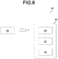
- a wireless communication system 95 includes the wireless communication device 90 and a second wireless communication device 96.
- the second wireless communication device 96 is configured to perform wireless communication with the wireless communication device 90.
- the configuration according to the present disclosure is not limited to some embodiments described above, and various modifications and changes can be made.
- the functions included in the components may be rearranged without logical contradiction, and a plurality of components may be combined into one or may be divided.
- the patch antenna is employed as the antenna element 11.
- the antenna to be employed as the antenna element 11 is not limited to the patch antenna. Other antennas may be employed as the antenna element 11.
- the antenna elements 11 may be arranged in the same orientation.
- two adjacent antenna elements 11 may be arranged in different orientations. When the two adjacent antenna elements 11 are arranged in different orientations, the antenna elements 11 are excited in the same direction.
- the terms “first”, “second”, “third” and so on are examples of identifiers meant to distinguish the configurations from each other.
- the respective identifying numbers can be reciprocally replaced with each other.
- the identifiers "first” and “second” can be reciprocally exchanged. The exchange of identifiers is performed simultaneously. Even after exchanging the identifiers, the configurations remain distinguished from each other. Identifiers may be removed. The configurations from which the identifiers are removed are still distinguishable by the reference numerals.
- the first feeding line 51 may be denoted as feeding line 51.
- the terms "first”, "second” and so on of the identifiers should not be used in the interpretation of the order of the configurations, or should not be used as the basis for having identifiers with low numbers, or should not be used as the basis for having identifiers with high numbers.
- the present disclosure includes a configuration in which the circuit board 70 includes the second feeding circuit 72 but does not include the first feeding circuit 71.
Landscapes
- Variable-Direction Aerials And Aerial Arrays (AREA)
- Waveguide Aerials (AREA)
Abstract
Description
- The present application claims the priority of
Japanese Patent Application No. 2018-207478 filed on November 2, 2018 - The present disclosure relates to an antenna, an array antenna, a wireless communication module, and a wireless communication device.
- In a method of changing a radiation pattern of an antenna, an external device such as a passive element needs to be placed near the antenna (e.g., Patent Literature 1). Placing the external device may lead to an increase in antenna size.
- Patent Literature 1:
Japanese Patent Application Laid-open No. 2016-139965 - An antenna according to an example of a plurality of embodiments of the present disclosure includes a radiation conductor, a ground conductor, a first feeding line, a second feeding line, and a connecting conductor. The first feeding line is electromagnetically connected to the radiation conductor and configured to excite the radiation conductor in a first direction. The second feeding line is electromagnetically connected to the radiation conductor and configured to excite the radiation conductor in a second direction. The connecting conductor is positioned apart from the center of the radiation conductor. The connecting conductor is spaced apart from the first feeding line by a first distance. The connecting conductor is spaced apart from the second feeding line by a second distance. The first distance is substantially equal to the second distance.
- An array antenna according to an example of a plurality of embodiments of the present disclosure includes a plurality of antenna elements that are a plurality of the antennas described above. The antenna elements are arranged in the first direction.
- A wireless communication module according to an example of a plurality of embodiments of the present disclosure includes the antenna element described above and a drive circuit. The drive circuit is configured to be directly or indirectly connected to each of the first feeding line and the second feeding line.
- A wireless communication module according to an example of a plurality of embodiments of the present disclosure includes the array antenna described above and a drive circuit. The drive circuit is configured to be directly or indirectly connected to each of the first feeding line and the second feeding line.
- A wireless communication device according to an example of a plurality of embodiments of the present disclosure includes the wireless communication module described above and a power source. The power source is configured to drive the drive circuit.
-
-
FIG. 1 is a perspective view illustrating an embodiment of an antenna. -
FIG. 2 is a cross-sectional view illustrating an embodiment of an antenna. -
FIG. 3 is a block diagram illustrating an embodiment of an antenna. -
FIG. 4 is a plan view illustrating an embodiment of a radiation conductor. -
FIG. 5 is a plan view illustrating an embodiment of an array antenna. -
FIG. 6 is a plan view illustrating an embodiment of a wireless communication module. -
FIG. 7 is a plan view illustrating an embodiment of a wireless communication device. -
FIG. 8 is a plan view illustrating an embodiment of a wireless communication system. - In conventional techniques, placing an external device may lead to an increase in antenna size.
- The present disclosure relates to providing an antenna, an array antenna, a wireless communication module, and a wireless communication device that are novel.
- Embodiments of the present disclosure will be described below.
- As illustrated in
FIG. 1 , anantenna 10 includes abase 20, aradiation conductor 30, aground conductor 40, a feeding line 50, a connectingconductor 60, and acircuit board 70. Thebase 20 is in contact with theradiation conductor 30, theground conductor 40, the feeding line 50, and the connectingconductor 60. Theradiation conductor 30, theground conductor 40, the feeding line 50, and the connectingconductor 60 are configured to function as anantenna element 11. Theantenna 10 is configured to oscillate at a predetermined resonance frequency and radiate electromagnetic waves. - The
base 20 may include any one of a ceramic material and a resin material as its composition. Examples of the ceramic material include, but are not limited to, sintered aluminum oxide, sintered aluminum nitride, sintered mullite, sintered glass ceramics, crystallized glass including a crystalline component deposited in a glass base material, sintered fine crystals such as mica or aluminum titanate, etc. Examples of the resin material include, but are not limited to, those obtained by curing uncured products such as epoxy resins, polyester resins, polyimide resins, polyamide-imide resins, polyetherimide resins, and liquid crystal polymers. - The
radiation conductor 30 and theground conductor 40 may include any of a metallic material, an alloy of a metallic material, a cured material of metal paste, and a conductive polymer as a composition. Theradiation conductor 30 and theground conductor 40 may be made of all the same materials. Theradiation conductor 30 and theground conductor 40 may be made of all the different materials. Theradiation conductor 30 and theground conductor 40 may include any combination of the same materials. Examples of the metal material include, but are not limited to, copper, silver, palladium, gold, platinum, aluminum, chromium, nickel, cadmium, lead, selenium, manganese, tin, vanadium, lithium, cobalt, titanium, etc. The alloy includes a plurality of metal materials. Examples of the metal paste include, but are not limited to, those obtained by mixing powder of a metal material with an organic solvent and a binder. Examples of the binder include, but are not limited to, epoxy resins, polyester resins, polyimide resins, polyamide-imide resins, polyetherimide resins, etc. Examples of the conductive polymer include, but are not limited to, polythiophene-based polymers, polyacethylene-based polymers, polyaniline-based polymers, polypyrrole-based polymers, etc. - The
radiation conductor 30 is configured to function as a resonator. Theradiation conductor 30 may be configured as a patch-type resonator. In an example, theradiation conductor 30 is positioned on thebase 20. In an example, theradiation conductor 30 is positioned at an end of thebase 20 in a z direction. In an example, theradiation conductor 30 may be positioned in thebase 20. A part of theradiation conductor 30 may be positioned inside thebase 20 and another part thereof may be positioned outside thebase 20. The surface of a part of theradiation conductor 30 may face the outside of thebase 20. - In an example of a plurality of embodiments, the
radiation conductor 30 extends along a first plane. Ends of theradiation conductor 30 are along a first direction and a second direction. The first direction and the second direction intersect each other. The first direction may be orthogonal to the second direction. In the present disclosure, the first direction (first axis) is denoted as an x direction. In the present disclosure, the second direction (third axis) is denoted as a y direction. In the present disclosure, a third direction (second axis) is denoted as the z direction. In the present disclosure, the first plane is denoted as an xy plane. In the present disclosure, a second plane is denoted as a yz plane. In the present disclosure, a third plane is denoted as a zx plane. These planes are planes in a coordinate space, and are not intended to indicate a particular plate or a particular surface. In the present disclosure, a surface integral in the xy plane may be referred to as first surface integral. In the present disclosure, a surface integral in the yz plane may be referred to as second surface integral. In the present disclosure, a surface integral in the zx plane may be referred to as third surface integral. The surface integral is represented by a unit such as square meter. In the present disclosure, a length in the x direction may be simply referred to as "length". In the present disclosure, a length in the y direction may be simply referred to as "width". In the present disclosure, a length in the z direction may be simply referred to as "height". - In an example of a plurality of embodiments, the
ground conductor 40 may be configured to function as the ground of theantenna element 11. In an example of a plurality of embodiments, theground conductor 40 extends along the first plane. Theground conductor 40 faces theradiation conductor 30 in the z direction. - The feeding line 50 may be configured to supply an electrical signal from the outside to the
antenna element 11. The feeding line 50 may be configured to supply an electrical signal from theantenna element 11 to the outside. The feeding line 50 may include afirst feeding line 51 and asecond feeding line 52. - Each of the
first feeding line 51 and thesecond feeding line 52 is electrically connected to theradiation conductor 30. Each of thefirst feeding line 51 and thesecond feeding line 52 only needs to be electromagnetically connected to theradiation conductor 30. In the present disclosure, "electromagnetic connection" includes electrical connection and magnetic connection. Thefirst feeding line 51 and thesecond feeding line 52 are in contact with different positions of theradiation conductor 30. As illustrated inFIG. 2 , theground conductor 40 has a plurality ofopenings 40a. Thefirst feeding line 51 and thesecond feeding line 52 individually pass through theopenings 40a of theground conductor 40. - The
first feeding line 51 is configured to contribute at least to supply of an electrical signal when theradiation conductor 30 resonates in the x direction. Thesecond feeding line 52 is configured to contribute at least to supply of an electrical signal when theradiation conductor 30 resonates in the y direction. Thefirst feeding line 51 and thesecond feeding line 52 are configured to excite theradiation conductor 30 in different directions. With this feeding line 50, theantenna 10 can reduce the excitation of theradiation conductor 30 in one direction during the excitation of theradiation conductor 30 in the other direction. - The connecting
conductor 60 is configured to electrically connect theradiation conductor 30 and theground conductor 40. A connection point between theradiation conductor 30 and the connectingconductor 60 serves as a potential reference of theradiation conductor 30 during resonance. The connectingconductor 60 extends along the z direction. - As illustrated in
FIG. 4 , the connectingconductor 60 is positioned apart from a center O of theradiation conductor 30 in the xy plane. The connectingconductor 60 is connected to a point different from the center O of theradiation conductor 30 in planar view of the xy plane. If the connectingconductor 60 is positioned at the center O of theradiation conductor 30, a change in current distribution due to the connection of the connectingconductor 60 is extremely small. In contrast, connecting the connectingconductor 60 to the point different from the center O of theradiation conductor 30 changes the potential reference. The current distribution changes by the change in potential reference. When the current distribution changes, a radiation pattern changes. With the connectingconductor 60 connected to the point different from the center O of theradiation conductor 30, theantenna 10 can change the radiation pattern. - The connecting
conductor 60 is spaced apart from thefirst feeding line 51 by a first distance d1. For example, the point where the connectingconductor 60 is connected to theradiation conductor 30 is spaced apart from a point where thefirst feeding line 51 is connected to theradiation conductor 30 by the first distance d1. The connectingconductor 60 is spaced apart from thesecond feeding line 52 by a second distance d2. For example, the point where the connectingconductor 60 is connected to theradiation conductor 30 is spaced apart from a point where thesecond feeding line 52 is connected to theradiation conductor 30 by the second distance d2. The first distance d1 is substantially equal to the second distance d2. - The connecting
conductor 60 may be spaced apart from thefirst feeding line 51 by a distance of 1/4 of an effective wavelength λ in the x direction. The connectingconductor 60 may be spaced apart from thesecond feeding line 52 by a distance of 1/4 of the effective wavelength λ in the y direction. - The
radiation conductor 30 may include a symmetry axis S that passes through the center O. The symmetry axis S passes through the center O and extends in a direction intersecting the x direction and the y direction. When theradiation conductor 30 is a square substantially parallel to the xy plane, the symmetry axis S may extend along a direction inclined at 45 degrees from a y-axis positive direction to an x-axis positive direction. Thefirst feeding line 51 and thesecond feeding line 52 are symmetric with respect to the symmetry axis S. For example, the point where thefirst feeding line 51 is connected to theradiation conductor 30 and the point where thesecond feeding line 52 is connected to theradiation conductor 30 may be line-symmetric with respect to the symmetry axis S. The connectingconductor 60 is positioned on the symmetry axis S. With the connectingconductor 60 positioned on the symmetry axis S, a change in a resonance direction of theradiation conductor 30 can be reduced. An effective adjustment range by the connectingconductor 60 may be a range in which a resonant electromagnetic field of 1/2 of the effective wavelength can be maintained. - A direction connecting the
first feeding line 51 and the connectingconductor 60 is inclined with respect to the x direction. Because thefirst feeding line 51 and the connectingconductor 60 are arranged to be inclined with respect to the x direction, thefirst feeding line 51 and the connectingconductor 60 can excite theradiation conductor 30 in the y direction as well. A direction connecting thesecond feeding line 52 and the connectingconductor 60 is inclined with respect to the y direction. Because thesecond feeding line 52 and the connectingconductor 60 are arranged to be inclined with respect to the y direction, thesecond feeding line 52 and the connectingconductor 60 can excite theradiation conductor 30 in the x direction as well. The excitation of theradiation conductor 30 in the two excitation directions causes impedance components in the respective directions to act on the feeding lines. Theantenna 10 may decrease an impedance at the time of input by canceling impedance components in the respective directions. By decreasing the impedance at the time of input, theantenna 10 may enhance isolation between two polarization directions. - As illustrated in
FIG. 3 , thecircuit board 70 includes afirst feeding circuit 71 and asecond feeding circuit 72. Thecircuit board 70 may include any one of thefirst feeding circuit 71 and thesecond feeding circuit 72. Thefirst feeding circuit 71 is configured to be electrically connected to thefirst feeding line 51. Thesecond feeding circuit 72 is configured to be electrically connected to thesecond feeding line 52. - As illustrated in
FIG. 5 , anarray antenna 12 includes a plurality ofantenna elements 11. Theantenna elements 11 may be aligned along the x direction. Theantenna elements 11 may be arranged in the x direction. Theantenna elements 11 may be aligned along the y direction. Theantenna elements 11 may be arranged in the y direction. Thearray antenna 12 includes at least onecircuit board 70. Thecircuit board 70 includes at least onefirst feeding circuit 71 and at least onesecond feeding circuit 72. Thearray antenna 12 includes at least onefirst feeding circuit 71 and at least onesecond feeding circuit 72. - The
first feeding circuit 71 may be connected to one ormore antenna elements 11. Thefirst feeding circuit 71 may be configured to supply the same signal to all theantenna elements 11 in feeding power to theantenna elements 11. Thefirst feeding circuit 71 may be configured to supply the same signal to thefirst feeding lines 51 of therespective antenna elements 11 in feeding power to theantenna elements 11. Thefirst feeding circuit 71 may be configured to supply signals of different phases to thefirst feeding lines 51 of therespective antenna elements 11 in feeding power to theantenna elements 11. - The
second feeding circuit 72 may be connected to one ormore antenna elements 11. Thesecond feeding circuit 72 may be configured to supply the same signal to all theantenna elements 11 in feeding power to theantenna elements 11. Thesecond feeding circuit 72 may be configured to supply the same signal to thesecond feeding lines 52 of therespective antenna elements 11 in feeding power to theantenna elements 11. Thesecond feeding circuit 72 may be configured to supply signals of different phases to thesecond feeding lines 52 of therespective antenna elements 11 in feeding power to theantenna elements 11. - As illustrated in
FIG. 6 , awireless communication module 80 includes adrive circuit 81. Thedrive circuit 81 is configured to drive theantenna element 11. Thedrive circuit 81 may be configured to feed a transmission signal to at least one of thefirst feeding circuit 71 and thesecond feeding circuit 72. Thedrive circuit 81 may be configured to receive a reception signal fed from at least one of thefirst feeding circuit 71 and thesecond feeding circuit 72. Thedrive circuit 81 may be configured to be directly or indirectly connected to each of thefirst feeding line 51 and thesecond feeding line 52. Thedrive circuit 81 may be configured to feed a transmission signal to at least one of thefirst feeding line 51 and thesecond feeding line 52. Thedrive circuit 81 may be configured to receive a reception signal fed from at least one of thefirst feeding line 51 and thesecond feeding line 52. Thedrive circuit 81 may be configured to feed a transmission signal to thefirst feeding line 51 and receive a reception signal fed from thesecond feeding line 52. - As illustrated in
FIG. 7 , awireless communication device 90 may include thewireless communication module 80, asensor 91, and abattery 92. Thesensor 91 is configured to perform sensing. Thebattery 92 is configured to supply power to any part of thewireless communication device 90. When configured to supply power to thedrive circuit 81 of thewireless communication module 80, thebattery 92 may be a power source configured to drive thedrive circuit 81. - As illustrated in
FIG. 8 , awireless communication system 95 includes thewireless communication device 90 and a secondwireless communication device 96. The secondwireless communication device 96 is configured to perform wireless communication with thewireless communication device 90. - The configuration according to the present disclosure is not limited to some embodiments described above, and various modifications and changes can be made. For example, the functions included in the components may be rearranged without logical contradiction, and a plurality of components may be combined into one or may be divided.
- The drawings that illustrate the configurations according to the present disclosure are schematic. The dimensional ratios and the like on the drawings do not necessarily match the actual ones.
- In some embodiments described above, the patch antenna is employed as the
antenna element 11. However, the antenna to be employed as theantenna element 11 is not limited to the patch antenna. Other antennas may be employed as theantenna element 11. - In the
array antenna 12, theantenna elements 11 may be arranged in the same orientation. In thearray antenna 12, twoadjacent antenna elements 11 may be arranged in different orientations. When the twoadjacent antenna elements 11 are arranged in different orientations, theantenna elements 11 are excited in the same direction. - In the present disclosure, the terms "first", "second", "third" and so on are examples of identifiers meant to distinguish the configurations from each other. In the present disclosure, regarding the configurations distinguished by the terms "first" and "second", the respective identifying numbers can be reciprocally replaced with each other. For example, regarding the first feeding line and the second feeding line, the identifiers "first" and "second" can be reciprocally exchanged. The exchange of identifiers is performed simultaneously. Even after exchanging the identifiers, the configurations remain distinguished from each other. Identifiers may be removed. The configurations from which the identifiers are removed are still distinguishable by the reference numerals. For example, the
first feeding line 51 may be denoted as feedingline 51. In the present disclosure, the terms "first", "second" and so on of the identifiers should not be used in the interpretation of the order of the configurations, or should not be used as the basis for having identifiers with low numbers, or should not be used as the basis for having identifiers with high numbers. The present disclosure includes a configuration in which thecircuit board 70 includes thesecond feeding circuit 72 but does not include thefirst feeding circuit 71. -
- 10
- ANTENNA
- 11
- ANTENNA ELEMENT
- 12
- ARRAY ANTENNA
- 20
- BASE
- 30
- RADIATION CONDUCTOR
- 40
- GROUND CONDUCTOR
- 40a
- OPENING
- 50
- FEEDING LINE
- 51
- FIRST FEEDING LINE
- 52
- SECOND FEEDING LINE
- 60
- CONNECTING CONDUCTOR
- 70
- CIRCUIT BOARD
- 71
- FIRST FEEDING CIRCUIT
- 72
- SECOND FEEDING CIRCUIT
- 80
- WIRELESS COMMUNICATION MODULE
- 81
- DRIVE CIRCUIT
- 90
- WIRELESS COMMUNICATION DEVICE
- 91
- SENSOR
- 92
- BATTERY
- 95
- WIRELESS COMMUNICATION SYSTEM
- 96
- SECOND WIRELESS COMMUNICATION DEVICE
Claims (13)
- An antenna comprising:a radiation conductor;a ground conductor;a first feeding line electromagnetically connected to the radiation conductor and configured to excite the radiation conductor in a first direction;a second feeding line electromagnetically connected to the radiation conductor and configured to excite the radiation conductor in a second direction; anda connecting conductor configured to electrically connect the radiation conductor to the ground conductor,the connecting conductorbeing positioned apart from a center of the radiation conductor,being spaced apart from the first feeding line by a first distance, andbeing spaced apart from the second feeding line by a second distance,the first distance being substantially equal to the second distance.
- The antenna according to claim 1, wherein
the first feeding line and the second feeding line are symmetric with respect to a symmetry axis that passes through the center of the radiation conductor. - The antenna according to claim 2, wherein
the connecting conductor is positioned on the symmetry axis. - The antenna according to any one of claims 1 to 3, wherein
the first direction is orthogonal to the second direction. - The antenna according to any one of claims 1 to 4, wherein
the first feeding line is positioned apart from the connecting conductor by a distance of 1/4 of an effective wavelength in the first direction. - The antenna according to any one of claims 1 to 5, wherein
the second feeding line is positioned apart from the connecting conductor by a distance of 1/4 of an effective wavelength in the second direction. - An array antenna comprising a plurality of antenna elements that are a plurality of the antennas according to any one of claims 1 to 6, wherein
the antenna elements are arranged in the first direction. - The array antenna according to claim 7, wherein
the antenna elements are arranged in the first direction and the second direction. - A wireless communication module comprising:the antenna element according to any one of claims 1 to 6; anda drive circuit configured to be directly or indirectly connected to each of the first feeding line and the second feeding line.
- The wireless communication module according to claim 9, wherein
the drive circuit is configured to feed a transmission signal to the first feeding line and receive a reception signal fed from the second feeding line. - A wireless communication module comprising:the array antenna according to claim 7 or 8; anda drive circuit configured to be directly or indirectly connected to each of the first feeding line and the second feeding line.
- The wireless communication module according to claim 11, wherein
the drive circuit is configured to feed a transmission signal to at least one of the first feeding line and the second feeding line and receive a reception signal fed from at least one of the first feeding line and the second feeding line. - A wireless communication device comprising:the wireless communication module according to any one of claims 9 to 12; anda power source configured to drive the drive circuit.
Applications Claiming Priority (2)
| Application Number | Priority Date | Filing Date | Title |
|---|---|---|---|
| JP2018207478 | 2018-11-02 | ||
| PCT/JP2019/042425 WO2020090837A1 (en) | 2018-11-02 | 2019-10-29 | Antenna, array antenna, radio communication module, and radio communication equipment |
Publications (2)
| Publication Number | Publication Date |
|---|---|
| EP3876343A1 true EP3876343A1 (en) | 2021-09-08 |
| EP3876343A4 EP3876343A4 (en) | 2022-07-27 |
Family
ID=70463236
Family Applications (1)
| Application Number | Title | Priority Date | Filing Date |
|---|---|---|---|
| EP19877951.4A Withdrawn EP3876343A4 (en) | 2018-11-02 | 2019-10-29 | ANTENNA, GROUP AERIAL, RADIO COMMUNICATIONS MODULE AND RADIO COMMUNICATIONS EQUIPMENT |
Country Status (5)
| Country | Link |
|---|---|
| US (1) | US11942691B2 (en) |
| EP (1) | EP3876343A4 (en) |
| JP (1) | JP7122389B2 (en) |
| CN (1) | CN113039682A (en) |
| WO (1) | WO2020090837A1 (en) |
Families Citing this family (3)
| Publication number | Priority date | Publication date | Assignee | Title |
|---|---|---|---|---|
| JP2769481B2 (en) | 1992-10-09 | 1998-06-25 | 株式会社大建 | Existing pile pulling casing device |
| EP3993161A4 (en) * | 2019-06-25 | 2023-07-26 | Kyocera Corporation | Antenna, wireless communication module, and wireless communication device |
| WO2025204559A1 (en) * | 2024-03-28 | 2025-10-02 | シャープ株式会社 | Signal processing device |
Family Cites Families (13)
| Publication number | Priority date | Publication date | Assignee | Title |
|---|---|---|---|---|
| JP4031253B2 (en) * | 2002-01-31 | 2008-01-09 | 三菱電機株式会社 | Antenna device |
| CN1862881B (en) * | 2005-05-11 | 2011-09-28 | 日立电线株式会社 | Distributed phase type circular polarized wave antenna, high-frequency module, and portable radio apparatus |
| CN103441339B (en) * | 2006-04-27 | 2016-01-13 | 泰科电子服务有限责任公司 | Metamaterial antenna equipment |
| JP2008207762A (en) * | 2007-02-28 | 2008-09-11 | Matsushita Electric Ind Co Ltd | In-vehicle machine |
| US7825867B2 (en) | 2007-04-26 | 2010-11-02 | Round Rock Research, Llc | Methods and systems of changing antenna polarization |
| JP2008301364A (en) * | 2007-06-01 | 2008-12-11 | Sanyo Electric Co Ltd | Antenna system, and wireless apparatus |
| US9742077B2 (en) * | 2011-03-15 | 2017-08-22 | Intel Corporation | Mm-wave phased array antenna with beam tilting radiation pattern |
| KR101988382B1 (en) * | 2013-03-29 | 2019-06-12 | 삼성전자주식회사 | Antenna device and electronic device with the same |
| JP6562628B2 (en) | 2014-12-11 | 2019-08-21 | 日本無線株式会社 | Target identification system |
| JP6335808B2 (en) | 2015-01-28 | 2018-05-30 | 三菱電機株式会社 | ANTENNA DEVICE AND ARRAY ANTENNA DEVICE |
| US20170110787A1 (en) * | 2015-10-14 | 2017-04-20 | Apple Inc. | Electronic Devices With Millimeter Wave Antennas And Metal Housings |
| US10594019B2 (en) * | 2016-12-03 | 2020-03-17 | International Business Machines Corporation | Wireless communications package with integrated antenna array |
| CN106935963A (en) * | 2017-01-20 | 2017-07-07 | 西南电子技术研究所(中国电子科技集团公司第十研究所) | High isolation dual polarized circumferential weld microband antenna unit |
-
2019
- 2019-10-29 CN CN201980072988.3A patent/CN113039682A/en active Pending
- 2019-10-29 US US17/290,774 patent/US11942691B2/en active Active
- 2019-10-29 EP EP19877951.4A patent/EP3876343A4/en not_active Withdrawn
- 2019-10-29 WO PCT/JP2019/042425 patent/WO2020090837A1/en not_active Ceased
- 2019-10-29 JP JP2020553949A patent/JP7122389B2/en active Active
Also Published As
| Publication number | Publication date |
|---|---|
| CN113039682A (en) | 2021-06-25 |
| EP3876343A4 (en) | 2022-07-27 |
| WO2020090837A1 (en) | 2020-05-07 |
| JP7122389B2 (en) | 2022-08-19 |
| US11942691B2 (en) | 2024-03-26 |
| JPWO2020090837A1 (en) | 2020-05-07 |
| US20210384644A1 (en) | 2021-12-09 |
Similar Documents
| Publication | Publication Date | Title |
|---|---|---|
| US11862878B2 (en) | Antenna, array antenna, radio communication module, and radio communication device | |
| US11831076B2 (en) | Antenna, wireless communication module, and wireless communication device | |
| US11916294B2 (en) | Antenna, wireless communication module, and wireless communication device | |
| US11942691B2 (en) | Antenna, array antenna, wireless communication module, and wireless communication device | |
| EP3817148B1 (en) | Antenna element, array antenna, communication unit, mobile body, and base station | |
| WO2020090838A1 (en) | Antenna, array antenna, wireless communication module, and wireless communication device | |
| JP7102593B2 (en) | Antennas, wireless communication modules and wireless communication devices | |
| US11784402B2 (en) | Antenna, wireless communication module, and wireless communication device | |
| EP3843009B1 (en) | Rfid tag substrate, rfid tag, and rfid system | |
| US12160055B2 (en) | Antenna, wireless communication module, and wireless communication device | |
| EP3796468A1 (en) | Wireless communication bolt, wireless communication nut, wireless communication washer, wireless communication rivet, wireless communication fastener, and structure | |
| EP3745536A1 (en) | Relay device | |
| CN116896825A (en) | Edge-enabled void structure |
Legal Events
| Date | Code | Title | Description |
|---|---|---|---|
| STAA | Information on the status of an ep patent application or granted ep patent |
Free format text: STATUS: THE INTERNATIONAL PUBLICATION HAS BEEN MADE |
|
| PUAI | Public reference made under article 153(3) epc to a published international application that has entered the european phase |
Free format text: ORIGINAL CODE: 0009012 |
|
| STAA | Information on the status of an ep patent application or granted ep patent |
Free format text: STATUS: REQUEST FOR EXAMINATION WAS MADE |
|
| 17P | Request for examination filed |
Effective date: 20210503 |
|
| AK | Designated contracting states |
Kind code of ref document: A1 Designated state(s): AL AT BE BG CH CY CZ DE DK EE ES FI FR GB GR HR HU IE IS IT LI LT LU LV MC MK MT NL NO PL PT RO RS SE SI SK SM TR |
|
| DAV | Request for validation of the european patent (deleted) | ||
| DAX | Request for extension of the european patent (deleted) | ||
| REG | Reference to a national code |
Ref country code: DE Ref legal event code: R079 Free format text: PREVIOUS MAIN CLASS: H01Q0001240000 Ipc: H01Q0009040000 |
|
| A4 | Supplementary search report drawn up and despatched |
Effective date: 20220624 |
|
| RIC1 | Information provided on ipc code assigned before grant |
Ipc: H01Q 21/06 20060101ALI20220620BHEP Ipc: H01Q 21/24 20060101ALI20220620BHEP Ipc: H01Q 21/08 20060101ALI20220620BHEP Ipc: H01Q 1/52 20060101ALI20220620BHEP Ipc: H01Q 9/04 20060101AFI20220620BHEP |
|
| P01 | Opt-out of the competence of the unified patent court (upc) registered |
Effective date: 20230505 |
|
| STAA | Information on the status of an ep patent application or granted ep patent |
Free format text: STATUS: THE APPLICATION HAS BEEN WITHDRAWN |
|
| 18W | Application withdrawn |
Effective date: 20240709 |