EP3871448B1 - Schaltung zur aufbereitung eines wake-up-signals - Google Patents
Schaltung zur aufbereitung eines wake-up-signals Download PDFInfo
- Publication number
- EP3871448B1 EP3871448B1 EP19795523.0A EP19795523A EP3871448B1 EP 3871448 B1 EP3871448 B1 EP 3871448B1 EP 19795523 A EP19795523 A EP 19795523A EP 3871448 B1 EP3871448 B1 EP 3871448B1
- Authority
- EP
- European Patent Office
- Prior art keywords
- circuit
- signal
- wake
- channel
- criterion
- Prior art date
- Legal status (The legal status is an assumption and is not a legal conclusion. Google has not performed a legal analysis and makes no representation as to the accuracy of the status listed.)
- Active
Links
Images

Classifications
-
- H—ELECTRICITY
- H04—ELECTRIC COMMUNICATION TECHNIQUE
- H04W—WIRELESS COMMUNICATION NETWORKS
- H04W52/00—Power management, e.g. Transmission Power Control [TPC] or power classes
- H04W52/02—Power saving arrangements
- H04W52/0209—Power saving arrangements in terminal devices
- H04W52/0225—Power saving arrangements in terminal devices using monitoring of external events, e.g. the presence of a signal
- H04W52/0229—Power saving arrangements in terminal devices using monitoring of external events, e.g. the presence of a signal where the received signal is a wanted signal
-
- F—MECHANICAL ENGINEERING; LIGHTING; HEATING; WEAPONS; BLASTING
- F02—COMBUSTION ENGINES; HOT-GAS OR COMBUSTION-PRODUCT ENGINE PLANTS
- F02D—CONTROLLING COMBUSTION ENGINES
- F02D41/00—Electrical control of supply of combustible mixture or its constituents
- F02D41/02—Circuit arrangements for generating control signals
-
- G—PHYSICS
- G01—MEASURING; TESTING
- G01R—MEASURING ELECTRIC VARIABLES; MEASURING MAGNETIC VARIABLES
- G01R19/00—Arrangements for measuring currents or voltages or for indicating presence or sign thereof
- G01R19/165—Indicating that current or voltage is either above or below a predetermined value or within or outside a predetermined range of values
- G01R19/16566—Circuits and arrangements for comparing voltage or current with one or several thresholds and for indicating the result not covered by subgroups G01R19/16504, G01R19/16528, G01R19/16533
- G01R19/16576—Circuits and arrangements for comparing voltage or current with one or several thresholds and for indicating the result not covered by subgroups G01R19/16504, G01R19/16528, G01R19/16533 comparing DC or AC voltage with one threshold
-
- H—ELECTRICITY
- H04—ELECTRIC COMMUNICATION TECHNIQUE
- H04W—WIRELESS COMMUNICATION NETWORKS
- H04W52/00—Power management, e.g. Transmission Power Control [TPC] or power classes
- H04W52/02—Power saving arrangements
- H04W52/0209—Power saving arrangements in terminal devices
- H04W52/0225—Power saving arrangements in terminal devices using monitoring of external events, e.g. the presence of a signal
- H04W52/0245—Power saving arrangements in terminal devices using monitoring of external events, e.g. the presence of a signal according to signal strength
-
- H—ELECTRICITY
- H04—ELECTRIC COMMUNICATION TECHNIQUE
- H04W—WIRELESS COMMUNICATION NETWORKS
- H04W52/00—Power management, e.g. Transmission Power Control [TPC] or power classes
- H04W52/02—Power saving arrangements
- H04W52/0209—Power saving arrangements in terminal devices
- H04W52/0261—Power saving arrangements in terminal devices managing power supply demand, e.g. depending on battery level
- H04W52/0274—Power saving arrangements in terminal devices managing power supply demand, e.g. depending on battery level by switching on or off the equipment or parts thereof
- H04W52/028—Power saving arrangements in terminal devices managing power supply demand, e.g. depending on battery level by switching on or off the equipment or parts thereof switching on or off only a part of the equipment circuit blocks
-
- Y—GENERAL TAGGING OF NEW TECHNOLOGICAL DEVELOPMENTS; GENERAL TAGGING OF CROSS-SECTIONAL TECHNOLOGIES SPANNING OVER SEVERAL SECTIONS OF THE IPC; TECHNICAL SUBJECTS COVERED BY FORMER USPC CROSS-REFERENCE ART COLLECTIONS [XRACs] AND DIGESTS
- Y02—TECHNOLOGIES OR APPLICATIONS FOR MITIGATION OR ADAPTATION AGAINST CLIMATE CHANGE
- Y02D—CLIMATE CHANGE MITIGATION TECHNOLOGIES IN INFORMATION AND COMMUNICATION TECHNOLOGIES [ICT], I.E. INFORMATION AND COMMUNICATION TECHNOLOGIES AIMING AT THE REDUCTION OF THEIR OWN ENERGY USE
- Y02D30/00—Reducing energy consumption in communication networks
- Y02D30/50—Reducing energy consumption in communication networks in wire-line communication networks, e.g. low power modes or reduced link rate
-
- Y—GENERAL TAGGING OF NEW TECHNOLOGICAL DEVELOPMENTS; GENERAL TAGGING OF CROSS-SECTIONAL TECHNOLOGIES SPANNING OVER SEVERAL SECTIONS OF THE IPC; TECHNICAL SUBJECTS COVERED BY FORMER USPC CROSS-REFERENCE ART COLLECTIONS [XRACs] AND DIGESTS
- Y02—TECHNOLOGIES OR APPLICATIONS FOR MITIGATION OR ADAPTATION AGAINST CLIMATE CHANGE
- Y02D—CLIMATE CHANGE MITIGATION TECHNOLOGIES IN INFORMATION AND COMMUNICATION TECHNOLOGIES [ICT], I.E. INFORMATION AND COMMUNICATION TECHNOLOGIES AIMING AT THE REDUCTION OF THEIR OWN ENERGY USE
- Y02D30/00—Reducing energy consumption in communication networks
- Y02D30/70—Reducing energy consumption in communication networks in wireless communication networks
Definitions
- the invention is based on a circuit for processing a wake-up signal.
- ASIC application-specific integrated circuit
- discrete circuits are usually developed either as part of an application-specific integrated circuit (ASIC) or as discrete circuits. The latter can be divided into analog and digital solutions.
- the task of such a circuit for processing a wake-up signal is to check the validity of the signals at the input of the circuit, which are used to activate or wake up electrical devices, such as control devices. This means that only signals with a certain amplitude or time duration are recognized as valid. This means that only in the case of a valid wake-up signal will a corresponding wake-up request or a corresponding processed wake-up signal be output to the subsequent electrical devices. If the applied wake-up signal is not recognized as valid, the electrical devices will not be activated.
- the known circuits for processing a wake-up signal have fixed and unchangeable parameters for the specified criteria for checking the applied wake-up signal. Furthermore, these circuits cannot be switched off or deactivated or require additional protective elements in order to be able to be connected directly to wake-up lines in a vehicle. Also included These circuits typically have a comparator that activates or wakes up the subsequent electrical devices when a certain threshold is exceeded.
- a method for waking up the power of a remotely managed digital display which comprises the following steps: providing a detector for detecting an envelope of a digital signal. Receiving an expandable length packet consisting of the same, repeated data symbol. detecting that the extended length packet has been received by the detector to provide an output signal, comparing the output signal to a reference threshold and providing a wake-up signal if the output signal exceeds the reference threshold. Information can then be received, which can be displayed on the remotely managed digital display.
- a wake-up circuit which is configured to detect a wake-up signal from a wireless terminal, the wake-up signal including a modulated waveform signal.
- a switchable communication module is provided, which is configured to be switched from a sleep mode, in which the communication module cannot be operated for communication with the wireless terminal, to an active mode based on a control signal which is generated by the wake-up circuit, in which the communication module can be operated for communication with the wireless terminal.
- a wireless terminal includes a first wireless communication interface configured to communicate with a device using a wireless communication protocol, a second wireless communication interface configured to wirelessly communicate with a wireless access node of a wireless network, and a processor that configures is to support the forwarding of information between the terminal device and the wireless access node of the wireless network.
- the circuit includes an evaluation circuit, which checks the validity of an applied wake-up signal, and an output driver circuit, which outputs a processed wake-up signal if the evaluation circuit evaluates the applied wake-up signal as valid.
- the evaluation circuit includes a comparator which compares the applied wake-up signal with at least one threshold value for evaluation.
- the evaluation circuit includes an input circuit and a switchable constant voltage source, via which at least one criterion for evaluating the applied wake-up signal can be set, the comparator being designed as a multi-channel integrated comparator circuit.
- the individual channels of the integrated comparator circuit each evaluate a criterion of the applied wake-up signal, with the multi-channel integrated comparator circuit comprising an internal voltage source which generates a reference voltage.
- a first voltage signal present at the input of a first channel of the multi-channel integrated comparator circuit is compared with the reference voltage, with a first criterion being met if the first voltage signal is greater than the reference voltage.
- a second voltage signal present at the input of a second channel of the multi-channel integrated comparator circuit is compared with the reference voltage, with a second criterion being met if the second voltage signal is greater than the reference voltage.
- the circuit for processing a wake-up signal with the features of independent claim 1 has the advantage that through the use of a multi-channel integrated comparator circuit, a discrete input circuit and a switchable discrete constant voltage source, input parameters of the circuit, such as an input impedance, and criteria for Evaluation of the applied wake-up signal can be easily adjusted by varying the component values in the input circuit and/or in the constant voltage source.
- these input parameters and criteria for use in motor vehicles can be specified very precisely and stably over a wide voltage and temperature range. This is caused by the high input resistance of the multi-channel integrated comparator circuit, through which a high-resistance decoupling of the line of the wake-up signal from the rest of the circuit can be achieved.
- embodiments of the circuit according to the invention for processing a wake-up signal in the idle state are completely inactive except for the multi-channel integrated comparator circuit and are therefore characterized by a very low power consumption, which is suitable for permanently powered systems.
- the use of the multi-channel integrated comparator circuit enables a relatively compact design of the circuit because only a few external components are required. The use of a permanently active and regulated power supply or a clock source is not necessary.
- Embodiments of the present invention provide a circuit for processing a wake-up signal that can be used to activate electrical devices.
- the circuit for processing a wake-up signal includes an evaluation circuit, which checks the validity of an applied wake-up signal, and an output driver circuit, which outputs a processed wake-up signal when the evaluation circuit detects the applied wake-up signal. Signal assessed as valid.
- the evaluation circuit includes a comparator which compares the applied wake-up signal with at least one threshold value for evaluation.
- the evaluation circuit includes an input circuit and a switchable constant voltage source, via which at least one criterion is used to evaluate the applied voltage Wake-up signal can be adjusted, the comparator being designed as a multi-channel integrated comparator circuit, and the individual channels of the integrated comparator circuit each evaluating a criterion of the applied wake-up signal.
- the multi-channel integrated comparator circuit includes an internal voltage source which generates a reference voltage.
- a first voltage signal present at the input of a first channel of the multi-channel integrated comparator circuit which represents the amplitude of the applied wake-up signal, is compared with the reference voltage, the first criterion being met if the first voltage signal is greater than the reference voltage.
- the divided wake-up signal can be present at the non-inverting input of the first channel and the internal reference voltage can be present at an internal inverting input of the first channel, which is preferably not accessible from the outside in order to reduce the number of connection pins on the integrated comparator circuit .
- a second voltage signal present at the input of a second channel of the multi-channel integrated comparator circuit which represents the duration of the applied wake-up signal, is compared with the reference voltage, the second criterion being met if the second voltage signal is greater than the reference voltage .
- the output signal of the constant voltage source present across the at least one capacitor of the RC circuit can be present as a second voltage signal at the inverting input of the second channel and the internal reference voltage can be present at an internal non-inverting input of the second channel, which is preferably not accessible from the outside to reduce the number of connection pins on the integrated comparator circuit.
- the multi-channel integrated comparator circuit changes a state at the output of the first channel when the first criterion is met, the change in state at the output of the first channel starting the evaluation of the second criterion.
- the output of the first channel can change its active “low” state to a “high Impedance” change state.
- This can be implemented, for example, by a so-called open collector output of the comparator.
- the at least one capacitor can be charged with the charging voltage via the charging resistor.
- the input circuit specifies a first criterion for evaluating an amplitude of the applied wake-up signal via an adjustable division ratio of a voltage divider.
- the input circuit can specify an input impedance of the evaluation circuit.
- the wake-up signal is first divided down by the voltage divider and freed from fast transient interference signals by using an additional filter capacitor.
- An amplitude detection threshold can be set as the first criterion using the adjustable division ratio of the voltage divider. By changing the division ratio, the amplitude detection threshold can be easily adapted to appropriate customer requirements.
- the switchable constant voltage source can specify a second criterion for evaluating a duration of the applied wake-up signal via an adjustable time constant of an RC circuit.
- the applied wake-up signal can switch on the constant voltage source.
- the time constant of the RC circuit as a second criterion can simply be changed the value of a charging resistor and/or at least one capacitor of the RC circuit can be adapted to appropriate customer requirements.
- a charging voltage of the at least one capacitor of the RC circuit can be stabilized to a predetermined value of, for example, 2.7V, for example by a Zener diode.
- the multi-channel integrated comparator circuit can change a state at the output of the second channel when the second criterion is met, wherein the change in state at the output of the second channel can activate the output driver circuit.
- the output of the second channel can change its "high impedance" state to an active "low” state. Since an open collector output is also used here, the output of the second channel is pulled to ground potential. This change in state of the output of the second channel activates the output driver circuit so that it outputs the processed wake-up signal, which activates or wakes up subsequent electrical devices.
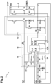
- the illustrated embodiment of a circuit 1 according to the invention for processing a wake-up signal WUP includes an evaluation circuit 10, which checks the validity of an applied wake-up signal WUP, and a Output driver circuit 5, which outputs a processed wake-up signal WUPA when the evaluation circuit 10 evaluates the applied wake-up signal WUP as valid.
- the evaluation circuit 10 includes a comparator 12, which compares the applied wake-up signal WUP with at least one threshold value for evaluation.
- the evaluation circuit 10 comprises an input circuit 14 and a switchable constant voltage source 16, via which at least one criterion for evaluating the applied wake-up signal WUP can be set.
- the comparator 12 is designed as a multi-channel integrated comparator circuit 12A, with the individual channels of the integrated comparator circuit 12A each evaluating a criterion of the applied wake-up signal WUP.
- the input circuit 14 specifies a first criterion for evaluating an amplitude of the applied wake-up signal WUP via an adjustable division ratio of a voltage divider ST.
- the input circuit 14 specifies an input impedance of the evaluation circuit 10 by appropriately dimensioning the individual ohmic resistors R1 and R2 of the voltage divider ST.
- the switchable constant voltage source 16 specifies a second criterion for evaluating a duration of the applied wake-up signal WUP via an adjustable time constant of an RC circuit RL, C1, C2.
- the applied wake-up signal WUP switches on the constant voltage source 16 via an ohmic resistor RB, which in the illustrated embodiment is connected to a base of a switching transistor T1.
- the comparator 12 is designed as a two-channel integrated comparator circuit 12A, which includes an unspecified internal voltage source and whose outputs Out_A and Out_B are designed as so-called open collector outputs.
- the internal voltage source generated a reference voltage of, for example, 400mV.
- a first voltage signal present at the input In_A of the first channel of the multi-channel integrated comparator circuit 12A which represents the amplitude of the applied wake-up signal WUP, is compared with the reference voltage, the first criterion being met if the first voltage signal is greater than that Reference voltage is.
- a second voltage signal present at the input ln_B of the second channel of the multi-channel integrated comparator circuit 12A which represents the duration of the applied wake-up signal WUP, is compared with the reference voltage, a time criterion being met as a second criterion when the second voltage signal is greater than the reference voltage.
- the applied wake-up signal WUP is first divided down by the voltage divider ST of the input circuit 14 and freed from fast transient interference signals by using a filter capacitor CF.
- An amplitude detection threshold is set as the first criterion for evaluating the wake-up signal WUP via the division ratio of the voltage divider ST of the input circuit 14 and can be easily adapted to corresponding customer requirements by changing the values of the two ohmic resistors R1, R2.
- the divided wake-up signal WUP is connected to a non-inverting input In_A of the first channel.
- the internal voltage source is connected to an inverting input of the first channel, which is not accessible from the outside. If the divided wake-up signal WUP or the first voltage signal at the non-inverting input In_A of the first channel of the two-channel integrated comparator circuit 12A exceeds the internal reference voltage of 400 mV, a predetermined amplitude criterion of the wake-up signal WUP is met and an output Out_A of the The first channel of the two-channel integrated comparator circuit 12A changes its state from active “Low” to “High Impedance”. As a result, the capacitors C1 and C2 of the RC circuit, which are connected to the output Out_A of the first channel via an ohmic protective resistor RS, are charged via a charging resistor RL of the RC circuit.
- the RC circuit in the exemplary embodiment shown comprises two capacitors C1 and C2 connected in parallel.
- the voltage across the capacitors C1 and C2 is simultaneously present as a second voltage signal at an inverting input In_B of the second channel of the two-channel integrated comparator circuit 12A.
- the internal voltage source is connected to a non-inverting input of the second channel, which is not accessible from the outside is. If the second voltage signal reaches the internal reference voltage of 400mV, then in addition to the amplitude criterion, the time criterion is met and the output Out_B of the second channel of the two-channel integrated comparator circuit 12A changes its state from "High Impedance" to active "Low".
- the output driver circuit 5 pulls a connection pin of the output Out_B of the second channel to ground potential. If the wake-up signal WUP is no longer present at the evaluation circuit 10 or the amplitude criterion is no longer met, then the output Out_A of the first channel of the two-channel integrated comparator circuit 12A changes its state from "High Impedance” to active “Low", so that the two capacitors C1 and C2 can be quickly discharged via the protective resistor RS and this output Out_A. This behavior prevents the possible “adding up” of the charges in the two capacitors C1 and C2 in the event of several consecutive wake-up signals, which are only separated from each other by short pauses.
- the time criterion can easily be adapted to appropriate customer requirements by changing the time constant via the values of the two capacitors C1 and C2 and the charging resistor RL.
- Fig. 2 It can also be seen that the charging voltage of the capacitors C1 and C2 is stabilized to, for example, 2.7V by a Zener diode Z1 and an ohmic resistor R5.
- another voltage stabilization can be used in the constant voltage source 16 to charge the capacitors C1 and C2.
- a balanced band-gap voltage reference can be used instead of the Zener diode Z1 if a higher accuracy of the time criterion is required.
- it is only switched on via the switching transistor T1 when a wake-up signal WUP is actually present at the input of the evaluation circuit 10.
- the energy for charging the capacitors C1 and C2 only comes from a continuous supply with reverse polarity protection VZP is taken from a vehicle battery, not shown, when a wake-up signal WUP is present. In this way, extensive decoupling of the wake-up signal WUP is possible, which enables a constant and supply-independent impedance of the input of the evaluation circuit 10.
- the processed wake-up signal WUPA at the output of the output driver circuit 5 is brought approximately to the potential of a supply voltage VDD via a driver transistor T2 and an ohmic resistor R8.
- the driver transistor T2 is controlled by the active "low" state of the output Out_B of the second channel of the two-channel integrated comparator circuit 12A, with an operating point of the driver transistor T2 being adjustable via a base voltage divider made up of two ohmic resistors R6 and R7.
- a supply connection VDD of the comparator circuit 12A is connected via a protection circuit 5, which limits the supply voltage VDD of the two-channel integrated comparator circuit 12A and the output driver circuit 5.
- the protective circuit 3 comprises two series-connected ohmic resistors R3 and R4 and a further Zener diode Z2, which separates the supply voltage VDD from the polarity-protected continuous supply VZP of the vehicle.
- a downstream low pass TP which comprises an ohmic resistor RT and a capacitor CT, additionally filters the supply voltage VDD of the two-channel integrated comparator circuit 12A with an adjustable corner frequency of, for example, 600 Hz in order to keep interference away from the two-channel integrated comparator circuit 12A and thus optimizing the quality of the wake-up signal discrimination according to amplitude and time.
Landscapes
- Engineering & Computer Science (AREA)
- Computer Networks & Wireless Communication (AREA)
- Signal Processing (AREA)
- Power Engineering (AREA)
- Physics & Mathematics (AREA)
- General Physics & Mathematics (AREA)
- Chemical & Material Sciences (AREA)
- Combustion & Propulsion (AREA)
- Mechanical Engineering (AREA)
- General Engineering & Computer Science (AREA)
- Logic Circuits (AREA)
- Manipulation Of Pulses (AREA)
Description
- Die Erfindung geht aus von einer Schaltung zur Aufbereitung eines Wake-Up-Signals.
- Aus dem Stand der Technik bekannte Schaltungen zur Aufbereitung eines sogenannten Wake-Up-Signals werden in der Regel entweder als Bestandteil einer anwendungsspezifischen integrierten Schaltung (ASIC) oder als diskrete Schaltungen entwickelt. Die letzteren lassen sich in analoge und digitale Lösungen unterteilen. Die Aufgabe einer solchen Schaltung zur Aufbereitung eines Wake-Up-Signals besteht darin, die Signale am Eingang der Schaltung auf Gültigkeit zu prüfen, welche zum Aktivieren bzw. Aufwecken von elektrischen Geräten, wie beispielsweise Steuergeräte verwendet werden. So werden nur Signale mit einer bestimmten Amplitude bzw. zeitlichen Dauer als gültig erkannt. Das bedeutet, dass nur im Falle eines gültigen Wake-Up-Signals eine korrespondierende Weckanforderung bzw. ein korrespondierendes aufbereitetes Wake-Up-Signal an die nachfolgende elektrischen Geräte ausgegeben werden. Wird also das anliegende Wake-Up-Signal nicht als gültig erkannt, dann werden die elektrischen Geräte nicht aktiviert.
- Die bekannten Schaltungen zur Aufbereitung eines Wake-Up-Signals besitzen fest eingestellte und unveränderbare Parameter für die vorgegebenen Kriterien zur Überprüfung des anliegenden Wake-Up-Signals. Ferner lassen sich diese Schaltungen nicht abschalten bzw. deaktivieren oder benötigen zusätzliche Schutzelemente, um in einem Fahrzeug direkt an Wake-Up-Leitungen angeschlossen werden zu können. Zudem enthalten diese Schaltungen typischerweise einen Komparator, der beim Überschreiten einer bestimmten Schwelle die nachfolgenden elektrischen Geräte aktiviert bzw. aufweckt.
- Aus der
US 2011/0317601 A1 ist ein Verfahren zum Aufwecken der Stromversorgung einer fernverwalteten Digitalanzeige bekannt, welches nachfolgende Schritte umfasst: Bereitstellen eines Detektors zum Erfassen einer Hüllkurve eines digitalen Signals. Empfangen eines Pakets mit erweiterbarer Länge, welches aus einem gleichen, wiederholten Datensymbol besteht. Erkennen, dass das Paket mit erweiterter Länge vom Detektor empfangen wurde, um ein Ausgangssignal bereitzustellen, wobei das Ausgangssignal mit einer Referenzschwelle verglichen wird und ein Aufwecksignal bereitgestellt wird, wenn das Ausgangssignal die Referenzschwelle überschreitet. Anschließend können Informationen empfangen werden, welche auf der fernverwalteten Digitalanzeige angezeigt werden können. - Aus der
US 9,565,633 B2 - Aus der
WO 2017/083831 A1 ist eine Schaltung zur Aufbereitung eines Wake-Up-Signals bekannt, welches zur Aktivierung von elektrischen Geräten verwendbar ist. Die Schaltung umfasst eine Bewertungsschaltung, welche ein anliegendes Wake-Up-Signal auf seine Gültigkeit überprüft, und eine Ausgangstreiberschaltung, welche ein aufbereitetes Wake-Up-Signal ausgibt, wenn die Bewertungsschaltung das anliegende Wake-Up-Signal als gültig bewertet. Die Bewertungsschaltung umfasst einen Komparator, welcher das anliegende Wake-Up-Signal zur Bewertung mit mindestens einem Schwellwert vergleicht. Zudem umfasst die Bewertungsschaltung eine Eingangsschaltung und eine schaltbare Konstantspannungsquelle, über welche jeweils mindestens ein Kriterium zur Bewertung des anliegenden Wake-Up-Signals einstellbar ist, wobei der Komparator als mehrkanalige integrierte Komparatorschaltung ausgeführt ist. Die einzelnen Kanäle der integrierten Komparatorschaltung bewerten jeweils ein Kriterium des anliegenden Wake-Up-Signals, wobei die mehrkanalige integrierte Komparatorschaltung eine interne Spannungsquelle umfasst, welche eine Referenzspannung erzeugt. Ein am Eingang eines ersten Kanals der mehrkanaligen integrierten Komparatorschaltung anliegendes erstes Spannungssignal wird mit der Referenzspannung verglichen, wobei ein erstes Kriterium erfüllt ist, wenn das erste Spannungssignals größer als die Referenzspannung ist. Ein am Eingang eines zweiten Kanals der mehrkanaligen integrierten Komparatorschaltung anliegendes zweites Spannungssignal wird mit der Referenzspannung verglichen, wobei ein zweites Kriterium erfüllt ist, wenn das zweite Spannungssignal größer als die Referenzspannung ist. - Die Schaltung zur Aufbereitung eines Wake-Up-Signals mit den Merkmalen des unabhängigen Patentanspruchs 1 hat den Vorteil, dass durch den Einsatz einer mehrkanaligen integrierten Komparatorschaltung, einer diskreten Eingangsschaltung und einer schaltbaren diskreten Konstantspannungsquelle Eingangsparameter der Schaltung, wie beispielsweise eine Eingangsimpedanz, und Kriterien zur Bewertung des anliegenden Wake-Up-Signals durch die Variation der Bauteilwerte in der Eingangsschaltung und/oder in der Konstantspannungsquelle einfach eingestellt werden können. Zudem können diese Eingangsparameter und Kriterien für einen Einsatz in Kraftfahrzeugen sehr präzise und stabil über einen weiten Spannungs- und Temperaturbereich vorgegeben werden. Dies wird durch den hohen Eingangswiderstand der mehrkanaligen integrierten Komparatorschaltung bewirkt, durch welchen eine hochohmige Entkopplung der Leitung des Wake-Up-Signals von der restlichen Schaltung erreicht werden kann. Damit lässt sich ein sehr weites Spektrum an Kundenanforderungen abdecken, ohne dass eine Überarbeitung des Layouts der Schaltung notwendig wäre. Zudem kann die Spannungsversorgung der Konstantspannungsquelle nur bei einem tatsächlich anliegenden Wake-Up-Signal zugeschaltet werden. Dadurch sind Ausführungsformen der erfindungsgemä-ßen Schaltung zur Aufbereitung eines Wake-Up-Signals im Ruhezustand bis auf die mehrkanaligen integrierte Komparatorschaltung komplett inaktiv und zeichnen sich deswegen durch einen sehr niedrigen, für dauerversorgte Systeme geeigneten Stromverbrauch aus. Der Einsatz der mehrkanaligen integrierten Komparatorschaltung ermöglicht einen relativ kompakten Aufbau der Schaltung, da nur wenige externe Bauteile benötigt werden. Der Einsatz einer permanent aktiven und geregelten Spannungsversorgung sowie einer Taktquelle ist nicht erforderlich.
- Ausführungsformen der vorliegenden Erfindung stellen eine Schaltung zur Aufbereitung eines Wake-Up-Signals zur Verfügung, welches zur Aktivierung von elektrischen Geräten verwendbar ist. Die Schaltung zur Aufbereitung eines Wake-Up-Signals umfasst eine Bewertungsschaltung, welche ein anliegendes Wake-Up-Signal auf seine Gültigkeit überprüft, und eine Ausgangstreiberschaltung, welche ein aufbereitetes Wake-Up-Signal ausgibt, wenn die Bewertungsschaltung das anliegende Wake-Up-Signal als gültig bewertet. Die Bewertungsschaltung umfasst einen Komparator, welcher das anliegende Wake-Up-Signal zur Bewertung mit mindestens einem Schwellwert vergleicht. Hierbei umfasst die Bewertungsschaltung eine Eingangsschaltung und eine schaltbare Konstantspannungsquelle, über welche jeweils mindestens ein Kriterium zur Bewertung des anliegenden Wake-Up-Signals einstellbar ist, wobei der Komparator als mehrkanalige integrierte Komparatorschaltung ausgeführt ist, und wobei die einzelnen Kanäle der integrierten Komparatorschaltung jeweils ein Kriterium des anliegenden Wake-Up-Signals bewerten.
- Hierbei umfasst die mehrkanalige integrierte Komparatorschaltung eine interne Spannungsquelle, welche eine Referenzspannung erzeugt. Zudem wird ein am Eingang eines ersten Kanals der mehrkanaligen integrierten Komparatorschaltung anliegendes erstes Spannungssignal, welches die Amplitude des anliegenden Wake-Up-Signals repräsentiert, mit der Referenzspannung verglichen, wobei das erste Kriterium erfüllt ist, wenn das erste Spannungssignals größer als die Referenzspannung ist. Hierbei kann das heruntergeteilte Wake-Up-Signal am nichtinvertierenden Eingang des ersten Kanals anliegen und die interne Referenzspannung kann an einem internen invertierenden Eingang des ersten Kanals anliegen, welcher vorzugsweise von außen nicht zugänglich ist, um die Anzahl von Anschlusspins an der integrierten Komparatorschaltung zu reduzieren. Des Weiteren wird ein am Eingang eines zweiten Kanals der mehrkanaligen integrierten Komparatorschaltung anliegendes zweites Spannungssignal, welches die Zeitdauer des anliegenden Wake-Up-Signals repräsentiert, mit der Referenzspannung verglichen, wobei das zweite Kriterium erfüllt ist, wenn das zweite Spannungssignal größer als die Referenzspannung ist. Hierbei kann das über dem mindestens einen Kondensator der RC-Schaltung anliegende Ausgangssignal der Konstantspannungsquelle als zweites Spannungssignal am invertierenden Eingang des zweiten Kanals anliegen und die interne Referenzspannung kann an einem internen nichtinvertierenden Eingang des zweiten Kanals anliegen, welcher vorzugsweise von außen nicht zugänglich ist, um die Anzahl von Anschlusspins an der integrierten Komparatorschaltung zu reduzieren.
- Des Weiteren ändert die mehrkanalige integrierte Komparatorschaltung einen Zustand am Ausgang des ersten Kanals, wenn das erste Kriterium erfüllt ist, wobei die Zustandsänderung am Ausgang des ersten Kanals die Bewertung des zweiten Kriteriums startet. So kann der Ausgang des ersten Kanals beispielsweise seinen aktiven "Low" Zustand in einen "High Impedance" Zustand ändern. Dies kann beispielsweise durch einen sogenannten Open-Kollektor-Ausgang des Komparators umgesetzt werden. Durch den Zustandswechsel des Ausgangs des ersten Kanals kann der mindestens eine Kondensator über den Ladewiderstand mit der Ladespannung aufgeladen werden.
- Durch die in den abhängigen Ansprüchen aufgeführten Maßnahmen und Weiterbildungen sind vorteilhafte Verbesserungen der im unabhängigen Patentanspruch 1 angegebenen Schaltung zur Aufbereitung eines Wake-Up-Signals möglich.
- Besonders vorteilhaft ist, dass die Eingangsschaltung über ein einstellbares Teilungsverhältnis eines Spannungsteilers ein erstes Kriterium zur Bewertung einer Amplitude des anliegenden Wake-Up-Signals vorgibt. Zudem kann die Eingangsschaltung eine Eingangsimpedanz der Bewertungsschaltung vorgeben. Durch den Spannungsteiler wird das Wake-Up-Signal zunächst heruntergeteilt und durch Verwendung eines zusätzlichen Filterkondensators on schnellen transienten Störsignalen befreit. Über das einstellbare Teilungsverhältnis des Spannungsteilers kann eine Amplitudenerkennungsschwelle als erstes Kriterium eingestellt werden. Durch das Verändern des Teilungsverhältnisses kann die Amplitudenerkennungsschwelle einfach an entsprechende Kundenanforderungen angepasst werden. Durch geeignete Wahl des Innenwiderstandes der Eingangsschaltung, welcher sich aus den Werten der Widerstände des Spannungsteilers ergibt, zusammen mit dem Kapazitätswert des Filterkondensators können transiente Störungen, welche eine stabile Amplitudenerkennung erschweren, beseitigt werden.
- In vorteilhafter Ausgestaltung der Schaltung kann die schaltbare Konstantspannungsquelle über eine einstellbare Zeitkonstante einer RC-Schaltung ein zweites Kriterium zur Bewertung einer Zeitdauer des anliegenden Wake-Up-Signals vorgeben. Zudem kann das anliegende Wake-Up-Signal die Konstantspannungsquelle einschalten. Die Zeitkonstante der RC-Schaltung als zweites Kriterium kann einfach durch Verändern des Wertes eines Ladewiderstands und/oder mindestens eines Kondensators der RC-Schaltung an entsprechende Kundenanforderungen angepasst werden. Um eine Unabhängigkeit des zweiten Kriteriums von der Spannungsversorgung der Schaltung zu gewährleisten, kann eine Ladespannung des mindestens einen Kondensators der RC-Schaltung beispielsweise durch eine Zenerdiode auf einen vorgegebenen Wert von beispielsweise 2,7V stabilisiert werden. Um einen permanenten Stromverbrauch der Konstantspannungsquelle zu verhindern, wird diese beispielsweise über einen Transistor nur dann zugeschaltet, wenn tatsächlich ein Wake-Up-Signal am Eingang der Bewertungsschaltung anliegt. Dies ermöglicht eine Reduzierung des Ruhestromverbrauchs der Schaltung auf wenige Mikroampere. Da die Energie zum Aufladen des mindestens einen Kondensators nur dann aus der Energiequelle des Fahrzeugs entnommen wird, wenn ein gültiges Wake-Up-Signal vorliegt. Auf diese Weise ist eine weitgehende Entkopplung des Wake-Up-Signals möglich, was eine konstante und versorgungsunabhängige Impedanz des Eingangs der Schaltung ermöglicht. Damit eignet sich Ausführungsformen der erfindungsgemäßen Schaltung für Sleep Systeme die an einer Dauerversorgung angeschlossen sind und im schlafenden Zustand, d.h. im nicht aktiven Zustand, Stromanforderungen von weniger als 100µA erfüllen müssen.
- In weiterer vorteilhafter Ausgestaltung der Schaltung kann die mehrkanalige integrierte Komparatorschaltung einen Zustand am Ausgang des zweiten Kanals ändern, wenn das zweite Kriterium erfüllt ist, wobei die Zustandsänderung am Ausgang des zweiten Kanals die Ausgangstreiberschaltung aktivieren kann. So kann der Ausgang des zweiten Kanals beispielsweise seinen "High Impedance" Zustand auf einen aktiv "Low" Zustand ändern. Da auch hier ein Open-Kollektor-Ausgang verwendet wird, wird der Ausgang des zweiten Kanals auf Massepotential gezogen. Durch diesen Zustandswechsel des Ausgangs des zweiten Kanals wird die Ausgangstreiberschaltung aktiviert, so dass diese das aufbereitete Wake-Up-Signal ausgibt, welches nachfolgende elektrische Geräte aktiviert bzw. aufweckt.
- Ein Ausführungsbeispiel der Erfindung ist in der Zeichnung dargestellt und wird in der nachfolgenden Beschreibung näher erläutert. In der Zeichnung bezeichnen gleiche Bezugszeichen Komponenten bzw. Elemente, die gleiche bzw. analoge Funktionen ausführen.
- Kurze Beschreibung der Zeichnungen
-
Fig. 1 zeigt eine schematische Blockdiagramm eines Ausführungsbeispiels einer erfindungsgemäßen Schaltung zur Aufbereitung eines Wake-Up-Signals. -
Fig. 2 zeigt ein Schaltbild der erfindungsgemäßen Schaltung zur Aufbereitung eines Wake-Up-Signals ausFig. 1 . - Wie aus
Fig. 1 und2 ersichtlich ist, umfasst das dargestellte Ausführungsbeispiel einer erfindungsgemäßen Schaltung 1 zur Aufbereitung eines Wake-Up-Signals WUP, welches zur Aktivierung von elektrischen Geräten verwendbar ist, eine Bewertungsschaltung 10, welche ein anliegendes Wake-Up-Signal WUP auf seine Gültigkeit überprüft, und eine Ausgangstreiberschaltung 5, welche ein aufbereitetes Wake-Up-Signal WUPA ausgibt, wenn die Bewertungsschaltung 10 das anliegende Wake-Up-Signal WUP als gültig bewertet. Die Bewertungsschaltung 10 umfasst einen Komparator 12, welcher das anliegende Wake-Up-Signal WUP zur Bewertung mit mindestens einem Schwellwert vergleicht. Hierbei umfasst die Bewertungsschaltung 10 eine Eingangsschaltung 14 und eine schaltbare Konstantspannungsquelle 16, über welche jeweils mindestens ein Kriterium zur Bewertung des anliegenden Wake-Up-Signals WUP einstellbar ist. Zudem ist der Komparator 12 als mehrkanalige integrierte Komparatorschaltung 12A ausgeführt, wobei die einzelnen Kanäle der integrierten Komparatorschaltung 12A jeweils ein Kriterium des anliegenden Wake-Up-Signals WUP bewerten. - Im dargestellten Ausführungsbeispiel gibt die Eingangsschaltung 14 über ein einstellbares Teilungsverhältnis eines Spannungsteilers ST ein erstes Kriterium zur Bewertung einer Amplitude des anliegenden Wake-Up-Signals WUP vor. Zudem gibt die Eingangsschaltung 14 über eine entsprechende Dimensionierung der einzelnen ohmschen Widerstände R1 und R2 des Spannungsteilers ST eine Eingangsimpedanz der Bewertungsschaltung 10 vor. Die schaltbare Konstantspannungsquelle 16 gibt über eine einstellbare Zeitkonstante einer RC-Schaltung RL, C1, C2 ein zweites Kriterium zur Bewertung einer Zeitdauer des anliegenden Wake-Up-Signals WUP vor.
- Wie aus
Fig. 1 und2 weiter ersichtlich ist, schaltet das anliegende Wake-Up-Signal WUP die Konstantspannungsquelle 16 über einen ohmschen Widerstand RB ein, welcher im dargestellten Ausführungsbeispiel mit einer Basis eines Schalttransistors T1 verbunden ist. - Im dargestellten Ausführungsbeispiel ist der Komparator 12 als zweikanalige integrierte Komparatorschaltung 12A ausgeführt, welche eine nicht näher bezeichnete interne Spannungsquelle umfasst und dessen Ausgänge Out_A und Out_B als sogenannte Open-Kollektor-Ausgänge ausgeführt sind. Die interne Spannungsquelle erzeugte eine Referenzspannung von beispielsweise 400mV. Hierbei wird ein am Eingang In_A des ersten Kanals der mehrkanaligen integrierte Komparatorschaltung 12A anliegendes erstes Spannungssignal, welches die Amplitude des anliegenden Wake-Up-Signals WUP repräsentiert, mit der Referenzspannung verglichen, wobei das erste Kriterium erfüllt ist, wenn das erste Spannungssignals größer als die Referenzspannung ist. Des Weiteren wird ein am Eingang ln_B des zweiten Kanals der mehrkanaligen integrierte Komparatorschaltung 12A anliegendes zweites Spannungssignal, welches die Zeitdauer des anliegenden Wake-Up-Signals WUP repräsentiert, mit der Referenzspannung verglichen, wobei ein Zeitkriterium als zweites Kriterium erfüllt ist, wenn das zweite Spannungssignal größer als die Referenzspannung ist.
- Wie aus
Fig. 2 weiter ersichtlich ist, wird das anliegende Wake-Up-Signal WUP zunächst vom Spannungsteiler ST der Eingangsschaltung 14 heruntergeteilt und durch Verwendung eines Filterkondensators CF von schnellen transienten Störsignalen befreit. Über das Teilungsverhältnis des Spannungsteilers ST der Eingangsschaltung 14 wird eine Amplitudenerkennungsschwelle als erstes Kriterium zur Bewertung des Wake-Up-Signals WUP eingestellt und kann durch das Verändern der Werte der beiden ohmschen Widerstände R1, R2 leicht an entsprechende Kundenanforderungen angepasst werden. Durch geeignete Wahl des Innenwiderstandes der Eingangsschaltung zusammen mit dem Kapazitätswert des Filterkondensators CF können transiente Störungen, welche eine stabile Amplitudenerkennung erschweren, beseitigt werden. Das heruntergeteilte Wake-Up-Signal WUP ist mit einem nichtinvertierenden Eingang In_A des ersten Kanals verbunden. Die interne Spannungsquelle ist mit einem invertierenden Eingang des ersten Kanals verbunden, welcher nicht von au-ßen zugänglich ist. Überschreitet das heruntergeteilte Wake-Up-Signal WUP bzw. das erste Spannungssignal am nichtinvertierenden Eingang In_A des ersten Kanals der zweikanaligen integrierten Komparatorschaltung 12A die interne Referenzspannung von 400mV, so wird ein vorgegebenes Amplitudenkriterium des Wake-Up-Signals WUP erfüllt und ein Ausgang Out_A des ersten Kanals der zweikanaligen integrierten Komparatorschaltung 12A wechselt seinen Zustand von aktiv "Low" auf "High Impedance". Dadurch werden die über einen ohmschen Schutzwiderstand RS mit dem Ausgang Out_A des ersten Kanals verbundenen Kondensatoren C1 und C2 der RC-Schaltung über einen Ladewiderstand RL der RC-Schaltung aufgeladen. - Wie aus
Fig. 2 weiter ersichtlich ist, umfasst die RC-Schaltung im dargestellten Ausführungsbeispiel zwei parallel geschaltete Kondensatoren C1 und C2. Die Spannung über den Kondensatoren C1 und C2 liegt gleichzeitig als zweites Spannungssignal an einem invertierenden Eingang In_B des zweiten Kanals der zweikanaligen integrierten Komparatorschaltung 12A an. Die interne Spannungsquelle ist mit einem nichtinvertierenden Eingang des zweiten Kanals verbunden, welcher nicht von außen zugänglich ist. Erreicht das zweite Spannungssignal die interne Referenzspannung von 400mV, dann ist zusätzlich zum Amplitudenkriterium das Zeitkriterium erfüllt und der Ausgang Out_B des zweiten Kanals der zweikanaligen integrierten Komparatorschaltung 12A wechselt seinen Zustand von "High Impedance" auf aktiv "Low". Da auch hier ein Open-Kollektor-Ausgang verwendet wird, zieht die Ausgangstreiberschaltung 5 einen Anschlusspin des Ausgangs Out_B des zweiten Kanals auf Massepotential. Liegt das Wake-Up-Signal WUP nicht mehr an der Bewertungsschaltung 10 an bzw. wird das Amplitudenkriterium nicht mehr erfüllt, dann wechselt der Ausgang Out_A des ersten Kanals der zweikanaligen integrierten Komparatorschaltung 12A seinen Zustand von "High Impedance" auf aktiv "Low", so dass die beiden Kondensatoren C1 und C2 über den Schutzwiderstand RS und diesen Ausgang Out_A schnell entladen werden können. Dieses Verhalten verhindert das mögliche "Aufaddieren" der Ladungen in den beiden Kondensatoren C1 und C2 bei mehreren aufeinander folgenden Wake-Up-Signalen, welche nur durch kurze Pausen voneinander getrennt sind. Das Zeitkriterium kann leicht durch eine Veränderung der Zeitkonstante über die Werte der beiden Kondensatoren C1 und C2 und des Ladewiderstands RL auf entsprechende Kundenanforderungen angepasst werden. - Wie aus
Fig. 2 weiter ersichtlich ist, wird die Ladespannung der Kondensatoren C1 und C2 durch eine Zenerdiode Z1 und einen ohmschen Widerstand R5 auf beispielsweise 2,7V stabilisiert. Alternativ kann in der Konstantspannungsquelle 16 eine andere Spannungsstabilisierung zum Laden der Kondensatoren C1 und C2 verwendet werden. So kann beispielsweise eine abgeglichene Band-Gap-Spannungsreferenz anstatt der Zenerdiode Z1 verwendet werden, falls eine höhere Genauigkeit des Zeitkriteriums gefordert wird. Um einen permanenten Stromverbrauch der Konstantspannungsquelle 16 zu verhindern, wird diese über den Schalttransistor T1 nur dann zugeschaltet, wenn tatsächlich ein Wake-Up-Signal WUP am Eingang der Bewertungsschaltung 10 anliegt. Dies ermöglicht eine Reduzierung des Ruhestromverbrauchs der Bewertungsschaltung 10 auf wenige Mikroampere. Die Energie zum Aufladen der Kondensatoren C1 und C2 wird nur dann aus einer verpolgeschützten Dauerversorgung VZP einer nicht dargestellten Fahrzeugbatterie entnommen, wenn ein Wake-Up-Signal WUP anliegt. Auf diese Weise ist eine weitgehende Entkopplung des Wake-Up-Signals WUP möglich, was eine konstante und versorgungsunabhängige Impedanz des Eingangs der Bewertungsschaltung 10 ermöglicht. - Ist sowohl das Amplitudenkriterium als auch Zeitkriterium erfüllt, dann wird das aufbereitete Wake-Up-Signal WUPA am Ausgang der Ausgangstreiberschaltung 5 über einen Treibertransistor T2 und einen ohmschen Widerstand R8 annähernd auf das Potential einer Versorgungsspannung VDD gebracht. Dabei wird der Treibertransistor T2 durch den aktiven "Low" Zustand des Ausgangs Out_B des zweiten Kanals der zweikanaligen integrierten Komparatorschaltung 12A angesteuert, wobei ein Arbeitspunkt des Treibertransistors T2 über einen Basisspannungsteiler aus zwei ohmschen Widerständen R6 und R7 einstellbar ist.
- Zur optimalen Versorgung der zweikanaligen integrierten Komparatorschaltung 12A erfolgt eine Anbindung eines Versorgungsanschlusses VDD der Komparatorschaltung 12A über eine Schutzschaltung 5, welche die Versorgungsspannung VDD der zweikanaligen integrierten Komparatorschaltung 12A und der Ausgangstreiberschaltung 5 begrenzt. Die Schutzschaltung 3 umfasst im dargestellten Ausführungsbeispiel zwei in Reihe geschaltete ohmsche Widerstände R3 und R4 und eine weitere Zenerdiode Z2, welche die Versorgungsspannung VDD aus der verpolgeschützten Dauerversorgung VZP des Fahrzeugs abklammert. Im üblichen Spannungsbereich bei abgestelltem Fahrzeug (Motor aus) der Dauerversorgung VZP im Bereich von 5V bis 13,8V wird nahezu kein Strom durch die Schutzschaltung 3 nach Masse abgeführt und damit hat auch dieser Schaltungsteil keinen Einfluss auf die Sleep Stromanforderungen für die verpolgeschützte Dauerversorgung VZP des Fahrzeugs. Ein nachgeschalteter Tiefpass TP, welcher einen ohmschen Widerstand RT und einen Kondensator CT umfasst, filtert zusätzlich die Versorgungsspannung VDD der zweikanaligen integrierten Komparatorschaltung 12A mit einer einstellbaren Eckfrequenz von beispielsweise 600Hz, um Störungen von der zweikanaligen integrierten Komparatorschaltung 12A fernzuhalten und damit die Güte der Wake-Up-Signaldiskriminierung nach Amplitude und Zeit zu optimieren.
Claims (6)
- Schaltung (1) zur Aufbereitung eines Wake-Up-Signals (WUP), welches zur Aktivierung von elektrischen Geräten verwendbar ist, mit einer Bewertungsschaltung (10), welche ein anliegendes Wake-Up-Signal (WUP) auf seine Gültigkeit überprüft, und einer Ausgangstreiberschaltung (5), welche ein aufbereitetes Wake-Up-Signal (WUPA) ausgibt, wenn die Bewertungsschaltung (10) das anliegende Wake-Up-Signal (WUP) als gültig bewertet, wobei die Bewertungsschaltung (10) einen Komparator (12) umfasst, welcher das anliegende Wake-Up-Signal (WUP) zur Bewertung mit mindestens einem Schwellwert vergleicht, wobei die Bewertungsschaltung (10) eine Eingangsschaltung (14) und eine schaltbare Konstantspannungsquelle (16) umfasst, über welche jeweils mindestens ein Kriterium zur Bewertung des anliegenden Wake-Up-Signals (WUP) einstellbar ist, wobei der Komparator (12) als mehrkanalige integrierte Komparatorschaltung (12A) ausgeführt ist, wobei die einzelnen Kanäle der integrierten Komparatorschaltung (12A) jeweils ein Kriterium des anliegenden Wake-Up-Signals (WUP) bewerten, wobei die mehrkanalige integrierte Komparatorschaltung (12A) eine interne Spannungsquelle umfasst, welche eine Referenzspannung erzeugt, wobei ein am Eingang (In_A) eines ersten Kanals der mehrkanaligen integrierten Komparatorschaltung (12A) anliegendes erstes Spannungssignal, welches die Amplitude des anliegenden Wake-Up-Signals (WUP) repräsentiert, mit der Referenzspannung verglichen wird, wobei ein erstes Kriterium erfüllt ist, wenn das erste Spannungssignals größer als die Referenzspannung ist, und wobei ein am Eingang (ln_B) eines zweiten Kanals der mehrkanaligen integrierten Komparatorschaltung (12A) anliegendes zweites Spannungssignal, welches die Zeitdauer des anliegenden Wake-Up-Signals (WUP) repräsentiert, mit der Referenzspannung verglichen wird, wobei ein zweites Kriterium erfüllt ist, wenn das zweite Spannungssignal größer als die Referenzspannung ist, dadurch gekennzeichnet, dass die mehrkanalige integrierte Komparatorschaltung (12A) einen Zustand am Ausgang (Out_A) des ersten Kanals ändert, wenn das erste Kriterium erfüllt ist, und wobei die Zustandsänderung am Ausgang (Out_A) des ersten Kanals die Bewertung des zweiten Kriteriums startet.
- Schaltung (1) nach Anspruch 1, dadurch gekennzeichnet, dass die Eingangsschaltung (14) über ein einstellbares Teilungsverhältnis eines Spannungsteilers (ST) das erste Kriterium zur Bewertung einer Amplitude des anliegenden Wake-Up-Signals (WUP) vorgibt.
- Schaltung (1) nach Anspruch 1 oder 2, dadurch gekennzeichnet, dass die Eingangsschaltung (14) eine Eingangsimpedanz der Bewertungsschaltung (10) vorgibt.
- Schaltung (1) nach einem der Ansprüche 1 bis 3, dadurch gekennzeichnet, dass die schaltbare Konstantspannungsquelle (16) über eine einstellbare Zeitkonstante einer RC-Schaltung (RL, C1, C2) das zweite Kriterium zur Bewertung einer Zeitdauer des anliegenden Wake-Up-Signals (WUP) vorgibt.
- Schaltung (1) nach Anspruch 4, dadurch gekennzeichnet, dass das anliegende Wake-Up-Signal (WUP) die Konstantspannungsquelle (16) einschaltet.
- Schaltung (1) nach einem der Ansprüche 1 bis 5, dadurch gekennzeichnet, dass die mehrkanalige integrierte Komparatorschaltung (12A) einen Zustand am Ausgang (Out_B) des zweiten Kanals ändert, wenn das zweite Kriterium erfüllt ist, wobei die Zustandsänderung am Ausgang (Out_B) des zweiten Kanals die Ausgangstreiberschaltung (5) aktiviert.
Applications Claiming Priority (2)
| Application Number | Priority Date | Filing Date | Title |
|---|---|---|---|
| DE102018218171.3A DE102018218171A1 (de) | 2018-10-24 | 2018-10-24 | Schaltung zur Aufbereitung eines Wake-Up-Signals |
| PCT/EP2019/079069 WO2020084074A1 (de) | 2018-10-24 | 2019-10-24 | Schaltung zur aufbereitung eines wake-up-signals |
Publications (2)
| Publication Number | Publication Date |
|---|---|
| EP3871448A1 EP3871448A1 (de) | 2021-09-01 |
| EP3871448B1 true EP3871448B1 (de) | 2023-12-06 |
Family
ID=68392982
Family Applications (1)
| Application Number | Title | Priority Date | Filing Date |
|---|---|---|---|
| EP19795523.0A Active EP3871448B1 (de) | 2018-10-24 | 2019-10-24 | Schaltung zur aufbereitung eines wake-up-signals |
Country Status (5)
| Country | Link |
|---|---|
| US (1) | US11849308B2 (de) |
| EP (1) | EP3871448B1 (de) |
| CN (1) | CN112913285B (de) |
| DE (1) | DE102018218171A1 (de) |
| WO (1) | WO2020084074A1 (de) |
Families Citing this family (3)
| Publication number | Priority date | Publication date | Assignee | Title |
|---|---|---|---|---|
| CN109982419B (zh) * | 2019-04-28 | 2024-03-12 | 成都天诚慧芯科技有限公司 | 一种无线唤醒电路 |
| CN117631637A (zh) * | 2022-08-15 | 2024-03-01 | 上海禾赛科技有限公司 | 用于激光雷达的休眠唤醒控制电路、方法以及激光雷达 |
| CN115940977B (zh) * | 2023-02-22 | 2023-06-02 | 上海芯浦科技有限公司 | 一种信号接收器唤醒电路 |
Family Cites Families (9)
| Publication number | Priority date | Publication date | Assignee | Title |
|---|---|---|---|---|
| AT413251B (de) * | 2003-12-09 | 2005-12-15 | Efkon Ag | Aufwecksignal-detektorschaltung |
| JP4779342B2 (ja) * | 2004-11-25 | 2011-09-28 | パナソニック電工株式会社 | 無線センサ装置 |
| CN101527467A (zh) * | 2009-04-03 | 2009-09-09 | 复旦大学 | 具有自动数字校正功能的唤醒电路 |
| US8374111B2 (en) * | 2010-06-28 | 2013-02-12 | Symbol Technologies, Inc. | Digital signage with on-demand power wake up |
| KR20120071947A (ko) * | 2010-12-23 | 2012-07-03 | 한국전자통신연구원 | 웨이크업 신호 통신 시스템, 장치 및 방법, 그리고 무선 단말기 |
| US9754202B2 (en) * | 2012-04-05 | 2017-09-05 | Ricoh Co., Ltd. | Low power radio frequency communication |
| EP3149872B1 (de) * | 2014-05-27 | 2018-03-28 | Koninklijke Philips N.V. | Körpergekoppelte kommunikationsvorrichtung mit synchronisierung |
| US9565633B2 (en) * | 2014-07-03 | 2017-02-07 | Alcatel Lucent | Opportunistic information forwarding using wireless terminals in the internet-of-things |
| JP6936543B2 (ja) * | 2015-11-13 | 2021-09-15 | テキサス インスツルメンツ インコーポレイテッド | Usbインターフェース回路および低電力動作のための方法 |
-
2018
- 2018-10-24 DE DE102018218171.3A patent/DE102018218171A1/de active Pending
-
2019
- 2019-10-24 EP EP19795523.0A patent/EP3871448B1/de active Active
- 2019-10-24 CN CN201980070097.4A patent/CN112913285B/zh active Active
- 2019-10-24 US US17/260,830 patent/US11849308B2/en active Active
- 2019-10-24 WO PCT/EP2019/079069 patent/WO2020084074A1/de not_active Ceased
Also Published As
| Publication number | Publication date |
|---|---|
| EP3871448A1 (de) | 2021-09-01 |
| US20210297953A1 (en) | 2021-09-23 |
| US11849308B2 (en) | 2023-12-19 |
| CN112913285A (zh) | 2021-06-04 |
| CN112913285B (zh) | 2024-02-27 |
| DE102018218171A1 (de) | 2020-04-30 |
| WO2020084074A1 (de) | 2020-04-30 |
Similar Documents
| Publication | Publication Date | Title |
|---|---|---|
| DE102009000697B4 (de) | Treiberschaltung für eine Zweidrahtleitung und Verfahren zum Erzeugen zweier Ausgangsströme für eine Zweidrahtleitung | |
| EP3871448B1 (de) | Schaltung zur aufbereitung eines wake-up-signals | |
| DE69937817T2 (de) | Aktive Hochziehschaltung für Open-Drain-Signale | |
| DE102011085419B4 (de) | Schaltung und Verfahren zur Zubehördetektion | |
| DE102021116198A1 (de) | Treiberschaltung für ein lokales verbindungsnetzwerk (lin) | |
| DE102017127047A1 (de) | Fahrzeug mit überwachungssystem mit mehrfachen analogschaltern bei simultaner schaltzustandserfassung | |
| EP2829929B1 (de) | Feldgerät mit einem trennbaren Anzeige- und/oder Bedienmodul | |
| EP0135121A1 (de) | Schaltungsanordnung zum Erzeugen von Rechtecksignalen | |
| WO2005015816A1 (de) | Verfahren und vorrichtung zur bidirektionalen eindraht-datenübertragung | |
| DE102011015498A1 (de) | Eingangsschaltung für eine Eingangsbaugruppe und Verfahren zum Betreiben einer Eingangsschaltung | |
| DE102005002679A1 (de) | Aufweck-Schaltungsanordnung und Steuerungsvorrichtung | |
| DE102018215696A1 (de) | Vorrichtung und Verfahren zum Erzeugen eines Wecksignals, und Ladeschnittstelle | |
| EP0461432A2 (de) | Vorrichtung zum Ein- und Ausschalten einer Last | |
| DE102015221848A1 (de) | Bussystem und Verfahren zur Diagnose eines Kurzschlusses | |
| DE102015115021A1 (de) | Taktüberwachung für sequentielle Logikschaltungen | |
| DE68917653T2 (de) | Eingangsschutzschaltung für eine Halbleitervorrichtung. | |
| EP2891179B1 (de) | Schutzschaltung und verfahren zum schutz einer schaltung | |
| DE112020005393T5 (de) | Kommunikationsvorrichtung und kommunikationssystem | |
| EP0666957B1 (de) | Elektromotorischer antrieb | |
| EP3521131A1 (de) | Sensor, system und verfahren zum erfassen von metallteilen | |
| DE69207493T2 (de) | Regler mit Messung der Spannung zwischen den Phasen in einem Drehstromgenerator | |
| EP3874282B1 (de) | Überspannungsschutzschaltung für ein steuergerät für ein fahrzeug, steuergerät für ein fahrzeug und verfahren zum testen einer überspannungsschutzschaltung für ein steuergerät für ein fahrzeug | |
| WO2005057388A1 (de) | Aufwecksignal-detektorschaltung | |
| CN108776265B (zh) | 动态阻抗电路及信号检测电路 | |
| EP1589437A2 (de) | Elektronische Schnittstellenschaltung und Bussystem mit der Schnittstellenschaltung |
Legal Events
| Date | Code | Title | Description |
|---|---|---|---|
| STAA | Information on the status of an ep patent application or granted ep patent |
Free format text: STATUS: UNKNOWN |
|
| STAA | Information on the status of an ep patent application or granted ep patent |
Free format text: STATUS: THE INTERNATIONAL PUBLICATION HAS BEEN MADE |
|
| PUAI | Public reference made under article 153(3) epc to a published international application that has entered the european phase |
Free format text: ORIGINAL CODE: 0009012 |
|
| STAA | Information on the status of an ep patent application or granted ep patent |
Free format text: STATUS: REQUEST FOR EXAMINATION WAS MADE |
|
| 17P | Request for examination filed |
Effective date: 20210525 |
|
| AK | Designated contracting states |
Kind code of ref document: A1 Designated state(s): AL AT BE BG CH CY CZ DE DK EE ES FI FR GB GR HR HU IE IS IT LI LT LU LV MC MK MT NL NO PL PT RO RS SE SI SK SM TR |
|
| DAV | Request for validation of the european patent (deleted) | ||
| DAX | Request for extension of the european patent (deleted) | ||
| REG | Reference to a national code |
Ref country code: DE Ref legal event code: R079 Free format text: PREVIOUS MAIN CLASS: H04W0052020000 Ipc: G01R0019165000 |
|
| RIC1 | Information provided on ipc code assigned before grant |
Ipc: H04W 52/02 20090101ALI20230728BHEP Ipc: G01R 19/165 20060101AFI20230728BHEP |
|
| GRAP | Despatch of communication of intention to grant a patent |
Free format text: ORIGINAL CODE: EPIDOSNIGR1 |
|
| STAA | Information on the status of an ep patent application or granted ep patent |
Free format text: STATUS: GRANT OF PATENT IS INTENDED |
|
| INTG | Intention to grant announced |
Effective date: 20230913 |
|
| GRAS | Grant fee paid |
Free format text: ORIGINAL CODE: EPIDOSNIGR3 |
|
| GRAA | (expected) grant |
Free format text: ORIGINAL CODE: 0009210 |
|
| STAA | Information on the status of an ep patent application or granted ep patent |
Free format text: STATUS: THE PATENT HAS BEEN GRANTED |
|
| RBV | Designated contracting states (corrected) |
Designated state(s): AL AT BE BG CH CY CZ DK EE ES FI FR GB GR HR HU IE IS IT LI LT LU LV MC MK MT NL NO PL PT RO RS SE SI SK SM TR |
|
| REG | Reference to a national code |
Ref country code: DE Ref legal event code: R108 |
|
| AK | Designated contracting states |
Kind code of ref document: B1 Designated state(s): AL AT BE BG CH CY CZ DK EE ES FI FR GB GR HR HU IE IS IT LI LT LU LV MC MK MT NL NO PL PT RO RS SE SI SK SM TR |
|
| REG | Reference to a national code |
Ref country code: GB Ref legal event code: FG4D Free format text: NOT ENGLISH |
|
| REG | Reference to a national code |
Ref country code: CH Ref legal event code: EP |
|
| REG | Reference to a national code |
Ref country code: IE Ref legal event code: FG4D Free format text: LANGUAGE OF EP DOCUMENT: GERMAN |
|
| REG | Reference to a national code |
Ref country code: LT Ref legal event code: MG9D |
|
| PG25 | Lapsed in a contracting state [announced via postgrant information from national office to epo] |
Ref country code: GR Free format text: LAPSE BECAUSE OF FAILURE TO SUBMIT A TRANSLATION OF THE DESCRIPTION OR TO PAY THE FEE WITHIN THE PRESCRIBED TIME-LIMIT Effective date: 20240307 |
|
| REG | Reference to a national code |
Ref country code: NL Ref legal event code: MP Effective date: 20231206 |
|
| PG25 | Lapsed in a contracting state [announced via postgrant information from national office to epo] |
Ref country code: LT Free format text: LAPSE BECAUSE OF FAILURE TO SUBMIT A TRANSLATION OF THE DESCRIPTION OR TO PAY THE FEE WITHIN THE PRESCRIBED TIME-LIMIT Effective date: 20231206 |
|
| PG25 | Lapsed in a contracting state [announced via postgrant information from national office to epo] |
Ref country code: ES Free format text: LAPSE BECAUSE OF FAILURE TO SUBMIT A TRANSLATION OF THE DESCRIPTION OR TO PAY THE FEE WITHIN THE PRESCRIBED TIME-LIMIT Effective date: 20231206 |
|
| PG25 | Lapsed in a contracting state [announced via postgrant information from national office to epo] |
Ref country code: LT Free format text: LAPSE BECAUSE OF FAILURE TO SUBMIT A TRANSLATION OF THE DESCRIPTION OR TO PAY THE FEE WITHIN THE PRESCRIBED TIME-LIMIT Effective date: 20231206 Ref country code: GR Free format text: LAPSE BECAUSE OF FAILURE TO SUBMIT A TRANSLATION OF THE DESCRIPTION OR TO PAY THE FEE WITHIN THE PRESCRIBED TIME-LIMIT Effective date: 20240307 Ref country code: ES Free format text: LAPSE BECAUSE OF FAILURE TO SUBMIT A TRANSLATION OF THE DESCRIPTION OR TO PAY THE FEE WITHIN THE PRESCRIBED TIME-LIMIT Effective date: 20231206 Ref country code: BG Free format text: LAPSE BECAUSE OF FAILURE TO SUBMIT A TRANSLATION OF THE DESCRIPTION OR TO PAY THE FEE WITHIN THE PRESCRIBED TIME-LIMIT Effective date: 20240306 |
|
| PG25 | Lapsed in a contracting state [announced via postgrant information from national office to epo] |
Ref country code: NL Free format text: LAPSE BECAUSE OF FAILURE TO SUBMIT A TRANSLATION OF THE DESCRIPTION OR TO PAY THE FEE WITHIN THE PRESCRIBED TIME-LIMIT Effective date: 20231206 |
|
| PG25 | Lapsed in a contracting state [announced via postgrant information from national office to epo] |
Ref country code: SE Free format text: LAPSE BECAUSE OF FAILURE TO SUBMIT A TRANSLATION OF THE DESCRIPTION OR TO PAY THE FEE WITHIN THE PRESCRIBED TIME-LIMIT Effective date: 20231206 Ref country code: RS Free format text: LAPSE BECAUSE OF FAILURE TO SUBMIT A TRANSLATION OF THE DESCRIPTION OR TO PAY THE FEE WITHIN THE PRESCRIBED TIME-LIMIT Effective date: 20231206 Ref country code: NO Free format text: LAPSE BECAUSE OF FAILURE TO SUBMIT A TRANSLATION OF THE DESCRIPTION OR TO PAY THE FEE WITHIN THE PRESCRIBED TIME-LIMIT Effective date: 20240306 Ref country code: NL Free format text: LAPSE BECAUSE OF FAILURE TO SUBMIT A TRANSLATION OF THE DESCRIPTION OR TO PAY THE FEE WITHIN THE PRESCRIBED TIME-LIMIT Effective date: 20231206 Ref country code: LV Free format text: LAPSE BECAUSE OF FAILURE TO SUBMIT A TRANSLATION OF THE DESCRIPTION OR TO PAY THE FEE WITHIN THE PRESCRIBED TIME-LIMIT Effective date: 20231206 Ref country code: HR Free format text: LAPSE BECAUSE OF FAILURE TO SUBMIT A TRANSLATION OF THE DESCRIPTION OR TO PAY THE FEE WITHIN THE PRESCRIBED TIME-LIMIT Effective date: 20231206 |
|
| PG25 | Lapsed in a contracting state [announced via postgrant information from national office to epo] |
Ref country code: IS Free format text: LAPSE BECAUSE OF FAILURE TO SUBMIT A TRANSLATION OF THE DESCRIPTION OR TO PAY THE FEE WITHIN THE PRESCRIBED TIME-LIMIT Effective date: 20240406 |
|
| PG25 | Lapsed in a contracting state [announced via postgrant information from national office to epo] |
Ref country code: CZ Free format text: LAPSE BECAUSE OF FAILURE TO SUBMIT A TRANSLATION OF THE DESCRIPTION OR TO PAY THE FEE WITHIN THE PRESCRIBED TIME-LIMIT Effective date: 20231206 |
|
| PG25 | Lapsed in a contracting state [announced via postgrant information from national office to epo] |
Ref country code: SK Free format text: LAPSE BECAUSE OF FAILURE TO SUBMIT A TRANSLATION OF THE DESCRIPTION OR TO PAY THE FEE WITHIN THE PRESCRIBED TIME-LIMIT Effective date: 20231206 |
|
| PG25 | Lapsed in a contracting state [announced via postgrant information from national office to epo] |
Ref country code: SM Free format text: LAPSE BECAUSE OF FAILURE TO SUBMIT A TRANSLATION OF THE DESCRIPTION OR TO PAY THE FEE WITHIN THE PRESCRIBED TIME-LIMIT Effective date: 20231206 Ref country code: SK Free format text: LAPSE BECAUSE OF FAILURE TO SUBMIT A TRANSLATION OF THE DESCRIPTION OR TO PAY THE FEE WITHIN THE PRESCRIBED TIME-LIMIT Effective date: 20231206 Ref country code: RO Free format text: LAPSE BECAUSE OF FAILURE TO SUBMIT A TRANSLATION OF THE DESCRIPTION OR TO PAY THE FEE WITHIN THE PRESCRIBED TIME-LIMIT Effective date: 20231206 Ref country code: IT Free format text: LAPSE BECAUSE OF FAILURE TO SUBMIT A TRANSLATION OF THE DESCRIPTION OR TO PAY THE FEE WITHIN THE PRESCRIBED TIME-LIMIT Effective date: 20231206 Ref country code: IS Free format text: LAPSE BECAUSE OF FAILURE TO SUBMIT A TRANSLATION OF THE DESCRIPTION OR TO PAY THE FEE WITHIN THE PRESCRIBED TIME-LIMIT Effective date: 20240406 Ref country code: EE Free format text: LAPSE BECAUSE OF FAILURE TO SUBMIT A TRANSLATION OF THE DESCRIPTION OR TO PAY THE FEE WITHIN THE PRESCRIBED TIME-LIMIT Effective date: 20231206 Ref country code: CZ Free format text: LAPSE BECAUSE OF FAILURE TO SUBMIT A TRANSLATION OF THE DESCRIPTION OR TO PAY THE FEE WITHIN THE PRESCRIBED TIME-LIMIT Effective date: 20231206 |
|
| PG25 | Lapsed in a contracting state [announced via postgrant information from national office to epo] |
Ref country code: PT Free format text: LAPSE BECAUSE OF FAILURE TO SUBMIT A TRANSLATION OF THE DESCRIPTION OR TO PAY THE FEE WITHIN THE PRESCRIBED TIME-LIMIT Effective date: 20240408 Ref country code: PL Free format text: LAPSE BECAUSE OF FAILURE TO SUBMIT A TRANSLATION OF THE DESCRIPTION OR TO PAY THE FEE WITHIN THE PRESCRIBED TIME-LIMIT Effective date: 20231206 |
|
| PG25 | Lapsed in a contracting state [announced via postgrant information from national office to epo] |
Ref country code: PT Free format text: LAPSE BECAUSE OF FAILURE TO SUBMIT A TRANSLATION OF THE DESCRIPTION OR TO PAY THE FEE WITHIN THE PRESCRIBED TIME-LIMIT Effective date: 20240408 Ref country code: PL Free format text: LAPSE BECAUSE OF FAILURE TO SUBMIT A TRANSLATION OF THE DESCRIPTION OR TO PAY THE FEE WITHIN THE PRESCRIBED TIME-LIMIT Effective date: 20231206 |
|
| PG25 | Lapsed in a contracting state [announced via postgrant information from national office to epo] |
Ref country code: DK Free format text: LAPSE BECAUSE OF FAILURE TO SUBMIT A TRANSLATION OF THE DESCRIPTION OR TO PAY THE FEE WITHIN THE PRESCRIBED TIME-LIMIT Effective date: 20231206 |
|
| PLBE | No opposition filed within time limit |
Free format text: ORIGINAL CODE: 0009261 |
|
| STAA | Information on the status of an ep patent application or granted ep patent |
Free format text: STATUS: NO OPPOSITION FILED WITHIN TIME LIMIT |
|
| PG25 | Lapsed in a contracting state [announced via postgrant information from national office to epo] |
Ref country code: SI Free format text: LAPSE BECAUSE OF FAILURE TO SUBMIT A TRANSLATION OF THE DESCRIPTION OR TO PAY THE FEE WITHIN THE PRESCRIBED TIME-LIMIT Effective date: 20231206 |
|
| PG25 | Lapsed in a contracting state [announced via postgrant information from national office to epo] |
Ref country code: SI Free format text: LAPSE BECAUSE OF FAILURE TO SUBMIT A TRANSLATION OF THE DESCRIPTION OR TO PAY THE FEE WITHIN THE PRESCRIBED TIME-LIMIT Effective date: 20231206 Ref country code: DK Free format text: LAPSE BECAUSE OF FAILURE TO SUBMIT A TRANSLATION OF THE DESCRIPTION OR TO PAY THE FEE WITHIN THE PRESCRIBED TIME-LIMIT Effective date: 20231206 |
|
| 26N | No opposition filed |
Effective date: 20240909 |
|
| REG | Reference to a national code |
Ref country code: CH Ref legal event code: PL |
|
| PG25 | Lapsed in a contracting state [announced via postgrant information from national office to epo] |
Ref country code: MC Free format text: LAPSE BECAUSE OF FAILURE TO SUBMIT A TRANSLATION OF THE DESCRIPTION OR TO PAY THE FEE WITHIN THE PRESCRIBED TIME-LIMIT Effective date: 20231206 |
|
| PG25 | Lapsed in a contracting state [announced via postgrant information from national office to epo] |
Ref country code: LU Free format text: LAPSE BECAUSE OF NON-PAYMENT OF DUE FEES Effective date: 20241024 Ref country code: BE Free format text: LAPSE BECAUSE OF NON-PAYMENT OF DUE FEES Effective date: 20241031 |
|
| PG25 | Lapsed in a contracting state [announced via postgrant information from national office to epo] |
Ref country code: FR Free format text: LAPSE BECAUSE OF NON-PAYMENT OF DUE FEES Effective date: 20241031 |
|
| PG25 | Lapsed in a contracting state [announced via postgrant information from national office to epo] |
Ref country code: CH Free format text: LAPSE BECAUSE OF NON-PAYMENT OF DUE FEES Effective date: 20241031 |
|
| REG | Reference to a national code |
Ref country code: BE Ref legal event code: MM Effective date: 20241031 |
|
| PG25 | Lapsed in a contracting state [announced via postgrant information from national office to epo] |
Ref country code: FI Free format text: LAPSE BECAUSE OF FAILURE TO SUBMIT A TRANSLATION OF THE DESCRIPTION OR TO PAY THE FEE WITHIN THE PRESCRIBED TIME-LIMIT Effective date: 20231207 |
|
| PG25 | Lapsed in a contracting state [announced via postgrant information from national office to epo] |
Ref country code: IE Free format text: LAPSE BECAUSE OF NON-PAYMENT OF DUE FEES Effective date: 20241024 |
|
| REG | Reference to a national code |
Ref country code: AT Ref legal event code: MM01 Ref document number: 1638892 Country of ref document: AT Kind code of ref document: T Effective date: 20241024 |
|
| PGFP | Annual fee paid to national office [announced via postgrant information from national office to epo] |
Ref country code: GB Payment date: 20251024 Year of fee payment: 7 |
|
| PG25 | Lapsed in a contracting state [announced via postgrant information from national office to epo] |
Ref country code: AT Free format text: LAPSE BECAUSE OF NON-PAYMENT OF DUE FEES Effective date: 20241024 |
|
| PG25 | Lapsed in a contracting state [announced via postgrant information from national office to epo] |
Ref country code: CY Free format text: LAPSE BECAUSE OF FAILURE TO SUBMIT A TRANSLATION OF THE DESCRIPTION OR TO PAY THE FEE WITHIN THE PRESCRIBED TIME-LIMIT; INVALID AB INITIO Effective date: 20191024 |
|
| PG25 | Lapsed in a contracting state [announced via postgrant information from national office to epo] |
Ref country code: HU Free format text: LAPSE BECAUSE OF FAILURE TO SUBMIT A TRANSLATION OF THE DESCRIPTION OR TO PAY THE FEE WITHIN THE PRESCRIBED TIME-LIMIT; INVALID AB INITIO Effective date: 20191024 |