EP3869578B1 - Dispositif à points quantiques, son procédé de fabrication et dispositif électronique - Google Patents
Dispositif à points quantiques, son procédé de fabrication et dispositif électronique Download PDFInfo
- Publication number
- EP3869578B1 EP3869578B1 EP21156163.4A EP21156163A EP3869578B1 EP 3869578 B1 EP3869578 B1 EP 3869578B1 EP 21156163 A EP21156163 A EP 21156163A EP 3869578 B1 EP3869578 B1 EP 3869578B1
- Authority
- EP
- European Patent Office
- Prior art keywords
- quantum dot
- equal
- less
- organic material
- inorganic nanoparticles
- Prior art date
- Legal status (The legal status is an assumption and is not a legal conclusion. Google has not performed a legal analysis and makes no representation as to the accuracy of the status listed.)
- Active
Links
Images


Classifications
-
- C—CHEMISTRY; METALLURGY
- C09—DYES; PAINTS; POLISHES; NATURAL RESINS; ADHESIVES; COMPOSITIONS NOT OTHERWISE PROVIDED FOR; APPLICATIONS OF MATERIALS NOT OTHERWISE PROVIDED FOR
- C09K—MATERIALS FOR MISCELLANEOUS APPLICATIONS, NOT PROVIDED FOR ELSEWHERE
- C09K11/00—Luminescent, e.g. electroluminescent, chemiluminescent materials
- C09K11/08—Luminescent, e.g. electroluminescent, chemiluminescent materials containing inorganic luminescent materials
- C09K11/88—Luminescent, e.g. electroluminescent, chemiluminescent materials containing inorganic luminescent materials containing selenium, tellurium or unspecified chalcogen elements
- C09K11/881—Chalcogenides
- C09K11/883—Chalcogenides with zinc or cadmium
-
- C—CHEMISTRY; METALLURGY
- C09—DYES; PAINTS; POLISHES; NATURAL RESINS; ADHESIVES; COMPOSITIONS NOT OTHERWISE PROVIDED FOR; APPLICATIONS OF MATERIALS NOT OTHERWISE PROVIDED FOR
- C09K—MATERIALS FOR MISCELLANEOUS APPLICATIONS, NOT PROVIDED FOR ELSEWHERE
- C09K11/00—Luminescent, e.g. electroluminescent, chemiluminescent materials
- C09K11/08—Luminescent, e.g. electroluminescent, chemiluminescent materials containing inorganic luminescent materials
- C09K11/70—Luminescent, e.g. electroluminescent, chemiluminescent materials containing inorganic luminescent materials containing phosphorus
-
- H—ELECTRICITY
- H10—SEMICONDUCTOR DEVICES; ELECTRIC SOLID-STATE DEVICES NOT OTHERWISE PROVIDED FOR
- H10K—ORGANIC ELECTRIC SOLID-STATE DEVICES
- H10K50/00—Organic light-emitting devices
- H10K50/10—OLEDs or polymer light-emitting diodes [PLED]
- H10K50/14—Carrier transporting layers
- H10K50/16—Electron transporting layers
-
- H—ELECTRICITY
- H10—SEMICONDUCTOR DEVICES; ELECTRIC SOLID-STATE DEVICES NOT OTHERWISE PROVIDED FOR
- H10K—ORGANIC ELECTRIC SOLID-STATE DEVICES
- H10K50/00—Organic light-emitting devices
- H10K50/10—OLEDs or polymer light-emitting diodes [PLED]
- H10K50/17—Carrier injection layers
-
- H—ELECTRICITY
- H10—SEMICONDUCTOR DEVICES; ELECTRIC SOLID-STATE DEVICES NOT OTHERWISE PROVIDED FOR
- H10K—ORGANIC ELECTRIC SOLID-STATE DEVICES
- H10K50/00—Organic light-emitting devices
- H10K50/10—OLEDs or polymer light-emitting diodes [PLED]
- H10K50/17—Carrier injection layers
- H10K50/171—Electron injection layers
-
- H—ELECTRICITY
- H10—SEMICONDUCTOR DEVICES; ELECTRIC SOLID-STATE DEVICES NOT OTHERWISE PROVIDED FOR
- H10K—ORGANIC ELECTRIC SOLID-STATE DEVICES
- H10K85/00—Organic materials used in the body or electrodes of devices covered by this subclass
-
- B—PERFORMING OPERATIONS; TRANSPORTING
- B82—NANOTECHNOLOGY
- B82Y—SPECIFIC USES OR APPLICATIONS OF NANOSTRUCTURES; MEASUREMENT OR ANALYSIS OF NANOSTRUCTURES; MANUFACTURE OR TREATMENT OF NANOSTRUCTURES
- B82Y20/00—Nanooptics, e.g. quantum optics or photonic crystals
-
- B—PERFORMING OPERATIONS; TRANSPORTING
- B82—NANOTECHNOLOGY
- B82Y—SPECIFIC USES OR APPLICATIONS OF NANOSTRUCTURES; MEASUREMENT OR ANALYSIS OF NANOSTRUCTURES; MANUFACTURE OR TREATMENT OF NANOSTRUCTURES
- B82Y30/00—Nanotechnology for materials or surface science, e.g. nanocomposites
-
- B—PERFORMING OPERATIONS; TRANSPORTING
- B82—NANOTECHNOLOGY
- B82Y—SPECIFIC USES OR APPLICATIONS OF NANOSTRUCTURES; MEASUREMENT OR ANALYSIS OF NANOSTRUCTURES; MANUFACTURE OR TREATMENT OF NANOSTRUCTURES
- B82Y40/00—Manufacture or treatment of nanostructures
-
- H—ELECTRICITY
- H10—SEMICONDUCTOR DEVICES; ELECTRIC SOLID-STATE DEVICES NOT OTHERWISE PROVIDED FOR
- H10K—ORGANIC ELECTRIC SOLID-STATE DEVICES
- H10K2101/00—Properties of the organic materials covered by group H10K85/00
- H10K2101/40—Interrelation of parameters between multiple constituent active layers or sublayers, e.g. HOMO values in adjacent layers
-
- H—ELECTRICITY
- H10—SEMICONDUCTOR DEVICES; ELECTRIC SOLID-STATE DEVICES NOT OTHERWISE PROVIDED FOR
- H10K—ORGANIC ELECTRIC SOLID-STATE DEVICES
- H10K2102/00—Constructional details relating to the organic devices covered by this subclass
- H10K2102/301—Details of OLEDs
- H10K2102/331—Nanoparticles used in non-emissive layers, e.g. in packaging layer
-
- H—ELECTRICITY
- H10—SEMICONDUCTOR DEVICES; ELECTRIC SOLID-STATE DEVICES NOT OTHERWISE PROVIDED FOR
- H10K—ORGANIC ELECTRIC SOLID-STATE DEVICES
- H10K50/00—Organic light-emitting devices
- H10K50/10—OLEDs or polymer light-emitting diodes [PLED]
- H10K50/11—OLEDs or polymer light-emitting diodes [PLED] characterised by the electroluminescent [EL] layers
- H10K50/115—OLEDs or polymer light-emitting diodes [PLED] characterised by the electroluminescent [EL] layers comprising active inorganic nanostructures, e.g. luminescent quantum dots
-
- H—ELECTRICITY
- H10—SEMICONDUCTOR DEVICES; ELECTRIC SOLID-STATE DEVICES NOT OTHERWISE PROVIDED FOR
- H10K—ORGANIC ELECTRIC SOLID-STATE DEVICES
- H10K50/00—Organic light-emitting devices
- H10K50/10—OLEDs or polymer light-emitting diodes [PLED]
- H10K50/14—Carrier transporting layers
- H10K50/16—Electron transporting layers
- H10K50/167—Electron transporting layers between the light-emitting layer and the anode
-
- H—ELECTRICITY
- H10—SEMICONDUCTOR DEVICES; ELECTRIC SOLID-STATE DEVICES NOT OTHERWISE PROVIDED FOR
- H10K—ORGANIC ELECTRIC SOLID-STATE DEVICES
- H10K71/00—Manufacture or treatment specially adapted for the organic devices covered by this subclass
Definitions
- a quantum dot device and an electronic device including the quantum dot device are disclosed.
- intrinsic physical characteristics e.g., energy bandgaps, melting points, etc.
- semiconductor nanocrystal particles also known as quantum dots when supplied with photoenergy or electrical energy may emit light in a wavelength corresponding to sizes of the quantum dots.
- a quantum dot may be used as a light emitter configured to emit light of a predetermined wavelength.
- Document KR 101980 979 B1 discloses a quantum dot LED device which comprises a ZnO based nano particle based electron injection layer and electron transport wherein wherein the electron transport layer further comprises monoethanolamine as an organic stabilizer.
- Quantum dots used as a light emitter in an electronic device has been the subject of recent research.
- quantum dots are different from a conventional light emitter, and thus a new method of improving performance or lifetime of a quantum dot device is of great interest.
- An embodiment is to provide a quantum dot device capable of realizing improved performance.
- Another embodiment provides an electronic device including the quantum dot device.
- an amount of the second organic material in the electron injection layer may be less than or equal to about 25 weight percent (wt%) based on a total amount of the second inorganic nanoparticles and the second organic material.
- the at least one metal Q may include Mg, Co, Ni, Ga, Al, Ca, Zr, W, Li, Ti, Ta, Sn, Hf, Si, Ba, or a combination thereof.
- the second inorganic nanoparticles may be metal oxide nanoparticles that are dispersible in water, alcohol, or a combination thereof.
- the first inorganic nanoparticles may be metal oxide nanoparticles represented by Zn 1-x Q x O, wherein Q is at least one metal excluding Zn, and 0 ⁇ x ⁇ 0.5, and the second inorganic nanoparticles may be different from the first inorganic nanoparticles and may be metal oxide nanoparticles including at least one of Ti, Ce, Sn, Mg, Zr, W, or Al.
- the electron injection layer may have a thickness that is less than a thickness of the electron transport layer.
- a thickness of the electron injection layer may be less than or equal to about 10 nanometers (nm).
- the electron injection layer may be in contact with the second electrode.
- a quantum dot device includes a first electrode and a second electrode each having a surface opposite the other, a quantum dot layer between the first electrode and the second electrode, and an electron injection layer between the second electrode and the quantum dot layer and including inorganic nanoparticles and an organic material, wherein an amount of the organic material in the electron injection layer is less than or equal to about 25 wt%, based on a total amount of the inorganic nanoparticles and the organic material.
- the inorganic nanoparticles in the electron injection layer may be metal oxide nanoparticles including at least one of Ti, Ce, Sn, Mg, Zr, W, or Al.
- the quantum dot device may further include an electron transport layer between the quantum dot layer and the electron injection layer
- the electron transport layer may include metal oxide nanoparticles represented by Zn 1-x Q x O, wherein Q is at least one metal excluding Zn, and 0 ⁇ x ⁇ 0.5
- the inorganic nanoparticles in the electron injection layer may be metal oxide nanoparticles including at least one of Ti, Ce, Sn, Mg, Zr, W, or Al.
- the electron transport layer may further include an organic material, and an amount of the organic material in the electron injection layer may be less than an amount of the organic material in the electron transport layer.
- a thickness of the electron injection layer may be less than or equal to about 10 nm.
- the electron injection layer may be in contact with the second electrode.
- a method of manufacturing a quantum dot device includes forming a first electrode, forming a quantum dot layer on the first electrode, forming an electron transport layer including first inorganic nanoparticles on the quantum dot layer, forming an electron injection layer including second inorganic nanoparticles on the electron transport layer, and forming a second electrode on the electron injection layer.
- the forming the electron injection layer includes preparing a first dispersion including the second inorganic nanoparticles and a first amount of an organic material, removing at least a portion of the organic material from the first dispersion to prepare a second dispersion including a second amount of organic material less than the first amount of organic material, and coating the second dispersion on the electron transport layer.
- the method may further include providing a polar dispersion medium such as water, at least one alcohol, or a combination thereof to the second dispersion before the coating of the second dispersion.
- a polar dispersion medium such as water, at least one alcohol, or a combination thereof
- an amount of the organic material (excluding the dispersion medium) in the second dispersion may be less than or equal to about 25 wt%, based on a total amount of the second inorganic nanoparticles and the organic material.
- an electronic device including the quantum dot device is provided.
- the characteristics of the quantum dot device may be improved.
- 'metal' includes a metal and a semimetal.
- substituted refers to the replacement of a hydrogen in a compound, for example, a hydrogen on a ring carbon or an amine hydrogen, with deuterium, -F, -Cl, -Br, -I,- SF 5 , a hydroxyl group, a cyano group, a nitro group, an amidino group, a hydrazine group, a hydrazone group, a carboxylic acid group or salt thereof, a sulfonic acid group or salt thereof, a phosphoric acid group or salt thereof, a substituted or unsubstituted C 1 -C 60 alkyl group, a substituted or unsubstituted C 2 -C 60 alkenyl group, a substituted or unsubstituted C 2 -C 60 alkynyl group, a substituted or unsubstituted C 1 -C 60 alkoxy group, a substituted or unsubstituted C 3 -C
- a work function, a HOMO energy level, or a LUMO energy level is expressed as an absolute value from a vacuum level.
- absolute values are large based on “0 electron Volts (eV)" of the vacuum level
- work function, HOMO energy level, or LUMO energy level is said to be “shallow,” “low,” or “small” absolute values are small based on "0 eV” of the vacuum level.
- the HOMO energy level is obtained by measuring a photoelectric work function of thin films with a thickness of about 20 nm to about 30 nm using the AC-3 equipment (Riken Keiki Co. Ltd.) and by calculating the emission energy due to the photoelectron effect for the irradiated energy by the following relationship equation in the range of about 7.0 eV to about 4 eV.
- E h ⁇ c / ⁇ (h: planks constant, c: speed of light, and ⁇ : wavelength)
- the LUMO energy level may be a value measured by ultraviolet photoelectron spectroscopy (UPS).
- UPS ultraviolet photoelectron spectroscopy
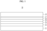
- a quantum dot device 10 includes a first electrode 11 and a second electrode 12 each having a surface facing the other; a quantum dot layer 13 between the first electrode 11 and the second electrode 12; a hole transport layer 14 and a hole injection layer 15 between the first electrode 11 and the quantum dot layer 13; and an electron transport layer 16 and an electron injection layer 17 between the second electrode 12 and the quantum dot layer 13.
- the substrate (not shown) may be disposed under the first electrode 11 or may be disposed on the second electrode 12.
- the substrate may be, for example, made of an inorganic material such as glass; an organic material such as polycarbonate, polymethylmethacrylate, polyethylene terephthalate, polyethylene naphthalate, polyamide, polyethersulfone, or a combination thereof; or a silicon wafer.
- the substrate may be omitted.
- first electrode 11 and the second electrode 12 is an anode and the other is a cathode.
- first electrode 11 may be an anode and the second electrode 12 may be a cathode.
- first electrode 11 may be a cathode and the second electrode 12 may be an anode.
- the anode may include a conductor having a high work function, for example, a metal, a conductive metal oxide, or a combination thereof.
- the anode may include, for example, a metal such as nickel, platinum, vanadium, chromium, copper, zinc, or gold, or an alloy thereof; a conductive metal oxide such as zinc oxide, indium oxide, tin oxide, indium tin oxide (ITO), indium zinc oxide (IZO), or a fluorine-doped tin oxide; or a combination of metal and oxide such as ZnO and Al or SnO 2 and Sb, but is not limited thereto.
- the cathode may include a conductor having a lower work function than the anode, and may include, for example, a metal, a conductive metal oxide, and/or a conductive polymer.
- the cathode may include, for example, a metal such as aluminum, magnesium, calcium, sodium, potassium, titanium, indium, yttrium, lithium, gadolinium silver, tin, lead, cesium, barium, and the like, or an alloy thereof; a multi-layer structure such as LiF/Al, Li 2 O/Al, Liq/Al, LiF/Ca, and BaF 2 /Ca, but is not limited thereto.
- a work function of the anode may be higher than a work function of the cathode, for example the work function of the anode may be, for example, about 4.5 eV to about 5.0 eV and the work function of the cathode may be about 4.0 eV to about 4.7 eV.
- the work function of the anode may be, for example, about 4.6 eV to about 4.9 eV or about 4.6 eV to about 4.8 eV
- the work function of the cathode may be, for example, about 4.0 eV to about 4.6 eV or about 4.3 eV to about 4.6 eV.
- the quantum dot may have, for example, an average particle diameter (an average largest particle length for a non-spherical shape) of for example about 1 nm to about 100 nm, about 1 nm to about 80 nm, about 1 nm to about 50 nm, or about 1 nm to 20 nm.
- an average particle diameter an average largest particle length for a non-spherical shape
- Energy bandgaps of quantum dots may be controlled according to sizes and compositions of the quantum dots, and thus, the light emitting wavelength may be controlled.
- the quantum dots may have narrow energy bandgaps and thus configured to emit light in a relatively long wavelength region while as the sizes of the quantum dots decrease, the quantum dots may have wide energy bandgap and thus configured to emit light in a relatively short wavelength region.
- the quantum dot may be configured to emit light in a predetermined wavelength region of a visible ray region according to its size and/or composition.
- the quantum dot may be configured to emit blue light, red light, or green light
- the blue light may have for example a peak emission wavelength ( ⁇ max ) in about 430 nm to about 480 nm
- the red light may have for example a peak emission wavelength ( ⁇ max ) in about 600 nm to about 650 nm
- the green light may have for example a peak emission wavelength ( ⁇ max ) in about 510 nm to about 560 nm.
- an average particle size of the quantum dot configured to emit blue light may be, for example, less than or equal to about 4.5 nm, and for example, less than or equal to about 4.3 nm, less than or equal to about 4.2 nm, less than or equal to about 4.1 nm, or less than or equal to about 4.0 nm.
- the average particle size of the quantum dot may be about 2.0 nm to about 4.5 nm, for example, about 2.0 nm to about 4.3 nm, about 2.0 nm to about 4.2 nm, about 2.0 nm to about 4.1 nm, or about 2.0 nm to about 4.0 nm.
- the quantum dot may have a relatively narrow full width at half maximum (FWHM).
- FWHM is a width of a wavelength corresponding to a half of a peak absorption point and as the FWHM is narrower, light in a narrower wavelength region may be configured to emit and higher color purity may be obtained.
- the quantum dot may have for example a FWHM of less than or equal to about 50 nm, less than or equal to about 49 nm, less than or equal to about 48 nm, less than or equal to about 47 nm, less than or equal to about 46 nm, less than or equal to about 45 nm, less than or equal to about 44 nm, less than or equal to about 43 nm, less than or equal to about 42 nm, less than or equal to about 41 nm, less than or equal to about 40 nm, less than or equal to about 39 nm, less than or equal to about 38 nm, less than or equal to about 37 nm, less than or equal to about 36 nm, less than or equal to about 35 nm, less than or equal to about 34 nm, less than or equal to about 33 nm, less than or equal to about 32 nm, less than or equal to about 31 nm, less than or equal to about 30 nm, less than or equal to about 29 n
- FWHM of about 2 nm to about 49 nm, about 2 nm to about 48 nm, about 2 nm to about 47 nm, about 2 nm to about 46 nm, about 2 nm to about 45 nm, about 2 nm to about 44 nm, about 2 nm to about 43 nm, about 2 nm to about 42 nm, about 2 nm to about 41 nm, about 2 nm to about 40 nm, about 2 nm to about 39 nm, about 2 nm to about 38 nm, about 2 nm to about 37 nm, about 2 nm to about 36 nm, about 2 nm to about 35 nm, about 2 nm to about 34 nm, about 2 nm to about 33 nm, about 2 nm to about 32 nm, about 2 nm to about 31 nm, about 2 nm to about 30 nm, about 2
- the Group II-VI semiconductor compound may be for example selected from a binary element compound such as CdSe, CdTe, ZnS, ZnSe, ZnTe, ZnO, HgS, HgSe, HgTe, MgSe, MgS, or a mixture thereof; a ternary element compound such as CdSeS, CdSeTe, CdSTe, ZnSeS, ZnSeTe, ZnSTe, HgSeS, HgSeTe, HgSTe, CdZnS, CdZnSe, CdZnTe, CdHgS, CdHgSe, CdHgTe, HgZnS, HgZnSe, HgZnTe, MgZnSe, MgZnS, or a mixture thereof; and a quaternary element compound such as HgZnTeS, CdZnSeS, CdZnSeTe
- the Group III-V semiconductor compound may be for example selected from a binary element compound such as GaN, GaP, GaAs, GaSb, AIN, AlP, AlAs, AlSb, InN, InP, InAs, InSb, or a mixture thereof; a ternary element compound such as GaNP, GaNAs, GaNSb, GaPAs, GaPSb, AINP, AlNAs, AlNSb, AlPAs, AlPSb, InNP, InNAs, InNSb, InPAs, InPSb, or a mixture thereof; and a quaternary element compound such as GaAlNP, GaAINAs, GaAINSb, GaAlPAs, GaAlPSb, GaInNP, GaInNAs, GaInNSb, GaInPAs, GaInPSb, InAlNP, InAINAs, InAINSb, InAlPAs, InAlPSb, or a mixture thereof, but is not limited thereto.
- a binary element compound such as GaN
- the Group IV-VI semiconductor compound may be for example selected from a binary element compound such as SnS, SnSe, SnTe, PbS, PbSe, PbTe, or a mixture thereof; a ternary element compound such as SnSeS, SnSeTe, SnSTe, PbSeS, PbSeTe, PbSTe, SnPbS, SnPbSe, SnPbTe, or a mixture thereof; and a quaternary element compound such as SnPbSSe, SnPbSeTe, SnPbSTe, or a mixture thereof, but is not limited thereto.
- the quantum dot may include the singular element semiconductor, the binary semiconductor compound, the ternary semiconductor compound, or the quaternary semiconductor compound in a substantially uniform concentration or partially different concentration distributions.
- the quantum dot may include a cadmium (Cd)-free quantum dot.
- the cadmium-free quantum dot is a quantum dot that does not include cadmium (Cd).
- Cadmium (Cd) may cause severe environment/health problems and is a restricted element by Restriction of Hazardous Substances Directive (RoHS) in a plurality of countries, and thus the non-cadmium-based quantum dot may be effectively used.
- RoHS Hazardous Substances Directive
- the quantum dot may be a semiconductor compound including indium (In) and at least one of zinc (Zn) and phosphorus (P).
- the quantum dot may be an In-P semiconductor compound and/or an In-Zn-P semiconductor compound.
- a mole ratio of zinc (Zn) to indium (In) may be greater than or equal to about 25.
- the semiconductor compound may have a peak emission wavelength ( ⁇ max ) in a wavelength region of less than about 700 nm, for example about 600 nm to about 650 nm, and may be configured to emit red light.
- the quantum dot having a core-shell structure may for example include a core including a first semiconductor compound including zinc (Zn) and at least one of tellurium (Te) and selenium (Se) and a shell including a second semiconductor compound disposed on at least a portion of the core and having a different composition from that of the core.
- the first semiconductor compound may be a Zn-Te-Se-based semiconductor compound including zinc (Zn), tellurium (Te), and selenium (Se), for example, a Zn-Se-based semiconductor compound including a small amount of tellurium (Te), for example, a semiconductor compound represented by ZnTe x Se 1-x , where x is greater than about 0 and less than or equal to 0.05.
- a mole ratio of tellurium (Te) to selenium (Se) may be less than or equal to about 0.05, less than or equal to about 0.049, less than or equal to about 0.048, less than or equal to about 0.047, less than or equal to about 0.045, less than or equal to about 0.044, less than or equal to about 0.043, less than or equal to about 0.042, less than or equal to about 0.041, less than or equal to about 0.04, less than or equal to about 0.039, less than or equal to about 0.035, less than or equal to about 0.03, less than or equal to about 0.029, less than or equal to about 0.025, less than or equal to about 0.024, less than or equal to about 0.023, less than or equal to about 0.022, less than or equal to about 0.021, less than or equal to about 0.02, less than or equal to about 0.019, less than or equal to about 0.018, less than or equal to about
- a mole ratio of tellurium (Te) to zinc (Zn) may be less than or equal to about 0.02, less than or equal to about 0.019, less than or equal to about 0.018, less than or equal to about 0.017, less than or equal to about 0.016, less than or equal to about 0.015, less than or equal to about 0.014, less than or equal to about 0.013, less than or equal to about 0.012, less than or equal to about 0.011, or less than or equal to about 0.010.
- a quantum dot having a core-shell structure may include a core including a third semiconductor compound including indium (In) and at least one of zinc (Zn) and phosphorus (P) and a shell disposed on at least a portion of the core and including a fourth semiconductor compound having a composition different from the core.
- a mole ratio of zinc (Zn) to indium (In) may be greater than or equal to about 25.
- the mole ratio of zinc (Zn) to indium (In) may be greater than or equal to about 28, greater than or equal to about 29, or greater than or equal to about 30.
- the quantum dot layer 13 may have a thickness of, for example, about 5 nm to about 200 nm, within the range, for example, about 10 nm to about 150 nm, for example about 10 nm to about 100 nm, for example about 10 nm to about 50 nm.
- the quantum dot layer 13 may have a relatively shallow LUMO energy level, for example, less than or equal to about 3.7 eV, within the range, for example, less than or equal to about 3.6 eV, for example, less than or equal to about 3.5 eV, for example, less than or equal to about 3.4 eV, for example less than or equal to about 3.3 eV, for example, less than or equal to about 3.2 eV, for example, less than or equal to about 3.0 eV.
- a relatively shallow LUMO energy level for example, less than or equal to about 3.7 eV, within the range, for example, less than or equal to about 3.6 eV, for example, less than or equal to about 3.5 eV, for example, less than or equal to about 3.4 eV, for example less than or equal to about 3.3 eV, for example, less than or equal to about 3.2 eV, for example, less than or equal to about 3.0 eV.
- the hole transport layer 14 and the hole injection layer 15 are disposed between the first electrode 11 and the quantum dot layer 13.
- the hole transport layer 14 is disposed close to the quantum dot layer 13 between the first electrode 11 and the quantum dot layer 13, and the hole injection layer 15 is disposed close to the first electrode 11 between the first electrode 11 and the quantum dot layer 13.
- the hole injection layer 15 may facilitate injection of holes from the first electrode 11, and the hole transport layer 15 may effectively transfer the injected holes to the quantum dot layer 13.
- the hole transport layer 14 and the hole injection layer 15 may have one or two or more layers, respectively, and may include an electron blocking layer in a broad sense.
- the hole transport layer 14 and the hole injection layer 15 may each have a HOMO energy level between the work function of the first electrode 11 and the HOMO energy level of the quantum dot layer 13.
- the work function of the first electrode 11, the HOMO energy level of the hole injection layer 15, the HOMO energy level of the hole transport layer 14, and the HOMO energy level of the quantum dot layer 13 may gradually become deeper, and may be, for example, stepped.
- the hole transport layer 14 may have a relatively deep HOMO energy level so as to match the HOMO energy level of the quantum dot layer 13. Accordingly, mobility of holes transferred from the hole transport layer 14 to the quantum dot layer 13 may be improved.
- the HOMO energy level of the hole transport layer 14 may be, for example, greater than or equal to about 5.0 eV, within the range, for example, greater than or equal to about 5.2 eV, within the range, for example, greater than or equal to about 5.4 eV, within the range, for example, greater than or equal to about 5.6 eV, within the range, for example, greater than or equal to about 5.8 eV.
- One or both of the hole transport layer 14 and the hole injection layer 15 may be omitted.
- the electron transport layer 16 and the electron injection layer 17 are disposed between the second electrode 12 and the quantum dot layer 13.
- the electron transport layer 16 is disposed close to the quantum dot layer 13 between the second electrode 12 and the quantum dot layer 13, and the electron injection layer 17 is disposed close to the second electrode 12 between the second electrode 12 and the quantum dot layer 13.
- the electron injection layer 17 may facilitate injection of electrons from the second electrode 12, and the electron transport layer 16 may effectively transfer the injected electrons to the quantum dot layer 13.
- the electron transport layer 16 and the electron injection layer 17 may have one or two or more layers, respectively, and may include a hole blocking layer in a broad sense.
- the electron injection layer 17 may be in contact with the second electrode 12.
- the first inorganic nanoparticles may be two-dimensional or three-dimensional nanoparticles with an average particle diameter of less than or equal to about 10 nm, within the range, less than or equal to about 8 nm, less than or equal to about 7 nm, less than or equal to about 5 nm, less than or equal to about 4 nm, or less than or equal to about 3.5 nm, or within the range, about 1 nm to about 10 nm, about 1 nm to about 9 nm, about 1 nm to about 8 nm, about 1 nm to about 7 nm, about 1 nm to about 5 nm, about 1 nm to about 4 nm, or about 1 nm to about 3.5 nm.
- the first inorganic nanoparticles may be a metal oxide nanoparticle including at least one metal of zinc (Zn), magnesium (Mg), cobalt (Co), nickel (Ni), gallium (Ga), aluminum (Al), calcium (Ca), zirconium (Zr), tungsten (W), lithium (Li), titanium (Ti), tantalum (Ta), tin (Sn), hafnium (Hf), or barium (Ba).
- the electron transport layer 16 may include first inorganic nanoparticles and/or aggregates thereof.
- the organic material may be derived from, for example, acetate; carbonyl; carboxylate; acetyl acetonate; an organic amine, or a combination thereof, but is not limited thereto.
- the organic amine may include, for example, a substituted or unsubstituted C1 to C10 alkyl group, a substituted or unsubstituted C6 to C20 aryl group, or a combination thereof, and may include, for example, trimethylamine, triethylamine, tripropylamine, tributylamine, or a combination thereof, but is not limited thereto.
- the organic material in the electron transport layer 16 may be disposed on the surface of the first inorganic nanoparticles and/or between adjacent first inorganic nanoparticles to prevent or minimize aggregation of the first inorganic nanoparticles. Accordingly, it is possible to improve dispersibility of the first inorganic nanoparticles by effectively preventing aggregation of the first inorganic nanoparticles in the dispersion for the electron transport layer including the first inorganic nanoparticles.
- the organic material in the electron transport layer 16 may be in an amount of about 20 wt% to about 70 wt%, about 23 wt% to about 70 wt%, about 25 wt% to about 70 wt%, about 26 wt% to about 70 wt%, about 27 wt% to about 70 wt%, about 28 wt% to about 70 wt%, about 30 wt% to about 70 wt%, about 32 wt% to about 70 wt%, about 35 wt% to about 70 wt%, about 38 wt% to about 70 wt%, about 40 wt% to about 70 wt%, about 42 wt% to about 70 wt%, about 45 wt% to about 70 wt%, about 20 wt% to about 60 wt%, about 23 wt% to about 60 wt%, about 25 wt% to about 60 wt%, about 26 wt% to about 60 wt
- a thickness of the electron transport layer 16 may be greater than about 10 nm and less than or equal to about 80 nm, and within the range, greater than about 10 nm and less than or equal to about 70 nm, greater than about 10 nm and less than or equal to about 60 nm, greater than about 10 nm and less than or equal to about 50 nm, greater than about 10 nm and less than or equal to about 40 nm, or greater than about 10 nm and less than or equal to about 30 nm.
- the electron injection layer 17 may include second inorganic nanoparticles different from the first inorganic nanoparticles.
- the second inorganic nanoparticles may be, for example, oxide nanoparticles, and may be, for example, metal oxide nanoparticles.
- the second inorganic nanoparticle may be selected in consideration of a relationship between the LUMO energy level of the electron transport layer 16 and the electron injection layer 17.
- the second inorganic nanoparticles may be selected so that the LUMO energy level of the electron injection layer 17 including the second inorganic nanoparticles is deeper than the LUMO energy level of the electron transport layer 16 including the aforementioned first inorganic nanoparticles.
- the second inorganic nanoparticles may be two-dimensional or three-dimensional nanoparticles with an average particle diameter of less than or equal to about 10 nm, within the range, less than or equal to about 9 nm, less than or equal to about 8 nm, less than or equal to about 7 nm, less than or equal to about 5 nm, less than or equal to about 4 nm, or less than or equal to about 3.5 nm, or within the range, about 1 nm to about 10 nm, about 1 nm to about 9 nm, about 1 nm to about 8 nm, about 1 nm to about 7 nm, about 1 nm to about 5 nm, about 1 nm to about 4 nm, or about 1 nm to about 3.5 nm.
- the second inorganic nanoparticles may be selected from materials having a higher dispersibility in the dispersion medium than the first inorganic nanoparticles and may be, for example, metal oxide nanoparticle including at least one metal of titanium (Ti), cerium (Ce), tin (Sn), magnesium (Mg), zirconium (Zr), tungsten (W), or aluminum (Al).
- the second inorganic nanoparticles may be for example TiO 2 , CeO 2 , SnO 2 , MgO, ZrO 2 , WO 3 , Al 2 O 3 , or a combination thereof, but are not limited thereto.
- the electron injection layer 17 may further include an organic material.
- the organic material in the electron injection layer 17 may be the same as or different from the organic material in the electron transport layer 16.
- the organic material may be, for example, a material included in the synthesis step of the second inorganic nanoparticles, and may be derived from an organic counteranion of a salt included as a precursor of the second inorganic nanoparticle, such as acetate, carbonyl, carboxylate, acetyl acetonate, organic amine (or organic amine salt), or a combination thereof, but is not limited thereto.
- the amount of the organic material may be reduced by removing at least a portion of the organic material.
- the removing of the organic material may include, for example, centrifugation, precipitation using a solvent and/or dispersion medium, redistribution, and/or washing, but is not limited thereto.
- the electron injection layer 17 may include less organic material than the electron transport layer 16 by including an organic material having a controlled amount.
- a ratio by weight of an amount of the organic material to a total amount of the second inorganic nanoparticles and the organic material in the electron injection layer 17 may be less than a ratio by weight of an amount of the organic material to a total amount of the first inorganic nanoparticles and the organic material in the electron transport layer 16.
- the ratio by weight of the amount of the organic material to a total amount of the second inorganic nanoparticles and the second organic material in the electron injection layer 17 may be about 0.01 times to about 0.9 times, about 0.01 times to about 0.8 times, about 0.01 times to about 0.7 times, or about 0.01 times to about 0.5 times of the ratio by weight of the amount of the organic material to a total amount of the first inorganic nanoparticles and the first organic material in the electron transport layer 16, but is not limited thereto.
- the second inorganic nanoparticles in the electron injection layer 17 may have a higher dispersibility in the dispersion medium than the first inorganic nanoparticles in the electron transport layer 16, and thus even when the organic material in the electron injection layer 17 has a controlled amount, excessive aggregation of the second inorganic nanoparticles may be minimized or, at times, prevented.
- the electron injection layer 17 has a thickness of less than or equal to about 10 nm, even if the electron injection layer has a controlled amount of the organic material, the effect on coatability, morphology, and electrical characteristics of the electron injection layer 17 may become negligible.
- the amount of the organic material in the electron injection layer 17 may be controlled to be less than or equal to about 23 wt%, less than or equal to about 22 wt%, less than or equal to about 20 wt%, less than or equal to about 18 wt%, less than or equal to about 15 wt%, less than or equal to about 12 wt%, less than or equal to about 10 wt%, less than or equal to about 9 wt%, less than or equal to about 8 wt%, less than or equal to about 7 wt%, less than or equal to about 6 wt%, less than or equal to about 5 wt%, less than or equal to about 4 wt%, less than or equal to about 3 wt%, or less than or equal to about 2 wt% based on a total amount of the second inorganic nanoparticles and the organic material.
- the range may be controlled to be about 1 wt% to about 25 wt%, about 1 wt% to about 23 wt%, about 1 wt% to about 22 wt%, about 1 wt% to about 20 wt%, about 1 wt% to about 18 wt%, about 1 wt% to about 15 wt%, about 1 wt% to about 12 wt%, about 1 wt% to about 10 wt%, about 1 wt% to about 9 wt%, about 1 wt% to about 8 wt%, about 1 wt% to about 7 wt%, about 1 wt% to about 6 wt%, about 1 wt% to about 5 wt%, about 1 wt% to about 4 wt%, about 1 wt% to about 3 wt%, or about 1 wt% to about 2 wt%.
- a LUMO energy level of the electron injection layer 17 may be between the work function of the second electrode 12 and the LUMO energy level of the electron transport layer 16.
- a difference between the work function of the second electrode 12 and the LUMO energy level of the electron injection layer 17 may be less than about 0.5 eV, about 0.001 eV to about 0.5 eV, about 0.001 eV to about 0.4 eV, or about 0.001 eV to about 0.3 eV.
- a difference between the LUMO energy level of the electron injection layer 17 and the LUMO energy level of the electron transport layer 16 may be less than about 0.5 eV, about 0.001 eV to about 0.5 eV, about 0.001 eV to about 0.4 eV, or about 0.001 eV to about 0.3 eV. Accordingly, electrons from the second electrode 12 into the electron injection layer 17 may be easily injected to lower a driving voltage of the quantum dot device 10, and electrons from the electron injection layer 17 to the electron transport layer 16 may be effectively transferred to increase efficiency.
- the LUMO energy level of the electron injection layer 17 may be, about 3.4 eV to about 4.8 eV, about 3.4 eV to about 4.6 eV, about 3.4 eV to about 4.5 eV, about 3.6 eV to about 4.8 eV, about 3.6 eV to about 4.6 eV, about 3.6 eV to about 4.5 eV, about 3.6 eV to about 4.3 eV, about 3.9 eV to about 4.8 eV, about 3.9 eV to about 4.6 eV, about 3.9 eV to about 4.5 eV, or about 3.9 eV to about 4.3 eV within the range satisfying the aforementioned energy level.
- the electron injection layer 17 may have a thickness that is less than the thickness of the electron transport layer 16.
- a thickness of the electron injection layer 17 may be about 0.01 times to about 0.8 times, about 0.01 times to about 0.7 times, about 0.01 times to about 0.5 times, about 0.1 times to about 0.8 times, about 0.1 times to about 0.7 times, or about 0.1 times to about 0.5 times of the thickness of the electron transport layer 16.
- the thickness of the electron injection layer 17 may be, for example, less than or equal to about 10 nm, less than or equal to about 7 nm, or less than or equal to about 5 nm. Within the range, the thickness of the electron injection layer 17 may be about 1 nm to about 10 nm, about 1 nm to about 8 nm, about 1 nm to about 7 nm, or about 1 nm to about 5 nm.
- the quantum dot device 10 includes an electron injection layer 17 including an organic material of a controlled amount between the second electrode 12 and the electron transport layer 16, and thereby the electron injection may be effectively facilitated, and the injected electrons may be effectively transferred to the quantum dot layer 13 through the electron transport layer 16. Therefore, it is possible to effectively lower a driving voltage of the quantum dot device 10, thereby improving luminance and life-span.
- the luminance characteristics of the quantum dot device 10 may be improved compared with the quantum dot device that does not include the aforementioned electron injection layer 17, by about 1.05 times to about 3 times, and within the range, about 1.1 times to about 3 times, or about 1.1 times to about 2.5 times.
- the life-span characteristics (T95 or T80) of the quantum dot device 10 may be improved compared with the quantum dot device that does not include the aforementioned electron injection layer 17, by about 1.5 times to about 20 times, and within the range, about 2 times to about 18 times, or about 3 times to about 15 times.
- the quantum dot layer 13, the hole transport layer 14, the hole injection layer 15, the electron transport layer 16, and/or the electron injection layer 17 may be formed by a solution process, such as spin coating, slit coating, inkjet printing, nozzle printing, spraying, and/or doctor blade coating, but is not limited thereto.
- the method of manufacturing a quantum dot device 10 may optionally include drying after the solution process and/or heat-treating may be further performed, and the heat-treating may be, for example, performed at about 50 °C to about 300 °C for about 1 minute to about 10 hours, but is not limited thereto.
- the forming of the electron transport layer 16 may include coating first inorganic nanoparticle dispersion including the first inorganic nanoparticles, and optionally drying and/or heat-treating.
- the first inorganic nanoparticles may be obtained by a sol-gel synthesis method using a metal salt, but is not limited thereto.
- the dispersion medium may be water; alcohols such as methanol, ethanol, propanol, or butanol; or a combination thereof, but is not limited thereto.
- the forming the electron transport layer 16 may include centrifugation and/or washing.
- the forming of the electron injection layer 17 may include coating second inorganic nanoparticle dispersion including second inorganic nanoparticles, and optionally drying and/or heat-treating.
- the second inorganic nanoparticles may be obtained by a sol-gel synthesis method using a metal salt, but is not limited thereto.
- the dispersion medium may be water; alcohols such as methanol, ethanol, propanol, or butanol; or a combination thereof, but is not limited thereto.
- the forming of the electron injection layer 17 may further include removing at least some of the excess organic material from the dispersion in order to control the amount of the organic material as described above.
- the forming of the electron injection layer 17 may include preparing a first dispersion including second inorganic nanoparticles and a first amount of organic material, that is, having an excess amount of organic material, followed by removing at least a portion of the organic material from the first dispersion to prepare a second dispersion including an organic material having a second amount of organic material that is less than the first amount, and coating the second dispersion on the electron transport layer 16.
- the removing of at least a portion of the organic material from the first dispersion may include further performing centrifugation one or more times (e.g., 1 to 10 times, 2 to 10 times, or 3 to 8 times), or further performing precipitation, redispersion, and/or washing one or more times (e.g., 1 to 10 times, 2 to 10 times, or 3 to 8 times) using a polar dispersion medium such as water; alcohols such as methanol, ethanol, propanol, and butanol; a combination of at least one alcohol and water, or a combination of at least one alcohol, and/or a non-polar dispersion medium such as hexane, cyclohexane, benzene, toluene, chloroform, diethyl ether, acetone, etc., or a combination thereof, but is not limited thereto.
- a polar dispersion medium such as water; alcohols such as methanol, ethanol, propanol, and butano
- the amount (second amount) of the organic material in the second dispersion may be less than or equal to about 80 wt%, less than or equal to about 70 wt%, less than or equal to about 50 wt%, less than or equal to about 40 wt%, less than or equal to about 30 wt%, or less than or equal to about 20 wt%, within the range, about 3 wt% to about 80 wt%, about 3 wt% to about 70 wt%, about 3 wt% to about 50 wt%, about 3 wt% to about 40 wt%, about 3 wt% to about 30 wt%, or about 3 wt% to about 20 wt% of the amount (first amount) of the organic material in the first dispersion.
- the amount (the second amount) of organic material in the second dispersion may be controlled to be less than or equal to about 25 wt% based on a total amount of the second inorganic nanoparticles and the organic material (excluding the dispersion medium).
- the method may further include diluting the second dispersion before the coating of the second dispersion.
- the diluting of the second dispersion may further include, for example, further supplying a polar dispersion medium selected from water, at least one alcohol, or a combination thereof to the second dispersion.
- the step of dilution with the polar dispersion medium may including the addition of about 2 times to about 10 times, about 2 times to about 7 times, or about 2 times to about 5 times of the total volume of the second dispersion.
- the aforementioned quantum dot device may be applied to various electronic devices requiring light emission, and may be applied to various electronic devices, for example, a display device such as a TV, a monitor, a computer, and a mobile device, or a lighting device such as a light source.
- a display device such as a TV, a monitor, a computer, and a mobile device
- a lighting device such as a light source.
- TOP trioctylphosphine
- the reactor is cooled down to ambient temperature and ethanol is added to the flask, and the resulting nanocrystals are separated by centrifugation and dispersed in toluene to obtain ZnTeSe core/ZnSeS shell quantum dot dispersion in toluene.
- indium acetate and palmitic acid are added, and the flask is heated at 120 °C under vacuum.
- the indium and palmitic acid are added as a mole ratio of 1:3.
- nitrogen gas is added to the reaction flask, and the flask is heated to 280 °C.
- a mixed solution of tris(trimethylsilyl)phosphine (TMS 3 P) and trioctylphosphine is rapidly injected into the reaction flask, and the reaction mixture is maintained at 280 °C for 20 minutes.
- TMS 3 P is used in an amount of 0.5 mols of TMS 3 P per 1.0 mole of indium.
- the reaction flask is cooled to room temperature and acetone is added to the flask, and the resulting precipitate is separated by centrifugation and dispersed in toluene to prepare InP core quantum dot dispersion in toluene.
- the InP core quantum dot has an average particle diameter of about 3 nanometers (nm).
- TOP trioctylphosphine
- S sulfur
- TOP trioctylphosphine
- reaction flask including trioctylamine, zinc acetate and oleic acid are added, and the reaction flask is heated at 120 °C under vacuum for 10 minutes. Nitrogen gas is added to the reaction flask, the flask is heated to 180 °C, and the InP core quantum dot dispersion is added to the reaction flask.
- the reaction flask is heated to 280 °C, a portion of the Se/TOP is injected into the flask, and the mixture is allowed to react at 280 °C.
- the reaction flask is then heated to 320 °C, the remainder of Se/TOP is injected into the flask, and the reaction mixture allowed to react for predetermined time to form a ZnSe shell on the InP core.
- the S/TOP stock solution is added to the reaction mixture, and the mixture is allowed to react for predetermined time to form a ZnS shell on the ZnSe shell to obtain an InP core/ZnSe shell/ZnS shell quantum dot.
- the ZnSe shell is formed for total reaction time of 60 minutes, and a total amount of Se is about 20 moles based on 1 mole of indium, and the ZnS shell is also formed for total reaction time of 60 minutes, and a total amount of S is about 10 moles based on 1 mole of indium.
- the obtained Zn 0.85 Mg 0.15 O nanoparticles and the ethyl acetate formed in-situ are separated by centrifugation and dispersed in ethanol to obtain a Zn 0.85 Mg 0.15 O nanoparticle dispersion.
- the Zn 0.85 Mg 0.15 O nanoparticles have an average particle diameter of about 3.0 nm.
- the average particle diameter of the Zn 0.85 Mg 0.15 O nanoparticles is measured by using an UT F30 Tecnai electron microscope.
- the Zn 0.85 Mg 0.15 O nanoparticle (ethyl acetate) dispersion is additionally washed with ethanol and redispersed to further reduce an amount of an organic material, i.e., the ethyl acetate, the Zn 0.85 Mg 0.15 O nanoparticles become severely aggregated, and exhibit severe deteriorating dispersibility.
- Titanium oxide (TiO 2 ) nanoparticles (anatase, PlasmaChem) are dispersed in water at a concentration of 20 weight percent (wt%) to prepare a titanium oxide nanoparticle dispersion (first dispersion).
- the titanium oxide nanoparticle dispersion (first dispersion) is centrifuged, and the separated nanoparticles washed repeatedly, at least twice (e.g., 2 to 3 times) with butanol, acetone, and hexane, and redispersed to remove an excessive amount of the organic material and obtain a final precipitate.
- the final precipitate is dispersed in ethanol to obtain titanium oxide nanoparticle dispersion at a concentration of 2 wt% (second dispersion).
- a distribution of particle diameters of the titanium oxide nanoparticles are within about 8 nm or less.
- the particle diameter of the titanium oxide nanoparticles is measured by using a UT F30 Tecnai electron microscope.
- tin oxide nanoparticle dispersion In the tin oxide nanoparticle dispersion (second dispersion), a distribution of particle diameters of tin oxide nanoparticles are within about 8 nm or less. A particle diameter distribution of the tin oxide nanoparticles is measured by using a UT F30 Tecnai electron microscope. Additional ethanol is added to the second dispersion (about three times by volume of the tin oxide nanoparticle dispersion (second dispersion) to obtain tin oxide nanoparticle dispersion at a concentration of 0.5 wt%.
- Tin oxide nanoparticle dispersion is obtained according to the same method as Synthesis Example 5 except that an excessive amount of an organic material is not removed from the tin oxide nanoparticle dispersion (first dispersion).
- An electron-only device is manufactured according to the same method as Example A except that the titanium oxide nanoparticle dispersion prepared according to Comparative Synthesis Example 1 instead of the titanium oxide nanoparticle dispersion of Synthesis Example 4 is used to form the electron injection layer.
- An electron-only device is manufactured according to the same method as Example B except that the SnO 2 nanoparticle dispersion according to Comparative Synthesis Example 2 instead of the SnO 2 dispersion of Synthesis Example 5 is used to form the electron injection layer.
- Example 1-1 Blue Quantum Dot Device
- a glass substrate deposited with ITO (a work function: 4.8 eV) is surface-treated with UV-ozone for 15 minutes.
- a PEDOT:PSS solution (H.C. Starks) is spin-coated on the ITO, and then heat-treated under an air atmosphere at 150 °C for 10 minutes, and heat-treated again under a N 2 atmosphere at 150 °C for 30 minutes to form a 25 nm-thick lower hole transport layer (HOMO: 5.35 eV, LUMO: 3.0 eV).
- a poly[(9,9-dioctylfluoren-2,7-diyl-co-(4,4'-(N-4-butylphenyl)diphenylamine] solution (TFB, Sumitomo Corp.) is spin-coated on the lower hole transport layer and then heat-treated at 150 °C for 30 minutes to form a 25 nm-thick upper hole transport layer (HOMO: 5.6 eV, LUMO: 2.69 eV).
- a quantum dot device is manufactured according to the same method as Example 1-1 except that a 3 nm-thick electron injection layer is formed.
- a quantum dot device is manufactured according to the same method as Example 1-1 except that the InP core/ZnSe shell/ZnS shell quantum dot dispersion (a peak emission wavelength: 629 nm to 630 nm) according to Synthesis Example 2 instead of the ZnTeSe/ZnSeS core shell quantum dot dispersion according to Synthesis Example 1 is used to form a quantum dot layer (HOMO: 5.55 eV, LUMO: 3.6 eV).
- a quantum dot device is manufactured according to the same method as Example 2 except that the titanium oxide nanoparticle dispersion according to Synthesis Example 4 instead of the Zn 0.85 Mg 0.15 O nanoparticle dispersion of Synthesis Example 3 is used to form the electron transport layer, and the Zn 0.85 Mg 0.15 O nanoparticle dispersion according to Synthesis Example 3 instead of the titanium oxide nanoparticle dispersion of Synthesis Example 4 is used to form the electron injection layer.
- a quantum dot device is manufactured according to the same method as Example 3 except that the electron injection layer is not formed on the electron transport layer.
- the current-voltage-luminescence characteristics of the quantum dot devices according to Examples and Comparative examples are evaluated.
- the current-voltage-luminescence characteristics are evaluated by using a Keithley SMU2635B current source and a Minolta CS-2000A spectroradiometer.
- Driving voltages thereof are evaluated by using a voltage (a turn-on voltage) for 5 mA current driving.
- the quantum dot devices according to Examples 1, 2 and 3 simultaneously exhibit a low driving voltage, improved luminescence characteristics, and high life-span characteristics, compared with the quantum dot devices according to the Comparative Examples.
Landscapes
- Chemical & Material Sciences (AREA)
- Physics & Mathematics (AREA)
- Optics & Photonics (AREA)
- Engineering & Computer Science (AREA)
- Materials Engineering (AREA)
- Inorganic Chemistry (AREA)
- Organic Chemistry (AREA)
- Crystallography & Structural Chemistry (AREA)
- Nanotechnology (AREA)
- Luminescent Compositions (AREA)
- Electroluminescent Light Sources (AREA)
Claims (14)
- Dispositif à points quantiques (10), comprenant :une première électrode (11) et une seconde électrode (12) comportant chacune une surface opposée à l'autre ; etune couche de points quantiques (13) entre la première électrode et la seconde électrode, et comprenant en outre :une couche de transport d'électrons (16) entre la couche de points quantiques et la seconde électrode, la couche de transport d'électrons comprenant des premières nanoparticules inorganiques et un premier matériau organique ; etune couche d'injection d'électrons (17) entre la couche de transport d'électrons et la seconde électrode, caractérisé en ce que la couche d'injection d'électrons comprend des secondes nanoparticules inorganiques et un second matériau organique,dans lequel un rapport en poids d'une quantité du second matériau organique à une quantité totale des secondes nanoparticules inorganiques et du second matériau organique dans la couche d'injection d'électrons est inférieur à un rapport en poids d'une quantité du premier matériau organique à une quantité totale des premières nanoparticules inorganiques et du premier matériau organique dans la couche de transport d'électrons.
- Dispositif à points quantiques de la revendication 1, dans lequel le rapport en poids de la quantité du second matériau organique à la quantité totale des secondes nanoparticules inorganiques et du second matériau organique dans la couche d'injection d'électrons est de 0,01 fois à 0,8 fois le rapport en poids de la quantité du premier matériau organique à une quantité totale des premières nanoparticules inorganiques et du premier matériau organique dans la couche de transport d'électrons.
- Dispositif à points quantiques de l'une des revendications 1 ou 2, dans lequel une quantité du second matériau organique dans la couche d'injection d'électrons est inférieure ou égale à25 pour cent en poids, sur la base d'une quantité totale des secondes nanoparticules inorganiques et du second matériau organique.
- Dispositif à points quantiques de l'une quelconque des revendications précédentes, dans lequel les premières nanoparticules inorganiques sont des nanoparticules d'oxyde métallique représentées par Zn1-xQxO, où Q est au moins un métal à l'exclusion de Zn, et 0≤x<0,5, et éventuellement dans lequel l'au moins un métal Q comprend Mg, Co, Ni, Ga, Al, Ca, Zr, W, Li, Ti, Ta, Sn, Hf, Si, Ba, ou une combinaison de ceux-ci.
- Dispositif à points quantiques de l'une quelconque des revendications précédentes, dans lequel les secondes nanoparticules inorganiques sont des nanoparticules d'oxyde métallique qui peuvent être dispersées dans l'eau, l'alcool ou une combinaison de ceux-ci.
- Dispositif à points quantiques de l'une quelconque des revendications précédentes, dans lequel les secondes nanoparticules inorganiques sont des nanoparticules d'oxyde métallique comprenant au moins l'un de Ti, Ce, Sn, Mg, Zr, W ou Al.
- Dispositif à points quantiques de l'une quelconque des revendications précédentes, dans lequel les premières nanoparticules inorganiques sont des nanoparticules d'oxyde métallique représentées par Zn1-xQxO, où Q est au moins un métal à l'exclusion de Zn, et 0≤x<0,5, et
les secondes nanoparticules inorganiques sont différentes des premières nanoparticules inorganiques, les secondes nanoparticules inorganiques comprenant au moins l'un de Ti, Ce, Sn, Mg, Zr, W ou Al. - Dispositif à points quantiques de l'une quelconque des revendications précédentes, dans lequel une épaisseur de la couche d'injection d'électrons est inférieure à une épaisseur de la couche de transport d'électrons.
- Dispositif à points quantiques de l'une quelconque des revendications précédentes, dans lequel l'épaisseur de la couche d'injection d'électrons est inférieure ou égale à 10 nanomètres.
- Dispositif à points quantiques de l'une quelconque des revendications précédentes, dans lequel la couche d'injection d'électrons est en contact avec la seconde électrode.
- Dispositif électronique comprenant le dispositif à points quantiques de l'une quelconque des revendications précédentes.
- Procédé de fabrication d'un dispositif à points quantiques, comprenant la formation d'une première électrode (11) ; etla formation d'une couche de points quantiques (13) sur la première électrode,et caractérisé en ce qu'il comprend en outre :la formation d'une couche de transport d'électrons (16) sur la couche de points quantiques, la couche de transport d'électrons comprenant des premières nanoparticules inorganiques,la formation d'une couche d'injection d'électrons (17) sur la couche de transport d'électrons, la couche d'injection d'électrons comprenant des secondes nanoparticules inorganiques, etla formation d'une seconde électrode (12) sur la couche d'injection d'électrons,dans lequel la formation de la couche d'injection d'électrons comprendla préparation d'une première dispersion comprenant les secondes nanoparticules inorganiques et une première quantité d'un matériau organique,l'élimination d'au moins une partie du matériau organique de la première dispersion pour préparer une seconde dispersion comprenant une seconde quantité de matériau organique inférieure à la première quantité de matériau organique, etle dépôt de la seconde dispersion sur la couche de transport d'électrons.
- Procédé de la revendication 12, comprenant en outre la fourniture d'un milieu de dispersion polaire à la seconde dispersion avant le dépôt de la seconde dispersion, le milieu de dispersion polaire étant l'eau, au moins un alcool ou une combinaison de ceux-ci.
- Procédé de l'une des revendications 12 ou 13, dans lequel une quantité du matériau organique (à l'exclusion du milieu de dispersion) dans la seconde dispersion est inférieure ou égale à 25 pour cent en poids, sur la base d'une quantité totale des secondes nanoparticules inorganiques et du matériau organique.
Applications Claiming Priority (2)
| Application Number | Priority Date | Filing Date | Title |
|---|---|---|---|
| KR20200017693 | 2020-02-13 | ||
| KR1020210017710A KR20210103419A (ko) | 2020-02-13 | 2021-02-08 | 양자점 소자, 양자점 소자의 제조 방법과 전자 장치 |
Publications (2)
| Publication Number | Publication Date |
|---|---|
| EP3869578A1 EP3869578A1 (fr) | 2021-08-25 |
| EP3869578B1 true EP3869578B1 (fr) | 2025-04-16 |
Family
ID=74586826
Family Applications (1)
| Application Number | Title | Priority Date | Filing Date |
|---|---|---|---|
| EP21156163.4A Active EP3869578B1 (fr) | 2020-02-13 | 2021-02-10 | Dispositif à points quantiques, son procédé de fabrication et dispositif électronique |
Country Status (3)
| Country | Link |
|---|---|
| US (1) | US12016241B2 (fr) |
| EP (1) | EP3869578B1 (fr) |
| CN (1) | CN113258012B (fr) |
Families Citing this family (2)
| Publication number | Priority date | Publication date | Assignee | Title |
|---|---|---|---|---|
| KR20230083387A (ko) * | 2021-12-02 | 2023-06-12 | 삼성디스플레이 주식회사 | 발광 소자 및 이를 포함한 전자 장치 |
| WO2026013784A1 (fr) * | 2024-07-10 | 2026-01-15 | シャープディスプレイテクノロジー株式会社 | Élément électroluminescent et dispositif d'affichage |
Family Cites Families (27)
| Publication number | Priority date | Publication date | Assignee | Title |
|---|---|---|---|---|
| US20080278072A1 (en) * | 2007-04-30 | 2008-11-13 | Lg Chem, Ltd. | Organic light emitting device and method of producing the same |
| US20090078933A1 (en) * | 2007-09-21 | 2009-03-26 | Lg Electronics Inc. | Organic light emitting device |
| KR101420327B1 (ko) * | 2008-07-24 | 2014-08-14 | 삼성디스플레이 주식회사 | 유기 발광 소자의 제조 방법 및 유기 발광 소자 |
| DE102009024411A1 (de) | 2009-03-24 | 2010-09-30 | Osram Opto Semiconductors Gmbh | Dünnschichtverkapselung für ein optoelektronisches Bauelement, Verfahren zu dessen Herstellung und optoelektronisches Bauelement |
| KR101658691B1 (ko) | 2009-07-07 | 2016-09-21 | 유니버시티 오브 플로리다 리서치 파운데이션, 인크. | 안정적이고 모든 용액에 처리 가능한 양자점 발광 다이오드 |
| KR101728575B1 (ko) * | 2009-10-07 | 2017-04-19 | 큐디 비젼, 인크. | 양자점을 포함하는 소자 |
| GB2480323A (en) * | 2010-05-14 | 2011-11-16 | Cambridge Display Tech Ltd | OLED hole transport layer |
| WO2013019299A2 (fr) * | 2011-05-11 | 2013-02-07 | Qd Vision, Inc. | Procédé de traitement de dispositifs contenant des points quantiques et dispositifs associés |
| WO2012158252A1 (fr) * | 2011-05-16 | 2012-11-22 | Qd Vision, Inc. | Dispositif comprenant des points quantiques et son procédé de fabrication |
| WO2012161179A1 (fr) | 2011-05-26 | 2012-11-29 | 株式会社 村田製作所 | Dispositif électroluminescent |
| US9711748B2 (en) * | 2012-08-29 | 2017-07-18 | Boe Technology Group Co., Ltd. | OLED devices with internal outcoupling |
| WO2014088667A2 (fr) * | 2012-09-14 | 2014-06-12 | Qd Vision, Inc. | Dispositif électroluminescent comprenant une structure en tandem |
| KR101626525B1 (ko) | 2014-09-18 | 2016-06-01 | 홍익대학교 산학협력단 | 합금화된 나노입자 전자 수송층을 포함하는 양자점-발광 소자 및 그 제조방법 |
| CN105322098B (zh) * | 2015-11-03 | 2018-06-19 | Tcl集团股份有限公司 | 一种可提高电荷注入平衡的量子点发光二极管及制备方法 |
| CN106784357B (zh) * | 2017-01-04 | 2019-05-14 | 纳晶科技股份有限公司 | 发光器件、含其的显示装置及照明装置、和太阳能电池 |
| US10516132B2 (en) | 2017-08-24 | 2019-12-24 | Shenzhen China Star Optoelectronics Semiconductor Display Technology Co., Ltd. | Inverted quantum dot light-emitting diode and manufacturing method thereof |
| KR102322292B1 (ko) * | 2017-08-24 | 2021-11-04 | 주식회사 엘지화학 | 유기전자소자 및 이의 제조방법 |
| KR102349593B1 (ko) | 2017-09-26 | 2022-01-10 | 엘지디스플레이 주식회사 | 발광다이오드 및 이를 포함하는 발광장치 |
| KR102375620B1 (ko) * | 2017-10-16 | 2022-03-16 | 엘지디스플레이 주식회사 | 발광다이오드 및 이를 포함하는 발광장치 |
| KR102371410B1 (ko) * | 2017-10-26 | 2022-03-04 | 엘지디스플레이 주식회사 | 발광다이오드 및 이를 포함하는 발광장치 |
| KR102443644B1 (ko) | 2017-11-20 | 2022-09-14 | 삼성전자주식회사 | 양자점 소자와 표시 장치 |
| CN108963087A (zh) * | 2017-11-29 | 2018-12-07 | 广东聚华印刷显示技术有限公司 | 量子点电致发光器件及显示器 |
| KR101980979B1 (ko) | 2017-12-07 | 2019-05-21 | 경희대학교 산학협력단 | 전자 수송층을 포함하는 박막형 발광소자 및 그 제조 방법 |
| KR102736144B1 (ko) * | 2017-12-19 | 2024-11-29 | 삼성전자주식회사 | 전계 발광 소자 및 이를 포함하는 표시 장치 |
| KR102452648B1 (ko) | 2017-12-27 | 2022-10-06 | 삼성전자주식회사 | 전계 발광 소자 및 이를 포함하는 표시 장치 |
| CN110246972B (zh) * | 2018-03-09 | 2025-01-24 | 三星电子株式会社 | 量子点器件和电子装置 |
| KR102611215B1 (ko) * | 2018-03-12 | 2023-12-06 | 삼성전자주식회사 | 전계 발광 소자, 및 표시 장치 |
-
2021
- 2021-02-09 US US17/171,008 patent/US12016241B2/en active Active
- 2021-02-10 CN CN202110183999.8A patent/CN113258012B/zh active Active
- 2021-02-10 EP EP21156163.4A patent/EP3869578B1/fr active Active
Also Published As
| Publication number | Publication date |
|---|---|
| EP3869578A1 (fr) | 2021-08-25 |
| CN113258012A (zh) | 2021-08-13 |
| CN113258012B (zh) | 2025-08-19 |
| US12016241B2 (en) | 2024-06-18 |
| US20210257551A1 (en) | 2021-08-19 |
Similar Documents
| Publication | Publication Date | Title |
|---|---|---|
| US11793011B2 (en) | Quantum dot device and display device | |
| EP3683853B1 (fr) | Dispositif à points quantiques et dispositif électronique | |
| US10446782B1 (en) | Quantum dot device and electronic device | |
| EP3599265B1 (fr) | Dispositif à points quantiques et dispositif d'affichage | |
| EP3809474B1 (fr) | Dispositif électroluminescent à points quantiques et dispositif électronique | |
| KR102217328B1 (ko) | 발광 소자와 이를 포함한 표시 장치 | |
| US10535829B1 (en) | Quantum dot device and display device | |
| US11910629B2 (en) | Light emitting device, method of manufacturing the same, and display device | |
| EP3869578B1 (fr) | Dispositif à points quantiques, son procédé de fabrication et dispositif électronique | |
| US11611054B2 (en) | Quantum dot device and electronic device | |
| KR20210103419A (ko) | 양자점 소자, 양자점 소자의 제조 방법과 전자 장치 | |
| EP4601438A1 (fr) | Dispositif électroluminescent à points quantiques et son procédé de fabrication et dispositif électronique | |
| EP3882999B1 (fr) | Dispositif à points quantiques et dispositif électronique | |
| US12225747B2 (en) | Quantum dot device and electronic device |
Legal Events
| Date | Code | Title | Description |
|---|---|---|---|
| PUAI | Public reference made under article 153(3) epc to a published international application that has entered the european phase |
Free format text: ORIGINAL CODE: 0009012 |
|
| STAA | Information on the status of an ep patent application or granted ep patent |
Free format text: STATUS: THE APPLICATION HAS BEEN PUBLISHED |
|
| AK | Designated contracting states |
Kind code of ref document: A1 Designated state(s): AL AT BE BG CH CY CZ DE DK EE ES FI FR GB GR HR HU IE IS IT LI LT LU LV MC MK MT NL NO PL PT RO RS SE SI SK SM TR |
|
| STAA | Information on the status of an ep patent application or granted ep patent |
Free format text: STATUS: REQUEST FOR EXAMINATION WAS MADE |
|
| 17P | Request for examination filed |
Effective date: 20220224 |
|
| RBV | Designated contracting states (corrected) |
Designated state(s): AL AT BE BG CH CY CZ DE DK EE ES FI FR GB GR HR HU IE IS IT LI LT LU LV MC MK MT NL NO PL PT RO RS SE SI SK SM TR |
|
| P01 | Opt-out of the competence of the unified patent court (upc) registered |
Effective date: 20230520 |
|
| REG | Reference to a national code |
Ref country code: DE Ref legal event code: R079 Free format text: PREVIOUS MAIN CLASS: H01L0051500000 Ipc: H10K0050160000 Ref document number: 602021029100 Country of ref document: DE |
|
| RIC1 | Information provided on ipc code assigned before grant |
Ipc: H10K 50/17 20230101ALI20241017BHEP Ipc: H10K 50/16 20230101AFI20241017BHEP |
|
| GRAP | Despatch of communication of intention to grant a patent |
Free format text: ORIGINAL CODE: EPIDOSNIGR1 |
|
| STAA | Information on the status of an ep patent application or granted ep patent |
Free format text: STATUS: GRANT OF PATENT IS INTENDED |
|
| INTG | Intention to grant announced |
Effective date: 20241128 |
|
| GRAS | Grant fee paid |
Free format text: ORIGINAL CODE: EPIDOSNIGR3 |
|
| GRAA | (expected) grant |
Free format text: ORIGINAL CODE: 0009210 |
|
| STAA | Information on the status of an ep patent application or granted ep patent |
Free format text: STATUS: THE PATENT HAS BEEN GRANTED |
|
| AK | Designated contracting states |
Kind code of ref document: B1 Designated state(s): AL AT BE BG CH CY CZ DE DK EE ES FI FR GB GR HR HU IE IS IT LI LT LU LV MC MK MT NL NO PL PT RO RS SE SI SK SM TR |
|
| REG | Reference to a national code |
Ref country code: GB Ref legal event code: FG4D |
|
| REG | Reference to a national code |
Ref country code: CH Ref legal event code: EP Ref country code: DE Ref legal event code: R096 Ref document number: 602021029100 Country of ref document: DE |
|
| REG | Reference to a national code |
Ref country code: IE Ref legal event code: FG4D |
|
| REG | Reference to a national code |
Ref country code: NL Ref legal event code: MP Effective date: 20250416 |
|
| PG25 | Lapsed in a contracting state [announced via postgrant information from national office to epo] |
Ref country code: NL Free format text: LAPSE BECAUSE OF FAILURE TO SUBMIT A TRANSLATION OF THE DESCRIPTION OR TO PAY THE FEE WITHIN THE PRESCRIBED TIME-LIMIT Effective date: 20250416 |
|
| REG | Reference to a national code |
Ref country code: AT Ref legal event code: MK05 Ref document number: 1786791 Country of ref document: AT Kind code of ref document: T Effective date: 20250416 |
|
| PG25 | Lapsed in a contracting state [announced via postgrant information from national office to epo] |
Ref country code: PT Free format text: LAPSE BECAUSE OF FAILURE TO SUBMIT A TRANSLATION OF THE DESCRIPTION OR TO PAY THE FEE WITHIN THE PRESCRIBED TIME-LIMIT Effective date: 20250818 Ref country code: FI Free format text: LAPSE BECAUSE OF FAILURE TO SUBMIT A TRANSLATION OF THE DESCRIPTION OR TO PAY THE FEE WITHIN THE PRESCRIBED TIME-LIMIT Effective date: 20250416 Ref country code: ES Free format text: LAPSE BECAUSE OF FAILURE TO SUBMIT A TRANSLATION OF THE DESCRIPTION OR TO PAY THE FEE WITHIN THE PRESCRIBED TIME-LIMIT Effective date: 20250416 |
|
| REG | Reference to a national code |
Ref country code: LT Ref legal event code: MG9D |
|
| PG25 | Lapsed in a contracting state [announced via postgrant information from national office to epo] |
Ref country code: GR Free format text: LAPSE BECAUSE OF FAILURE TO SUBMIT A TRANSLATION OF THE DESCRIPTION OR TO PAY THE FEE WITHIN THE PRESCRIBED TIME-LIMIT Effective date: 20250717 Ref country code: NO Free format text: LAPSE BECAUSE OF FAILURE TO SUBMIT A TRANSLATION OF THE DESCRIPTION OR TO PAY THE FEE WITHIN THE PRESCRIBED TIME-LIMIT Effective date: 20250716 |
|
| PG25 | Lapsed in a contracting state [announced via postgrant information from national office to epo] |
Ref country code: PL Free format text: LAPSE BECAUSE OF FAILURE TO SUBMIT A TRANSLATION OF THE DESCRIPTION OR TO PAY THE FEE WITHIN THE PRESCRIBED TIME-LIMIT Effective date: 20250416 |
|
| PG25 | Lapsed in a contracting state [announced via postgrant information from national office to epo] |
Ref country code: BG Free format text: LAPSE BECAUSE OF FAILURE TO SUBMIT A TRANSLATION OF THE DESCRIPTION OR TO PAY THE FEE WITHIN THE PRESCRIBED TIME-LIMIT Effective date: 20250416 |
|
| PG25 | Lapsed in a contracting state [announced via postgrant information from national office to epo] |
Ref country code: HR Free format text: LAPSE BECAUSE OF FAILURE TO SUBMIT A TRANSLATION OF THE DESCRIPTION OR TO PAY THE FEE WITHIN THE PRESCRIBED TIME-LIMIT Effective date: 20250416 |
|
| PG25 | Lapsed in a contracting state [announced via postgrant information from national office to epo] |
Ref country code: AT Free format text: LAPSE BECAUSE OF FAILURE TO SUBMIT A TRANSLATION OF THE DESCRIPTION OR TO PAY THE FEE WITHIN THE PRESCRIBED TIME-LIMIT Effective date: 20250416 |
|
| PG25 | Lapsed in a contracting state [announced via postgrant information from national office to epo] |
Ref country code: RS Free format text: LAPSE BECAUSE OF FAILURE TO SUBMIT A TRANSLATION OF THE DESCRIPTION OR TO PAY THE FEE WITHIN THE PRESCRIBED TIME-LIMIT Effective date: 20250716 |
|
| PG25 | Lapsed in a contracting state [announced via postgrant information from national office to epo] |
Ref country code: IS Free format text: LAPSE BECAUSE OF FAILURE TO SUBMIT A TRANSLATION OF THE DESCRIPTION OR TO PAY THE FEE WITHIN THE PRESCRIBED TIME-LIMIT Effective date: 20250816 |
|
| PG25 | Lapsed in a contracting state [announced via postgrant information from national office to epo] |
Ref country code: LV Free format text: LAPSE BECAUSE OF FAILURE TO SUBMIT A TRANSLATION OF THE DESCRIPTION OR TO PAY THE FEE WITHIN THE PRESCRIBED TIME-LIMIT Effective date: 20250416 |
|
| PG25 | Lapsed in a contracting state [announced via postgrant information from national office to epo] |
Ref country code: SM Free format text: LAPSE BECAUSE OF FAILURE TO SUBMIT A TRANSLATION OF THE DESCRIPTION OR TO PAY THE FEE WITHIN THE PRESCRIBED TIME-LIMIT Effective date: 20250416 Ref country code: DK Free format text: LAPSE BECAUSE OF FAILURE TO SUBMIT A TRANSLATION OF THE DESCRIPTION OR TO PAY THE FEE WITHIN THE PRESCRIBED TIME-LIMIT Effective date: 20250416 |
|
| PG25 | Lapsed in a contracting state [announced via postgrant information from national office to epo] |
Ref country code: CZ Free format text: LAPSE BECAUSE OF FAILURE TO SUBMIT A TRANSLATION OF THE DESCRIPTION OR TO PAY THE FEE WITHIN THE PRESCRIBED TIME-LIMIT Effective date: 20250416 |
|
| PG25 | Lapsed in a contracting state [announced via postgrant information from national office to epo] |
Ref country code: EE Free format text: LAPSE BECAUSE OF FAILURE TO SUBMIT A TRANSLATION OF THE DESCRIPTION OR TO PAY THE FEE WITHIN THE PRESCRIBED TIME-LIMIT Effective date: 20250416 |
|
| PG25 | Lapsed in a contracting state [announced via postgrant information from national office to epo] |
Ref country code: SK Free format text: LAPSE BECAUSE OF FAILURE TO SUBMIT A TRANSLATION OF THE DESCRIPTION OR TO PAY THE FEE WITHIN THE PRESCRIBED TIME-LIMIT Effective date: 20250416 Ref country code: RO Free format text: LAPSE BECAUSE OF FAILURE TO SUBMIT A TRANSLATION OF THE DESCRIPTION OR TO PAY THE FEE WITHIN THE PRESCRIBED TIME-LIMIT Effective date: 20250416 |
|
| PG25 | Lapsed in a contracting state [announced via postgrant information from national office to epo] |
Ref country code: IT Free format text: LAPSE BECAUSE OF FAILURE TO SUBMIT A TRANSLATION OF THE DESCRIPTION OR TO PAY THE FEE WITHIN THE PRESCRIBED TIME-LIMIT Effective date: 20250416 |