EP3869566A1 - Trench gate depletion-type vdmos device and manufacturing method therefor - Google Patents
Trench gate depletion-type vdmos device and manufacturing method therefor Download PDFInfo
- Publication number
- EP3869566A1 EP3869566A1 EP19872401.5A EP19872401A EP3869566A1 EP 3869566 A1 EP3869566 A1 EP 3869566A1 EP 19872401 A EP19872401 A EP 19872401A EP 3869566 A1 EP3869566 A1 EP 3869566A1
- Authority
- EP
- European Patent Office
- Prior art keywords
- conductive type
- region
- trench
- type doped
- doped region
- Prior art date
- Legal status (The legal status is an assumption and is not a legal conclusion. Google has not performed a legal analysis and makes no representation as to the accuracy of the status listed.)
- Pending
Links
Images


Classifications
-
- H—ELECTRICITY
- H10—SEMICONDUCTOR DEVICES; ELECTRIC SOLID-STATE DEVICES NOT OTHERWISE PROVIDED FOR
- H10D—INORGANIC ELECTRIC SEMICONDUCTOR DEVICES
- H10D62/00—Semiconductor bodies, or regions thereof, of devices having potential barriers
- H10D62/10—Shapes, relative sizes or dispositions of the regions of the semiconductor bodies; Shapes of the semiconductor bodies
- H10D62/102—Constructional design considerations for preventing surface leakage or controlling electric field concentration
- H10D62/103—Constructional design considerations for preventing surface leakage or controlling electric field concentration for increasing or controlling the breakdown voltage of reverse-biased devices
- H10D62/105—Constructional design considerations for preventing surface leakage or controlling electric field concentration for increasing or controlling the breakdown voltage of reverse-biased devices by having particular doping profiles, shapes or arrangements of PN junctions; by having supplementary regions, e.g. junction termination extension [JTE]
- H10D62/109—Reduced surface field [RESURF] PN junction structures
- H10D62/111—Multiple RESURF structures, e.g. double RESURF or 3D-RESURF structures
-
- H—ELECTRICITY
- H10—SEMICONDUCTOR DEVICES; ELECTRIC SOLID-STATE DEVICES NOT OTHERWISE PROVIDED FOR
- H10D—INORGANIC ELECTRIC SEMICONDUCTOR DEVICES
- H10D30/00—Field-effect transistors [FET]
- H10D30/01—Manufacture or treatment
- H10D30/021—Manufacture or treatment of FETs having insulated gates [IGFET]
- H10D30/025—Manufacture or treatment of FETs having insulated gates [IGFET] of vertical IGFETs
-
- H—ELECTRICITY
- H10—SEMICONDUCTOR DEVICES; ELECTRIC SOLID-STATE DEVICES NOT OTHERWISE PROVIDED FOR
- H10D—INORGANIC ELECTRIC SEMICONDUCTOR DEVICES
- H10D30/00—Field-effect transistors [FET]
- H10D30/01—Manufacture or treatment
- H10D30/021—Manufacture or treatment of FETs having insulated gates [IGFET]
- H10D30/028—Manufacture or treatment of FETs having insulated gates [IGFET] of double-diffused metal oxide semiconductor [DMOS] FETs
- H10D30/0291—Manufacture or treatment of FETs having insulated gates [IGFET] of double-diffused metal oxide semiconductor [DMOS] FETs of vertical DMOS [VDMOS] FETs
- H10D30/0297—Manufacture or treatment of FETs having insulated gates [IGFET] of double-diffused metal oxide semiconductor [DMOS] FETs of vertical DMOS [VDMOS] FETs using recessing of the gate electrodes, e.g. to form trench gate electrodes
-
- H—ELECTRICITY
- H10—SEMICONDUCTOR DEVICES; ELECTRIC SOLID-STATE DEVICES NOT OTHERWISE PROVIDED FOR
- H10D—INORGANIC ELECTRIC SEMICONDUCTOR DEVICES
- H10D30/00—Field-effect transistors [FET]
- H10D30/60—Insulated-gate field-effect transistors [IGFET]
- H10D30/63—Vertical IGFETs
- H10D30/635—Vertical IGFETs having no inversion channels, e.g. vertical accumulation channel FETs [ACCUFET] or normally-on vertical IGFETs
-
- H—ELECTRICITY
- H10—SEMICONDUCTOR DEVICES; ELECTRIC SOLID-STATE DEVICES NOT OTHERWISE PROVIDED FOR
- H10D—INORGANIC ELECTRIC SEMICONDUCTOR DEVICES
- H10D30/00—Field-effect transistors [FET]
- H10D30/60—Insulated-gate field-effect transistors [IGFET]
- H10D30/64—Double-diffused metal-oxide semiconductor [DMOS] FETs
- H10D30/66—Vertical DMOS [VDMOS] FETs
- H10D30/668—Vertical DMOS [VDMOS] FETs having trench gate electrodes, e.g. UMOS transistors
-
- H—ELECTRICITY
- H10—SEMICONDUCTOR DEVICES; ELECTRIC SOLID-STATE DEVICES NOT OTHERWISE PROVIDED FOR
- H10D—INORGANIC ELECTRIC SEMICONDUCTOR DEVICES
- H10D62/00—Semiconductor bodies, or regions thereof, of devices having potential barriers
- H10D62/10—Shapes, relative sizes or dispositions of the regions of the semiconductor bodies; Shapes of the semiconductor bodies
-
- H—ELECTRICITY
- H10—SEMICONDUCTOR DEVICES; ELECTRIC SOLID-STATE DEVICES NOT OTHERWISE PROVIDED FOR
- H10D—INORGANIC ELECTRIC SEMICONDUCTOR DEVICES
- H10D62/00—Semiconductor bodies, or regions thereof, of devices having potential barriers
- H10D62/10—Shapes, relative sizes or dispositions of the regions of the semiconductor bodies; Shapes of the semiconductor bodies
- H10D62/124—Shapes, relative sizes or dispositions of the regions of semiconductor bodies or of junctions between the regions
-
- H—ELECTRICITY
- H10—SEMICONDUCTOR DEVICES; ELECTRIC SOLID-STATE DEVICES NOT OTHERWISE PROVIDED FOR
- H10D—INORGANIC ELECTRIC SEMICONDUCTOR DEVICES
- H10D64/00—Electrodes of devices having potential barriers
- H10D64/20—Electrodes characterised by their shapes, relative sizes or dispositions
- H10D64/27—Electrodes not carrying the current to be rectified, amplified, oscillated or switched, e.g. gates
- H10D64/311—Gate electrodes for field-effect devices
- H10D64/411—Gate electrodes for field-effect devices for FETs
- H10D64/511—Gate electrodes for field-effect devices for FETs for IGFETs
- H10D64/512—Disposition of the gate electrodes, e.g. buried gates
- H10D64/513—Disposition of the gate electrodes, e.g. buried gates within recesses in the substrate, e.g. trench gates, groove gates or buried gates
Definitions
- the invention relates to the field of semiconductor manufacturing, and in particular, to a trench gate depletion mode VDMOS device and a method for manufacturing the trench gate depletion mode VDMOS device.
- a depletion mode VDMOS vertical double diffused metal oxide semiconductor field effect transistor
- a depletion mode VDMOS usually operates during a start-up stage of a circuit. When the circuit has been started and transitioned to its stable operating state, a conductive channel of the depletion mode VDMOS is pinched off to cut off this device, thereby enabling the circuit to operate normally.
- a longitudinal channel of such a trench gate depletion mode VDMOS can be easily depleted and pinched off, and the pinch-off current is stable. Due to these advantages, such a trench gate depletion mode VDMOS has been widely used in medium and small power circuits and systems.
- a large start-up current would pass through the depletion mode VDMOS, which is often higher than the current of the circuit at the stable operating state. Therefore, a key point in design of a depletion mode device is to increase the operating current of the depletion mode device at an ON-state. Low on-resistance has become an important design index for a depletion mode VDMOS, and this is also true for a trench gate depletion mode VDMOS.
- a trench gate depletion mode VDMOS device comprises: a drain region being of a first conductive type; a trench gate including a gate insulating layer on an inner surface of a trench and a gate electrode filled in the trench and surrounded by the gate insulating layer; a channel region located around the gate insulating layer and being of the first conductive type; a well region located on both sides of the trench gate and being of a second conductive type, the first conductive type is a conductive type opposite to the second conductive type; a source region located in the well region and being of the first conductive type; a drift region located between the well region and the drain region and being of the first conductive type; a second conductive type doped region located between the channel region and the drain region; a first conductive type doped region located on both sides of the second conductive type doped region and located between the drift region and the drain region.
- a method for manufacturing a trench gate depletion mode VDMOS device comprises: providing a substrate, the substrate includes a first conductive type doped region and a drift region of a first conductive type on the first conductive type doped region; forming a trench by etching the drift region; doping on the side walls of the trench and forming a channel region in the trench; doping impurities of a second conductive type into an area of the first conductive type doped region around the bottom of the trench, such that a second conductive type doped region is formed within the first conductive type doped region; the first conductive type is an conductive type opposite to the second conductive type; forming a gate insulating layer on the inner surface of the trench; forming a gate electrode by filling the remaining space in the trench; doping impurities of the second conductive type on the surface of the drift region and forming a well region on both sides of the trench; doping impurities of the first conductive type into the well region, such that a source region is formed.
- a spatial relationship term such as “under”, “below”, “on”, “above”, and etc., can be used herein to describe a relationship between one element or feature and another component or feature shown in the figures. It should be understood that, in addition to an orientation shown in a figure, such a spatial relationship term is also intended to include different orientations of a device in use and operation. For example, if a device in a figure is turned over, then an element or feature described as being “under another element” or “below another element” or “beneath another element” would then be oriented to be “above” the other element or feature. Therefore, the exemplary terms “below” and “under” could include the following two orientations: below and above. The device may be otherwise oriented (rotated 90 degrees or other orientations) and the spatial descriptions used herein are interpreted accordingly.
- Embodiments of the invention are described herein with reference to cross-sectional views that are schematic views of idealized embodiments (and intermediate structures) of the present invention. In this way, changes from the illustrated shapes due to, for example, manufacturing techniques and/or tolerances can be expected. Therefore, embodiments of the present invention should not be limited to the specific shapes of the regions shown herein, but include deviations in shape due to, for example, manufacturing. For example, an implanted region illustrated as a rectangle usually has a circular or curved feature at its edge, and/or has an implantation concentration gradient, rather than a binary change from the implanted region to a non-implanted region.
- a buried region formed by implantation may lead to some implantation in the buried region and in regions between surfaces that the implantation passes through. Therefore, the regions shown in the figures are essentially schematic, and the shapes of them are not intended to illustrate the actual shapes of the regions of a device and are not intended to limit the scope of the invention.
- P type and N type impurities in order to distinguish the doping concentrations, simply P+ type is used to represent a P type impurity with a heavy doping concentration, P type is used to represent a P type impurity with a medium doping concentration, P- type is used to represent a P type impurity with a light doping concentration, N+ type is used to represent an N type impurity with a heavy doping concentration, N type is used to represent an N type impurity with a medium doping concentration, and N- type is used to represent an N type impurity with a light doping concentration.
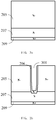
- FIG. 1 is a schematic structure diagram of a trench gate depletion mode VDMOS device in an embodiment.
- the trench gate depletion mode VDMOS device includes a drain region 209, a trench gate (including a gate insulating layer 204 and a gate electrode 201), a channel region 206, a well region 202, a source region 203, a drift region 205, a second conductive type doped region 208 and a first conductive type doped region 207.
- the drain region 209 is a drain region of a first conductive type, which is led out as a drain terminal of the VDMOS.
- the first conductive type is N type and the second conductive type is P type.
- the gate insulating layer 204 is arranged on an inner surface of a trench (which is the trench of the trench gate), and the gate electrode 201 is filled in the trench and is surrounded by the gate insulating layer 204.
- the channel region 206 is located around the gate insulating layer 204 and is a conductive channel of the first conductive type. Since the channel region is the channel of the depletion mode transistor, it is a normally-on channel.
- the well region 202 is located on both sides of the trench gate and is a well region of the second conductive type.
- the well region serves as a substrate of the depletion mode transistor, such that a longitudinal conductive channel is formed.
- the source region 203 is located within the well region 202 and is a source region of the first conductive type.
- the source region serves as an ohmic contact at a source terminal.
- the drift region 205 is located between the well region 202 and the drain region 209 and is a drift region of the first conductive type.
- the second conductive type doped region 208 is located between the channel region 206 and the drain region 209.
- the second conductive type doped region 208 is a P- well, and one end of the P- well is in contact with the channel region 206 and the other end is in contact with the drain region 209.
- the first conductive type doped region 207 is located on both sides of the second conductive type doped region 208, and is located between the drift region 205 and the drain region 209.
- the first conductive type doped region 207 is an N well.
- a PN structure of the second conductive type doped region 208 and the first conductive type doped region 207 is formed at the bottom of the trench.
- a charge balance is achieved between electrons and holes in this region.
- the charge balance region has a lower resistance.
- the trench gate depletion mode VDMOS device also includes a body lead-out region of a second conductive type (i.e., a P+ region adjacent to the source region 203, not indicted in FIG. 1 ) in the well region 202.
- a second conductive type i.e., a P+ region adjacent to the source region 203, not indicted in FIG. 1
- the doping concentration of the second conductive type doped region 208 is less than that of the well region 202
- the doping concentration of the well region 202 is less than that of the body lead-out region.
- the well region 202 is a high-voltage P type well.
- the first conductive type doped region 207 and the second conductive type doped region 208 are a N type well and a P type well with a super junction structure, respectively.
- the bottom of the channel region 206 extends into the second conductive type doped region 208.
- a traditional trench gate depletion mode VDMOS transistor there would be a weak point produced at the bottom of its trench when it is under a withstand voltage in an OFF-state. Specifically, because of a larger curvature at the bottom of the trench, a highest impact ionization rate is generally concentrated on a sharp corner at the bottom of the trench when the device is under a reverse withstand voltage, causing this position to break down easily.
- the channel region 206 at the bottom of the trench is wrapped into the second conductive type doped region 208.
- a reverse depletion layer is formed by the N-P structures of the drift region 205 - the second conductive type doped region 208 and the channel area 206 - the second conductive type doped region 208.
- the trench gate is at a zero potential, and the second conductive type doped region 208 is still at a low potential, the second conductive type doped region 208 is involved in the whole depletion withstand voltage process, and the trench gate is not involved in, thereby effectively avoiding the weak point of the sharp corner at the bottom of the trench, and improving the stability of the withstand voltage.
- the doping concentration of the first conductive type doped region 207 is greater than that of the drift region 205, and the doping concentration of the drain region 209 is greater than that of the first conductive type doped region 207.
- the doping concentration of drift region 205 is lower, which corresponds to a high resistance region being formed between the source and drain.
- the breakdown voltage can be increased, the parasitic capacitance between the source and drain can be reduced, and the frequency characteristics of the device can be advantageously improved.
- the carrier concentration of the N+ type doped drain region at the bottom of it is quite different from that of the N- type drift region.
- the thermal process during the formation of the P type well will lead to a large amount of N+ to be reversely diffused into the drift region and the effective drift region to be greatly reduced in thickness.
- increasing a margin of a N-type epitaxial i.e., the N-type epitaxial serves as a N-type drift region
- a N type well i.e., a first conductive type doped region 207 present under the drift region 205, which corresponds to a carrier concentration buffer region being formed between the drain region 209 (N+) and the drift region 205 (N-).
- the concentration of the drift region 205 became more stable (less N type impurities are diffused into the drift region 205 from below), the reverse withstand voltage can be better utilized, and there is no need to reserve a lager margin for the drift region 205.
- the drift region 205 with a higher resistance can be made thinner, and the on-resistance can be reduced.
- the gate insulating layer 204 may include a conventional dielectric material such as silicon oxide, silicon nitride, and silicon oxynitride having a dielectric constant from about 4 to about 20 (measured in vacuum).
- the gate insulating layer 204 may include a generally higher dielectric constant dielectric material having a dielectric constant from about 20 to at least about 100.
- Such a higher dielectric constant dielectric material can include but is not limited to hafnium oxide, hafnium silicate, titanium oxide, barium strontium titanate (BSTs) and lead zirconate titanate (PZTs).
- the gate electrode 201 is a polysilicon material, and in other embodiments, metal, metal nitride, metal silicide, or a similar compound may also be used as a material of the gate electrode 201.
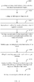
- FIG. 2 is a flow chart of a method for manufacturing a trench gate depletion mode VDMOS device in an embodiment. The method includes the following steps:
- a substrate is provided.
- the substrate includes a first conductive type doped region 207 and a drift region 205.
- firstly the first conductive type doped region 207 of N type is epitaxially formed on the substrate of N+ type (which is used as a drain region 209), and then the drift region 205 of N- type is epitaxially formed on the first conductive type doped region 207.
- the doping concentration of the drain region 209 is higher than that of the first conductive type doped region 207, and the doping concentration of the first conductive type doped region 207 is greater than that of the drift region 205.
- the step of forming the drain region 209 can also be happened in a subsequent step and is carried out by a process familiar to those skilled in the art (e.g., ion injection).
- the drift region 205 may be epitaxially formed on the first conductive type doped region 207, or the first conductive type doped region 207 may be epitaxially formed on the drift region 205.
- the drift area is etched to form a trench.
- an upward side of each object in the drawings is referred to as a front side, and a downward side is referred to as a back side.
- the front side of the drift region 205 is etched (after photoetching) to form a trench 301.
- the bottom of the trench 301 should be deep enough to reach the first conductive type doped region 207, and in some embodiments, a part of the first conductive type doped region 207 can be etched downward.
- the side walls of the trench are doped and a channel region is formed in the trench.
- a channel region 206 is formed by implanting N type ions , thus the channel region serves as a N type conductive channel.
- a second conductive type doped region is formed within the first conductive type doped region and below the bottom of the trench.
- Impurities of the second conductive type are doped into an area of the first conductive type doped region 207 around the bottom of the trench 301, and thereby a second conductive type doped region 208 is formed within the first conductive type doped region 207.
- impurities of P type are implanted into the bottom of trench 301, and a P-type well is formed after a driven-in process.
- the ion implantations performed at step S330 and step S340 are implantations carried out under the masking of the photoresist remaining after step S320. As a result, no additional photo-etching layers should be added at step S330 and step S340.
- a gate insulating layer is formed on the inner surface of the trench.
- the gate insulating layer 204 may include a conventional dielectric material such as silicon oxide, silicon nitride, and silicon oxynitride having a dielectric constant from about 4 to about 20 (measured in vacuum).
- the gate insulating layer 204 may include a generally higher dielectric constant dielectric material having a dielectric constant from about 20 to at least about 100.
- Such a higher dielectric constant dielectric material can include but is not limited to hafnium oxide, hafnium silicate, titanium oxide, barium strontium titanate (BSTs) and lead zirconate titanate (PZTs).
- the gate insulating layer can be formed by a deposition process, a thermal oxidation process or any other process known in the art dependent on the material being selected.
- the remaining space of the trench is filled to form a gate electrode.
- the gate electrode 201 is a polysilicon material, and in other embodiments, metal, metal nitride, metal silicide, or similar compound may also be used as a material of the gate electrode 201.
- the gate electrode 201 is formed by filling polysilicon into the trench 301 using a deposition process, as shown in FIG. 3d .
- second conductive type impurities of the second conductive type are doped on the surface of the drift region, and thereby a well region is formed on both sides of the trench.
- a high-pressure P well is formed as the well region 202 by performing a driven-in process after implanting P type ions.
- a source region is formed within the well region.
- the source region 203 is formed by doping impurities of first conductive type into the well region 202.
- a body lead-out region of P+ is also formed in the well region 202.
- the source region 203 can be formed by implantation firstly, and then the body lead-out region is formed by implantation.
- the body lead-out region can be formed by implantation firstly, and then the source region 203 is formed by implantation.
- step S380 metallization is carried out during a back-end-of-line process (please note that if the drain region 209 is not formed at step S310, then the drain region 209 should be formed before the metallization), such that metal electrode lead-outs of source terminal, drain terminal and gate terminal are formed.
Landscapes
- Insulated Gate Type Field-Effect Transistor (AREA)
- Electrodes Of Semiconductors (AREA)
Abstract
Description
- The invention relates to the field of semiconductor manufacturing, and in particular, to a trench gate depletion mode VDMOS device and a method for manufacturing the trench gate depletion mode VDMOS device.
- In many circuits and systems, a depletion mode VDMOS (vertical double diffused metal oxide semiconductor field effect transistor) device is commonly used with a enhancement mode VDMOS device. A depletion mode VDMOS usually operates during a start-up stage of a circuit. When the circuit has been started and transitioned to its stable operating state, a conductive channel of the depletion mode VDMOS is pinched off to cut off this device, thereby enabling the circuit to operate normally. A longitudinal channel of such a trench gate depletion mode VDMOS can be easily depleted and pinched off, and the pinch-off current is stable. Due to these advantages, such a trench gate depletion mode VDMOS has been widely used in medium and small power circuits and systems.
- During the start-up stage of the circuit, a large start-up current would pass through the depletion mode VDMOS, which is often higher than the current of the circuit at the stable operating state. Therefore, a key point in design of a depletion mode device is to increase the operating current of the depletion mode device at an ON-state. Low on-resistance has become an important design index for a depletion mode VDMOS, and this is also true for a trench gate depletion mode VDMOS.
- In view of this, it is necessary to provide a trench gate depletion mode VDMOS device with a low on-resistance and a method for manufacturing the same.
- A trench gate depletion mode VDMOS device comprises: a drain region being of a first conductive type; a trench gate including a gate insulating layer on an inner surface of a trench and a gate electrode filled in the trench and surrounded by the gate insulating layer; a channel region located around the gate insulating layer and being of the first conductive type; a well region located on both sides of the trench gate and being of a second conductive type, the first conductive type is a conductive type opposite to the second conductive type; a source region located in the well region and being of the first conductive type; a drift region located between the well region and the drain region and being of the first conductive type; a second conductive type doped region located between the channel region and the drain region; a first conductive type doped region located on both sides of the second conductive type doped region and located between the drift region and the drain region.
- A method for manufacturing a trench gate depletion mode VDMOS device comprises: providing a substrate, the substrate includes a first conductive type doped region and a drift region of a first conductive type on the first conductive type doped region; forming a trench by etching the drift region; doping on the side walls of the trench and forming a channel region in the trench; doping impurities of a second conductive type into an area of the first conductive type doped region around the bottom of the trench, such that a second conductive type doped region is formed within the first conductive type doped region; the first conductive type is an conductive type opposite to the second conductive type; forming a gate insulating layer on the inner surface of the trench; forming a gate electrode by filling the remaining space in the trench; doping impurities of the second conductive type on the surface of the drift region and forming a well region on both sides of the trench; doping impurities of the first conductive type into the well region, such that a source region is formed.
- The details of one or more embodiments of the invention are set forth in the accompanying drawings and the description below. Other features, objects, and advantages of the invention will become apparent from the description and drawings, and from the claims.
- In order to better describe and explain those embodiments and/or examples of the invention disclosed herein, reference may be made to one or more of the drawings. The additional details or examples used to describe the drawings should not be considered as a limitation on the scope of any of the disclosed invention, the embodiments and/or examples currently described, and the best modes of the invention as currently understood.
-
FIG. 1 is a schematic structure diagram of a trench gate depletion mode VDMOS device in an embodiment; -
FIG. 2 is a flowchart of a method for manufacturing a trench gate depletion mode VDMOS device in an embodiment; -
FIG. 3a∼FIG. 3d are cross-sectional diagrams of a trench gate depletion mode VDMOS device manufactured by the method shown inFIG. 2 during the manufacturing process. - To facilitate understanding of the present invention, the invention will be described more fully below with reference to the accompanying drawings. Preferred embodiments of this invention are given in the drawings. However, this invention may be embodied in many different forms and should not be limited to the embodiments set forth herein. Rather, these embodiments are provided so that this disclosure of this invention will be more thorough and complete.
- Unless otherwise defined, all technical and scientific terms used herein have the same meaning as commonly understood by one of ordinary skill in the art to which this invention belongs. Herein, the terms used in the description of this invention are only used for the purpose of describing particular embodiments and are not intended to limit this invention. As used herein, the term "and/or" includes any and all combinations of one or more of associated listed items.
- It should be understood that when an element or layer is referred to as being "on", "adjacent to", "connected to" or "coupled to" another element or layer, it may be directly on, adjacent to, connected to or coupled to the other element or layer, or there can be an intervening element(s) or layer(s) between them. Instead, when an element is referred to as being "directly on", "directly adjacent with", "directly connected to", or "directly coupled to" another element or layer, there is no intervening element or layer between them. It should be understood that although the terms first, second, third and etc. may be used to describe various elements, components, regions, layers and/or sections, these elements, components, regions, layers and/or sections should not be limited by these terms. These terms are only used to distinguish one element, component, region, layer or section from another element, component, region, layer or section. Therefore, a first element, component, region, layer or section discussed below could be denoted as a second element, component, region, layer or section without departing from the teachings of the present invention.
- For convenience of description, a spatial relationship term, such as "under", "below", "on", "above", and etc., can be used herein to describe a relationship between one element or feature and another component or feature shown in the figures. It should be understood that, in addition to an orientation shown in a figure, such a spatial relationship term is also intended to include different orientations of a device in use and operation. For example, if a device in a figure is turned over, then an element or feature described as being "under another element" or "below another element" or "beneath another element" would then be oriented to be "above" the other element or feature. Therefore, the exemplary terms "below" and "under" could include the following two orientations: below and above. The device may be otherwise oriented (rotated 90 degrees or other orientations) and the spatial descriptions used herein are interpreted accordingly.
- The terms used herein are only used for the purpose of describing specific embodiments and are not intended to limit the invention. As used herein, "a", "an" and "said/this" used in a singular form are also intended to include a plural form unless otherwise indicated obviously from the context. It should be further understood that the terms "comprise/comprising" and/or "includes/including" as used in the specification specify the presence of stated features, integers, steps, operations, elements and/or components, but do not preclude the presence or addition of one or more other features, integers, steps, operations, elements, components and/or groups thereof. As used herein, the term "and/or" includes any and all combinations of related listed items.
- Embodiments of the invention are described herein with reference to cross-sectional views that are schematic views of idealized embodiments (and intermediate structures) of the present invention. In this way, changes from the illustrated shapes due to, for example, manufacturing techniques and/or tolerances can be expected. Therefore, embodiments of the present invention should not be limited to the specific shapes of the regions shown herein, but include deviations in shape due to, for example, manufacturing. For example, an implanted region illustrated as a rectangle usually has a circular or curved feature at its edge, and/or has an implantation concentration gradient, rather than a binary change from the implanted region to a non-implanted region. Similarly, a buried region formed by implantation may lead to some implantation in the buried region and in regions between surfaces that the implantation passes through. Therefore, the regions shown in the figures are essentially schematic, and the shapes of them are not intended to illustrate the actual shapes of the regions of a device and are not intended to limit the scope of the invention.
- As used herein, the terms from the semiconductor field are technology terms commonly used by the persons skilled in the art. For example, for P type and N type impurities, in order to distinguish the doping concentrations, simply P+ type is used to represent a P type impurity with a heavy doping concentration, P type is used to represent a P type impurity with a medium doping concentration, P- type is used to represent a P type impurity with a light doping concentration, N+ type is used to represent an N type impurity with a heavy doping concentration, N type is used to represent an N type impurity with a medium doping concentration, and N- type is used to represent an N type impurity with a light doping concentration.
-
FIG. 1 is a schematic structure diagram of a trench gate depletion mode VDMOS device in an embodiment. The trench gate depletion mode VDMOS device includes adrain region 209, a trench gate (including agate insulating layer 204 and a gate electrode 201), achannel region 206, awell region 202, asource region 203, adrift region 205, a second conductive type dopedregion 208 and a first conductive type dopedregion 207. - In the example, the
drain region 209 is a drain region of a first conductive type, which is led out as a drain terminal of the VDMOS. In the present embodiment, the first conductive type is N type and the second conductive type is P type. Thegate insulating layer 204 is arranged on an inner surface of a trench (which is the trench of the trench gate), and thegate electrode 201 is filled in the trench and is surrounded by thegate insulating layer 204. Thechannel region 206 is located around thegate insulating layer 204 and is a conductive channel of the first conductive type. Since the channel region is the channel of the depletion mode transistor, it is a normally-on channel. Thewell region 202 is located on both sides of the trench gate and is a well region of the second conductive type. The well region serves as a substrate of the depletion mode transistor, such that a longitudinal conductive channel is formed. Thesource region 203 is located within thewell region 202 and is a source region of the first conductive type. The source region serves as an ohmic contact at a source terminal. Thedrift region 205 is located between thewell region 202 and thedrain region 209 and is a drift region of the first conductive type. The second conductive type dopedregion 208 is located between thechannel region 206 and thedrain region 209. In the present embodiment, the second conductive type dopedregion 208 is a P- well, and one end of the P- well is in contact with thechannel region 206 and the other end is in contact with thedrain region 209. The first conductive type dopedregion 207 is located on both sides of the second conductive type dopedregion 208, and is located between thedrift region 205 and thedrain region 209. In the present embodiment, the first conductive type dopedregion 207 is an N well. - For the trench gate depletion mode VDMOS device, a PN structure of the second conductive type doped
region 208 and the first conductive type dopedregion 207 is formed at the bottom of the trench. In a ON-state of the depletion mode transistor, after the current has flown through the conductive channel into the PN structure, a charge balance is achieved between electrons and holes in this region. Compared with the drift region with a large resistance in traditional technology, the charge balance region has a lower resistance. Thus, the on-resistance of a single cell of the device in an ON-state is greatly reduced. As a result, more cells can be connected in parallel within a same chip area unit, thereby improving the ON-state current capability of the whole device. - In the embodiment shown in
FIG. 1 , the trench gate depletion mode VDMOS device also includes a body lead-out region of a second conductive type (i.e., a P+ region adjacent to thesource region 203, not indicted inFIG. 1 ) in thewell region 202. In the embodiment shown inFIG. 1 , the doping concentration of the second conductive type dopedregion 208 is less than that of thewell region 202, and the doping concentration of thewell region 202 is less than that of the body lead-out region. - In the embodiment shown in
FIG. 1 , thewell region 202 is a high-voltage P type well. The first conductive type dopedregion 207 and the second conductive type dopedregion 208 are a N type well and a P type well with a super junction structure, respectively. - In the embodiment shown in
FIG. 1 , the bottom of thechannel region 206 extends into the second conductive type dopedregion 208. For a traditional trench gate depletion mode VDMOS transistor, there would be a weak point produced at the bottom of its trench when it is under a withstand voltage in an OFF-state. Specifically, because of a larger curvature at the bottom of the trench, a highest impact ionization rate is generally concentrated on a sharp corner at the bottom of the trench when the device is under a reverse withstand voltage, causing this position to break down easily. However, for the trench gate depletion mode VDMOS device shown inFIG. 1 , thechannel region 206 at the bottom of the trench is wrapped into the second conductive type dopedregion 208. Thus, when the device is under a withstand voltage in an OFF-state, a reverse depletion layer is formed by the N-P structures of the drift region 205 - the second conductive type dopedregion 208 and the channel area 206 - the second conductive type dopedregion 208. At this time, since the trench gate is at a zero potential, and the second conductive type dopedregion 208 is still at a low potential, the second conductive type dopedregion 208 is involved in the whole depletion withstand voltage process, and the trench gate is not involved in, thereby effectively avoiding the weak point of the sharp corner at the bottom of the trench, and improving the stability of the withstand voltage. - In one embodiment, the doping concentration of the first conductive type doped
region 207 is greater than that of thedrift region 205, and the doping concentration of thedrain region 209 is greater than that of the first conductive type dopedregion 207. - Generally speaking, the doping concentration of
drift region 205 is lower, which corresponds to a high resistance region being formed between the source and drain. As such, the breakdown voltage can be increased, the parasitic capacitance between the source and drain can be reduced, and the frequency characteristics of the device can be advantageously improved. - For a conventional trench gate depletion mode VDMOS transistor, the carrier concentration of the N+ type doped drain region at the bottom of it is quite different from that of the N- type drift region. The thermal process during the formation of the P type well will lead to a large amount of N+ to be reversely diffused into the drift region and the effective drift region to be greatly reduced in thickness. As a result, increasing a margin of a N-type epitaxial (i.e., the N-type epitaxial serves as a N-type drift region) as required in a design corresponds to increasing an on-resistance. For the trench gate depletion mode VDMOS transistor shown in
FIG. 1 , there is a N type well (i.e., a first conductive type doped region 207) present under thedrift region 205, which corresponds to a carrier concentration buffer region being formed between the drain region 209 (N+) and the drift region 205 (N-). As such, the concentration of thedrift region 205 became more stable (less N type impurities are diffused into thedrift region 205 from below), the reverse withstand voltage can be better utilized, and there is no need to reserve a lager margin for thedrift region 205. As a result, thedrift region 205 with a higher resistance can be made thinner, and the on-resistance can be reduced. - In an embodiment, the
gate insulating layer 204 may include a conventional dielectric material such as silicon oxide, silicon nitride, and silicon oxynitride having a dielectric constant from about 4 to about 20 (measured in vacuum). Alternatively, thegate insulating layer 204 may include a generally higher dielectric constant dielectric material having a dielectric constant from about 20 to at least about 100. Such a higher dielectric constant dielectric material can include but is not limited to hafnium oxide, hafnium silicate, titanium oxide, barium strontium titanate (BSTs) and lead zirconate titanate (PZTs). - In an embodiment, the
gate electrode 201 is a polysilicon material, and in other embodiments, metal, metal nitride, metal silicide, or a similar compound may also be used as a material of thegate electrode 201. - A method for manufacturing a trench gate depletion mode VDMOS device is also provided in this invention.
FIG. 2 is a flow chart of a method for manufacturing a trench gate depletion mode VDMOS device in an embodiment. The method includes the following steps: - At S310, a substrate is provided.
- The substrate includes a first conductive type doped
region 207 and adrift region 205. In the embodiment shown inFIG. 3a , firstly the first conductive type dopedregion 207 of N type is epitaxially formed on the substrate of N+ type (which is used as a drain region 209), and then thedrift region 205 of N- type is epitaxially formed on the first conductive type dopedregion 207. The doping concentration of thedrain region 209 is higher than that of the first conductive type dopedregion 207, and the doping concentration of the first conductive type dopedregion 207 is greater than that of thedrift region 205. In other embodiments, the step of forming thedrain region 209 can also be happened in a subsequent step and is carried out by a process familiar to those skilled in the art (e.g., ion injection). For an embodiment in which thedrain region 209 is formed in a subsequent step, at step S310, thedrift region 205 may be epitaxially formed on the first conductive type dopedregion 207, or the first conductive type dopedregion 207 may be epitaxially formed on thedrift region 205. - S320, the drift area is etched to form a trench.
- In the specification of the disclosure, an upward side of each object in the drawings is referred to as a front side, and a downward side is referred to as a back side. The front side of the
drift region 205 is etched (after photoetching) to form atrench 301. The bottom of thetrench 301 should be deep enough to reach the first conductive type dopedregion 207, and in some embodiments, a part of the first conductive type dopedregion 207 can be etched downward. - At S330, the side walls of the trench are doped and a channel region is formed in the trench.
- Referring to
FIG. 3b , in this embodiment, achannel region 206 is formed by implanting N type ions , thus the channel region serves as a N type conductive channel. - At S340, a second conductive type doped region is formed within the first conductive type doped region and below the bottom of the trench.
- Impurities of the second conductive type are doped into an area of the first conductive type doped
region 207 around the bottom of thetrench 301, and thereby a second conductive type dopedregion 208 is formed within the first conductive type dopedregion 207. In this embodiment, impurities of P type are implanted into the bottom oftrench 301, and a P-type well is formed after a driven-in process. - In an embodiment, the ion implantations performed at step S330 and step S340 are implantations carried out under the masking of the photoresist remaining after step S320. As a result, no additional photo-etching layers should be added at step S330 and step S340.
- At S350, a gate insulating layer is formed on the inner surface of the trench.
- In an embodiment, the
gate insulating layer 204 may include a conventional dielectric material such as silicon oxide, silicon nitride, and silicon oxynitride having a dielectric constant from about 4 to about 20 (measured in vacuum). Alternatively, thegate insulating layer 204 may include a generally higher dielectric constant dielectric material having a dielectric constant from about 20 to at least about 100. Such a higher dielectric constant dielectric material can include but is not limited to hafnium oxide, hafnium silicate, titanium oxide, barium strontium titanate (BSTs) and lead zirconate titanate (PZTs). The gate insulating layer can be formed by a deposition process, a thermal oxidation process or any other process known in the art dependent on the material being selected. - At S360, the remaining space of the trench is filled to form a gate electrode.
- In an embodiment, the
gate electrode 201 is a polysilicon material, and in other embodiments, metal, metal nitride, metal silicide, or similar compound may also be used as a material of thegate electrode 201. In this embodiment, thegate electrode 201 is formed by filling polysilicon into thetrench 301 using a deposition process, as shown inFIG. 3d . - At S370, second conductive type impurities of the second conductive type are doped on the surface of the drift region, and thereby a well region is formed on both sides of the trench.
- In the present embodiment, a high-pressure P well is formed as the
well region 202 by performing a driven-in process after implanting P type ions. - At S380, a source region is formed within the well region.
- The
source region 203 is formed by doping impurities of first conductive type into thewell region 202. In the embodiment shown inFIG. 1 , a body lead-out region of P+ is also formed in thewell region 202. In some embodiments, thesource region 203 can be formed by implantation firstly, and then the body lead-out region is formed by implantation. In other embodiments, the body lead-out region can be formed by implantation firstly, and then thesource region 203 is formed by implantation. - After step S380 has been finished, metallization is carried out during a back-end-of-line process (please note that if the
drain region 209 is not formed at step S310, then thedrain region 209 should be formed before the metallization), such that metal electrode lead-outs of source terminal, drain terminal and gate terminal are formed. - Compared with the conventional technology, in the above method for manufacturing a trench gate depletion mode VDMOS device, only one more layer of N type epitaxy (served as a epitaxy of the first conductive type doped region 207) is required. Further, the multiple of epitaxial processes in the traditional super junction process are not needed any more. As such, such a method is easy to realize in process manufacturing.
- Although the embodiments described above merely illustrate several implements of this invention and the descriptions to these implements are specific and detailed, they should not be construed to limit the scope of this invention. It should be noted that, for those skilled in the art, several variations and modifications may be made without departing from the spirit of this invention, all of which shall be regarded as within the scope of this invention. Therefore, the protection scope of the present invention shall be subject to the protection scope defined by the claims.
Claims (15)
- A trench gate depletion mode VDMOS device comprising:a drain region being of a first conductive type;a trench gate including a gate insulating layer on an inner surface of a trench and a gate electrode filled in the trench and surrounded by the gate insulating layer;a channel region located around the gate insulating layer and being of the first conductive type;a well region located on both sides of the trench gate and being of a second conductive type, wherein the first conductive type is a conductive type opposite to the second conductive type;a source region located within the well region and being of the first conductive type;a drift region located between the well region and the drain region, the drift region being of the first conductive type;a second conductive type doped region located between the channel region and the drain region;a first conductive type doped region located on both sides of the second conductive type doped region and located between the drift region and the drain region.
- The trench gate depletion mode VDMOS device according to claim 1, wherein the doping concentration of the first conductive type doped region is greater than the doping concentration of the drift region.
- The trench gate depletion mode VDMOS device according to claim 2, wherein the doping concentration of the drain region is greater than the doping concentration of the first conductive type doped region.
- The trench gate depletion mode VDMOS device according to claim 1, wherein a bottom of the channel region extends into the second conductive type doped region.
- The trench gate depletion mode VDMOS device according to claim 1, wherein the doping concentration of the second conductive type doped region is less than the doping concentration of the well region.
- The trench gate depletion mode VDMOS device according to claim 1, wherein the device further includes a body lead-out region of the second conductive type which is located in the well region.
- The trench gate depletion mode VDMOS device according to claim 1, wherein the material of the gate insulating layer is silicon oxide, and the material of the gate electrode is polysilicon.
- The trench gate depletion mode VDMOS device according to claim 1, wherein the first conductive type is N type and the second conductive type is P type.
- The trench gate depletion mode VDMOS device according to claim 1, wherein both the first conductive type doped region and the second conductive type doped region are super junction structures.
- A method for manufacturing a trench gate depletion mode VDMOS device comprising:providing a substrate which includes a first conductive type doped region and a drift region of a first conductive type on the first conductive type doped region;etching the drift region to form a trench;doping side walls of the trench to form a channel region in the trench;doping impurities of a second conductive type into an area of the first conductive type doped region around a bottom of the trench, and thereby forming a second conductive type doped region within the first conductive type doped region; the first conductive type being a conductive type opposite to the second conductive type;forming a gate insulating layer on an inner surface of the trench;filling a remaining space of the trench to form a gate electrode;doping impurities of the second conductive type on the surface of the drift region to form a well region at both sides of the trench;doping impurities of the first conductive type into the well region, and thereby forming a source region.
- The method according to claim 10, wherein in the step of providing a substrate, the first conductive type doped region is formed by an epitaxy process.
- The method according to claim 10, wherein the step of providing a substrate includes epitaxilly forming the drift region on the first conductive type doped region.
- The method according to claim 10, wherein in the step of etching the drift region to form a trench, the bottom of the trench reaches the first conductive type doped region.
- The method according to claim 10, wherein the step of etching the drift region to form a trench is to etch after photoetching, and the remaining photoresist is used as a masking layer for the step of doping the side walls of the trench and the step of doping impurities of a second conductive type into an area of the first conductive type doped region around a bottom of the trench.
- The method according to claim 10, wherein in the step of providing a substrate, the substrate is of the first conductive type and is used as a drain region, the doping concentration of the drain region is greater than the doping concentration of the first conductive type doped region, and the doping concentration of the first conductive type doped region is greater than the doping concentration of the drift region.
Applications Claiming Priority (2)
| Application Number | Priority Date | Filing Date | Title |
|---|---|---|---|
| CN201811195273.0A CN111048587B (en) | 2018-10-15 | 2018-10-15 | Trench gate depletion mode VDMOS device and method of making the same |
| PCT/CN2019/111016 WO2020078315A1 (en) | 2018-10-15 | 2019-10-14 | Trench gate depletion-type vdmos device and manufacturing method therefor |
Publications (2)
| Publication Number | Publication Date |
|---|---|
| EP3869566A1 true EP3869566A1 (en) | 2021-08-25 |
| EP3869566A4 EP3869566A4 (en) | 2022-07-13 |
Family
ID=70230290
Family Applications (1)
| Application Number | Title | Priority Date | Filing Date |
|---|---|---|---|
| EP19872401.5A Pending EP3869566A4 (en) | 2018-10-15 | 2019-10-14 | TRENCH GRID DEPLETION TYPE VDMOS DEVICE AND METHOD OF MAKING IT |
Country Status (4)
| Country | Link |
|---|---|
| US (1) | US11387349B2 (en) |
| EP (1) | EP3869566A4 (en) |
| CN (1) | CN111048587B (en) |
| WO (1) | WO2020078315A1 (en) |
Families Citing this family (20)
| Publication number | Priority date | Publication date | Assignee | Title |
|---|---|---|---|---|
| DE112020000717T5 (en) * | 2019-02-07 | 2021-11-04 | Rohm Co., Ltd. | SEMICONDUCTOR COMPONENT |
| US20220384594A1 (en) * | 2020-03-04 | 2022-12-01 | Powerlite Semiconductor (Shanghai) Co., Ltd | Metal-oxide-semiconductor field-effect transistor having enhanced high-frequency performance |
| CN113140463B (en) * | 2021-04-02 | 2024-09-27 | 上海维安半导体有限公司 | Depletion type field effect transistor device and preparation method thereof |
| CN115224122A (en) * | 2021-04-20 | 2022-10-21 | 无锡华润上华科技有限公司 | Trench gate IGBT device and method of making the same |
| CN113327984B (en) * | 2021-05-26 | 2022-07-12 | 深圳市威兆半导体有限公司 | Groove-gate super-junction VDMOS device, chip and terminal equipment |
| US11798983B2 (en) * | 2021-07-19 | 2023-10-24 | United Semiconductor Japan Co., Ltd. | Semiconductor device with deeply depleted channel and manufacturing method thereof |
| US12148774B2 (en) * | 2021-09-29 | 2024-11-19 | Shenzhen GOODIX Technology Co., Ltd. | Trench-gate source follower for low-noise scaled pixel |
| CN114005880B (en) * | 2021-10-31 | 2022-08-12 | 无锡新洁能股份有限公司 | A power semiconductor device and its manufacturing method |
| CN114141627B (en) * | 2021-11-17 | 2025-07-11 | 湖北九峰山实验室 | Silicon carbide semiconductor device and method for manufacturing the same |
| JP7698787B2 (en) * | 2021-11-17 | 2025-06-25 | 湖北九峰山実験室 | SILICON CARBIDE SEMICONDUCTOR DEVICE AND MANUFACTURING METHOD THEREOFThis application claims priority to a Chinese patent application, filed on November 17, 2021 with the China Patent Office, application number 202111363503.1, and entitled "SILICON CARBIDE SEMICONDUCTOR DEVICE AND MANUFACTURING METHOD THEREOF", the entire contents of which are incorporated herein by reference.This application claims priority to a Chinese patent application, filed on November 17, 2021 with the China Patent Office, application number 202122827400.8, and entitled "SILICON CARBIDE SEMICONDUCTOR DEVICE", the entire contents of which are incorporated herein by reference. |
| CN114628524B (en) * | 2022-02-09 | 2024-11-15 | 湖南大学 | A deep trench split-gate MOSFET with low specific on-resistance |
| CN114582975B (en) * | 2022-02-11 | 2024-10-18 | 湖南大学 | SiC MOSFET device with low specific on-resistance and preparation method thereof |
| CN114639608A (en) * | 2022-03-31 | 2022-06-17 | 嘉兴奥罗拉电子科技有限公司 | Depletion type trench transistor and forming method thereof |
| CN115831755A (en) * | 2022-12-20 | 2023-03-21 | 龙腾半导体股份有限公司 | Super junction SGT structure with P column buried layer and manufacturing method thereof |
| CN116435335B (en) * | 2023-03-22 | 2024-03-22 | 瑶芯微电子科技(上海)有限公司 | Trench MOSFET electric field shielding protection structure and preparation method |
| CN119907253A (en) * | 2023-10-25 | 2025-04-29 | 鸿扬半导体股份有限公司 | Semiconductor device and method for manufacturing the same |
| CN118116975B (en) * | 2024-04-03 | 2025-09-02 | 清纯半导体(宁波)有限公司 | Semiconductor power device and preparation method thereof |
| CN118645432B (en) * | 2024-07-15 | 2025-11-25 | 扬州扬杰电子科技股份有限公司 | A multi-channel trench MOSFET and its fabrication method |
| CN118800808A (en) * | 2024-09-13 | 2024-10-18 | 杭州谱析光晶半导体科技有限公司 | A super junction structure and a method for manufacturing the same |
| CN119789485B (en) * | 2025-03-07 | 2025-06-10 | 合肥晶合集成电路股份有限公司 | Semiconductor device and manufacturing method thereof |
Family Cites Families (10)
| Publication number | Priority date | Publication date | Assignee | Title |
|---|---|---|---|---|
| US6194741B1 (en) * | 1998-11-03 | 2001-02-27 | International Rectifier Corp. | MOSgated trench type power semiconductor with silicon carbide substrate and increased gate breakdown voltage and reduced on-resistance |
| JP3899231B2 (en) * | 2000-12-18 | 2007-03-28 | 株式会社豊田中央研究所 | Semiconductor device |
| JP4798119B2 (en) * | 2007-11-06 | 2011-10-19 | 株式会社デンソー | Silicon carbide semiconductor device and manufacturing method thereof |
| JP4640439B2 (en) * | 2008-04-17 | 2011-03-02 | 株式会社デンソー | Silicon carbide semiconductor device |
| WO2014171048A1 (en) * | 2013-04-16 | 2014-10-23 | パナソニック株式会社 | Silicon carbide semiconductor device and method for manufacturing same |
| CN203521427U (en) * | 2013-09-30 | 2014-04-02 | 桂林斯壮微电子有限责任公司 | Channel Divider Field Effect Transistor Based on High Energy Ion Implantation |
| US9093522B1 (en) * | 2014-02-04 | 2015-07-28 | Maxpower Semiconductor, Inc. | Vertical power MOSFET with planar channel and vertical field plate |
| CN105448733A (en) | 2014-09-02 | 2016-03-30 | 北大方正集团有限公司 | Depletion type VDMOS device and manufacturing method thereof |
| CN109314142B (en) * | 2016-04-07 | 2021-12-17 | 日立能源瑞士股份公司 | Short Channel Trench Power MOSFETs |
| US10622446B2 (en) * | 2016-08-05 | 2020-04-14 | Fuji Electric Co., Ltd. | Silicon carbide based power semiconductor device with low on voltage and high speed characteristics |
-
2018
- 2018-10-15 CN CN201811195273.0A patent/CN111048587B/en active Active
-
2019
- 2019-10-14 EP EP19872401.5A patent/EP3869566A4/en active Pending
- 2019-10-14 US US17/265,587 patent/US11387349B2/en active Active
- 2019-10-14 WO PCT/CN2019/111016 patent/WO2020078315A1/en not_active Ceased
Also Published As
| Publication number | Publication date |
|---|---|
| US20210167191A1 (en) | 2021-06-03 |
| CN111048587A (en) | 2020-04-21 |
| WO2020078315A1 (en) | 2020-04-23 |
| CN111048587B (en) | 2021-07-02 |
| EP3869566A4 (en) | 2022-07-13 |
| US11387349B2 (en) | 2022-07-12 |
Similar Documents
| Publication | Publication Date | Title |
|---|---|---|
| US11387349B2 (en) | Trench gate depletion mode VDMOS device and method for manufacturing the same | |
| US10720510B2 (en) | Lateral transistors and methods with low-voltage-drop shunt to body diode | |
| US9418993B2 (en) | Device and method for a LDMOS design for a FinFET integrated circuit | |
| US20180138312A1 (en) | Lateral DMOS Device with Dummy Gate | |
| US9837508B2 (en) | Manufacturing method of trench power MOSFET | |
| US20200020798A1 (en) | Power mosfet with an integrated pseudo-schottky diode in source contact trench | |
| US11081580B2 (en) | High-voltage semiconductor devices and methods for manufacturing the same | |
| US20080135970A1 (en) | High Voltage Shottky Diodes | |
| US20150137229A1 (en) | Semiconductor device and method for fabricating the same | |
| US10243051B2 (en) | Transistor device with a field electrode that includes two layers | |
| US9076862B2 (en) | Semiconductor device and method for fabricating the same | |
| CN104810408A (en) | Super barrier rectifier and manufacturing method thereof | |
| US20220157982A1 (en) | High voltage device of switching power supply circuit and manufacturing method thereof | |
| US11855184B2 (en) | Method of manufacturing a power semiconductor device having source region and body contact region formed between trench-type gate electrodes | |
| EP3509110B1 (en) | Component having integrated junction field-effect transistor, and method for manufacturing same | |
| EP3509102A1 (en) | Component integrated with depletion-mode junction field-effect transistor and method for manufacturing component | |
| US10217828B1 (en) | Transistors with field plates on fully depleted silicon-on-insulator platform and method of making the same | |
| US9178054B2 (en) | Planar vertical DMOS transistor with reduced gate charge | |
| US9853140B2 (en) | Adaptive charge balanced MOSFET techniques | |
| US20200006489A1 (en) | MOSFET Having Drain Region Formed Between Two Gate Electrodes with Body Contact Region and Source Region Formed in a Double Well Region | |
| US20130011985A1 (en) | Shallow-trench cmos-compatible super junction device structure for low and medium voltage power management applications | |
| KR20150092003A (en) | Semiconductor memory device and method of manufacturing the same | |
| US11217691B2 (en) | High-voltage semiconductor devices having buried layer overlapped with source and well regions | |
| CN109980009B (en) | Method for manufacturing semiconductor device and integrated semiconductor device | |
| CN111199970B (en) | Transistor structure for electrostatic protection and method of making the same |
Legal Events
| Date | Code | Title | Description |
|---|---|---|---|
| STAA | Information on the status of an ep patent application or granted ep patent |
Free format text: STATUS: THE INTERNATIONAL PUBLICATION HAS BEEN MADE |
|
| PUAI | Public reference made under article 153(3) epc to a published international application that has entered the european phase |
Free format text: ORIGINAL CODE: 0009012 |
|
| STAA | Information on the status of an ep patent application or granted ep patent |
Free format text: STATUS: REQUEST FOR EXAMINATION WAS MADE |
|
| 17P | Request for examination filed |
Effective date: 20210126 |
|
| AK | Designated contracting states |
Kind code of ref document: A1 Designated state(s): AL AT BE BG CH CY CZ DE DK EE ES FI FR GB GR HR HU IE IS IT LI LT LU LV MC MK MT NL NO PL PT RO RS SE SI SK SM TR |
|
| DAV | Request for validation of the european patent (deleted) | ||
| DAX | Request for extension of the european patent (deleted) | ||
| A4 | Supplementary search report drawn up and despatched |
Effective date: 20220610 |
|
| RIC1 | Information provided on ipc code assigned before grant |
Ipc: H01L 21/336 20060101ALI20220603BHEP Ipc: H01L 29/78 20060101AFI20220603BHEP |