EP3866185A1 - Semiconductor silicon wafer cleaning treatment apparatus and cleaning method - Google Patents
Semiconductor silicon wafer cleaning treatment apparatus and cleaning method Download PDFInfo
- Publication number
- EP3866185A1 EP3866185A1 EP19871349.7A EP19871349A EP3866185A1 EP 3866185 A1 EP3866185 A1 EP 3866185A1 EP 19871349 A EP19871349 A EP 19871349A EP 3866185 A1 EP3866185 A1 EP 3866185A1
- Authority
- EP
- European Patent Office
- Prior art keywords
- silicon wafer
- semiconductor silicon
- ozone
- cleaning
- ozone water
- Prior art date
- Legal status (The legal status is an assumption and is not a legal conclusion. Google has not performed a legal analysis and makes no representation as to the accuracy of the status listed.)
- Granted
Links
Images

Classifications
-
- H—ELECTRICITY
- H10—SEMICONDUCTOR DEVICES; ELECTRIC SOLID-STATE DEVICES NOT OTHERWISE PROVIDED FOR
- H10P—GENERIC PROCESSES OR APPARATUS FOR THE MANUFACTURE OR TREATMENT OF DEVICES COVERED BY CLASS H10
- H10P70/00—Cleaning of wafers, substrates or parts of devices
- H10P70/10—Cleaning before device manufacture, i.e. Begin-Of-Line process
- H10P70/15—Cleaning before device manufacture, i.e. Begin-Of-Line process by wet cleaning only
-
- B—PERFORMING OPERATIONS; TRANSPORTING
- B08—CLEANING
- B08B—CLEANING IN GENERAL; PREVENTION OF FOULING IN GENERAL
- B08B3/00—Cleaning by methods involving the use or presence of liquid or steam
- B08B3/04—Cleaning involving contact with liquid
- B08B3/10—Cleaning involving contact with liquid with additional treatment of the liquid or of the object being cleaned, e.g. by heat, by electricity or by vibration
- B08B3/12—Cleaning involving contact with liquid with additional treatment of the liquid or of the object being cleaned, e.g. by heat, by electricity or by vibration by sonic or ultrasonic vibrations
-
- H—ELECTRICITY
- H10—SEMICONDUCTOR DEVICES; ELECTRIC SOLID-STATE DEVICES NOT OTHERWISE PROVIDED FOR
- H10P—GENERIC PROCESSES OR APPARATUS FOR THE MANUFACTURE OR TREATMENT OF DEVICES COVERED BY CLASS H10
- H10P14/00—Formation of materials, e.g. in the shape of layers or pillars
- H10P14/20—Formation of materials, e.g. in the shape of layers or pillars of semiconductor materials
- H10P14/29—Formation of materials, e.g. in the shape of layers or pillars of semiconductor materials characterised by the substrates
- H10P14/2901—Materials
- H10P14/2902—Materials being Group IVA materials
- H10P14/2905—Silicon, silicon germanium or germanium
-
- H—ELECTRICITY
- H10—SEMICONDUCTOR DEVICES; ELECTRIC SOLID-STATE DEVICES NOT OTHERWISE PROVIDED FOR
- H10P—GENERIC PROCESSES OR APPARATUS FOR THE MANUFACTURE OR TREATMENT OF DEVICES COVERED BY CLASS H10
- H10P52/00—Grinding, lapping or polishing of wafers, substrates or parts of devices
-
- H—ELECTRICITY
- H10—SEMICONDUCTOR DEVICES; ELECTRIC SOLID-STATE DEVICES NOT OTHERWISE PROVIDED FOR
- H10P—GENERIC PROCESSES OR APPARATUS FOR THE MANUFACTURE OR TREATMENT OF DEVICES COVERED BY CLASS H10
- H10P72/00—Handling or holding of wafers, substrates or devices during manufacture or treatment thereof
- H10P72/04—Apparatus for manufacture or treatment
- H10P72/0402—Apparatus for fluid treatment
- H10P72/0406—Apparatus for fluid treatment for cleaning followed by drying, rinsing, stripping, blasting or the like
- H10P72/0408—Apparatus for fluid treatment for cleaning followed by drying, rinsing, stripping, blasting or the like for drying
-
- H—ELECTRICITY
- H10—SEMICONDUCTOR DEVICES; ELECTRIC SOLID-STATE DEVICES NOT OTHERWISE PROVIDED FOR
- H10P—GENERIC PROCESSES OR APPARATUS FOR THE MANUFACTURE OR TREATMENT OF DEVICES COVERED BY CLASS H10
- H10P72/00—Handling or holding of wafers, substrates or devices during manufacture or treatment thereof
- H10P72/04—Apparatus for manufacture or treatment
- H10P72/0402—Apparatus for fluid treatment
- H10P72/0406—Apparatus for fluid treatment for cleaning followed by drying, rinsing, stripping, blasting or the like
- H10P72/0411—Apparatus for fluid treatment for cleaning followed by drying, rinsing, stripping, blasting or the like for wet cleaning or washing
- H10P72/0416—Apparatus for fluid treatment for cleaning followed by drying, rinsing, stripping, blasting or the like for wet cleaning or washing with the semiconductor substrates being dipped in baths or vessels
-
- H—ELECTRICITY
- H10—SEMICONDUCTOR DEVICES; ELECTRIC SOLID-STATE DEVICES NOT OTHERWISE PROVIDED FOR
- H10P—GENERIC PROCESSES OR APPARATUS FOR THE MANUFACTURE OR TREATMENT OF DEVICES COVERED BY CLASS H10
- H10P90/00—Preparation of wafers not covered by a single main group of this subclass, e.g. wafer reinforcement
- H10P90/12—Preparing bulk and homogeneous wafers
-
- H—ELECTRICITY
- H10—SEMICONDUCTOR DEVICES; ELECTRIC SOLID-STATE DEVICES NOT OTHERWISE PROVIDED FOR
- H10P—GENERIC PROCESSES OR APPARATUS FOR THE MANUFACTURE OR TREATMENT OF DEVICES COVERED BY CLASS H10
- H10P72/00—Handling or holding of wafers, substrates or devices during manufacture or treatment thereof
- H10P72/70—Handling or holding of wafers, substrates or devices during manufacture or treatment thereof for supporting or gripping
- H10P72/76—Handling or holding of wafers, substrates or devices during manufacture or treatment thereof for supporting or gripping using mechanical means, e.g. clamps or pinches
- H10P72/7604—Handling or holding of wafers, substrates or devices during manufacture or treatment thereof for supporting or gripping using mechanical means, e.g. clamps or pinches the wafers being placed on a susceptor, stage or support
- H10P72/7611—Handling or holding of wafers, substrates or devices during manufacture or treatment thereof for supporting or gripping using mechanical means, e.g. clamps or pinches the wafers being placed on a susceptor, stage or support characterised by edge profile or support profile
Definitions
- the present invention relates to: an apparatus for cleaning a semiconductor silicon wafer; and a method for cleaning a semiconductor silicon wafer.
- FIG. 2 is a diagram showing an example of a conventional flow for cleaning a semiconductor silicon wafer after polishing.
- a pure water treatment and removal of particles and metal impurity by oxide film removal using hydrofluoric acid are performed, and after forming an oxide film by reoxidation by ozone water, a pure water treatment is performed, and then drying is performed, as shown in FIG. 2 .
- Patent Document 1 Japanese Patent Application No. 2015-023069
- SC1 is a chemical solution that is accompanied by anisotropic etching, and there have been problems that projecting defects are generated on a wafer surface and that surface roughness is degraded.
- Patent Document 1 a neutral aqueous solution of a polymer having a molecular weight of 10,000 or less is supplied to a substrate, the polymer is removed from the substrate, and cleaning is performed with a solution having ozone dissolved.
- the present invention has been made to solve the above problems, and an object thereof is to provide a method for cleaning a semiconductor silicon wafer and an apparatus for cleaning the same by which the generation of projecting defects on the wafer surface and the degradation of surface roughness in a conventional method for cleaning a semiconductor silicon wafer can be suppressed, and wafer quality can be improved.
- the present invention provides a method for cleaning a semiconductor silicon wafer for cleaning a semiconductor silicon wafer after polishing, the method comprising:
- a polishing agent adhered not only to the wafer surface but also to an edge portion can be removed efficiently by rotating the wafer, and wafer quality can be improved.
- a rotation angle of the semiconductor silicon wafer in the wafer rotation process is preferably 360°/(1+n).
- ultrasonic waves can be applied uniformly, not only in the wafer surface, but also in the edge portion, and wafer quality can be further improved.
- the step of performing the second ultrasonic-wave-ozone-water treatment is preferably performed twice.
- a pure water treatment step of immersing the semiconductor silicon wafer in pure water is preferably comprised, wherein the pure water treatment step is preferably performed at least before the hydrofluoric acid treatment step.
- waste liquids of ozone water and pure water are preferably collected and reused.
- an ozone water concentration in the steps where ozone water is used is preferably 10 ppm or more.
- the semiconductor silicon wafer after polishing is preferably a semiconductor silicon wafer polished using silica as a polishing agent.
- the present invention provides an apparatus for cleaning a semiconductor silicon wafer for cleaning a semiconductor silicon wafer after polishing, the apparatus comprising:
- a polishing agent adhered not only to the wafer surface but also to an edge portion can be removed efficiently by rotating the wafer, and wafer quality can be improved.
- the apparatus makes it possible to reduce costs.
- the ozone water filled in the ozone water tanks preferably has a concentration of 10 ppm or more.
- a polishing agent adhered not only to the wafer surface but also to an edge portion can be removed efficiently by rotating the wafer, and wafer quality can be improved.
- an alkaline chemical solution such as SC1
- the present inventor has found out that by employing a cleaning method (ultrasonic-wave-ozone-water treatment) using both ozone water and ultrasonic waves as a method for removing a polishing agent as a substitute for SC1, and by performing an ozone water treatment multiple times while applying ultrasonic waves with the rotation angle of the wafer changed, it is possible to achieve a surface quality superior to what is conventional.
- a cleaning method ultrasonic-wave-ozone-water treatment
- the inventive apparatus for cleaning a semiconductor silicon wafer is an apparatus for cleaning a semiconductor silicon wafer for cleaning a semiconductor silicon wafer after polishing, the apparatus including:
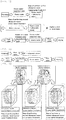
- FIG. 6 is a diagram showing an example of the inventive apparatus for cleaning a semiconductor silicon wafer.
- the first ozone water tank 2 is filled with ozone water, and by immersing a semiconductor silicon wafer W immediately after polishing having a polishing agent adhered to the entire surface thereof, the polishing agent is removed by the ozone water treatment, and at the same time, an oxide film is formed on the surface of the semiconductor silicon wafer.
- the ozone water tank 3 having the ultrasonic wave application means can immerse a vertically-placed semiconductor silicon wafer W in ozone water.
- the ozone water tank has an ultrasonic wave application means for applying ultrasonic waves, the semiconductor silicon wafer can be immersed in the ozone water while applying ultrasonic waves.
- the semiconductor silicon wafer W immersed in ozone water while applying ultrasonic waves is taken out of the ozone water tank 3 having the ultrasonic wave application means and rotated by the wafer rotation means 4, and then is transported to the next tank.
- the tank for immersion is changed every time the semiconductor silicon wafer W is rotated, but it is also possible to immerse the semiconductor silicon wafer W in the same tank.
- the wafer rotation means 4 can rotate the semiconductor silicon wafer W by a predetermined rotation angle with the center of the wafer surface of the semiconductor silicon wafer W as a rotation center.
- the hydrofluoric acid tank 5 is filled with hydrofluoric acid, and the semiconductor silicon wafer W is immersed to remove particles and metal contamination by oxide film removal with the hydrofluoric acid.
- the second ozone water tank 6 is filled with ozone water, and the semiconductor silicon wafer W after immersing in the hydrofluoric acid is immersed in the ozone water, a natural oxide film is formed by the ozone water, and the surface state is finished.
- a polishing agent adhered not only to the wafer surface but also to an edge portion can be removed efficiently by rotating the wafer, and wafer quality can be improved.
- cleaning that is not accompanied by etching of the semiconductor silicon wafer can be performed, and surface roughness and projecting defects can be improved.
- the ozone water filled in the ozone water tanks of the apparatus for cleaning a semiconductor preferably has a concentration of 10 ppm or more.
- the inventive method for cleaning a semiconductor silicon wafer is a method for cleaning a semiconductor silicon wafer for cleaning a semiconductor silicon wafer after polishing, the method including:
- a polishing agent adhered not only to the wafer surface but also to an edge portion can be removed efficiently by rotating the wafer, and wafer quality can be improved.
- FIG. 1 is a diagram showing an example of a flow of the present invention for cleaning a semiconductor silicon wafer after polishing.
- an oxide film is formed by an ozone water treatment of immersing in ozone water on a semiconductor silicon wafer immediately after polishing having a polishing agent adhered to the entire surface thereof (ozone water treatment step after polishing). Then, an ozone water treatment with application of ultrasonic waves (ultrasonic-wave-ozone-water treatment) is performed at room temperature (step of performing a first ultrasonic-wave-ozone-water treatment), and [wafer rotation process ⁇ ultrasonic-wave-ozone-water treatment] (step of performing a second ultrasonic-wave-ozone-water treatment) is performed once or more times. Thus, cleaning is performed.
- a hydrofluoric acid treatment step and an ozone water treatment step are performed.
- the semiconductor silicon wafer is once taken out of the ozone water tank having the ultrasonic wave application means, rotated to a predetermined rotation angle, and then transported to the next tank.
- the rotation angle of the wafer can be rotated by a predetermined rotation angle when the direction of 6 o'clock of the wafer placed vertically inside the ozone water tank having the ultrasonic wave application means is defined as 0°.
- the rotation angle of the wafer at one time is the angle expressed as 360°/(1+n).
- FIG. 3 is a flow diagram showing that the step of performing the second ultrasonic-wave-ozone-water treatment of the present invention is performed twice.
- FIG. 4 is a diagram showing the rotation angles of a semiconductor silicon wafer in a case where the step of performing the second ultrasonic-wave-ozone-water treatment of the present invention is performed twice.
- a wafer rotation process is performed, the wafer is transported to the next ozone water tank having an ultrasonic wave application means, and an ultrasonic-wave-ozone-water treatment is performed again (step of performing a second ultrasonic-wave-ozone-water treatment).
- a wafer rotation process is performed, the wafer is further transported to the next ozone water tank having an ultrasonic wave application means, and an ultrasonic-wave-ozone-water treatment is performed (the second step of performing the second ultrasonic-wave-ozone-water treatment).
- ultrasonic waves can be applied uniformly, not only in the wafer surface, but also in the edge portion, and wafer quality can be further improved.
- the semiconductor silicon wafer after polishing is preferably a semiconductor silicon wafer polished using silica as a polishing agent.
- silica as a polishing agent.
- organic matter can be completely decomposed and removed by the ultrasonic-wave-ozone-water treatments, and silica can also be removed to some extent.
- silica and metal contamination can be eliminated by removing a natural oxide film by a hydrofluoric acid treatment, and lastly, a natural oxide film can be formed by ozone water to finish the surface state.
- a pure water treatment step of immersing the semiconductor silicon wafer in pure water is preferably included, where the pure water treatment step is preferably performed at least before the hydrofluoric acid treatment step. In this manner, wafer quality can be improved more certainly.
- the pure water treatment is not limited thereto, and can be performed between the steps or before and after each step.
- waste liquids of ozone water and pure water are preferably collected and reused. In this manner, waste liquid can be reused, and this leads to cost reduction.
- an ozone water concentration in the steps where ozone water is used is preferably 10 ppm or more. With such an ozone water concentration, a natural oxide film can be formed with certainty, and wafer quality can be improved more certainly.
- the evaluation of the semiconductor silicon wafer in the following Comparative Example and Example was performed by measuring particles on a semiconductor silicon wafer after cleaning, the particles having a diameter of 19 nm or more, by using a wafer inspection apparatus SP5 manufactured by KLA-Tencor Corporation.
- an oxide film was formed on a semiconductor silicon wafer immediately after polishing having an adhered polishing agent by a 180-second ozone water treatment (ozone water treatment step). Then, an ultrasonic-wave-ozone-water treatment with application of ultrasonic waves was performed for 180 seconds (step of performing a first ultrasonic-wave-ozone-water treatment), and [wafer rotation process ⁇ 180-second ultrasonic-wave-ozone-water treatment] (step of performing a second ultrasonic-wave-ozone-water treatment) was performed twice. Thus, cleaning was performed.
- waste liquids of ozone water and pure water out of the waste liquids produced in the steps can be collected and reused.
- the ozone water concentration in the steps where ozone water was used was set to 10 ppm.
- the hydrofluoric acid concentration of the hydrofluoric acid cleaning solution in the hydrofluoric acid treatment step was set to 1.0 mass%.
- a wafer after polishing having an adhered polishing agent was subjected to a pure water treatment, then an SC1 treatment with application of ultrasonic waves was performed for 180 seconds. Subsequently, a pure water treatment, a 180-second hydrofluoric acid treatment, a 180-second ozone water treatment, a pure water treatment, and drying were performed.
- the SC1 cleaning solution used in the SC1 treatment the mixing ratio of ammonia, hydrogen peroxide water, and ultrapure water was set to 1:1:10, and the temperature of the SC1 cleaning solution was set to 80°C.
- the concentrations of the ozone water and the hydrofluoric acid in the hydrofluoric acid treatment and the ozone water treatment were the same as in the Example.
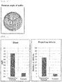
- FIG. 5 is a figure showing the haze and the number of projecting defects in semiconductor silicon wafers after cleaning in the Comparative Example and the Example.
Landscapes
- Cleaning Or Drying Semiconductors (AREA)
- Mechanical Treatment Of Semiconductor (AREA)
Abstract
Description
- The present invention relates to: an apparatus for cleaning a semiconductor silicon wafer; and a method for cleaning a semiconductor silicon wafer.
- Conventionally, when a wafer having a polishing agent adhered to the wafer surface immediately after polishing is cleaned in a batch (cleaned by dipping), it has been common and necessary to perform a cleaning using SC1 (a mixed solution of ammonia water and hydrogen peroxide water) in order to remove organic matter or silica particles contained in the polishing agent, etc.
-
FIG. 2 is a diagram showing an example of a conventional flow for cleaning a semiconductor silicon wafer after polishing. - In a conventional cleaning flow, after removing, from a wafer after polishing, a polishing agent with SC1 and ultrasonic waves, a pure water treatment and removal of particles and metal impurity by oxide film removal using hydrofluoric acid are performed, and after forming an oxide film by reoxidation by ozone water, a pure water treatment is performed, and then drying is performed, as shown in
FIG. 2 . - Patent Document 1:
Japanese Patent Application No. 2015-023069 - However, SC1 is a chemical solution that is accompanied by anisotropic etching, and there have been problems that projecting defects are generated on a wafer surface and that surface roughness is degraded.
- In addition, a chemical like SC1 has a high environmental load and requires wastewater treatment, and requires a temperature adjustment mechanism, and therefore, there has been a problem that costs are extremely high.
- Meanwhile, it is disclosed that in a spin-cleaning method, a neutral aqueous solution of a polymer having a molecular weight of 10,000 or less is supplied to a substrate, the polymer is removed from the substrate, and cleaning is performed with a solution having ozone dissolved (Patent Document 1).
- However, there have been no suggestions of methods for solving the above problems in methods for cleaning in a batch.
- The present invention has been made to solve the above problems, and an object thereof is to provide a method for cleaning a semiconductor silicon wafer and an apparatus for cleaning the same by which the generation of projecting defects on the wafer surface and the degradation of surface roughness in a conventional method for cleaning a semiconductor silicon wafer can be suppressed, and wafer quality can be improved.
- In addition, it is also an object of the present invention to provide a method for cleaning a semiconductor silicon wafer and an apparatus for cleaning the same by which costs can be reduced compared to what is conventional.
- To solve the above problems, the present invention provides
a method for cleaning a semiconductor silicon wafer for cleaning a semiconductor silicon wafer after polishing, the method comprising: - an ozone water treatment step after polishing, of immersing, in ozone water, the semiconductor silicon wafer after polishing;
- a step of performing a first ultrasonic-wave-ozone-water treatment of cleaning the semiconductor silicon wafer at room temperature while immersing in ozone water and applying ultrasonic waves; and
- a step of performing a second ultrasonic-wave-ozone-water treatment of, after the step of performing the first ultrasonic-wave-ozone-water treatment, pulling out the semiconductor silicon wafer from the ozone water, performing a wafer rotation process of rotating, and cleaning the semiconductor silicon wafer after the wafer rotation process again at room temperature while immersing in ozone water and applying ultrasonic waves; wherein
- the step of performing the second ultrasonic-wave-ozone-water treatment is performed once or more times, and subsequently, a hydrofluoric acid treatment step of immersing the semiconductor silicon wafer in hydrofluoric acid and an ozone water treatment step of immersing the semiconductor silicon wafer after the hydrofluoric acid treatment step in ozone water are performed.
- According to such a method for cleaning a semiconductor silicon wafer, a polishing agent adhered not only to the wafer surface but also to an edge portion can be removed efficiently by rotating the wafer, and wafer quality can be improved.
- In addition, since the cleaning is not accompanied by etching of the wafer, surface roughness and projecting defects can be improved.
- Furthermore, since treatment at room temperature is possible by using ozone water, costs can be reduced.
- Furthermore, in this case, when the step of performing the second ultrasonic-wave-ozone-water treatment is performed "n" times, a rotation angle of the semiconductor silicon wafer in the wafer rotation process is preferably 360°/(1+n).
- According to such a cleaning method, ultrasonic waves can be applied uniformly, not only in the wafer surface, but also in the edge portion, and wafer quality can be further improved.
- Furthermore, in this case, the step of performing the second ultrasonic-wave-ozone-water treatment is preferably performed twice.
- According to such a cleaning method, decrease in throughput does not occur in the actual manufacturing process.
- Furthermore, in this case, a pure water treatment step of immersing the semiconductor silicon wafer in pure water is preferably comprised, wherein the pure water treatment step is preferably performed at least before the hydrofluoric acid treatment step.
- According to such a cleaning method, wafer quality can be improved more certainly.
- Furthermore, in this case, out of waste liquids produced in the steps, waste liquids of ozone water and pure water are preferably collected and reused.
- Such a cleaning method leads to cost reduction, since waste liquid can be reused.
- Furthermore, in this case, out of the steps, an ozone water concentration in the steps where ozone water is used is preferably 10 ppm or more.
- According to such a cleaning method, wafer quality can be improved more certainly.
- Furthermore, in this case, the semiconductor silicon wafer after polishing is preferably a semiconductor silicon wafer polished using silica as a polishing agent.
- According to such a cleaning method, not only organic matter but also silica is removed by the steps of performing the first and second ultrasonic-wave-ozone-water treatments, and subsequently, a natural oxide film is removed by the hydrofluoric acid treatment, so that silica and metal contamination can be eliminated. Accordingly, wafer quality can be improved more certainly.
- Furthermore, the present invention provides
an apparatus for cleaning a semiconductor silicon wafer for cleaning a semiconductor silicon wafer after polishing, the apparatus comprising: - a first ozone water tank filled with ozone water for immersing, in the ozone water, the semiconductor silicon wafer after polishing;
- a hydrofluoric acid tank filled with hydrofluoric acid for immersing the semiconductor silicon wafer in the hydrofluoric acid;
- a second ozone water tank filled with ozone water for immersing, in the ozone water, the semiconductor silicon wafer after immersing in the hydrofluoric acid;
- an ozone water tank having an ultrasonic wave application means for immersing the semiconductor silicon wafer in ozone water and cleaning while applying ultrasonic waves; and
- a wafer rotation means for taking the semiconductor silicon wafer out of the ozone water tank having the ultrasonic wave application means and rotating.
- According to such an apparatus for cleaning a semiconductor silicon wafer, a polishing agent adhered not only to the wafer surface but also to an edge portion can be removed efficiently by rotating the wafer, and wafer quality can be improved.
- In addition, cleaning that is not accompanied by etching of the wafer becomes possible, and surface roughness and projecting defects can be improved.
- Furthermore, since treatment at room temperature becomes possible by using ozone water, the apparatus makes it possible to reduce costs.
- Furthermore, in this case, the ozone water filled in the ozone water tanks preferably has a concentration of 10 ppm or more.
- According to such an apparatus for cleaning a semiconductor silicon wafer, wafer quality can be improved more certainly.
- According to the inventive method for cleaning a semiconductor silicon wafer and apparatus for cleaning the same, a polishing agent adhered not only to the wafer surface but also to an edge portion can be removed efficiently by rotating the wafer, and wafer quality can be improved.
- In addition, cleaning that is not accompanied by etching of the wafer becomes possible, and surface roughness and projecting defects can be improved.
- Furthermore, since treatment at room temperature becomes possible by using ozone water, costs can be reduced.
-
-
FIG. 1 is a diagram showing an example of a flow of the present invention for cleaning a semiconductor silicon wafer after polishing. -
FIG. 2 is a diagram showing an example of a conventional flow for cleaning a semiconductor silicon wafer after polishing. -
FIG. 3 is a flow diagram showing a case where a step of performing a second ultrasonic-wave-ozone-water treatment of the present invention is performed twice. -
FIG. 4 is a diagram showing the rotation angles of a semiconductor silicon wafer in a case where the step of performing the second ultrasonic-wave-ozone-water treatment of the present invention is performed twice. -
FIG. 5 is a figure showing the haze and the number of projecting defects in semiconductor silicon wafers after cleaning in the Comparative Example and the Example. -
FIG. 6 is a diagram showing an example of the inventive apparatus for cleaning a semiconductor silicon wafer. - To solve the above problems, the present inventor has earnestly studied and found out that by not using an alkaline chemical solution such as SC1, and by cleaning, with a chemical solution that is not accompanied by etching of silicon, a wafer immediately after polishing having a polishing agent adhered to the entire surface thereof in a state of being at room temperature and pH = 7.0 or less, defects on the wafer can be reduced and degradation of surface roughness can be prevented.
- In addition, the present inventor has found out that by employing a cleaning method (ultrasonic-wave-ozone-water treatment) using both ozone water and ultrasonic waves as a method for removing a polishing agent as a substitute for SC1, and by performing an ozone water treatment multiple times while applying ultrasonic waves with the rotation angle of the wafer changed, it is possible to achieve a surface quality superior to what is conventional.
- Furthermore, the present inventor has found out that an ultrasonic-wave-ozone-water treatment leads to reduction of costs since room temperature treatment and reuse of wastewater are possible, and completed the present invention.
- Hereinafter, the present invention will be specifically described. However, the present invention is not limited thereto.
- Firstly, the inventive apparatus for cleaning a semiconductor silicon wafer will be described.
- The inventive apparatus for cleaning a semiconductor silicon wafer is an apparatus for cleaning a semiconductor silicon wafer for cleaning a semiconductor silicon wafer after polishing, the apparatus including:
- a first ozone water tank filled with ozone water for immersing, in the ozone water, the semiconductor silicon wafer after polishing;
- a hydrofluoric acid tank filled with hydrofluoric acid for immersing the semiconductor silicon wafer in the hydrofluoric acid;
- a second ozone water tank filled with ozone water for immersing, in the ozone water, the semiconductor silicon wafer after immersing in the hydrofluoric acid;
- an ozone water tank having an ultrasonic wave application means for immersing the semiconductor silicon wafer in ozone water and cleaning while applying ultrasonic waves; and
- a wafer rotation means for taking the semiconductor silicon wafer out of the ozone water tank having the ultrasonic wave application means and rotating.
-
FIG. 6 is a diagram showing an example of the inventive apparatus for cleaning a semiconductor silicon wafer. - In the
apparatus 1 for cleaning a semiconductor silicon wafer, the firstozone water tank 2 is filled with ozone water, and by immersing a semiconductor silicon wafer W immediately after polishing having a polishing agent adhered to the entire surface thereof, the polishing agent is removed by the ozone water treatment, and at the same time, an oxide film is formed on the surface of the semiconductor silicon wafer. - The
ozone water tank 3 having the ultrasonic wave application means can immerse a vertically-placed semiconductor silicon wafer W in ozone water. In addition, since the ozone water tank has an ultrasonic wave application means for applying ultrasonic waves, the semiconductor silicon wafer can be immersed in the ozone water while applying ultrasonic waves. - The semiconductor silicon wafer W immersed in ozone water while applying ultrasonic waves is taken out of the
ozone water tank 3 having the ultrasonic wave application means and rotated by the wafer rotation means 4, and then is transported to the next tank. Note that here, there is a plurality ofozone water tanks 3 having the ultrasonic wave application means, and the tank for immersion is changed every time the semiconductor silicon wafer W is rotated, but it is also possible to immerse the semiconductor silicon wafer W in the same tank. - The wafer rotation means 4 can rotate the semiconductor silicon wafer W by a predetermined rotation angle with the center of the wafer surface of the semiconductor silicon wafer W as a rotation center.
- The
hydrofluoric acid tank 5 is filled with hydrofluoric acid, and the semiconductor silicon wafer W is immersed to remove particles and metal contamination by oxide film removal with the hydrofluoric acid. - The second ozone water tank 6 is filled with ozone water, and the semiconductor silicon wafer W after immersing in the hydrofluoric acid is immersed in the ozone water, a natural oxide film is formed by the ozone water, and the surface state is finished.
- According to such an apparatus for cleaning a semiconductor silicon wafer, a polishing agent adhered not only to the wafer surface but also to an edge portion can be removed efficiently by rotating the wafer, and wafer quality can be improved.
- In addition, cleaning that is not accompanied by etching of the semiconductor silicon wafer can be performed, and surface roughness and projecting defects can be improved.
- Furthermore, since treatment at room temperature becomes possible by using ozone water, costs can be reduced.
- Furthermore, the ozone water filled in the ozone water tanks of the apparatus for cleaning a semiconductor preferably has a concentration of 10 ppm or more.
- According to such an apparatus for cleaning a semiconductor silicon wafer, wafer quality can be improved more certainly.
- Next, the inventive method for cleaning a semiconductor silicon wafer will be described.
- The inventive method for cleaning a semiconductor silicon wafer is a method for cleaning a semiconductor silicon wafer for cleaning a semiconductor silicon wafer after polishing, the method including:
- an ozone water treatment step after polishing, of immersing, in ozone water, the semiconductor silicon wafer after polishing;
- a step of performing a first ultrasonic-wave-ozone-water treatment of cleaning the semiconductor silicon wafer at room temperature while immersing in ozone water and applying ultrasonic waves; and
- a step of performing a second ultrasonic-wave-ozone-water treatment of, after the step of performing the first ultrasonic-wave-ozone-water treatment, pulling out the semiconductor silicon wafer from the ozone water, performing a wafer rotation process of rotating, and cleaning the semiconductor silicon wafer after the wafer rotation process again at room temperature while immersing in ozone water and applying ultrasonic waves; wherein
- the step of performing the second ultrasonic-wave-ozone-water treatment is performed once or more times, and subsequently, a hydrofluoric acid treatment step of immersing the semiconductor silicon wafer in hydrofluoric acid and an ozone water treatment step of immersing the semiconductor silicon wafer after the hydrofluoric acid treatment step in ozone water are performed.
- According to such a method for cleaning a semiconductor silicon wafer, a polishing agent adhered not only to the wafer surface but also to an edge portion can be removed efficiently by rotating the wafer, and wafer quality can be improved.
- In addition, since the cleaning is not accompanied by etching of the wafer, surface roughness and projecting defects can be improved.
- Furthermore, since treatment at room temperature is possible by using ozone water, costs can be reduced.
-
FIG. 1 is a diagram showing an example of a flow of the present invention for cleaning a semiconductor silicon wafer after polishing. - As shown in
FIG. 1 , an oxide film is formed by an ozone water treatment of immersing in ozone water on a semiconductor silicon wafer immediately after polishing having a polishing agent adhered to the entire surface thereof (ozone water treatment step after polishing). Then, an ozone water treatment with application of ultrasonic waves (ultrasonic-wave-ozone-water treatment) is performed at room temperature (step of performing a first ultrasonic-wave-ozone-water treatment), and [wafer rotation process → ultrasonic-wave-ozone-water treatment] (step of performing a second ultrasonic-wave-ozone-water treatment) is performed once or more times. Thus, cleaning is performed. Subsequently, a hydrofluoric acid treatment step and an ozone water treatment step are performed. In addition, it is possible to perform a pure water treatment step before the hydrofluoric acid treatment step, a pure water treatment step after the ozone water treatment step, and drying. - In the wafer rotation process, the semiconductor silicon wafer is once taken out of the ozone water tank having the ultrasonic wave application means, rotated to a predetermined rotation angle, and then transported to the next tank.
- The greater the number of times to repeat the step of performing the second ultrasonic-wave-ozone-water treatment, the more the wafer quality is improved. However, when performed twice, decrease in throughput does not occur in the actual manufacturing process. Therefore, it is desirable to perform the step of performing the second ultrasonic-wave-ozone-water treatment twice.
- The rotation angle of the wafer can be rotated by a predetermined rotation angle when the direction of 6 o'clock of the wafer placed vertically inside the ozone water tank having the ultrasonic wave application means is defined as 0°.
- Furthermore, when the step of performing the second ultrasonic-wave-ozone-water treatment is performed "n" times, it is desirable for the rotation angle of the wafer at one time to be the angle expressed as 360°/(1+n).
-
FIG. 3 is a flow diagram showing that the step of performing the second ultrasonic-wave-ozone-water treatment of the present invention is performed twice.FIG. 4 is a diagram showing the rotation angles of a semiconductor silicon wafer in a case where the step of performing the second ultrasonic-wave-ozone-water treatment of the present invention is performed twice. - As shown in
FIG. 3 , after performing an ultrasonic-wave-ozone-water treatment (step of performing a first ultrasonic-wave-ozone-water treatment), a wafer rotation process is performed, the wafer is transported to the next ozone water tank having an ultrasonic wave application means, and an ultrasonic-wave-ozone-water treatment is performed again (step of performing a second ultrasonic-wave-ozone-water treatment). Subsequently, a wafer rotation process is performed, the wafer is further transported to the next ozone water tank having an ultrasonic wave application means, and an ultrasonic-wave-ozone-water treatment is performed (the second step of performing the second ultrasonic-wave-ozone-water treatment). - Furthermore, when the step of performing the second ultrasonic-wave-ozone-water treatment is performed twice, the rotation angle in one wafer rotation process can be 360°/(1+2) = 120° as shown in
FIGS. 3 and4 . - By performing such a step of performing the second ultrasonic-wave-ozone-water treatment repeatedly, ultrasonic waves can be applied uniformly, not only in the wafer surface, but also in the edge portion, and wafer quality can be further improved.
- Furthermore, the semiconductor silicon wafer after polishing is preferably a semiconductor silicon wafer polished using silica as a polishing agent. In this manner, organic matter can be completely decomposed and removed by the ultrasonic-wave-ozone-water treatments, and silica can also be removed to some extent. Thereafter, silica and metal contamination can be eliminated by removing a natural oxide film by a hydrofluoric acid treatment, and lastly, a natural oxide film can be formed by ozone water to finish the surface state.
- Furthermore, a pure water treatment step of immersing the semiconductor silicon wafer in pure water is preferably included, where the pure water treatment step is preferably performed at least before the hydrofluoric acid treatment step. In this manner, wafer quality can be improved more certainly. As a matter of course, the pure water treatment is not limited thereto, and can be performed between the steps or before and after each step.
- Furthermore, out of waste liquids produced in the steps, waste liquids of ozone water and pure water are preferably collected and reused. In this manner, waste liquid can be reused, and this leads to cost reduction.
- Furthermore, out of the steps, an ozone water concentration in the steps where ozone water is used is preferably 10 ppm or more. With such an ozone water concentration, a natural oxide film can be formed with certainty, and wafer quality can be improved more certainly.
- Hereinafter, the present invention will be more specifically described with reference to an Example and a Comparative Example. However, the present invention is not limited to these Examples.
- The evaluation of the semiconductor silicon wafer in the following Comparative Example and Example was performed by measuring particles on a semiconductor silicon wafer after cleaning, the particles having a diameter of 19 nm or more, by using a wafer inspection apparatus SP5 manufactured by KLA-Tencor Corporation.
- According to the cleaning flow shown in
FIG. 1 , an oxide film was formed on a semiconductor silicon wafer immediately after polishing having an adhered polishing agent by a 180-second ozone water treatment (ozone water treatment step). Then, an ultrasonic-wave-ozone-water treatment with application of ultrasonic waves was performed for 180 seconds (step of performing a first ultrasonic-wave-ozone-water treatment), and [wafer rotation process → 180-second ultrasonic-wave-ozone-water treatment] (step of performing a second ultrasonic-wave-ozone-water treatment) was performed twice. Thus, cleaning was performed. Subsequently, a pure water treatment, a 180-second hydrofluoric acid treatment step, a 180-second ozone water treatment step, a pure water treatment, and drying were performed in this order. In addition, all the steps in the Example were performed at room temperature. - The number of times of repeating the step of performing the second ultrasonic-wave-ozone-water treatment was two, and therefore, the rotation angle of the semiconductor silicon wafer at one time was 360/(1+2) = 120°.
- In addition, in the Example, waste liquids of ozone water and pure water out of the waste liquids produced in the steps can be collected and reused.
- Out of the steps in the Example, the ozone water concentration in the steps where ozone water was used was set to 10 ppm. In addition, the hydrofluoric acid concentration of the hydrofluoric acid cleaning solution in the hydrofluoric acid treatment step was set to 1.0 mass%.
- According to the cleaning flow shown in
FIG. 2 , a wafer after polishing having an adhered polishing agent was subjected to a pure water treatment, then an SC1 treatment with application of ultrasonic waves was performed for 180 seconds. Subsequently, a pure water treatment, a 180-second hydrofluoric acid treatment, a 180-second ozone water treatment, a pure water treatment, and drying were performed. In the SC1 cleaning solution used in the SC1 treatment, the mixing ratio of ammonia, hydrogen peroxide water, and ultrapure water was set to 1:1:10, and the temperature of the SC1 cleaning solution was set to 80°C. In addition, the concentrations of the ozone water and the hydrofluoric acid in the hydrofluoric acid treatment and the ozone water treatment were the same as in the Example. -
FIG. 5 is a figure showing the haze and the number of projecting defects in semiconductor silicon wafers after cleaning in the Comparative Example and the Example. - As shown in
FIG. 5 , when comparing the case where the cleaning was performed under common cleaning conditions using SC1 (Comparative Example) and the case where the cleaning was performed using ozone water and ultrasonic waves (Example), the haze and the number of projecting defects were both reduced and improved in the Example. - In addition, LLS (Localized Light Scatterers) were also reduced and improved in the Example compared with the Comparative Example.
- It should be noted that the present invention is not limited to the above-described embodiments. The embodiments are just examples, and any examples that have substantially the same feature and demonstrate the same functions and effects as those in the technical concept disclosed in claims of the present invention are included in the technical scope of the present invention.
Claims (9)
- A method for cleaning a semiconductor silicon wafer for cleaning a semiconductor silicon wafer after polishing, the method comprising:an ozone water treatment step after polishing, of immersing, in ozone water, the semiconductor silicon wafer after polishing;a step of performing a first ultrasonic-wave-ozone-water treatment of cleaning the semiconductor silicon wafer at room temperature while immersing in ozone water and applying ultrasonic waves; anda step of performing a second ultrasonic-wave-ozone-water treatment of, after the step of performing the first ultrasonic-wave-ozone-water treatment, pulling out the semiconductor silicon wafer from the ozone water, performing a wafer rotation process of rotating, and cleaning the semiconductor silicon wafer after the wafer rotation process again at room temperature while immersing in ozone water and applying ultrasonic waves; whereinthe step of performing the second ultrasonic-wave-ozone-water treatment is performed once or more times, and subsequently, a hydrofluoric acid treatment step of immersing the semiconductor silicon wafer in hydrofluoric acid and an ozone water treatment step of immersing the semiconductor silicon wafer after the hydrofluoric acid treatment step in ozone water are performed.
- The method for cleaning a semiconductor silicon wafer according to claim 1, wherein when the step of performing the second ultrasonic-wave-ozone-water treatment is performed "n" times, a rotation angle of the semiconductor silicon wafer in the wafer rotation process is 360°/(l+n).
- The method for cleaning a semiconductor silicon wafer according to claim 1 or 2, wherein the step of performing the second ultrasonic-wave-ozone-water treatment is performed twice.
- The method for cleaning a semiconductor silicon wafer according to any one of claims 1 to 3, comprising a pure water treatment step of immersing the semiconductor silicon wafer in pure water, wherein the pure water treatment step is performed at least before the hydrofluoric acid treatment step.
- The method for cleaning a semiconductor silicon wafer according to claim 4, wherein out of waste liquids produced in the steps, waste liquids of ozone water and pure water are collected and reused.
- The method for cleaning a semiconductor silicon wafer according to any one of claims 1 to 5, wherein out of the steps, an ozone water concentration in the steps where ozone water is used is 10 ppm or more.
- The method for cleaning a semiconductor silicon wafer according to any one of claims 1 to 6, wherein the semiconductor silicon wafer after polishing is a semiconductor silicon wafer polished using silica as a polishing agent.
- An apparatus for cleaning a semiconductor silicon wafer for cleaning a semiconductor silicon wafer after polishing, the apparatus comprising:a first ozone water tank filled with ozone water for immersing, in the ozone water, the semiconductor silicon wafer after polishing;a hydrofluoric acid tank filled with hydrofluoric acid for immersing the semiconductor silicon wafer in the hydrofluoric acid;a second ozone water tank filled with ozone water for immersing, in the ozone water, the semiconductor silicon wafer after immersing in the hydrofluoric acid;an ozone water tank having an ultrasonic wave application means for immersing the semiconductor silicon wafer in ozone water and cleaning while applying ultrasonic waves; anda wafer rotation means for taking the semiconductor silicon wafer out of the ozone water tank having the ultrasonic wave application means and rotating.
- The apparatus for cleaning a semiconductor silicon wafer according to claim 8, wherein the ozone water filled in the ozone water tanks has a concentration of 10 ppm or more.
Applications Claiming Priority (2)
| Application Number | Priority Date | Filing Date | Title |
|---|---|---|---|
| JP2018192672A JP6988761B2 (en) | 2018-10-11 | 2018-10-11 | Cleaning processing equipment and cleaning method for semiconductor silicon wafers |
| PCT/JP2019/036261 WO2020075448A1 (en) | 2018-10-11 | 2019-09-17 | Semiconductor silicon wafer cleaning treatment apparatus and cleaning method |
Publications (3)
| Publication Number | Publication Date |
|---|---|
| EP3866185A1 true EP3866185A1 (en) | 2021-08-18 |
| EP3866185A4 EP3866185A4 (en) | 2022-07-13 |
| EP3866185B1 EP3866185B1 (en) | 2026-05-06 |
Family
ID=70163677
Family Applications (1)
| Application Number | Title | Priority Date | Filing Date |
|---|---|---|---|
| EP19871349.7A Active EP3866185B1 (en) | 2018-10-11 | 2019-09-17 | Semiconductor silicon wafer cleaning treatment apparatus and cleaning method |
Country Status (7)
| Country | Link |
|---|---|
| US (1) | US12272542B2 (en) |
| EP (1) | EP3866185B1 (en) |
| JP (1) | JP6988761B2 (en) |
| KR (1) | KR102762060B1 (en) |
| CN (1) | CN112673458B (en) |
| TW (1) | TWI799651B (en) |
| WO (1) | WO2020075448A1 (en) |
Families Citing this family (6)
| Publication number | Priority date | Publication date | Assignee | Title |
|---|---|---|---|---|
| JP7020507B2 (en) * | 2020-04-28 | 2022-02-16 | 信越半導体株式会社 | Cleaning method for semiconductor wafers |
| JP7422606B2 (en) * | 2020-05-25 | 2024-01-26 | 東京エレクトロン株式会社 | Substrate processing equipment and substrate processing method |
| CN113223934A (en) * | 2021-04-30 | 2021-08-06 | 苏州协鑫光伏科技有限公司 | Cleaning method of 210 large-size silicon wafer |
| EP4266353A1 (en) * | 2022-04-20 | 2023-10-25 | Siltronic AG | Method for cleaning a semiconductor wafer after polishing by means of cmp in a cleaning line |
| CN114864744B (en) * | 2022-05-05 | 2024-04-02 | 普乐新能源科技(泰兴)有限公司 | Efficient cleaning method and system for nano silicon slurry |
| CN115020199A (en) * | 2022-06-28 | 2022-09-06 | 上海华力集成电路制造有限公司 | Method for improving GOI performance through O3 processing |
Family Cites Families (15)
| Publication number | Priority date | Publication date | Assignee | Title |
|---|---|---|---|---|
| JPH08107100A (en) * | 1994-10-06 | 1996-04-23 | Sony Corp | Chemical treatment method and chemical treatment device |
| JP2000164552A (en) | 1998-11-24 | 2000-06-16 | Dainippon Screen Mfg Co Ltd | Device and method for substrate processing |
| JP2001102343A (en) * | 1999-09-28 | 2001-04-13 | Sony Corp | Semiconductor wafer cleaning method |
| JP2003010795A (en) * | 2001-06-29 | 2003-01-14 | Sekisui Chem Co Ltd | Substrate cleaning apparatus and cleaning method |
| DE10239773B3 (en) | 2002-08-29 | 2004-02-26 | Wacker Siltronic Ag | Cleaning a semiconductor wafer comprises treating the wafer under megasound with an aqueous solution containing ozone, and treating the wafer with an aqueous solution containing hydrofluoric acid and hydrochloric acid |
| KR100590268B1 (en) | 2004-05-03 | 2006-06-19 | 삼성에스디아이 주식회사 | Manufacturing Method of Semiconductor Device |
| JP4827587B2 (en) | 2006-03-31 | 2011-11-30 | Sumco Techxiv株式会社 | Silicon wafer manufacturing method |
| KR20100049856A (en) | 2008-11-04 | 2010-05-13 | 주식회사 실트론 | Method for cleaning a substrate |
| JP5181100B2 (en) * | 2009-04-09 | 2013-04-10 | 東京エレクトロン株式会社 | Substrate processing apparatus, substrate processing method, and storage medium |
| US8668777B2 (en) * | 2010-12-22 | 2014-03-11 | Lam Research Ag | Process for treating a semiconductor wafer |
| CN104380091B (en) | 2012-06-28 | 2016-06-22 | 西门子医疗保健诊断公司 | The reader equipment of signal amplification and method |
| JP2015023069A (en) | 2013-07-17 | 2015-02-02 | 株式会社Screenホールディングス | Substrate cleaning apparatus and substrate cleaning method |
| CN104157766A (en) * | 2014-08-06 | 2014-11-19 | 韩忠贺 | High-temperature etching method for galium arsenide substrate of chip |
| JP6610443B2 (en) * | 2016-06-07 | 2019-11-27 | 信越半導体株式会社 | Surface defect inspection method for semiconductor silicon wafer |
| JP2018107338A (en) * | 2016-12-27 | 2018-07-05 | 株式会社Sumco | Cleaning method of wafer |
-
2018
- 2018-10-11 JP JP2018192672A patent/JP6988761B2/en active Active
-
2019
- 2019-09-17 CN CN201980058971.2A patent/CN112673458B/en active Active
- 2019-09-17 EP EP19871349.7A patent/EP3866185B1/en active Active
- 2019-09-17 US US17/275,145 patent/US12272542B2/en active Active
- 2019-09-17 KR KR1020217008258A patent/KR102762060B1/en active Active
- 2019-09-17 WO PCT/JP2019/036261 patent/WO2020075448A1/en not_active Ceased
- 2019-10-02 TW TW108135616A patent/TWI799651B/en active
Also Published As
| Publication number | Publication date |
|---|---|
| CN112673458B (en) | 2025-02-25 |
| US20220059343A1 (en) | 2022-02-24 |
| EP3866185A4 (en) | 2022-07-13 |
| KR20210068017A (en) | 2021-06-08 |
| KR102762060B1 (en) | 2025-02-05 |
| CN112673458A (en) | 2021-04-16 |
| US12272542B2 (en) | 2025-04-08 |
| WO2020075448A1 (en) | 2020-04-16 |
| EP3866185B1 (en) | 2026-05-06 |
| JP2020061483A (en) | 2020-04-16 |
| JP6988761B2 (en) | 2022-01-05 |
| TWI799651B (en) | 2023-04-21 |
| TW202044396A (en) | 2020-12-01 |
Similar Documents
| Publication | Publication Date | Title |
|---|---|---|
| US12272542B2 (en) | Apparatus for cleaning semiconductor silicon wafer and method for cleaning semiconductor silicon wafer | |
| US5954885A (en) | Cleaning method | |
| JP3154814B2 (en) | Semiconductor wafer cleaning method and cleaning apparatus | |
| TWI404134B (en) | Method for manufacturing semiconductor device and method for reducing micro roughness on semiconductor surface | |
| EP0718873A2 (en) | Cleaning process for hydrophobic silicon wafers | |
| US11862456B2 (en) | Method for cleaning semiconductor wafer | |
| JP2008103701A (en) | Wet treatment method of silicon wafer | |
| JP6575643B2 (en) | Silicon wafer manufacturing method | |
| KR20100049856A (en) | Method for cleaning a substrate | |
| KR20230173091A (en) | Wafer cleaning method and cleaning processing device | |
| US7731801B2 (en) | Semiconductor wafer treatment method and apparatus therefor | |
| JP4817887B2 (en) | Semiconductor substrate cleaning method | |
| CN119054053A (en) | Cleaning liquid and wafer cleaning method | |
| JP2024078489A (en) | Method for removing device patterns and method for evaluating crystal defects in silicon wafers using this method | |
| CN118435324A (en) | Semiconductor wafer cleaning method and semiconductor wafer manufacturing method | |
| JP3595681B2 (en) | Manufacturing method of epitaxial wafer | |
| JP7279753B2 (en) | Silicon wafer cleaning method and manufacturing method | |
| CN118142948A (en) | A cleaning machine and a cleaning process for semiconductor silicon wafer | |
| JP2022166590A (en) | Wafer cleaning method | |
| JP2006351736A (en) | Semiconductor substrate cleaning method | |
| JPH02235337A (en) | Treating method of semiconductor substrate | |
| WO2017217186A1 (en) | Silicon wafer transfer/storage method |
Legal Events
| Date | Code | Title | Description |
|---|---|---|---|
| STAA | Information on the status of an ep patent application or granted ep patent |
Free format text: STATUS: THE INTERNATIONAL PUBLICATION HAS BEEN MADE |
|
| PUAI | Public reference made under article 153(3) epc to a published international application that has entered the european phase |
Free format text: ORIGINAL CODE: 0009012 |
|
| STAA | Information on the status of an ep patent application or granted ep patent |
Free format text: STATUS: REQUEST FOR EXAMINATION WAS MADE |
|
| 17P | Request for examination filed |
Effective date: 20210309 |
|
| AK | Designated contracting states |
Kind code of ref document: A1 Designated state(s): AL AT BE BG CH CY CZ DE DK EE ES FI FR GB GR HR HU IE IS IT LI LT LU LV MC MK MT NL NO PL PT RO RS SE SI SK SM TR |
|
| DAV | Request for validation of the european patent (deleted) | ||
| DAX | Request for extension of the european patent (deleted) | ||
| A4 | Supplementary search report drawn up and despatched |
Effective date: 20220615 |
|
| RIC1 | Information provided on ipc code assigned before grant |
Ipc: H01L 21/67 20060101ALN20220610BHEP Ipc: H01L 21/306 20060101ALI20220610BHEP Ipc: H01L 21/02 20060101AFI20220610BHEP |
|
| REG | Reference to a national code |
Ref legal event code: R079 Free format text: PREVIOUS MAIN CLASS: H01L0021304000 Ref country code: DE Ref legal event code: R079 Ref document number: 602019084695 Country of ref document: DE Free format text: PREVIOUS MAIN CLASS: H01L0021304000 Ipc: H01L0021020000 |
|
| GRAJ | Information related to disapproval of communication of intention to grant by the applicant or resumption of examination proceedings by the epo deleted |
Free format text: ORIGINAL CODE: EPIDOSDIGR1 |
|
| GRAP | Despatch of communication of intention to grant a patent |
Free format text: ORIGINAL CODE: EPIDOSNIGR1 |
|
| RIC1 | Information provided on ipc code assigned before grant |
Ipc: H01L 21/02 20060101AFI20251111BHEP Ipc: H01L 21/306 20060101ALI20251111BHEP Ipc: H01L 21/67 20060101ALN20251111BHEP |
|
| GRAP | Despatch of communication of intention to grant a patent |
Free format text: ORIGINAL CODE: EPIDOSNIGR1 |
|
| STAA | Information on the status of an ep patent application or granted ep patent |
Free format text: STATUS: GRANT OF PATENT IS INTENDED |
|
| RIC1 | Information provided on ipc code assigned before grant |
Ipc: H01L 21/02 20060101AFI20251208BHEP Ipc: H01L 21/306 20060101ALI20251208BHEP Ipc: H01L 21/67 20060101ALN20251208BHEP |
|
| INTG | Intention to grant announced |
Effective date: 20251218 |
|
| GRAS | Grant fee paid |
Free format text: ORIGINAL CODE: EPIDOSNIGR3 |
|
| GRAA | (expected) grant |
Free format text: ORIGINAL CODE: 0009210 |
|
| STAA | Information on the status of an ep patent application or granted ep patent |
Free format text: STATUS: THE PATENT HAS BEEN GRANTED |
|
| AK | Designated contracting states |
Kind code of ref document: B1 Designated state(s): AL AT BE BG CH CY CZ DE DK EE ES FI FR GB GR HR HU IE IS IT LI LT LU LV MC MK MT NL NO PL PT RO RS SE SI SK SM TR |
|
| REG | Reference to a national code |
Ref country code: CH Ref legal event code: F10 Free format text: ST27 STATUS EVENT CODE: U-0-0-F10-F00 (AS PROVIDED BY THE NATIONAL OFFICE) Effective date: 20260506 Ref country code: GB Ref legal event code: FG4D |