EP3859785A1 - Display substrate and manufacturing method therefor, and display apparatus - Google Patents
Display substrate and manufacturing method therefor, and display apparatus Download PDFInfo
- Publication number
- EP3859785A1 EP3859785A1 EP19858713.1A EP19858713A EP3859785A1 EP 3859785 A1 EP3859785 A1 EP 3859785A1 EP 19858713 A EP19858713 A EP 19858713A EP 3859785 A1 EP3859785 A1 EP 3859785A1
- Authority
- EP
- European Patent Office
- Prior art keywords
- layer
- insulating layer
- conductive wire
- interlayer dielectric
- trench
- Prior art date
- Legal status (The legal status is an assumption and is not a legal conclusion. Google has not performed a legal analysis and makes no representation as to the accuracy of the status listed.)
- Pending
Links
Images




Classifications
-
- H—ELECTRICITY
- H10—SEMICONDUCTOR DEVICES; ELECTRIC SOLID-STATE DEVICES NOT OTHERWISE PROVIDED FOR
- H10K—ORGANIC ELECTRIC SOLID-STATE DEVICES
- H10K59/00—Integrated devices, or assemblies of multiple devices, comprising at least one organic light-emitting element covered by group H10K50/00
- H10K59/10—OLED displays
- H10K59/12—Active-matrix OLED [AMOLED] displays
- H10K59/131—Interconnections, e.g. wiring lines or terminals
- H10K59/1315—Interconnections, e.g. wiring lines or terminals comprising structures specially adapted for lowering the resistance
-
- H—ELECTRICITY
- H10—SEMICONDUCTOR DEVICES; ELECTRIC SOLID-STATE DEVICES NOT OTHERWISE PROVIDED FOR
- H10K—ORGANIC ELECTRIC SOLID-STATE DEVICES
- H10K59/00—Integrated devices, or assemblies of multiple devices, comprising at least one organic light-emitting element covered by group H10K50/00
- H10K59/10—OLED displays
- H10K59/12—Active-matrix OLED [AMOLED] displays
- H10K59/1201—Manufacture or treatment
-
- H—ELECTRICITY
- H10—SEMICONDUCTOR DEVICES; ELECTRIC SOLID-STATE DEVICES NOT OTHERWISE PROVIDED FOR
- H10K—ORGANIC ELECTRIC SOLID-STATE DEVICES
- H10K59/00—Integrated devices, or assemblies of multiple devices, comprising at least one organic light-emitting element covered by group H10K50/00
- H10K59/10—OLED displays
- H10K59/12—Active-matrix OLED [AMOLED] displays
- H10K59/131—Interconnections, e.g. wiring lines or terminals
-
- H—ELECTRICITY
- H10—SEMICONDUCTOR DEVICES; ELECTRIC SOLID-STATE DEVICES NOT OTHERWISE PROVIDED FOR
- H10K—ORGANIC ELECTRIC SOLID-STATE DEVICES
- H10K71/00—Manufacture or treatment specially adapted for the organic devices covered by this subclass
-
- H—ELECTRICITY
- H10—SEMICONDUCTOR DEVICES; ELECTRIC SOLID-STATE DEVICES NOT OTHERWISE PROVIDED FOR
- H10K—ORGANIC ELECTRIC SOLID-STATE DEVICES
- H10K71/00—Manufacture or treatment specially adapted for the organic devices covered by this subclass
- H10K71/621—Providing a shape to conductive layers, e.g. patterning or selective deposition
Definitions
- the present disclosure relates to the field of display technology, and in particular, to a display substrate, a method of manufacturing the same, and a display device.
- Existing organic light emitting devices include an active matrix (abbreviated as AM) manner or a passive matrix (abbreviated as PM) manner.
- AM active matrix
- PM passive matrix
- a resistance value of a conductive wire In order to make the resistance value of the conductive wire small, a wide conductive wire is usually used.
- the conductive wire is generally arranged in a non-display area of a display screen. An excessively wide conductive wire will increase an area of the non-display area, which is not conducive to the realization of a display device with a narrow frame.
- Some embodiments of the present disclosure provide a display substrate comprising: a base substrate comprising a peripheral area; and a conductive wire disposed on the base substrate and located in the peripheral area, wherein the conductive wire comprises: a first portion extending in a first direction parallel to an upper surface of the base substrate; and a second portion extending in a second direction perpendicular to the upper surface of the base substrate.
- the wire comprises at least two second portions.
- the conductive wire further comprises a third portion extending in the first direction, and the second portion connects the first portion with the third portion.
- the conductive wire comprises at least one conductive wire sub-portion, and each conductive wire sub-portion comprises a first segment, a second segment, a third segment, a fourth segment and a fifth segment connected in sequence; and wherein the first segment and fifth segment constitute the first portion, the second segment and the fourth segment constitute the second portion, and the third segment constitutes the third portion.
- the conductive wire comprises a plurality of conductive wire sub-portions, and the plurality of conductive wire sub-portions are periodically arranged.
- the display substrate further comprising: an interlayer dielectric layer disposed on the base substrate and located in the peripheral area; and a trench in the interlayer dielectric layer, wherein the first portion is located on a bottom of the trench, the second portion is located on a sidewall of the trench, and the third portion is located on the interlayer dielectric layer.
- the trench penetrates the interlayer dielectric layer in the second direction.
- the display substrate further comprising: a first insulating layer disposed on the base substrate and located in the peripheral area; an interlayer dielectric layer disposed on the first insulating layer and located in the peripheral area; and a trench formed in both the first insulating layer and the interlayer dielectric layer, wherein the first portion is located on a bottom of the trench, the second portion is located on a sidewall of the trench, and the third portion is located on the interlayer dielectric layer.
- the trench penetrates both the first insulating layer and the interlayer dielectric layer in the second direction.
- the display substrate further comprising: a first insulating layer disposed on the base substrate and located in the peripheral area; a second insulating layer disposed on the first insulating layer and located in the peripheral area; an interlayer dielectric layer disposed on the second insulating layer and located in the peripheral area; and a trench formed in all of the first insulating layer, the second insulating layer, and the interlayer dielectric layer, wherein the first portion is located on a bottom of the trench, the second portion is located on a sidewall of the trench, and the third portion is located on the interlayer dielectric layer.
- the trench penetrates all of the first insulating layer, the second insulating layer and the interlayer dielectric layer in the second direction.
- the display substrate further comprising: a buffer layer disposed on the base substrate and located in the peripheral area; a first insulating layer disposed on the buffer layer and located in the peripheral area; a second insulating layer disposed on the first insulating layer and located in the peripheral area; an interlayer dielectric layer disposed on the second insulating layer and located in the peripheral area; and a trench formed in all of the buffer layer, the first insulating layer, the second insulating layer and the interlayer dielectric layer, wherein the first portion is located on a bottom of the trench, the second portion is located on a sidewall of the trench, and the third portion is located on the interlayer dielectric layer.
- the trench penetrates all of the buffer layer, the first insulating layer, the second insulating layer, and the interlayer dielectric layer in the second direction.
- the display substrate further comprising: a barrier layer disposed on the base substrate and located in the peripheral area; a buffer layer disposed on the barrier layer and located in the peripheral area; a first insulating layer disposed on the buffer layer and located in the peripheral area; a second insulating layer disposed on the first insulating layer and located in the peripheral area; an interlayer dielectric layer disposed on the second insulating layer and located in the peripheral area; and a trench formed in all of the barrier layer, the buffer layer, the first insulating layer, the second insulating layer and the interlayer dielectric layer, wherein the first portion is located on a bottom of the trench, the second portion is located on a sidewall of the trench, and the third portion is located on the interlayer dielectric layer.
- the trench penetrates all of the barrier layer, the buffer layer, the first insulating layer, the second insulating layer, and the interlayer dielectric layer.
- the number of the trench is at least two.
- a ratio of a height of the second portion in the second direction to a sum of a width of the first portion in the first direction and the height of the second portion in the second direction is greater than or equal to 1/13.
- the base substrate further comprises a middle area, the peripheral area surrounding the middle area, the display substrate further comprises: a thin film transistor disposed on the base substrate and located in the middle area, the thin film transistor comprising a source-drain layer, wherein the conductive wire and the source-drain layer are located in the same layer and formed of the same material.
- the display substrate further comprising: an organic light emitting device disposed on the base substrate and located in the middle area, the organic light emitting device comprising an anode, a cathode, and a light emitting layer between the anode and the cathode; and a conductive layer disposed on the conductive wire and located in the peripheral area, wherein the conductive layer electrically connects the cathode with the conductive wire.
- the conductive layer and the anode are located in the same layer and formed of the same material.
- the display substrate further comprising a common electrode disposed on the base substrate and located in the middle area, wherein the conductive wire is electrically connected to the common electrode.
- Some embodiments of the present disclosure provide a display device comprising the display substrate according to the above embodiments.
- Some embodiments of the present disclosure provide a method of manufacturing a display substrate, comprising the following steps: providing a base substrate comprising a peripheral area; forming an insulating layer in the peripheral area; forming at least one trench in the insulating layer; and forming a conductive wire in the trench and on the insulating layer, so that the conductive wire comprises: a first portion located on a bottom of the trench; and a second portion located on a sidewall of the trench.
- first a first component, a first member, a first element, a first region, a first layer, and/or a first portion discussed below may be referred to as a second component, a second member, a second element, a second region, a second layer, and/or second portion without departing from the teachings of the present disclosure.
- insulating layer may be used as their common name, that is, the expression “insulating layer” may include at least one of the barrier layer, the buffer layer, the first insulating layer, the second insulating layer and the interlayer dielectric layers.
- the expression “insulating layer” may include the interlayer dielectric layer; or the expression “insulating layer” may include two layers of the interlayer dielectric layer and one of the first insulating layer and a second insulating layer; or the expression “insulating layer” may include three layers of the first insulating layer, the second insulating layer, and the interlayer dielectric layer; or the expression “insulating layer” may include four layers of the buffer layer, the first insulating layer, and the second insulating layer and the interlayer dielectric layer; or the expression “insulating layer” may include five layers of the barrier layer, the buffer layer, the first insulating layer, the second insulating layer, and the interlayer dielectric layer.
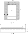
- FIGS. 1A and 1B a display substrate in the related art is shown, and in particular, a conductive wire of the display substrate in the related art is shown.
- FIG. 1A is a plan view of the display substrate
- FIG. 1B is a cross-sectional view taken along a B-B' direction in FIG. 1A .
- the display substrate includes a base substrate 10 including a middle area AA and a peripheral area NA surrounding the middle area AA.
- the middle area AA corresponds to a display area, which is used for displaying image, of a display device including the display substrate
- the peripheral area corresponds to a non-display area of the display device.
- the middle area AA is referred to as a display area AA of the base substrate 10 and/or the display substrate
- the peripheral area is referred to as a non-display area NA of the base substrate 10 and/or the display substrate.
- the display substrate further includes: an insulating layer 12 disposed on the base substrate 10 and located at least in the non-display area NA; and a conductive wire 14 disposed on the insulating layer 12 and located in the non-display area NA.
- the insulating layer 12 may be an interlayer dielectric layer.
- the conductive wire 14 are completely laid on the insulating layer 12.
- a width of the conductive wire 14 (i.e., a width w indicated in the figure)
- the conductive wire 14 may be a cathode conductive wire (i.e., a VSS conductive wire)
- the width w of the conductive wire 14 is generally 200 ⁇ m or more.
- the wide conductive wire 14 needs to occupy a large space in the non-display area, which is not conducive to the realization of a display device with a narrow frame.
- some embodiments of the present disclosure provide a display substrate.
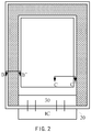
- FIG. 2 a plan view of a display substrate according to some embodiments of the present disclosure is shown.
- the display substrate includes a base substrate 20 including a display area AA and a non-display area NA surrounding the display area AA.
- an OLED display device is taken as an example to describe the display substrate according to some embodiments of the present disclosure.
- the embodiments of the present disclosure are not limited to the OLED display device.
- the display substrate includes: a plurality of organic light emitting devices located in the display area AA; and a conductive wire located in the non-display area NA.
- the organic light emitting devices and the conductive wire will be described in more detail below with reference to the drawings.
- the display substrate further includes: an electrical connection portion (pad) 30 located in the non-display area NA.
- the electrical connection portion 30 may be electrically connected to an integrated circuit IC, and the conductive wire is used to electrically connect an electrode (such as a cathode) of the organic light emitting device to the electrical connection portion 30, and then to the integrated circuit IC.
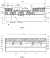
- FIG. 3 is a cross-sectional view taken along the B-B' direction in FIG. 2 , which shows a cross-sectional structure of the non-display area NA of the display substrate;
- FIG. 4 is a cross-sectional view taken along the C-C' direction in FIG. 2 , which shows a cross-sectional structure of the display area AA of the display substrate.
- the display substrate includes a thin film transistor 21.
- the thin film transistor 21 may include: a buffer layer 211, an active layer 212, a gate insulating layer 213, a gate layer 214, an interlayer dielectric layer 215, a source-drain layer 216 and a planarization layer 217 which are disposed on the base substrate 20 and located in the display area AA.
- the display substrate further includes a plurality of organic light emitting devices 22 located in the display area AA.
- the organic light emitting device 22 may be an organic light emitting diode. As shown in FIG.
- the organic light emitting device 22 may include an anode 221, a light emitting layer 222 and a cathode 223 which are disposed on the base substrate 20 and located in the display area AA.
- the anode 221 of the organic light emitting device 22 may be electrically connected to a drain electrode of a driving transistor.
- the display substrate includes: a metal layer 231, an insulating layer such as an interlayer dielectric layer 232, a conductive wire 233, a planarization layer 234, a conductive layer 235, and a cathode layer 236 which are disposed on the base substrate 20 and located in the non-display area NA.
- the metal layer 231, the interlayer dielectric layer 232, the conductive wire 233, the planarization layer 234, the conductive layer 235 and the cathode layer 236 are sequentially disposed on the base substrate 20.
- the metal layer 231 may be located in the same layer and made of the same material as the gate layer 214, that is, it should be understood that the metal layer 231 in the non-display area NA is not electrically connected with the gate layer 214 in the display area AA.
- the interlayer dielectric layer 232 may be located in the same layer and made of the same material as the interlayer dielectric layer 215, that is, the interlayer dielectric layer 232 in the non-display area NA and the interlayer dielectric layer 215 in the display area AA may be formed as the same film layer.
- the planarization layer 234 may be located in the same layer and made of the same material as the planarization layer 217, that is, the planarization layer 234 located in the non-display area NA and the planarization layer 217 located in the display area AA may be formed as the same film layer.
- the conductive wire 233 may be located in the same layer and made of the same material as the source-drain layer 216.
- the conductive layer 235 may be located in the same layer and made of the same material as the anode 221 of the organic light emitting device 22. It should be understood that the conductive layer 235 is not electrically connected to the anode 221.
- the cathode layer 236 may be located in the same layer and made of the same material as the cathode 223 of the organic light emitting device 22, and the cathode layer 236 in the non-display area NA and the cathode 223 in the display area AA may be formed as the same film layer, that is, the cathode layer 236 located in the non-display area NA is electrically connected to the cathode 223 located in the display area AA.
- the conductive wire 233 is electrically connected to the cathode 223 of the organic light emitting device 22 through the conductive layer 235, and the cathode 223 of the organic light emitting device 22 may be electrically connected to the integrated circuit IC through the conductive wire 233.
- the display substrate further includes a trench 237 formed in the interlayer dielectric layer 232. At least a part of the conductive wire 233 is formed in the trench 237. As shown, the conductive wire 233 has a zigzag structure, for example, the conductive wire 233 has a " " shape.
- a direction parallel to the upper surface of the base substrate 20 is referred to as a first direction, that is, the X direction as shown in the figure.
- a direction perpendicular to the upper surface of the base substrate 20 is referred to as a second direction, that is, the Y direction as shown in the figure.
- the conductive wire 233 may include a first portion 233 A extending in the first direction and a second portion 233B extending in the second direction.
- the first portion 233A is formed on a bottom of the trench 237
- the second portion 233B is formed on a sidewall of the trench 237.
- the conductive wire 233 includes one first portion 233A and two second portions 233B.
- an orthographic projection of the conductive wire 233 on the base substrate 20 may have an inverted U-shape.
- the conductive wire 233 is located on the left, right, and upper sides of the frame of the display substrate, and is electrically connected to the electrical connection portion or integrated circuit IC located on the lower side of the frame.
- the second portion 233B of the conductive wire 233 extends perpendicular to the upper surface of the base substrate 20 and does not occupy a width of the frame, when a conductive wire having a width of w is formed, a border width occupied by the conductive wire 14 on one side of the frame in the embodiments corresponding to FIG. 1A and FIG. 1B is w, a border width occupied by the conductive wire 233 on one side of the frame in the embodiments corresponding to FIGS. 2 to 4 is w', and w' ⁇ w. Therefore, the display substrate according to the embodiments of the present disclosure may realize a narrow frame.
- the conductive wire of the display substrate since the overall width of the conductive wire is unchanged, the conductive wire of the display substrate according to the embodiments of the present disclosure also have a relatively small resistance value, resulting in a reduced resistance drop (IR Drop) and a good long range uniformity (LRU).
- the conductive wire 233 is in direct electrical contact with the metal layer 231, so as to form a parallel connection. The resistance value of the conductive wire is further reduced, which may further reduce the resistance drop (IR Drop) and improve the long range uniformity.
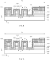
- FIG. 5 is a cross-sectional view taken along the B-B' direction in FIG. 2 , which shows a cross-sectional structure of the non-display area NA of the display substrate
- FIG. 6 is a cross-sectional view taken along the C-C' direction in FIG. 2 , which shows a cross-sectional structure of the display area AA of the display substrate.
- the display substrate may include: a metal layer 531, an interlayer dielectric layer 532, a conductive wire 533, a planarization layer 534, a conductive layer 535 and a cathode layer 536 which are disposed on a base substrate 50 and located in the non-display area NA.
- the metal layer 531, the interlayer dielectric layer 532, the conductive wire 533, the planarization layer 534, the conductive layer 535, and the cathode layer 536 are sequentially disposed on the base substrate 50.
- the display substrate includes a driving transistor DT and a switching transistor ST.
- Both the driving transistor DT and the switching transistor ST may be thin film transistors.
- the driving transistor DT may include: a first buffer layer 511, a first active layer 512, a first gate insulating layer 513, a first gate layer 514, a first interlayer dielectric layer 515, a first source-drain layer 516 and a first planarization layer 517 which are disposed on a base substrate 50 and located in the display area AA.
- the switching transistor ST may include a second buffer layer 541, a second active layer 542, a second gate insulating layer 543, a second gate layer 544, a second interlayer dielectric layer 545, a second source-drain layer 546, and a second planarization layer 547 which are disposed on the base substrate 50 and located in the display area AA.
- the first buffer layer 511 may be located in the same layer and made of the same material as the second buffer layer 541, that is, the first buffer layer 511 and the second buffer layer 541 are formed as the same film layer.
- the first interlayer dielectric layer 515 may be located in the same layer and made of the same material as the second interlayer dielectric layer 545, that is, the first interlayer dielectric layer 515 and the second interlayer dielectric layer 545 are formed as the same film layer.
- the first planarization layer 517 may be located in the same layer and made of the same material as the second planarization layer 547, that is, the first planarization layer 517 and the second planarization layer 547 are formed as the same film layer.
- the first gate insulating layer 513 may be located in the same layer and made of the same material as the second gate insulating layer 543, that is, the first gate insulating layer 513 and the second gate insulating layer 543 are formed as the same film layer.
- the first gate insulating layer 513 and the second gate insulating layer 543 are located in different layers, and they may be formed as different film layers.
- the display substrate further includes an organic light emitting device, a structure of which is similar to that of the organic light emitting device 22 shown in FIG. 4 .
- an organic light emitting device a structure of which is similar to that of the organic light emitting device 22 shown in FIG. 4 .
- the metal layer 531 may be located in the same layer and made of the same material as the second gate layer 544. It should be understood that the metal layer 531 in the non-display area NA is not electrically connected to the second gate layer 544 in the display area AA.
- the interlayer dielectric layer 532 may be located in the same layer and made of the same material as the interlayer dielectric layers 515, 545, that is, the interlayer dielectric layer 532 in the non-display area NA and the interlayer dielectric layers 515, 545 in the display area AA may be formed as the same film layer.
- the planarization layer 534 may be located in the same layer and made of the same material as the planarization layers 517, 547, that is, the planarization layer 534 in the non-display area NA and the planarization layers 517, 547 in the display area AA may be formed as the same film layer.
- the conductive wire 533 may be located in the same layer and made of the same material as the second source-drain layer 546.
- the conductive layer 535 may be located in the same layer and made of the same material as the anode of the organic light emitting device. It should be understood that the conductive layer is not electrically connected to the anode.
- the cathode layer 536 may be located in the same layer and made of the same material as the cathode of the organic light emitting device, and the cathode layer 536 located in the non-display area NA and the cathode located in the display area AA may be formed as the same film layer, that is, the cathode layer 536 in the display area NA is electrically connected to the cathode located in the display area AA.
- the display substrate further includes a plurality of trenches 537 formed in the interlayer dielectric layer 532. At least a part of the conductive wire 533 is formed in the trenches 537. As shown, the conductive wire 533 has a zigzag structure.
- the conductive wire 533 may include a first portion 533A extending in the first direction (such as the X direction), a second portion 533B extending in the second direction (such as the Y direction), and a third portion 533C extending in the first direction.
- the second portion 533B is located between the first portion 533A and the second portion 533C, and connects the first portion 533A with the second portion 533C.
- the first portion 533A is formed on a bottom of the trench 537
- the second portion 533B is formed on a sidewall of the trench 537
- the third portion 533C is formed on the interlayer dielectric layer 532.
- each trench 537 penetrates the interlayer dielectric layer 532 in the second direction, so that the first portion 533A of the conductive wire 533 is directly formed on the metal layer 531.
- the first portion 533A is directly formed on the metal layer 531
- the third portion 533C is directly formed on the interlayer dielectric layer 532.
- the first portion 533A and the third portion 533C are located at different height positions in the second direction, and the second portion 533B extending in the second direction connects the first portion 533A with the third portion 533C which is located at a different height position from the first portion 533A .
- a height difference between the first portion 533A and the third portion 533C in the second direction is substantially equal to a film thickness of the interlayer dielectric layer 532, that is, a height of the second portion 533B in the second direction is substantially equal to the film thickness of the interlayer dielectric layer 532.
- the conductive wire 533 includes a plurality of conductive wire sub-portions 533', which is indicated by a part of the conductive wire framed by a dotted line in the figure.
- Each conductive wire sub-portion 533' has a " " shape, and includes a first segment 5331 (i.e., a part of one first portion 533A), a second segment 5332 (i.e., one second portion 533B), a third segment 5333 (i.e., one third portion 533C), a fourth segment 5334 (i.e., another second portion 533B) and a fifth segment 5335 (i.e., a part of another first portion 533A) which are connected in sequence.
- the plurality of conductive wire sub-portions 533' are periodically arranged in the first direction to form the conductive wire 533.
- the conductive wire 533 includes a plurality of second portions extending in the second direction, which may further reduce the border width occupied by the conductive wire on one side of the frame, thereby realizing a narrow frame. Moreover, a reduced resistance voltage drop (IR Drop) and a good long-range uniformity (LRU) may be obtained.
- the conductive wire 533 is in direct electrical contact with the metal layer 531,so as to form a parallel connection. The resistance value of the conductive wire is further reduced, which may further reduce the resistance drop (IR Drop) and improve the long range uniformity (LRU).
- an orthographic projection of the conductive wire 533 on the base substrate 50 may have an inverted U-shape.
- a width w1 of the first portion 533A in the first direction may be equal to a width w3 of the third portion 533C in the first direction, and a height w2 of the second portion 533B in the second direction may be smaller than the width w1 of the first portion 533A in the first direction.
- the film thickness of the interlayer dielectric layer 532 may be 0.5 ⁇ m
- a width of each trench 537 in the first direction may be 6 ⁇ m
- an interval between two adjacent trenches 537 may be 6 ⁇ m, that is, the width w1 of the first portion 533A in the first direction may be 6 ⁇ m
- the height w2 of the second portion 533B in the second direction may be 0.5 ⁇ m
- the width w3 of the third portion 533C in the first direction may be 6 ⁇ m.
- the width of the conductive wire 533 in the first direction may be reduced by (0.5 / (6 + 0.5)), that is, reduced by 1/13.
- the border width occupied by the conductive wire 533 on one side of the frame may be reduced by 1/13.
- the border width occupied by the conductive wire on one side of the frame may be reduced by about 15.4 ⁇ m.
- FIG. 7 is a cross-sectional view taken along the B-B' direction in FIG. 2 , which shows a cross-sectional structure of the non-display area NA of the display substrate.
- the display substrate may include: a metal layer 731, a first insulating layer 738, an interlayer dielectric layer 732, a conductive wire 733, a planarization layer 734, a conductive layer 735 and a cathode layer 736 which are disposed on a base substrate 70 and located in the non-display area NA.
- the metal layer 731, the first insulating layer 738, the interlayer dielectric layer 732, the conductive wire 733, the planarization layer 734, the conductive layer 735, and the cathode layer 736 are sequentially disposed on the base substrate 70.
- the metal layer 731 may be located in the same layer and made of the same material as the first gate layer 514. It should be understood that the metal layer 731 in the non-display area NA is not electrically connected to the first gate layer 514 in the display area AA.
- the first insulating layer 738 may be located in the same layer and made of the same material as the first gate insulating layer 513, that is, the first insulating layer 738 in the non-display area NA and the first gate insulating layer 513 in the display area AA may be formed as the same film layer.
- the interlayer dielectric layer 732 may be located in the same layer and made of the same material as the interlayer dielectric layers 515, 545, that is, the interlayer dielectric layer 732 in the non-display area NA and the interlayer dielectric layers 515, 545 in the display area AA may be formed as the same film layer.
- the planarization layer 734 may be located in the same layer and made of the same material as the planarization layers 517, 547, that is, the planarization layer 734 in the non-display area NA and the planarization layers 517, 547 in the display area AA may be formed as the same film layer.
- the conductive wire 733 may be located in the same layer and made of the same material as the second source-drain layer 546.
- the conductive layer 735 may be located in the same layer and made of the same material as the anode of the organic light emitting device. It should be understood that the conductive layer is not electrically connected to the anode.
- the cathode layer 736 may be located in the same layer and made of the same material as the cathode of the organic light emitting device, and the cathode layer 736 located in the non-display area NA and the cathode located in the display area AA may be formed as the same film layer, that is, the cathode layer 736 located in the non-display area NA is electrically connected to the cathode located in the display area AA.
- the display substrate further includes a plurality of trenches 737 formed in the first insulating layer 738 and the interlayer dielectric layer 732.
- each trench 737 penetrates both the first insulating layer 738 and the interlayer dielectric layer 732 in the second direction.
- the conductive wire 733 is formed in the trenches 737 so that the conductive wire 733 may have a zigzag structure.
- the conductive wire 733 may include a first portion 733A extending in the first direction, a second portion 733B extending in the second direction, and a third portion 733C extending in the first direction.
- the second portion 733B is located between the first portion 733A and the third portion 733C, and connects the first portion 733A with the third portion 733C.
- the first portion 733A is formed on a bottom of the trench 737
- the second portion 733B is formed on a sidewall of the trench 737
- the third portion 733C is formed on the interlayer dielectric layer 732.
- the first portion 733A of the conductive wire 733 is directly formed on the metal layer 731.
- the first portion 733A is directly formed on the metal layer 731
- the third portion 733C is directly formed on the interlayer dielectric layer 732.
- the first portion 733A and the third portion 733C are located at different height positions in the second direction, and the second portion 733B extending in the second direction connects the first portion 733A with the third portion 733C which is located at a different height position from the first portion 733A.
- the conductive wire 733 includes a plurality of second portions 733B extending in the second direction. Since each trench 737 penetrates both the first insulating layer 738 and the interlayer dielectric layer 732, a height of the second portion 733B in the second direction is substantially equal to a sum of film thicknesses of the metal layer 731 and the interlayer dielectric layer 732. In this way, the border width occupied by the conductive wire on one side of the frame may be further reduced, which is more conducive to achieving a narrow frame. Moreover, a reduced resistance voltage drop (IR Drop) and a good long-range uniformity (LRU) may be obtained.
- IR Drop resistance voltage drop
- LRU long-range uniformity
- the conductive wire 733 is in direct electrical contact with the metal layer 731, so as to form a parallel connection.
- the resistance value of the conductive wire is further reduced, which may further reduce the resistance drop (IR Drop) and improve the long range uniformity (LRU).
- a width w1 of the first portion 733A in the first direction may be equal to a width w3 of the third portion 733C in the first direction, and a height w2 of the second portion 733B in the second direction may be smaller than the width w1 of the first portion 733A in the first direction.
- the film thickness of the first insulating layer 738 may be 0.1 ⁇ m
- the film thickness of the interlayer dielectric layer 732 may be 0.5 ⁇ m
- a width of each trench 737 in the first direction may be 6 ⁇ m
- an interval between two adjacent trenches 737 may be 6 ⁇ m, that is, the width w1 of the first portion 733A in the first direction may be 6 ⁇ m
- the height w2 of the second portion 733B in the second direction may be 0.6 ⁇ m
- the width w3 of the third portion 733C in the first direction may be 6 ⁇ m.
- the width of the conductive wire 733 in the first direction may be reduced by (0.6 / (6 + 0.6)), that is, reduced by 1/11. That is, the border width occupied by the conductive wire 733 on one side of the frame may be reduced by 1/11.
- the border width occupied by the conductive wire on one side of the frame may be reduced by about 18.2 ⁇ m.
- an orthographic projection of the conductive wire 733 on the base substrate 70 may have an inverted U-shape, and the conductive wire 733 also includes a plurality of conductive wire sub-portions arranged in a periodic manner, which can be referred to the above description, and will not be repeated here.
- FIG. 8 is a cross-sectional view taken along the B-B' direction in FIG. 2 , which shows a cross-sectional structure of the non-display area NA of the display substrate.
- the display substrate may include: a polysilicon layer 831, a first insulating layer 838, a second insulating layer 839, an interlayer dielectric layer 832, a conductive wire 833, a planarization layer 834, a conductive layer 835, and a cathode layer 836 which are disposed on a base substrate 80 and located in the non-display area NA.
- the polysilicon layer 831, the first insulating layer 838, the second insulating layer 839, the interlayer dielectric layer 832, the conductive wire 833, the planarization layer 834, the conductive layer 835, and the cathode layer 836 are sequentially disposed on the base substrate 80.
- the polysilicon layer 831 may be located in the same layer and made of the same material as the first active layer 512, that is, the polysilicon layer 831 located in the non-display area NA and the active layer 512 located in the display area AA may be formed as the same film layer.
- the first insulating layer 838 may be located in the same layer and made of the same material as the first gate insulating layer 513, that is, the first insulating layer 838 in the non-display area NA and the first gate insulating layer 513 in the display area AA may be formed as the same film layer.
- the second insulating layer 839 may be located in the same layer and made of the same material as the second gate insulating layer 543, that is, the second insulating layer 839 in the non-display area NA and the second gate insulating layer 543 in the display area AA may be formed as the same film layer.
- the interlayer dielectric layer 832 may be located in the same layer and made of the same material as the interlayer dielectric layers 515, 545, that is, the interlayer dielectric layer 832 located in the non-display area NA and the interlayer dielectric layers 515, 545 located in the display area AA may be formed as the same film layer.
- the planarization layer 834 may be located in the same layer and made of the same material as the planarization layers 517, 547, that is, the planarization layer 834 in the non-display area NA and the planarization layers 517, 547 in the display area AA may be formed as the same film layer.
- the conductive wire 833 may be located in the same layer and made of the same material as the second source-drain layer 546.
- the conductive layer 835 may be located in the same layer and made of the same material as the anode of the organic light emitting device. It should be understood that the conductive layer is not electrically connected to the anode.
- the cathode layer 836 may be located in the same layer and made of the same material as the cathode layer of the organic light emitting device, and the cathode layer 836 located in the non-display area NA and the cathode located in the display area AA may be formed as the same film layer, that is, the cathode layer 836 located in the non-display area NA is electrically connected to the cathode located in the display area AA.
- the display substrate further includes a plurality of trenches 837 formed in the first insulating layer 838, the second insulating layer 839, and the interlayer dielectric layer 832.
- each trench 837 penetrates the first insulating layer 838, the second insulating layer 839, and the interlayer dielectric layer 832 in the second direction.
- the conductive wire 833 is formed in the trenches 837 so that the conductive wire 833 may have a zigzag structure.
- the conductive wire 833 may include a first portion 833A extending in the first direction, a second portion 833B extending in the second direction, and a third portion 833C extending in the first direction.
- the second portion 833B is located between the first portion 833A and the third portion 833C, and connects the first portion 833A with the third portion 833C.
- the first portion 833A is formed on a bottom of the trench 837
- the second portion 833B is formed on a sidewall of the trench 837
- the third portion 833C is formed on the interlayer dielectric layer 832.
- the first portion 833A of the conductive wire 833 is directly formed on the polysilicon layer 831.
- the first portion 833A is directly formed on the polysilicon layer 831
- the third portion 833C is directly formed on the interlayer dielectric layer 832.
- the first portion 833A and the third portion 833C are located at different height positions in the second direction, and the second portion 833B extending in the second direction connects the first portion 833A with the third portion 833C which is located at a different height position from the first portion 833A.
- the conductive wire 833 includes a plurality of second portions 833B extending in the second direction. Since each trench 837 penetrates the first insulating layer 838, the second insulating layer 839 and the interlayer dielectric layer 832, a height of the second portion 833B in the second direction is substantially equal to a sum of film thicknesses of the first insulating layer 838, the second insulating layer 839, and the interlayer dielectric layer 832. In this way, the border width occupied by the conductive wire on one side of the frame may be further reduced, which is more conducive to achieving a narrow frame. Meanwhile, a reduced resistance voltage drop (IR Drop) and a good long-range uniformity (LRU) may be obtained.
- IR Drop resistance voltage drop
- LRU long-range uniformity
- a width w1 of the first portion 833A in the first direction may be equal to a width w3 of the third portion 833C in the first direction, and a height w2 of the second portion 833B in the second direction may be smaller than the width w1 of the first portion 833A in the first direction.
- the film thickness of the first insulating layer 838 may be 0.1 ⁇ m
- the film thickness of the second insulating layer 838 may be 0.1 ⁇ m
- the film thickness of the interlayer dielectric layer 832 may be 0.5 ⁇ m
- a width of each trench 737 in the first direction may be 6 ⁇ m
- an interval between two adjacent trenches 737 may be 6 ⁇ m, that is, the width w1 of the first portion 833A in the first direction may be 6 ⁇ m
- the height w2 of the second portion 833A in the second direction may be 0.7 ⁇ m
- the width w3 of the third portion 833C in the first direction may be 6 ⁇ m.
- the width of the conductive wire 833 in the first direction may be reduced by (0.7 / (6 + 0.7)), that is, reduced by 1/10. That is, the border width occupied by the conductive wire 833 on one side of the frame can be reduced by 1/10.
- the border width occupied by the conductive wire on one side of the frame can be reduced by about 20 ⁇ m.
- an orthographic projection of the conductive wire 833 on the base substrate 80 may have an inverted U-shape, and the conductive wire 833 also includes a plurality of conductive wire sub-portions arranged in a periodic manner, which can be referred to the above description and will not be repeated here.
- FIG. 9 is a cross-sectional view taken along the B-B' direction in FIG. 2 , which shows a cross-sectional structure of the non-display area NA of the display substrate.
- the display substrate may include: a buffer layer 931, a first insulating layer 938, a second insulating layer 939, an interlayer dielectric layer 932, a conductive wire 933, a planarization layer 934, a conductive layer 935, and a cathode layer 936 which are disposed on a base substrate 90 and located in the non-display area NA.
- the buffer layer 931, the first insulating layer 938, the second insulating layer 939, the interlayer dielectric layer 932, the conductive wire 933, the planarization layer 934, the conductive layer 935, and the cathode layer 936 are sequentially disposed on the base substrate 90.
- the buffer layer 931 may be located in the same layer and made of the same material as the first buffer layer 511, that is, the buffer layer 931 in the non-display area NA and the first buffer layer 511 in the display area AA may be formed as the same film layer.
- the first insulating layer 938 may be located in the same layer and made of the same material as the first gate insulating layer 513, that is, the first insulating layer 938 in the non-display area NA and the first gate insulating layer 513 in the display area AA may be formed as the same film layer.
- the second insulating layer 939 may be located in the same layer and made of the same material as the second gate insulating layer 543, that is, the first insulating layer 939 in the non-display area NA and the second gate insulating layer 543 in the display area AA may be formed as the same film layer.
- the interlayer dielectric layer 932 may be located in the same layer and made of the same material as the interlayer dielectric layers 515, 545, that is, the interlayer dielectric layer 932 located in the non-display area NA and the interlayer dielectric layers 515, 545 located in the display area AA may be formed as the same film layer.
- the planarization layer 934 may be located in the same layer and made of the same material as the planarization layers 517, 547, that is, the planarization layer 934 in the non-display area NA and the planarization layers 517, 547 in the display area AA may be formed as the same film layer.
- the conductive wire 933 may be located in the same layer and made of the same material as the second source-drain layer 546.
- the conductive layer 935 may be located in the same layer and made of the same material as the anode of the organic light emitting device. It should be understood that the conductive layer is not electrically connected to the anode.
- the cathode layer 936 may be located in the same layer and made of the same material as the cathode of the organic light emitting device, and the cathode layer 936 located in the non-display area NA and the cathode located in the display area AA may be formed as the same film layer, that is, the cathode layer 936 located in the display area NA is electrically connected to the cathode located in the display area AA.
- the display substrate further includes a plurality of trenches 937 formed in the buffer layer 931, the first insulating layer 938, the second insulating layer 939, and the interlayer dielectric layer 932.
- each trench 937 penetrates the buffer layer 931, the first insulating layer 938, the second insulating layer 939 and the interlayer dielectric layer 932 in the second direction.
- the conductive wire 933 is formed in the trenches 937 so that the conductive wire 933 may have a zigzag structure.
- the conductive wire 933 may include a first portion 933A extending in the first direction, a second portion 933B extending in the second direction, and a third portion 933C extending in the first direction.
- the second portion 933B is located between the first portion 933A and the third portion 933C, and connects the first portion 933A with the third portion 933C.
- the first portion 933A is formed on a bottom of the trench 937
- the second portion 933B is formed on a sidewall of the trench 937
- the third portion 933C is formed on the interlayer dielectric layer 932.
- the first portion 933A of the conductive wire 933 is formed directly on the base substrate 90.
- the first portion 933A is directly formed on the base substrate 90
- the third portion 933C is directly formed on the interlayer dielectric layer 932.
- the first portion 933A and the third portion 933C are located at different height positions in the second direction, and the second portion 933B extending in the second direction connects the first portion 933A with the third portion 933C which is located at a different height position from the first portion 933A.
- the conductive wire 933 includes a plurality of second portions 933B extending in the second direction. Since each trench 937 penetrates the buffer layer 931, the first insulating layer 938, the second insulating layer 939, and the interlayer dielectric layer 932, a height of the second portion 933B in the second direction is substantially equal to a sum of film thicknesses of the buffer layer 931, the first insulating layer 938, the second insulating layer 939, and the interlayer dielectric layer 932. In this way, the border width occupied by the conductive wire on one side of the frame may be further reduced, which is more conducive to achieving a narrow frame. Meanwhile, a reduced resistance voltage drop (IR Drop) and a good long-range uniformity (LRU) may be obtained.
- IR Drop resistance voltage drop
- LRU long-range uniformity
- a width w1 of the first portion 933A in the first direction may be equal to a width w3 of the third portion 933C in the first direction, and a height w2 of the second portion 933B in the second direction may be smaller than the width w1 of the first portion 933A in the first direction.
- the film thickness of the buffer layer 931 may be 0.4 ⁇ m
- the film thickness of the first insulating layer 938 may be 0.1 ⁇ m
- the film thickness of the second insulating layer 938 may be 0.1 ⁇ m
- the film thickness of the interlayer dielectric layer 932 may be 0.5 ⁇ m
- a width of each trench 937 in the first direction may be 6 ⁇ m
- an interval between two adjacent trenches 937 may be 6 ⁇ m, that is, the width w1 of the first portion 933A in the first direction may be 6 ⁇ m
- the height w2 of the second portion 933B in the second direction may be 1.1 ⁇ m
- the width w3 of the third portion 933C in the first direction may be 6 ⁇ m.
- the width of the conductive wire 933 in the first direction may be reduced by (1.1 / (6 + 1.1)), that is, reduced by 1/6. That is, the border width occupied by the conductive wire 933 on one side of the frame may be reduced by 1/6.
- the border width occupied by the conductive wire on one side of the frame may be reduced by about 33 ⁇ m.
- an orthographic projection of the conductive wire 933 on the base substrate 90 may have an inverted U-shape, and the conductive wire 933 also includes a plurality of conductive wire sub-portions arranged in a periodic manner, which can be referred to the above description and will not be repeated here.
- FIG. 10 is a cross-sectional view taken along the B-B' direction in FIG. 2 , which shows a cross-sectional structure of the non-display area NA of the display substrate.
- the display substrate may include a barrier layer 1040, a buffer layer 1031, a first insulating layer 1038, a second insulating layer 1039, an interlayer dielectric layer1032, a conductive wire 1033, a planarization layer 1034, a conductive layer 1035, and a cathode layer 1036 which are disposed on a base substrate 100 and located in the non-display area NA.
- the barrier layer 1040, the buffer layer 1031, the first insulating layer 1038, the second insulating layer 1039, the interlayer dielectric layer 1032, the conductive wire 1033, the planarization layer 1034, the conductive layer 1035, and the cathode layer 1036 are sequentially disposed on the substrate 90.
- a barrier layer is also provided on the base substrate 100.
- a barrier layer is provided between the base substrate 50 and the first buffer layer 511.
- the barrier layer 1040 located in the non-display area NA and the barrier layer located in the display area AA may be formed as the same film layer.
- the structures of other film layers such as the buffer layer 1031, the first insulating layer 1038, the second insulating layer 1039, the interlayer dielectric layer 1032, the conductive wire 1033, the planarization layer 1034, the conductive layer 1035, and the cathode layer 1036 may be referred to the above description of FIG.9 , which will not be repeated here.
- the display substrate further includes a plurality of trenches 1037 formed in the barrier layer 1040, the buffer layer 1031, the first insulating layer 1038, the second insulating layer 1039, and the interlayer dielectric layer 1032.
- each trench 1037 penetrates the barrier layer 1040, the buffer layer 1031, the first insulating layer 1038, the second insulating layer 1039, and the interlayer dielectric layer 1032 in the second direction.
- the conductive wire 1033 is formed in the trenches 1037, so that the conductive wire 1033 may have a zigzag structure.
- the conductive wire 1033 may include a first portion 1033A extending in the first direction, a second portion 1033B extending in the second direction, and a third portion 1033C extending in the first direction.
- the second portion 1033B is located between the first portion 1033A and the third portion 1033C, and connects the first portion 1033A with the third portion 1033C.
- the first portion 1033A is formed on a bottom of the trench 1037
- the second portion 1033B is formed on a sidewall of the trench 1037
- the third portion 1033C is formed on the interlayer dielectric layer 1032.
- the first portion 1033A of the conductive wire 1033 is directly formed on the base substrate 100.
- the first portion 1033A is directly formed on the base substrate 100
- the third portion 1033C is directly formed on the interlayer dielectric layer 1032.
- the first portion 1033A and the third portion 1033C are located at different height positions in the second direction, and the second portion 1033B extending in the second direction connects the first portion 1033A with the third portion 1033C which is located at a different height position from the first portion 1033A.
- the conductive wire 1033 includes a plurality of second portions 1033B extending in the second direction. Since each trench 1037 penetrates the barrier layer 1040, the buffer layer 1031, the first insulating layer 1038, the second insulating layer 1039, and the interlayer dielectric layer 1032, a height of the second portion 1033B in the second direction is substantially equal to a sum of film thicknesses of the barrier layer 1040, the buffer layer 1031, the first insulating layer 1038, the second insulating layer 1039, and the interlayer dielectric layer 1032. In this way, the border width occupied by the conductive wire on one side of the frame may be further reduced, which is more conducive to achieving a narrow frame. Meanwhile, a reduced resistance voltage drop (IR Drop) and a good long-range uniformity (LRU) may be obtained
- a width w1 of the first portion 1033A in the first direction may be equal to a width w3 of the third portion 1033C in the first direction, and a height w2 of the second portion 1033B in the second direction may be smaller than the width w1 of the first portion 1033A in the first direction.
- the film thickness of the barrier layer 1040 may be 0.4 ⁇ m
- the film thickness of the buffer layer 1031 may be 0.4 ⁇ m
- the film thickness of the first insulating layer 1038 may be 0.1 ⁇ m
- the film thickness of the second insulating layer 1038 may be 0.1 ⁇ m
- the film thickness of the interlayer dielectric layer 1032 may be 0.5 ⁇ m
- a width of each trench 1037 in the first direction may be 6 ⁇ m
- an interval between two adjacent trenches 1037 may be 6 ⁇ m, that is, the width withe first portion 1033A in the first direction may be 6 ⁇ m
- the height w2 of the second portion 1033B in the second direction may be 1.5 ⁇ m
- the width w3 of the third portion 1033C in the first direction may be 6 ⁇ m.
- the width of the conductive wire 1033 in the first direction may be reduced by (1.5 / (6 + 1.5)), that is, reduced by 1/5. That is, the border width occupied by the conductive wire 1033 on one side of the frame may be reduced by 1/5.
- the border width occupied by the conductive wire on one side of the frame may be reduced by about 40 ⁇ m.
- an orthographic projection of the conductive wire 1033 on the base substrate 100 may have an inverted U-shape, and the conductive wire 1033 also includes a plurality of conductive wire sub-portions arranged in a periodic manner, which can be referred to the above description and will not be repeated here.
- FIG. 11 is a cross-sectional view taken along the B-B' direction in FIG. 2 , which shows a cross-sectional structure of the non-display area NA of the display substrate.
- the structure of the display substrate in the non-display area NA shown in FIG. 11 is similar to that of the display substrate in the non-display area NA shown in FIG. 5 . Differences between the two structures are mainly explained hereinafter.
- the conductive wire 1133 may include a first portion 1133A extending in the first direction, a second portion 1133B extending in the second direction, and a third portion 1133C extending in the first direction.
- the second portion 1133B is located between the first portion 1133A and the second portion 1133C, and connects the first portion 1133A with the second portion 1133C.
- the first portion 1133A is formed on the bottom of the trench
- the second portion 1133B is formed on the sidewall of the trench
- the third portion 1133C is formed on the interlayer dielectric layer.
- a width w1 of the first portion 1133A in the first direction may be equal to a width w3 of the third portion 1133C in the first direction, and a height w2 of the second portion 1133B in the second direction may be smaller than the width w1 of the first portion 1133A in the first direction.
- a width of an orthographic projection of the conductive wire 1133, which is on one side of the frame, on the base substrate in the first direction may be at least equal to a width of an orthographic projection of the conductive wire 14 on the base substrate in the first direction in the embodiments shown in FIG. 1B . That is, the two conductive wires occupy the same border width.
- the width of the orthographic projection of the conductive wire 1133, which is on one side of the frame, on the base substrate in the first direction is 200 ⁇ m or more.
- the overall width of the conductive wire 1133 is equal to the sum of the widths w1 of the first portions 1133A in the first direction, the heights w2 of the second portions 1133B in the second direction and the widths w3 of the third portions 1133C in the first direction, the overall width of the conductive wire 1133 is larger than the overall width of the conductive wire 14. Therefore, the conductive wire 1133 has a smaller resistance value. In this way, when the size of the frame is unchanged, by forming a conductive wire having a zigzag shape, the resistance value of the conductive wire may be reduced, thereby reducing the resistance voltage drop and further improving the long range uniformity.
- the embodiments of the present disclosure have been described by taking the OLED display substrate as an example of the display substrate.
- the display substrate according to the embodiments of the present disclosure may also be other types of display substrates.
- the display substrate may be an LCD substrate.
- the above-mentioned conductive wires may be a common electrode conductive wire, for example, the conductive wires 533, 733, 833, 933, 1033 and 1133 may be common electrode conductive wires, which are used to electrically connect a common electrode of the LCD substrate with an integrated circuit IC, and the common electrode may be located in a display area of the LCD substrate.
- the specific structure of the common electrode conductive wire may be similar to the structures described above and is not repeated here.
- FIG. 5 a method of manufacturing a display substrate according to some embodiments of the present disclosure will be described with reference to FIGS. 12A-12F and FIG. 13 .
- a base substrate 50 is provided, and a metal material layer 531' is formed on the base substrate 50, as shown in FIG. 12A .
- the metal material layer 531' is formed in both a display area AA and a non-display area NA of the base substrate 50, and a part of the metal material layer 531' in the non-display area NA constitutes a metal layer 531.
- an interlayer insulating material layer 532' is formed on the metal material layer 531', as shown in FIG. 12B .
- the interlayer insulating material layer 532' is formed in both the display area AA and the non-display area NA of the base substrate 50, and a part of the interlayer insulating material layer 532' in the non-display area NA constitutes an interlayer insulating layer 532.
- a plurality of trenches 537 are formed in the interlayer insulating material layer 532'.
- the plurality of trenches 537 may be formed in the interlayer insulating material layer 532' located in the non-display area NA through a patterning process, as shown in FIG. 12C .
- a source-drain material layer 546' is formed on the interlayer insulating material layer 532' and in the trenches 537, as shown in FIG. 12D .
- the source-drain material layer 546' is formed on the interlayer insulating material layer 532' and in the trenches 537 by a process such as deposition.
- the source-drain material layer 546' is formed in both the display area AA and the non-display area NA.
- step S134 a patterning process is performed on the source-drain material layer 546' so that a part of the source-drain material layer 546' located in the non-display area NA is formed as a conductive wire 533, as shown in FIG. 12E .
- the part of the source-drain layer 546' located in the non-display area NA is formed as the conductive wire 533 (see FIG. 12E and FIG. 5 ), and a part of the source-drain material layer 546' in the display area AA is formed as a second source-drain layer 546 (see FIG. 6 ).
- step S135 a planarization material layer 534' is formed on the conductive wire 533, the interlayer insulating material layer 532', and the second source-drain layer 546, as shown in FIG. 12F .
- step S136 a patterning process is performed on the planarization material layer 534' to remove a part of the planarization material layer 534' over the conductive wire 533, as shown in FIG. 12G .
- step S137 an anode material layer 535' is formed on a part, on which the planarization material layer has been removed, of the conductive wire 533 and on the planarization material layer, as shown in FIG. 12H .
- step S138 a patterning process is performed on the anode material layer 535', so that a part of the anode material layer 535' located in the non-display area NA is formed as a conductive layer 535, as shown in FIG. 12I .
- a part of the anode material layer 535' located in the non-display area NA is formed as a conductive layer 535 (see FIG. 12I and FIG.5 ), and a part of the anode material layer 535' located in the display area AA is formed as an anode of an organic light emitting device.
- a cathode layer 536 is formed on the conductive layer 535, as shown in FIG.5 .
- a cathode material layer may be formed in both the non-display area NA and the display area AA by a vapor deposition process, in particular, by one vapor deposition process.
- a patterning process may be performed on the cathode material layer, so that a part of the cathode material layer located in the non-display area NA is formed as the cathode layer 536 (see FIG. 5 ).
- a display substrate having a conductive wire as shown in FIG. 5 may be formed, so that the border width occupied by the conductive wire on one side of the frame may be reduced, which is conducive to achieving a narrow frame. Meanwhile, a reduced resistance voltage drop (IR Drop) and a good long-range uniformity (LRU) may be obtained.
- each layer in the multilayer structure located in the non-display area is basically formed by the same patterning process as a corresponding layer located in the display area, thus, no additional patterning process is added, which is conducive to process realization and may save manufacturing costs.
- FIG. 14 shows a plan view of a display device according to some embodiments of the present disclosure.
- the display device 1400 may include the display substrate described in any one of the above.
- the display device may be any product or member with a display function, such as a smart phone, a wearable smart watch, smart glasses, a tablet computer, a television, a display, a notebook computer, a digital photo frame, a navigator, a car display, an e-book, etc.
- a display device according to some embodiments of the present disclosure may implement a narrow frame.
Landscapes
- Engineering & Computer Science (AREA)
- Microelectronics & Electronic Packaging (AREA)
- Manufacturing & Machinery (AREA)
- Electroluminescent Light Sources (AREA)
- Devices For Indicating Variable Information By Combining Individual Elements (AREA)
Abstract
Description
- The present disclosure relates to the field of display technology, and in particular, to a display substrate, a method of manufacturing the same, and a display device.
- Existing organic light emitting devices include an active matrix (abbreviated as AM) manner or a passive matrix (abbreviated as PM) manner. In these two types of organic light emitting display devices, there are strict requirements for a resistance value of a conductive wire. In order to make the resistance value of the conductive wire small, a wide conductive wire is usually used. However, the conductive wire is generally arranged in a non-display area of a display screen. An excessively wide conductive wire will increase an area of the non-display area, which is not conducive to the realization of a display device with a narrow frame.
- Some embodiments of the present disclosure provide a display substrate comprising: a base substrate comprising a peripheral area; and a conductive wire disposed on the base substrate and located in the peripheral area, wherein the conductive wire comprises: a first portion extending in a first direction parallel to an upper surface of the base substrate; and a second portion extending in a second direction perpendicular to the upper surface of the base substrate.
- In some embodiments, the wire comprises at least two second portions.
- In some embodiments, the conductive wire further comprises a third portion extending in the first direction, and the second portion connects the first portion with the third portion.
- In some embodiments, the conductive wire comprises at least one conductive wire sub-portion, and each conductive wire sub-portion comprises a first segment, a second segment, a third segment, a fourth segment and a fifth segment connected in sequence; and wherein the first segment and fifth segment constitute the first portion, the second segment and the fourth segment constitute the second portion, and the third segment constitutes the third portion.
- In some embodiments, the conductive wire comprises a plurality of conductive wire sub-portions, and the plurality of conductive wire sub-portions are periodically arranged.
- In some embodiments, the display substrate further comprising: an interlayer dielectric layer disposed on the base substrate and located in the peripheral area; and a trench in the interlayer dielectric layer, wherein the first portion is located on a bottom of the trench, the second portion is located on a sidewall of the trench, and the third portion is located on the interlayer dielectric layer.
- In some embodiments, the trench penetrates the interlayer dielectric layer in the second direction.
- In some embodiments, the display substrate further comprising: a first insulating layer disposed on the base substrate and located in the peripheral area; an interlayer dielectric layer disposed on the first insulating layer and located in the peripheral area; and a trench formed in both the first insulating layer and the interlayer dielectric layer, wherein the first portion is located on a bottom of the trench, the second portion is located on a sidewall of the trench, and the third portion is located on the interlayer dielectric layer.
- In some embodiments, the trench penetrates both the first insulating layer and the interlayer dielectric layer in the second direction.
- In some embodiments, the display substrate further comprising: a first insulating layer disposed on the base substrate and located in the peripheral area; a second insulating layer disposed on the first insulating layer and located in the peripheral area; an interlayer dielectric layer disposed on the second insulating layer and located in the peripheral area; and a trench formed in all of the first insulating layer, the second insulating layer, and the interlayer dielectric layer, wherein the first portion is located on a bottom of the trench, the second portion is located on a sidewall of the trench, and the third portion is located on the interlayer dielectric layer.
- In some embodiments, the trench penetrates all of the first insulating layer, the second insulating layer and the interlayer dielectric layer in the second direction.
- In some embodiments, the display substrate further comprising: a buffer layer disposed on the base substrate and located in the peripheral area; a first insulating layer disposed on the buffer layer and located in the peripheral area; a second insulating layer disposed on the first insulating layer and located in the peripheral area; an interlayer dielectric layer disposed on the second insulating layer and located in the peripheral area; and a trench formed in all of the buffer layer, the first insulating layer, the second insulating layer and the interlayer dielectric layer, wherein the first portion is located on a bottom of the trench, the second portion is located on a sidewall of the trench, and the third portion is located on the interlayer dielectric layer.
- In some embodiments, the trench penetrates all of the buffer layer, the first insulating layer, the second insulating layer, and the interlayer dielectric layer in the second direction.
- In some embodiments, the display substrate further comprising: a barrier layer disposed on the base substrate and located in the peripheral area; a buffer layer disposed on the barrier layer and located in the peripheral area; a first insulating layer disposed on the buffer layer and located in the peripheral area; a second insulating layer disposed on the first insulating layer and located in the peripheral area; an interlayer dielectric layer disposed on the second insulating layer and located in the peripheral area; and a trench formed in all of the barrier layer, the buffer layer, the first insulating layer, the second insulating layer and the interlayer dielectric layer, wherein the first portion is located on a bottom of the trench, the second portion is located on a sidewall of the trench, and the third portion is located on the interlayer dielectric layer.
- In some embodiments, wherein the trench penetrates all of the barrier layer, the buffer layer, the first insulating layer, the second insulating layer, and the interlayer dielectric layer.
- In some embodiments, the number of the trench is at least two.
- In some embodiments, a ratio of a height of the second portion in the second direction to a sum of a width of the first portion in the first direction and the height of the second portion in the second direction is greater than or equal to 1/13.
In some embodiments, the base substrate further comprises a middle area, the peripheral area surrounding the middle area, the display substrate further comprises: a thin film transistor disposed on the base substrate and located in the middle area, the thin film transistor comprising a source-drain layer, wherein the conductive wire and the source-drain layer are located in the same layer and formed of the same material. - In some embodiments, the display substrate further comprising: an organic light emitting device disposed on the base substrate and located in the middle area, the organic light emitting device comprising an anode, a cathode, and a light emitting layer between the anode and the cathode; and a conductive layer disposed on the conductive wire and located in the peripheral area, wherein the conductive layer electrically connects the cathode with the conductive wire.
- In some embodiments, the conductive layer and the anode are located in the same layer and formed of the same material.
- In some embodiments, the display substrate further comprising a common electrode disposed on the base substrate and located in the middle area, wherein the conductive wire is electrically connected to the common electrode.
- Some embodiments of the present disclosure provide a display device comprising the display substrate according to the above embodiments.
- Some embodiments of the present disclosure provide a method of manufacturing a display substrate, comprising the following steps: providing a base substrate comprising a peripheral area; forming an insulating layer in the peripheral area; forming at least one trench in the insulating layer; and forming a conductive wire in the trench and on the insulating layer, so that the conductive wire comprises: a first portion located on a bottom of the trench; and a second portion located on a sidewall of the trench.
- Other objects and advantages of the present disclosure will be apparent from the following description of the present disclosure with reference to the accompanying drawings, which may help to have a comprehensive understanding of the present disclosure.
-
FIG. 1A is a plan view of a display substrate in the related art; -
FIG. 1B is a cross-sectional view taken along a B-B' direction inFIG. 1A ; -
FIG. 2 is a plan view of a display substrate according to some embodiments of the present disclosure; -
FIG. 3 is a cross-sectional view taken along a B-B' direction inFIG. 2 , which shows a cross-sectional structure in a non-display area on one side of the display substrate; -
FIG. 4 is a cross-sectional view taken along a C-C' direction inFIG. 2 , which shows a partial cross-sectional structure in a display area of the display substrate; -
FIG. 5 is a cross-sectional view taken along a B-B' direction inFIG. 2 , which shows a cross-sectional structure in a non-display area on one side of the display substrate, and specifically shows a conductive wire in a trench formed in an insulating layer; -
FIG. 6 is a cross-sectional view taken along a C-C' direction inFIG. 2 , which illustrates a partial cross-sectional structure in a display area of the display substrate; -
FIG. 7 is a cross-sectional view taken along a B-B' direction inFIG. 2 , which shows a cross-sectional structure in a non-display area on one side of the display substrate, and specifically shows a conductive wire in a trench formed in a first gate insulating layer and an interlayer dielectric layer; -
FIG. 8 is a cross-sectional view taken along a B-B' direction inFIG. 2 , which shows a cross-sectional structure in a non-display area on one side of the display substrate, and specifically shows a conductive wire in a trench formed in a first gate insulating layer, a second gate insulating layer and an interlayer dielectric layer; -
FIG. 9 is a cross-sectional view taken along a B-B' direction inFIG. 2 , which shows a cross-sectional structure in a non-display area on one side of the display substrate, and specifically shows a conductive wire in a trench formed in a buffer layer, a first gate insulating layer, a second gate insulating layer and an interlayer dielectric layer; -
FIG. 10 is a cross-sectional view taken along a B-B' direction inFIG. 2 , which shows a cross-sectional structure in a non-display area located on one side of the display substrate, and specifically illustrates a conductive wire in a trench formed in a barrier layer, a buffer layer, and a first gate insulating layer, a second gate insulating layer, and an interlayer dielectric layer; -
FIG. 11 is a cross-sectional view taken along a B-B' direction inFIG. 2 , which shows a cross-sectional structure in a non-display area located on one side of the display substrate; -
FIGS. 12A-12I schematically shows cross-sectional structures of a display substrate formed after each step of a method of manufacturing the display substrate according to some embodiments of the present disclosure is performed; -
FIG. 13 is a flowchart of a method of manufacturing a display substrate according to some embodiments of the present disclosure; and -
FIG. 14 is a plan view of a display device according to some embodiments of the present disclosure. - It should be noted that, for the sake of clarity, the dimensions of layers, structures or regions may be enlarged or reduced in the drawings for describing the embodiments of the present disclosure, that is, these drawings are not drawn to actual scale.
- The technical solutions of the present disclosure will be further described in detail through embodiments and the accompanying drawings. In the description, the same or similar reference numerals indicate the same or similar components. The following description of the embodiments of the present disclosure with reference to the drawings is intended to explain the general inventive concept of the present disclosure, and should not be construed as a limitation to the present disclosure.
- In addition, in the following detail description, for ease of explanation, many specific details are set forth to provide a comprehensive understanding of the embodiments of the present disclosure. Obviously, however, one or more embodiments may be implemented without these specific details.
- It should be noted that the terms "on", "formed on" and disposed on" cited in this article may mean that one layer is directly formed or disposed on another layer, or may mean that one layer is indirectly formed or disposed on another layer, that is, there are other layers between the two layers.
- It should be noted that, although the terms "first", "second" and the like may be used herein to describe various components, members, elements, regions, layers, and/or portions, these components, members, elements, regions, layers, and/or portions should not be limited by these terms. These terms are used to distinguish one component, member, element, region, layer, and/or portion from another. Thus, for example, a first component, a first member, a first element, a first region, a first layer, and/or a first portion discussed below may be referred to as a second component, a second member, a second element, a second region, a second layer, and/or second portion without departing from the teachings of the present disclosure.
- Herein, various layers of the display substrate such as a barrier layer, a buffer layer, a first insulating layer, a second insulating layer, an interlayer dielectric layer, and an insulating layer are described. Those skilled in the art should understand that these layers are generally formed of an insulating material, thus, without special distinction, the expression "insulating layer" may be used as their common name, that is, the expression "insulating layer" may include at least one of the barrier layer, the buffer layer, the first insulating layer, the second insulating layer and the interlayer dielectric layers. For example, the expression "insulating layer" may include the interlayer dielectric layer; or the expression "insulating layer" may include two layers of the interlayer dielectric layer and one of the first insulating layer and a second insulating layer; or the expression "insulating layer" may include three layers of the first insulating layer, the second insulating layer, and the interlayer dielectric layer; or the expression "insulating layer" may include four layers of the buffer layer, the first insulating layer, and the second insulating layer and the interlayer dielectric layer; or the expression "insulating layer" may include five layers of the barrier layer, the buffer layer, the first insulating layer, the second insulating layer, and the interlayer dielectric layer.
- As shown in
FIGS. 1A and 1B , a display substrate in the related art is shown, and in particular, a conductive wire of the display substrate in the related art is shown.FIG. 1A is a plan view of the display substrate, andFIG. 1B is a cross-sectional view taken along a B-B' direction inFIG. 1A . As shown inFIG. 1A , the display substrate includes abase substrate 10 including a middle area AA and a peripheral area NA surrounding the middle area AA. It can be understood that the middle area AA corresponds to a display area, which is used for displaying image, of a display device including the display substrate, and the peripheral area corresponds to a non-display area of the display device. For convenience of description, in this text, the middle area AA is referred to as a display area AA of thebase substrate 10 and/or the display substrate, and the peripheral area is referred to as a non-display area NA of thebase substrate 10 and/or the display substrate. As shown inFIG. 1B , the display substrate further includes: an insulatinglayer 12 disposed on thebase substrate 10 and located at least in the non-display area NA; and aconductive wire 14 disposed on the insulatinglayer 12 and located in the non-display area NA. There may be other layers between the insulatinglayer 12 and thebase substrate 10, for example, the insulatinglayer 12 may be an interlayer dielectric layer. - It should be noted that, in order to highlight the conductive wire, other structures or other layers are omitted in the plan view. For example, in
FIG. 1A , the insulatinglayer 12 is omitted. - As shown in
FIG. 1B , theconductive wire 14 are completely laid on the insulatinglayer 12. In order to make the resistance value of theconductive wire 14 small, it is generally necessary to set a width of theconductive wire 14, (i.e., a width w indicated in the figure) to be large. For example, taking the display substrate as an OLED display substrate as an example, theconductive wire 14 may be a cathode conductive wire (i.e., a VSS conductive wire), and the width w of theconductive wire 14 is generally 200 µm or more. However, the wideconductive wire 14 needs to occupy a large space in the non-display area, which is not conducive to the realization of a display device with a narrow frame. - Based on this, some embodiments of the present disclosure provide a display substrate. As shown in
FIG. 2 , a plan view of a display substrate according to some embodiments of the present disclosure is shown. The display substrate includes abase substrate 20 including a display area AA and a non-display area NA surrounding the display area AA. - In the following, an OLED display device is taken as an example to describe the display substrate according to some embodiments of the present disclosure. However, those skilled in the art should understand that the embodiments of the present disclosure are not limited to the OLED display device.
- It should be understood that the display substrate includes: a plurality of organic light emitting devices located in the display area AA; and a conductive wire located in the non-display area NA. The organic light emitting devices and the conductive wire will be described in more detail below with reference to the drawings. The display substrate further includes: an electrical connection portion (pad) 30 located in the non-display area NA. The
electrical connection portion 30 may be electrically connected to an integrated circuit IC, and the conductive wire is used to electrically connect an electrode (such as a cathode) of the organic light emitting device to theelectrical connection portion 30, and then to the integrated circuit IC. - In some embodiments,
FIG. 3 is a cross-sectional view taken along the B-B' direction inFIG. 2 , which shows a cross-sectional structure of the non-display area NA of the display substrate;FIG. 4 is a cross-sectional view taken along the C-C' direction inFIG. 2 , which shows a cross-sectional structure of the display area AA of the display substrate. - Optionally, as shown in
FIG. 4 , the display substrate includes athin film transistor 21. Specifically, thethin film transistor 21 may include: abuffer layer 211, anactive layer 212, agate insulating layer 213, agate layer 214, aninterlayer dielectric layer 215, a source-drain layer 216 and aplanarization layer 217 which are disposed on thebase substrate 20 and located in the display area AA. The display substrate further includes a plurality of organiclight emitting devices 22 located in the display area AA. The organiclight emitting device 22 may be an organic light emitting diode. As shown inFIG. 4 , the organiclight emitting device 22 may include ananode 221, alight emitting layer 222 and acathode 223 which are disposed on thebase substrate 20 and located in the display area AA. Theanode 221 of the organiclight emitting device 22 may be electrically connected to a drain electrode of a driving transistor. - Optionally, referring to
FIG. 2 andFIG. 3 , the display substrate includes: ametal layer 231, an insulating layer such as aninterlayer dielectric layer 232, aconductive wire 233, aplanarization layer 234, aconductive layer 235, and acathode layer 236 which are disposed on thebase substrate 20 and located in the non-display area NA. Themetal layer 231, theinterlayer dielectric layer 232, theconductive wire 233, theplanarization layer 234, theconductive layer 235 and thecathode layer 236 are sequentially disposed on thebase substrate 20. - For example, the
metal layer 231 may be located in the same layer and made of the same material as thegate layer 214, that is, it should be understood that themetal layer 231 in the non-display area NA is not electrically connected with thegate layer 214 in the display area AA. Theinterlayer dielectric layer 232 may be located in the same layer and made of the same material as theinterlayer dielectric layer 215, that is, theinterlayer dielectric layer 232 in the non-display area NA and theinterlayer dielectric layer 215 in the display area AA may be formed as the same film layer. Theplanarization layer 234 may be located in the same layer and made of the same material as theplanarization layer 217, that is, theplanarization layer 234 located in the non-display area NA and theplanarization layer 217 located in the display area AA may be formed as the same film layer. - Optionally, the
conductive wire 233 may be located in the same layer and made of the same material as the source-drain layer 216. Theconductive layer 235 may be located in the same layer and made of the same material as theanode 221 of the organiclight emitting device 22. It should be understood that theconductive layer 235 is not electrically connected to theanode 221. Thecathode layer 236 may be located in the same layer and made of the same material as thecathode 223 of the organiclight emitting device 22, and thecathode layer 236 in the non-display area NA and thecathode 223 in the display area AA may be formed as the same film layer, that is, thecathode layer 236 located in the non-display area NA is electrically connected to thecathode 223 located in the display area AA. In this way, theconductive wire 233 is electrically connected to thecathode 223 of the organiclight emitting device 22 through theconductive layer 235, and thecathode 223 of the organiclight emitting device 22 may be electrically connected to the integrated circuit IC through theconductive wire 233. - In the illustrated embodiments, the display substrate further includes a
trench 237 formed in theinterlayer dielectric layer 232. At least a part of theconductive wire 233 is formed in thetrench 237. As shown, theconductive wire 233 has a zigzag structure, for example, theconductive wire 233 has a "" shape.
- As shown, for convenience of description, a direction parallel to the upper surface of the
base substrate 20 is referred to as a first direction, that is, the X direction as shown in the figure. A direction perpendicular to the upper surface of thebase substrate 20 is referred to as a second direction, that is, the Y direction as shown in the figure. - Specifically, the
conductive wire 233 may include afirst portion 233 A extending in the first direction and asecond portion 233B extending in the second direction. Thefirst portion 233A is formed on a bottom of thetrench 237, and thesecond portion 233B is formed on a sidewall of thetrench 237. - In the illustrated embodiments, the
conductive wire 233 includes onefirst portion 233A and twosecond portions 233B. In this way, the overall width w of theconductive wire 233 is equal to the sum of a width of the onefirst portion 233A in the first direction (i.e., w1 inFIG. 3 ) and two times of a height of thesecond portion 233B in the second direction (i.e., w2 inFIG. 3 ), that is w = w1 + 2 ∗ w2. - As shown in
FIG. 2 , an orthographic projection of theconductive wire 233 on thebase substrate 20 may have an inverted U-shape. Specifically, theconductive wire 233 is located on the left, right, and upper sides of the frame of the display substrate, and is electrically connected to the electrical connection portion or integrated circuit IC located on the lower side of the frame. - Since the
second portion 233B of theconductive wire 233 extends perpendicular to the upper surface of thebase substrate 20 and does not occupy a width of the frame, when a conductive wire having a width of w is formed, a border width occupied by theconductive wire 14 on one side of the frame in the embodiments corresponding toFIG. 1A and FIG. 1B is w, a border width occupied by theconductive wire 233 on one side of the frame in the embodiments corresponding toFIGS. 2 to 4 is w', and w' <w. Therefore, the display substrate according to the embodiments of the present disclosure may realize a narrow frame. At the same time, since the overall width of the conductive wire is unchanged, the conductive wire of the display substrate according to the embodiments of the present disclosure also have a relatively small resistance value, resulting in a reduced resistance drop (IR Drop) and a good long range uniformity (LRU). In addition, in some embodiments of the present disclosure, theconductive wire 233 is in direct electrical contact with themetal layer 231, so as to form a parallel connection. The resistance value of the conductive wire is further reduced, which may further reduce the resistance drop (IR Drop) and improve the long range uniformity. - In some embodiments,
FIG. 5 is a cross-sectional view taken along the B-B' direction inFIG. 2 , which shows a cross-sectional structure of the non-display area NA of the display substrate, andFIG. 6 is a cross-sectional view taken along the C-C' direction inFIG. 2 , which shows a cross-sectional structure of the display area AA of the display substrate. - Optionally, referring to
FIG. 2 andFIG. 5 , the display substrate may include: ametal layer 531, aninterlayer dielectric layer 532, aconductive wire 533, aplanarization layer 534, aconductive layer 535 and acathode layer 536 which are disposed on abase substrate 50 and located in the non-display area NA. Themetal layer 531, theinterlayer dielectric layer 532, theconductive wire 533, theplanarization layer 534, theconductive layer 535, and thecathode layer 536 are sequentially disposed on thebase substrate 50. - Optionally, as shown in
FIG. 6 , the display substrate includes a driving transistor DT and a switching transistor ST. Both the driving transistor DT and the switching transistor ST may be thin film transistors. Specifically, the driving transistor DT may include: afirst buffer layer 511, a firstactive layer 512, a firstgate insulating layer 513, afirst gate layer 514, a firstinterlayer dielectric layer 515, a first source-drain layer 516 and afirst planarization layer 517 which are disposed on abase substrate 50 and located in the display area AA. The switching transistor ST may include asecond buffer layer 541, a secondactive layer 542, a secondgate insulating layer 543, asecond gate layer 544, a secondinterlayer dielectric layer 545, a second source-drain layer 546, and asecond planarization layer 547 which are disposed on thebase substrate 50 and located in the display area AA. - For example, the
first buffer layer 511 may be located in the same layer and made of the same material as thesecond buffer layer 541, that is, thefirst buffer layer 511 and thesecond buffer layer 541 are formed as the same film layer. The firstinterlayer dielectric layer 515 may be located in the same layer and made of the same material as the secondinterlayer dielectric layer 545, that is, the firstinterlayer dielectric layer 515 and the secondinterlayer dielectric layer 545 are formed as the same film layer. Thefirst planarization layer 517 may be located in the same layer and made of the same material as thesecond planarization layer 547, that is, thefirst planarization layer 517 and thesecond planarization layer 547 are formed as the same film layer. - The first
gate insulating layer 513 may be located in the same layer and made of the same material as the secondgate insulating layer 543, that is, the firstgate insulating layer 513 and the secondgate insulating layer 543 are formed as the same film layer. Alternatively, the firstgate insulating layer 513 and the secondgate insulating layer 543 are located in different layers, and they may be formed as different film layers. - It should be understood that, in the embodiments, the display substrate further includes an organic light emitting device, a structure of which is similar to that of the organic
light emitting device 22 shown inFIG. 4 . Reference may be made to the above description of the organiclight emitting device 22, and details are not described herein again. - With reference to
FIGS. 5 and 6 , themetal layer 531 may be located in the same layer and made of the same material as thesecond gate layer 544. It should be understood that themetal layer 531 in the non-display area NA is not electrically connected to thesecond gate layer 544 in the display area AA. Theinterlayer dielectric layer 532 may be located in the same layer and made of the same material as the interlayerdielectric layers interlayer dielectric layer 532 in the non-display area NA and the interlayerdielectric layers planarization layer 534 may be located in the same layer and made of the same material as the planarization layers 517, 547, that is, theplanarization layer 534 in the non-display area NA and the planarization layers 517, 547 in the display area AA may be formed as the same film layer. - Optionally, the
conductive wire 533 may be located in the same layer and made of the same material as the second source-drain layer 546. Theconductive layer 535 may be located in the same layer and made of the same material as the anode of the organic light emitting device. It should be understood that the conductive layer is not electrically connected to the anode. Thecathode layer 536 may be located in the same layer and made of the same material as the cathode of the organic light emitting device, and thecathode layer 536 located in the non-display area NA and the cathode located in the display area AA may be formed as the same film layer, that is, thecathode layer 536 in the display area NA is electrically connected to the cathode located in the display area AA. - In the illustrated embodiments, the display substrate further includes a plurality of
trenches 537 formed in theinterlayer dielectric layer 532. At least a part of theconductive wire 533 is formed in thetrenches 537. As shown, theconductive wire 533 has a zigzag structure. - As shown, the
conductive wire 533 may include afirst portion 533A extending in the first direction (such as the X direction), asecond portion 533B extending in the second direction (such as the Y direction), and athird portion 533C extending in the first direction. Thesecond portion 533B is located between thefirst portion 533A and thesecond portion 533C, and connects thefirst portion 533A with thesecond portion 533C. Thefirst portion 533A is formed on a bottom of thetrench 537, thesecond portion 533B is formed on a sidewall of thetrench 537, and thethird portion 533C is formed on theinterlayer dielectric layer 532. - Optionally, each
trench 537 penetrates theinterlayer dielectric layer 532 in the second direction, so that thefirst portion 533A of theconductive wire 533 is directly formed on themetal layer 531. In this way, thefirst portion 533A is directly formed on themetal layer 531, and thethird portion 533C is directly formed on theinterlayer dielectric layer 532. Thefirst portion 533A and thethird portion 533C are located at different height positions in the second direction, and thesecond portion 533B extending in the second direction connects thefirst portion 533A with thethird portion 533C which is located at a different height position from thefirst portion 533A . It can be understood that a height difference between thefirst portion 533A and thethird portion 533C in the second direction is substantially equal to a film thickness of theinterlayer dielectric layer 532, that is, a height of thesecond portion 533B in the second direction is substantially equal to the film thickness of theinterlayer dielectric layer 532. - As shown, it can be understood that the
conductive wire 533 includes a plurality of conductive wire sub-portions 533', which is indicated by a part of the conductive wire framed by a dotted line in the figure. Each conductive wire sub-portion 533' has a "" shape, and includes a first segment 5331 (i.e., a part of one
first portion 533A), a second segment 5332 (i.e., onesecond portion 533B), a third segment 5333 (i.e., onethird portion 533C), a fourth segment 5334 (i.e., anothersecond portion 533B) and a fifth segment 5335 (i.e., a part of anotherfirst portion 533A) which are connected in sequence. The plurality of conductive wire sub-portions 533' are periodically arranged in the first direction to form theconductive wire 533. - In the embodiments, the
conductive wire 533 includes a plurality of second portions extending in the second direction, which may further reduce the border width occupied by the conductive wire on one side of the frame, thereby realizing a narrow frame. Moreover, a reduced resistance voltage drop (IR Drop) and a good long-range uniformity (LRU) may be obtained. In addition, in some embodiments of the present disclosure, theconductive wire 533 is in direct electrical contact with themetal layer 531,so as to form a parallel connection. The resistance value of the conductive wire is further reduced, which may further reduce the resistance drop (IR Drop) and improve the long range uniformity (LRU). - Similarly, an orthographic projection of the
conductive wire 533 on thebase substrate 50 may have an inverted U-shape. - Optionally, a width w1 of the
first portion 533A in the first direction may be equal to a width w3 of thethird portion 533C in the first direction, and a height w2 of thesecond portion 533B in the second direction may be smaller than the width w1 of thefirst portion 533A in the first direction. For example, the film thickness of theinterlayer dielectric layer 532 may be 0.5 µm, a width of eachtrench 537 in the first direction may be 6 µm, and an interval between twoadjacent trenches 537 may be 6 µm, that is, the width w1 of thefirst portion 533A in the first direction may be 6 µm, the height w2 of thesecond portion 533B in the second direction may be 0.5 µm, and the width w3 of thethird portion 533C in the first direction may be 6 µm. In this way, the width of theconductive wire 533 in the first direction may be reduced by (0.5 / (6 + 0.5)), that is, reduced by 1/13. That is, the border width occupied by theconductive wire 533 on one side of the frame may be reduced by 1/13. For example, when forming a conductive wire having an overall width of 200 µm, the border width occupied by the conductive wire on one side of the frame may be reduced by about 15.4 µm. - In some embodiments,
FIG. 7 is a cross-sectional view taken along the B-B' direction inFIG. 2 , which shows a cross-sectional structure of the non-display area NA of the display substrate. - With reference to
FIG. 2 andFIG. 7 , the display substrate may include: ametal layer 731, a first insulatinglayer 738, aninterlayer dielectric layer 732, aconductive wire 733, aplanarization layer 734, aconductive layer 735 and acathode layer 736 which are disposed on abase substrate 70 and located in the non-display area NA. Themetal layer 731, the first insulatinglayer 738, theinterlayer dielectric layer 732, theconductive wire 733, theplanarization layer 734, theconductive layer 735, and thecathode layer 736 are sequentially disposed on thebase substrate 70. - With reference to
FIGS. 6 and7 , themetal layer 731 may be located in the same layer and made of the same material as thefirst gate layer 514. It should be understood that themetal layer 731 in the non-display area NA is not electrically connected to thefirst gate layer 514 in the display area AA. The first insulatinglayer 738 may be located in the same layer and made of the same material as the firstgate insulating layer 513, that is, the first insulatinglayer 738 in the non-display area NA and the firstgate insulating layer 513 in the display area AA may be formed as the same film layer. Theinterlayer dielectric layer 732 may be located in the same layer and made of the same material as the interlayerdielectric layers interlayer dielectric layer 732 in the non-display area NA and the interlayerdielectric layers planarization layer 734 may be located in the same layer and made of the same material as the planarization layers 517, 547, that is, theplanarization layer 734 in the non-display area NA and the planarization layers 517, 547 in the display area AA may be formed as the same film layer. - Optionally, the
conductive wire 733 may be located in the same layer and made of the same material as the second source-drain layer 546. Theconductive layer 735 may be located in the same layer and made of the same material as the anode of the organic light emitting device. It should be understood that the conductive layer is not electrically connected to the anode. Thecathode layer 736 may be located in the same layer and made of the same material as the cathode of the organic light emitting device, and thecathode layer 736 located in the non-display area NA and the cathode located in the display area AA may be formed as the same film layer, that is, thecathode layer 736 located in the non-display area NA is electrically connected to the cathode located in the display area AA. - In the illustrated embodiments, the display substrate further includes a plurality of
trenches 737 formed in the first insulatinglayer 738 and theinterlayer dielectric layer 732. For example, eachtrench 737 penetrates both the first insulatinglayer 738 and theinterlayer dielectric layer 732 in the second direction. - At least a part of the
conductive wire 733 is formed in thetrenches 737 so that theconductive wire 733 may have a zigzag structure. As shown, theconductive wire 733 may include afirst portion 733A extending in the first direction, asecond portion 733B extending in the second direction, and athird portion 733C extending in the first direction. Thesecond portion 733B is located between thefirst portion 733A and thethird portion 733C, and connects thefirst portion 733A with thethird portion 733C. Thefirst portion 733A is formed on a bottom of thetrench 737, thesecond portion 733B is formed on a sidewall of thetrench 737, and thethird portion 733C is formed on theinterlayer dielectric layer 732. - Optionally, the
first portion 733A of theconductive wire 733 is directly formed on themetal layer 731. In this way, thefirst portion 733A is directly formed on themetal layer 731, and thethird portion 733C is directly formed on theinterlayer dielectric layer 732. Thefirst portion 733A and thethird portion 733C are located at different height positions in the second direction, and thesecond portion 733B extending in the second direction connects thefirst portion 733A with thethird portion 733C which is located at a different height position from thefirst portion 733A. - In the embodiments, the
conductive wire 733 includes a plurality ofsecond portions 733B extending in the second direction. Since eachtrench 737 penetrates both the first insulatinglayer 738 and theinterlayer dielectric layer 732, a height of thesecond portion 733B in the second direction is substantially equal to a sum of film thicknesses of themetal layer 731 and theinterlayer dielectric layer 732. In this way, the border width occupied by the conductive wire on one side of the frame may be further reduced, which is more conducive to achieving a narrow frame. Moreover, a reduced resistance voltage drop (IR Drop) and a good long-range uniformity (LRU) may be obtained. In addition, in some embodiments of the present disclosure, theconductive wire 733 is in direct electrical contact with themetal layer 731, so as to form a parallel connection. The resistance value of the conductive wire is further reduced, which may further reduce the resistance drop (IR Drop) and improve the long range uniformity (LRU). - Optionally, a width w1 of the
first portion 733A in the first direction may be equal to a width w3 of thethird portion 733C in the first direction, and a height w2 of thesecond portion 733B in the second direction may be smaller than the width w1 of thefirst portion 733A in the first direction. For example, the film thickness of the first insulatinglayer 738 may be 0.1 µm, the film thickness of theinterlayer dielectric layer 732 may be 0.5 µm, a width of eachtrench 737 in the first direction may be 6 µm, and an interval between twoadjacent trenches 737 may be 6 µm, that is, the width w1 of thefirst portion 733A in the first direction may be 6 µm, the height w2 of thesecond portion 733B in the second direction may be 0.6 µm, and the width w3 of thethird portion 733C in the first direction may be 6 µm. In this way, the width of theconductive wire 733 in the first direction may be reduced by (0.6 / (6 + 0.6)), that is, reduced by 1/11. That is, the border width occupied by theconductive wire 733 on one side of the frame may be reduced by 1/11. For example, when forming a conductive wire having an overall width of 200 µm, the border width occupied by the conductive wire on one side of the frame may be reduced by about 18.2 µm. - Similarly, an orthographic projection of the
conductive wire 733 on thebase substrate 70 may have an inverted U-shape, and theconductive wire 733 also includes a plurality of conductive wire sub-portions arranged in a periodic manner, which can be referred to the above description, and will not be repeated here. - In some embodiments,
FIG. 8 is a cross-sectional view taken along the B-B' direction inFIG. 2 , which shows a cross-sectional structure of the non-display area NA of the display substrate. - With reference to
FIG. 2 andFIG. 8 , the display substrate may include: apolysilicon layer 831, a first insulatinglayer 838, a second insulatinglayer 839, aninterlayer dielectric layer 832, aconductive wire 833, aplanarization layer 834, aconductive layer 835, and acathode layer 836 which are disposed on abase substrate 80 and located in the non-display area NA. Thepolysilicon layer 831, the first insulatinglayer 838, the second insulatinglayer 839, theinterlayer dielectric layer 832, theconductive wire 833, theplanarization layer 834, theconductive layer 835, and thecathode layer 836 are sequentially disposed on thebase substrate 80. - With reference to
FIG. 6 andFIG. 8 , thepolysilicon layer 831 may be located in the same layer and made of the same material as the firstactive layer 512, that is, thepolysilicon layer 831 located in the non-display area NA and theactive layer 512 located in the display area AA may be formed as the same film layer. The first insulatinglayer 838 may be located in the same layer and made of the same material as the firstgate insulating layer 513, that is, the first insulatinglayer 838 in the non-display area NA and the firstgate insulating layer 513 in the display area AA may be formed as the same film layer. The secondinsulating layer 839 may be located in the same layer and made of the same material as the secondgate insulating layer 543, that is, the second insulatinglayer 839 in the non-display area NA and the secondgate insulating layer 543 in the display area AA may be formed as the same film layer. Theinterlayer dielectric layer 832 may be located in the same layer and made of the same material as the interlayerdielectric layers interlayer dielectric layer 832 located in the non-display area NA and the interlayerdielectric layers planarization layer 834 may be located in the same layer and made of the same material as the planarization layers 517, 547, that is, theplanarization layer 834 in the non-display area NA and the planarization layers 517, 547 in the display area AA may be formed as the same film layer. - Optionally, the
conductive wire 833 may be located in the same layer and made of the same material as the second source-drain layer 546. Theconductive layer 835 may be located in the same layer and made of the same material as the anode of the organic light emitting device. It should be understood that the conductive layer is not electrically connected to the anode. Thecathode layer 836 may be located in the same layer and made of the same material as the cathode layer of the organic light emitting device, and thecathode layer 836 located in the non-display area NA and the cathode located in the display area AA may be formed as the same film layer, that is, thecathode layer 836 located in the non-display area NA is electrically connected to the cathode located in the display area AA. - In the illustrated embodiments, the display substrate further includes a plurality of
trenches 837 formed in the first insulatinglayer 838, the second insulatinglayer 839, and theinterlayer dielectric layer 832. For example, eachtrench 837 penetrates the first insulatinglayer 838, the second insulatinglayer 839, and theinterlayer dielectric layer 832 in the second direction. - At least a part of the
conductive wire 833 is formed in thetrenches 837 so that theconductive wire 833 may have a zigzag structure. As shown, theconductive wire 833 may include afirst portion 833A extending in the first direction, asecond portion 833B extending in the second direction, and athird portion 833C extending in the first direction. Thesecond portion 833B is located between thefirst portion 833A and thethird portion 833C, and connects thefirst portion 833A with thethird portion 833C. Thefirst portion 833A is formed on a bottom of thetrench 837, thesecond portion 833B is formed on a sidewall of thetrench 837, and thethird portion 833C is formed on theinterlayer dielectric layer 832. - Optionally, the
first portion 833A of theconductive wire 833 is directly formed on thepolysilicon layer 831. In this way, thefirst portion 833A is directly formed on thepolysilicon layer 831, and thethird portion 833C is directly formed on theinterlayer dielectric layer 832. Thefirst portion 833A and thethird portion 833C are located at different height positions in the second direction, and thesecond portion 833B extending in the second direction connects thefirst portion 833A with thethird portion 833C which is located at a different height position from thefirst portion 833A. - In the embodiments, the
conductive wire 833 includes a plurality ofsecond portions 833B extending in the second direction. Since eachtrench 837 penetrates the first insulatinglayer 838, the second insulatinglayer 839 and theinterlayer dielectric layer 832, a height of thesecond portion 833B in the second direction is substantially equal to a sum of film thicknesses of the first insulatinglayer 838, the second insulatinglayer 839, and theinterlayer dielectric layer 832. In this way, the border width occupied by the conductive wire on one side of the frame may be further reduced, which is more conducive to achieving a narrow frame. Meanwhile, a reduced resistance voltage drop (IR Drop) and a good long-range uniformity (LRU) may be obtained. - Optionally, a width w1 of the
first portion 833A in the first direction may be equal to a width w3 of thethird portion 833C in the first direction, and a height w2 of thesecond portion 833B in the second direction may be smaller than the width w1 of thefirst portion 833A in the first direction. For example, the film thickness of the first insulatinglayer 838 may be 0.1 µm, the film thickness of the second insulatinglayer 838 may be 0.1 µm, and the film thickness of theinterlayer dielectric layer 832 may be 0.5 µm, a width of eachtrench 737 in the first direction may be 6 µm, and an interval between twoadjacent trenches 737 may be 6 µm, that is, the width w1 of thefirst portion 833A in the first direction may be 6 µm, the height w2 of thesecond portion 833A in the second direction may be 0.7 µm, and the width w3 of thethird portion 833C in the first direction may be 6 µm. In this way, the width of theconductive wire 833 in the first direction may be reduced by (0.7 / (6 + 0.7)), that is, reduced by 1/10. That is, the border width occupied by theconductive wire 833 on one side of the frame can be reduced by 1/10. For example, when forming a conductive wire having an overall width of 200 µm, the border width occupied by the conductive wire on one side of the frame can be reduced by about 20µm. - Similarly, an orthographic projection of the
conductive wire 833 on thebase substrate 80 may have an inverted U-shape, and theconductive wire 833 also includes a plurality of conductive wire sub-portions arranged in a periodic manner, which can be referred to the above description and will not be repeated here. - In some embodiments,
FIG. 9 is a cross-sectional view taken along the B-B' direction inFIG. 2 , which shows a cross-sectional structure of the non-display area NA of the display substrate. - With reference to
FIG. 2 andFIG. 9 , the display substrate may include: abuffer layer 931, a first insulatinglayer 938, a second insulatinglayer 939, aninterlayer dielectric layer 932, aconductive wire 933, aplanarization layer 934, aconductive layer 935, and acathode layer 936 which are disposed on abase substrate 90 and located in the non-display area NA. Thebuffer layer 931, the first insulatinglayer 938, the second insulatinglayer 939, theinterlayer dielectric layer 932, theconductive wire 933, theplanarization layer 934, theconductive layer 935, and thecathode layer 936 are sequentially disposed on thebase substrate 90. - With reference to
FIG. 6 andFIG. 9 , thebuffer layer 931 may be located in the same layer and made of the same material as thefirst buffer layer 511, that is, thebuffer layer 931 in the non-display area NA and thefirst buffer layer 511 in the display area AA may be formed as the same film layer. The first insulatinglayer 938 may be located in the same layer and made of the same material as the firstgate insulating layer 513, that is, the first insulatinglayer 938 in the non-display area NA and the firstgate insulating layer 513 in the display area AA may be formed as the same film layer. The secondinsulating layer 939 may be located in the same layer and made of the same material as the secondgate insulating layer 543, that is, the first insulatinglayer 939 in the non-display area NA and the secondgate insulating layer 543 in the display area AA may be formed as the same film layer. Theinterlayer dielectric layer 932 may be located in the same layer and made of the same material as the interlayerdielectric layers interlayer dielectric layer 932 located in the non-display area NA and the interlayerdielectric layers planarization layer 934 may be located in the same layer and made of the same material as the planarization layers 517, 547, that is, theplanarization layer 934 in the non-display area NA and the planarization layers 517, 547 in the display area AA may be formed as the same film layer. - Optionally, the
conductive wire 933 may be located in the same layer and made of the same material as the second source-drain layer 546. Theconductive layer 935 may be located in the same layer and made of the same material as the anode of the organic light emitting device. It should be understood that the conductive layer is not electrically connected to the anode. Thecathode layer 936 may be located in the same layer and made of the same material as the cathode of the organic light emitting device, and thecathode layer 936 located in the non-display area NA and the cathode located in the display area AA may be formed as the same film layer, that is, thecathode layer 936 located in the display area NA is electrically connected to the cathode located in the display area AA. - In the illustrated embodiments, the display substrate further includes a plurality of
trenches 937 formed in thebuffer layer 931, the first insulatinglayer 938, the second insulatinglayer 939, and theinterlayer dielectric layer 932. For example, eachtrench 937 penetrates thebuffer layer 931, the first insulatinglayer 938, the second insulatinglayer 939 and theinterlayer dielectric layer 932 in the second direction. - At least a part of the
conductive wire 933 is formed in thetrenches 937 so that theconductive wire 933 may have a zigzag structure. As shown, theconductive wire 933 may include afirst portion 933A extending in the first direction, asecond portion 933B extending in the second direction, and athird portion 933C extending in the first direction. Thesecond portion 933B is located between thefirst portion 933A and thethird portion 933C, and connects thefirst portion 933A with thethird portion 933C. Thefirst portion 933A is formed on a bottom of thetrench 937, thesecond portion 933B is formed on a sidewall of thetrench 937, and thethird portion 933C is formed on theinterlayer dielectric layer 932. - Optionally, the
first portion 933A of theconductive wire 933 is formed directly on thebase substrate 90. In this way, thefirst portion 933A is directly formed on thebase substrate 90, and thethird portion 933C is directly formed on theinterlayer dielectric layer 932. Thefirst portion 933A and thethird portion 933C are located at different height positions in the second direction, and thesecond portion 933B extending in the second direction connects thefirst portion 933A with thethird portion 933C which is located at a different height position from thefirst portion 933A. - In the embodiments, the
conductive wire 933 includes a plurality ofsecond portions 933B extending in the second direction. Since eachtrench 937 penetrates thebuffer layer 931, the first insulatinglayer 938, the second insulatinglayer 939, and theinterlayer dielectric layer 932, a height of thesecond portion 933B in the second direction is substantially equal to a sum of film thicknesses of thebuffer layer 931, the first insulatinglayer 938, the second insulatinglayer 939, and theinterlayer dielectric layer 932. In this way, the border width occupied by the conductive wire on one side of the frame may be further reduced, which is more conducive to achieving a narrow frame. Meanwhile, a reduced resistance voltage drop (IR Drop) and a good long-range uniformity (LRU) may be obtained. - Optionally, a width w1 of the
first portion 933A in the first direction may be equal to a width w3 of thethird portion 933C in the first direction, and a height w2 of thesecond portion 933B in the second direction may be smaller than the width w1 of thefirst portion 933A in the first direction. For example, the film thickness of thebuffer layer 931 may be 0.4 µm, the film thickness of the first insulatinglayer 938 may be 0.1 µm, the film thickness of the second insulatinglayer 938 may be 0.1 µm, and the film thickness of theinterlayer dielectric layer 932 may be 0.5 µm, a width of eachtrench 937 in the first direction may be 6 µm, and an interval between twoadjacent trenches 937 may be 6 µm, that is, the width w1 of thefirst portion 933A in the first direction may be 6 µm, the height w2 of thesecond portion 933B in the second direction may be 1.1 µm, and the width w3 of thethird portion 933C in the first direction may be 6 µm. In this way, the width of theconductive wire 933 in the first direction may be reduced by (1.1 / (6 + 1.1)), that is, reduced by 1/6. That is, the border width occupied by theconductive wire 933 on one side of the frame may be reduced by 1/6. For example, when forming a conductive wire having an overall width of 200 µm, the border width occupied by the conductive wire on one side of the frame may be reduced by about 33µm. - Similarly, an orthographic projection of the
conductive wire 933 on thebase substrate 90 may have an inverted U-shape, and theconductive wire 933 also includes a plurality of conductive wire sub-portions arranged in a periodic manner, which can be referred to the above description and will not be repeated here. - In some embodiments,
FIG. 10 is a cross-sectional view taken along the B-B' direction inFIG. 2 , which shows a cross-sectional structure of the non-display area NA of the display substrate. - With reference to
FIG. 2 andFIG. 10 , the display substrate may include abarrier layer 1040, abuffer layer 1031, a first insulatinglayer 1038, a second insulatinglayer 1039, an interlayer dielectric layer1032, aconductive wire 1033, aplanarization layer 1034, aconductive layer 1035, and acathode layer 1036 which are disposed on abase substrate 100 and located in the non-display area NA. Thebarrier layer 1040, thebuffer layer 1031, the first insulatinglayer 1038, the second insulatinglayer 1039, theinterlayer dielectric layer 1032, theconductive wire 1033, theplanarization layer 1034, theconductive layer 1035, and thecathode layer 1036 are sequentially disposed on thesubstrate 90. - It should be understood that, correspondingly, in the display area AA of the display substrate, a barrier layer is also provided on the
base substrate 100. Referring back toFIG. 6 , for example, a barrier layer is provided between thebase substrate 50 and thefirst buffer layer 511. Thebarrier layer 1040 located in the non-display area NA and the barrier layer located in the display area AA may be formed as the same film layer. The structures of other film layers such as thebuffer layer 1031, the first insulatinglayer 1038, the second insulatinglayer 1039, theinterlayer dielectric layer 1032, theconductive wire 1033, theplanarization layer 1034, theconductive layer 1035, and thecathode layer 1036 may be referred to the above description ofFIG.9 , which will not be repeated here. - In the illustrated embodiments, the display substrate further includes a plurality of
trenches 1037 formed in thebarrier layer 1040, thebuffer layer 1031, the first insulatinglayer 1038, the second insulatinglayer 1039, and theinterlayer dielectric layer 1032. For example, eachtrench 1037 penetrates thebarrier layer 1040, thebuffer layer 1031, the first insulatinglayer 1038, the second insulatinglayer 1039, and theinterlayer dielectric layer 1032 in the second direction. - At least a part of the
conductive wire 1033 is formed in thetrenches 1037, so that theconductive wire 1033 may have a zigzag structure. As shown, theconductive wire 1033 may include afirst portion 1033A extending in the first direction, asecond portion 1033B extending in the second direction, and athird portion 1033C extending in the first direction. Thesecond portion 1033B is located between thefirst portion 1033A and thethird portion 1033C, and connects thefirst portion 1033A with thethird portion 1033C. Thefirst portion 1033A is formed on a bottom of thetrench 1037, thesecond portion 1033B is formed on a sidewall of thetrench 1037, and thethird portion 1033C is formed on theinterlayer dielectric layer 1032. - Optionally, the
first portion 1033A of theconductive wire 1033 is directly formed on thebase substrate 100. In this way, thefirst portion 1033A is directly formed on thebase substrate 100, and thethird portion 1033C is directly formed on theinterlayer dielectric layer 1032. Thefirst portion 1033A and thethird portion 1033C are located at different height positions in the second direction, and thesecond portion 1033B extending in the second direction connects thefirst portion 1033A with thethird portion 1033C which is located at a different height position from thefirst portion 1033A. - In the embodiments, the
conductive wire 1033 includes a plurality ofsecond portions 1033B extending in the second direction. Since eachtrench 1037 penetrates thebarrier layer 1040, thebuffer layer 1031, the first insulatinglayer 1038, the second insulatinglayer 1039, and theinterlayer dielectric layer 1032, a height of thesecond portion 1033B in the second direction is substantially equal to a sum of film thicknesses of thebarrier layer 1040, thebuffer layer 1031, the first insulatinglayer 1038, the second insulatinglayer 1039, and theinterlayer dielectric layer 1032. In this way, the border width occupied by the conductive wire on one side of the frame may be further reduced, which is more conducive to achieving a narrow frame. Meanwhile, a reduced resistance voltage drop (IR Drop) and a good long-range uniformity (LRU) may be obtained - Optionally, a width w1 of the
first portion 1033A in the first direction may be equal to a width w3 of thethird portion 1033C in the first direction, and a height w2 of thesecond portion 1033B in the second direction may be smaller than the width w1 of thefirst portion 1033A in the first direction. For example, the film thickness of thebarrier layer 1040 may be 0.4 µm, the film thickness of thebuffer layer 1031 may be 0.4 µm, the film thickness of the first insulatinglayer 1038 may be 0.1 µm, and the film thickness of the second insulatinglayer 1038 may be 0.1 µm, the film thickness of theinterlayer dielectric layer 1032 may be 0.5 µm, a width of eachtrench 1037 in the first direction may be 6 µm, and an interval between twoadjacent trenches 1037 may be 6 µm, that is, the width withefirst portion 1033A in the first direction may be 6 µm, the height w2 of thesecond portion 1033B in the second direction may be 1.5 µm, and the width w3 of thethird portion 1033C in the first direction may be 6 µm. In this way, the width of theconductive wire 1033 in the first direction may be reduced by (1.5 / (6 + 1.5)), that is, reduced by 1/5. That is, the border width occupied by theconductive wire 1033 on one side of the frame may be reduced by 1/5. For example, when forming a conductive wire having an overall width of 200 µm, the border width occupied by the conductive wire on one side of the frame may be reduced by about 40 µm. - Similarly, an orthographic projection of the
conductive wire 1033 on thebase substrate 100 may have an inverted U-shape, and theconductive wire 1033 also includes a plurality of conductive wire sub-portions arranged in a periodic manner, which can be referred to the above description and will not be repeated here. - In some embodiments,
FIG. 11 is a cross-sectional view taken along the B-B' direction inFIG. 2 , which shows a cross-sectional structure of the non-display area NA of the display substrate. The structure of the display substrate in the non-display area NA shown inFIG. 11 is similar to that of the display substrate in the non-display area NA shown inFIG. 5 . Differences between the two structures are mainly explained hereinafter. - In the embodiments shown in
FIG. 11 , theconductive wire 1133 may include afirst portion 1133A extending in the first direction, asecond portion 1133B extending in the second direction, and athird portion 1133C extending in the first direction. Thesecond portion 1133B is located between thefirst portion 1133A and thesecond portion 1133C, and connects thefirst portion 1133A with thesecond portion 1133C. Thefirst portion 1133A is formed on the bottom of the trench, thesecond portion 1133B is formed on the sidewall of the trench, and thethird portion 1133C is formed on the interlayer dielectric layer. - A width w1 of the
first portion 1133A in the first direction may be equal to a width w3 of thethird portion 1133C in the first direction, and a height w2 of thesecond portion 1133B in the second direction may be smaller than the width w1 of thefirst portion 1133A in the first direction. - Optionally, a width of an orthographic projection of the
conductive wire 1133, which is on one side of the frame, on the base substrate in the first direction (i.e., the sum of the widths w1 of thefirst portions 1133A in the first direction and the widths w3 of thethird portions 1133C in the first direction) may be at least equal to a width of an orthographic projection of theconductive wire 14 on the base substrate in the first direction in the embodiments shown inFIG. 1B . That is, the two conductive wires occupy the same border width. For example, the width of the orthographic projection of theconductive wire 1133, which is on one side of the frame, on the base substrate in the first direction is 200 µm or more. In this case, since the overall width of theconductive wire 1133 is equal to the sum of the widths w1 of thefirst portions 1133A in the first direction, the heights w2 of thesecond portions 1133B in the second direction and the widths w3 of thethird portions 1133C in the first direction, the overall width of theconductive wire 1133 is larger than the overall width of theconductive wire 14. Therefore, theconductive wire 1133 has a smaller resistance value. In this way, when the size of the frame is unchanged, by forming a conductive wire having a zigzag shape, the resistance value of the conductive wire may be reduced, thereby reducing the resistance voltage drop and further improving the long range uniformity. - In the above embodiments, the embodiments of the present disclosure have been described by taking the OLED display substrate as an example of the display substrate. However, the display substrate according to the embodiments of the present disclosure may also be other types of display substrates. For example, the display substrate may be an LCD substrate. In this case, the above-mentioned conductive wires may be a common electrode conductive wire, for example, the
conductive wires - Hereinafter, for example, in order to form the display substrate shown in
FIG. 5 , a method of manufacturing a display substrate according to some embodiments of the present disclosure will be described with reference toFIGS. 12A-12F andFIG. 13 . - In step S130, a
base substrate 50 is provided, and a metal material layer 531' is formed on thebase substrate 50, as shown inFIG. 12A . For example, the metal material layer 531' is formed in both a display area AA and a non-display area NA of thebase substrate 50, and a part of the metal material layer 531' in the non-display area NA constitutes ametal layer 531. - In step S131, an interlayer insulating material layer 532' is formed on the metal material layer 531', as shown in
FIG. 12B . For example, the interlayer insulating material layer 532' is formed in both the display area AA and the non-display area NA of thebase substrate 50, and a part of the interlayer insulating material layer 532' in the non-display area NA constitutes an interlayer insulatinglayer 532. - In step S132, a plurality of
trenches 537 are formed in the interlayer insulating material layer 532'. For example, the plurality oftrenches 537 may be formed in the interlayer insulating material layer 532' located in the non-display area NA through a patterning process, as shown inFIG. 12C . - In step S133, a source-drain material layer 546' is formed on the interlayer insulating material layer 532' and in the
trenches 537, as shown inFIG. 12D . For example, the source-drain material layer 546' is formed on the interlayer insulating material layer 532' and in thetrenches 537 by a process such as deposition. The source-drain material layer 546' is formed in both the display area AA and the non-display area NA. - In step S134, a patterning process is performed on the source-drain material layer 546' so that a part of the source-drain material layer 546' located in the non-display area NA is formed as a
conductive wire 533, as shown inFIG. 12E . For example, by performing one patterning process on the source-drain material layer 546', the part of the source-drain layer 546' located in the non-display area NA is formed as the conductive wire 533 (seeFIG. 12E andFIG. 5 ), and a part of the source-drain material layer 546' in the display area AA is formed as a second source-drain layer 546 (seeFIG. 6 ). - In step S135, a planarization material layer 534' is formed on the
conductive wire 533, the interlayer insulating material layer 532', and the second source-drain layer 546, as shown inFIG. 12F . - In step S136, a patterning process is performed on the planarization material layer 534' to remove a part of the planarization material layer 534' over the
conductive wire 533, as shown inFIG. 12G . - In step S137, an anode material layer 535' is formed on a part, on which the planarization material layer has been removed, of the
conductive wire 533 and on the planarization material layer, as shown inFIG. 12H . - In step S138, a patterning process is performed on the anode material layer 535', so that a part of the anode material layer 535' located in the non-display area NA is formed as a
conductive layer 535, as shown inFIG. 12I . For example, by performing one patterning process on the anode material layer 535', a part of the anode material layer 535' located in the non-display area NA is formed as a conductive layer 535 (seeFIG. 12I andFIG.5 ), and a part of the anode material layer 535' located in the display area AA is formed as an anode of an organic light emitting device. - In step S139, a
cathode layer 536 is formed on theconductive layer 535, as shown inFIG.5 . For example, a cathode material layer may be formed in both the non-display area NA and the display area AA by a vapor deposition process, in particular, by one vapor deposition process. A patterning process may be performed on the cathode material layer, so that a part of the cathode material layer located in the non-display area NA is formed as the cathode layer 536 (seeFIG. 5 ). - Through the above manufacturing method, a display substrate having a conductive wire as shown in
FIG. 5 may be formed, so that the border width occupied by the conductive wire on one side of the frame may be reduced, which is conducive to achieving a narrow frame. Meanwhile, a reduced resistance voltage drop (IR Drop) and a good long-range uniformity (LRU) may be obtained. In addition, each layer in the multilayer structure located in the non-display area is basically formed by the same patterning process as a corresponding layer located in the display area, thus, no additional patterning process is added, which is conducive to process realization and may save manufacturing costs. - Although the above only describes the manufacturing method of the display substrate with the conductive wire shown in
FIG. 5 , those skilled in the art should understand that methods of manufacturing the display substrate with conductive wires shown in other drawings can refer to the manufacturing methods described above, and will not be repeated here. - According to some embodiments of the present disclosure, there is also provided a display device, as shown in
FIG. 14 which shows a plan view of a display device according to some embodiments of the present disclosure. Thedisplay device 1400 may include the display substrate described in any one of the above. For example, the display device may be any product or member with a display function, such as a smart phone, a wearable smart watch, smart glasses, a tablet computer, a television, a display, a notebook computer, a digital photo frame, a navigator, a car display, an e-book, etc. Advantageously, a display device according to some embodiments of the present disclosure may implement a narrow frame. - Although some embodiments of the general inventive concept of the present disclosure have been illustrated and described, those skilled in the art will understand that changes can be made to these embodiments without departing from the principles and spirit of the present general inventive concept. The scope of the present disclosure is defined by the claims and their equivalents.
Claims (23)
- A display substrate comprising:a base substrate comprising a peripheral area; anda conductive wire disposed on the base substrate and located in the peripheral area, wherein the conductive wire comprises:a first portion extending in a first direction parallel to an upper surface of the base substrate; anda second portion extending in a second direction perpendicular to the upper surface of the base substrate.
- The display substrate according to claim 1, wherein the wire comprises at least two second portions.
- The display substrate according to claim 1 or 2, wherein the conductive wire further comprises a third portion extending in the first direction, and the second portion connects the first portion with the third portion.
- The display substrate according to claim 3, wherein the conductive wire comprises at least one conductive wire sub-portion, and each conductive wire sub-portion comprises a first segment, a second segment, a third segment, a fourth segment and a fifth segment connected in sequence; and
wherein the first segment and fifth segment constitute the first portion, the second segment and the fourth segment constitute the second portion, and the third segment constitutes the third portion. - The display substrate according to claim 4, wherein the conductive wire comprises a plurality of conductive wire sub-portions, and the plurality of conductive wire sub-portions are periodically arranged.
- The display substrate according to any one of claims 3 to 5, further comprising:an interlayer dielectric layer disposed on the base substrate and located in the peripheral area; anda trench in the interlayer dielectric layer,wherein the first portion is located on a bottom of the trench, the second portion is located on a sidewall of the trench, and the third portion is located on the interlayer dielectric layer.
- The display substrate according to claim 6, wherein the trench penetrates the interlayer dielectric layer in the second direction.
- The display substrate according to any one of claims 3 to 5, further comprising:a first insulating layer disposed on the base substrate and located in the peripheral area;an interlayer dielectric layer disposed on the first insulating layer and located in the peripheral area; anda trench formed in both the first insulating layer and the interlayer dielectric layer,wherein the first portion is located on a bottom of the trench, the second portion is located on a sidewall of the trench, and the third portion is located on the interlayer dielectric layer.
- The display substrate according to claim 8, wherein the trench penetrates both the first insulating layer and the interlayer dielectric layer in the second direction.
- The display substrate according to any one of claims 3 to 5, further comprising:a first insulating layer disposed on the base substrate and located in the peripheral area;a second insulating layer disposed on the first insulating layer and located in the peripheral area;an interlayer dielectric layer disposed on the second insulating layer and located in the peripheral area; anda trench formed in all of the first insulating layer, the second insulating layer, and the interlayer dielectric layer,wherein the first portion is located on a bottom of the trench, the second portion is located on a sidewall of the trench, and the third portion is located on the interlayer dielectric layer.
- The display substrate according to claim 10, wherein the trench penetrates all of the first insulating layer, the second insulating layer and the interlayer dielectric layer in the second direction.
- The display substrate according to any one of claims 3 to 5, further comprising:a buffer layer disposed on the base substrate and located in the peripheral area;a first insulating layer disposed on the buffer layer and located in the peripheral area;a second insulating layer disposed on the first insulating layer and located in the peripheral area;an interlayer dielectric layer disposed on the second insulating layer and located in the peripheral area; anda trench formed in all of the buffer layer, the first insulating layer, the second insulating layer and the interlayer dielectric layer,wherein the first portion is located on a bottom of the trench, the second portion is located on a sidewall of the trench, and the third portion is located on the interlayer dielectric layer.
- The display substrate according to claim 12, wherein the trench penetrates all of the buffer layer, the first insulating layer, the second insulating layer, and the interlayer dielectric layer in the second direction.
- The display substrate according to any one of claims 3 to 5, further comprising:a barrier layer disposed on the base substrate and located in the peripheral area;a buffer layer disposed on the barrier layer and located in the peripheral area;a first insulating layer disposed on the buffer layer and located in the peripheral area;a second insulating layer disposed on the first insulating layer and located in the peripheral area;an interlayer dielectric layer disposed on the second insulating layer and located in the peripheral area; anda trench formed in all of the barrier layer, the buffer layer, the first insulating layer, the second insulating layer and the interlayer dielectric layer,wherein the first portion is located on a bottom of the trench, the second portion is located on a sidewall of the trench, and the third portion is located on the interlayer dielectric layer.
- The display substrate according to claim 14, wherein the trench penetrates all of the barrier layer, the buffer layer, the first insulating layer, the second insulating layer, and the interlayer dielectric layer.
- The display substrate according to any one of claims 6 to 15, wherein the number of the trench is at least two.
- The display substrate according to any one of claims 1 to 16, wherein a ratio of a height of the second portion in the second direction to a sum of a width of the first portion in the first direction and the height of the second portion in the second direction is greater than or equal to 1/13.
- The display substrate according to any one of claims 1 to 17, wherein the base substrate further comprises a middle area, the peripheral area surrounding the middle area,
the display substrate further comprises:a thin film transistor disposed on the base substrate and located in the middle area, the thin film transistor comprising a source-drain layer,wherein the conductive wire and the source-drain layer are located in the same layer and formed of the same material. - The display substrate according to claim 18, further comprising:an organic light emitting device disposed on the base substrate and located in the middle area, the organic light emitting device comprising an anode, a cathode, and a light emitting layer between the anode and the cathode; anda conductive layer disposed on the conductive wire and located in the peripheral area,wherein the conductive layer electrically connects the cathode with the conductive wire.
- The display substrate according to claim 19, wherein the conductive layer and the anode are located in the same layer and formed of the same material.
- The display substrate according to claim 18, further comprising a common electrode disposed on the base substrate and located in the middle area,
wherein the conductive wire is electrically connected to the common electrode. - A display device comprising the display substrate according to any one of claims 1 to 21.
- A method of manufacturing a display substrate, comprising the following steps:providing a base substrate comprising a peripheral area;forming an insulating layer in the peripheral area;forming at least one trench in the insulating layer; andforming a conductive wire in the trench and on the insulating layer, so that the conductive wire comprises: a first portion located on a bottom of the trench; and a second portion located on a sidewall of the trench.
Applications Claiming Priority (2)
| Application Number | Priority Date | Filing Date | Title |
|---|---|---|---|
| CN201811155577.4A CN110970462B (en) | 2018-09-29 | 2018-09-29 | Display substrate, manufacturing method thereof and display device |
| PCT/CN2019/102032 WO2020063217A1 (en) | 2018-09-29 | 2019-08-22 | Display substrate and manufacturing method therefor, and display apparatus |
Publications (2)
| Publication Number | Publication Date |
|---|---|
| EP3859785A1 true EP3859785A1 (en) | 2021-08-04 |
| EP3859785A4 EP3859785A4 (en) | 2022-08-24 |
Family
ID=69949290
Family Applications (1)
| Application Number | Title | Priority Date | Filing Date |
|---|---|---|---|
| EP19858713.1A Pending EP3859785A4 (en) | 2018-09-29 | 2019-08-22 | DISPLAY SUBSTRATE AND METHOD OF MAKING THEREOF, AND DISPLAY APPARATUS |
Country Status (5)
| Country | Link |
|---|---|
| US (1) | US11462607B2 (en) |
| EP (1) | EP3859785A4 (en) |
| JP (1) | JP7456937B2 (en) |
| CN (1) | CN110970462B (en) |
| WO (1) | WO2020063217A1 (en) |
Families Citing this family (2)
| Publication number | Priority date | Publication date | Assignee | Title |
|---|---|---|---|---|
| CN113097418B (en) * | 2021-03-30 | 2023-02-14 | 京东方科技集团股份有限公司 | Display panel, manufacturing method of display panel and display device |
| CN115942819B (en) * | 2023-02-16 | 2025-10-17 | 武汉天马微电子有限公司 | Display panel, preparation method and display device |
Family Cites Families (41)
| Publication number | Priority date | Publication date | Assignee | Title |
|---|---|---|---|---|
| KR20040110932A (en) * | 2003-06-21 | 2004-12-31 | 엘지.필립스 엘시디 주식회사 | Liquid Crystal Display Panel and Fabricating Method Thereof |
| KR100611153B1 (en) * | 2003-11-27 | 2006-08-09 | 삼성에스디아이 주식회사 | Flat panel display elements |
| JP2006054111A (en) * | 2004-08-12 | 2006-02-23 | Sony Corp | Display device |
| JP4245032B2 (en) * | 2006-10-03 | 2009-03-25 | セイコーエプソン株式会社 | LIGHT EMITTING DEVICE AND ELECTRONIC DEVICE |
| KR101574210B1 (en) * | 2008-09-25 | 2015-12-07 | 삼성디스플레이 주식회사 | Organic light emitting display and fabrication method of the same |
| JP2010139640A (en) * | 2008-12-10 | 2010-06-24 | Canon Inc | Display apparatus |
| JP2011018686A (en) * | 2009-07-07 | 2011-01-27 | Hitachi Displays Ltd | Organic el display device |
| CN102326448B (en) * | 2010-03-01 | 2015-03-25 | 松下电器产业株式会社 | Organic EL device and manufacturing method thereof |
| KR20120138168A (en) * | 2011-06-14 | 2012-12-24 | 삼성디스플레이 주식회사 | Display device and method for manufacturing the same |
| US9190421B2 (en) * | 2011-08-18 | 2015-11-17 | Lg Display Co., Ltd. | Display device and fabrication method thereof |
| WO2013118508A1 (en) * | 2012-02-07 | 2013-08-15 | パナソニック株式会社 | Composite substrate, method for manufacturing same, and organic electroluminescence device |
| KR101473309B1 (en) * | 2012-11-29 | 2014-12-16 | 삼성디스플레이 주식회사 | Display device and Organic luminescence display device |
| KR102009802B1 (en) * | 2012-12-20 | 2019-08-12 | 엘지디스플레이 주식회사 | Flexible type organic light emitting diode device and fabricating method thereof |
| KR102080009B1 (en) * | 2013-05-29 | 2020-04-08 | 삼성디스플레이 주식회사 | Organic light emitting display apparatus and the manufacturing method thereof |
| CN104576682B (en) * | 2013-10-18 | 2018-03-06 | 昆山工研院新型平板显示技术中心有限公司 | A kind of organic light-emitting display device and preparation method thereof |
| KR102297075B1 (en) * | 2014-11-14 | 2021-09-02 | 엘지디스플레이 주식회사 | Narrow Bezel Large Area Organic Light Emitting Diode Display |
| CN204315573U (en) * | 2015-01-26 | 2015-05-06 | 京东方科技集团股份有限公司 | A kind of array base palte, display floater and display unit |
| KR102369301B1 (en) | 2015-02-13 | 2022-03-03 | 삼성디스플레이 주식회사 | Organic light emitting display apparatus and the fabrication method thereof |
| KR20160142435A (en) * | 2015-06-02 | 2016-12-13 | 삼성디스플레이 주식회사 | Display apparatus |
| US10276593B2 (en) * | 2015-06-05 | 2019-04-30 | Sharp Kabushiki Kaisha | Active matrix substrate and method for manufacturing same, display device using active matrix substrate |
| CN104952888A (en) | 2015-07-20 | 2015-09-30 | 合肥鑫晟光电科技有限公司 | Peripheral circuit for display baseplate, display baseplate and display device |
| CN105244365B (en) * | 2015-11-18 | 2018-09-25 | 上海天马有机发光显示技术有限公司 | Display device, manufacturing method and display equipment |
| KR102400022B1 (en) * | 2015-12-30 | 2022-05-19 | 엘지디스플레이 주식회사 | Flexible Organic Light Emitting Diode Display Having Edge Bending Structure |
| KR102592955B1 (en) | 2016-06-17 | 2023-10-24 | 삼성디스플레이 주식회사 | Display panel, and electronic apparatus including the same |
| CN205862060U (en) * | 2016-08-10 | 2017-01-04 | 昆山工研院新型平板显示技术中心有限公司 | A kind of display floater |
| CN206098392U (en) * | 2016-10-10 | 2017-04-12 | 上海中航光电子有限公司 | Display panel and display device |
| KR102743728B1 (en) | 2016-11-08 | 2024-12-19 | 삼성디스플레이 주식회사 | Display device |
| KR102708773B1 (en) * | 2016-12-26 | 2024-09-23 | 엘지디스플레이 주식회사 | Flexible display device |
| CN106775124B (en) | 2017-01-20 | 2022-09-16 | 上海天马微电子有限公司 | Touch display panel and display device |
| CN106873839B (en) * | 2017-02-15 | 2019-09-13 | 上海天马微电子有限公司 | A touch display panel and a touch display device |
| CN107104127B (en) * | 2017-04-27 | 2019-11-22 | 上海天马有机发光显示技术有限公司 | Organic light emitting display panel and display device |
| CN106992205B (en) * | 2017-04-27 | 2019-10-29 | 京东方科技集团股份有限公司 | A kind of organic electroluminescent display panel and display of organic electroluminescence |
| CN107068727A (en) * | 2017-05-05 | 2017-08-18 | 京东方科技集团股份有限公司 | Display base plate and display device |
| CN107170758B (en) * | 2017-05-25 | 2020-08-14 | 京东方科技集团股份有限公司 | Flexible display substrate, manufacturing method thereof and display device |
| CN107393906B (en) | 2017-07-28 | 2019-06-04 | 上海天马有机发光显示技术有限公司 | An organic light-emitting display panel and its manufacturing method, and an organic light-emitting display device |
| CN107479282B (en) | 2017-08-30 | 2020-03-31 | 京东方科技集团股份有限公司 | Array substrate, display panel and display device |
| CN107910349B (en) * | 2017-10-27 | 2021-01-22 | 京东方科技集团股份有限公司 | Flexible display panel and manufacturing method thereof |
| CN207352892U (en) * | 2017-10-31 | 2018-05-11 | 昆山国显光电有限公司 | A kind of display panel and display device |
| CN108461530B (en) | 2018-03-30 | 2021-08-06 | 京东方科技集团股份有限公司 | An array substrate and display device |
| CN108336120B (en) * | 2018-03-30 | 2024-04-12 | 京东方科技集团股份有限公司 | Array substrate, display panel and display device |
| JP6658794B2 (en) * | 2018-05-07 | 2020-03-04 | セイコーエプソン株式会社 | Light emitting device and electronic equipment |
-
2018
- 2018-09-29 CN CN201811155577.4A patent/CN110970462B/en active Active
-
2019
- 2019-08-22 US US16/642,855 patent/US11462607B2/en active Active
- 2019-08-22 EP EP19858713.1A patent/EP3859785A4/en active Pending
- 2019-08-22 JP JP2020558625A patent/JP7456937B2/en active Active
- 2019-08-22 WO PCT/CN2019/102032 patent/WO2020063217A1/en not_active Ceased
Also Published As
| Publication number | Publication date |
|---|---|
| US20210167164A1 (en) | 2021-06-03 |
| WO2020063217A1 (en) | 2020-04-02 |
| US11462607B2 (en) | 2022-10-04 |
| JP2022501625A (en) | 2022-01-06 |
| CN110970462B (en) | 2022-10-14 |
| EP3859785A4 (en) | 2022-08-24 |
| JP7456937B2 (en) | 2024-03-27 |
| CN110970462A (en) | 2020-04-07 |
Similar Documents
| Publication | Publication Date | Title |
|---|---|---|
| CN110649043B (en) | Array substrate, display panel, display device and preparation method of array substrate | |
| US10084030B2 (en) | Backplane substrate and organic light emitting diode display using the same | |
| CN110289270B (en) | Array substrate, manufacturing method thereof and display device | |
| KR101454190B1 (en) | Array substrate and method of fabricating the same | |
| CN108831302A (en) | Display panel and display device | |
| CN110323257B (en) | Array substrate, display panel and display device | |
| WO2016141709A1 (en) | Array substrate and manufacturing method therefor, and display device | |
| US20190311904A1 (en) | Array substrate, fabricating method thereof, and display device | |
| US20160372490A1 (en) | Array substrate and manufacturing method thereof, and display panel | |
| CN105870198B (en) | Thin film transistor and manufacturing method thereof, array substrate and manufacturing method thereof, and display device | |
| KR20140075937A (en) | Double gate type thin film transistor and organic light emitting diode display device including the same | |
| CN218996727U (en) | Thin film transistor, display substrate and display device | |
| CN112786670A (en) | Array substrate, display panel and manufacturing method of array substrate | |
| US11329074B2 (en) | Array substrate, manufacturing method thereof, and display panel | |
| CN114203778A (en) | Active matrix OLED display panel and preparation method thereof | |
| CN103091921B (en) | Array substrate, preparation method of array substrate and display device of array substrate | |
| US11462607B2 (en) | Display substrate, method of manufacturing the same and display device | |
| CN117460334A (en) | Array substrate and display panel | |
| CN104716146B (en) | A kind of array substrate and preparation method thereof, display device | |
| CN106444179A (en) | Liquid crystal display panel, array substrate and method for manufacturing same | |
| CN118119213A (en) | Display device and method of manufacturing the same | |
| CN106856199B (en) | Display panel and method for manufacturing the same | |
| CN117322166A (en) | Display substrate and electronic equipment | |
| US20240363640A1 (en) | Display panel and display device | |
| US20250234651A1 (en) | Array substrate and display apparatus |
Legal Events
| Date | Code | Title | Description |
|---|---|---|---|
| STAA | Information on the status of an ep patent application or granted ep patent |
Free format text: STATUS: UNKNOWN |
|
| STAA | Information on the status of an ep patent application or granted ep patent |
Free format text: STATUS: THE INTERNATIONAL PUBLICATION HAS BEEN MADE |
|
| PUAI | Public reference made under article 153(3) epc to a published international application that has entered the european phase |
Free format text: ORIGINAL CODE: 0009012 |
|
| STAA | Information on the status of an ep patent application or granted ep patent |
Free format text: STATUS: REQUEST FOR EXAMINATION WAS MADE |
|
| 17P | Request for examination filed |
Effective date: 20200320 |
|
| AK | Designated contracting states |
Kind code of ref document: A1 Designated state(s): AL AT BE BG CH CY CZ DE DK EE ES FI FR GB GR HR HU IE IS IT LI LT LU LV MC MK MT NL NO PL PT RO RS SE SI SK SM TR |
|
| DAV | Request for validation of the european patent (deleted) | ||
| DAX | Request for extension of the european patent (deleted) | ||
| A4 | Supplementary search report drawn up and despatched |
Effective date: 20220722 |
|
| RIC1 | Information provided on ipc code assigned before grant |
Ipc: H01L 51/56 20060101ALI20220718BHEP Ipc: H01L 27/32 20060101AFI20220718BHEP |
|
| STAA | Information on the status of an ep patent application or granted ep patent |
Free format text: STATUS: EXAMINATION IS IN PROGRESS |
|
| 17Q | First examination report despatched |
Effective date: 20240809 |