EP3859773A1 - Wiring board and electric device - Google Patents
Wiring board and electric device Download PDFInfo
- Publication number
- EP3859773A1 EP3859773A1 EP19866359.3A EP19866359A EP3859773A1 EP 3859773 A1 EP3859773 A1 EP 3859773A1 EP 19866359 A EP19866359 A EP 19866359A EP 3859773 A1 EP3859773 A1 EP 3859773A1
- Authority
- EP
- European Patent Office
- Prior art keywords
- wiring board
- base material
- frame base
- bridge
- stage part
- Prior art date
- Legal status (The legal status is an assumption and is not a legal conclusion. Google has not performed a legal analysis and makes no representation as to the accuracy of the status listed.)
- Withdrawn
Links
Images





Classifications
-
- H—ELECTRICITY
- H10—SEMICONDUCTOR DEVICES; ELECTRIC SOLID-STATE DEVICES NOT OTHERWISE PROVIDED FOR
- H10W—GENERIC PACKAGES, INTERCONNECTIONS, CONNECTORS OR OTHER CONSTRUCTIONAL DETAILS OF DEVICES COVERED BY CLASS H10
- H10W40/00—Arrangements for thermal protection or thermal control
- H10W40/20—Arrangements for cooling
- H10W40/22—Arrangements for cooling characterised by their shape, e.g. having conical or cylindrical projections
- H10W40/226—Arrangements for cooling characterised by their shape, e.g. having conical or cylindrical projections characterised by projecting parts, e.g. fins to increase surface area
- H10W40/228—Arrangements for cooling characterised by their shape, e.g. having conical or cylindrical projections characterised by projecting parts, e.g. fins to increase surface area the projecting parts being wire-shaped or pin-shaped
-
- H—ELECTRICITY
- H10—SEMICONDUCTOR DEVICES; ELECTRIC SOLID-STATE DEVICES NOT OTHERWISE PROVIDED FOR
- H10W—GENERIC PACKAGES, INTERCONNECTIONS, CONNECTORS OR OTHER CONSTRUCTIONAL DETAILS OF DEVICES COVERED BY CLASS H10
- H10W70/00—Package substrates; Interposers; Redistribution layers [RDL]
- H10W70/40—Leadframes
- H10W70/479—Leadframes on or in insulating or insulated package substrates, interposers, or redistribution layers
-
- H—ELECTRICITY
- H05—ELECTRIC TECHNIQUES NOT OTHERWISE PROVIDED FOR
- H05K—PRINTED CIRCUITS; CASINGS OR CONSTRUCTIONAL DETAILS OF ELECTRIC APPARATUS; MANUFACTURE OF ASSEMBLAGES OF ELECTRICAL COMPONENTS
- H05K1/00—Printed circuits
- H05K1/02—Details
- H05K1/0201—Thermal arrangements, e.g. for cooling, heating or preventing overheating
- H05K1/0203—Cooling of mounted components
- H05K1/021—Components thermally connected to metal substrates or heat-sinks by insert mounting
-
- H—ELECTRICITY
- H05—ELECTRIC TECHNIQUES NOT OTHERWISE PROVIDED FOR
- H05K—PRINTED CIRCUITS; CASINGS OR CONSTRUCTIONAL DETAILS OF ELECTRIC APPARATUS; MANUFACTURE OF ASSEMBLAGES OF ELECTRICAL COMPONENTS
- H05K1/00—Printed circuits
- H05K1/02—Details
- H05K1/11—Printed elements for providing electric connections to or between printed circuits
- H05K1/115—Via connections; Lands around holes or via connections
- H05K1/116—Lands, clearance holes or other lay-out details concerning the surrounding of a via
-
- H—ELECTRICITY
- H05—ELECTRIC TECHNIQUES NOT OTHERWISE PROVIDED FOR
- H05K—PRINTED CIRCUITS; CASINGS OR CONSTRUCTIONAL DETAILS OF ELECTRIC APPARATUS; MANUFACTURE OF ASSEMBLAGES OF ELECTRICAL COMPONENTS
- H05K1/00—Printed circuits
- H05K1/18—Printed circuits structurally associated with non-printed electric components
- H05K1/182—Printed circuits structurally associated with non-printed electric components associated with components mounted in printed circuit boards [PCB], e.g. insert-mounted components [IMC]
- H05K1/184—Printed circuits structurally associated with non-printed electric components associated with components mounted in printed circuit boards [PCB], e.g. insert-mounted components [IMC] associated with components inserted in holes through the PCBs and wherein terminals of the components are connected to printed contacts on the walls of the holes or at the edges thereof or protruding over or into the holes
-
- H—ELECTRICITY
- H05—ELECTRIC TECHNIQUES NOT OTHERWISE PROVIDED FOR
- H05K—PRINTED CIRCUITS; CASINGS OR CONSTRUCTIONAL DETAILS OF ELECTRIC APPARATUS; MANUFACTURE OF ASSEMBLAGES OF ELECTRICAL COMPONENTS
- H05K3/00—Apparatus or processes for manufacturing printed circuits
- H05K3/0058—Laminating printed circuit boards onto other substrates, e.g. metallic substrates
- H05K3/0061—Laminating printed circuit boards onto other substrates, e.g. metallic substrates onto a metallic substrate, e.g. a heat sink
-
- H—ELECTRICITY
- H10—SEMICONDUCTOR DEVICES; ELECTRIC SOLID-STATE DEVICES NOT OTHERWISE PROVIDED FOR
- H10H—INORGANIC LIGHT-EMITTING SEMICONDUCTOR DEVICES HAVING POTENTIAL BARRIERS
- H10H20/00—Individual inorganic light-emitting semiconductor devices having potential barriers, e.g. light-emitting diodes [LED]
- H10H20/80—Constructional details
- H10H20/85—Packages
- H10H20/857—Interconnections, e.g. lead-frames, bond wires or solder balls
-
- H—ELECTRICITY
- H10—SEMICONDUCTOR DEVICES; ELECTRIC SOLID-STATE DEVICES NOT OTHERWISE PROVIDED FOR
- H10H—INORGANIC LIGHT-EMITTING SEMICONDUCTOR DEVICES HAVING POTENTIAL BARRIERS
- H10H20/00—Individual inorganic light-emitting semiconductor devices having potential barriers, e.g. light-emitting diodes [LED]
- H10H20/80—Constructional details
- H10H20/85—Packages
- H10H20/858—Means for heat extraction or cooling
- H10H20/8585—Means for heat extraction or cooling being an interconnection
-
- H—ELECTRICITY
- H10—SEMICONDUCTOR DEVICES; ELECTRIC SOLID-STATE DEVICES NOT OTHERWISE PROVIDED FOR
- H10W—GENERIC PACKAGES, INTERCONNECTIONS, CONNECTORS OR OTHER CONSTRUCTIONAL DETAILS OF DEVICES COVERED BY CLASS H10
- H10W40/00—Arrangements for thermal protection or thermal control
- H10W40/20—Arrangements for cooling
- H10W40/22—Arrangements for cooling characterised by their shape, e.g. having conical or cylindrical projections
-
- H—ELECTRICITY
- H10—SEMICONDUCTOR DEVICES; ELECTRIC SOLID-STATE DEVICES NOT OTHERWISE PROVIDED FOR
- H10W—GENERIC PACKAGES, INTERCONNECTIONS, CONNECTORS OR OTHER CONSTRUCTIONAL DETAILS OF DEVICES COVERED BY CLASS H10
- H10W70/00—Package substrates; Interposers; Redistribution layers [RDL]
- H10W70/60—Insulating or insulated package substrates; Interposers; Redistribution layers
- H10W70/67—Insulating or insulated package substrates; Interposers; Redistribution layers characterised by their insulating layers or insulating parts
- H10W70/68—Shapes or dispositions thereof
-
- H—ELECTRICITY
- H05—ELECTRIC TECHNIQUES NOT OTHERWISE PROVIDED FOR
- H05K—PRINTED CIRCUITS; CASINGS OR CONSTRUCTIONAL DETAILS OF ELECTRIC APPARATUS; MANUFACTURE OF ASSEMBLAGES OF ELECTRICAL COMPONENTS
- H05K1/00—Printed circuits
- H05K1/02—Details
- H05K1/14—Structural association of two or more printed circuits
- H05K1/144—Stacked arrangements of planar printed circuit boards
-
- H—ELECTRICITY
- H05—ELECTRIC TECHNIQUES NOT OTHERWISE PROVIDED FOR
- H05K—PRINTED CIRCUITS; CASINGS OR CONSTRUCTIONAL DETAILS OF ELECTRIC APPARATUS; MANUFACTURE OF ASSEMBLAGES OF ELECTRICAL COMPONENTS
- H05K2201/00—Indexing scheme relating to printed circuits covered by H05K1/00
- H05K2201/04—Assemblies of printed circuits
- H05K2201/041—Stacked PCBs, i.e. having neither an empty space nor mounted components in between
-
- H—ELECTRICITY
- H05—ELECTRIC TECHNIQUES NOT OTHERWISE PROVIDED FOR
- H05K—PRINTED CIRCUITS; CASINGS OR CONSTRUCTIONAL DETAILS OF ELECTRIC APPARATUS; MANUFACTURE OF ASSEMBLAGES OF ELECTRICAL COMPONENTS
- H05K2201/00—Indexing scheme relating to printed circuits covered by H05K1/00
- H05K2201/09—Shape and layout
- H05K2201/09009—Substrate related
- H05K2201/09063—Holes or slots in insulating substrate not used for electrical connections
-
- H—ELECTRICITY
- H05—ELECTRIC TECHNIQUES NOT OTHERWISE PROVIDED FOR
- H05K—PRINTED CIRCUITS; CASINGS OR CONSTRUCTIONAL DETAILS OF ELECTRIC APPARATUS; MANUFACTURE OF ASSEMBLAGES OF ELECTRICAL COMPONENTS
- H05K2201/00—Indexing scheme relating to printed circuits covered by H05K1/00
- H05K2201/09—Shape and layout
- H05K2201/09209—Shape and layout details of conductors
- H05K2201/09372—Pads and lands
- H05K2201/0949—Pad close to a hole, not surrounding the hole
-
- H—ELECTRICITY
- H05—ELECTRIC TECHNIQUES NOT OTHERWISE PROVIDED FOR
- H05K—PRINTED CIRCUITS; CASINGS OR CONSTRUCTIONAL DETAILS OF ELECTRIC APPARATUS; MANUFACTURE OF ASSEMBLAGES OF ELECTRICAL COMPONENTS
- H05K2201/00—Indexing scheme relating to printed circuits covered by H05K1/00
- H05K2201/10—Details of components or other objects attached to or integrated in a printed circuit board
- H05K2201/10613—Details of electrical connections of non-printed components, e.g. special leads
- H05K2201/10621—Components characterised by their electrical contacts
- H05K2201/10636—Leadless chip, e.g. chip capacitor or resistor
-
- H—ELECTRICITY
- H05—ELECTRIC TECHNIQUES NOT OTHERWISE PROVIDED FOR
- H05K—PRINTED CIRCUITS; CASINGS OR CONSTRUCTIONAL DETAILS OF ELECTRIC APPARATUS; MANUFACTURE OF ASSEMBLAGES OF ELECTRICAL COMPONENTS
- H05K2203/00—Indexing scheme relating to apparatus or processes for manufacturing printed circuits covered by H05K3/00
- H05K2203/04—Soldering or other types of metallurgic bonding
- H05K2203/049—Wire bonding
-
- H—ELECTRICITY
- H10—SEMICONDUCTOR DEVICES; ELECTRIC SOLID-STATE DEVICES NOT OTHERWISE PROVIDED FOR
- H10W—GENERIC PACKAGES, INTERCONNECTIONS, CONNECTORS OR OTHER CONSTRUCTIONAL DETAILS OF DEVICES COVERED BY CLASS H10
- H10W42/00—Arrangements for protection of devices
- H10W42/121—Arrangements for protection of devices protecting against mechanical damage
-
- Y—GENERAL TAGGING OF NEW TECHNOLOGICAL DEVELOPMENTS; GENERAL TAGGING OF CROSS-SECTIONAL TECHNOLOGIES SPANNING OVER SEVERAL SECTIONS OF THE IPC; TECHNICAL SUBJECTS COVERED BY FORMER USPC CROSS-REFERENCE ART COLLECTIONS [XRACs] AND DIGESTS
- Y02—TECHNOLOGIES OR APPLICATIONS FOR MITIGATION OR ADAPTATION AGAINST CLIMATE CHANGE
- Y02P—CLIMATE CHANGE MITIGATION TECHNOLOGIES IN THE PRODUCTION OR PROCESSING OF GOODS
- Y02P70/00—Climate change mitigation technologies in the production process for final industrial or consumer products
- Y02P70/50—Manufacturing or production processes characterised by the final manufactured product
Definitions
- the present disclosure relates to a wiring board and an electric device.
- Patent Literature 1 As a wiring board for mounting thereon electric elements such as a semiconductor element and a light emitting element, there has been proposed a structure having a metal heat radiation member arranged in a region in which electric elements are provided, so as to diffuse heat generated by these electric elements (see Patent Literature 1, for example).
- Patent Literature 1 Japanese Patent Application Laid-open No. H04-125953
- a wiring board includes: a frame base material; and a metal member, wherein the frame base material is formed in plate-shaped, and includes a through hole in a central region of the frame base material, the metal member includes a stage part and at least one bridge part, a width of the bridge part is equal to or narrower than a width of the stage part, the bridge part extending toward an outer side from the stage part, at least a part of the stage part is arranged to be exposed from the through hole, and the bridge part is arranged to be disposed facing the frame base material.
- an electric element is mounted on a wiring board.
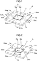
- FIG. 1 is a perspective view illustrating a wiring board A according to the present disclosure viewed from a side of one of its principal surfaces.
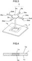
- FIG. 2 is a perspective view illustrating the wiring board A illustrated in FIG. 1 viewed from a side of the other of the principal surfaces, which is opposite to the one principal surface illustrated in FIG. 1 .
- FIG. 3 is an exploded perspective view illustrating the wiring board A illustrated in FIG. 2 .
- FIG. 4 is a cross-sectional view taken along a line iv-iv illustrated in FIG. 1 .
- FIG. 5 is a cross-sectional view taken along a line v-v illustrated in FIG. 1 .
- dashed lines in a part corresponding to a metal member 3 are illustrated for convenience of explanation in order to clarify that the metal member 3 is constituted of a stage part 3a and bridge parts 3b.
- the wiring board A includes a frame base material 1 and the metal member 3.
- the frame base material 1 constituting the wiring board A may be referred to as the first frame base material 1.
- the first frame base material 1 is formed in plate-shaped.
- the first frame base material 1 includes a through hole 1b in its central region 1a (see dashed line).
- the central region 1a is a region surrounding an intersection point of two diagonal lines C1L and C2L in a case where the first frame base material 1 is formed in rectangular-shaped as illustrated in FIGS. 1 and 2 .
- An area of the central region 1a has an arbitrary size because it depends on a size of an electric element to be mounted; however, roughly speaking, may be 0.1 to 0.3 when an area of a right face 1e to be mentioned later of the first frame base material 1 is one.
- the metal member 3 includes the stage part 3a and the bridge parts 3b.
- widths of the bridge parts 3b are equal to a width of the stage part 3a, or widths of the bridge parts 3b are narrower than a width of the stage part 3a.
- widths of the bridge parts 3b are equal to a width of the stage part 3a, a portion outer than the through hole 1b is the bridge parts 3b.
- the stage part 3a and the bridge parts 3b are preferably integrated with each other. In a case of the wiring board A illustrated in FIGS. 1 and 2 , the metal member 3 is in a state where the stage part 3a and the bridge parts 3b are exposed to a side of one (in FIG.
- the bridge parts 3b extend in a plurality of directions from the stage part 3a. In the wiring board A according to the present embodiment, the bridge parts 3b extend respective four directions from the stage part 3a. Thus, the first frame base material 1 is divided into four regions by the bridge parts 3b.
- FIGS. 1 and 2 an area of the stage part 3a is illustrated to be smaller than an opened area of the through hole 1b.
- a stage part 1a may be covered with a portion of the frame base material 1. Sizes of the stage part 3a and the through hole 1b are changed in FIGS. 1 and 2 for convenience of explanation so that they are able to be distinguished from each other.
- the stage part 3a may be preferably arranged such that at least a portion thereof is exposed from the through hole 1b.
- an area of a principal surface of the stage part 3a may preferably have a size corresponding to an area of the through hole 1b that is provided in the first frame base material 1.
- a size of an area of a principal surface of the stage part 3a, which corresponds to an area of the through hole 1b that is provided in the first frame base material 1, means that an area of the stage part 3a may be equal to an area of the through hole 1b provided in the first frame base material 1, or an area of the stage part 3a may be within a range of equal to or more than 0.90 and equal to or less than 1.1 in a case where an area of the through hole 1b is one. In this case, it is preferable that a shape of the stage part 3a and a shape of the through hole 1b may be nearly similar to each other.
- the stage part 3a may be arranged to be fitted to the through hole 1b.
- a width of the bridge parts 3b is narrower than a width of the stage part 3a, in other words, when a width of the stage part 3a is defined as w1 and a width of the bridge parts 3b is defined as w2, w1 and w2 are in a relation of w1 > w2.
- a shape of the stage part 3a in a plan view may be preferably square; however, not limited thereto, may be rectangular-shaped with a plurality of corners as long as the shape corresponds to the through hole 1b provided in the first frame base material 1. In this case, corners of the stage part 3a in a plan view may be rounded.
- the bridge part 3b may be formed in rectangular-shaped. As illustrated in FIGS. 1 and 2 , the bridge parts 3b extend in outer directions from the stage part 3a. The bridge parts 3b are arranged to be flush with the reverse face 1c of the first frame base material 1. Moreover, an end part 3bt of the bridge part 3b, which is opposite to the stage part 3a, is exposed on a side surface 1d of the first frame base material 1.
- a principal surface of the first frame base material 1 which is opposite to the reverse face 1c may be defined as the right face 1e.
- the stage part 3a constituted of the metal member 3 is arranged in the through hole 1b of the first frame base material 1. Principal surfaces of the stage part 3a are exposed to both sides of the right face 1e and the reverse face 1c of the first frame base material 1. Therefore, heat of the stage part 3a is able to be emitted from both of the surfaces of the stage part 3a. Thus, it is possible to improve heat dissipation from the wiring board A.
- the bridge parts 3b that are integrated with the stage part 3a are provided to the wiring board A. Moreover, the bridge parts 3b are exposed on the reverse face 1c of the first frame base material 1. Thus, it is possible to additionally execute heat dissipation from the bridge parts 3b.
- a heat radiation member such as a heatsink may be arranged in contact with the exposed bridge part 3b. Thus, it is possible to further improve heat dissipation of the wiring board A.
- the first frame base material 1 has a structure to be segmented by the bridge parts 3b extending, from the stage part 3a, in respective directions that are perpendicular to each other.
- the first frame base material 1 has a structure to be held by the bridge parts 3b extending, from the stage part 3a, in respective four directions.
- a width w2 of the bridge part 3b is narrower than a width w1 of the stage part 3a.
- An elastic modulus of the wiring board A in the region that is not covered with the bridge parts 3b is lower than that of a region that is covered with the bridge parts 3b by an amount corresponding to the non-covering bridge parts 3b.
- an elastic modulus of the first frame base material 1 is able to be lower than that of the metal member 3, and thus the first frame base material 1 may be formed of a material whose main component is organic resin.
- the first frame base material 1 is formed of a material whose main component is organic resin, it is preferable that electric conductive paste containing organic resin is applied to via electric conductors 5 and wiring parts 13, which are to be mentioned later.
- a metal component contained in the electric conductive paste at least one noble-metal material that is selected from a group of gold, silver, palladium, and platinum is preferable because reduction thereof in the electric conductivity due to oxidation is small.
- each of the bridge parts 3b includes a first principal surface 3ba, which is in contact with the first frame base material 1, and a second principal surface 3bb that is opposite to the first principal surface 3ba.
- the second principal surface 3bb is a principal surface that is not in contact with the first frame base material 1.
- each of the bridge parts 3b includes a side surface 3bc that is connected with the first principal surface 3ba and the second principal surface 3bb.
- the side surface 3bc of the bridge part 3b is arranged in a lateral direction (width direction) of the bridge part 3b.
- each of the bridge parts 3b includes an edge surface 3bd at its edge on a side opposite to the stage part 3a.
- each of the bridge parts 3b includes, in addition to the second principal surface 3bb that is not in contact with the first frame base material 1, a surface that is not in contact with the first frame base material 1 on the edge surface 3bd that is an edge of the corresponding bridge part 3b in its longitudinal direction, so that it is possible to further improve heat dissipation of the bridge parts 3b.
- FIG. 6 is a perspective view illustrating another mode of the wiring board according to the present disclosure.
- a wiring board B illustrated in FIG. 6 is obtained by providing the via electric conductors 5 to the wiring board A illustrated in FIG. 1 .
- FIG. 7 is a cross-sectional view taken along a line vii-vii illustrated in FIG. 6 .
- FIG. 8 is an enlarged cross-sectional view illustrating a portion P1 illustrated in FIG. 7.
- FIG. 9 is a cross-sectional view taken along a line ix-ix illustrated in FIG. 6 .
- FIG. 10 is an exploded perspective view illustrating the wiring board illustrated in FIG. 6 .
- the frame base material 1 includes the via electric conductor 5 in at least one of regions divided by the bridge parts 3b.
- the first frame base material 1 includes the via electric conductors 5 in respective four regions segmented by the bridge parts 3b.
- the regions segmented by the bridge parts 3b are provided with a reference symbol of 1f, and are regions each of which is surrounded by long dashed dotted lines. Regions 1f segmented by the bridge parts 3b are regions in which the first frame base material 1 is not covered with the bridge parts 3b.
- the via electric conductors 5 are arranged in regions in which the first frame base material 1 is not overlapped with the bridge parts 3b. In this case, the via electric conductors 5 penetrates through the first frame base material 1 in a thickness direction thereof.
- each of the via electric conductors 5, which penetrates through the first frame base material 1 in a thickness direction thereof, is arranged in a position that is closer to the stage part 3a than the side surface 1d of the first frame base material 1 constituting the wiring board B.
- heat that is generated in a side of one of principal surfaces of the wiring board B is able to be transferred to an opposite side from the via electric conductor 5 arranged in a position close to the stage part 3a.
- the wiring board B heat that is generated in a side of one of principal surfaces of the wiring board B is able to be transferred to an opposite side via a shorter detour and not via the side surface 1d of the first frame base material 1 from a principal surface of the stage part 3a. Furthermore, it is possible to transmit, via a shorter route, an electric signal from a side of one of principal surfaces of the wiring board B to the other principal surface thereof on an opposite side. Thus, it is possible to obtain a wiring board having a low inductance.
- the bridge parts 3b may be embedded in the first frame base material 1.
- a center portion 3bca in a thickness direction thereof on the side surface 3bc may protrude in a width direction thereof from a corresponding position 3bcb on a surface of the metal member 3 and a corresponding position 3bcc on a reverse face of the position 3bcb.
- the bridge parts 3b may have a shape obtained by removing a corner portion 3bd between the first principal surface 3ba or the second principal surface 3bb opposite thereto and the side surface 3bc.
- the center portion 3bca in a thickness direction of the bridge parts 3b may be acute-shaped.
- a part in which the center portion 3bca in a thickness direction thereof protrudes in a width direction thereof from the position 3bcb on the first principal surface 3ba and the position 3bcc on the second principal surface 3bb that is a reverse face may be formed not only on one side of the side surface 3bc of the bridge part 3b, but also on the two side surfaces 3bc directing opposite sides.
- the width direction of the bridge part 3b indicates a direction connecting two side surfaces 3bca illustrated in FIG. 8 .
- the side surface 3bc of the bridge part 3b has a shape obtained by removing the corner portion 3bd between the side surface 3bc and at least one of the first principal surface 3ba and the second principal surface 3bb
- an acute part (reference symbol P2) of the bridge part 3b is in a state where it penetrates into the first frame base material 1.
- the bridge part 3b is hardly peeled from the first frame base material 1 even in a state where the bridge part 3b is embedded near a surface of the first frame base material 1.
- a side surface of the stage part 3a may have a shape protruding in its width direction similarly to the bridge part 3b.
- a center portion 3aca in a thickness direction of a side surface 3ac of the stage part 3a may have a shape protruding its width direction from a position 3acb on a first principal surface 3aa of the stage part 3a and a position 3acc on a second principal surface 3ab that is on a reverse-face side.
- an end part 3at of the stage part 3a may be covered with a part of the first frame base material 1.
- the whole portion around the stage part 3a in the end part 3at of the stage part 3a is covered with a part of the first frame base material 1.
- the stage part 3a arranged in the through hole 1b of the first frame base material 1 is fixed to the through hole 1b by the part of the first frame base material 1.
- the stage part 3a is further hardly separated from the through hole 1b.
- the end parts 3at of the stage part 3a may be covered with a part of the first frame base material 1 from both sides (1d, 1e) in the thickness direction.
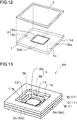
- FIG. 11 is a perspective view illustrating another mode of the wiring board according to the present disclosure.
- FIG. 12 is an exploded perspective view illustrating the wiring board illustrated in FIG. 11 .
- a wiring board C is able to be separated into the wiring board A and a metal frame member 7.
- the metal frame member 7 is bonded to at least the right face 1e of the frame base material 1 constituting the wiring board A.
- the right face 1e of the frame base material 1, which is bonded to the metal frame member 7, is a surface opposite to the reverse face 1c form which the bridge parts 3b are exposed.
- the metal frame member 7 may be bonded up to the side surface 1d of the frame base material 1. As illustrated in FIG.
- the metal frame member 7 in a case of a structure in which the metal frame member 7 is bonded to the wiring board A, it is possible to suppress a warp of the wiring board C.
- the bridge parts 3b are exposed from the reverse face 1c of the frame base material 1 as illustrated in the wiring board A, there presents a case where the reverse face 1c of the wiring board A is convexly deformed and further the right face 1e is concavely deformed.
- the wiring board C is capable of preventing such a warp to be generated in the wiring board A.
- FIG. 13 is a perspective view illustrating another mode of the wiring board according to the present disclosure.
- FIG. 14 is an exploded plan view illustrating layers of a wiring board AA illustrated in FIG. 13 .
- the wiring board AA illustrated in FIG. 13 has a structure in which a plate-shaped frame member 11 that includes a through hole 11b in its central region 11a is further laminated on the wiring board B.
- the above-mentioned wiring board B is a basic layer of the wiring board AA.
- the wiring board AA includes a wiring board D and a base-material layer E on or above the wiring board B.
- the wiring board D includes a frame base material 11 and the wiring parts 13.
- the frame base material 11 constituting the wiring board D may be referred to as the second frame base material 11.
- the base-material layer E is constituted of a frame base material 17.
- the frame base material 17 constituting the base-material layer E may be referred to as the third frame base material 17.
- the second frame base material 11 includes the through hole 11b in the central region 11a thereof.
- the third frame base material 17 also includes a through hole 17b in its central region 17a.
- areas of opening parts of the through hole 1b that is formed in the first frame base material 1 constituting the wiring board B, the through hole 11b that is formed in the second frame base material 11 constituting the wiring board D, and the through hole 17b that is formed in the third frame base material 17 constituting the base-material layer E increase step-by-step from a lower-layer side of the first frame base material 1 to an upper-layer side of the third frame base material 17.
- sizes of openings of the through holes 1b, 11b, and 17b increase step-by-step from a side of the stage part 3a to the upward side.
- a wiring board in which a light emitting element that diffuses light such as a Light Emitting Diode (LED), is mounted on the stage part 3a.
- a light emitting element that diffuses light such as a Light Emitting Diode (LED)
- the wiring parts 13 are arranged in a periphery of the through hole 11b.
- the wiring parts 13 may be arranged outer than respective sides of the through hole 11b.
- the wiring board D also includes via electric conductors 15 penetrating through the second frame base material 11 in its thickness direction.
- the via electric conductors 15 are arranged in the respective regions 1f that are segmented by the bridge parts 3b of the wiring board B. Moreover, the via electric conductors 15 is electrically connected to the wiring parts 13. Moreover, when the wiring board B and the wiring board D are laminated, the via electric conductors 5 of the wiring board B and the via electric conductors 15 of the wiring board D are electrically connected in their lamination direction.
- the via electric conductors 5 and 15 are arranged in the respective regions 1f segmented by the bridge parts 3b, and even in a case of a structure in which the plurality wiring board B and the wiring board D is laminated on the wiring board A so as to increase its thickness, it is still possible to maintain a low rigidity.
- the wiring board AA In the wiring board AA, an upper part of the stage part 3a has a cavity structure. Thus, an electric element arranged in the stage part 3a hardly receives a mechanical damage. Moreover, the wiring board AA has a structure in which the wiring board D and the base-material layer E are laminated not on a side of the reverse face 1c from which the bridge parts 3b of the wiring board B is exposed, but on a side a reverse face 1e that is opposite to the reverse face 1c, and thus heat dissipation is easily executed from the bridge parts 3b along with the stage part 3a that is exposed in the through hole 1b. As a result, it is possible to maintain a higher heat dissipation compared with a wiring board having a structure in which the stage part 3a alone is exposed.
- a bonding material is provided to a periphery of the through hole 17b which is an upper surface of the base-material layer E if necessary.
- the bonding material is for bonding to a lid part and the like.
- the metal frame member 7 may be arranged on an upper surface of the base-material layer E.
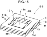
- FIG. 15 is a perspective view illustrating another mode of the wiring board according to the present disclosure.
- a different point between a wiring board BB illustrated in FIG. 15 and the wiring board AA illustrated in FIG. 13 is that an opening area of the through hole 11b that is formed in the second frame base material 11 constituting the wiring board D is approximately equal to an area of the stage part 3a in the wiring board B.
- the areas indicate an area of the stage part 3a in the wiring board B in a plan view of the wiring board BB and an area of the through hole 11b in the wiring board D in a plan view of the wiring board BB.
- an area of the through hole 11b in the wiring board D is set to approximately equal to an area of a stage part 3b in the wiring board B, and thus it is possible to obtain a structure in which the through hole 11b of the wiring board D more tightly surrounds the stage part 3a.
- the wiring board BB having such a structure is preferable for mounting thereon a light emitting element whose emitted light hardly diffuses in the stage part 3a and radiates in the vertical direction.
- a light emitting element a Laser Diode (LD), a Vertical Cavity Surface Emitting LASER (VICSEL), and the like are exemplified.
- FIG. 16 is a partially-exploded perspective view illustrating an electric device according to the present disclosure.
- An electric device AAA includes an electric element 25 on the stage part 3a provided at a center portion of the wiring board AA.
- the electric device AAA includes a lid part 27 on an upper surface of the base-material layer E in the wiring board AA.
- a basic layer of the electric device AAA illustrated in FIG. 16 is, i.e. the wiring board A in which the bridge parts 3b along with the stage part 3a are exposed from the reverse face 1c of the first frame base material 1.
- the wiring parts 13 arranged on a surface of the wiring board D is used for electrical connection to the electric element 25 on the stage part 3a of the wiring board D. In this case, wire bonding is commonly employed for electric connection (not illustrated) between the electric element 25 and the wiring parts 13.
- the electric element 25 is an integrated circuit such as an LSI, a substrate made of kovar or ceramic may be employed for the lid part 27.
- a transparent member such as a glass plate may be employed for the lid part 27 for transmitting therethrough light generated by the light emitting element.
- the light emitting element one selected from a group of a Light Emitting Diode (LED), a Laser Diode (LD), and a Vertical Cavity Surface Emitting LASER (VICSEL), and the like is preferable.
- the electric device AAA illustrated in FIG. 16 may be also provided with a heat radiation member such as a heatsink.
- a heat radiation member such as a heatsink.
- a manufacturing method of the wiring board B as one example will be explained.
- a base material to be the first frame base material 1 is prepared.
- metallic foil to be the metal member 3 is prepared.
- the first frame base material 1 is obtained by forming holes for the through hole 1b and the via electric conductors 5 in the base material by punching of a die, for example.
- the through hole 1b is formed in the central region 1a of the first frame base material 1. Holes are formed in a periphery of the through hole 1b in the first frame base material 1. The holes are formed by punching of a die or a LASER process.
- the base material is sheet-shaped and contains organic resin, and preferably is in semi-cured state.
- the organic resin preferably contains, as a main component, one selected from a group of epoxy resin, poly phenylene ether resin, olefin resin, and the like.
- the main component indicates a component whose content ratio is the highest of components contained in the base material.
- the first frame base material 1 obtained from a base material is in a state where the plurality of first frame base materials 1 is connected with each other.
- the metal member 3 obtained from metallic foil is in a state where the plurality of metal members 3 is connected with each other.
- the plurality of first frame base materials 1 that is connected with each other is defined as a mother base material.
- the plurality of the metal members 3 that is connected with each other is defined as a mother metal member.
- the metal members 3 (or mother metal member) is obtained by performing pattern processing on metallic foil with a method such as etching.
- metallic foil may be preferably employed because copper foil has a high electric conductivity and pattern processing is able to be performed on copper foil with a high size accuracy.
- Metal paste may be preferably employed for the via electric conductors 5.
- the mother base material and the mother metal member are laminated, and the first frame base material 1 and the metal member 3 are overlapped with each other so as to form a temporary laminated body.
- the metal member 3 is arranged such that the stage part 3a is arranged on the through hole 1b formed in the first frame base material 1, and the bridge parts 3b are regions that do not cover the via electric conductors 5 formed in the first frame base material 1.
- a pressure heat treatment is executed on the temporary laminated body under a predetermined condition so as to fabricate a laminated body to be a mother wiring board.
- the laminated body is cut into a piece having a predetermined size so as to obtain the wiring board B.
- the metal member 3 is prepared along with base materials to be the wiring board B, the wiring board D, and the base-material layer E.
- the via electric conductors 5 and 15 and the wiring parts 13 are preliminarily formed in base materials to be the wiring board B and the wiring board D.
- electric conductive paste may be employed for formation of the via electric conductors 5 and 15 and the wiring parts 13.
- the via electric conductors 5 and 15 and the wiring parts 13 are formed by printing electric conductive paste on a mother base material.
- the wiring board D is obtained by forming the through hole 11b and the via electric conductors 15 in the second frame base material 11 obtained by processing a base material, and then forming the wiring parts 13 on one of its principal surfaces.
- the third frame base material 17, which is obtained by forming the through hole 17b in a base material, is used for the base-material layer E.
- a mother base material in which the plurality of first frame base materials 1 is connected may be used instead of the first frame base material 1.
- mother base materials may be respectively used for the second frame base material 11 and the third frame base material 17.
- the electric device AAA When fabricating the electric device AAA, first, the above-mentioned wiring board AA is prepared, and then the electric element 25 is mounted on the stage part 3a of the wiring board AA. Next, with the use of bonding material, the lid part 27 is bonded to an upper surface of the base-material layer E that is an uppermost layer of the wiring board AA. It is preferable that the electric element 25 may be mounted on the stage part 3a or the lid part 27 may be bonded to an upper surface of the base-material layer E, with the use of a bonding material such as an organic resin represent by an epoxy resin, etc. or a low melting-point metal material represent by a solder or a gold-tin.
- a bonding material such as an organic resin represent by an epoxy resin, etc. or a low melting-point metal material represent by a solder or a gold-tin.
- the wiring board B, the wiring board AA, and the electric device AAA having a high heat dissipation and a small residual stress.
- a base material was prepared whose main component was epoxy resin. Slurry was molded by the doctor blade method so as to fabricate a plate-shaped base material. Next, holes for through holes and via electric conductors were formed in the base material so as to fabricate a mother base material in which a plurality of frame base materials was formed. Holes for the via electric conductors, which were formed in the frame base material, were filled with an electric conductive paste whose main component was silver so as to form the via electric conductors.
- An etching treatment was performed on a copper foil whose thickness was 200 ⁇ m so as to fabricate a metal member. Center portions in thickness directions of side surfaces of a stage part and bridge parts, which constituted the obtained metal member, had protruding shapes. A process was performed on the copper foil so as to obtain a shape of a mother metal member in which a plurality of metal members was connected.
- the fabricated mother base material and the fabricated mother metal member were laminated and pressurized heating was performed thereon so as to fabricate a mother wiring board that includes hundred wiring boards.
- a condition of the pressurized heating was that the maximum temperature was 200°C, pressure was 0.1 MPa, and a heating time interval was 5 hours.
- the mother wiring board was cut into pieces each having the following size so as to fabricate the wiring board illustrated in FIGS. 1 and 2 .
- a depth was 10 mm
- a width was 10 mm
- a thickness was 0.3 mm.
- An area of a stage part in the metal member had a depth of 5 mm and a width of 5 mm.
- the bridge parts had a width of 1 mm.
- the bridge parts extended in four directions from a stage part to be exposed from opposing side surfaces of the frame base material. A periphery portion of the stage part and the bridge parts were in a state where they were covered with a part of the frame base material.
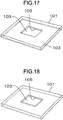
- FIG. 17 As illustrated in FIG. 17 , as a sample to be a comparison example, a sample obtained by sticking copper foil on the whole of a principal surface of the frame base material was fabricated. As illustrated in FIG. 18 , as another sample to be a comparison example, a wiring board including a metal member having a shape without bridge parts was fabricated. Reference symbols illustrated in FIGS. 17 and 18 indicate the following members. 101: Frame member, 103: Copper foil, 105: Through hole.
- the metal member without bridge parts was fabricated by the following process. First, a metal member having bridge parts was stuck on an organic film. Next, a stage part was coated with a resist film made of an epoxy resin. Next, an etching treatment was performed on a part of the bridge parts in the metal member, which was not covered with the resist film, so as to fabricate the metal member.
- FIG. 19 A method for evaluating heat dissipation is illustrated in FIG. 19 .
- Reference symbols illustrated in FIG. 19 indicate the following members.
- a sample for measuring heat dissipation was fabricated.
- An alumina substrate whose thickness was 0.2 mm was placed on a surface of a semiconductor element for test, a thermocouple was arranged on its upper surface and further was fixed by using potting resin so as to fabricate the sample for measuring heat dissipation.
- Heat dissipation was evaluated by the following method. First, electric current of 10 W was caused to flow into a semiconductor element (4 mm ⁇ 4 mm ⁇ 0.5 mm) for test in the atmosphere of 25°C for one minute. Next, the electric conduction was stopped, and after 10 seconds, a temperature (°C) of the surface of the semiconductor element was measured by using a thermocouple. Table 1 indicates a relative ratio when a temperature difference between a temperature (maximum temperature) of Sample No.3 and 25°C is one.
- FIG. 20 illustrates a method for indicating rigidity of a wiring board.
- Reference symbols illustrated in FIG. 20 indicate the following members.
- a pressure jig was attached to an autogragh machine and the center portion of a wiring board was pressured so as to evaluate rigidity of the wiring board.
- the maximum stress was obtained from stress-strain characteristics.
- a frame body whose size of an outer frame was 10 mm ⁇ 10 mm and width and thickness were 1 mm was arranged, as a spacer 127, under a wiring board of a sample.
- Table 1 a relative ratio is indicated when the maximum stress of Sample 3 is one.
- Sample No.1 As obvious from Table 1, compared with Sample No.3 fabricated by sticking copper foil on the approximately whole of one of principal surfaces of a first frame base material, heat dissipation of Sample No.1, which was fabricated by using a metal member including a stage part and bridge parts, reduced by 10%; however, compared with Sample No.2 that is fabricated by using a metal member including a stage part alone and without bridge parts, heat dissipation of Sample No.1 was high. Sample No.1 includes a region that was not covered with the bridge part so as to have a structure in which via electric conductors were able to be arranged near the semiconductor element. Thus, it contributed to reduction in the inductance.
- Sample No.3 had a structure in which copper foil was stuck on the approximately whole of one of principal surfaces of the first frame base material, and thus wiring from a semiconductor element to a reverse face of the wiring board was to go through a side-surface wire formed in a periphery of the wiring board by using a bonding wire, thereby leading to increase in the inductance.
- rigidity of a wiring board of Sample No.1 is low, and thus thermal stress in the wiring board was inclined to be eased.
- connection reliability of Sample No.1 when a wiring board was mounted on a mother board was high.
Landscapes
- Engineering & Computer Science (AREA)
- Microelectronics & Electronic Packaging (AREA)
- Manufacturing & Machinery (AREA)
- Structure Of Printed Boards (AREA)
- Cooling Or The Like Of Semiconductors Or Solid State Devices (AREA)
Abstract
Description
- The present disclosure relates to a wiring board and an electric device.
- Conventionally, as a wiring board for mounting thereon electric elements such as a semiconductor element and a light emitting element, there has been proposed a structure having a metal heat radiation member arranged in a region in which electric elements are provided, so as to diffuse heat generated by these electric elements (see
Patent Literature 1, for example). - Patent Literature 1: Japanese Patent Application Laid-open No.
H04-125953 - A wiring board according to the present disclosure includes: a frame base material; and a metal member, wherein the frame base material is formed in plate-shaped, and includes a through hole in a central region of the frame base material, the metal member includes a stage part and at least one bridge part, a width of the bridge part is equal to or narrower than a width of the stage part, the bridge part extending toward an outer side from the stage part, at least a part of the stage part is arranged to be exposed from the through hole, and the bridge part is arranged to be disposed facing the frame base material.
- In an electric device according to the present disclosure, an electric element is mounted on a wiring board.
-
-
FIG. 1 is a perspective view illustrating a wiring board according to the present disclosure viewed from a side of one of its principal surfaces. -
FIG. 2 is a perspective view illustrating the wiring board illustrated inFIG. 1 viewed from a side of the other of the principal surfaces, which is opposite to the one principal surface illustrated inFIG. 1 . -
FIG. 3 is an exploded perspective view illustrating the wiring board illustrated inFIG. 2 . -
FIG. 4 is a cross-sectional view taken along a line iv-iv illustrated inFIG. 1 . -
FIG. 5 is a cross-sectional view taken along a line v-v illustrated inFIG. 1 . -
FIG. 6 is a perspective view illustrating another mode of the wiring board according to the present disclosure. -
FIG. 7 is a cross-sectional view taken along a line vii-vii illustrated inFIG. 6 . -
FIG. 8 is an enlarged cross-sectional view illustrating a portion P1 illustrated inFIG. 7 . -
FIG. 9 is a cross-sectional view taken along a line ix-ix illustrated inFIG. 6 . -
FIG. 10 is an exploded perspective view illustrating the wiring board illustrated inFIG. 6 . -
FIG. 11 is a perspective view illustrating another mode of the wiring board according to the present disclosure. -
FIG. 12 is a partially-exploded perspective view illustrating the wiring board illustrated inFIG. 10 . -
FIG. 13 is a perspective view illustrating another mode of the wiring board according to the present disclosure. -
FIG. 14 is an exploded plan view illustrating layers of the wiring board illustrated inFIG. 13 . -
FIG. 15 is a perspective view illustrating another mode of the wiring board according to the present disclosure. -
FIG. 16 is a partially-exploded perspective view illustrating an electric device according to the present disclosure. -
FIG. 17 is a perspective view illustrating a sample of another wiring board. -
FIG. 18 is a perspective view illustrating a sample of another wiring board. -
FIG. 19 is a perspective view schematically illustrating a method for evaluating heat dissipation of the sample. -
FIG. 20 is a cross-sectional view schematically illustrating a method for evaluating rigidity of the sample. Description of Embodiments -
FIG. 1 is a perspective view illustrating a wiring board A according to the present disclosure viewed from a side of one of its principal surfaces.FIG. 2 is a perspective view illustrating the wiring board A illustrated inFIG. 1 viewed from a side of the other of the principal surfaces, which is opposite to the one principal surface illustrated inFIG. 1 .FIG. 3 is an exploded perspective view illustrating the wiring board A illustrated inFIG. 2 .FIG. 4 is a cross-sectional view taken along a line iv-iv illustrated inFIG. 1 .FIG. 5 is a cross-sectional view taken along a line v-v illustrated inFIG. 1 . InFIG. 5 , dashed lines in a part corresponding to ametal member 3 are illustrated for convenience of explanation in order to clarify that themetal member 3 is constituted of astage part 3a andbridge parts 3b. - The wiring board A according to embodiments includes a
frame base material 1 and themetal member 3. Hereinafter, theframe base material 1 constituting the wiring board A may be referred to as the firstframe base material 1. The firstframe base material 1 is formed in plate-shaped. In a plan view, the firstframe base material 1 includes a throughhole 1b in itscentral region 1a (see dashed line). Thecentral region 1a is a region surrounding an intersection point of two diagonal lines C1L and C2L in a case where the firstframe base material 1 is formed in rectangular-shaped as illustrated inFIGS. 1 and 2 . An area of thecentral region 1a has an arbitrary size because it depends on a size of an electric element to be mounted; however, roughly speaking, may be 0.1 to 0.3 when an area of aright face 1e to be mentioned later of the firstframe base material 1 is one. - The
metal member 3 includes thestage part 3a and thebridge parts 3b. In this case, widths of thebridge parts 3b are equal to a width of thestage part 3a, or widths of thebridge parts 3b are narrower than a width of thestage part 3a. When widths of thebridge parts 3b are equal to a width of thestage part 3a, a portion outer than thethrough hole 1b is thebridge parts 3b. Thestage part 3a and thebridge parts 3b are preferably integrated with each other. In a case of the wiring board A illustrated inFIGS. 1 and 2 , themetal member 3 is in a state where thestage part 3a and thebridge parts 3b are exposed to a side of one (inFIG. 2 , surface on whichmetal member 3 is laminated; hereinafter, may be referred to asreverse face 1c) of principal surfaces of the firstframe base material 1. Thebridge parts 3b extend in a plurality of directions from thestage part 3a. In the wiring board A according to the present embodiment, thebridge parts 3b extend respective four directions from thestage part 3a. Thus, the firstframe base material 1 is divided into four regions by thebridge parts 3b. - Herein, sizes and shapes of the
stage part 3a and thebridge parts 3b will be explained. InFIGS. 1 and 2 , an area of thestage part 3a is illustrated to be smaller than an opened area of thethrough hole 1b. Note that as described below, astage part 1a may be covered with a portion of theframe base material 1. Sizes of thestage part 3a and the throughhole 1b are changed inFIGS. 1 and 2 for convenience of explanation so that they are able to be distinguished from each other. In this case, thestage part 3a may be preferably arranged such that at least a portion thereof is exposed from the throughhole 1b. In a plan view of the firstframe base material 1, an area of a principal surface of thestage part 3a may preferably have a size corresponding to an area of thethrough hole 1b that is provided in the firstframe base material 1. A size of an area of a principal surface of thestage part 3a, which corresponds to an area of thethrough hole 1b that is provided in the firstframe base material 1, means that an area of thestage part 3a may be equal to an area of thethrough hole 1b provided in the firstframe base material 1, or an area of thestage part 3a may be within a range of equal to or more than 0.90 and equal to or less than 1.1 in a case where an area of thethrough hole 1b is one. In this case, it is preferable that a shape of thestage part 3a and a shape of thethrough hole 1b may be nearly similar to each other. Thestage part 3a may be arranged to be fitted to the throughhole 1b. - Next, as illustrated in
FIG. 2 , it is preferable that a width of thebridge parts 3b is narrower than a width of thestage part 3a, in other words, when a width of thestage part 3a is defined as w1 and a width of thebridge parts 3b is defined as w2, w1 and w2 are in a relation of w1 > w2. In this case, a shape of thestage part 3a in a plan view may be preferably square; however, not limited thereto, may be rectangular-shaped with a plurality of corners as long as the shape corresponds to the throughhole 1b provided in the firstframe base material 1. In this case, corners of thestage part 3a in a plan view may be rounded. - The
bridge part 3b may be formed in rectangular-shaped. As illustrated inFIGS. 1 and 2 , thebridge parts 3b extend in outer directions from thestage part 3a. Thebridge parts 3b are arranged to be flush with thereverse face 1c of the firstframe base material 1. Moreover, an end part 3bt of thebridge part 3b, which is opposite to thestage part 3a, is exposed on aside surface 1d of the firstframe base material 1. Hereinafter, a principal surface of the firstframe base material 1 which is opposite to thereverse face 1c may be defined as theright face 1e. - In the wiring board A, the
stage part 3a constituted of themetal member 3 is arranged in the throughhole 1b of the firstframe base material 1. Principal surfaces of thestage part 3a are exposed to both sides of theright face 1e and thereverse face 1c of the firstframe base material 1. Therefore, heat of thestage part 3a is able to be emitted from both of the surfaces of thestage part 3a. Thus, it is possible to improve heat dissipation from the wiring board A. - As described above, the
bridge parts 3b that are integrated with thestage part 3a are provided to the wiring board A. Moreover, thebridge parts 3b are exposed on thereverse face 1c of the firstframe base material 1. Thus, it is possible to additionally execute heat dissipation from thebridge parts 3b. - A heat radiation member such as a heatsink may be arranged in contact with the exposed
bridge part 3b. Thus, it is possible to further improve heat dissipation of the wiring board A. - In a case of the wiring board A, the first
frame base material 1 has a structure to be segmented by thebridge parts 3b extending, from thestage part 3a, in respective directions that are perpendicular to each other. In other words, the firstframe base material 1 has a structure to be held by thebridge parts 3b extending, from thestage part 3a, in respective four directions. Thus, it is possible to improve flatness of the wiring board A. In this case, a width w2 of thebridge part 3b is narrower than a width w1 of thestage part 3a. Thus, on the firstframe base material 1, there presents a region in a periphery of thestage part 3a, which is not covered with thebridge parts 3b. An elastic modulus of the wiring board A in the region that is not covered with thebridge parts 3b is lower than that of a region that is covered with thebridge parts 3b by an amount corresponding to thenon-covering bridge parts 3b. As a result, even when a distortion occurs in the wiring board A, the firstframe base material 1 is easily deformed in the region where thebridge part 3b is not present. Thus, it is possible to reduce the stress that occurs in the wiring board A. As a result, in a case where the wiring board A has a structure to be mounted on a mother board or the like, high connection reliability is able to be obtained. In this case, an elastic modulus of the firstframe base material 1 is able to be lower than that of themetal member 3, and thus the firstframe base material 1 may be formed of a material whose main component is organic resin. When the firstframe base material 1 is formed of a material whose main component is organic resin, it is preferable that electric conductive paste containing organic resin is applied to viaelectric conductors 5 andwiring parts 13, which are to be mentioned later. In this case, as a metal component contained in the electric conductive paste, at least one noble-metal material that is selected from a group of gold, silver, palladium, and platinum is preferable because reduction thereof in the electric conductivity due to oxidation is small. - Next, shapes of the
bridge parts 3b constituting themetal member 3 will be more specifically explained. As illustrated inFIGS. 1 to 5 , each of thebridge parts 3b includes a first principal surface 3ba, which is in contact with the firstframe base material 1, and a second principal surface 3bb that is opposite to the first principal surface 3ba. In this case, the second principal surface 3bb is a principal surface that is not in contact with the firstframe base material 1. As illustrated inFIG. 3 , each of thebridge parts 3b includes a side surface 3bc that is connected with the first principal surface 3ba and the second principal surface 3bb. The side surface 3bc of thebridge part 3b is arranged in a lateral direction (width direction) of thebridge part 3b. Moreover, each of thebridge parts 3b includes an edge surface 3bd at its edge on a side opposite to thestage part 3a. - According to the wiring board A, each of the
bridge parts 3b includes, in addition to the second principal surface 3bb that is not in contact with the firstframe base material 1, a surface that is not in contact with the firstframe base material 1 on the edge surface 3bd that is an edge of the correspondingbridge part 3b in its longitudinal direction, so that it is possible to further improve heat dissipation of thebridge parts 3b. -
FIG. 6 is a perspective view illustrating another mode of the wiring board according to the present disclosure. A wiring board B illustrated inFIG. 6 is obtained by providing the viaelectric conductors 5 to the wiring board A illustrated inFIG. 1 .FIG. 7 is a cross-sectional view taken along a line vii-vii illustrated inFIG. 6 .FIG. 8 is an enlarged cross-sectional view illustrating a portion P1 illustrated inFIG. 7. FIG. 9 is a cross-sectional view taken along a line ix-ix illustrated inFIG. 6 .FIG. 10 is an exploded perspective view illustrating the wiring board illustrated inFIG. 6 . In a wiring board according to the embodiments, it is preferable that theframe base material 1 includes the viaelectric conductor 5 in at least one of regions divided by thebridge parts 3b. In the wiring board B, the firstframe base material 1 includes the viaelectric conductors 5 in respective four regions segmented by thebridge parts 3b. InFIG. 6 , the regions segmented by thebridge parts 3b are provided with a reference symbol of 1f, and are regions each of which is surrounded by long dashed dotted lines.Regions 1f segmented by thebridge parts 3b are regions in which the firstframe base material 1 is not covered with thebridge parts 3b. - In other words, in the wiring board B, the via
electric conductors 5 are arranged in regions in which the firstframe base material 1 is not overlapped with thebridge parts 3b. In this case, the viaelectric conductors 5 penetrates through the firstframe base material 1 in a thickness direction thereof. - As illustrated in
FIG. 6 , each of the viaelectric conductors 5, which penetrates through the firstframe base material 1 in a thickness direction thereof, is arranged in a position that is closer to thestage part 3a than theside surface 1d of the firstframe base material 1 constituting the wiring board B. Thus, heat that is generated in a side of one of principal surfaces of the wiring board B is able to be transferred to an opposite side from the viaelectric conductor 5 arranged in a position close to thestage part 3a. In other words, in the wiring board B, heat that is generated in a side of one of principal surfaces of the wiring board B is able to be transferred to an opposite side via a shorter detour and not via theside surface 1d of the firstframe base material 1 from a principal surface of thestage part 3a. Furthermore, it is possible to transmit, via a shorter route, an electric signal from a side of one of principal surfaces of the wiring board B to the other principal surface thereof on an opposite side. Thus, it is possible to obtain a wiring board having a low inductance. - In the above-mentioned wiring boards A and B, the
bridge parts 3b may be embedded in the firstframe base material 1. In this case, in thebridge part 3b, a center portion 3bca in a thickness direction thereof on the side surface 3bc may protrude in a width direction thereof from a corresponding position 3bcb on a surface of themetal member 3 and a corresponding position 3bcc on a reverse face of the position 3bcb. - In other words, in a cross-sectional view, the
bridge parts 3b may have a shape obtained by removing a corner portion 3bd between the first principal surface 3ba or the second principal surface 3bb opposite thereto and the side surface 3bc. Particularly, the center portion 3bca in a thickness direction of thebridge parts 3b may be acute-shaped. In this case, in thebridge part 3b, a part in which the center portion 3bca in a thickness direction thereof protrudes in a width direction thereof from the position 3bcb on the first principal surface 3ba and the position 3bcc on the second principal surface 3bb that is a reverse face may be formed not only on one side of the side surface 3bc of thebridge part 3b, but also on the two side surfaces 3bc directing opposite sides. Note that the width direction of thebridge part 3b indicates a direction connecting two side surfaces 3bca illustrated inFIG. 8 . - In a case where the side surface 3bc of the
bridge part 3b has a shape obtained by removing the corner portion 3bd between the side surface 3bc and at least one of the first principal surface 3ba and the second principal surface 3bb, when thebridge part 3b is embedded in the firstframe base material 1, an acute part (reference symbol P2) of thebridge part 3b is in a state where it penetrates into the firstframe base material 1. Thus, thebridge part 3b is hardly peeled from the firstframe base material 1 even in a state where thebridge part 3b is embedded near a surface of the firstframe base material 1. - Moreover, as illustrated in
FIG. 9 , a side surface of thestage part 3a may have a shape protruding in its width direction similarly to thebridge part 3b. Specifically, a center portion 3aca in a thickness direction of a side surface 3ac of thestage part 3a may have a shape protruding its width direction from a position 3acb on a first principal surface 3aa of thestage part 3a and a position 3acc on a second principal surface 3ab that is on a reverse-face side. When thestage part 3a has such a shape illustrated inFIG. 9 , an end part 3at of thestage part 3a may be covered with a part of the firstframe base material 1. In this case, it is preferable that the whole portion around thestage part 3a in the end part 3at of thestage part 3a is covered with a part of the firstframe base material 1. When the end part 3at of thestage part 3a has a structure that is covered with a part of the firstframe base material 1, thestage part 3a arranged in the throughhole 1b of the firstframe base material 1 is fixed to the throughhole 1b by the part of the firstframe base material 1. Thus, thestage part 3a is further hardly separated from the throughhole 1b. In this case, the end parts 3at of thestage part 3a may be covered with a part of the firstframe base material 1 from both sides (1d, 1e) in the thickness direction. -
FIG. 11 is a perspective view illustrating another mode of the wiring board according to the present disclosure.FIG. 12 is an exploded perspective view illustrating the wiring board illustrated inFIG. 11 . As illustrated inFIG. 12 , a wiring board C is able to be separated into the wiring board A and ametal frame member 7. Themetal frame member 7 is bonded to at least theright face 1e of theframe base material 1 constituting the wiring board A. Theright face 1e of theframe base material 1, which is bonded to themetal frame member 7, is a surface opposite to thereverse face 1c form which thebridge parts 3b are exposed. In this case, themetal frame member 7 may be bonded up to theside surface 1d of theframe base material 1. As illustrated inFIG. 11 , in a case of a structure in which themetal frame member 7 is bonded to the wiring board A, it is possible to suppress a warp of the wiring board C. In a case of a structure in which thebridge parts 3b are exposed from thereverse face 1c of theframe base material 1 as illustrated in the wiring board A, there presents a case where thereverse face 1c of the wiring board A is convexly deformed and further theright face 1e is concavely deformed. The wiring board C is capable of preventing such a warp to be generated in the wiring board A. -
FIG. 13 is a perspective view illustrating another mode of the wiring board according to the present disclosure.FIG. 14 is an exploded plan view illustrating layers of a wiring board AA illustrated inFIG. 13 . The wiring board AA illustrated inFIG. 13 has a structure in which a plate-shapedframe member 11 that includes a throughhole 11b in its central region 11a is further laminated on the wiring board B. In this case, the above-mentioned wiring board B is a basic layer of the wiring board AA. The wiring board AA includes a wiring board D and a base-material layer E on or above the wiring board B. The wiring board D includes aframe base material 11 and thewiring parts 13. Theframe base material 11 constituting the wiring board D may be referred to as the secondframe base material 11. The base-material layer E is constituted of aframe base material 17. Hereinafter, theframe base material 17 constituting the base-material layer E may be referred to as the thirdframe base material 17. The secondframe base material 11 includes the throughhole 11b in the central region 11a thereof. The thirdframe base material 17 also includes a throughhole 17b in itscentral region 17a. - In a case of the wiring board AA, areas of opening parts of the through
hole 1b that is formed in the firstframe base material 1 constituting the wiring board B, the throughhole 11b that is formed in the secondframe base material 11 constituting the wiring board D, and the throughhole 17b that is formed in the thirdframe base material 17 constituting the base-material layer E increase step-by-step from a lower-layer side of the firstframe base material 1 to an upper-layer side of the thirdframe base material 17. In other words, sizes of openings of the throughholes stage part 3a to the upward side. Thus, it is preferable for a wiring board in which a light emitting element that diffuses light, such as a Light Emitting Diode (LED), is mounted on thestage part 3a. - In the wiring board AA, the
wiring parts 13 are arranged in a periphery of the throughhole 11b. In a case of the wiring board D illustrated inFIGS. 13 and14 , thewiring parts 13 may be arranged outer than respective sides of the throughhole 11b. - The wiring board D also includes via
electric conductors 15 penetrating through the secondframe base material 11 in its thickness direction. The viaelectric conductors 15 are arranged in therespective regions 1f that are segmented by thebridge parts 3b of the wiring board B. Moreover, the viaelectric conductors 15 is electrically connected to thewiring parts 13. Moreover, when the wiring board B and the wiring board D are laminated, the viaelectric conductors 5 of the wiring board B and the viaelectric conductors 15 of the wiring board D are electrically connected in their lamination direction. - In the wiring board AA, even in a case of a structure in which the above-mentioned wiring board AA includes the plurality of via
electric conductors electric conductors respective regions 1f segmented by thebridge parts 3b, and even in a case of a structure in which the plurality wiring board B and the wiring board D is laminated on the wiring board A so as to increase its thickness, it is still possible to maintain a low rigidity. - In the wiring board AA, an upper part of the
stage part 3a has a cavity structure. Thus, an electric element arranged in thestage part 3a hardly receives a mechanical damage. Moreover, the wiring board AA has a structure in which the wiring board D and the base-material layer E are laminated not on a side of thereverse face 1c from which thebridge parts 3b of the wiring board B is exposed, but on a side areverse face 1e that is opposite to thereverse face 1c, and thus heat dissipation is easily executed from thebridge parts 3b along with thestage part 3a that is exposed in the throughhole 1b. As a result, it is possible to maintain a higher heat dissipation compared with a wiring board having a structure in which thestage part 3a alone is exposed. - Although not illustrated in
FIGS. 13 and14 , a bonding material is provided to a periphery of the throughhole 17b which is an upper surface of the base-material layer E if necessary. The bonding material is for bonding to a lid part and the like. In this case, in the wiring board AA, themetal frame member 7 may be arranged on an upper surface of the base-material layer E. Thus, it is possible to reduce a warp similarly to the case of the wiring board A. -
FIG. 15 is a perspective view illustrating another mode of the wiring board according to the present disclosure. A different point between a wiring board BB illustrated inFIG. 15 and the wiring board AA illustrated inFIG. 13 is that an opening area of the throughhole 11b that is formed in the secondframe base material 11 constituting the wiring board D is approximately equal to an area of thestage part 3a in the wiring board B. Herein, the areas indicate an area of thestage part 3a in the wiring board B in a plan view of the wiring board BB and an area of the throughhole 11b in the wiring board D in a plan view of the wiring board BB. In the wiring board BB illustrated inFIG. 15 , an area of the throughhole 11b in the wiring board D is set to approximately equal to an area of astage part 3b in the wiring board B, and thus it is possible to obtain a structure in which the throughhole 11b of the wiring board D more tightly surrounds thestage part 3a. The wiring board BB having such a structure is preferable for mounting thereon a light emitting element whose emitted light hardly diffuses in thestage part 3a and radiates in the vertical direction. As such a light emitting element, a Laser Diode (LD), a Vertical Cavity Surface Emitting LASER (VICSEL), and the like are exemplified. -
FIG. 16 is a partially-exploded perspective view illustrating an electric device according to the present disclosure. An electric device AAA includes anelectric element 25 on thestage part 3a provided at a center portion of the wiring board AA. The electric device AAA includes alid part 27 on an upper surface of the base-material layer E in the wiring board AA. A basic layer of the electric device AAA illustrated inFIG. 16 is, i.e. the wiring board A in which thebridge parts 3b along with thestage part 3a are exposed from thereverse face 1c of the firstframe base material 1. In the wiring board AA constituting the electric device AAA, thewiring parts 13 arranged on a surface of the wiring board D is used for electrical connection to theelectric element 25 on thestage part 3a of the wiring board D. In this case, wire bonding is commonly employed for electric connection (not illustrated) between theelectric element 25 and thewiring parts 13. - When the
electric element 25 is an integrated circuit such as an LSI, a substrate made of kovar or ceramic may be employed for thelid part 27. When theelectric element 25 is a light emitting element, a transparent member such as a glass plate may be employed for thelid part 27 for transmitting therethrough light generated by the light emitting element. In this case, as the light emitting element, one selected from a group of a Light Emitting Diode (LED), a Laser Diode (LD), and a Vertical Cavity Surface Emitting LASER (VICSEL), and the like is preferable. - The electric device AAA illustrated in
FIG. 16 may be also provided with a heat radiation member such as a heatsink. Similarly to the case of the above-mentioned wiring board A, a side of thereverse face 1c of the firstframe base material 1, from which both of thestage part 3a and thebridge parts 3b are exposed, is preferable for a position in which a heat radiation member is arranged for the reason of improvement in thermal conductivity. - Next, with reference to
FIG. 10 , a manufacturing method of the wiring board B as one example will be explained. When fabricating the wiring board B, first, a base material to be the firstframe base material 1 is prepared. Additionally, metallic foil to be themetal member 3 is prepared. - The first
frame base material 1 is obtained by forming holes for the throughhole 1b and the viaelectric conductors 5 in the base material by punching of a die, for example. The throughhole 1b is formed in thecentral region 1a of the firstframe base material 1. Holes are formed in a periphery of the throughhole 1b in the firstframe base material 1. The holes are formed by punching of a die or a LASER process. - The base material is sheet-shaped and contains organic resin, and preferably is in semi-cured state. The organic resin preferably contains, as a main component, one selected from a group of epoxy resin, poly phenylene ether resin, olefin resin, and the like. Herein, the main component indicates a component whose content ratio is the highest of components contained in the base material.
- Commonly, the first
frame base material 1 obtained from a base material is in a state where the plurality of firstframe base materials 1 is connected with each other. Furthermore, themetal member 3 obtained from metallic foil is in a state where the plurality ofmetal members 3 is connected with each other. The plurality of firstframe base materials 1 that is connected with each other is defined as a mother base material. The plurality of themetal members 3 that is connected with each other is defined as a mother metal member. - The metal members 3 (or mother metal member) is obtained by performing pattern processing on metallic foil with a method such as etching. For the metallic foil, copper foil may be preferably employed because copper foil has a high electric conductivity and pattern processing is able to be performed on copper foil with a high size accuracy. Metal paste may be preferably employed for the via
electric conductors 5. - Next, the mother base material and the mother metal member are laminated, and the first
frame base material 1 and themetal member 3 are overlapped with each other so as to form a temporary laminated body. In this case, themetal member 3 is arranged such that thestage part 3a is arranged on the throughhole 1b formed in the firstframe base material 1, and thebridge parts 3b are regions that do not cover the viaelectric conductors 5 formed in the firstframe base material 1. Next, a pressure heat treatment is executed on the temporary laminated body under a predetermined condition so as to fabricate a laminated body to be a mother wiring board. Finally, the laminated body is cut into a piece having a predetermined size so as to obtain the wiring board B. - Next, a manufacturing method of the wiring board AA as an example will be explained with reference to
FIG. 14 . When fabricating the wiring board AA, first, themetal member 3 is prepared along with base materials to be the wiring board B, the wiring board D, and the base-material layer E. In this case, it is preferable that the viaelectric conductors wiring parts 13 are preliminarily formed in base materials to be the wiring board B and the wiring board D. For example, electric conductive paste may be employed for formation of the viaelectric conductors wiring parts 13. The viaelectric conductors wiring parts 13 are formed by printing electric conductive paste on a mother base material. - Specifically, the wiring board D is obtained by forming the through
hole 11b and the viaelectric conductors 15 in the secondframe base material 11 obtained by processing a base material, and then forming thewiring parts 13 on one of its principal surfaces. The thirdframe base material 17, which is obtained by forming the throughhole 17b in a base material, is used for the base-material layer E. In this case, for example, a mother base material in which the plurality of firstframe base materials 1 is connected may be used instead of the firstframe base material 1. Similarly, mother base materials may be respectively used for the secondframe base material 11 and the thirdframe base material 17. - Next, base materials to be the wiring board B, the wiring board D, and the base-material layer E are aligned, along with the through
holes electric conductors - When fabricating the electric device AAA, first, the above-mentioned wiring board AA is prepared, and then the
electric element 25 is mounted on thestage part 3a of the wiring board AA. Next, with the use of bonding material, thelid part 27 is bonded to an upper surface of the base-material layer E that is an uppermost layer of the wiring board AA. It is preferable that theelectric element 25 may be mounted on thestage part 3a or thelid part 27 may be bonded to an upper surface of the base-material layer E, with the use of a bonding material such as an organic resin represent by an epoxy resin, etc. or a low melting-point metal material represent by a solder or a gold-tin. - According to the above-mentioned manufacturing method, it is possible to obtain the wiring board B, the wiring board AA, and the electric device AAA having a high heat dissipation and a small residual stress.
- First, a base material was prepared whose main component was epoxy resin. Slurry was molded by the doctor blade method so as to fabricate a plate-shaped base material. Next, holes for through holes and via electric conductors were formed in the base material so as to fabricate a mother base material in which a plurality of frame base materials was formed. Holes for the via electric conductors, which were formed in the frame base material, were filled with an electric conductive paste whose main component was silver so as to form the via electric conductors.
- An etching treatment was performed on a copper foil whose thickness was 200 µm so as to fabricate a metal member. Center portions in thickness directions of side surfaces of a stage part and bridge parts, which constituted the obtained metal member, had protruding shapes. A process was performed on the copper foil so as to obtain a shape of a mother metal member in which a plurality of metal members was connected.
- Next, the fabricated mother base material and the fabricated mother metal member were laminated and pressurized heating was performed thereon so as to fabricate a mother wiring board that includes hundred wiring boards. A condition of the pressurized heating was that the maximum temperature was 200°C, pressure was 0.1 MPa, and a heating time interval was 5 hours. Next, the mother wiring board was cut into pieces each having the following size so as to fabricate the wiring board illustrated in
FIGS. 1 and 2 . - Regarding a size of the frame base material, a depth was 10 mm, a width was 10 mm, and a thickness was 0.3 mm. An area of a stage part in the metal member had a depth of 5 mm and a width of 5 mm. The bridge parts had a width of 1 mm. The bridge parts extended in four directions from a stage part to be exposed from opposing side surfaces of the frame base material. A periphery portion of the stage part and the bridge parts were in a state where they were covered with a part of the frame base material.
- As illustrated in
FIG. 17 , as a sample to be a comparison example, a sample obtained by sticking copper foil on the whole of a principal surface of the frame base material was fabricated. As illustrated inFIG. 18 , as another sample to be a comparison example, a wiring board including a metal member having a shape without bridge parts was fabricated. Reference symbols illustrated inFIGS. 17 and 18 indicate the following members. 101: Frame member, 103: Copper foil, 105: Through hole. - The metal member without bridge parts was fabricated by the following process. First, a metal member having bridge parts was stuck on an organic film. Next, a stage part was coated with a resist film made of an epoxy resin. Next, an etching treatment was performed on a part of the bridge parts in the metal member, which was not covered with the resist film, so as to fabricate the metal member.
- A method for evaluating heat dissipation is illustrated in
FIG. 19 . Reference symbols illustrated inFIG. 19 indicate the following members. 111: Wiring board, 113: Semiconductor element, 115: Alumina substrate, 117: Thermocouple. Next, a sample for measuring heat dissipation was fabricated. An alumina substrate whose thickness was 0.2 mm was placed on a surface of a semiconductor element for test, a thermocouple was arranged on its upper surface and further was fixed by using potting resin so as to fabricate the sample for measuring heat dissipation. - Heat dissipation was evaluated by the following method. First, electric current of 10 W was caused to flow into a semiconductor element (4 mm × 4 mm × 0.5 mm) for test in the atmosphere of 25°C for one minute. Next, the electric conduction was stopped, and after 10 seconds, a temperature (°C) of the surface of the semiconductor element was measured by using a thermocouple. Table 1 indicates a relative ratio when a temperature difference between a temperature (maximum temperature) of Sample No.3 and 25°C is one.
-
FIG. 20 illustrates a method for indicating rigidity of a wiring board. Reference symbols illustrated inFIG. 20 indicate the following members. 120: Wiring board, 121: Frame base material, 123: Metal member, 125: Pressure jig, 127: Spacer. A pressure jig was attached to an autogragh machine and the center portion of a wiring board was pressured so as to evaluate rigidity of the wiring board. In this case, the maximum stress was obtained from stress-strain characteristics. In this case, a frame body whose size of an outer frame was 10 mm × 10 mm and width and thickness were 1 mm was arranged, as aspacer 127, under a wiring board of a sample. In Table 1, a relative ratio is indicated when the maximum stress ofSample 3 is one. Heat dissipation and rigidity indicated in Table 1 were calculated from an average value of values obtained by measuring 10 pieces for each of the samples.Table 1 Sample No. Structure of Wiring Board Heat Dissipation Rigidity Relative Ratio of Temperature Relative Ratio of Maximum Stress 1 FIG. 1 (FIG. 2 )0.9 0.6 2 FIG. 18 0.4 0.2 3 FIG. 17 1 1 - As obvious from Table 1, compared with Sample No.3 fabricated by sticking copper foil on the approximately whole of one of principal surfaces of a first frame base material, heat dissipation of Sample No.1, which was fabricated by using a metal member including a stage part and bridge parts, reduced by 10%; however, compared with Sample No.2 that is fabricated by using a metal member including a stage part alone and without bridge parts, heat dissipation of Sample No.1 was high. Sample No.1 includes a region that was not covered with the bridge part so as to have a structure in which via electric conductors were able to be arranged near the semiconductor element. Thus, it contributed to reduction in the inductance. In this point, Sample No.3 had a structure in which copper foil was stuck on the approximately whole of one of principal surfaces of the first frame base material, and thus wiring from a semiconductor element to a reverse face of the wiring board was to go through a side-surface wire formed in a periphery of the wiring board by using a bonding wire, thereby leading to increase in the inductance. Compared with Sample No.3, rigidity of a wiring board of Sample No.1 is low, and thus thermal stress in the wiring board was inclined to be eased. Compared with Sample No.3, connection reliability of Sample No.1 when a wiring board was mounted on a mother board was high.
-
- A, B, C, D, AA, BB
- Wiring board
- AAA
- Electric device
- E
- Base-material layer
- 1
- Frame base material (First frame base material)
- 1a,
- 11a, 17a Central region
- 1b,
- 11b, 17b Through hole
- 1c
- Reverse face
- 1d
- Side surface
- 1e
- Right face
- 1f
- Region segmented by bridge parts
- 3
- Metal member
- 3a
- Stage part
- 3at
- End part of stage part
- 3b
- Bridge part
- 3ba
- First principal surface
- 3bb
- Second principal surface
- 3bc
- Side surface
- 3bd
- Corner portion
- 3bt
- Edge surface
- 5, 15
- Via electric conductor
- 7
- Metal frame member
- 11
- Second frame base material
- 13
- Wiring part
- 17
- Third frame base material
- 25
- Electric element
- 27
- Lid part
Claims (9)
- A wiring board comprising:a frame base material; anda metal member, whereinthe frame base material is formed in plate-shaped, and includes a through hole in a central region of the frame base material,the metal member includes a stage part and at least one bridge part,a width of the bridge part is equal to or narrower than a width of the stage part, the bridge part extending toward an outer side from the stage part,at least a part of the stage part is arranged to be exposed from the through hole, andthe bridge part is arranged to be disposed facing the frame base material.
- The wiring board according to claim 1, wherein
the bridge part includes an edge surface at an edge opposite to the stage part, and
the edge surface is exposed on a side surface of the frame base material. - The wiring board according to claim 1 or 2, wherein
the bridge parts extend in a plurality of directions from the stage part, and
the frame base material includes a via electric conductor in at least one of regions segmented by the bridge parts. - The wiring board according to any one of claims 1 to 3, wherein
the bridge parts extend in four directions from the stage part, and
the frame base material includes a via electric conductor in each of four regions segmented by the bridge parts. - The wiring board according to any one of claims 1 to 4, wherein
the bridge part includes:a first principal surface that is in contact with the frame base material;a second principal surface that is opposite to the first principal surface; anda side surface that is connected with the first principal surface and the second principal surface, the side surface being arranged in a width direction of the bridge part, anda center portion of the side surface of the bridge part in a thickness direction between the first principal surface and the second principal surface protrudes in the width direction of the bridge part from the first principal surface and the second principal surface. - The wiring board according to any one of claims 1 to 5, wherein
the bridge part is embedded in the frame base material. - The wiring board according to any one of claims 1 to 6, wherein
a periphery portion of the stage part is covered with the frame base material. - The wiring board according to any one of claims 1 to 7, wherein
a plate-shaped frame member including a through hole in a central region thereof is further laminated on the wiring board. - An electric device, wherein
an electric element is mounted on the wiring board according to any one of claims 1 to 8.
Applications Claiming Priority (2)
| Application Number | Priority Date | Filing Date | Title |
|---|---|---|---|
| JP2018182272 | 2018-09-27 | ||
| PCT/JP2019/035929 WO2020066665A1 (en) | 2018-09-27 | 2019-09-12 | Wiring board and electric device |
Publications (2)
| Publication Number | Publication Date |
|---|---|
| EP3859773A1 true EP3859773A1 (en) | 2021-08-04 |
| EP3859773A4 EP3859773A4 (en) | 2022-06-22 |
Family
ID=69952859
Family Applications (1)
| Application Number | Title | Priority Date | Filing Date |
|---|---|---|---|
| EP19866359.3A Withdrawn EP3859773A4 (en) | 2018-09-27 | 2019-09-12 | WIRING PANEL AND ELECTRICAL DEVICE |
Country Status (5)
| Country | Link |
|---|---|
| US (1) | US20220037250A1 (en) |
| EP (1) | EP3859773A4 (en) |
| JP (1) | JP7248699B2 (en) |
| CN (1) | CN112771658A (en) |
| WO (1) | WO2020066665A1 (en) |
Family Cites Families (14)
| Publication number | Priority date | Publication date | Assignee | Title |
|---|---|---|---|---|
| JP2784522B2 (en) | 1990-09-17 | 1998-08-06 | イビデン株式会社 | Electronic component mounting substrate and method of manufacturing the same |
| JPH11274696A (en) * | 1998-03-19 | 1999-10-08 | Miyoshi Electronics Corp | Ceramic circuit board superior in heat radiation |
| US6418020B1 (en) * | 2001-03-30 | 2002-07-09 | Advanced Thermal Technologies | Heat dissipation device with ribbed fin plates |
| US7692206B2 (en) * | 2002-12-06 | 2010-04-06 | Cree, Inc. | Composite leadframe LED package and method of making the same |
| KR100634379B1 (en) * | 2004-07-14 | 2006-10-16 | 삼성전자주식회사 | Semiconductor package |
| JP5209856B2 (en) * | 2006-06-05 | 2013-06-12 | 日本特殊陶業株式会社 | Wiring board |
| US8410371B2 (en) * | 2009-09-08 | 2013-04-02 | Cree, Inc. | Electronic device submounts with thermally conductive vias and light emitting devices including the same |
| JP2011249195A (en) * | 2010-05-28 | 2011-12-08 | Panasonic Corp | Printer |
| US8970028B2 (en) * | 2011-12-29 | 2015-03-03 | Invensas Corporation | Embedded heat spreader for package with multiple microelectronic elements and face-down connection |
| US20130033843A1 (en) * | 2011-08-03 | 2013-02-07 | Laird Technologies, Inc. | Board level electromagnetic interference (emi) shields including releasably attached/detachable pickup members |
| JP2014157949A (en) * | 2013-02-16 | 2014-08-28 | Kyocera Corp | Wiring board and electronic device |
| JP2014179472A (en) * | 2013-03-15 | 2014-09-25 | Murata Mfg Co Ltd | Module and method for manufacturing the same |
| JP6301595B2 (en) * | 2013-06-14 | 2018-03-28 | 日本特殊陶業株式会社 | Wiring board and method for manufacturing multilayer wiring board |
| JPWO2016063695A1 (en) * | 2014-10-23 | 2017-08-10 | 住友ベークライト株式会社 | Metal foil-clad board, circuit board, and heating element mounting board |
-
2019
- 2019-09-12 JP JP2020548436A patent/JP7248699B2/en active Active
- 2019-09-12 US US17/280,326 patent/US20220037250A1/en not_active Abandoned
- 2019-09-12 WO PCT/JP2019/035929 patent/WO2020066665A1/en not_active Ceased
- 2019-09-12 EP EP19866359.3A patent/EP3859773A4/en not_active Withdrawn
- 2019-09-12 CN CN201980063768.4A patent/CN112771658A/en active Pending
Also Published As
| Publication number | Publication date |
|---|---|
| JPWO2020066665A1 (en) | 2021-09-24 |
| CN112771658A (en) | 2021-05-07 |
| EP3859773A4 (en) | 2022-06-22 |
| JP7248699B2 (en) | 2023-03-29 |
| US20220037250A1 (en) | 2022-02-03 |
| WO2020066665A1 (en) | 2020-04-02 |
Similar Documents
| Publication | Publication Date | Title |
|---|---|---|
| US6995029B2 (en) | Fabricating surface mountable semiconductor components with leadframe strips | |
| KR910002035B1 (en) | Semiconductor device and its manufacturing method | |
| US8314344B2 (en) | Wiring board and manufacturing method of the same | |
| US8436249B2 (en) | Wiring substrate, electronic device, and method of manufacturing wiring substrate | |
| KR100310220B1 (en) | Apparatus for manufacturing integrated circuit device and its manufacturing method | |
| US7777328B2 (en) | Substrate and multilayer circuit board | |
| JPH0669402A (en) | Printed-circuit board and its manufacture | |
| US11532773B2 (en) | Semiconductor light emitting device | |
| KR102407430B1 (en) | Optoelectronic semiconductor component and method for producing an optoelectronic semiconductor component | |
| WO2017150232A1 (en) | Multilayer wiring substrate for probe cards, and probe card provided with same | |
| KR100380701B1 (en) | Manufacturing Method of Surface Mount Semiconductor Device and Semiconductor Device for Surface Mount | |
| EP3859773A1 (en) | Wiring board and electric device | |
| US20250040026A1 (en) | Manufacturing method of package carrier | |
| CN114762098A (en) | Electronic component housing package, electronic device, and electronic module | |
| US20240250228A1 (en) | Optoelectronic semiconductor component and panel | |
| TW202345315A (en) | Semiconductor device and manufacturing method thereof | |
| CN117136440A (en) | Semiconductor device and manufacturing method thereof | |
| EP3754798A1 (en) | Multipiece element storage package, and multipiece optical semiconductor device | |
| JP4283240B2 (en) | Manufacturing method of semiconductor device | |
| JP4733061B2 (en) | Plural wiring base, wiring base and electronic device, and division method of multiple wiring base | |
| KR102437208B1 (en) | Method of transffering a light emitting device to a supporting substrate | |
| JP3245378B2 (en) | Surface mount type semiconductor device | |
| KR20250057203A (en) | Power semiconductor module and manufacturing method of the same | |
| KR19980068016A (en) | Ball Grid Array (BGA) Semiconductor Package Using Flexible Circuit Board and Manufacturing Method Thereof | |
| CN113257774A (en) | Semiconductor device package and method of manufacturing the same |
Legal Events
| Date | Code | Title | Description |
|---|---|---|---|
| STAA | Information on the status of an ep patent application or granted ep patent |
Free format text: STATUS: THE INTERNATIONAL PUBLICATION HAS BEEN MADE |
|
| PUAI | Public reference made under article 153(3) epc to a published international application that has entered the european phase |
Free format text: ORIGINAL CODE: 0009012 |
|
| STAA | Information on the status of an ep patent application or granted ep patent |
Free format text: STATUS: REQUEST FOR EXAMINATION WAS MADE |
|
| 17P | Request for examination filed |
Effective date: 20210326 |
|
| AK | Designated contracting states |
Kind code of ref document: A1 Designated state(s): AL AT BE BG CH CY CZ DE DK EE ES FI FR GB GR HR HU IE IS IT LI LT LU LV MC MK MT NL NO PL PT RO RS SE SI SK SM TR |
|
| DAV | Request for validation of the european patent (deleted) | ||
| DAX | Request for extension of the european patent (deleted) | ||
| A4 | Supplementary search report drawn up and despatched |
Effective date: 20220525 |
|
| RIC1 | Information provided on ipc code assigned before grant |
Ipc: H05K 3/00 20060101ALI20220519BHEP Ipc: H05K 1/18 20060101ALI20220519BHEP Ipc: H05K 1/14 20060101ALI20220519BHEP Ipc: H05K 1/11 20060101ALI20220519BHEP Ipc: H01L 23/00 20060101ALI20220519BHEP Ipc: H01L 23/367 20060101ALI20220519BHEP Ipc: H01L 23/13 20060101ALI20220519BHEP Ipc: H05K 1/02 20060101ALI20220519BHEP Ipc: H01L 23/36 20060101ALI20220519BHEP Ipc: H01L 23/06 20060101ALI20220519BHEP Ipc: H01L 23/12 20060101AFI20220519BHEP |
|
| P01 | Opt-out of the competence of the unified patent court (upc) registered |
Effective date: 20230505 |
|
| STAA | Information on the status of an ep patent application or granted ep patent |
Free format text: STATUS: THE APPLICATION HAS BEEN WITHDRAWN |
|
| 18W | Application withdrawn |
Effective date: 20240705 |