EP3853665B1 - Schätzung von asymmetrischen aberrationen - Google Patents
Schätzung von asymmetrischen aberrationen Download PDFInfo
- Publication number
- EP3853665B1 EP3853665B1 EP18938833.3A EP18938833A EP3853665B1 EP 3853665 B1 EP3853665 B1 EP 3853665B1 EP 18938833 A EP18938833 A EP 18938833A EP 3853665 B1 EP3853665 B1 EP 3853665B1
- Authority
- EP
- European Patent Office
- Prior art keywords
- fine
- periodic structures
- segmented
- same
- elements
- Prior art date
- Legal status (The legal status is an assumption and is not a legal conclusion. Google has not performed a legal analysis and makes no representation as to the accuracy of the status listed.)
- Active
Links
Images


Classifications
-
- G—PHYSICS
- G03—PHOTOGRAPHY; CINEMATOGRAPHY; ANALOGOUS TECHNIQUES USING WAVES OTHER THAN OPTICAL WAVES; ELECTROGRAPHY; HOLOGRAPHY
- G03F—PHOTOMECHANICAL PRODUCTION OF TEXTURED OR PATTERNED SURFACES, e.g. FOR PRINTING, FOR PROCESSING OF SEMICONDUCTOR DEVICES; MATERIALS THEREFOR; ORIGINALS THEREFOR; APPARATUS SPECIALLY ADAPTED THEREFOR
- G03F7/00—Photomechanical, e.g. photolithographic, production of textured or patterned surfaces, e.g. printing surfaces; Materials therefor, e.g. comprising photoresists; Apparatus specially adapted therefor
- G03F7/70—Microphotolithographic exposure; Apparatus therefor
- G03F7/70483—Information management; Active and passive control; Testing; Wafer monitoring, e.g. pattern monitoring
- G03F7/70605—Workpiece metrology
- G03F7/70681—Metrology strategies
- G03F7/70683—Mark designs
-
- G—PHYSICS
- G01—MEASURING; TESTING
- G01N—INVESTIGATING OR ANALYSING MATERIALS BY DETERMINING THEIR CHEMICAL OR PHYSICAL PROPERTIES
- G01N21/00—Investigating or analysing materials by the use of optical means, i.e. using sub-millimetre waves, infrared, visible or ultraviolet light
- G01N21/84—Systems specially adapted for particular applications
- G01N21/88—Investigating the presence of flaws or contamination
- G01N21/95—Investigating the presence of flaws or contamination characterised by the material or shape of the object to be examined
- G01N21/9501—Semiconductor wafers
-
- G—PHYSICS
- G01—MEASURING; TESTING
- G01N—INVESTIGATING OR ANALYSING MATERIALS BY DETERMINING THEIR CHEMICAL OR PHYSICAL PROPERTIES
- G01N21/00—Investigating or analysing materials by the use of optical means, i.e. using sub-millimetre waves, infrared, visible or ultraviolet light
- G01N21/84—Systems specially adapted for particular applications
- G01N21/88—Investigating the presence of flaws or contamination
- G01N21/95—Investigating the presence of flaws or contamination characterised by the material or shape of the object to be examined
- G01N21/956—Inspecting patterns on the surface of objects
- G01N21/95607—Inspecting patterns on the surface of objects using a comparative method
-
- G—PHYSICS
- G03—PHOTOGRAPHY; CINEMATOGRAPHY; ANALOGOUS TECHNIQUES USING WAVES OTHER THAN OPTICAL WAVES; ELECTROGRAPHY; HOLOGRAPHY
- G03F—PHOTOMECHANICAL PRODUCTION OF TEXTURED OR PATTERNED SURFACES, e.g. FOR PRINTING, FOR PROCESSING OF SEMICONDUCTOR DEVICES; MATERIALS THEREFOR; ORIGINALS THEREFOR; APPARATUS SPECIALLY ADAPTED THEREFOR
- G03F7/00—Photomechanical, e.g. photolithographic, production of textured or patterned surfaces, e.g. printing surfaces; Materials therefor, e.g. comprising photoresists; Apparatus specially adapted therefor
- G03F7/70—Microphotolithographic exposure; Apparatus therefor
- G03F7/70483—Information management; Active and passive control; Testing; Wafer monitoring, e.g. pattern monitoring
- G03F7/70491—Information management, e.g. software; Active and passive control, e.g. details of controlling exposure processes or exposure tool monitoring processes
- G03F7/70508—Data handling in all parts of the microlithographic apparatus, e.g. handling pattern data for addressable masks or data transfer to or from different components within the exposure apparatus
-
- G—PHYSICS
- G03—PHOTOGRAPHY; CINEMATOGRAPHY; ANALOGOUS TECHNIQUES USING WAVES OTHER THAN OPTICAL WAVES; ELECTROGRAPHY; HOLOGRAPHY
- G03F—PHOTOMECHANICAL PRODUCTION OF TEXTURED OR PATTERNED SURFACES, e.g. FOR PRINTING, FOR PROCESSING OF SEMICONDUCTOR DEVICES; MATERIALS THEREFOR; ORIGINALS THEREFOR; APPARATUS SPECIALLY ADAPTED THEREFOR
- G03F7/00—Photomechanical, e.g. photolithographic, production of textured or patterned surfaces, e.g. printing surfaces; Materials therefor, e.g. comprising photoresists; Apparatus specially adapted therefor
- G03F7/70—Microphotolithographic exposure; Apparatus therefor
- G03F7/70483—Information management; Active and passive control; Testing; Wafer monitoring, e.g. pattern monitoring
- G03F7/70591—Testing optical components
- G03F7/706—Aberration measurement
-
- G—PHYSICS
- G03—PHOTOGRAPHY; CINEMATOGRAPHY; ANALOGOUS TECHNIQUES USING WAVES OTHER THAN OPTICAL WAVES; ELECTROGRAPHY; HOLOGRAPHY
- G03F—PHOTOMECHANICAL PRODUCTION OF TEXTURED OR PATTERNED SURFACES, e.g. FOR PRINTING, FOR PROCESSING OF SEMICONDUCTOR DEVICES; MATERIALS THEREFOR; ORIGINALS THEREFOR; APPARATUS SPECIALLY ADAPTED THEREFOR
- G03F7/00—Photomechanical, e.g. photolithographic, production of textured or patterned surfaces, e.g. printing surfaces; Materials therefor, e.g. comprising photoresists; Apparatus specially adapted therefor
- G03F7/70—Microphotolithographic exposure; Apparatus therefor
- G03F7/70483—Information management; Active and passive control; Testing; Wafer monitoring, e.g. pattern monitoring
- G03F7/70605—Workpiece metrology
- G03F7/70616—Monitoring the printed patterns
-
- G—PHYSICS
- G03—PHOTOGRAPHY; CINEMATOGRAPHY; ANALOGOUS TECHNIQUES USING WAVES OTHER THAN OPTICAL WAVES; ELECTROGRAPHY; HOLOGRAPHY
- G03F—PHOTOMECHANICAL PRODUCTION OF TEXTURED OR PATTERNED SURFACES, e.g. FOR PRINTING, FOR PROCESSING OF SEMICONDUCTOR DEVICES; MATERIALS THEREFOR; ORIGINALS THEREFOR; APPARATUS SPECIALLY ADAPTED THEREFOR
- G03F7/00—Photomechanical, e.g. photolithographic, production of textured or patterned surfaces, e.g. printing surfaces; Materials therefor, e.g. comprising photoresists; Apparatus specially adapted therefor
- G03F7/70—Microphotolithographic exposure; Apparatus therefor
- G03F7/70483—Information management; Active and passive control; Testing; Wafer monitoring, e.g. pattern monitoring
- G03F7/70605—Workpiece metrology
- G03F7/70616—Monitoring the printed patterns
- G03F7/70625—Dimensions, e.g. line width, critical dimension [CD], profile, sidewall angle or edge roughness
-
- G—PHYSICS
- G03—PHOTOGRAPHY; CINEMATOGRAPHY; ANALOGOUS TECHNIQUES USING WAVES OTHER THAN OPTICAL WAVES; ELECTROGRAPHY; HOLOGRAPHY
- G03F—PHOTOMECHANICAL PRODUCTION OF TEXTURED OR PATTERNED SURFACES, e.g. FOR PRINTING, FOR PROCESSING OF SEMICONDUCTOR DEVICES; MATERIALS THEREFOR; ORIGINALS THEREFOR; APPARATUS SPECIALLY ADAPTED THEREFOR
- G03F7/00—Photomechanical, e.g. photolithographic, production of textured or patterned surfaces, e.g. printing surfaces; Materials therefor, e.g. comprising photoresists; Apparatus specially adapted therefor
- G03F7/70—Microphotolithographic exposure; Apparatus therefor
- G03F7/70483—Information management; Active and passive control; Testing; Wafer monitoring, e.g. pattern monitoring
- G03F7/70605—Workpiece metrology
- G03F7/70616—Monitoring the printed patterns
- G03F7/70633—Overlay, i.e. relative alignment between patterns printed by separate exposures in different layers, or in the same layer in multiple exposures or stitching
-
- G—PHYSICS
- G03—PHOTOGRAPHY; CINEMATOGRAPHY; ANALOGOUS TECHNIQUES USING WAVES OTHER THAN OPTICAL WAVES; ELECTROGRAPHY; HOLOGRAPHY
- G03F—PHOTOMECHANICAL PRODUCTION OF TEXTURED OR PATTERNED SURFACES, e.g. FOR PRINTING, FOR PROCESSING OF SEMICONDUCTOR DEVICES; MATERIALS THEREFOR; ORIGINALS THEREFOR; APPARATUS SPECIALLY ADAPTED THEREFOR
- G03F9/00—Registration or positioning of originals, masks, frames, photographic sheets or textured or patterned surfaces, e.g. automatically
- G03F9/70—Registration or positioning of originals, masks, frames, photographic sheets or textured or patterned surfaces, e.g. automatically for microlithography
- G03F9/7073—Alignment marks and their environment
- G03F9/7076—Mark details, e.g. phase grating mark, temporary mark
-
- G—PHYSICS
- G03—PHOTOGRAPHY; CINEMATOGRAPHY; ANALOGOUS TECHNIQUES USING WAVES OTHER THAN OPTICAL WAVES; ELECTROGRAPHY; HOLOGRAPHY
- G03F—PHOTOMECHANICAL PRODUCTION OF TEXTURED OR PATTERNED SURFACES, e.g. FOR PRINTING, FOR PROCESSING OF SEMICONDUCTOR DEVICES; MATERIALS THEREFOR; ORIGINALS THEREFOR; APPARATUS SPECIALLY ADAPTED THEREFOR
- G03F9/00—Registration or positioning of originals, masks, frames, photographic sheets or textured or patterned surfaces, e.g. automatically
- G03F9/70—Registration or positioning of originals, masks, frames, photographic sheets or textured or patterned surfaces, e.g. automatically for microlithography
- G03F9/7073—Alignment marks and their environment
- G03F9/708—Mark formation
-
- H—ELECTRICITY
- H10—SEMICONDUCTOR DEVICES; ELECTRIC SOLID-STATE DEVICES NOT OTHERWISE PROVIDED FOR
- H10P—GENERIC PROCESSES OR APPARATUS FOR THE MANUFACTURE OR TREATMENT OF DEVICES COVERED BY CLASS H10
- H10P74/00—Testing or measuring during manufacture or treatment of wafers, substrates or devices
- H10P74/20—Testing or measuring during manufacture or treatment of wafers, substrates or devices characterised by the properties tested or measured, e.g. structural or electrical properties
- H10P74/203—Structural properties, e.g. testing or measuring thicknesses, line widths, warpage, bond strengths or physical defects
-
- H—ELECTRICITY
- H10—SEMICONDUCTOR DEVICES; ELECTRIC SOLID-STATE DEVICES NOT OTHERWISE PROVIDED FOR
- H10P—GENERIC PROCESSES OR APPARATUS FOR THE MANUFACTURE OR TREATMENT OF DEVICES COVERED BY CLASS H10
- H10P74/00—Testing or measuring during manufacture or treatment of wafers, substrates or devices
- H10P74/23—Testing or measuring during manufacture or treatment of wafers, substrates or devices characterised by multiple measurements, corrections, marking or sorting processes
- H10P74/238—Testing or measuring during manufacture or treatment of wafers, substrates or devices characterised by multiple measurements, corrections, marking or sorting processes comprising acting in response to an ongoing measurement without interruption of processing, e.g. endpoint detection or in-situ thickness measurement
-
- H—ELECTRICITY
- H10—SEMICONDUCTOR DEVICES; ELECTRIC SOLID-STATE DEVICES NOT OTHERWISE PROVIDED FOR
- H10P—GENERIC PROCESSES OR APPARATUS FOR THE MANUFACTURE OR TREATMENT OF DEVICES COVERED BY CLASS H10
- H10P74/00—Testing or measuring during manufacture or treatment of wafers, substrates or devices
- H10P74/27—Structural arrangements therefor
- H10P74/277—Circuits for electrically characterising or monitoring manufacturing processes, e.g. circuits in tested chips or circuits in testing wafers
Definitions
- the present invention relates to the field of semiconductor metrology, and more particularly, to estimating and reducing asymmetric aberrations.
- Metrology measurements utilize a range of targets for measuring various metrology metrics, such as the overlay between target layers.
- various aberrations affect the printing accuracy of the semiconductor devices and the measurement accuracy of the metrology targets.
- US2007/105029 discloses a differential critical dimension and overlay metrology apparatus and measurement method.
- US2015/233705 describes methods and systems for minimizing of algorithmic inaccuracy in scatterometry overlay (SCOL) metrology.
- SCOL scatterometry overlay
- One aspect of the present invention provides a metrology target as recited in claim 1.
- a further aspect of the invention provides a method as recited in claim 8.
- a further aspect provides a target design file as recited in claim 6.
- Another aspect provides a method as claimed in claim 7.
- a further aspect of the invention provides a method as recited in claim 10.
- a further aspect of the invention provides a computer program product as recited in claim 14.
- a further aspect of the invention provides a metrology module as recited in claim 15. Further advantageous features are provided in the dependent claims.
- illumination technology may comprise, electromagnetic radiation in the visual range, ultraviolet or even shorter wave radiation such as x rays, and possibly even particle beams.
- Embodiments of the present invention provide efficient and economical methods and mechanisms for estimating the effects of asymmetric aberrations in a photolithography process or system and thereby provide improvements to the technological field of semiconductor metrology.
- Metrology targets, target design methods and metrology measurement methods are provided, which estimate the effects of asymmetric aberrations, independently or in conjunction with metrology overlay estimations.
- Targets comprise one or more pairs of segmented periodic structures having a same coarse pitch, a same 1:1 line to space ratio and segmented into fine elements at a same fine pitch, wherein the segmented periodic structures differ from each other in that one thereof lacks at least one of its corresponding fine elements and/or in that one thereof comprises two groups of the fine elements which are separated from each other by an integer multiple of the fine pitch.
- the missing element(s) and/or central gap enable deriving the estimation of aberration effects from measurements of the corresponding segmented periodic structures.
- the fine pitches may be selected to correspond to the device fine pitches in the corresponding layer.
- Figures 1 and 2 are high-level schematic illustrations of metrology targets 100 or parts thereof, according to some embodiments of the invention.
- Figure 1 illustrates schematically two target cells with corresponding periodic structures 100A, 100B, which may be used as independent target 100 or as part of targets 100 with more elaborate design, such as illustrated schematically in Figure 2.
- Figure 2 illustrates schematically target 100 with two measurement directions, having pairs of cells with corresponding periodic structures 100A, 100B long each measurement direction as well as additional periodic structures 90, as explained below.
- Metrology targets 100 comprise at least two segmented periodic structures 100A, 100B having a same coarse pitch (denoted P coarse with respect to elements 110 in Figure 1 ), a same line to space (L:S, relating to the dimensions of elements 110 and spaces 115 therebetween) ratio of 1:1 and are segmented into fine elements 120 at a same fine pitch (denoted P fine in Figure 1 ).
- Segmented periodic structures 100A, 100B differ from each other in that one thereof ( 100B in Figure 1 ) lacks at least one of its corresponding fine elements, denoted schematically in Figure 1 as missing element(s), forming gap 125.
- Gap 125 of missing one or more central elements enhances the sensitivity of the measured shift of the first harmonics to the scanner asymmetric aberrations.
- Gap 125 may comprise a multiple number of fine pitches, when measured, e.g., between the centers of the lines (fine elements 120 ) on its sides.
- Disclosed targets 100, and specifically segmented periodic structures 100A, 100B may be used to provide the estimation of PPE (pattern placement error) for each target cell and enable correction of the measured overlay and possibly estimation of the aberration amplitude (using, e.g., the derivation disclosed in U.S. Patent Application Publication No US2019250504 ).
- missing fine element(s) 125 may be central with respect to the elements of corresponding periodic structure 100B.
- the inventors note that the central elements provide the main impact to the target contrast whereas the end elements (on the sides of each element) contribute to the main CD variability impact. Accordingly, targets without the central elements become more sensitive to scanner aberrations and grating positions shift between regular target elements 100A and calibration targets 100B and provides the error correction or errors caused by scanner aberrations.
- Segmented periodic structures 100A, 100B may be configured to have similar CD variation values since on the mask there are assist features (which are not printed) but provide the similar distribution of the light in scanner pupil as for the regular target. The same reason (the similar distribution of the light in the scanner pupil) leads to the target design which is based on the same fine pitch which also should be equal to the device pitch in order to get the corrected target position as much as possible to the position of device.
- segmented periodic structure 100B may comprise two (or possibly more) groups 122 of fine elements 120 which are segmented at the same fine pitch (P fine ) and are separated from each other by a whole (integer) multiple of P fine , e.g., an odd multiple of P fine if an even number of lines (fine elements 120 ) is removed to form gap 125 and an even multiple of P fine if an odd number of lines (fine elements 120 ) is removed to form gap 125.
- disclosed targets 100 have designs which are close to the device designs, e.g., in their fine pitches, and are sensitive to asymmetric aberrations.
- Disclosed designs may be a part of regular overlay targets or be designed as a separate target.
- the simultaneous placement of two or more segmented periodic structures 100A, 100B (e.g., gratings) having different sensitivities of the measured signal shift to the scanner asymmetric aberrations, in the same layer, may be used to provide the estimations of the effects asymmetric aberrations have on the devices.
- the inventors have found that using the 1:1 Line:Space ratio enhances the sensitivity of the shift of the first harmonics of the image (the signal collected using an imaging tool).
- Special OPC (Optical proximity correction) strategies (as disclosed, e.g., in U.S. Patent Application Publication No. 2019250504 ) may further be applied to enhance the aberration sensitivity of the mask design of targets 100.
- At least two segmented periodic structures 100A, 100B may comprise one pair of segmented periodic structures 100A, 100B as illustrated schematically in Figure 1 , or two or more pairs of segmented periodic structures 100A, 100B which differ in one or more fine element, and/or in the configurations or arrangement of fine elements 120 thereof.
- one or more central elements may be removed from one of segmented periodic structures 100A, 100B, maintaining the resulting segmented structure with central symmetry and gaps 125 having widths of a whole number of fine pitches.
- one or more fine element may provide the difference between segmented periodic structures 100A, 100B, e.g., one central fine element may be missing from one of the structures, two or more fine elements may be missing, or a location of missing fine element 125 may be different between segmented periodic structures 100A, 100B, e.g., missing element 125 may be central in one of the structures and a lateral one in the other structure.
- one or more pairs of segmented periodic structures 100A, 100B disclosed herein may be replaced by triplets (or possibly quadruplets or groupings of five or more) of segmented periodic structures, all having the same coarse pitch, a same L:S ratio of 1:1 and segmented into fine elements 120 with the same fine pitch, with different missing elements, or gaps 125 among the member segmented periodic structures of each triplet or other grouping.
- multiple segmented periodic structures 100A, 100B may be part of targets 100, e.g., three, four or more segmented periodic structures which may have different fine pitches (e.g., two pairs of segmented periodic structures 100A, 100B with different fine pitches) and/or may have missing elements, or gaps 125, at different positions in elements 110 (e.g., central or aside from the center of elements 110 or a different number of missing elements, or gaps 125, e.g., 1, 2 or 3 missing elements from respective segmented periodic structures 100B.
- different fine pitches e.g., two pairs of segmented periodic structures 100A, 100B with different fine pitches
- missing elements, or gaps 125 e.g., at different positions in elements 110 (e.g., central or aside from the center of elements 110 or a different number of missing elements, or gaps 125, e.g., 1, 2 or 3 missing elements from respective segmented periodic structures 100B.
- targets 100 may comprise at least one pair of segmented periodic structures 100A, 100B for each fine pitch used in the device design, for one or multiple, possibly all layers.
- the inner and middle periodic structures 90, 100A, respectively, are used for regular overlay measurements and the middle and outer periodic structures 100A, 100B are used for aberration estimation as disclosed herein.
- target 100 may comprise a number of pairs of segmented periodic structures 100A, 100B as the number of different sources of asymmetric aberrations (which are known to be significant in a given lithography scanner system and/or in a related photolithography process) - to recover the whole aberration content.
- the pairs of segmented periodic structures 100A, 100B in targets 100 may be selected to provide a set of asymmetric aberrations which can be used to compensate the existing aberration for the specific pitches which were used in the targets - resulting in estimations of the asymmetric aberrations which correspond to the impact of the aberrations on the actual device, yielding effective compensation without exact estimation of the actual full asymmetric aberration content.
- target 100 may comprise a number of pairs of segmented periodic structures 100A, 100B as the number of different pitches in the device design (e.g., per layer).
- Measurements of metrology targets 100 may be carried out by various microscopic technologies, e.g., by metrology imaging technologies, and may include learning stages, by simulation or by applying initial measurements, possibly implementing machine learning algorithms in the learning stages, before implementation in the production line.
- FIG. 3 is a high-level schematic illustration of metrology targets 100, according to some embodiments of the invention.
- the schematic example illustrates target 100 with pairs of periodic structures (denoted 95A, 95B ) in the same or in two layers along two measurement directions (denoted X and Y) - configured to provide estimations of overlays or other metrology metrics with respect to layers 95A, 95B and measurement directions X, Y.
- Periodic structures 95A, 95B may be designed as disclosed segmented periodic structures 100A, 100B in one layer, or either periodic structure 95A, 95B may be replaced or augmented by disclosed two or more segmented periodic structures 100A, 100B configured to provide asymmetric aberration estimation in addition to the overlay estimation. Monitoring and correcting for the impacts of asymmetric aberrations may be provided by segmented periodic structures 100A, 100B as explained above, separated into measurement directions X, Y.
- training stage(s) may be used to relate the measurements of disclosed segmented periodic structures 100A, 100B to one or more different asymmetric aberration sources (e.g., using one or two wafers with large induced aberrations).
- asymmetric aberration sources e.g., using Zernike polynomials as disclosed in U.S. Patent Application Publication No. 2019250504 using multiple target 100, possibly with multiple pairs or multiples of segmented periodic structures 100A, 100B which differ in their present and missing segmented elements 120, 125, respectively, and possibly using elaborate simulations (e.g., metadynamic and/or full electromagnetic simulations).
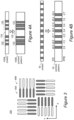
- FIGS 4A and 4B are high-level schematic illustrations of segmented periodic structures 100B, 92 - with and without missing element(s) 125, respectively, according to some embodiments of the invention.
- Segmented periodic structures 100B, 92 are illustrated as designed on the mask and as printed on the wafer, with 10m ⁇ coma as a non-limiting example for an asymmetric aberration.
- ⁇ CD 3.8 nm
- measured mis-registration 8.15 nm.
- Such enhancement may be used to provide a sensitive estimation of asymmetric aberrations.
- Figure 5 is a high-level flowchart illustrating a method 200, according to some embodiments of the invention.
- the method stages may be carried out with respect to metrology targets 100 described above, which may optionally be configured to implement method 200.
- Method 200 may be at least partially implemented by at least one computer processor, e.g., in a metrology module.
- Certain embodiments comprise computer program products comprising a computer readable storage medium having computer readable program embodied therewith and configured to carry out the relevant stages of method 200.
- Certain embodiments comprise target design files of respective targets designed by embodiments of method 200 as well as metrology measurements of targets 100 and/or metrology measurements that are carried out using stages of method 200.
- Method 200 may comprise the following stages, irrespective of their order.
- Method 200 comprises designing a metrology target to comprise at least two segmented periodic structures having a same coarse pitch, a same line to space (L:S) ratio of 1:1 and are segmented into fine elements at a same fine pitch (stage 210 ), and configuring the segmented periodic structures to differ from each other in their segment configurations (stage 212 ), e.g., with one of the segmented periodic structures lacking at least one of its corresponding fine elements (stage 214 ), e.g., the lacking fine element(s) may be central with respect to the corresponding elements of the corresponding periodic structure; and/or in that one thereof comprises two groups of the fine elements which are separated from each other by an integer number of of the fine pitch.
- Method 200 may comprise designing at least two pairs of segmented periodic structures, each pair having a different fine pitch (stage 216 ).
- Method 200 may further comprise producing and using the designed metrology target to derive an aberration estimation from measurements of the at least two segmented periodic structures (stage 220 ). Certain embodiments further comprise applying learning stage(s) such as using simulation(s) or actual measurement(s), e.g., to provide initial approximations or to implement machine learning algorithms to enhance the derivation of the aberration estimations (stage 222 ).
- learning stage(s) such as using simulation(s) or actual measurement(s), e.g., to provide initial approximations or to implement machine learning algorithms to enhance the derivation of the aberration estimations (stage 222 ).
- method 200 may further comprise adding at least one periodic structure to the at least two segmented periodic structures (stage 230 ), and configuring the at least one periodic structure to provide an overlay estimation from measurements thereof with respect to at least one of the segmented periodic structures (stage 232 ).
- Method 200 may further comprise selecting the fine pitch, or multiple fine pitches in case of multiple pairs of segmented periodic structures, to correspond to given device pitch(es) (stage 240 ).
- segmented periodic structures 100A, 100B with the same coarse pitch, 1:1 L:S ratio and same fine pitch, which differ from each other in missing element(s), or gap(s) 125 may be implemented using target structures disclosed in U.S. Patent Application Publication No. 2019250504 teaching the addition of sub-resolved assist features at a same periodicity as, and in continuation of, periodic structure(s) in the target's mask design, with the sub-resolved assist features having a CD that is smaller than a corresponding printability threshold.
- the measurement of such targets may provide an estimation of the scanner asymmetric aberrations.
- Disclosed embodiments provide solutions that handle the significant impact of asymmetric scanner aberrations on the overlay error budget. Since the effects of asymmetric aberration on different structures may be different, the pattern placement shifts of printed targets may be different, which makes their measurement in the prior art complicated (e.g., using a complicated calibration procedure per scanner ⁇ target) as they relate to both the device shifts due to the aberrations and to the difference between metrology target shifts with respect to the device design, as discussed in U.S. Patent Application Publication No. 2019250504 .
- disclosed embodiments provide a simpler solution for estimating asymmetric aberrations using target structures which have the same segmentation pitch as the device pitch (so that they are affected by the same aberrations as the devices are) but have an additional mechanism to provide estimations of the effects of the aberrations and their impact of the overlay measurement).
- disclosed embodiments provide imaging-based estimations of asymmetric aberration impact, that may be designed specifically per customer periodic structures, on-product scanner aberration impact measurement procedures, targets which are highly sensitive to scanner asymmetric aberrations, targets that can measure overlay and aberrations at the same time, as well as targets and measurement methods which provide measurements of the aberration equivalents per device design.
- These computer program instructions may also be stored in a computer readable medium that can direct a computer, other programmable data processing apparatus, or other devices to function in a particular manner, such that the instructions stored in the computer readable medium produce an article of manufacture including instructions which implement the function/act specified in the flowchart and/or portion diagram or portions thereof.
- the computer program instructions may also be loaded onto a computer, other programmable data processing apparatus, or other devices to cause a series of operational steps to be performed on the computer, other programmable apparatus or other devices to produce a computer implemented process such that the instructions which execute on the computer or other programmable apparatus provide processes for implementing the functions/acts specified in the flowchart and/or portion diagram or portions thereof.
- each portion in the flowchart or portion diagrams may represent a module, segment, or portion of code, which comprises one or more executable instructions for implementing the specified logical function(s).
- the functions noted in the portion may occur out of the order noted in the figures. For example, two portions shown in succession may, in fact, be executed substantially concurrently, or the portions may sometimes be executed in the reverse order, depending upon the functionality involved.
- each portion of the portion diagrams and/or flowchart illustration, and combinations of portions in the portion diagrams and/or flowchart illustration can be implemented by special purpose hardware-based systems that perform the specified functions or acts, or combinations of special purpose hardware and computer instructions.
Landscapes
- Physics & Mathematics (AREA)
- General Physics & Mathematics (AREA)
- Health & Medical Sciences (AREA)
- Life Sciences & Earth Sciences (AREA)
- Chemical & Material Sciences (AREA)
- Analytical Chemistry (AREA)
- Biochemistry (AREA)
- General Health & Medical Sciences (AREA)
- Immunology (AREA)
- Pathology (AREA)
- Exposure And Positioning Against Photoresist Photosensitive Materials (AREA)
Claims (15)
- Messtechnikziel (100), das mindestens zwei segmentierte periodische Strukturen (100A), (100B) umfasst, die eine gleiche Grobteilung, ein gleiches Linie-Raum-Verhältnis (L:S) von 1:1 aufweisen und die mit einer gleichen Feinteilung in Feinelemente (120) segmentiert sind, dadurch gekennzeichnet, dass sich die segmentierten periodischen Strukturen dadurch voneinander unterscheiden, dass eine davon:mindestens eines ihrer entsprechenden Feinelemente unter Beibehaltung des gleichen L:S-Verhältnisses fehlt; oderzwei Gruppen (122) der Feinelemente (120) umfasst, die durch ein ganzzahliges Vielfaches der Feinteilung unter Beibehaltung des gleichen L:S-Verhältnisses voneinander getrennt sind.
- Messtechnikziel nach Anspruch 1, wobei das mindestens eine fehlende Feinelement in Bezug auf Elemente der entsprechenden periodischen Struktur zentral liegt.
- Messtechnikziel nach einem der Ansprüche 1-2, wobei die segmentierten periodischen Strukturen (100A) (100B) in einer gleichen Zielschicht liegen.
- Messtechnikziel nach einem der Ansprüche 1-3, wobei die segmentierten periodischen Strukturen (100A) (100B) mindestens zwei Paare von segmentierten periodischen Strukturen umfassen, wobei jedes Paar eine unterschiedliche Feinteilung aufweist.
- Messtechnikziel nach einem der Ansprüche 1-4, ferner umfassend mindestens eine periodische Struktur, die zum Ergeben von Überlagerungsmessungen in Bezug auf mindestens eine der segmentierten periodischen Strukturen konfiguriert ist.
- Zielentwurfsdatei des Messtechnikziels nach einem der Ansprüche 1-5.
- Verfahren zum Erhalten von Messtechnik-Messdaten durch Messen des Messtechnikziels nach einem der Ansprüche 1-5.
- Verfahren (200) umfassend:Entwerfen eines Messtechnikziels, das mindestens zwei segmentierte periodische Strukturen umfasst, die eine gleiche Grobteilung, ein gleiches Linie-Raum-Verhältnis (L:S) von 1:1 aufweisen und die mit einer gleichen Feinteilung in Feinelemente segmentiert sind (210), undKonfigurieren der segmentierten periodischen Strukturen derart, dass sie sich dadurch voneinander unterscheiden, das eine davon mindestens eines ihrer entsprechenden Feinelemente unter Beibehaltung des gleichen L:S-Verhältnisses fehlt, oder dadurch, dass eine davon zwei Gruppen der Feinelemente umfasst, die durch ein ganzzahliges Vielfaches der Feinteilung unter Beibehaltung des gleichen L:S-Verhältnisses voneinander getrennt sind (212, 214),wobei das Entwerfen und/oder das Konfigurieren durch mindestens einen Computerprozessor durchgeführt wird.
- Verfahren nach Anspruch 8, wobei das mindestens eine fehlende Feinelement in Bezug auf Elemente der entsprechenden periodischen Struktur zentral liegt.
- Verfahren, umfassend die folgenden Schritte:Produzieren eines gemäß dem Verfahren nach Anspruch 8 oder 9 entworfenen und konfigurierten Messtechnikziels mit einem Lithografiescanner,Erhalten von Messdaten durch Messen der mindestens zwei segmentierten periodischen Strukturen des produzierten Messtechnikziels undVerwenden der Messdaten zum Ableiten einer Schätzung einer Aberration des Lithografiescanners (220).
- Verfahren nach Anspruch 8, ferner umfassend Hinzufügen mindestens einer periodischen Struktur zu den mindestens zwei segmentierten periodischen Strukturen (230) und Konfigurieren der mindestens einen periodischen Struktur zum Bereitstellen einer Überlagerungsschätzung aus Messungen davon in Bezug auf mindestens eine der segmentierten periodischen Strukturen (232) .
- Verfahren nach Anspruch 8, ferner umfassend Auswählen der Feinteilung, sodass sie einer vorgegebenen Vorrichtungsteilung entspricht (240).
- Verfahren nach Anspruch 8:ferner umfassend Entwerfen mindestens zweier Paare segmentierter periodischer Strukturen, wobei jedes Paar eine unterschiedliche Feinteilung aufweist; undferner umfassend Auswählen der Feinteilungen, sodass sie vorgegebenen Vorrichtungsteilungen entsprechen.
- Computerprogrammprodukt, umfassend ein nichtflüchtiges computerlesbares Speichermedium, das ein damit integriertes computerlesbares Programm aufweist, wobei das computerlesbare Programm zum Ausführen des Verfahrens nach Anspruch 10 konfiguriert ist.
- Messtechnikmodul, umfassend das Computerprogrammprodukt nach Anspruch 14.
Applications Claiming Priority (1)
| Application Number | Priority Date | Filing Date | Title |
|---|---|---|---|
| PCT/US2018/058068 WO2020091733A1 (en) | 2018-10-30 | 2018-10-30 | Estimation of asymmetric aberrations |
Publications (3)
| Publication Number | Publication Date |
|---|---|
| EP3853665A1 EP3853665A1 (de) | 2021-07-28 |
| EP3853665A4 EP3853665A4 (de) | 2022-05-18 |
| EP3853665B1 true EP3853665B1 (de) | 2023-12-20 |
Family
ID=70325248
Family Applications (1)
| Application Number | Title | Priority Date | Filing Date |
|---|---|---|---|
| EP18938833.3A Active EP3853665B1 (de) | 2018-10-30 | 2018-10-30 | Schätzung von asymmetrischen aberrationen |
Country Status (7)
| Country | Link |
|---|---|
| US (1) | US10824082B2 (de) |
| EP (1) | EP3853665B1 (de) |
| JP (1) | JP7225388B2 (de) |
| KR (1) | KR102381168B1 (de) |
| CN (1) | CN112789557A (de) |
| SG (1) | SG11202103847QA (de) |
| WO (1) | WO2020091733A1 (de) |
Families Citing this family (2)
| Publication number | Priority date | Publication date | Assignee | Title |
|---|---|---|---|---|
| US11971664B2 (en) * | 2018-07-30 | 2024-04-30 | Kla-Tencor Corporation | Reducing device overlay errors |
| US12044982B2 (en) * | 2021-12-02 | 2024-07-23 | Micron Technology, Inc. | Apparatuses and methods for diffraction base overlay measurements |
Family Cites Families (14)
| Publication number | Priority date | Publication date | Assignee | Title |
|---|---|---|---|---|
| US5790254A (en) * | 1994-12-20 | 1998-08-04 | International Business Machines Corporation | Monitoring of minimum features on a substrate |
| JP5180419B2 (ja) * | 2000-08-30 | 2013-04-10 | ケーエルエー−テンカー・コーポレーション | 重ね合わせマーク、重ね合わせマークの設計方法および重ね合わせ測定の方法 |
| EP1400854A3 (de) * | 2002-09-20 | 2009-07-08 | ASML Netherlands B.V. | Systeme und Verfahren zum Ausrichten für Lithographische Systeme |
| US7608468B1 (en) * | 2003-07-02 | 2009-10-27 | Kla-Tencor Technologies, Corp. | Apparatus and methods for determining overlay and uses of same |
| EP1709490B1 (de) * | 2003-12-19 | 2010-08-04 | International Business Machines Corporation | Differentielle metrologie für kritische abmessung und überlagerung |
| US7456966B2 (en) * | 2004-01-19 | 2008-11-25 | International Business Machines Corporation | Alignment mark system and method to improve wafer alignment search range |
| US20080013090A1 (en) * | 2006-03-29 | 2008-01-17 | Nikon Corporation | Measurement method, measurement unit, processing unit, pattern forming method , and device manufacturing method |
| US9709903B2 (en) | 2011-11-01 | 2017-07-18 | Kla-Tencor Corporation | Overlay target geometry for measuring multiple pitches |
| WO2014074873A1 (en) * | 2012-11-09 | 2014-05-15 | Kla-Tencor Corporation | Reducing algorithmic inaccuracy in scatterometry overlay metrology |
| TWI621190B (zh) * | 2013-06-19 | 2018-04-11 | 克萊譚克公司 | 併合成像及散射測量靶 |
| NL2013838A (en) * | 2013-12-17 | 2015-06-18 | Asml Netherlands Bv | Inspection method, lithographic apparatus, mask and substrate. |
| KR102729959B1 (ko) | 2015-04-21 | 2024-11-13 | 케이엘에이 코포레이션 | 기울어진 디바이스 설계를 위한 계측 타겟 설계 |
| WO2017176314A1 (en) * | 2016-04-04 | 2017-10-12 | Kla-Tencor Corporation | Process compatibility improvement by fill factor modulation |
| WO2019083560A1 (en) | 2017-10-23 | 2019-05-02 | Kla-Tencor Corporation | REDUCTION OR ELIMINATION OF PATTERN PLACEMENT ERROR IN METROLOGY MEASUREMENTS |
-
2018
- 2018-10-30 KR KR1020217016047A patent/KR102381168B1/ko active Active
- 2018-10-30 US US16/305,629 patent/US10824082B2/en active Active
- 2018-10-30 JP JP2021520572A patent/JP7225388B2/ja active Active
- 2018-10-30 EP EP18938833.3A patent/EP3853665B1/de active Active
- 2018-10-30 CN CN201880098352.1A patent/CN112789557A/zh active Pending
- 2018-10-30 WO PCT/US2018/058068 patent/WO2020091733A1/en not_active Ceased
- 2018-10-30 SG SG11202103847QA patent/SG11202103847QA/en unknown
Also Published As
| Publication number | Publication date |
|---|---|
| JP7225388B2 (ja) | 2023-02-20 |
| KR20210069116A (ko) | 2021-06-10 |
| EP3853665A1 (de) | 2021-07-28 |
| CN112789557A (zh) | 2021-05-11 |
| EP3853665A4 (de) | 2022-05-18 |
| SG11202103847QA (en) | 2021-05-28 |
| US10824082B2 (en) | 2020-11-03 |
| KR102381168B1 (ko) | 2022-03-30 |
| JP2021535445A (ja) | 2021-12-16 |
| WO2020091733A1 (en) | 2020-05-07 |
| US20200133135A1 (en) | 2020-04-30 |
Similar Documents
| Publication | Publication Date | Title |
|---|---|---|
| TWI798248B (zh) | 在計量量測中之機器學習 | |
| CN109844647B (zh) | 基于衍射的聚焦度量 | |
| US10685165B2 (en) | Metrology using overlay and yield critical patterns | |
| US11054752B2 (en) | Device metrology targets and methods | |
| JP7011592B2 (ja) | スキャトロメトリ計測におけるプロセス変動の根本原因の解析 | |
| US10228320B1 (en) | Achieving a small pattern placement error in metrology targets | |
| US12013634B2 (en) | Reduction or elimination of pattern placement error in metrology measurements | |
| US20150233705A1 (en) | Reducing algorithmic inaccuracy in scatterometry overlay metrology | |
| US8230369B2 (en) | Simulation method and simulation program | |
| US10824082B2 (en) | Estimation of asymmetric aberrations | |
| US7930654B2 (en) | System and method of correcting errors in SEM-measurements | |
| US11971664B2 (en) | Reducing device overlay errors | |
| KR20210081434A (ko) | 단일 셀 그레이 산란계측 오버레이 타겟 및 다양한 조명 파라미터를 사용한 이들의 측정 | |
| EP3639166B1 (de) | Retikel optimierungsalgorithmen und optimales zieldesign | |
| TWI799654B (zh) | 度量衡目標,半導體度量衡的方法,電腦程式產品,及度量衡模組 |
Legal Events
| Date | Code | Title | Description |
|---|---|---|---|
| STAA | Information on the status of an ep patent application or granted ep patent |
Free format text: STATUS: THE INTERNATIONAL PUBLICATION HAS BEEN MADE |
|
| PUAI | Public reference made under article 153(3) epc to a published international application that has entered the european phase |
Free format text: ORIGINAL CODE: 0009012 |
|
| STAA | Information on the status of an ep patent application or granted ep patent |
Free format text: STATUS: REQUEST FOR EXAMINATION WAS MADE |
|
| 17P | Request for examination filed |
Effective date: 20210421 |
|
| AK | Designated contracting states |
Kind code of ref document: A1 Designated state(s): AL AT BE BG CH CY CZ DE DK EE ES FI FR GB GR HR HU IE IS IT LI LT LU LV MC MK MT NL NO PL PT RO RS SE SI SK SM TR |
|
| DAV | Request for validation of the european patent (deleted) | ||
| DAX | Request for extension of the european patent (deleted) | ||
| A4 | Supplementary search report drawn up and despatched |
Effective date: 20220419 |
|
| RIC1 | Information provided on ipc code assigned before grant |
Ipc: H01L 21/66 20060101ALI20220411BHEP Ipc: G03F 7/20 20060101AFI20220411BHEP |
|
| GRAP | Despatch of communication of intention to grant a patent |
Free format text: ORIGINAL CODE: EPIDOSNIGR1 |
|
| STAA | Information on the status of an ep patent application or granted ep patent |
Free format text: STATUS: GRANT OF PATENT IS INTENDED |
|
| P01 | Opt-out of the competence of the unified patent court (upc) registered |
Effective date: 20230526 |
|
| INTG | Intention to grant announced |
Effective date: 20230710 |
|
| GRAS | Grant fee paid |
Free format text: ORIGINAL CODE: EPIDOSNIGR3 |
|
| GRAA | (expected) grant |
Free format text: ORIGINAL CODE: 0009210 |
|
| STAA | Information on the status of an ep patent application or granted ep patent |
Free format text: STATUS: THE PATENT HAS BEEN GRANTED |
|
| AK | Designated contracting states |
Kind code of ref document: B1 Designated state(s): AL AT BE BG CH CY CZ DE DK EE ES FI FR GB GR HR HU IE IS IT LI LT LU LV MC MK MT NL NO PL PT RO RS SE SI SK SM TR |
|
| REG | Reference to a national code |
Ref country code: GB Ref legal event code: FG4D |
|
| REG | Reference to a national code |
Ref country code: DE Ref legal event code: R096 Ref document number: 602018063082 Country of ref document: DE |
|
| REG | Reference to a national code |
Ref country code: CH Ref legal event code: EP |
|
| REG | Reference to a national code |
Ref country code: NL Ref legal event code: FP |
|
| REG | Reference to a national code |
Ref country code: IE Ref legal event code: FG4D |
|
| PG25 | Lapsed in a contracting state [announced via postgrant information from national office to epo] |
Ref country code: GR Free format text: LAPSE BECAUSE OF FAILURE TO SUBMIT A TRANSLATION OF THE DESCRIPTION OR TO PAY THE FEE WITHIN THE PRESCRIBED TIME-LIMIT Effective date: 20240321 |
|
| REG | Reference to a national code |
Ref country code: LT Ref legal event code: MG9D |
|
| PG25 | Lapsed in a contracting state [announced via postgrant information from national office to epo] |
Ref country code: LT Free format text: LAPSE BECAUSE OF FAILURE TO SUBMIT A TRANSLATION OF THE DESCRIPTION OR TO PAY THE FEE WITHIN THE PRESCRIBED TIME-LIMIT Effective date: 20231220 |
|
| PG25 | Lapsed in a contracting state [announced via postgrant information from national office to epo] |
Ref country code: ES Free format text: LAPSE BECAUSE OF FAILURE TO SUBMIT A TRANSLATION OF THE DESCRIPTION OR TO PAY THE FEE WITHIN THE PRESCRIBED TIME-LIMIT Effective date: 20231220 |
|
| PG25 | Lapsed in a contracting state [announced via postgrant information from national office to epo] |
Ref country code: LT Free format text: LAPSE BECAUSE OF FAILURE TO SUBMIT A TRANSLATION OF THE DESCRIPTION OR TO PAY THE FEE WITHIN THE PRESCRIBED TIME-LIMIT Effective date: 20231220 Ref country code: GR Free format text: LAPSE BECAUSE OF FAILURE TO SUBMIT A TRANSLATION OF THE DESCRIPTION OR TO PAY THE FEE WITHIN THE PRESCRIBED TIME-LIMIT Effective date: 20240321 Ref country code: FI Free format text: LAPSE BECAUSE OF FAILURE TO SUBMIT A TRANSLATION OF THE DESCRIPTION OR TO PAY THE FEE WITHIN THE PRESCRIBED TIME-LIMIT Effective date: 20231220 Ref country code: ES Free format text: LAPSE BECAUSE OF FAILURE TO SUBMIT A TRANSLATION OF THE DESCRIPTION OR TO PAY THE FEE WITHIN THE PRESCRIBED TIME-LIMIT Effective date: 20231220 Ref country code: BG Free format text: LAPSE BECAUSE OF FAILURE TO SUBMIT A TRANSLATION OF THE DESCRIPTION OR TO PAY THE FEE WITHIN THE PRESCRIBED TIME-LIMIT Effective date: 20240320 |
|
| REG | Reference to a national code |
Ref country code: AT Ref legal event code: MK05 Ref document number: 1642976 Country of ref document: AT Kind code of ref document: T Effective date: 20231220 |
|
| PG25 | Lapsed in a contracting state [announced via postgrant information from national office to epo] |
Ref country code: SE Free format text: LAPSE BECAUSE OF FAILURE TO SUBMIT A TRANSLATION OF THE DESCRIPTION OR TO PAY THE FEE WITHIN THE PRESCRIBED TIME-LIMIT Effective date: 20231220 Ref country code: RS Free format text: LAPSE BECAUSE OF FAILURE TO SUBMIT A TRANSLATION OF THE DESCRIPTION OR TO PAY THE FEE WITHIN THE PRESCRIBED TIME-LIMIT Effective date: 20231220 Ref country code: NO Free format text: LAPSE BECAUSE OF FAILURE TO SUBMIT A TRANSLATION OF THE DESCRIPTION OR TO PAY THE FEE WITHIN THE PRESCRIBED TIME-LIMIT Effective date: 20240320 Ref country code: LV Free format text: LAPSE BECAUSE OF FAILURE TO SUBMIT A TRANSLATION OF THE DESCRIPTION OR TO PAY THE FEE WITHIN THE PRESCRIBED TIME-LIMIT Effective date: 20231220 Ref country code: HR Free format text: LAPSE BECAUSE OF FAILURE TO SUBMIT A TRANSLATION OF THE DESCRIPTION OR TO PAY THE FEE WITHIN THE PRESCRIBED TIME-LIMIT Effective date: 20231220 |
|
| PG25 | Lapsed in a contracting state [announced via postgrant information from national office to epo] |
Ref country code: IS Free format text: LAPSE BECAUSE OF FAILURE TO SUBMIT A TRANSLATION OF THE DESCRIPTION OR TO PAY THE FEE WITHIN THE PRESCRIBED TIME-LIMIT Effective date: 20240420 |
|
| PG25 | Lapsed in a contracting state [announced via postgrant information from national office to epo] |
Ref country code: CZ Free format text: LAPSE BECAUSE OF FAILURE TO SUBMIT A TRANSLATION OF THE DESCRIPTION OR TO PAY THE FEE WITHIN THE PRESCRIBED TIME-LIMIT Effective date: 20231220 Ref country code: AT Free format text: LAPSE BECAUSE OF FAILURE TO SUBMIT A TRANSLATION OF THE DESCRIPTION OR TO PAY THE FEE WITHIN THE PRESCRIBED TIME-LIMIT Effective date: 20231220 |
|
| PG25 | Lapsed in a contracting state [announced via postgrant information from national office to epo] |
Ref country code: SK Free format text: LAPSE BECAUSE OF FAILURE TO SUBMIT A TRANSLATION OF THE DESCRIPTION OR TO PAY THE FEE WITHIN THE PRESCRIBED TIME-LIMIT Effective date: 20231220 |
|
| PG25 | Lapsed in a contracting state [announced via postgrant information from national office to epo] |
Ref country code: SM Free format text: LAPSE BECAUSE OF FAILURE TO SUBMIT A TRANSLATION OF THE DESCRIPTION OR TO PAY THE FEE WITHIN THE PRESCRIBED TIME-LIMIT Effective date: 20231220 Ref country code: SK Free format text: LAPSE BECAUSE OF FAILURE TO SUBMIT A TRANSLATION OF THE DESCRIPTION OR TO PAY THE FEE WITHIN THE PRESCRIBED TIME-LIMIT Effective date: 20231220 Ref country code: RO Free format text: LAPSE BECAUSE OF FAILURE TO SUBMIT A TRANSLATION OF THE DESCRIPTION OR TO PAY THE FEE WITHIN THE PRESCRIBED TIME-LIMIT Effective date: 20231220 Ref country code: IT Free format text: LAPSE BECAUSE OF FAILURE TO SUBMIT A TRANSLATION OF THE DESCRIPTION OR TO PAY THE FEE WITHIN THE PRESCRIBED TIME-LIMIT Effective date: 20231220 Ref country code: IS Free format text: LAPSE BECAUSE OF FAILURE TO SUBMIT A TRANSLATION OF THE DESCRIPTION OR TO PAY THE FEE WITHIN THE PRESCRIBED TIME-LIMIT Effective date: 20240420 Ref country code: EE Free format text: LAPSE BECAUSE OF FAILURE TO SUBMIT A TRANSLATION OF THE DESCRIPTION OR TO PAY THE FEE WITHIN THE PRESCRIBED TIME-LIMIT Effective date: 20231220 Ref country code: CZ Free format text: LAPSE BECAUSE OF FAILURE TO SUBMIT A TRANSLATION OF THE DESCRIPTION OR TO PAY THE FEE WITHIN THE PRESCRIBED TIME-LIMIT Effective date: 20231220 Ref country code: AT Free format text: LAPSE BECAUSE OF FAILURE TO SUBMIT A TRANSLATION OF THE DESCRIPTION OR TO PAY THE FEE WITHIN THE PRESCRIBED TIME-LIMIT Effective date: 20231220 |
|
| PG25 | Lapsed in a contracting state [announced via postgrant information from national office to epo] |
Ref country code: PL Free format text: LAPSE BECAUSE OF FAILURE TO SUBMIT A TRANSLATION OF THE DESCRIPTION OR TO PAY THE FEE WITHIN THE PRESCRIBED TIME-LIMIT Effective date: 20231220 Ref country code: PT Free format text: LAPSE BECAUSE OF FAILURE TO SUBMIT A TRANSLATION OF THE DESCRIPTION OR TO PAY THE FEE WITHIN THE PRESCRIBED TIME-LIMIT Effective date: 20240422 |
|
| PG25 | Lapsed in a contracting state [announced via postgrant information from national office to epo] |
Ref country code: PT Free format text: LAPSE BECAUSE OF FAILURE TO SUBMIT A TRANSLATION OF THE DESCRIPTION OR TO PAY THE FEE WITHIN THE PRESCRIBED TIME-LIMIT Effective date: 20240422 Ref country code: PL Free format text: LAPSE BECAUSE OF FAILURE TO SUBMIT A TRANSLATION OF THE DESCRIPTION OR TO PAY THE FEE WITHIN THE PRESCRIBED TIME-LIMIT Effective date: 20231220 |
|
| REG | Reference to a national code |
Ref country code: DE Ref legal event code: R097 Ref document number: 602018063082 Country of ref document: DE |
|
| PG25 | Lapsed in a contracting state [announced via postgrant information from national office to epo] |
Ref country code: DK Free format text: LAPSE BECAUSE OF FAILURE TO SUBMIT A TRANSLATION OF THE DESCRIPTION OR TO PAY THE FEE WITHIN THE PRESCRIBED TIME-LIMIT Effective date: 20231220 |
|
| PLBE | No opposition filed within time limit |
Free format text: ORIGINAL CODE: 0009261 |
|
| STAA | Information on the status of an ep patent application or granted ep patent |
Free format text: STATUS: NO OPPOSITION FILED WITHIN TIME LIMIT |
|
| PG25 | Lapsed in a contracting state [announced via postgrant information from national office to epo] |
Ref country code: SI Free format text: LAPSE BECAUSE OF FAILURE TO SUBMIT A TRANSLATION OF THE DESCRIPTION OR TO PAY THE FEE WITHIN THE PRESCRIBED TIME-LIMIT Effective date: 20231220 |
|
| PG25 | Lapsed in a contracting state [announced via postgrant information from national office to epo] |
Ref country code: SI Free format text: LAPSE BECAUSE OF FAILURE TO SUBMIT A TRANSLATION OF THE DESCRIPTION OR TO PAY THE FEE WITHIN THE PRESCRIBED TIME-LIMIT Effective date: 20231220 Ref country code: DK Free format text: LAPSE BECAUSE OF FAILURE TO SUBMIT A TRANSLATION OF THE DESCRIPTION OR TO PAY THE FEE WITHIN THE PRESCRIBED TIME-LIMIT Effective date: 20231220 |
|
| 26N | No opposition filed |
Effective date: 20240923 |
|
| REG | Reference to a national code |
Ref country code: CH Ref legal event code: PL |
|
| GBPC | Gb: european patent ceased through non-payment of renewal fee |
Effective date: 20241030 |
|
| PG25 | Lapsed in a contracting state [announced via postgrant information from national office to epo] |
Ref country code: MC Free format text: LAPSE BECAUSE OF FAILURE TO SUBMIT A TRANSLATION OF THE DESCRIPTION OR TO PAY THE FEE WITHIN THE PRESCRIBED TIME-LIMIT Effective date: 20231220 |
|
| PG25 | Lapsed in a contracting state [announced via postgrant information from national office to epo] |
Ref country code: GB Free format text: LAPSE BECAUSE OF NON-PAYMENT OF DUE FEES Effective date: 20241030 |
|
| PG25 | Lapsed in a contracting state [announced via postgrant information from national office to epo] |
Ref country code: BE Free format text: LAPSE BECAUSE OF NON-PAYMENT OF DUE FEES Effective date: 20241031 Ref country code: LU Free format text: LAPSE BECAUSE OF NON-PAYMENT OF DUE FEES Effective date: 20241030 |
|
| PG25 | Lapsed in a contracting state [announced via postgrant information from national office to epo] |
Ref country code: FR Free format text: LAPSE BECAUSE OF NON-PAYMENT OF DUE FEES Effective date: 20241031 |
|
| PG25 | Lapsed in a contracting state [announced via postgrant information from national office to epo] |
Ref country code: CH Free format text: LAPSE BECAUSE OF NON-PAYMENT OF DUE FEES Effective date: 20241031 |
|
| REG | Reference to a national code |
Ref country code: BE Ref legal event code: MM Effective date: 20241031 |
|
| PG25 | Lapsed in a contracting state [announced via postgrant information from national office to epo] |
Ref country code: IE Free format text: LAPSE BECAUSE OF NON-PAYMENT OF DUE FEES Effective date: 20241030 |
|
| PGFP | Annual fee paid to national office [announced via postgrant information from national office to epo] |
Ref country code: NL Payment date: 20251026 Year of fee payment: 8 |
|
| PGFP | Annual fee paid to national office [announced via postgrant information from national office to epo] |
Ref country code: DE Payment date: 20251029 Year of fee payment: 8 |
|
| PG25 | Lapsed in a contracting state [announced via postgrant information from national office to epo] |
Ref country code: HU Free format text: LAPSE BECAUSE OF FAILURE TO SUBMIT A TRANSLATION OF THE DESCRIPTION OR TO PAY THE FEE WITHIN THE PRESCRIBED TIME-LIMIT; INVALID AB INITIO Effective date: 20181030 |
|
| PG25 | Lapsed in a contracting state [announced via postgrant information from national office to epo] |
Ref country code: CY Free format text: LAPSE BECAUSE OF FAILURE TO SUBMIT A TRANSLATION OF THE DESCRIPTION OR TO PAY THE FEE WITHIN THE PRESCRIBED TIME-LIMIT; INVALID AB INITIO Effective date: 20181030 |