EP3852155A1 - Light emitting element, manufacturing method thereof, and composition including the same - Google Patents
Light emitting element, manufacturing method thereof, and composition including the same Download PDFInfo
- Publication number
- EP3852155A1 EP3852155A1 EP20196980.5A EP20196980A EP3852155A1 EP 3852155 A1 EP3852155 A1 EP 3852155A1 EP 20196980 A EP20196980 A EP 20196980A EP 3852155 A1 EP3852155 A1 EP 3852155A1
- Authority
- EP
- European Patent Office
- Prior art keywords
- group
- light emitting
- emitting element
- polymer chain
- semiconductor layer
- Prior art date
- Legal status (The legal status is an assumption and is not a legal conclusion. Google has not performed a legal analysis and makes no representation as to the accuracy of the status listed.)
- Granted
Links
Images




Classifications
-
- H—ELECTRICITY
- H10—SEMICONDUCTOR DEVICES; ELECTRIC SOLID-STATE DEVICES NOT OTHERWISE PROVIDED FOR
- H10H—INORGANIC LIGHT-EMITTING SEMICONDUCTOR DEVICES HAVING POTENTIAL BARRIERS
- H10H20/00—Individual inorganic light-emitting semiconductor devices having potential barriers, e.g. light-emitting diodes [LED]
- H10H20/80—Constructional details
- H10H20/81—Bodies
- H10H20/813—Bodies having a plurality of light-emitting regions, e.g. multi-junction LEDs or light-emitting devices having photoluminescent regions within the bodies
-
- H—ELECTRICITY
- H10—SEMICONDUCTOR DEVICES; ELECTRIC SOLID-STATE DEVICES NOT OTHERWISE PROVIDED FOR
- H10H—INORGANIC LIGHT-EMITTING SEMICONDUCTOR DEVICES HAVING POTENTIAL BARRIERS
- H10H20/00—Individual inorganic light-emitting semiconductor devices having potential barriers, e.g. light-emitting diodes [LED]
- H10H20/80—Constructional details
- H10H20/85—Packages
- H10H20/852—Encapsulations
- H10H20/854—Encapsulations characterised by their material, e.g. epoxy or silicone resins
-
- C—CHEMISTRY; METALLURGY
- C08—ORGANIC MACROMOLECULAR COMPOUNDS; THEIR PREPARATION OR CHEMICAL WORKING-UP; COMPOSITIONS BASED THEREON
- C08G—MACROMOLECULAR COMPOUNDS OBTAINED OTHERWISE THAN BY REACTIONS ONLY INVOLVING UNSATURATED CARBON-TO-CARBON BONDS
- C08G61/00—Macromolecular compounds obtained by reactions forming a carbon-to-carbon link in the main chain of the macromolecule
- C08G61/02—Macromolecular compounds containing only carbon atoms in the main chain of the macromolecule, e.g. polyxylylenes
- C08G61/10—Macromolecular compounds containing only carbon atoms in the main chain of the macromolecule, e.g. polyxylylenes only aromatic carbon atoms, e.g. polyphenylenes
-
- C—CHEMISTRY; METALLURGY
- C08—ORGANIC MACROMOLECULAR COMPOUNDS; THEIR PREPARATION OR CHEMICAL WORKING-UP; COMPOSITIONS BASED THEREON
- C08L—COMPOSITIONS OF MACROMOLECULAR COMPOUNDS
- C08L47/00—Compositions of homopolymers or copolymers of compounds having one or more unsaturated aliphatic radicals, at least one having two or more carbon-to-carbon double bonds; Compositions of derivatives of such polymers
-
- C—CHEMISTRY; METALLURGY
- C08—ORGANIC MACROMOLECULAR COMPOUNDS; THEIR PREPARATION OR CHEMICAL WORKING-UP; COMPOSITIONS BASED THEREON
- C08L—COMPOSITIONS OF MACROMOLECULAR COMPOUNDS
- C08L65/00—Compositions of macromolecular compounds obtained by reactions forming a carbon-to-carbon link in the main chain; Compositions of derivatives of such polymers
- C08L65/02—Polyphenylenes
-
- C—CHEMISTRY; METALLURGY
- C09—DYES; PAINTS; POLISHES; NATURAL RESINS; ADHESIVES; COMPOSITIONS NOT OTHERWISE PROVIDED FOR; APPLICATIONS OF MATERIALS NOT OTHERWISE PROVIDED FOR
- C09D—COATING COMPOSITIONS, e.g. PAINTS, VARNISHES OR LACQUERS; FILLING PASTES; CHEMICAL PAINT OR INK REMOVERS; INKS; CORRECTING FLUIDS; WOODSTAINS; PASTES OR SOLIDS FOR COLOURING OR PRINTING; USE OF MATERIALS THEREFOR
- C09D165/00—Coating compositions based on macromolecular compounds obtained by reactions forming a carbon-to-carbon link in the main chain; Coating compositions based on derivatives of such polymers
-
- H—ELECTRICITY
- H10—SEMICONDUCTOR DEVICES; ELECTRIC SOLID-STATE DEVICES NOT OTHERWISE PROVIDED FOR
- H10H—INORGANIC LIGHT-EMITTING SEMICONDUCTOR DEVICES HAVING POTENTIAL BARRIERS
- H10H20/00—Individual inorganic light-emitting semiconductor devices having potential barriers, e.g. light-emitting diodes [LED]
- H10H20/01—Manufacture or treatment
-
- H—ELECTRICITY
- H10—SEMICONDUCTOR DEVICES; ELECTRIC SOLID-STATE DEVICES NOT OTHERWISE PROVIDED FOR
- H10H—INORGANIC LIGHT-EMITTING SEMICONDUCTOR DEVICES HAVING POTENTIAL BARRIERS
- H10H20/00—Individual inorganic light-emitting semiconductor devices having potential barriers, e.g. light-emitting diodes [LED]
- H10H20/80—Constructional details
- H10H20/83—Electrodes
-
- H—ELECTRICITY
- H10—SEMICONDUCTOR DEVICES; ELECTRIC SOLID-STATE DEVICES NOT OTHERWISE PROVIDED FOR
- H10H—INORGANIC LIGHT-EMITTING SEMICONDUCTOR DEVICES HAVING POTENTIAL BARRIERS
- H10H20/00—Individual inorganic light-emitting semiconductor devices having potential barriers, e.g. light-emitting diodes [LED]
- H10H20/80—Constructional details
- H10H20/84—Coatings, e.g. passivation layers or antireflective coatings
-
- C—CHEMISTRY; METALLURGY
- C08—ORGANIC MACROMOLECULAR COMPOUNDS; THEIR PREPARATION OR CHEMICAL WORKING-UP; COMPOSITIONS BASED THEREON
- C08G—MACROMOLECULAR COMPOUNDS OBTAINED OTHERWISE THAN BY REACTIONS ONLY INVOLVING UNSATURATED CARBON-TO-CARBON BONDS
- C08G2261/00—Macromolecular compounds obtained by reactions forming a carbon-to-carbon link in the main chain of the macromolecule
- C08G2261/30—Monomer units or repeat units incorporating structural elements in the main chain
- C08G2261/31—Monomer units or repeat units incorporating structural elements in the main chain incorporating aromatic structural elements in the main chain
- C08G2261/314—Condensed aromatic systems, e.g. perylene, anthracene or pyrene
- C08G2261/3142—Condensed aromatic systems, e.g. perylene, anthracene or pyrene fluorene-based, e.g. fluorene, indenofluorene, or spirobifluorene
-
- H—ELECTRICITY
- H10—SEMICONDUCTOR DEVICES; ELECTRIC SOLID-STATE DEVICES NOT OTHERWISE PROVIDED FOR
- H10H—INORGANIC LIGHT-EMITTING SEMICONDUCTOR DEVICES HAVING POTENTIAL BARRIERS
- H10H20/00—Individual inorganic light-emitting semiconductor devices having potential barriers, e.g. light-emitting diodes [LED]
- H10H20/01—Manufacture or treatment
- H10H20/034—Manufacture or treatment of coatings
-
- H—ELECTRICITY
- H10—SEMICONDUCTOR DEVICES; ELECTRIC SOLID-STATE DEVICES NOT OTHERWISE PROVIDED FOR
- H10H—INORGANIC LIGHT-EMITTING SEMICONDUCTOR DEVICES HAVING POTENTIAL BARRIERS
- H10H20/00—Individual inorganic light-emitting semiconductor devices having potential barriers, e.g. light-emitting diodes [LED]
- H10H20/01—Manufacture or treatment
- H10H20/036—Manufacture or treatment of packages
- H10H20/0362—Manufacture or treatment of packages of encapsulations
-
- H—ELECTRICITY
- H10—SEMICONDUCTOR DEVICES; ELECTRIC SOLID-STATE DEVICES NOT OTHERWISE PROVIDED FOR
- H10W—GENERIC PACKAGES, INTERCONNECTIONS, CONNECTORS OR OTHER CONSTRUCTIONAL DETAILS OF DEVICES COVERED BY CLASS H10
- H10W72/00—Interconnections or connectors in packages
- H10W72/01—Manufacture or treatment
- H10W72/0198—Manufacture or treatment batch processes
Definitions
- Embodiments of the present disclosure relate to a light emitting element, a method of manufacturing of the light emitting element, and a composition including the light emitting element.
- a light emitting diode (hereinafter referred to as LED) has relatively good durability even in harsh environmental conditions and has excellent performance in terms of life-span and luminance. Recently, researches for applying such LEDs to various display devices have been actively conducted.
- an ultra-small rod-shaped LED which is as small as a micro scale or a nano scale, has been developed using an inorganic crystal structure, for example, a structure in which a nitride semiconductor is grown.
- the rod-shaped LED may be manufactured in a size small enough to constitute a pixel of a self-luminous display device.
- An embodiment of the present disclosure provides a light emitting element having excellent dispersibility and dispersion stability in a solution, a method of manufacturing the light emitting element, and a composition including the light emitting element.
- a light emitting element includes a first semiconductor layer; an active layer on the first semiconductor layer; a second semiconductor layer on the active layer; an insulating film surrounding an outer peripheral surface of each of the first semiconductor layer, the active layer and the second semiconductor layer; and a polymer film including a polymer chain and on at least a portion of a surface of the insulating film.
- the light emitting element may further include an electrode layer on the second semiconductor layer.
- the polymer film may further include a linker compound coupling the surface of the insulating film and an end of the polymer chain.
- the linker compound may be a compound containing at least one of a C 1 -C 20 alkylene group, an alkylamine group represented by -(CH 2 ) n -NR 1 - (wherein n is an integer of 1 or more, and R 1 is hydrogen or a C1-C 20 alkyl group), a C 1 -C 20 ester group, a C 1 -C 20 ketone group, a C 1 -C 20 amide group, and a siloxane group.
- the polymer chain may include an aliphatic hydrocarbon repeat unit in a main chain.
- the main chain of the polymer chain may have a carbon number of 10 or more.
- the polymer chain may include a repeat unit including an aromatic ring in the main chain.
- a main chain of the polymer chain may include 10 or more aromatic rings.
- At least one substituent selected from a C 1 -C 20 alkyl group or a C 3 -C 20 alkyl group, a C 2 -C 20 ether group, a C 2 -C 20 ester group, a C 1 -C 20 amine group, a C 2 -C 20 amide group, a hydroxyl group, a C 1 -C 20 alkoxy group, a urethane group, a urea group, an imide group, an acryl group and a thiol group may be bonded to the main chain of the polymer chain.
- the polymer chain may include a repeat unit represented by a following Chemical Formula 1.
- each of R 2 and R 2 ' is independently hydrogen, a C 1 -C20 alkyl group or a C 3 -C 20 alkyl group, a C 2 -C 20 ether group, a C 2 -C 20 ester group, a C 1 -C 20 amine group, a C 2 -C 20 amide group, a hydroxyl group, a C 1 -C 20 alkoxy group, a urethane group, a urea group, an imide group, an acryl group, or a thiol group.
- the polymer chain may include a repeat unit represented by a following Chemical Formula 2.
- each of R 3 and R 3 ' is independently hydrogen, a C 1 -C 20 alkyl group or a C 3 -C 20 alkyl group, a C 2 -C 20 ether group, a C 2 -C 20 ester group, a C 1 -C 20 amine group, a C 2 -C 20 amide group, a hydroxyl group, a C 1 -C 20 alkoxy group, a urethane group, a urea group, an imide group, an acryl group, or a thiol group.
- the polymer chain may include a repeat unit represented by a following Chemical Formula 3.
- each of R 4 and R 4 ' is independently hydrogen, a C 1 -C 20 alkyl group or a C 3 -C 20 alkyl group, a C 2 -C 20 ether group, a C 2 -C 20 ester group, a C 1 -C 20 amine group, a C 2 -C 20 amide group, a hydroxyl group, a C 1 -C 20 alkoxy group, a urethane group, a urea group, an imide group, an acryl group, or a thiol group.
- a weight average molecular weight of the polymer chain may be 2,000 g/mol or more and 1,000,000 g/mol or less.
- a thickness of the polymer film may be 10 nm or more and 100 nm or less.
- a method of manufacturing a light emitting element includes forming a light emitting stack in which a first semiconductor layer, an active layer, and a second semiconductor layer are sequentially stacked on a substrate; etching the light emitting stack to form a light emitting stacked pattern; forming an insulating film on the light emitting stacked pattern; and forming a polymer film including a polymer chain on at least portion of a surface of the insulating film.
- the forming the polymer film may include introducing a linker compound to a surface of the insulating film.
- an end of the polymer chain formed by polymerization of monomers may be bonded to the linker compound.
- monomers in the forming the polymer film, may be polymerized in the linker compound to form the polymer chain.
- a composition according to an embodiment of the present disclosure includes a solvent; and a light emitting element.
- the light emitting element includes a first semiconductor layer; an active layer on the first semiconductor layer; a second semiconductor layer on the active layer; an insulating film surrounding an outer peripheral surface of each of the first semiconductor layer, the active layer and the second semiconductor layer; and a polymer film including a polymer chain and on at least a portion of a surface of the insulating film.
- the solvent contains at least one of an alkyl solvent containing an alkyl group, an ether solvent containing an ether group, an ester solvent containing an ester group, an amine solvent containing an amine group, an amide solvent containing an amide group, an alcohol solvent containing an alcohol group, a urethane solvent containing a urethane group, a urea solvent containing a urea group, an imide solvent containing an imide group, an acrylic solvent containing an acrylic group, or a thiol solvent containing a thiol group.
- An embodiment of the present disclosure can provide light a light emitting element having excellent dispersibility and/or solubility in a solvent.
- the word “comprise” or “has” is used to specify existence of a feature, a number, a process, an operation, a constituent element, a part, or a combination thereof, and it will be understood that existence or additional possibility of one or more other features or numbers, processes, operations, constituent elements, parts, or combinations thereof are not excluded in advance.
- an element such as a layer, film, region, or substrate is referred to as being “on” another element, it can be directly on the other element or intervening elements may also be present.
- the direction of the stacking is not limited to an upper direction and may include stacking in a side direction or a lower direction. Additionally, it will be understood that when an element such as a layer, film, region, or substrate is referred to as being "beneath" another element, it can be directly beneath the other element or intervening elements may also be present.
- the term "repeat unit” may refer to a form in which a monomer is reacted in a polymer, and may refer to a form in which monomers form a backbone of the polymer e.g., a main chain of the polymer chain through a polymerization reaction.
- FIG. 1 is a perspective view showing a light emitting element according to an embodiment of the present disclosure
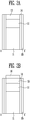
- FIGS. 2A and 2B are cross-sectional views showing light emitting elements according to various embodiments of the present disclosure taken along a line I-I' of FIG. 1
- FIG. 3 is a cross-sectional view schematically showing a polymer film on a surface of an insulating film according to an embodiment of the present disclosure.
- the light emitting element LD according to an embodiment of the present disclosure is shown as a light emitting element having a circular cylinder shape, but a type (e.g., composition) and/or shape of the light emitting element LD according to an embodiment of the present disclosure is not limited thereto.
- the light emitting element LD includes a first semiconductor layer 11, a second semiconductor layer 13, and an active layer 12 interposed between the first and second semiconductor layers 11 and 13.
- the light emitting element LD may include a stacked structure in which the first semiconductor layer 11, the active layer 12, and the second semiconductor layer 13 are sequentially stacked in a length direction.
- the light emitting element LD may be provided in a rod shape extending in one direction.
- the light emitting element LD may have one end and the other end in the length direction.
- one of the first and second semiconductor layers 11 and 13 may be located at one end of the light emitting element LD, and the other of the first and second semiconductor layers 11 and 13 may be located at the other end of the light emitting element LD.
- the light emitting element LD may be a rod-shaped light emitting diode manufactured to have a rod shape.
- the term "rod-shaped” refers to a rod-like shape or bar-like shape that is long (e.g., having an aspect ratio greater than 1) in the length direction, such as a circular cylinder or polygonal cylinder, but a shape of a cross section thereof is not particularly limited.
- the length of the light emitting element LD may be larger than a diameter (or width of the cross section) thereof.
- the light emitting element LD will be described as having a circular cylinder shape, but the present disclosure is not limited thereto.
- the light emitting element LD may have a size that is as small as a nanoscale to a microscale, for example, the light emitting element LD may have a diameter and/or a length of a nanoscale or a microscale range.
- the size of the light emitting element LD in embodiments of the present disclosure is not limited thereto.
- the size of the light emitting element LD may be variously changed according to design conditions of various suitable devices such as, for example a display device, using a light emitting device including the light emitting element LD as a light source.
- the first semiconductor layer 11 may include at least one n-type semiconductor layer.
- the first semiconductor layer 11 may include any one semiconductor material selected from InAlGaN, GaN, AlGaN, InGaN, AlN, and InN, and may include an n-type semiconductor layer doped with a first conductive dopant such as Si, Ge, Sn, and/or the like.
- a first conductive dopant such as Si, Ge, Sn, and/or the like.
- the material constituting the first semiconductor layer 11 is not limited thereto, and the first semiconductor layer 11 may be formed of various suitable materials.
- the active layer 12 may be on the first semiconductor layer 11, and may be formed to have a single or multiple quantum well structure.
- a cladding layer doped with a conductive dopant may be formed on and/or under the active layer 12.
- the cladding layer may be formed of an AlGaN layer and/or an InAlGaN layer.
- materials such as AlGaN and/or AllnGaN may be used to form the active layer 12, and various suitable materials may constitute the active layer 12.
- the light emitting element LD When an electric field of more than a set or predetermined voltage is applied to both ends of the light emitting element LD, the light emitting element LD emits light while electron-hole pairs are coupled in the active layer 12.
- the light emitting element LD By controlling the light emission of the light emitting element LD by using this principle, the light emitting element LD can be used as a light source of various suitable light emitting devices including pixels of the display device.
- the active layer 12 may include one surface contacting the first semiconductor layer 11 and the other surface contacting the second semiconductor layer 13.
- the second semiconductor layer 13 may be on the active layer 12 and may include a semiconductor layer of a different type (e.g., p-type or n-type) from the first semiconductor layer 11.
- the second semiconductor layer 13 may include at least one p-type semiconductor layer.
- the second semiconductor layer 13 may include at least one semiconductor material selected from InAlGaN, GaN, AlGaN, InGaN, AlN, and InN, and may include a p-type semiconductor layer doped with a second conductive dopant such as Mg, and/or the like.
- the material constituting the second semiconductor layer 13 is not limited thereto, and various other suitable materials may constitute the second semiconductor layer 13.
- the light emitting element LD may include an electrode layer 16 on the second semiconductor layer 13.
- the light emitting element LD may include a stacked structure stacked in order of a first semiconductor layer 11, an active layer 12, a second semiconductor layer 13, and an electrode layer 16.
- the stacked structure including the first semiconductor layer 11, the active layer 12, the second semiconductor layer 13, and the electrode layer 16 will be referred to as a light emitting stacked pattern.
- the light emitting stacked pattern may have a circular cylinder shape, and the light emitting element LD may also have a circular cylinder shape corresponding to the light emitting stacked pattern.
- the first semiconductor layer 11, the active layer 12, the second semiconductor layer 13, and the electrode layer 16 included in the light emitting stacked pattern may have a circular cylinder shape.
- the first semiconductor layer 11 may be located at one end of the light emitting element LD, and the electrode layer 16 may be located at the other end of the light emitting element LD.
- the light emitting element LD may include a lower surface of the first semiconductor layer 11 and an upper surface of the electrode layer 16 which are located at both ends of the light emitting element LD and exposed to the external of the light emitting element LD (e.g., exposed to an exterior of the light emitting element LD).
- the lower surface of the first semiconductor layer 11 and the upper surface of the electrode layer 16 may be surfaces electrically coupled by contacting an external conductive material.
- the first semiconductor layer 11 may be under the circular cylinder, and the electrode layer 16 may be on the circular cylinder.
- each of the lower surface of the first semiconductor layer 11 and the upper surface of the electrode layer 16 may be formed in a circular shape (e.g., a substantially circular shape).
- each of the lower surface of the first semiconductor layer 11 and the upper surface of the electrode layer 16 may be formed in an elliptical shape (e.g., a substantially elliptical shape).
- each of the lower surface of the first semiconductor layer 11 and the upper surface of the electrode layer 16 may be formed in a polygonal shape (e.g., a substantially polygonal shape).
- the electrode layer 16 may be an ohmic contact electrode electrically coupled to the second semiconductor layer 13, but is not limited thereto.
- the electrode layer 16 may be a Schottky contact electrode (e.g., an electrode formed by a junction of a semiconductor and a metal).
- the electrode layer 16 may include a metal and/or a metal oxide.
- the electrode layer 16 may include Cr, Ti, Al, Au, Ni, ITO, IZO, ITZO, an oxide, and/or an alloy thereof alone or in combination.
- the electrode layer 16 may be substantially transparent or translucent. Accordingly, light generated in the active layer 12 of the light emitting element LD may be emitted through the electrode layer 16 to the external of the light emitting element LD (e.g., to an exterior of the light emitting element LD).
- the light emitting element LD further includes an insulating film 14 provided on the surface of the light emitting stacked pattern.
- the insulating film 14 may include a transparent insulating material.
- the insulating film 14 may include at least one insulating material selected from the group consisting of SiO 2 , Si 3 N 4 , Al 2 O 3 , and TiO 2 , but is not limited thereto, and may include various other suitable materials having insulation (e.g., that are electrically insulating).
- the insulating film 14 can prevent or reduce electric shorts (e.g., short circuits) that may occur when the active layer 12 contacts a conductive material other than the first semiconductor layer 11 and the second semiconductor layer 13. In addition, the insulating film 14 can minimize or reduce surface defects of the light emitting element LD to improve life-span and efficiency of the light emitting element LD. In addition, when a plurality of light emitting elements LD are located closely to each other, the insulating film 14 can prevent or reduce unwanted electric shorts (e.g., short circuits) that may occur between the light emitting elements LD.
- electric shorts e.g., short circuits
- the insulating film 14 may be formed on the surface of the light emitting stacked pattern to surround at least the outer peripheral (e.g., circumferential) surface of the active layer 12, and may further surround one area of the first and second semiconductor layers 11 and 13 and an outer peripheral (e.g., circumferential) surface of the electrode layer 16.
- the insulating film 14 may expose at least one of both ends of the light emitting element LD having a different polarity.
- the insulating film 14 is shown to surround all outer peripheral (e.g., circumferential) surfaces of first and second semiconductor layers 11 and 13, but the insulating film 14 may be exposed to the outside of the light emitting element LD without covering a portion of the first semiconductor layer 11 of the first and second semiconductor layers 11 and 13 located at both ends of the light emitting element LD in the length direction.
- the insulating film 14 may include an inner surface directly contacting the surface of the light emitting stacked pattern and an outer surface facing the inner surface.
- the insulating film 14 may include an upper surface and a lower surface parallel to (e.g., substantially parallel to) one direction (e.g., horizontal direction) crossing the length direction of the light emitting element.
- the surface of the insulating film 14 may include the outer surface, the upper surface and the lower surface.
- a polymer film 15 is on at least a portion of the surface of the insulating film 14. Providing the polymer film 15 on the surface of the insulating film 14 of the light emitting element LD improves the dispersibility and/or solubility of the light emitting element LD in a composition described herein below. In addition, because the light emitting element LD with the polymer film 15 has excellent dispersion stability in the composition, even after a long time, the light emitting element LD may be homogeneously dispersed in the composition without sinking (e.g., precipitating) in the composition.
- the polymer film 15 is shown to be on the outer surface of the surface of the insulating film 14, but a position of the polymer film 15 is not limited thereto.
- the polymer film 15 may be on the outer surface, the upper surface, and the lower surface of the insulating film 14.
- the polymer film 15 may include a polymer chain PC.
- the polymer chain PC may be provided on the insulating film 14.
- the polymer film 15 may include a linker compound, and the linker compound may couple the surface of the insulating film 14 to an end of the polymer chain PC.
- the polymer chain PC may be introduced to (e.g., bonded to) the surface of the insulating film 14 through the linker compound.
- the linker compound may include a functional group that can be bonded to the surface of the insulating film 14 and the end of the polymer chain PC.
- the linker compound may be a compound containing at least one of a C 1 -C 20 alkylene group, an alkylamine group represented by -(CH 2 ) n -NR 1 - (herein n is an integer of 1 or more ( e.g . 1 to 10), and R 1 is hydrogen or a C 1 -C 20 alkyl group), a C 1 -C 20 ester group, a C 1 -C 20 ketone group, a C 1 -C 20 amide group, and a siloxane group.
- a type (e.g., composition) of the linker compound is not limited thereto, and the linker compound may be selected according to a type (e.g., composition) of a material constituting the insulating film 14 and a type (e.g., composition) of a monomer used for polymerizing the polymer chain PC (e.g., the monomer polymerized to form the polymer chain PC).
- a compound containing a siloxane group may be used as the linker compound.
- any one selected from the following compound 1, compound 2, and compound 3 may be used as a linker compound including the siloxane group.
- the linker compound may be introduced to (e.g., bonded to) the surface of the insulating film 14.
- a methyl group -CH 3 bonded to an oxygen bonded to silicon e.g., an oxygen of a siloxane bond (e.g., Si-O)
- the oxygen atom is bonded to the surface of the insulating film 14.
- a carbon atom to which a halogen atom (e.g., Br and I) is bonded is electrophilic
- the halogen atom may be released from the carbon atom that is electrophilic, and the end of the polymer chain PC is bonded to the released position (e.g., is bonded to the carbon atom that was previously bonded to the halogen atom).
- one end of the linker compound (e.g., compound 1) may be bonded to the surface of the insulating film 14, and the other end of the linker compound may be bonded to the polymer chain PC.
- a method of bonding the polymer chain PC to the linker compound may be a method which uses any suitable polymerization reaction or coupling reaction generally used in the art.
- the polymer chain PC may be grown by bonding a monomer used for polymerization of the polymer chain PC to the end of the linker compound and then performing a polymerization reaction of the monomer at the end of the linker compound (e.g., the polymer chain PC may be grown by polymerizing the monomer from the end of the linker compound).
- the polymer chain PC may be bonded to the linker compound by performing a coupling reaction between the end of the polymer chain PC formed by polymerizing monomers and the end of the linker compound (e.g., the polymer chain PC may be polymerized and then bonded to the linker compound through a coupling reaction).
- a method of bonding the polymer chain PC to the linker compound is not limited thereto.
- the polymer chain PC may include an aliphatic hydrocarbon repeat unit in the main chain.
- the main chain of the polymer chain PC may include a polymerization unit (e.g., repeat unit) derived from an aliphatic hydrocarbon monomer.
- the aliphatic hydrocarbon repeat unit may form a backbone of the polymer chain PC.
- the aliphatic hydrocarbon repeat unit may be included in the polymer chain PC such that there is no aromatic group in the repeat unit of the main chain of the polymer chain PC.
- the aliphatic hydrocarbon repeat unit may include a polar substituent and/or a nonpolar substituent.
- the main chain of the polymer chain PC including the aliphatic hydrocarbon repeat unit may have a carbon number of 10 or more (e.g., all of the aliphatic hydrocarbon repeat units may together include 10 or more carbon atoms).
- the main chain of the polymer chain PC made of the aliphatic hydrocarbon repeat unit may include 10 carbons or more.
- At least one substituent selected from a C 1 -C 20 alkyl group or a C 3 -C 20 alkyl group, a C 2 -C 20 ether group, a C 2 -C 20 ester group, a C 1 -C 20 amine group, a C 2 -C 20 amide group, a hydroxyl group, a C 1 -C 20 alkoxy group, a urethane group, a urea group, an imide group, an acryl group, and a thiol group may be bonded to the main chain of the polymer chain.
- the aliphatic hydrocarbon repeat unit may contain at least one substituent of hydrogen, a C 1 -C 20 alkyl group or a C 3 -C 20 alkyl group, a C 2 -C 20 ether group, a C 2 -C 20 ester group, a C 1 -C 20 amine group, a C 2 -C 20 amide group, a hydroxyl group, a C 1 -C 20 alkoxy group, a urethane group, a urea group, an imide group, an acryl group, or a thiol group.
- a type (e.g., composition) of the substituent included in the aliphatic hydrocarbon repeat unit may be set according to a type (e.g., composition) of the solvent included in the composition.
- the type (e.g., composition) of the solvent included in the composition may be set or determined according to the type (e.g., composition) of the substituent included in the aliphatic hydrocarbon repeat unit. For example, in consideration of the type (e.g., composition) of the substituent included in the main chain of the polymer chain PC and the type (e.g., composition) of the functional group included in the solvent, the light emitting elements with excellent dispersibility and/or solubility in the composition can be implemented.
- the polymer chain PC may include a repeat unit including an aromatic ring in the main chain.
- the main chain of the polymer chain PC may include a polymerization unit derived from a monomer including the aromatic ring.
- the repeat unit including the aromatic ring may form a backbone of a main chain of the polymer chain PC.
- the repeat unit including the aromatic ring may include a polar substituent and/or a nonpolar substituent.
- the main chain of the polymer chain PC including the repeat unit including the aromatic ring may include 10 aromatic rings or more (e.g., all of the repeat units including the aromatic ring may together include 10 or more aromatic rings).
- the main chain of the polymer chain PC including the repeat unit including an aromatic ring may have a carbon number of 10 or more (e.g., may include 10 or more carbon atoms).
- a carbon number of the main chain of the polymer chain PC may refer to the number of carbon atoms included in the main chain except for the carbon included in the aromatic ring.
- the main chain of the polymer chain PC including the repeat unit including an aromatic ring may include 10 or more non-aromatic carbon atoms, where the non-aromatic carbon atoms may be, for example, bridging carbon atoms that couple the repeat units to each other.
- the dispersibility and/or solubility of the light emitting element LD in the solvent may be further improved.
- the repeat unit including the aromatic ring may contain at least one substituent of hydrogen, a C 1 -C 20 alkyl group or a C 3 -C 20 alkyl group, a C 2 -C 20 ether group, a C 2 -C 20 ester group, a C 1 -C 20 amine group, a C 2 -C 20 amide group, a hydroxyl group, a C 1 -C 20 alkoxy group, a urethane group, a urea group, an imide group, an acryl group, or a thiol group.
- a weight average molecular weight of the polymer chain PC may be 2,000 g/mol or more and 1,000,000 g/mol or less (e.g., 2,000 or more daltons to 1,000,000 or less daltons).
- the weight average molecular weight of the polymer chain PC may be 3,000 g/mol (or daltons) or more and 900,000 g/mol (or daltons) or less, 5,000 g/mol (or daltons) or more and 800,000 g/mol (or daltons) or less, 10,000 g/mol (or daltons) or more and 600,000 g/mol (or daltons) or less, 50,000 g/mol (or daltons) or more and 500,000 g/mol (or daltons) or less, or 100,000 g/mol (or daltons) or more and 350,000 g/ mol or less.
- the weight average molecular weight of the polymer chain PC may be 2,000 g/mol (or daltons) or more and 10,000 g/mol (or daltons) or less, 15,000 g/mol (or daltons) or more and 50,000 g/mol (or daltons) or less, 100,000 g/mol (or daltons) or more and 500,000 g/mol (or daltons) or less, or 600,000 g/mol (or daltons) or more and 1,000,000 g/mol (or daltons) or less.
- the weight average molecular weight of the polymer chain PC can be controlled by adjusting the polymerization reaction of the monomer to achieve the desired weight average molecular weight.
- the light emitting element LD having excellent dispersibility and/or solubility in the solvent may be implemented. Therefore, the light emitting element LD may be homogeneously dispersed in the solvent.
- a thickness of the polymer film 15 may be 10 nm or more and 100 nm or less.
- the thickness of the polymer film 15 may be 20 nm or more and 80 nm or less, 30 nm or more and 70 nm or less, or 35 nm or more and 50 nm or less.
- the thickness of the polymer film 15 may be 10 nm or more and 25 nm or less, 30 nm or more and 50 nm or less, or 75 nm or more and 100 nm or less.
- the thickness of the polymer film 15 is within the above-described range, the dispersibility and/or solubility of the light emitting element LD in the solvent may be further improved.
- a defect of the surface of the light emitting element LD may be minimized or reduced to improve the life-span and efficiency of the light emitting element LD.
- the polymer chain PC may include a repeat unit represented by the following Chemical Formula 1.
- each of R 2 and R 2 ' may be independently hydrogen, a C 1 -C 20 alkyl group or a C 3 -C 20 alkyl group, a C 2 -C 20 ether group, a C 2 -C 20 ester group, a C 1 -C 20 amine group, a C 2 -C 20 amide group, a hydroxyl group, a C 1 -C 20 alkoxy group, a urethane group, a urea group, an imide group, an acryl group, or a thiol group.
- each of R 2 and R 2 ' may be independently hydrogen, a C 1 -C 10 alkyl group or a C 3 -C 10 alkyl group, a C 2 -C 10 ether group, a C 2 -C 10 ester group, a hydroxyl group, a C 1 -C 10 alkoxy group, or an acryl group.
- the polymer chain PC may include a repeat unit represented by the following Chemical formula 2.
- each of R 3 and R 3' may be independently hydrogen, a C 1 -C 20 alkyl group or a C 3 -C 20 alkyl group, a C 2 -C 20 ether group, a C 2 -C 20 ester group, a C 1 -C 20 amine group, a C 2 -C 20 amide group, a hydroxyl group, a C 1 -C 20 alkoxy group, a urethane group, a urea group, an imide group, an acryl group, or a thiol group.
- each of R 3 and R 3 ' may be independently hydrogen, a C 1 -C 5 alkyl group or a C 3 -C 5 alkyl group, a C 2 -C 5 ether group, a C 2 -C 5 ester group, a hydroxyl group, a C 1 -C 5 alkoxy group, or an acryl group.
- the polymer chain PC may include a repeat unit represented by the following Chemical Formula 2-1.
- the polymer chain PC may include a repeat unit represented by the following Chemical Formula 3.
- each of R 4 and R 4 ' may be independently hydrogen, a C 1 -C 20 alkyl group or a C 3 -C 20 alkyl group, a C 2 -C 20 ether group, a C 2 -C 20 ester group, a C 1 -C 20 amine group, a C 2 -C 20 amide group, a hydroxyl group, a C 1 -C 20 alkoxy group, a urethane group, a urea group, an imide group, an acryl group, or a thiol group.
- each of R 4 and R 4 ' may be independently a C 1 -C 10 alkyl group, a C 1 -C 10 ether group, a C 1 -C 10 ester group, a hydroxyl group, a C 1 -C 10 alkoxy group, or an acryl group.
- the polymer chain PC may include a repeat unit represented by the following Chemical Formula 3-1.
- the light emitting element LD having the excellent dispersibility and/or solubility in the solvent may be effectively implemented.
- the light emitting element LD described above may be used as a light source of various suitable display devices.
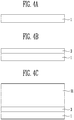
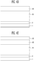
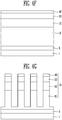
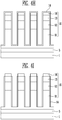
- FIGS. 4A to 4K are cross-sectional views sequentially showing an embodiment of a manufacturing method of a light emitting element.
- a substrate 1, which is configured to support the light emitting element LD, is provided.
- the substrate 1 may be GaAs, GaP, InP, and/or sapphire substrates.
- the substrate 1 may be a wafer for epitaxial growth.
- the substrate 1 may include a ZnO substrate having a GaAs layer on a surface thereof.
- the substrate 1 may include a Ge substrate having a GaAs layer on a surface thereof, and/or a Si substrate having a GaAs layer on a Si wafer with a buffer layer interposed therebetween.
- the substrate 1 may include any suitable commercially available single crystal substrate manufactured by any suitable method generally available in the art. If a selection ratio for manufacturing the light emitting element LD can be satisfied and an epitaxial growth can be smoothly performed, the material of the substrate 1 is not limited thereto. In the following embodiment, the substrate 1 will be described as a sapphire substrate, but the present disclosure is not limited thereto.
- An epitaxial growing surface of the substrate 1 may be smooth.
- the substrate 1 may be changed in size and diameter according to a product to which the substrate 1 is applied, and may be manufactured in a form capable of reducing warpage due to a stacked structure due to the epitaxial growth.
- the shape of the substrate 1 is not limited to a circular shape, but may be, for example, a polygonal shape such as a rectangular shape, and/or the like.
- a sacrificial layer 3 is formed on the substrate 1.
- the sacrificial layer 3 may be formed on the substrate 1 by using a metal organic chemical vapor deposition (MOCVD) method, a molecular beam epitaxy (MBE) method, a vapor-phase epitaxy (VPE) method, a liquid phase epitaxy (LPE) method, and/or the like.
- MOCVD metal organic chemical vapor deposition
- MBE molecular beam epitaxy
- VPE vapor-phase epitaxy
- LPE liquid phase epitaxy
- the substrate 1 and the sacrificial layer 3 may be in contact (e.g., direct or physical contact) with each other.
- the sacrificial layer 3 may be between the light emitting element LD and the substrate 1 in the process of manufacturing the light emitting element LD to physically separate the light emitting element LD and the substrate 1.
- the sacrificial layer 3 may have various suitable shapes of structures, and may have a single layer structure or a multi-layer structure.
- the sacrificial layer 3 may be formed of GaAs, AlAs and/or AlGaAs. Meanwhile, according to the manufacturing method of the light emitting element LD, a step of forming the sacrificial layer 3 on the substrate 1 may be omitted. In this case, the first semiconductor layer 11 may be formed on the substrate 1.
- the first semiconductor layer 11 is formed on the sacrificial layer 3.
- the first semiconductor layer 11 may be formed through the epitaxial growth, and may be formed by using a MOCVD method, an MBE method, a VPE method, an LPE method, or the like.
- an additional semiconductor layer for improving crystallinity such as a buffer layer and a non-doping semiconductor layer, may be further formed between the first semiconductor layer 11 and the sacrificial layer 3.
- the first semiconductor layer 11 may include a semiconductor material composed of group III (e.g., Ga, Al, In) to group V (e.g., P, As), and may include a semiconductor layer doped with a first conductive dopant such as Si, Ge, Sn, and the like.
- group III e.g., Ga, Al, In
- group V e.g., P, As
- the first semiconductor layer 11 may include at least one semiconductor material of GaP, GaAs, GaInP, or AlGaInP doped with Si.
- the first semiconductor layer 11 may include at least one n-type semiconductor layer.
- the material constituting the first semiconductor layer 11 is not limited thereto, and various suitable materials may constitute the first semiconductor layer 11.
- the first active layer 12 is formed on the semiconductor layer 11.
- the active layer 12 may be an area in which electrons and holes recombine, may transition to a lower energy level as the electrons and holes recombine, and may emit light with a corresponding wavelength.
- the active layer 12 may be formed on the first semiconductor layer 11 and may have a single or multiple quantum well structure. A position of the active layer 12 may be changed in various suitable ways according to the type (e.g., composition, shape, etc.) of the light emitting element LD.
- the active layer 12 may include at least one material of GalnP, AlGaInP, GaAs, AlGaAs, InGaAs, InGaAsP, InP, or InAs.
- the active layer 12 can emit light with a wavelength of 400 nm to 900 nm.
- the active layer 12 may use a double heterostructure.
- a cladding layer doped with a conductive dopant may be further formed on the upper surface and / or the lower surface of the active layer 12.
- the second semiconductor layer 13 is formed on the active layer 12.
- the second semiconductor layer 13 may include a semiconductor layer of a type (e.g., p-type or n-type) different from the first semiconductor layer 11.
- the second semiconductor layer 13 may include a semiconductor material composed of group III (e.g., Ga, Al, In) to group V (e.g., P, As), and may include a semiconductor layer doped with a second conductive dopant such as Mg, and the like.
- the second semiconductor layer 13 may include at least one semiconductor material of GaP, GaAs, GaInP, or AlGaInP doped with Mg.
- the second semiconductor layer 13 may include a p-type semiconductor layer.
- the material constituting the second semiconductor layer 13 is not limited thereto, and various suitable materials may constitute the second semiconductor layer 13.
- an electrode layer 16 is formed on the second semiconductor layer 13.
- the electrode layer 16 may include a metal or a metal oxide.
- the electrode layer 16 may include Cr, Ti, Al, Au, Ni, ITO, IZO, ITZO and oxide or alloy thereof alone or in combination.
- the electrode layer 16 may minimize or reduce a loss of light that is generated in the active layer 12 and emitted out of the light emitting element LD, and may be made of a transparent metal oxide such as indium tin oxide (ITO) to improve a current spreading effect to the second semiconductor layer 13.
- ITO indium tin oxide
- the first semiconductor layer 11, the active layer 12, the second semiconductor layer 13 and the electrode layer 16 stacked sequentially on the substrate 1 constitute a light emitting stack.
- the light emitting stack may be etched in a vertical direction to form a light emitting stacked pattern 10.
- a first etching process is performed to pattern the light emitting stack at nanoscale or microscale intervals, thereby forming a plurality of light emitting stacked patterns 10.
- the mask may include a plurality of openings, and one area of the light emitting stack corresponding to the openings is etched to form a groove portion exposing one area of the first semiconductor layer 11 to the outside. Referring to FIG. 4G , one area of the first semiconductor layer 11 facing one surface of the substrate 1 may be exposed to the outside.
- One area of the light emitting stack corresponding to the opening of the mask may be etched, and other area of the light emitting stack not corresponding to the opening of the mask may be not etched. According to the embodiment, the opposite of the above may also be possible. For example, one area of the light emitting stack corresponding to the opening of the mask may not be etched, and one area of the light emitting stack not corresponding to the opening of the mask may be etched.
- a first etching method may be a dry etching method, such as a reactive ion etching (RIE), a reactive ion beam etching (RIBE), or an inductively coupled plasma reactive ion etching (ICP-RIE).
- RIE reactive ion etching
- RIBE reactive ion beam etching
- ICP-RIE inductively coupled plasma reactive ion etching
- each of the light emitting stacked patterns 10 may have a size of nanoscale or microscale.
- residues remaining on the light emitting stacked pattern 10 may be removed through an existing wet etching or dry etching method, but are not limited thereto, and may be removed through an existing removal method.
- the residues may include an etching mask, an insulating material, and the like required for the mask process.
- the insulating film 14 is formed on the light emitting stacked patterns 10 and one area of the first semiconductor layer 11 exposed to the outside.
- the insulating film 14 can cover the first semiconductor layer 11, the active layer 12, the second semiconductor layer 13, and the electrode layer 16 so that the first semiconductor layer 11, the active layer 12, the second semiconductor layer 13, and the electrode layer 16 may be not exposed to the outside.
- the method of forming the insulating film 14 may use a method of applying an insulating material on the light emitting stacked patterns 10 attached on the substrate 1, but is not limited thereto.
- the material that can be used as the insulating film 14 may include at least one insulating material selected from the group consisting of SiO 2 , Si 3 N 4 , Al 2 O 3 , and TiO 2 , but is not limited thereto.
- the Al 2 O 3 film may be formed by atomic layer deposition (ALD), and may be formed by supplying a source made of trimethyl aluminium (TMA) and H 2 O in a pulse form and using chemical adsorption and desorption.
- TMA trimethyl aluminium
- the thickness of the insulating film 14 may be 30 nm to 150 nm, but is not limited thereto.
- a portion of the insulating film 14 can be removed by performing a secondary etching process.
- a portion of the insulating film 14 surrounding the electrode layer 16 and a portion of the insulating film 14 covering one area of the first semiconductor layer 11 facing one surface of the substrate 1 may be removed. Therefore, the insulating film 14 may be provided on the outer surface of the light emitting stacked pattern 10.
- the light emitting stacked pattern 10 surrounded by the insulating film 14 may be formed on the substrate 1 by performing the secondary etching process.
- the light emitting stacked pattern 10 surrounded by the insulating film 14 may be separated from the substrate 1 by using a chemical lift-off (CLO) method.
- the chemical lift-off may be performed at an interface between the first semiconductor layer 11 of the light emitting stacked pattern 10 and the first semiconductor layer 11 formed on the sacrificial layer 3.
- FIG. 4J as the chemical lift-off is performed, a portion of the first semiconductor layer 11 not included in the light emitting stacked pattern 10 is left on the sacrificial layer 3.
- the light emitting stacked pattern 10 separated from the substrate 1 may be a state in which the electrode layer 16, the surface of the insulating film 14, and the lower surface of the first semiconductor layer 11 are exposed to the outside.
- the light emitting element LD may be manufactured by forming the polymer film 15 on the surface of the insulating film 14 of the light emitting stacked pattern 10.
- the polymer film 15 may be formed on at least a portion of the surface of the insulating film 14, and
- FIG. 4K shows an embodiment in which the polymer film 15 is formed on all of the outer surface, upper surface, and lower surface of the insulating film 14.
- the linker compound may be introduced to the surface of the insulating film 14 in a step of forming the polymer film 15.
- the linker compound may be the same as the linker compound described above (e.g. Compounds 1 to 3). As described above, through surface treatment of the insulating film 14, one end of the linker compound may be bonded to the surface of the insulating film 14.
- the step of forming the polymer film 15 may introduce the polymer chain PC to the surface of the insulating film 14 through a linker compound.
- the end of the polymer chain PC may be bonded to the other end of the linker compound.
- the linker compound may couple the polymer chain PC to the surface of the insulating film 14.
- the method of bonding the polymer chain PC to the linker compound may be a method which uses a polymerization reaction or a coupling reaction used in the prior art.
- the polymer chain PC may be grown by bonding a monomer used for polymerization of the polymer chain PC to the end of the linker compound and then performing a polymerization reaction of the monomer at the end of the linker compound.
- the polymer chain PC may be bonded to the linker compound by performing a coupling reaction between the end of the polymer chain PC formed by polymerizing monomers and the end of the linker compound.
- a method of bonding the polymer chain PC to the linker compound is not limit thereto.
- FIG. 5 is a drawing showing a composition including a light emitting element according to an embodiment of the present disclosure.
- a composition C may include a solvent S and a light emitting element LD.
- the composition C may be an ink composition used to provide a light emitting element LD in a process of manufacturing a display device.
- the solvent S may contain at least one of an alkyl solvent containing an alkyl group (e.g., an alkyl solvent containing a compound including an alkyl group), an ether solvent containing an ether group (e.g., an ether solvent containing a compound including an ether group), an ester solvent containing an ester group (e.g., an ester solvent containing a compound including an ester group), an amine solvent containing an amine group (e.g., an amine solvent containing a compound including an amine group), an amide solvent containing an amide group (e.g., an amide solvent containing a compound including an amide group), an alcohol solvent containing an alcohol group (e.g., an alcohol solvent containing a compound including an alcohol group), a urethane solvent containing a urethane group (e.g., a urethane solvent containing a compound including a urethane group), a urea solvent containing an alkyl group
- a type (e.g., composition) of the solvent S included in the composition C a type (e.g., composition) of the repeat unit constituting the main chain of the polymer chain PC and a type (e.g., composition) of a substituent included in the repeat unit may be set.
- the type (e.g., composition) of solvent S included in the composition C may be set or determined according to the type (e.g., composition) of the repeat unit constituting the main chain of the polymer chain PC and the type (e.g., composition) of the substituent included in the repeat unit.
- the composition C including the light emitting element LD having excellent dispersibility and/or solubility in the solvent S may be implemented.
- the light emitting element LD can be homogeneously dispersed in the composition C, and the light emitting element LD may not precipitate or aggregate in the solvent, even after a long time.
- the composition C it is possible to provide a set or predetermined number of light emitting elements LD per pixel of the display device.
- the polymer chain PC may be provided in a form of an organic and/or an inorganic salt. Because the polymer chain PC is provided in the solvent S in the form of an organic and/or an inorganic salt, the dispersibility and/or solubility of the light emitting element LD can be further improved.
Landscapes
- Chemical & Material Sciences (AREA)
- Organic Chemistry (AREA)
- Chemical Kinetics & Catalysis (AREA)
- Polymers & Plastics (AREA)
- Medicinal Chemistry (AREA)
- Health & Medical Sciences (AREA)
- Materials Engineering (AREA)
- Wood Science & Technology (AREA)
- Engineering & Computer Science (AREA)
- Life Sciences & Earth Sciences (AREA)
- Addition Polymer Or Copolymer, Post-Treatments, Or Chemical Modifications (AREA)
- Led Device Packages (AREA)
- Electroluminescent Light Sources (AREA)
- Semiconductor Lasers (AREA)
- Led Devices (AREA)
- Compositions Of Macromolecular Compounds (AREA)
Abstract
Description
- Embodiments of the present disclosure relate to a light emitting element, a method of manufacturing of the light emitting element, and a composition including the light emitting element.
- A light emitting diode (hereinafter referred to as LED) has relatively good durability even in harsh environmental conditions and has excellent performance in terms of life-span and luminance. Recently, researches for applying such LEDs to various display devices have been actively conducted.
- As a part of this research, a technique for manufacturing an ultra-small rod-shaped LED, which is as small as a micro scale or a nano scale, has been developed using an inorganic crystal structure, for example, a structure in which a nitride semiconductor is grown. For example, the rod-shaped LED may be manufactured in a size small enough to constitute a pixel of a self-luminous display device.
- An embodiment of the present disclosure provides a light emitting element having excellent dispersibility and dispersion stability in a solution, a method of manufacturing the light emitting element, and a composition including the light emitting element.
- A light emitting element according to an embodiment of the present disclosure includes a first semiconductor layer; an active layer on the first semiconductor layer; a second semiconductor layer on the active layer; an insulating film surrounding an outer peripheral surface of each of the first semiconductor layer, the active layer and the second semiconductor layer; and a polymer film including a polymer chain and on at least a portion of a surface of the insulating film.
- In an embodiment of the present disclosure, the light emitting element may further include an electrode layer on the second semiconductor layer.
- In an embodiment of the present disclosure, the polymer film may further include a linker compound coupling the surface of the insulating film and an end of the polymer chain.
- In an embodiment of the present disclosure, the linker compound may be a compound containing at least one of a C1-C20 alkylene group, an alkylamine group represented by -(CH2)n-NR1- (wherein n is an integer of 1 or more, and R1 is hydrogen or a C1-C20 alkyl group), a C1-C20 ester group, a C1-C20 ketone group, a C1-C20 amide group, and a siloxane group.
- In an embodiment of the present disclosure, the polymer chain may include an aliphatic hydrocarbon repeat unit in a main chain.
- In an embodiment of the present disclosure, the main chain of the polymer chain may have a carbon number of 10 or more.
- In an embodiment of the present disclosure, the polymer chain may include a repeat unit including an aromatic ring in the main chain.
- In an embodiment of the present disclosure, a main chain of the polymer chain may include 10 or more aromatic rings.
- In an embodiment of the present disclosure, at least one substituent selected from a C1-C20 alkyl group or a C3-C20 alkyl group, a C2-C20 ether group, a C2-C20 ester group, a C1-C20 amine group, a C2-C20 amide group, a hydroxyl group, a C1-C20 alkoxy group, a urethane group, a urea group, an imide group, an acryl group and a thiol group may be bonded to the main chain of the polymer chain.
- In an embodiment of the present disclosure, the polymer chain may include a repeat unit represented by a following Chemical Formula 1.

- In
Chemical Formula 1, each of R2 and R2' is independently hydrogen, a C1-C20 alkyl group or a C3-C20 alkyl group, a C2-C20 ether group, a C2-C20 ester group, a C1-C20 amine group, a C2-C20 amide group, a hydroxyl group, a C1-C20 alkoxy group, a urethane group, a urea group, an imide group, an acryl group, or a thiol group. - In an embodiment of the present disclosure, the polymer chain may include a repeat unit represented by a following Chemical Formula 2.

- In Chemical Formula 2, each of R3 and R3' is independently hydrogen, a C1-C20 alkyl group or a C3-C20 alkyl group, a C2-C20 ether group, a C2-C20 ester group, a C1-C20 amine group, a C2-C20 amide group, a hydroxyl group, a C1-C20 alkoxy group, a urethane group, a urea group, an imide group, an acryl group, or a thiol group.
- In an embodiment of the present disclosure, the polymer chain may include a repeat unit represented by a following Chemical Formula 3.


- In
Chemical Formula 3, each of R4 and R4' is independently hydrogen, a C1-C20 alkyl group or a C3-C20 alkyl group, a C2-C20 ether group, a C2-C20 ester group, a C1-C20 amine group, a C2-C20 amide group, a hydroxyl group, a C1-C20 alkoxy group, a urethane group, a urea group, an imide group, an acryl group, or a thiol group. - In an embodiment of the present disclosure, a weight average molecular weight of the polymer chain may be 2,000 g/mol or more and 1,000,000 g/mol or less.
- In an embodiment of the present disclosure, a thickness of the polymer film may be 10 nm or more and 100 nm or less.
- A method of manufacturing a light emitting element according to an embodiment of the present disclosure includes forming a light emitting stack in which a first semiconductor layer, an active layer, and a second semiconductor layer are sequentially stacked on a substrate; etching the light emitting stack to form a light emitting stacked pattern; forming an insulating film on the light emitting stacked pattern; and forming a polymer film including a polymer chain on at least portion of a surface of the insulating film.
- In an embodiment of the present disclosure, the forming the polymer film may include introducing a linker compound to a surface of the insulating film.
- In an embodiment of the present disclosure, in the forming the polymer film, an end of the polymer chain formed by polymerization of monomers may be bonded to the linker compound.
- In an embodiment of the present disclosure, in the forming the polymer film, monomers may be polymerized in the linker compound to form the polymer chain.
- A composition according to an embodiment of the present disclosure includes a solvent; and a light emitting element. The light emitting element includes a first semiconductor layer; an active layer on the first semiconductor layer; a second semiconductor layer on the active layer; an insulating film surrounding an outer peripheral surface of each of the first semiconductor layer, the active layer and the second semiconductor layer; and a polymer film including a polymer chain and on at least a portion of a surface of the insulating film.
- In an embodiment of the present disclosure, the solvent contains at least one of an alkyl solvent containing an alkyl group, an ether solvent containing an ether group, an ester solvent containing an ester group, an amine solvent containing an amine group, an amide solvent containing an amide group, an alcohol solvent containing an alcohol group, a urethane solvent containing a urethane group, a urea solvent containing a urea group, an imide solvent containing an imide group, an acrylic solvent containing an acrylic group, or a thiol solvent containing a thiol group.
- An embodiment of the present disclosure can provide light a light emitting element having excellent dispersibility and/or solubility in a solvent.
- For example, according to an embodiment of the present disclosure, by providing a polymer film containing a polymer chain to the light emitting element, it is possible to improve the dispersibility and dispersion stability in the solvent.
- At least some of the above and other features of the invention are set out in the claims.
- However, the effect of the present disclosure is not limited to the effects described above, but may be variously extended in a range that does not depart from the scope of the present disclosure.
- The accompanying drawings, together with the specification, illustrate embodiments of the subject matter of the present disclosure, and, together with the description, serve to explain principles of embodiments of the subject matter of the present disclosure.
-
FIG. 1 is a perspective view showing a light emitting element according to an embodiment of the present disclosure. -
FIGS. 2A and 2B are cross-sectional views showing light emitting elements according to various embodiments of the present disclosure taken along a line I-I' ofFIG. 1 . -
FIG. 3 is a cross-sectional view schematically showing a polymer film on a surface of an insulating film according to an embodiment of the present disclosure. -
FIGS. 4A to 4K are cross-sectional views sequentially showing a manufacturing method of a light emitting element. -
FIG. 5 is a drawing showing a composition including a light emitting element according to an embodiment of the present disclosure. - It will be apparent to those skilled in the art that various modifications and variations can be made to the subject matter of the present disclosure without departing from the scope of the disclosure, and certain embodiments are exemplified in the drawings and explained in the detailed description. Thus, it is intended that the present disclosure covers suitable modifications and variations of the subject matter of this disclosure provided they come within the scope of the present disclosure and their equivalents.
- Like reference numerals designate like elements throughout the specification. In the accompanying drawings, dimensions of structures may be exaggerated for clarity. The terms, 'first', 'second' and the like may be simply used for description of various constituent elements, but those meanings may not be limited to the restricted meanings. The above terms are used only for distinguishing one constituent element from other constituent elements. For example, a first constituent element may be referred to as a second constituent element and similarly, the second constituent element may be referred to as the first constituent element within the scope of the appended claims. When explaining the singular, unless explicitly described to the contrary, it may be interpreted as the plural meaning.
- In the specification, the word "comprise" or "has" is used to specify existence of a feature, a number, a process, an operation, a constituent element, a part, or a combination thereof, and it will be understood that existence or additional possibility of one or more other features or numbers, processes, operations, constituent elements, parts, or combinations thereof are not excluded in advance. In addition, it will be understood that when an element such as a layer, film, region, or substrate is referred to as being "on" another element, it can be directly on the other element or intervening elements may also be present. In the specification, it will be understood that when an element such as a layer, film, region, or substrate is referred to as being "on" another element, the direction of the stacking is not limited to an upper direction and may include stacking in a side direction or a lower direction. Additionally, it will be understood that when an element such as a layer, film, region, or substrate is referred to as being "beneath" another element, it can be directly beneath the other element or intervening elements may also be present.
- In the present specification, the term "repeat unit" may refer to a form in which a monomer is reacted in a polymer, and may refer to a form in which monomers form a backbone of the polymer e.g., a main chain of the polymer chain through a polymerization reaction.
- Hereinafter, embodiments of the present disclosure will be described in further detail with reference to the accompanying drawings.
-
FIG. 1 is a perspective view showing a light emitting element according to an embodiment of the present disclosure,FIGS. 2A and 2B are cross-sectional views showing light emitting elements according to various embodiments of the present disclosure taken along a line I-I' ofFIG. 1 , andFIG. 3 is a cross-sectional view schematically showing a polymer film on a surface of an insulating film according to an embodiment of the present disclosure. - In
FIG. 1 , the light emitting element LD according to an embodiment of the present disclosure is shown as a light emitting element having a circular cylinder shape, but a type (e.g., composition) and/or shape of the light emitting element LD according to an embodiment of the present disclosure is not limited thereto. - Referring to
FIGS. 1 to 2B , the light emitting element LD according to an embodiment of the present disclosure includes afirst semiconductor layer 11, asecond semiconductor layer 13, and anactive layer 12 interposed between the first and second semiconductor layers 11 and 13. According to an embodiment, the light emitting element LD may include a stacked structure in which thefirst semiconductor layer 11, theactive layer 12, and thesecond semiconductor layer 13 are sequentially stacked in a length direction. - The light emitting element LD may be provided in a rod shape extending in one direction. When an extending direction of the light emitting element LD is referred to as a length direction, the light emitting element LD may have one end and the other end in the length direction. According to an embodiment, one of the first and second semiconductor layers 11 and 13 may be located at one end of the light emitting element LD, and the other of the first and second semiconductor layers 11 and 13 may be located at the other end of the light emitting element LD.
- The light emitting element LD may be a rod-shaped light emitting diode manufactured to have a rod shape. In this specification, the term "rod-shaped" refers to a rod-like shape or bar-like shape that is long (e.g., having an aspect ratio greater than 1) in the length direction, such as a circular cylinder or polygonal cylinder, but a shape of a cross section thereof is not particularly limited. For example, the length of the light emitting element LD may be larger than a diameter (or width of the cross section) thereof. Hereinafter, for better understanding and ease of description, the light emitting element LD will be described as having a circular cylinder shape, but the present disclosure is not limited thereto.
- According to an embodiment, the light emitting element LD may have a size that is as small as a nanoscale to a microscale, for example, the light emitting element LD may have a diameter and/or a length of a nanoscale or a microscale range. However, the size of the light emitting element LD in embodiments of the present disclosure is not limited thereto. For example, the size of the light emitting element LD may be variously changed according to design conditions of various suitable devices such as, for example a display device, using a light emitting device including the light emitting element LD as a light source.
- For example, the
first semiconductor layer 11 may include at least one n-type semiconductor layer. For example, thefirst semiconductor layer 11 may include any one semiconductor material selected from InAlGaN, GaN, AlGaN, InGaN, AlN, and InN, and may include an n-type semiconductor layer doped with a first conductive dopant such as Si, Ge, Sn, and/or the like. However, the material constituting thefirst semiconductor layer 11 is not limited thereto, and thefirst semiconductor layer 11 may be formed of various suitable materials. - The
active layer 12 may be on thefirst semiconductor layer 11, and may be formed to have a single or multiple quantum well structure. In an embodiment, a cladding layer doped with a conductive dopant may be formed on and/or under theactive layer 12. For example, the cladding layer may be formed of an AlGaN layer and/or an InAlGaN layer. According to an embodiment, materials such as AlGaN and/or AllnGaN may be used to form theactive layer 12, and various suitable materials may constitute theactive layer 12. - When an electric field of more than a set or predetermined voltage is applied to both ends of the light emitting element LD, the light emitting element LD emits light while electron-hole pairs are coupled in the
active layer 12. By controlling the light emission of the light emitting element LD by using this principle, the light emitting element LD can be used as a light source of various suitable light emitting devices including pixels of the display device. Theactive layer 12 may include one surface contacting thefirst semiconductor layer 11 and the other surface contacting thesecond semiconductor layer 13. - The
second semiconductor layer 13 may be on theactive layer 12 and may include a semiconductor layer of a different type (e.g., p-type or n-type) from thefirst semiconductor layer 11. For example, thesecond semiconductor layer 13 may include at least one p-type semiconductor layer. For example, thesecond semiconductor layer 13 may include at least one semiconductor material selected from InAlGaN, GaN, AlGaN, InGaN, AlN, and InN, and may include a p-type semiconductor layer doped with a second conductive dopant such as Mg, and/or the like. However, the material constituting thesecond semiconductor layer 13 is not limited thereto, and various other suitable materials may constitute thesecond semiconductor layer 13. - Referring to
FIG. 2B , in an embodiment of the present disclosure, the light emitting element LD may include anelectrode layer 16 on thesecond semiconductor layer 13. For example, the light emitting element LD may include a stacked structure stacked in order of afirst semiconductor layer 11, anactive layer 12, asecond semiconductor layer 13, and anelectrode layer 16. In the embodiment described below, the stacked structure including thefirst semiconductor layer 11, theactive layer 12, thesecond semiconductor layer 13, and theelectrode layer 16 will be referred to as a light emitting stacked pattern. - The light emitting stacked pattern may have a circular cylinder shape, and the light emitting element LD may also have a circular cylinder shape corresponding to the light emitting stacked pattern. In addition, the
first semiconductor layer 11, theactive layer 12, thesecond semiconductor layer 13, and theelectrode layer 16 included in the light emitting stacked pattern may have a circular cylinder shape. - The
first semiconductor layer 11 may be located at one end of the light emitting element LD, and theelectrode layer 16 may be located at the other end of the light emitting element LD. The light emitting element LD may include a lower surface of thefirst semiconductor layer 11 and an upper surface of theelectrode layer 16 which are located at both ends of the light emitting element LD and exposed to the external of the light emitting element LD (e.g., exposed to an exterior of the light emitting element LD). The lower surface of thefirst semiconductor layer 11 and the upper surface of theelectrode layer 16 may be surfaces electrically coupled by contacting an external conductive material. - When the light emitting element LD has a circular cylinder shape, the
first semiconductor layer 11 may be under the circular cylinder, and theelectrode layer 16 may be on the circular cylinder. When the light emitting element LD has a circular cylinder shape, each of the lower surface of thefirst semiconductor layer 11 and the upper surface of theelectrode layer 16 may be formed in a circular shape (e.g., a substantially circular shape). - According to the embodiment, when the light emitting element LD has an elliptical cylinder shape, each of the lower surface of the
first semiconductor layer 11 and the upper surface of theelectrode layer 16 may be formed in an elliptical shape (e.g., a substantially elliptical shape). In addition, according to another embodiment, when the light emitting element LD has a polygonal cylinder shape, each of the lower surface of thefirst semiconductor layer 11 and the upper surface of theelectrode layer 16 may be formed in a polygonal shape (e.g., a substantially polygonal shape). - The
electrode layer 16 may be an ohmic contact electrode electrically coupled to thesecond semiconductor layer 13, but is not limited thereto. According to an embodiment, theelectrode layer 16 may be a Schottky contact electrode (e.g., an electrode formed by a junction of a semiconductor and a metal). Theelectrode layer 16 may include a metal and/or a metal oxide. For example, theelectrode layer 16 may include Cr, Ti, Al, Au, Ni, ITO, IZO, ITZO, an oxide, and/or an alloy thereof alone or in combination. In addition, theelectrode layer 16 may be substantially transparent or translucent. Accordingly, light generated in theactive layer 12 of the light emitting element LD may be emitted through theelectrode layer 16 to the external of the light emitting element LD (e.g., to an exterior of the light emitting element LD). - As shown in
FIGS. 1 to 2B , the light emitting element LD further includes an insulatingfilm 14 provided on the surface of the light emitting stacked pattern. The insulatingfilm 14 may include a transparent insulating material. For example, the insulatingfilm 14 may include at least one insulating material selected from the group consisting of SiO2, Si3N4, Al2O3, and TiO2, but is not limited thereto, and may include various other suitable materials having insulation (e.g., that are electrically insulating). - The insulating
film 14 can prevent or reduce electric shorts (e.g., short circuits) that may occur when theactive layer 12 contacts a conductive material other than thefirst semiconductor layer 11 and thesecond semiconductor layer 13. In addition, the insulatingfilm 14 can minimize or reduce surface defects of the light emitting element LD to improve life-span and efficiency of the light emitting element LD. In addition, when a plurality of light emitting elements LD are located closely to each other, the insulatingfilm 14 can prevent or reduce unwanted electric shorts (e.g., short circuits) that may occur between the light emitting elements LD. - The insulating
film 14 may be formed on the surface of the light emitting stacked pattern to surround at least the outer peripheral (e.g., circumferential) surface of theactive layer 12, and may further surround one area of the first and second semiconductor layers 11 and 13 and an outer peripheral (e.g., circumferential) surface of theelectrode layer 16. - In an embodiment of the present disclosure, the insulating
film 14 may expose at least one of both ends of the light emitting element LD having a different polarity. InFIGS. 1 to 2B , the insulatingfilm 14 is shown to surround all outer peripheral (e.g., circumferential) surfaces of first and second semiconductor layers 11 and 13, but the insulatingfilm 14 may be exposed to the outside of the light emitting element LD without covering a portion of thefirst semiconductor layer 11 of the first and second semiconductor layers 11 and 13 located at both ends of the light emitting element LD in the length direction. - The insulating
film 14 may include an inner surface directly contacting the surface of the light emitting stacked pattern and an outer surface facing the inner surface. In addition, the insulatingfilm 14 may include an upper surface and a lower surface parallel to (e.g., substantially parallel to) one direction (e.g., horizontal direction) crossing the length direction of the light emitting element. In some embodiments, the surface of the insulatingfilm 14 may include the outer surface, the upper surface and the lower surface. - Referring to
FIGS. 1 to 2B , in an embodiment of the present disclosure, apolymer film 15 is on at least a portion of the surface of the insulatingfilm 14. Providing thepolymer film 15 on the surface of the insulatingfilm 14 of the light emitting element LD improves the dispersibility and/or solubility of the light emitting element LD in a composition described herein below. In addition, because the light emitting element LD with thepolymer film 15 has excellent dispersion stability in the composition, even after a long time, the light emitting element LD may be homogeneously dispersed in the composition without sinking (e.g., precipitating) in the composition. - In
FIGS. 1 to 2B , thepolymer film 15 is shown to be on the outer surface of the surface of the insulatingfilm 14, but a position of thepolymer film 15 is not limited thereto. For example, thepolymer film 15 may be on the outer surface, the upper surface, and the lower surface of the insulatingfilm 14. - In an embodiment of the present disclosure, as shown in
FIG. 3 , thepolymer film 15 may include a polymer chain PC. In this case, the polymer chain PC may be provided on the insulatingfilm 14. For example, thepolymer film 15 may include a linker compound, and the linker compound may couple the surface of the insulatingfilm 14 to an end of the polymer chain PC. In some embodiments, the polymer chain PC may be introduced to (e.g., bonded to) the surface of the insulatingfilm 14 through the linker compound. - The linker compound may include a functional group that can be bonded to the surface of the insulating
film 14 and the end of the polymer chain PC. For example, the linker compound may be a compound containing at least one of a C1-C20 alkylene group, an alkylamine group represented by -(CH2)n-NR1- (herein n is an integer of 1 or more (e.g. 1 to 10), and R1 is hydrogen or a C1-C20 alkyl group), a C1-C20 ester group, a C1-C20 ketone group, a C1-C20 amide group, and a siloxane group. However, a type (e.g., composition) of the linker compound is not limited thereto, and the linker compound may be selected according to a type (e.g., composition) of a material constituting the insulatingfilm 14 and a type (e.g., composition) of a monomer used for polymerizing the polymer chain PC (e.g., the monomer polymerized to form the polymer chain PC). - In an embodiment of the present disclosure, a compound containing a siloxane group may be used as the linker compound. For example, any one selected from the following
compound 1, compound 2, andcompound 3 may be used as a linker compound including the siloxane group.


- Hereinafter, embodiments of the present disclosure will be described according to an embodiment using a compound containing the siloxane group as a linker compound.
- Through a surface treatment of the insulating
film 14, the linker compound may be introduced to (e.g., bonded to) the surface of the insulatingfilm 14. For example, through the surface treatment of the insulatingfilm 14, in thecompound 1 tocompound 3, a methyl group -CH3 bonded to an oxygen bonded to silicon (e.g., an oxygen of a siloxane bond (e.g., Si-O)) of the siloxane group may be released, and the oxygen atom is bonded to the surface of the insulatingfilm 14. In thecompound 1 tocompound 3, a carbon atom to which a halogen atom (e.g., Br and I) is bonded is electrophilic, the halogen atom may be released from the carbon atom that is electrophilic, and the end of the polymer chain PC is bonded to the released position (e.g., is bonded to the carbon atom that was previously bonded to the halogen atom). - Therefore, as shown in
FIG. 3 , one end of the linker compound (e.g., compound 1) may be bonded to the surface of the insulatingfilm 14, and the other end of the linker compound may be bonded to the polymer chain PC. - A method of bonding the polymer chain PC to the linker compound may be a method which uses any suitable polymerization reaction or coupling reaction generally used in the art. For example, the polymer chain PC may be grown by bonding a monomer used for polymerization of the polymer chain PC to the end of the linker compound and then performing a polymerization reaction of the monomer at the end of the linker compound (e.g., the polymer chain PC may be grown by polymerizing the monomer from the end of the linker compound). In addition, the polymer chain PC may be bonded to the linker compound by performing a coupling reaction between the end of the polymer chain PC formed by polymerizing monomers and the end of the linker compound (e.g., the polymer chain PC may be polymerized and then bonded to the linker compound through a coupling reaction). However, a method of bonding the polymer chain PC to the linker compound is not limited thereto.
- In an embodiment of the present disclosure, the polymer chain PC may include an aliphatic hydrocarbon repeat unit in the main chain. For example, the main chain of the polymer chain PC may include a polymerization unit (e.g., repeat unit) derived from an aliphatic hydrocarbon monomer. The aliphatic hydrocarbon repeat unit may form a backbone of the polymer chain PC. In the present disclosure, the aliphatic hydrocarbon repeat unit may be included in the polymer chain PC such that there is no aromatic group in the repeat unit of the main chain of the polymer chain PC. In addition, the aliphatic hydrocarbon repeat unit may include a polar substituent and/or a nonpolar substituent.
- The main chain of the polymer chain PC including the aliphatic hydrocarbon repeat unit may have a carbon number of 10 or more (e.g., all of the aliphatic hydrocarbon repeat units may together include 10 or more carbon atoms). For example, the main chain of the polymer chain PC made of the aliphatic hydrocarbon repeat unit may include 10 carbons or more. By providing the polymer chain PC including the main chain having a carbon number of 10 or more to the surface of the insulating
film 14 of the light emitting element LD, solubility and/or dispersibility of the light emitting element LD in a solvent may be increased. - In an embodiment of the present disclosure, at least one substituent selected from a C1-C20 alkyl group or a C3-C20 alkyl group, a C2-C20 ether group, a C2-C20 ester group, a C1-C20 amine group, a C2-C20 amide group, a hydroxyl group, a C1-C20 alkoxy group, a urethane group, a urea group, an imide group, an acryl group, and a thiol group may be bonded to the main chain of the polymer chain.
- In some embodiments, the aliphatic hydrocarbon repeat unit may contain at least one substituent of hydrogen, a C1-C20 alkyl group or a C3-C20 alkyl group, a C2-C20 ether group, a C2-C20 ester group, a C1-C20 amine group, a C2-C20 amide group, a hydroxyl group, a C1-C20 alkoxy group, a urethane group, a urea group, an imide group, an acryl group, or a thiol group.
- As described herein below, a type (e.g., composition) of the substituent included in the aliphatic hydrocarbon repeat unit may be set according to a type (e.g., composition) of the solvent included in the composition. In some embodiments, the type (e.g., composition) of the solvent included in the composition may be set or determined according to the type (e.g., composition) of the substituent included in the aliphatic hydrocarbon repeat unit. For example, in consideration of the type (e.g., composition) of the substituent included in the main chain of the polymer chain PC and the type (e.g., composition) of the functional group included in the solvent, the light emitting elements with excellent dispersibility and/or solubility in the composition can be implemented.
- In an embodiment of the present disclosure, the polymer chain PC may include a repeat unit including an aromatic ring in the main chain. For example, the main chain of the polymer chain PC may include a polymerization unit derived from a monomer including the aromatic ring. The repeat unit including the aromatic ring may form a backbone of a main chain of the polymer chain PC. In addition, the repeat unit including the aromatic ring may include a polar substituent and/or a nonpolar substituent.
- The main chain of the polymer chain PC including the repeat unit including the aromatic ring may include 10 aromatic rings or more (e.g., all of the repeat units including the aromatic ring may together include 10 or more aromatic rings). In addition, the main chain of the polymer chain PC including the repeat unit including an aromatic ring may have a carbon number of 10 or more (e.g., may include 10 or more carbon atoms). In this case, a carbon number of the main chain of the polymer chain PC may refer to the number of carbon atoms included in the main chain except for the carbon included in the aromatic ring. For example, the main chain of the polymer chain PC including the repeat unit including an aromatic ring may include 10 or more non-aromatic carbon atoms, where the non-aromatic carbon atoms may be, for example, bridging carbon atoms that couple the repeat units to each other.
- By providing the polymer chain PC including the main chain having an aromatic ring of a number of 10 or more (e.g., including 10 or more aromatic rings) and a carbon number of 10 or more (e.g., including 10 or more non-aromatic carbon atoms) on the surface of the insulating
film 14 of the light emitting element LD, the dispersibility and/or solubility of the light emitting element LD in the solvent may be further improved. - In an embodiment of the present disclosure, the repeat unit including the aromatic ring may contain at least one substituent of hydrogen, a C1-C20 alkyl group or a C3-C20 alkyl group, a C2-C20 ether group, a C2-C20 ester group, a C1-C20 amine group, a C2-C20 amide group, a hydroxyl group, a C1-C20 alkoxy group, a urethane group, a urea group, an imide group, an acryl group, or a thiol group.
- In an embodiment of the present disclosure, a weight average molecular weight of the polymer chain PC may be 2,000 g/mol or more and 1,000,000 g/mol or less (e.g., 2,000 or more daltons to 1,000,000 or less daltons). For example, the weight average molecular weight of the polymer chain PC may be 3,000 g/mol (or daltons) or more and 900,000 g/mol (or daltons) or less, 5,000 g/mol (or daltons) or more and 800,000 g/mol (or daltons) or less, 10,000 g/mol (or daltons) or more and 600,000 g/mol (or daltons) or less, 50,000 g/mol (or daltons) or more and 500,000 g/mol (or daltons) or less, or 100,000 g/mol (or daltons) or more and 350,000 g/ mol or less.
- For example, the weight average molecular weight of the polymer chain PC may be 2,000 g/mol (or daltons) or more and 10,000 g/mol (or daltons) or less, 15,000 g/mol (or daltons) or more and 50,000 g/mol (or daltons) or less, 100,000 g/mol (or daltons) or more and 500,000 g/mol (or daltons) or less, or 600,000 g/mol (or daltons) or more and 1,000,000 g/mol (or daltons) or less. The weight average molecular weight of the polymer chain PC can be controlled by adjusting the polymerization reaction of the monomer to achieve the desired weight average molecular weight.
- By adjusting the weight average molecular weight of the polymer chain PC in the above-described range, the light emitting element LD having excellent dispersibility and/or solubility in the solvent may be implemented. Therefore, the light emitting element LD may be homogeneously dispersed in the solvent.
- In an embodiment of the present disclosure, a thickness of the
polymer film 15 may be 10 nm or more and 100 nm or less. For example, the thickness of thepolymer film 15 may be 20 nm or more and 80 nm or less, 30 nm or more and 70 nm or less, or 35 nm or more and 50 nm or less. In some embodiments, the thickness of thepolymer film 15 may be 10 nm or more and 25 nm or less, 30 nm or more and 50 nm or less, or 75 nm or more and 100 nm or less. - When the thickness of the
polymer film 15 is within the above-described range, the dispersibility and/or solubility of the light emitting element LD in the solvent may be further improved. In addition, by adjusting the thickness of thepolymer film 15 in the above-described range, a defect of the surface of the light emitting element LD may be minimized or reduced to improve the life-span and efficiency of the light emitting element LD. - In an embodiment of the present disclosure, the polymer chain PC may include a repeat unit represented by the following
Chemical Formula 1.
- In
Chemical Formula 1, each of R2 and R2' may be independently hydrogen, a C1-C20 alkyl group or a C3-C20 alkyl group, a C2-C20 ether group, a C2-C20 ester group, a C1-C20 amine group, a C2-C20 amide group, a hydroxyl group, a C1-C20 alkoxy group, a urethane group, a urea group, an imide group, an acryl group, or a thiol group. - In some embodiments, in
Chemical Formula 1, each of R2 and R2' may be independently hydrogen, a C1-C10 alkyl group or a C3-C10 alkyl group, a C2-C10 ether group, a C2-C10 ester group, a hydroxyl group, a C1-C10 alkoxy group, or an acryl group. - In an embodiment of the present disclosure, the polymer chain PC may include a repeat unit represented by the following Chemical formula 2.

- In Chemical Formula 2, each of R3 and R3' may be independently hydrogen, a C1-C20 alkyl group or a C3-C20 alkyl group, a C2-C20 ether group, a C2-C20 ester group, a C1-C20 amine group, a C2-C20 amide group, a hydroxyl group, a C1-C20 alkoxy group, a urethane group, a urea group, an imide group, an acryl group, or a thiol group.
- In some embodiments, in Chemical Formula 2, each of R3 and R3' may be independently hydrogen, a C1-C5 alkyl group or a C3-C5 alkyl group, a C2-C5 ether group, a C2-C5 ester group, a hydroxyl group, a C1-C5 alkoxy group, or an acryl group.
- In an embodiment of the present disclosure, the polymer chain PC may include a repeat unit represented by the following Chemical Formula 2-1.

- In an embodiment of the present disclosure, the polymer chain PC may include a repeat unit represented by the following
Chemical Formula 3.
- In
Chemical Formula 3, each of R4 and R4' may be independently hydrogen, a C1-C20 alkyl group or a C3-C20 alkyl group, a C2-C20 ether group, a C2-C20 ester group, a C1-C20 amine group, a C2-C20 amide group, a hydroxyl group, a C1-C20 alkoxy group, a urethane group, a urea group, an imide group, an acryl group, or a thiol group. - In some embodiments, in
Chemical Formula 3, each of R4 and R4' may be independently a C1-C10 alkyl group, a C1-C10 ether group, a C1-C10 ester group, a hydroxyl group, a C1-C10 alkoxy group, or an acryl group. - In an embodiment of the present disclosure, the polymer chain PC may include a repeat unit represented by the following Chemical Formula 3-1.

- According to an embodiment of the present disclosure, by introducing the polymer chain PC including at least one of the repeat units represented by
Chemical Formula 1 to 3 to the surface of the insulatingfilm 14 of the light emitting element LD as described above, the light emitting element LD having the excellent dispersibility and/or solubility in the solvent may be effectively implemented. - The light emitting element LD described above may be used as a light source of various suitable display devices.
-
FIGS. 4A to 4K are cross-sectional views sequentially showing an embodiment of a manufacturing method of a light emitting element. - Referring to
FIGS. 1 to 2B , and4A , asubstrate 1, which is configured to support the light emitting element LD, is provided. - The
substrate 1 may be GaAs, GaP, InP, and/or sapphire substrates. Thesubstrate 1 may be a wafer for epitaxial growth. Thesubstrate 1 may include a ZnO substrate having a GaAs layer on a surface thereof. In addition, thesubstrate 1 may include a Ge substrate having a GaAs layer on a surface thereof, and/or a Si substrate having a GaAs layer on a Si wafer with a buffer layer interposed therebetween. - The
substrate 1 may include any suitable commercially available single crystal substrate manufactured by any suitable method generally available in the art. If a selection ratio for manufacturing the light emitting element LD can be satisfied and an epitaxial growth can be smoothly performed, the material of thesubstrate 1 is not limited thereto. In the following embodiment, thesubstrate 1 will be described as a sapphire substrate, but the present disclosure is not limited thereto. - An epitaxial growing surface of the
substrate 1 may be smooth. Thesubstrate 1 may be changed in size and diameter according to a product to which thesubstrate 1 is applied, and may be manufactured in a form capable of reducing warpage due to a stacked structure due to the epitaxial growth. The shape of thesubstrate 1 is not limited to a circular shape, but may be, for example, a polygonal shape such as a rectangular shape, and/or the like. - Referring to
FIGS. 1 to 2B ,4B , asacrificial layer 3 is formed on thesubstrate 1. Thesacrificial layer 3 may be formed on thesubstrate 1 by using a metal organic chemical vapor deposition (MOCVD) method, a molecular beam epitaxy (MBE) method, a vapor-phase epitaxy (VPE) method, a liquid phase epitaxy (LPE) method, and/or the like. - The
substrate 1 and thesacrificial layer 3 may be in contact (e.g., direct or physical contact) with each other. Thesacrificial layer 3 may be between the light emitting element LD and thesubstrate 1 in the process of manufacturing the light emitting element LD to physically separate the light emitting element LD and thesubstrate 1. - The
sacrificial layer 3 may have various suitable shapes of structures, and may have a single layer structure or a multi-layer structure. Thesacrificial layer 3 may be formed of GaAs, AlAs and/or AlGaAs. Meanwhile, according to the manufacturing method of the light emitting element LD, a step of forming thesacrificial layer 3 on thesubstrate 1 may be omitted. In this case, thefirst semiconductor layer 11 may be formed on thesubstrate 1. - Referring to
FIGS. 1 to 2B , and4C , thefirst semiconductor layer 11 is formed on thesacrificial layer 3. Like thesacrificial layer 3, thefirst semiconductor layer 11 may be formed through the epitaxial growth, and may be formed by using a MOCVD method, an MBE method, a VPE method, an LPE method, or the like. According to an embodiment, an additional semiconductor layer for improving crystallinity, such as a buffer layer and a non-doping semiconductor layer, may be further formed between thefirst semiconductor layer 11 and thesacrificial layer 3. - The
first semiconductor layer 11 may include a semiconductor material composed of group III (e.g., Ga, Al, In) to group V (e.g., P, As), and may include a semiconductor layer doped with a first conductive dopant such as Si, Ge, Sn, and the like. For example, thefirst semiconductor layer 11 may include at least one semiconductor material of GaP, GaAs, GaInP, or AlGaInP doped with Si. In some embodiments, thefirst semiconductor layer 11 may include at least one n-type semiconductor layer. The material constituting thefirst semiconductor layer 11 is not limited thereto, and various suitable materials may constitute thefirst semiconductor layer 11. - Referring to
FIGS. 1 to 2B , and4D , the firstactive layer 12 is formed on thesemiconductor layer 11. Theactive layer 12 may be an area in which electrons and holes recombine, may transition to a lower energy level as the electrons and holes recombine, and may emit light with a corresponding wavelength. - The
active layer 12 may be formed on thefirst semiconductor layer 11 and may have a single or multiple quantum well structure. A position of theactive layer 12 may be changed in various suitable ways according to the type (e.g., composition, shape, etc.) of the light emitting element LD. - The
active layer 12 may include at least one material of GalnP, AlGaInP, GaAs, AlGaAs, InGaAs, InGaAsP, InP, or InAs. Theactive layer 12 can emit light with a wavelength of 400 nm to 900 nm. Theactive layer 12 may use a double heterostructure. According to an embodiment, a cladding layer doped with a conductive dopant may be further formed on the upper surface and / or the lower surface of theactive layer 12. - Referring to
FIGS. 1 to 2B , and4E , thesecond semiconductor layer 13 is formed on theactive layer 12. Thesecond semiconductor layer 13 may include a semiconductor layer of a type (e.g., p-type or n-type) different from thefirst semiconductor layer 11. Thesecond semiconductor layer 13 may include a semiconductor material composed of group III (e.g., Ga, Al, In) to group V (e.g., P, As), and may include a semiconductor layer doped with a second conductive dopant such as Mg, and the like. For example, thesecond semiconductor layer 13 may include at least one semiconductor material of GaP, GaAs, GaInP, or AlGaInP doped with Mg. In some embodiments, thesecond semiconductor layer 13 may include a p-type semiconductor layer. The material constituting thesecond semiconductor layer 13 is not limited thereto, and various suitable materials may constitute thesecond semiconductor layer 13. - Referring to
FIGS. 1 to 2B , and4F , anelectrode layer 16 is formed on thesecond semiconductor layer 13. Theelectrode layer 16 may include a metal or a metal oxide. For example, theelectrode layer 16 may include Cr, Ti, Al, Au, Ni, ITO, IZO, ITZO and oxide or alloy thereof alone or in combination. In an embodiment of the present disclosure, theelectrode layer 16 may minimize or reduce a loss of light that is generated in theactive layer 12 and emitted out of the light emitting element LD, and may be made of a transparent metal oxide such as indium tin oxide (ITO) to improve a current spreading effect to thesecond semiconductor layer 13. - As described above, the
first semiconductor layer 11, theactive layer 12, thesecond semiconductor layer 13 and theelectrode layer 16 stacked sequentially on thesubstrate 1 constitute a light emitting stack. - Referring to
FIGS. 1 to 2B , and4G , the light emitting stack may be etched in a vertical direction to form a light emitting stackedpattern 10. After providing a mask on the light emitting stack, a first etching process is performed to pattern the light emitting stack at nanoscale or microscale intervals, thereby forming a plurality of light emittingstacked patterns 10. - In an embodiment of the present disclosure, the mask may include a plurality of openings, and one area of the light emitting stack corresponding to the openings is etched to form a groove portion exposing one area of the
first semiconductor layer 11 to the outside. Referring toFIG. 4G , one area of thefirst semiconductor layer 11 facing one surface of thesubstrate 1 may be exposed to the outside. - One area of the light emitting stack corresponding to the opening of the mask may be etched, and other area of the light emitting stack not corresponding to the opening of the mask may be not etched. According to the embodiment, the opposite of the above may also be possible. For example, one area of the light emitting stack corresponding to the opening of the mask may not be etched, and one area of the light emitting stack not corresponding to the opening of the mask may be etched.
- A first etching method may be a dry etching method, such as a reactive ion etching (RIE), a reactive ion beam etching (RIBE), or an inductively coupled plasma reactive ion etching (ICP-RIE). Unlike a wet etching method, the dry etching method is suitable for forming light emitting
stacked patterns 10 because one-sided etching is possible. - In an embodiment of the present disclosure, each of the light emitting
stacked patterns 10 may have a size of nanoscale or microscale. - After performing the first etching process, residues remaining on the light emitting stacked
pattern 10 may be removed through an existing wet etching or dry etching method, but are not limited thereto, and may be removed through an existing removal method. Here, the residues may include an etching mask, an insulating material, and the like required for the mask process. - Referring to
FIGS. 1 to 2B , and4H , the insulatingfilm 14 is formed on the light emittingstacked patterns 10 and one area of thefirst semiconductor layer 11 exposed to the outside. For example, the insulatingfilm 14 can cover thefirst semiconductor layer 11, theactive layer 12, thesecond semiconductor layer 13, and theelectrode layer 16 so that thefirst semiconductor layer 11, theactive layer 12, thesecond semiconductor layer 13, and theelectrode layer 16 may be not exposed to the outside. - The method of forming the insulating
film 14 may use a method of applying an insulating material on the light emittingstacked patterns 10 attached on thesubstrate 1, but is not limited thereto. The material that can be used as the insulatingfilm 14 may include at least one insulating material selected from the group consisting of SiO2, Si3N4, Al2O3, and TiO2, but is not limited thereto. For example, the Al2O3 film may be formed by atomic layer deposition (ALD), and may be formed by supplying a source made of trimethyl aluminium (TMA) and H2O in a pulse form and using chemical adsorption and desorption. The thickness of the insulatingfilm 14 may be 30 nm to 150 nm, but is not limited thereto. - Referring to
FIGS. 1 to 2B , and4I , a portion of the insulatingfilm 14 can be removed by performing a secondary etching process. In the secondary etching process, a portion of the insulatingfilm 14 surrounding theelectrode layer 16 and a portion of the insulatingfilm 14 covering one area of thefirst semiconductor layer 11 facing one surface of thesubstrate 1 may be removed. Therefore, the insulatingfilm 14 may be provided on the outer surface of the light emitting stackedpattern 10. For example, the light emitting stackedpattern 10 surrounded by the insulatingfilm 14 may be formed on thesubstrate 1 by performing the secondary etching process. - Referring to
FIGS. 1 to 2B , and4J , the light emitting stackedpattern 10 surrounded by the insulatingfilm 14 may be separated from thesubstrate 1 by using a chemical lift-off (CLO) method. The chemical lift-off may be performed at an interface between thefirst semiconductor layer 11 of the light emitting stackedpattern 10 and thefirst semiconductor layer 11 formed on thesacrificial layer 3. Referring toFIG. 4J , as the chemical lift-off is performed, a portion of thefirst semiconductor layer 11 not included in the light emitting stackedpattern 10 is left on thesacrificial layer 3. - The light emitting stacked
pattern 10 separated from thesubstrate 1 may be a state in which theelectrode layer 16, the surface of the insulatingfilm 14, and the lower surface of thefirst semiconductor layer 11 are exposed to the outside. - Referring to
FIGS. 1 to 2B , and4K , the light emitting element LD may be manufactured by forming thepolymer film 15 on the surface of the insulatingfilm 14 of the light emitting stackedpattern 10. Thepolymer film 15 may be formed on at least a portion of the surface of the insulatingfilm 14, andFIG. 4K shows an embodiment in which thepolymer film 15 is formed on all of the outer surface, upper surface, and lower surface of the insulatingfilm 14. - In an embodiment of the present disclosure, the linker compound may be introduced to the surface of the insulating
film 14 in a step of forming thepolymer film 15. The linker compound may be the same as the linker compound described above (e.g. Compounds 1 to 3). As described above, through surface treatment of the insulatingfilm 14, one end of the linker compound may be bonded to the surface of the insulatingfilm 14. - In an embodiment of the present disclosure, the step of forming the
polymer film 15 may introduce the polymer chain PC to the surface of the insulatingfilm 14 through a linker compound. For example, the end of the polymer chain PC may be bonded to the other end of the linker compound. As shown inFIG. 3 , the linker compound may couple the polymer chain PC to the surface of the insulatingfilm 14. - The method of bonding the polymer chain PC to the linker compound may be a method which uses a polymerization reaction or a coupling reaction used in the prior art. For example, the polymer chain PC may be grown by bonding a monomer used for polymerization of the polymer chain PC to the end of the linker compound and then performing a polymerization reaction of the monomer at the end of the linker compound. In addition, the polymer chain PC may be bonded to the linker compound by performing a coupling reaction between the end of the polymer chain PC formed by polymerizing monomers and the end of the linker compound. However, a method of bonding the polymer chain PC to the linker compound is not limit thereto.
-
FIG. 5 is a drawing showing a composition including a light emitting element according to an embodiment of the present disclosure. - In an embodiment of the present disclosure, a configuration not mentioned in the embodiment described above will be mainly described in order to avoid duplicate description. Parts not particularly described in this embodiment of the present disclosure may be understood by referring to one of the embodiments described herein above, noting that the same reference numbers represent the same constituent elements, and the similar reference numbers represent similar constituent elements.
- Referring to
FIGS. 1 to 3 , and5 , a composition C may include a solvent S and a light emitting element LD. The composition C may be an ink composition used to provide a light emitting element LD in a process of manufacturing a display device. - In an embodiment of the present disclosure, the solvent S may contain at least one of an alkyl solvent containing an alkyl group (e.g., an alkyl solvent containing a compound including an alkyl group), an ether solvent containing an ether group (e.g., an ether solvent containing a compound including an ether group), an ester solvent containing an ester group (e.g., an ester solvent containing a compound including an ester group), an amine solvent containing an amine group (e.g., an amine solvent containing a compound including an amine group), an amide solvent containing an amide group (e.g., an amide solvent containing a compound including an amide group), an alcohol solvent containing an alcohol group (e.g., an alcohol solvent containing a compound including an alcohol group), a urethane solvent containing a urethane group (e.g., a urethane solvent containing a compound including a urethane group), a urea solvent containing a urea group (e.g., a urea solvent containing a compound including a urea group), an imide solvent containing an imide group (e.g., an imide solvent containing a compound including an imide group), an acrylic solvent containing an acrylic group (e.g., an acrylic solvent containing a compound including an acrylic group), or a thiol solvent containing a thiol group (e.g., a thiol solvent containing a compound including a thiol group).
- According to a type (e.g., composition) of the solvent S included in the composition C, a type (e.g., composition) of the repeat unit constituting the main chain of the polymer chain PC and a type (e.g., composition) of a substituent included in the repeat unit may be set. In some embodiments, the type (e.g., composition) of solvent S included in the composition C may be set or determined according to the type (e.g., composition) of the repeat unit constituting the main chain of the polymer chain PC and the type (e.g., composition) of the substituent included in the repeat unit.
- For example, in consideration of the types (e.g., compositions) of functional groups included in the repeat unit included in the main chain of the polymer chain PC, the substituent, and the solvent, the composition C including the light emitting element LD having excellent dispersibility and/or solubility in the solvent S may be implemented.
- By providing the
polymer film 15 including the polymer chain PC with excellent solubility and/or dispersibility in solvent S to the light emitting element LD, the light emitting element LD can be homogeneously dispersed in the composition C, and the light emitting element LD may not precipitate or aggregate in the solvent, even after a long time. By using the composition C, it is possible to provide a set or predetermined number of light emitting elements LD per pixel of the display device. - In an embodiment of the present disclosure, the polymer chain PC may be provided in a form of an organic and/or an inorganic salt. Because the polymer chain PC is provided in the solvent S in the form of an organic and/or an inorganic salt, the dispersibility and/or solubility of the light emitting element LD can be further improved.
- The above-detailed description illustrates and explains embodiments of the present disclosure. In addition, the above-detailed description merely illustrates embodiments of the present disclosure, the subject matter of the present disclosure may be used in various other combinations, changes, and environments as described above, and the scope of the subject matter disclosed herein may be changed or modified within the scope of equivalents and/or techniques or knowledge in the art. Therefore, the above-detailed description is not intended to limit the present disclosure to the disclosed embodiments. In addition, the appended claims should be construed to include other embodiments that are equivalent to the claimed embodiments.
Claims (14)
- A light emitting element (LD) comprising:a first semiconductor layer (11);an active layer (12) on the first semiconductor layer (11);a second semiconductor layer (13) on the active layer (12);an insulating film (14) surrounding an outer peripheral surface of each of the first semiconductor layer (11), the active layer (12) and the second semiconductor layer (13); anda polymer film (15) including a polymer chain (PC), wherein the polymer film (15) including the polymer chain (PC) is on at least a portion of a surface of the insulating film (14).
- A light emitting element (LD) according to claim 1, further comprising an electrode layer (16) on the second semiconductor layer (13).
- A light emitting element (LD) according to claim 1 or claim 2, wherein the polymer film (15) further includes a linker compound coupling the surface of the insulating film (14) and an end of the polymer chain (PC).
- A light emitting element (LD) according to claim 3, wherein the linker compound comprises a compound containing at least one selected from a C1-C20 alkylene group, alkylamine group represented by -(CH2)n-NR1- (wherein n is an integer of 1 or more, and R1 is hydrogen or a C1-C20 alkyl group), a C1-C20 ester group, a C1-C20 ketone group, a C1-C20 amide group, and a siloxane group.
- A light emitting element (LD) according to any one of claims 1 to 4, wherein the polymer chain (PC) includes an aliphatic hydrocarbon repeat unit in a main chain.
- A light emitting element (LD) according to claim 5, wherein the main chain of the polymer chain (PC) has a carbon number of 10 or more.
- A light emitting element (LD) according to any one of claims 1 to 4, wherein the polymer chain (PC) includes a repeat unit including an aromatic ring in the main chain.
- A light emitting element (LD) according to claim 7, wherein a main chain of the polymer chain (PC) includes 10 or more aromatic rings.
- A light emitting element (LD) according to any one of claims 1 to 8, wherein at least one substituent selected from a C1-C20 alkyl group, a C2-C20 ether group, a C2-C20 ester group, a C1-C20 amine group, a C2-C20 amide group, a hydroxyl group, a C1-C20 alkoxy group, a urethane group, a urea group, an imide group, an acryl group, and a thiol group is bonded to the main chain of the polymer chain (PC).
- A light emitting element according to any one of claims 1 to 4, wherein the polymer chain (PC) includes:
a repeat unit represented by a following Chemical Formula 1.

- A light emitting element (LD) according to any one of claims 1 to 4, wherein the polymer chain (PC) includes:
a repeat unit represented by a following Chemical Formula 2.
- A light emitting element (LD) according to any one of claims 1 to 4, wherein the polymer chain (PC) includes:
a repeat unit represented by a following Chemical Formula 3.
- A light emitting element (LD) according to any one of claims 1 to 12, wherein a weight average molecular weight of the polymer chain (PC) is 2,000 g/mol or more and 1,000,000 g/mol or less.
- A light emitting element (LD) according to any one of claims 1 to 13, wherein a thickness of the polymer film (15) is 10 nm or more and 100 nm or less.
Applications Claiming Priority (1)
| Application Number | Priority Date | Filing Date | Title |
|---|---|---|---|
| KR1020200006124A KR102863581B1 (en) | 2020-01-16 | 2020-01-16 | Light emitting device, method manufacturing the same, and composition including the same |
Publications (2)
| Publication Number | Publication Date |
|---|---|
| EP3852155A1 true EP3852155A1 (en) | 2021-07-21 |
| EP3852155B1 EP3852155B1 (en) | 2022-11-09 |
Family
ID=72603319
Family Applications (1)
| Application Number | Title | Priority Date | Filing Date |
|---|---|---|---|
| EP20196980.5A Active EP3852155B1 (en) | 2020-01-16 | 2020-09-18 | Light emitting element |
Country Status (5)
| Country | Link |
|---|---|
| US (1) | US11728464B2 (en) |
| EP (1) | EP3852155B1 (en) |
| JP (1) | JP7513452B2 (en) |
| KR (1) | KR102863581B1 (en) |
| CN (1) | CN113140659B (en) |
Families Citing this family (1)
| Publication number | Priority date | Publication date | Assignee | Title |
|---|---|---|---|---|
| KR102701758B1 (en) * | 2018-11-27 | 2024-09-04 | 삼성디스플레이 주식회사 | Light emitting element, method of manufacturing the same and the display device comprising the light emitting element |
Citations (1)
| Publication number | Priority date | Publication date | Assignee | Title |
|---|---|---|---|---|
| WO2016080709A1 (en) * | 2014-11-18 | 2016-05-26 | 피에스아이 주식회사 | Method for arranging micro-led elements in electrode assembly |
Family Cites Families (12)
| Publication number | Priority date | Publication date | Assignee | Title |
|---|---|---|---|---|
| KR100850482B1 (en) | 2007-03-29 | 2008-08-05 | 한양대학교 산학협력단 | Method for manufacturing conductive polymer nanostructures and nanostructures prepared thereby |
| KR101244926B1 (en) * | 2011-04-28 | 2013-03-18 | 피에스아이 주식회사 | Micro LED device and manufacturing method thereof |
| KR101209449B1 (en) * | 2011-04-29 | 2012-12-07 | 피에스아이 주식회사 | Full-color LED display device and manufacturing method thereof |
| JP2013211399A (en) | 2012-03-30 | 2013-10-10 | Toshiba Corp | Semiconductor light-emitting element |
| KR20160038711A (en) * | 2014-09-30 | 2016-04-07 | 주식회사 엘지화학 | Block copolymer |
| KR20170068550A (en) * | 2014-10-16 | 2017-06-19 | 스미토모 오사카 세멘토 가부시키가이샤 | Surface-modified metal oxide particle dispersion liquid, method for producing same, surface-modified metal oxide particle-silicone resin composite composition, surface-modified metal oxide particle-silicone resin composite body,optical member and light emitting device |
| KR102608419B1 (en) | 2016-07-12 | 2023-12-01 | 삼성디스플레이 주식회사 | Display Apparatus and Method for manufacturing the same |
| CN107833525B (en) | 2016-09-15 | 2020-10-27 | 伊乐视有限公司 | Systems and Methods for Fluid Assembly of Light Emitting Displays |
| KR102701861B1 (en) * | 2016-11-15 | 2024-09-04 | 삼성디스플레이 주식회사 | Light emitting device and fabricating method thereof |
| JP2018170389A (en) | 2017-03-29 | 2018-11-01 | 大日本印刷株式会社 | Flexible substrate and LED display device using the same |
| JP7011303B2 (en) | 2017-10-02 | 2022-01-26 | 国立大学法人三重大学 | Manufacturing method of reflective substrate and electrodeposition liquid |
| KR102586937B1 (en) * | 2018-04-12 | 2023-10-06 | 삼성전자주식회사 | Light emitting composite and light emitting structure and optical sheet and electronic device |
-
2020
- 2020-01-16 KR KR1020200006124A patent/KR102863581B1/en active Active
- 2020-07-21 US US16/935,095 patent/US11728464B2/en active Active
- 2020-07-22 JP JP2020125509A patent/JP7513452B2/en active Active
- 2020-09-18 EP EP20196980.5A patent/EP3852155B1/en active Active
- 2020-09-21 CN CN202010992815.8A patent/CN113140659B/en active Active
Patent Citations (1)
| Publication number | Priority date | Publication date | Assignee | Title |
|---|---|---|---|---|
| WO2016080709A1 (en) * | 2014-11-18 | 2016-05-26 | 피에스아이 주식회사 | Method for arranging micro-led elements in electrode assembly |
Non-Patent Citations (1)
| Title |
|---|
| ATANASE LEONARD ET AL: "Self-Assembly of Block and Graft Copolymers in Organic Solvents: An Overview of Recent Advances", POLYMERS, vol. 10, no. 1, 11 January 2018 (2018-01-11), CH, pages 62, XP055782193, ISSN: 2073-4360, DOI: 10.3390/polym10010062 * |
Also Published As
| Publication number | Publication date |
|---|---|
| CN113140659B (en) | 2025-04-11 |
| JP7513452B2 (en) | 2024-07-09 |
| KR102863581B1 (en) | 2025-09-25 |
| CN113140659A (en) | 2021-07-20 |
| KR20210092871A (en) | 2021-07-27 |
| US20210226103A1 (en) | 2021-07-22 |
| JP2021114596A (en) | 2021-08-05 |
| EP3852155B1 (en) | 2022-11-09 |
| US11728464B2 (en) | 2023-08-15 |
Similar Documents
| Publication | Publication Date | Title |
|---|---|---|
| US8835902B2 (en) | Nano-structured light-emitting devices | |
| EP2156478B1 (en) | Semiconductor light emitting device and method of manufacturing the same | |
| US8648381B2 (en) | Semiconductor light emitting device | |
| US20250022910A1 (en) | Semiconductor structures grown on hetero-interface without etch damage | |
| US20130187128A1 (en) | Light-emitting element and method for manufacturing same | |
| WO2008069482A1 (en) | Manufacturing method of light emitting diode including current spreading layer | |
| US5889806A (en) | Group III nitride compound semiconductor laser diodes | |
| US20100038674A1 (en) | Light-Emitting Diode With Current-Spreading Region | |
| TWI912341B (en) | Led device and method of manufacture | |
| US20110272730A1 (en) | Light emitting device | |
| KR20140049877A (en) | Semiconductor light emitting diode with improved current spreading performance and high brightness comprising trench isolating light emitting region | |
| CN113690354B (en) | GaAs-based light-emitting diode chip and manufacturing method thereof | |
| EP3852155B1 (en) | Light emitting element | |
| US20150333228A1 (en) | High-brightness semiconductor light-emitting device having excellent current dispersion effect by including separation region | |
| KR20240117597A (en) | Monolithic Optical Transformer | |
| KR101012516B1 (en) | Nitride semiconductor light emitting device | |
| KR101784815B1 (en) | Light emitting device and method for manufacturing the same | |
| JP2006344689A (en) | Semiconductor element | |
| KR101140679B1 (en) | GaN-BASED COMPOUND SEMICONDUCTOR | |
| KR101319218B1 (en) | Method of lifting-off substrate | |
| Jain et al. | Phosphor-free III-nitride red micro-light emitting diodes for display applications | |
| CN114361306A (en) | a light-emitting element | |
| KR20130126369A (en) | Semiconductor light emitting device comprising structure improving hole transfer efficiency |
Legal Events
| Date | Code | Title | Description |
|---|---|---|---|
| PUAI | Public reference made under article 153(3) epc to a published international application that has entered the european phase |
Free format text: ORIGINAL CODE: 0009012 |
|
| STAA | Information on the status of an ep patent application or granted ep patent |
Free format text: STATUS: THE APPLICATION HAS BEEN PUBLISHED |
|
| STAA | Information on the status of an ep patent application or granted ep patent |
Free format text: STATUS: REQUEST FOR EXAMINATION WAS MADE |
|
| AK | Designated contracting states |
Kind code of ref document: A1 Designated state(s): AL AT BE BG CH CY CZ DE DK EE ES FI FR GB GR HR HU IE IS IT LI LT LU LV MC MK MT NL NO PL PT RO RS SE SI SK SM TR |
|
| 17P | Request for examination filed |
Effective date: 20210630 |
|
| RBV | Designated contracting states (corrected) |
Designated state(s): AL AT BE BG CH CY CZ DE DK EE ES FI FR GB GR HR HU IE IS IT LI LT LU LV MC MK MT NL NO PL PT RO RS SE SI SK SM TR |
|
| REG | Reference to a national code |
Ref country code: DE Ref legal event code: R079 Ref document number: 602020006159 Country of ref document: DE Free format text: PREVIOUS MAIN CLASS: H01L0033080000 Ipc: H01L0033440000 |
|
| RIC1 | Information provided on ipc code assigned before grant |
Ipc: H01L 33/00 20100101ALI20211019BHEP Ipc: H01L 23/00 20060101ALI20211019BHEP Ipc: H01L 33/44 20100101AFI20211019BHEP |
|
| GRAP | Despatch of communication of intention to grant a patent |
Free format text: ORIGINAL CODE: EPIDOSNIGR1 |
|
| STAA | Information on the status of an ep patent application or granted ep patent |
Free format text: STATUS: GRANT OF PATENT IS INTENDED |
|
| INTG | Intention to grant announced |
Effective date: 20211206 |
|
| GRAJ | Information related to disapproval of communication of intention to grant by the applicant or resumption of examination proceedings by the epo deleted |
Free format text: ORIGINAL CODE: EPIDOSDIGR1 |
|
| STAA | Information on the status of an ep patent application or granted ep patent |
Free format text: STATUS: REQUEST FOR EXAMINATION WAS MADE |
|
| INTC | Intention to grant announced (deleted) | ||
| GRAP | Despatch of communication of intention to grant a patent |
Free format text: ORIGINAL CODE: EPIDOSNIGR1 |
|
| STAA | Information on the status of an ep patent application or granted ep patent |
Free format text: STATUS: GRANT OF PATENT IS INTENDED |
|
| INTG | Intention to grant announced |
Effective date: 20220519 |
|
| RIN1 | Information on inventor provided before grant (corrected) |
Inventor name: HA, JAE KOOK Inventor name: KO, YUN HYUK Inventor name: KIM, DUK KI Inventor name: LEE, CHANG HEE Inventor name: PARK, JONG WON Inventor name: JUNG, YUN KU |
|
| GRAS | Grant fee paid |
Free format text: ORIGINAL CODE: EPIDOSNIGR3 |
|
| GRAA | (expected) grant |
Free format text: ORIGINAL CODE: 0009210 |
|
| STAA | Information on the status of an ep patent application or granted ep patent |
Free format text: STATUS: THE PATENT HAS BEEN GRANTED |
|
| AK | Designated contracting states |
Kind code of ref document: B1 Designated state(s): AL AT BE BG CH CY CZ DE DK EE ES FI FR GB GR HR HU IE IS IT LI LT LU LV MC MK MT NL NO PL PT RO RS SE SI SK SM TR |
|
| REG | Reference to a national code |
Ref country code: GB Ref legal event code: FG4D |
|
| REG | Reference to a national code |
Ref country code: CH Ref legal event code: EP Ref country code: AT Ref legal event code: REF Ref document number: 1530945 Country of ref document: AT Kind code of ref document: T Effective date: 20221115 |
|
| REG | Reference to a national code |
Ref country code: DE Ref legal event code: R096 Ref document number: 602020006159 Country of ref document: DE |
|
| REG | Reference to a national code |
Ref country code: IE Ref legal event code: FG4D |
|
| REG | Reference to a national code |
Ref country code: LT Ref legal event code: MG9D |
|
| REG | Reference to a national code |
Ref country code: NL Ref legal event code: MP Effective date: 20221109 |
|
| REG | Reference to a national code |
Ref country code: AT Ref legal event code: MK05 Ref document number: 1530945 Country of ref document: AT Kind code of ref document: T Effective date: 20221109 |
|
| PG25 | Lapsed in a contracting state [announced via postgrant information from national office to epo] |
Ref country code: SE Free format text: LAPSE BECAUSE OF FAILURE TO SUBMIT A TRANSLATION OF THE DESCRIPTION OR TO PAY THE FEE WITHIN THE PRESCRIBED TIME-LIMIT Effective date: 20221109 Ref country code: PT Free format text: LAPSE BECAUSE OF FAILURE TO SUBMIT A TRANSLATION OF THE DESCRIPTION OR TO PAY THE FEE WITHIN THE PRESCRIBED TIME-LIMIT Effective date: 20230309 Ref country code: NO Free format text: LAPSE BECAUSE OF FAILURE TO SUBMIT A TRANSLATION OF THE DESCRIPTION OR TO PAY THE FEE WITHIN THE PRESCRIBED TIME-LIMIT Effective date: 20230209 Ref country code: LT Free format text: LAPSE BECAUSE OF FAILURE TO SUBMIT A TRANSLATION OF THE DESCRIPTION OR TO PAY THE FEE WITHIN THE PRESCRIBED TIME-LIMIT Effective date: 20221109 Ref country code: FI Free format text: LAPSE BECAUSE OF FAILURE TO SUBMIT A TRANSLATION OF THE DESCRIPTION OR TO PAY THE FEE WITHIN THE PRESCRIBED TIME-LIMIT Effective date: 20221109 Ref country code: ES Free format text: LAPSE BECAUSE OF FAILURE TO SUBMIT A TRANSLATION OF THE DESCRIPTION OR TO PAY THE FEE WITHIN THE PRESCRIBED TIME-LIMIT Effective date: 20221109 Ref country code: AT Free format text: LAPSE BECAUSE OF FAILURE TO SUBMIT A TRANSLATION OF THE DESCRIPTION OR TO PAY THE FEE WITHIN THE PRESCRIBED TIME-LIMIT Effective date: 20221109 |
|
| PG25 | Lapsed in a contracting state [announced via postgrant information from national office to epo] |
Ref country code: RS Free format text: LAPSE BECAUSE OF FAILURE TO SUBMIT A TRANSLATION OF THE DESCRIPTION OR TO PAY THE FEE WITHIN THE PRESCRIBED TIME-LIMIT Effective date: 20221109 Ref country code: PL Free format text: LAPSE BECAUSE OF FAILURE TO SUBMIT A TRANSLATION OF THE DESCRIPTION OR TO PAY THE FEE WITHIN THE PRESCRIBED TIME-LIMIT Effective date: 20221109 Ref country code: LV Free format text: LAPSE BECAUSE OF FAILURE TO SUBMIT A TRANSLATION OF THE DESCRIPTION OR TO PAY THE FEE WITHIN THE PRESCRIBED TIME-LIMIT Effective date: 20221109 Ref country code: IS Free format text: LAPSE BECAUSE OF FAILURE TO SUBMIT A TRANSLATION OF THE DESCRIPTION OR TO PAY THE FEE WITHIN THE PRESCRIBED TIME-LIMIT Effective date: 20230309 Ref country code: HR Free format text: LAPSE BECAUSE OF FAILURE TO SUBMIT A TRANSLATION OF THE DESCRIPTION OR TO PAY THE FEE WITHIN THE PRESCRIBED TIME-LIMIT Effective date: 20221109 Ref country code: GR Free format text: LAPSE BECAUSE OF FAILURE TO SUBMIT A TRANSLATION OF THE DESCRIPTION OR TO PAY THE FEE WITHIN THE PRESCRIBED TIME-LIMIT Effective date: 20230210 |
|
| P01 | Opt-out of the competence of the unified patent court (upc) registered |
Effective date: 20230516 |
|
| PG25 | Lapsed in a contracting state [announced via postgrant information from national office to epo] |
Ref country code: NL Free format text: LAPSE BECAUSE OF FAILURE TO SUBMIT A TRANSLATION OF THE DESCRIPTION OR TO PAY THE FEE WITHIN THE PRESCRIBED TIME-LIMIT Effective date: 20221109 |
|
| PG25 | Lapsed in a contracting state [announced via postgrant information from national office to epo] |
Ref country code: SM Free format text: LAPSE BECAUSE OF FAILURE TO SUBMIT A TRANSLATION OF THE DESCRIPTION OR TO PAY THE FEE WITHIN THE PRESCRIBED TIME-LIMIT Effective date: 20221109 Ref country code: RO Free format text: LAPSE BECAUSE OF FAILURE TO SUBMIT A TRANSLATION OF THE DESCRIPTION OR TO PAY THE FEE WITHIN THE PRESCRIBED TIME-LIMIT Effective date: 20221109 Ref country code: EE Free format text: LAPSE BECAUSE OF FAILURE TO SUBMIT A TRANSLATION OF THE DESCRIPTION OR TO PAY THE FEE WITHIN THE PRESCRIBED TIME-LIMIT Effective date: 20221109 Ref country code: DK Free format text: LAPSE BECAUSE OF FAILURE TO SUBMIT A TRANSLATION OF THE DESCRIPTION OR TO PAY THE FEE WITHIN THE PRESCRIBED TIME-LIMIT Effective date: 20221109 Ref country code: CZ Free format text: LAPSE BECAUSE OF FAILURE TO SUBMIT A TRANSLATION OF THE DESCRIPTION OR TO PAY THE FEE WITHIN THE PRESCRIBED TIME-LIMIT Effective date: 20221109 |
|
| REG | Reference to a national code |
Ref country code: DE Ref legal event code: R097 Ref document number: 602020006159 Country of ref document: DE |
|
| PG25 | Lapsed in a contracting state [announced via postgrant information from national office to epo] |
Ref country code: SK Free format text: LAPSE BECAUSE OF FAILURE TO SUBMIT A TRANSLATION OF THE DESCRIPTION OR TO PAY THE FEE WITHIN THE PRESCRIBED TIME-LIMIT Effective date: 20221109 Ref country code: AL Free format text: LAPSE BECAUSE OF FAILURE TO SUBMIT A TRANSLATION OF THE DESCRIPTION OR TO PAY THE FEE WITHIN THE PRESCRIBED TIME-LIMIT Effective date: 20221109 |
|
| PLBE | No opposition filed within time limit |
Free format text: ORIGINAL CODE: 0009261 |
|
| STAA | Information on the status of an ep patent application or granted ep patent |
Free format text: STATUS: NO OPPOSITION FILED WITHIN TIME LIMIT |
|
| 26N | No opposition filed |
Effective date: 20230810 |
|
| PG25 | Lapsed in a contracting state [announced via postgrant information from national office to epo] |
Ref country code: SI Free format text: LAPSE BECAUSE OF FAILURE TO SUBMIT A TRANSLATION OF THE DESCRIPTION OR TO PAY THE FEE WITHIN THE PRESCRIBED TIME-LIMIT Effective date: 20221109 |
|
| REG | Reference to a national code |
Ref country code: CH Ref legal event code: PL |
|
| PG25 | Lapsed in a contracting state [announced via postgrant information from national office to epo] |
Ref country code: LU Free format text: LAPSE BECAUSE OF NON-PAYMENT OF DUE FEES Effective date: 20230918 |
|
| REG | Reference to a national code |
Ref country code: BE Ref legal event code: MM Effective date: 20230930 |
|
| PG25 | Lapsed in a contracting state [announced via postgrant information from national office to epo] |
Ref country code: LU Free format text: LAPSE BECAUSE OF NON-PAYMENT OF DUE FEES Effective date: 20230918 Ref country code: IT Free format text: LAPSE BECAUSE OF FAILURE TO SUBMIT A TRANSLATION OF THE DESCRIPTION OR TO PAY THE FEE WITHIN THE PRESCRIBED TIME-LIMIT Effective date: 20221109 Ref country code: MC Free format text: LAPSE BECAUSE OF FAILURE TO SUBMIT A TRANSLATION OF THE DESCRIPTION OR TO PAY THE FEE WITHIN THE PRESCRIBED TIME-LIMIT Effective date: 20221109 |
|
| REG | Reference to a national code |
Ref country code: IE Ref legal event code: MM4A |
|
| PG25 | Lapsed in a contracting state [announced via postgrant information from national office to epo] |
Ref country code: IE Free format text: LAPSE BECAUSE OF NON-PAYMENT OF DUE FEES Effective date: 20230918 |
|
| PG25 | Lapsed in a contracting state [announced via postgrant information from national office to epo] |
Ref country code: CH Free format text: LAPSE BECAUSE OF NON-PAYMENT OF DUE FEES Effective date: 20230930 |
|
| PG25 | Lapsed in a contracting state [announced via postgrant information from national office to epo] |
Ref country code: IE Free format text: LAPSE BECAUSE OF NON-PAYMENT OF DUE FEES Effective date: 20230918 Ref country code: FR Free format text: LAPSE BECAUSE OF NON-PAYMENT OF DUE FEES Effective date: 20230930 Ref country code: CH Free format text: LAPSE BECAUSE OF NON-PAYMENT OF DUE FEES Effective date: 20230930 |
|
| PG25 | Lapsed in a contracting state [announced via postgrant information from national office to epo] |
Ref country code: BE Free format text: LAPSE BECAUSE OF NON-PAYMENT OF DUE FEES Effective date: 20230930 |
|
| PG25 | Lapsed in a contracting state [announced via postgrant information from national office to epo] |
Ref country code: BG Free format text: LAPSE BECAUSE OF FAILURE TO SUBMIT A TRANSLATION OF THE DESCRIPTION OR TO PAY THE FEE WITHIN THE PRESCRIBED TIME-LIMIT Effective date: 20221109 |
|
| REG | Reference to a national code |
Ref country code: DE Ref legal event code: R079 Ref document number: 602020006159 Country of ref document: DE Free format text: PREVIOUS MAIN CLASS: H01L0033440000 Ipc: H10H0020840000 |
|
| PG25 | Lapsed in a contracting state [announced via postgrant information from national office to epo] |
Ref country code: BG Free format text: LAPSE BECAUSE OF FAILURE TO SUBMIT A TRANSLATION OF THE DESCRIPTION OR TO PAY THE FEE WITHIN THE PRESCRIBED TIME-LIMIT Effective date: 20221109 |
|
| GBPC | Gb: european patent ceased through non-payment of renewal fee |
Effective date: 20240918 |
|
| PG25 | Lapsed in a contracting state [announced via postgrant information from national office to epo] |
Ref country code: GB Free format text: LAPSE BECAUSE OF NON-PAYMENT OF DUE FEES Effective date: 20240918 |
|
| PG25 | Lapsed in a contracting state [announced via postgrant information from national office to epo] |
Ref country code: CY Free format text: LAPSE BECAUSE OF FAILURE TO SUBMIT A TRANSLATION OF THE DESCRIPTION OR TO PAY THE FEE WITHIN THE PRESCRIBED TIME-LIMIT; INVALID AB INITIO Effective date: 20200918 |
|
| PG25 | Lapsed in a contracting state [announced via postgrant information from national office to epo] |
Ref country code: HU Free format text: LAPSE BECAUSE OF FAILURE TO SUBMIT A TRANSLATION OF THE DESCRIPTION OR TO PAY THE FEE WITHIN THE PRESCRIBED TIME-LIMIT; INVALID AB INITIO Effective date: 20200918 |
|
| PGFP | Annual fee paid to national office [announced via postgrant information from national office to epo] |
Ref country code: DE Payment date: 20250820 Year of fee payment: 6 |
|
| PG25 | Lapsed in a contracting state [announced via postgrant information from national office to epo] |
Ref country code: TR Free format text: LAPSE BECAUSE OF FAILURE TO SUBMIT A TRANSLATION OF THE DESCRIPTION OR TO PAY THE FEE WITHIN THE PRESCRIBED TIME-LIMIT Effective date: 20221109 |