EP3852152A1 - Method for manufacturing light-emitting elements and display device comprising light-emitting elements - Google Patents
Method for manufacturing light-emitting elements and display device comprising light-emitting elements Download PDFInfo
- Publication number
- EP3852152A1 EP3852152A1 EP19858944.2A EP19858944A EP3852152A1 EP 3852152 A1 EP3852152 A1 EP 3852152A1 EP 19858944 A EP19858944 A EP 19858944A EP 3852152 A1 EP3852152 A1 EP 3852152A1
- Authority
- EP
- European Patent Office
- Prior art keywords
- light emitting
- electrode
- emitting element
- layer
- nanopattern
- Prior art date
- Legal status (The legal status is an assumption and is not a legal conclusion. Google has not performed a legal analysis and makes no representation as to the accuracy of the status listed.)
- Pending
Links
Images


Classifications
-
- H—ELECTRICITY
- H01—ELECTRIC ELEMENTS
- H01L—SEMICONDUCTOR DEVICES NOT COVERED BY CLASS H10
- H01L27/00—Devices consisting of a plurality of semiconductor or other solid-state components formed in or on a common substrate
- H01L27/15—Devices consisting of a plurality of semiconductor or other solid-state components formed in or on a common substrate including semiconductor components with at least one potential-jump barrier or surface barrier specially adapted for light emission
- H01L27/153—Devices consisting of a plurality of semiconductor or other solid-state components formed in or on a common substrate including semiconductor components with at least one potential-jump barrier or surface barrier specially adapted for light emission in a repetitive configuration, e.g. LED bars
- H01L27/156—Devices consisting of a plurality of semiconductor or other solid-state components formed in or on a common substrate including semiconductor components with at least one potential-jump barrier or surface barrier specially adapted for light emission in a repetitive configuration, e.g. LED bars two-dimensional arrays
-
- H—ELECTRICITY
- H01—ELECTRIC ELEMENTS
- H01L—SEMICONDUCTOR DEVICES NOT COVERED BY CLASS H10
- H01L33/00—Semiconductor devices with at least one potential-jump barrier or surface barrier specially adapted for light emission; Processes or apparatus specially adapted for the manufacture or treatment thereof or of parts thereof; Details thereof
- H01L33/005—Processes
- H01L33/0062—Processes for devices with an active region comprising only III-V compounds
- H01L33/0066—Processes for devices with an active region comprising only III-V compounds with a substrate not being a III-V compound
- H01L33/007—Processes for devices with an active region comprising only III-V compounds with a substrate not being a III-V compound comprising nitride compounds
-
- H—ELECTRICITY
- H01—ELECTRIC ELEMENTS
- H01L—SEMICONDUCTOR DEVICES NOT COVERED BY CLASS H10
- H01L33/00—Semiconductor devices with at least one potential-jump barrier or surface barrier specially adapted for light emission; Processes or apparatus specially adapted for the manufacture or treatment thereof or of parts thereof; Details thereof
- H01L33/005—Processes
- H01L33/0095—Post-treatment of devices, e.g. annealing, recrystallisation or short-circuit elimination
-
- H—ELECTRICITY
- H01—ELECTRIC ELEMENTS
- H01L—SEMICONDUCTOR DEVICES NOT COVERED BY CLASS H10
- H01L33/00—Semiconductor devices with at least one potential-jump barrier or surface barrier specially adapted for light emission; Processes or apparatus specially adapted for the manufacture or treatment thereof or of parts thereof; Details thereof
- H01L33/02—Semiconductor devices with at least one potential-jump barrier or surface barrier specially adapted for light emission; Processes or apparatus specially adapted for the manufacture or treatment thereof or of parts thereof; Details thereof characterised by the semiconductor bodies
- H01L33/04—Semiconductor devices with at least one potential-jump barrier or surface barrier specially adapted for light emission; Processes or apparatus specially adapted for the manufacture or treatment thereof or of parts thereof; Details thereof characterised by the semiconductor bodies with a quantum effect structure or superlattice, e.g. tunnel junction
- H01L33/06—Semiconductor devices with at least one potential-jump barrier or surface barrier specially adapted for light emission; Processes or apparatus specially adapted for the manufacture or treatment thereof or of parts thereof; Details thereof characterised by the semiconductor bodies with a quantum effect structure or superlattice, e.g. tunnel junction within the light emitting region, e.g. quantum confinement structure or tunnel barrier
-
- H—ELECTRICITY
- H01—ELECTRIC ELEMENTS
- H01L—SEMICONDUCTOR DEVICES NOT COVERED BY CLASS H10
- H01L33/00—Semiconductor devices with at least one potential-jump barrier or surface barrier specially adapted for light emission; Processes or apparatus specially adapted for the manufacture or treatment thereof or of parts thereof; Details thereof
- H01L33/02—Semiconductor devices with at least one potential-jump barrier or surface barrier specially adapted for light emission; Processes or apparatus specially adapted for the manufacture or treatment thereof or of parts thereof; Details thereof characterised by the semiconductor bodies
- H01L33/16—Semiconductor devices with at least one potential-jump barrier or surface barrier specially adapted for light emission; Processes or apparatus specially adapted for the manufacture or treatment thereof or of parts thereof; Details thereof characterised by the semiconductor bodies with a particular crystal structure or orientation, e.g. polycrystalline, amorphous or porous
- H01L33/18—Semiconductor devices with at least one potential-jump barrier or surface barrier specially adapted for light emission; Processes or apparatus specially adapted for the manufacture or treatment thereof or of parts thereof; Details thereof characterised by the semiconductor bodies with a particular crystal structure or orientation, e.g. polycrystalline, amorphous or porous within the light emitting region
-
- H—ELECTRICITY
- H01—ELECTRIC ELEMENTS
- H01L—SEMICONDUCTOR DEVICES NOT COVERED BY CLASS H10
- H01L33/00—Semiconductor devices with at least one potential-jump barrier or surface barrier specially adapted for light emission; Processes or apparatus specially adapted for the manufacture or treatment thereof or of parts thereof; Details thereof
- H01L33/02—Semiconductor devices with at least one potential-jump barrier or surface barrier specially adapted for light emission; Processes or apparatus specially adapted for the manufacture or treatment thereof or of parts thereof; Details thereof characterised by the semiconductor bodies
- H01L33/20—Semiconductor devices with at least one potential-jump barrier or surface barrier specially adapted for light emission; Processes or apparatus specially adapted for the manufacture or treatment thereof or of parts thereof; Details thereof characterised by the semiconductor bodies with a particular shape, e.g. curved or truncated substrate
- H01L33/24—Semiconductor devices with at least one potential-jump barrier or surface barrier specially adapted for light emission; Processes or apparatus specially adapted for the manufacture or treatment thereof or of parts thereof; Details thereof characterised by the semiconductor bodies with a particular shape, e.g. curved or truncated substrate of the light emitting region, e.g. non-planar junction
-
- H—ELECTRICITY
- H01—ELECTRIC ELEMENTS
- H01L—SEMICONDUCTOR DEVICES NOT COVERED BY CLASS H10
- H01L33/00—Semiconductor devices with at least one potential-jump barrier or surface barrier specially adapted for light emission; Processes or apparatus specially adapted for the manufacture or treatment thereof or of parts thereof; Details thereof
- H01L33/02—Semiconductor devices with at least one potential-jump barrier or surface barrier specially adapted for light emission; Processes or apparatus specially adapted for the manufacture or treatment thereof or of parts thereof; Details thereof characterised by the semiconductor bodies
- H01L33/26—Materials of the light emitting region
- H01L33/30—Materials of the light emitting region containing only elements of group III and group V of the periodic system
- H01L33/32—Materials of the light emitting region containing only elements of group III and group V of the periodic system containing nitrogen
-
- H—ELECTRICITY
- H01—ELECTRIC ELEMENTS
- H01L—SEMICONDUCTOR DEVICES NOT COVERED BY CLASS H10
- H01L33/00—Semiconductor devices with at least one potential-jump barrier or surface barrier specially adapted for light emission; Processes or apparatus specially adapted for the manufacture or treatment thereof or of parts thereof; Details thereof
- H01L33/36—Semiconductor devices with at least one potential-jump barrier or surface barrier specially adapted for light emission; Processes or apparatus specially adapted for the manufacture or treatment thereof or of parts thereof; Details thereof characterised by the electrodes
-
- H—ELECTRICITY
- H01—ELECTRIC ELEMENTS
- H01L—SEMICONDUCTOR DEVICES NOT COVERED BY CLASS H10
- H01L33/00—Semiconductor devices with at least one potential-jump barrier or surface barrier specially adapted for light emission; Processes or apparatus specially adapted for the manufacture or treatment thereof or of parts thereof; Details thereof
- H01L33/44—Semiconductor devices with at least one potential-jump barrier or surface barrier specially adapted for light emission; Processes or apparatus specially adapted for the manufacture or treatment thereof or of parts thereof; Details thereof characterised by the coatings, e.g. passivation layer or anti-reflective coating
-
- H—ELECTRICITY
- H01—ELECTRIC ELEMENTS
- H01L—SEMICONDUCTOR DEVICES NOT COVERED BY CLASS H10
- H01L33/00—Semiconductor devices with at least one potential-jump barrier or surface barrier specially adapted for light emission; Processes or apparatus specially adapted for the manufacture or treatment thereof or of parts thereof; Details thereof
- H01L33/48—Semiconductor devices with at least one potential-jump barrier or surface barrier specially adapted for light emission; Processes or apparatus specially adapted for the manufacture or treatment thereof or of parts thereof; Details thereof characterised by the semiconductor body packages
- H01L33/50—Wavelength conversion elements
- H01L33/501—Wavelength conversion elements characterised by the materials, e.g. binder
- H01L33/502—Wavelength conversion materials
- H01L33/504—Elements with two or more wavelength conversion materials
-
- H—ELECTRICITY
- H01—ELECTRIC ELEMENTS
- H01L—SEMICONDUCTOR DEVICES NOT COVERED BY CLASS H10
- H01L33/00—Semiconductor devices with at least one potential-jump barrier or surface barrier specially adapted for light emission; Processes or apparatus specially adapted for the manufacture or treatment thereof or of parts thereof; Details thereof
- H01L33/48—Semiconductor devices with at least one potential-jump barrier or surface barrier specially adapted for light emission; Processes or apparatus specially adapted for the manufacture or treatment thereof or of parts thereof; Details thereof characterised by the semiconductor body packages
- H01L33/58—Optical field-shaping elements
- H01L33/60—Reflective elements
-
- H—ELECTRICITY
- H01—ELECTRIC ELEMENTS
- H01L—SEMICONDUCTOR DEVICES NOT COVERED BY CLASS H10
- H01L2933/00—Details relating to devices covered by the group H01L33/00 but not provided for in its subgroups
- H01L2933/0008—Processes
- H01L2933/0025—Processes relating to coatings
-
- H—ELECTRICITY
- H01—ELECTRIC ELEMENTS
- H01L—SEMICONDUCTOR DEVICES NOT COVERED BY CLASS H10
- H01L33/00—Semiconductor devices with at least one potential-jump barrier or surface barrier specially adapted for light emission; Processes or apparatus specially adapted for the manufacture or treatment thereof or of parts thereof; Details thereof
- H01L33/005—Processes
- H01L33/0093—Wafer bonding; Removal of the growth substrate
-
- H—ELECTRICITY
- H01—ELECTRIC ELEMENTS
- H01L—SEMICONDUCTOR DEVICES NOT COVERED BY CLASS H10
- H01L33/00—Semiconductor devices with at least one potential-jump barrier or surface barrier specially adapted for light emission; Processes or apparatus specially adapted for the manufacture or treatment thereof or of parts thereof; Details thereof
- H01L33/02—Semiconductor devices with at least one potential-jump barrier or surface barrier specially adapted for light emission; Processes or apparatus specially adapted for the manufacture or treatment thereof or of parts thereof; Details thereof characterised by the semiconductor bodies
- H01L33/20—Semiconductor devices with at least one potential-jump barrier or surface barrier specially adapted for light emission; Processes or apparatus specially adapted for the manufacture or treatment thereof or of parts thereof; Details thereof characterised by the semiconductor bodies with a particular shape, e.g. curved or truncated substrate
Definitions
- the present invention relates to a method of manufacturing a light emitting element and a display device including the light emitting element, and, more particularly, to a method of manufacturing a light emitting element in which a deviation of an emission wavelength formed according to a difference in the composition of a fluorescent material is compensated, and display device including the light emitting element.
- OLED organic light emitting display
- LCD liquid crystal display
- a display device is a device for displaying an image, and includes a display panel such as a light emitting display panel or a liquid crystal panel.
- the light emitting display panel may include light emitting elements such as light emitting diodes (LEDs).
- LEDs light emitting diodes
- Light emitting diodes (LEDs) may include an organic light emitting diode (OLED) using an organic material as a fluorescent material and an inorganic light emitting diode using an inorganic material as a fluorescent material.
- OLED organic light emitting diode
- an inorganic light emitting diode there is an advantage that it has durability even in high-temperature environments and has higher efficiency of blue light than an organic light emitting diode because it uses an inorganic semiconductor as a fluorescent material. Further, even in the manufacturing process that has been pointed out as a limitation of a conventional inorganic light emitting diode, transfer methods using dielectrophoresis (DEP) have been developed. Therefore, research on inorganic light emitting diodes having higher durability and efficiency than organic light emitting diodes is being continued.
- DEP dielectrophoresis
- An inorganic light emitting diode may be manufactured by growing a semiconductor layer doped with an n-type dopant or a p-type dopant and an inorganic fluorescent material layer on a substrate, forming rods each having a specific shape, and then separating the rods.
- a substrate for example, a wafer substrate
- a difference in the composition of a fluorescent material occurs according to a spatial position on the wafer substrate. Accordingly, there is a problem in that a variation in emission wavelength occurs between the rods grown on the wafer substrate.
- Subjects to be achieved by the present invention are to provide a method of manufacturing a light emitting element in which a deviation in emission wavelength of non-uniformly formed rods is reduced by controlling the diameter of the rods grown on a wafer substrate when manufacturing the light emitting element and to provide a display device including the light emitting element.
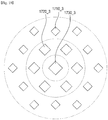
- a method of manufacturing a light emitting element comprises providing a semiconductor structure formed on a substrate, measuring light having different wavelength bands from each other, emitted from the semiconductor structure, to define wavelength regions and forming nanopatterns having different diameters from each other and spaced apart from each other on the semiconductor structure and etching the semiconductor structure to form element rods.
- the wavelength regions may include a first wavelength region from which first light having a first wavelength band is emitted, a second wavelength region from which second light having a second wavelength band shorter than the first wavelength band is emitted, and a third wavelength region from which third light having a third wavelength band shorter than the second wavelength band is emitted.
- the nanopattern having a large diameter may be formed on the wavelength region as the wavelength band of light emitted from the wavelength region decreases.
- the nanopatterns may include a first naopattern, a second nanopattern having a larger diameter than the first nanopattern, and a third nanopattern having a larger diameter than the second nanopattern and the first nanopattern may be formed on the first wavelength region, the second nanopattern may be formed on the second wavelength region, and the third nanopattern may be formed on the third wavelength region.
- the element rods may include a first element rod formed in a region overlapping the first wavelength region, a second element rod formed in a region overlapping the second wavelength region, and a third element rod formed in a region overlapping the third wavelength region.
- the second element rod may be larger in diameter than the first element rod, but smaller in diameter than the third element rod, and the first element rod, the second element rod, and the third element rod may emit light of substantially the same wavelength band.
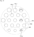
- the third wavelength region may be disposed at a center of the semiconductor structure, the second wavelength region is disposed to surround an outer surface of the third wavelength region, and the first wavelength region may be disposed to surround an outer surface of the second wavelength region.
- the semiconductor structure may include a first axis traversing the center of the semiconductor structure, the diameter of the nanopattern may increase from one end of the first axis toward the center of the semiconductor structure, and the diameter of the nanopattern may decrease from the center of the semiconductor structure toward the other end of the first axis.
- the semiconductor structure may include a second axis traversing the center of the semiconductor structure, the first wavelength region may be disposed at one end of the second axis, the second wavelength region may partially surround an outer surface of the first wavelength region and extends in a direction of the other end of the second axis, and the third wavelength region may partially surround an outer surface of the second wavelength region and extends to the other end of the second axis.
- the diameter of the at least one nanopattern disposed along the second axis may increase from one end of the second axis toward the other end thereof.
- a method of manufacturting a light emitting element comprises providing a substrate and a semiconductor structure disposed on the substrate and including a first conductive semiconductor layer, an active material layer, and a second conductive semiconductor layer, forming an etching mask layer formed on the semiconductor structure and one or more etching pattern layers formed on the etching mask layer, having different diameters from each other, and spaced apart from each other, etching the semiconductor structure in a direction perpendicular to the substrate along a region where the nanopatterns are spaced apart from each other to form element rods; and separating the element rods from the substrate to form light emitting elements.
- the nanopatterns may include a first naopattern, a second nanopattern having a larger diameter than the first nanopattern, and a third nanopattern having a larger diameter than the second nanopattern.
- the light emitting elements may include a first light emitting element having a diameter equal to the diameter of the first nanopattern, a second light emitting element having a diameter equal to the diameter of the second nanopattern, and a third light emitting element having a diameter equal to the diameter of the third nanopattern.
- a difference in diameter between the first light emitting element and the second light emitting element may be in a range of 2% to 16% the diameter of the second light emitting element.
- An interval between the one or more nanopatterns spaced apart from each other may be in a range of 2.5 times to 3.5 times the diameter of each of the nanopatterns.
- the nanopattern may have a circular shape or a polygonal shape.
- a separation layer may be further provided between the substrate and the first conductive semiconductor layer, and the step of forming the light emitting elements may include a step of removing the separation layer to separate the element rods from the substrate.
- a display device comprises a substrate, at least one first electrode and at least one second electrode extending in a first direction and spaced apart from each other in a second direction different from the first direction on the substrate, at least one light emitting element disposed in a space between the first electrode and the second electrode, a first contact electrode partially covering the first electrode and contacting a first end of the light emitting element and a second contact electrode partially covering the second electrode and contacting a second end of the light emitting element, the second end thereof being located opposite to the first end thereof, wherein the light emitting element includes a first light emitting element and a second light emitting element having a larger diameter than the first light emitting element, and the first light emitting element and the second light emitting element emit light of substantially the same wavelength band.
- a difference in diameter between the first light emitting element and the second light emitting element may be in a range of 2% to 16% the diameter of the second light emitting element.
- the light emitting element may further include a third light emitting element, and the third light emitting element may have a larger diameter than the second light emitting element and emit light of substantially the same wavelength band as the second light emitting element.
- nanopatterns formed on a semiconductor structure have different diameters, so that the wavelength band of light emitted from element rods may be shifted. Accordingly, the plurality of light emitting elements may have different diameters, but may emit light of substantially the same wavelength band.
- FIG. 1 is a plan view of a display device according to an embodiment.
- a display device 10 may include at least one region defined as a pixel PX.
- a plurality of pixels PX may be arranged in a display unit of the display device 10 to emit light of a specific wavelength band to the outside of the display device 10.
- FIG. 1 illustrates three pixels PX1, PX2, and PX3, it is obvious that the display device 10 includes a larger number of pixels.
- the drawings show a plurality of pixels PX arranged only in one direction, for example, in a first direction D1, the plurality of pixels PX may be arranged in a second direction D2 intersecting the first direction D1.
- the pixels PX shown in FIG. 1 may be divided into a plurality of pixels to allow each of the plurality of pixels to constitute one pixel PX.
- the pixels may be arranged in a vertical direction (or second direction D2) or may be arranged in a zigzag form, instead of being arranged only in the first direction D1 in parallel as shown in FIG. 1 .
- the display device 10 may include a light emitting area where light emitting elements 300 are arranged to emit light of a specific color, and a non-light emitting area defined as an area other than the light emitting area.
- the non-light emitting area may be covered by specific members not to be viewed from the outside.
- the non-light emitting area may be provided with various members for driving the light emitting elements 300 arranged in the light emitting area.
- the non-light emitting area may be provided with a wiring for applying an electrical signal to the light emitting area, a circuit unit, a driving unit, and the like.
- the present invention is not limited thereto.
- Each of the plurality of pixels may include at least one light emitting element 300 emitting light of a specific wavelength band to display a color.
- the light emitted from the light emitting element 300 may be viewed from the outside of the display device 10.
- light emitting elements 300 emitting light of different colors from each other may be provided for each of the pixels PX expressing different colors from each other.
- the first pixel PX1 expressing a red color may include a light emitting element 300 emitting red light
- the second pixel PX2 expressing a green color may include a light emitting element 300 emitting green light
- the third pixel PX3 expressing a blue color may include a light emitting element 300 emitting blue light.
- pixels PX expressing different colors from each other may include light emitting elements 300 emitting light of the same color (for example, blue), and the colors of the respective pixels PX may be expressed by providing a wavelength conversion layer or a color filter on a light emitting path.
- the present invention is not limited thereto, and in some cases, adjacent pixels PX may emit light of the same color.
- the display device 10 may include a plurality of electrodes 210 and 220 and a plurality of light emitting elements 300. At least a part of the each of the electrodes 210 and 220 may be disposed in each pixel PX, electrically connected to the light emitting elements 300, and apply electrical signals to the light emitting elements to allow the light emitting elements to emit light of a specific color.
- each of the electrodes 210 and 220 may be used to form an electric field in the pixel PX in order to align the light emitting elements 300.
- aligning the light emitting elements 300 emitting light of different colors from each other in the plurality of pixels PX, it is required to accurately align the light emitting elements 300 for each pixel PX.
- aligning the light emitting elements 300 using dielectrophoresis a solution containing the light emitting elements 300 is applied onto the display device 10, an AC power is applied to the solution to form a capacitance caused by an electric field, and thus the light emitting elements 300 may be aligned by a dielectrophoretic force.
- the plurality of electrodes 210 and 220 may include a first electrode 210 and a second electrode 220.
- the first electrode 210 may be a pixel electrode separated for each pixel PX
- the second electrode 220 may be a common electrode connected in common along the plurality of pixels PX.
- Any one of the first electrode 210 and the second electrode 220 may be an anode electrode of the light emitting element 300, and the other thereof may be a cathode electrode of the light emitting element 300.
- the present invention is not limited to this case, and may have an opposite case.
- the first electrode 210 and the second electrode 220 may include electrode stem portions 210S and 220S extending in a first direction D1 and electrode branch portions 210B and 220B extending in a second direction D2 intersecting the first direction D1 and branched from the electrode stem portions 210S and 220S, respectively.
- the first electrode 210 may include a first electrode stem portion 210S extending in the first direction D1 and at least one first electrode branch portion 210B branched from the first electrode stem portion 210S and extending in the second direction D2.
- one end of the first electrode stem portion 210S may be connected to a signal application pad, and the other end thereof may extend in the first direction D1 but electrically separated between the pixels PX.
- the signal application pad may be connected to the display device or an external power source to apply an electrical signal to the first electrode stem portion 210S or apply an AC power thereto at the time of aligning the light emitting elements 300.
- the first electrode stem portion 210S of any one pixel is placed on substantially the same line as the first electrode stem portion 210S of a neighboring pixel belonging to the same row (for example, adjacent in the first direction D1.
- the first electrode stem portion 210S of one pixel is terminated with both ends thereof being spaced apart from each other between the pixels PX, whereas the first electrode stem portion 210S of the neighboring pixel may be aligned with the extension line of the first electrode stem portion 210S of the one pixel.
- Such an arrangement of the first electrode stem portions 210S may be performed by forming one stem electrode during a manufacturing process, performing a process of aligning the light emitting elements 300, and then disconnecting the stem electrode using a laser. Accordingly, the first electrode stem portion 210S disposed in each pixel PX may apply different electrical signals from each other to the respective pixels PX, and the respective pixels PX may be driven separately from each other.
- the first electrode branch portion 210B may be branched from at least a part of the first electrode stem portion 210S and extended in the second direction D2, but may be terminated with being spaced apart from the second electrode stem portion 220S disposed to face the first electrode stem portion 210S. That is, one end of the first electrode branch portion 210B may be connected to the first electrode stem portion 210S, and the other end thereof may be disposed in the pixel PX with it being spaced apart from the second electrode stem portion 220S. Since the first electrode branch portion 210B is connected to the first electrode stem portion 210S electrically separated for each pixel PX, the first electrode branch portion 210B may receive different electrical signals from each other for each pixel PX.
- first electrode branch portions 210B may be disposed for each pixel PX. Although it is shown in FIG. 1 that two first electrode branch portions 210B are disposed and the second electrode branch portion 220B is disposed therebetween, the present invention is not limited thereto, and a larger number of first electrode branch portions 210B may be disposed. In this case, the first electrode branch portions 210B may be alternately spaced apart from the plurality of second electrode branch portions 220B, and a plurality of light emitting elements 300 may be disposed therebetween. In some embodiments, the second electrode branch portion 220B is disposed between the first electrode branch portions 210B, so that each pixel PX may have a symmetrical structure with respect to the second electrode branch portion 220B. However, the present invention is not limited thereto.
- the second electrode 220 may include a second electrode stem portion 220S extending in the first direction D1, spaced apart from the first electrode stem portion 210S and facing the first electrode stem portion 210S and at least one second electrode branch portion 220B branched from the second electrode stem portion 220S, extending in the second direction D2, spaced apart from the first electrode branch portion 210B and facing the first electrode branch portion 210B.
- a second electrode stem portion 220S extending in the first direction D1, spaced apart from the first electrode stem portion 210S and facing the first electrode stem portion 210S and at least one second electrode branch portion 220B branched from the second electrode stem portion 220S, extending in the second direction D2, spaced apart from the first electrode branch portion 210B and facing the first electrode branch portion 210B.
- one end of the second electrode stem portion 220S may also be connected to a signal application pad.
- the other end of the second electrode stem portion 220S may extend to the plurality of pixels PX adjacent in the first direction D1. That is
- both ends of the second electrode stem portion 220S of any one pixel may be connected to one end of the second electrode stem portion 220S of a neighboring pixel PX between the respective pixels PX, so that the same electrical signal may be applied to the respective pixels PX.
- the second electrode branch portion 220B may be branched from at least a part of the second electrode stem portion 220S and extended in the second direction D2, but may be terminated with it being spaced apart from the first electrode stem portion 210S. That is, one end of the second electrode branch portion 220B may be connected to the second electrode stem portion 220S, and the other end thereof may be disposed in the pixel PX with it being spaced apart from the first electrode stem portion 210S. Since the second electrode branch portion 220B is connected to the second electrode stem portion 220S electrically connected for each pixel PX, the second electrode branch portion 220B may receive the same electrical signal for each pixel PX.
- the second electrode branch portion 220B may be disposed to be spaced apart from the first electrode branch portion 210B and face the first electrode branch portion 210B.
- the first electrode branch portion 210B and the second electrode branch portion 220B may extend in directions opposite to each other.
- the first electrode branch portion 210B extends in one direction of the second direction D2
- the second electrode branch portion 220B extends in the other direction of the second direction D2, so that one ends of the respective branch portions may be disposed in directions opposite to each other with respect to the center of the pixel PX.
- first electrode stem portion 210S and the second electrode stem portion 220S may be disposed to be spaced apart from each other in the same direction with respect to the center of the pixel PX.
- first electrode branch portion 210B and the second electrode branch portion 220B respectively branched from the first electrode stem portion 210S and the second electrode stem portion 220S, may extend in the same direction.
- each second electrode branch portion 220B is disposed in each pixel PX, the present invention is not limited thereto, and a larger number of second electrode branch portions 220B may be disposed.
- a plurality of light emitting elements 300 may be arranged between the first electrode branch portion 210B and the second electrode branch portion 220B. One ends of at least some of the plurality of light emitting elements 300 may be electrically connected to the first electrode branch portion 210B, and the other ends thereof may be electrically connected to the second electrode branch portion 220B.
- the plurality of light emitting elements 300 may be spaced apart from each other in the second direction D2 and may be aligned substantially parallel to each other.
- the interval between the light emitting elements 300 is not particularly limited.
- the plurality of light emitting elements 300 are arranged adjacent to each other to form a group, the plurality of light emitting elements 300 may form a group in a state spaced apart at a predetermined interval, and the plurality of light emitting elements 300 may have non-uniform density and may be oriented and aligned in one direction.
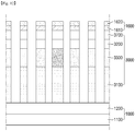
- the plurality of light emitting elements 300 may include light emitting elements having different diameters from each other, for example, a first light emitting element 301, a second light emitting element 302, and a third light emitting element 303.
- the light emitting element 300 may emit light of different wavelength bands according to the composition of an element active layer 330 and the kind of an active material.
- the element active layer 330 grown on the same wafer substrate may have a difference in composition according to a spatial position, and may have a deviation in a wavelength band of partially emitted light.
- the second light emitting element 302 having an arbitrary diameter emits second light L2 having a second wavelength band
- other light emitting elements grown on the same wafer substrate may have a difference in composition of the element active layer 330 according to the spatial position of the wafer substrate.
- light of a different wavelength band for example, first light L1 of a first wavelength band longer than a second wavelength band or third light L3 of a third wavelength band shorter than the second wavelength band may be emitted according to a difference in the composition of the element active layer 330.
- the light emitting elements 300 grown on the same wafer substrate have the same diameter, deviations in emission wavelengths may occur due to a difference in the composition of the element active layer 330.
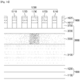
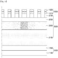
- etching pattern layers 1700 (shown in FIG. 8 ) having different diameters may be formed, thereby forming element rods ROD (shown in FIG. 12 ) having different diameters from each other according to the difference in composition of the element active layer 330, and the display device 10 according to an embodiment may include light emitting elements 300 having different diameters from each other and emitting light of substantially the same wavelength band. Details thereof will be described later.
- Contact electrodes 260 may be disposed on the first electrode branch portion 210B and the second electrode branch portion 220B, respectively.
- the plurality of contact electrodes 260 may be arranged to be extended in the second direction D2 and spaced apart from each other in the first direction D1. Each of the contact electrodes 260 may be in contact with at least one end of the light emitting element 300, and may be in contact with the first electrode 210 or the second electrode 220 to receive an electrical signal. Thus, the contact electrode 260 may transmit the electrical signal received from the first electrode 210 or the second electrode 220 to the light emitting element 300.
- the contact electrodes 260 may be disposed on the electrode branch portions 210B and 220B to partially cover the electrode branch portions 210B and 220B, and may include a first contact electrode 261 and a second contact electrode 262, each contacting one end or the other end of the light emitting element 300.
- the first contact electrode 261 may be disposed on the first electrode branch portion 210B, and may be in contact with one end of the light emitting element 300 electrically connected to the first electrode 210.
- the second contact electrode 262 may be disposed on the second electrode branch portion 220B, and may be in contact with the other end of the light emitting element 300 electrically connected to the second electrode 220.
- both ends of the light emitting element 300 electrically connected to the first electrode branch portion 210B or the second electrode branch portion 220B may be a conductive semiconductor layer doped with an n-type dopant or a p-type dopant.
- the other end of the light emitting element 300 electrically connected to the second electrode branch portion 220B may be a conductive semiconductor layer doped with an n-type dopant.
- the present invention is not limited thereto.
- the first contact electrode 261 and the second contact electrode 262 may be disposed on the first electrode branch 210B and the second electrode branch 220B to partially cover the first electrode branch 210B and the second electrode branch 220B, respectively. As shown in FIG. 1 , the first contact electrode 261 and the second contact electrode 262 may be disposed to be extended in the second direction D2, spaced apart from each other and facing each other. However, one end of each of the first contact electrode 261 and the second contact electrode 262 may be terminated to partially expose one end of each of the electrode branch portions 210B and 220B.
- each of the first contact electrode 261 and the second contact electrode 262 may be terminated in a state where they are spaced apart from each other so as not to overlap each of the electrode stem portions 210S and 220S.
- the present invention is not limited thereto, and the other end of each of the first contact electrode 261 and the second contact electrode 262 may cover each of the electrode branch portions 210B and 220B.
- the first electrode stem portion 210S and the second electrode stem portion 220S may be electrically connected to a thin film transistor 120 or a power supply wiring 161, which will be described later, through contact holes, for example, a first electrode contact hole CNTD and a second electrode contact hole CNTS, respectively.
- contact holes for example, a first electrode contact hole CNTD and a second electrode contact hole CNTS, respectively.
- the present invention is not limited thereto.
- the second electrode stem portion 220S may extend to be electrically connected to the adjacent pixel PX, in some embodiments, the second electrode stem portion 220S may be electrically connected to a thin film transistor through one contact hole.
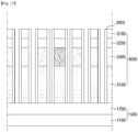
- FIG. 2 is a cross-sectional view taken along the lines I-I', II-II', and III-III' of FIG. 1 . Although FIG. 2 shows only one pixel PX, it may be applied to other pixels as well. FIG. 2 shows a cross-section across one end and the other end of any light emitting element 300.
- the display device 10 may include a substrate 110, thin film transistors 120 and 140 disposed on the substrate 110, and electrodes 210 and 220 and a light emitting element 300 disposed over the thin film transistors 120 and 140.
- the thin film transistors may include a first thin film transistor 120 and a second thin film transistor 140, which may be a driving transistor and a switching transistor, respectively.
- Each of the thin film transistors 120 and 140 may include an active layer, a gate electrode, a source electrode, and a drain electrode.
- the first electrode 210 may be electrically connected to the drain electrode of the first thin film transistor 120.
- the substrate 110 may be an insulating substrate.
- the substrate 110 may be made of an insulating material such as glass, quartz, or a polymer resin.
- the polymer resin may include polyethersulphone (PES), polyacrylate (PA), polyarylate (PAR), polyetherimide (PEI), polyethylene naphthalate (PEN), polyethylene terephthalate (PET), polyphenylene sulfide (PPS), polyallylate, polyimide (PI), polycarbonate (PC), cellulose triacetate (CAT), cellulose acetate propionate (CAP), and combinations thereof.
- the substrate 110 may be a rigid substrate, but may be a flexible substrate capable of bending, folding, rolling, or the like.
- a buffer layer 115 may be disposed on the substrate 110.
- the buffer layer 115 may prevent the diffusion of impurity ions, may prevent the penetration of moisture or external air, and may perform a surface planarization function.
- the buffer layer 115 may include silicon nitride, silicon oxide, or silicon oxynitride.
- a semiconductor layer is disposed on the buffer layer 115.
- the semiconductor layer may include a first active layer 126 of the first thin film transistor 120, a second active layer 146 of the second thin film transistor 140, and an auxiliary layer 163.
- the semiconductor layer may include polycrystalline silicon, monocrystalline silicon, an oxide semiconductor, or the like.
- a first gate insulating layer 170 is disposed on the semiconductor layer.
- the first gate insulating layer 170 covers the semiconductor layer.
- the first gate insulating layer 170 may function as a gate insulating film of the thin film transistor.
- the first gate insulating layer 170 may include silicon oxide, silicon nitride, silicon oxynitride, aluminium oxide, tantalum oxide, hafnium oxide, zirconium oxide, titanium oxide, or the like. These compounds may be used alone or in combination with each other.
- a first conductive layer is disposed on the first gate insulating layer 170.
- the first conductive layer may include a first gate electrode 121 disposed on the first active layer 126 of the first thin film transistor 120, a second gate electrode 141 disposed on the second active layer 146 of the second thin film transistor 140, and a power supply wiring 161 disposed on the auxiliary layer 163, with the first gate insulating layer 170 therebetween.
- the first conductive layer may include at least one metal selected from molybdenum (Mo), aluminium (Al), platinum (Pt), palladium (Pd), silver (Ag), magnesium (Mg), gold (Au), nickel (Ni), neodymium (Nd), iridium (Ir), chromium (Cr), calcium (Ca), titanium (Ti), tantalum (Ta), tungsten (W), and copper (Cu).
- the first conductive layer may be a single-layer film or a multilayer film.
- a second gate insulating layer 180 is disposed on the first conductive layer.
- the second gate insulating layer 180 may be an interlayer insulating film.
- the second gate insulating layer 180 may include an inorganic insulating material such as silicon oxide, silicon nitride, silicon oxynitride, hafnium oxide, aluminium oxide, titanium oxide, tantalum oxide, or zinc oxide.
- a second conductive layer is disposed on the second gate insulating layer 180.
- the second conductive layer includes a capacitor electrode 128 disposed on the first gate electrode 121 with the second gate insulating layer 180 therebetween.
- the capacitor electrode 128 may constitute a storage capacitor together with the first gate electrode 121.
- the second conductive layer may include at least one metal selected from molybdenum (Mo), aluminium (Al), platinum (Pt), palladium (Pd), silver (Ag), magnesium (Mg), gold (Au), nickel (Ni), neodymium (Nd), iridium (Ir), chromium (Cr), calcium (Ca), titanium (Ti), tantalum (Ta), tungsten (W), and copper (Cu).
- Mo molybdenum
- Al aluminium
- platinum (Pt) palladium
- silver Ag
- gold Au
- Ni nickel
- Ni neodymium
- Ir iridium
- Cr chromium
- Ca calcium
- Ti titanium
- Ta tantalum
- W tungsten
- Cu copper
- the interlayer insulating layer 190 is disposed on the second conductive layer.
- the interlayer insulating layer 190 may be an interlayer insulating film. Moreover, the interlayer insulating layer 190 may perform a surface planarization function.
- the interlayer insulating layer 190 may include an organic insulating material such as polyacrylate resin, epoxy resin, phenolic resin, polyamide resin, polyimide rein, unsaturated polyester resin, polyphenyleneether resin, polyphenylenesulfide resin, or benzocyclobutene (BCB).
- a third conductive layer is disposed on the interlayer insulating layer 190.
- the third conductive layer includes a first drain electrode 123 and first source electrode 124 of the first thin film transistor 120, a second drain electrode 143 and second source electrode 144 of the second thin film transistor 140, and a power supply electrode 162 disposed on the power supply wiring 161.
- Each of the first source electrode 124 and the first drain electrode 123 may be electrically connected to the first active layer 126 through a first contact hole 129 penetrating the interlayer insulating layer 190 and the second gate insulating layer 180.
- Each of the second source electrode 144 and the second drain electrode 143 may be electrically connected to the second active layer 146 through a second contact hole 149 penetrating the interlayer insulating layer 190 and the second gate insulating layer 180.
- the power supply electrode 162 may be electrically connected to the power supply wiring 161 through a third contact hole 169 penetrating the interlayer insulating layer 190 and the second gate insulating layer 180.
- the third conductive layer may include at least one metal selected from molybdenum (Mo), aluminium (Al), platinum (Pt), palladium (Pd), silver (Ag), magnesium (Mg), gold (Au), nickel (Ni), neodymium (Nd), iridium (Ir), chromium (Cr), calcium (Ca), titanium (Ti), tantalum (Ta), tungsten (W), and copper (Cu).
- the third conductive layer may be a single-layer film or a multilayer film.
- the third conductive layer may be formed of a laminate structure of Ti / Al / Ti, Mo / Al / Mo, Mo / AlGe / Mo, or Ti / Cu.
- the insulating substrate layer 200 is disposed on the third conductive layer.
- the insulating substrate layer 200 may include an organic insulating material such as polyacrylate resin, epoxy resin, phenolic resin, polyamide resin, polyimide rein, unsaturated polyester resin, polyphenyleneether resin, polyphenylenesulfide resin, or benzocyclobutene (BCB).
- the surface of the insulating substrate layer 300 may be flat.
- a plurality of partition walls 410 and 420 may be disposed on the insulating substrate layer 200.
- the plurality of partition walls 410 and 420 are disposed to be spaced apart from each other and face each other in each of the pixels PX, and the first electrode 210 and the second electrode 220 may be disposed on the partition walls 410 and 420 spaced apart from each other, for example, a first partition wall 410 and a second partition wall 420.
- FIG. 1 shows a case where three partition walls 410 and 420, specifically, two first partition walls 410 and one second partition wall 420 are disposed in one pixel PX, and thus two first electrodes 210 and one second electrode 220 are disposed.
- FIG. 2 shows only a cross-sectional view of one first partition wall 410 and one second partition wall 420, and the arrangement structure thereof may be equally applied to other first partition walls 410 not shown in FIG. 2 .
- the number of partition walls 410 and 420 is not limited thereto.
- a larger number of partition walls 410 and 420 may be disposed in one pixel PX, and thus a larger number of first and second electrodes 210 and 220 may be disposed.
- the partition walls 410 and 420 may include at least one first partition wall 410 on which the first electrode 210 is disposed, and at least one second partition wall 420 on which the second electrode 220 is disposed.
- the first partition wall 410 and the second partition wall 420 may be disposed to be spaced apart from each other and face each other, and the plurality of partition walls may be alternately arranged in one direction.
- two first partition walls 410 may be disposed to be spaced apart from each other, and one second partition wall 420 may be disposed between the spaced first partition walls 410.
- the first electrode 210 and the second electrode 220 may include the electrode stem portions 210S and 220S and the electrode branch portions 210B and 220B, respectively. It may be understood that the first electrode branch portion 210B and the second electrode branch portion 220B are disposed on the first partition wall 410 and the second partition wall 420, respectively.
- the plurality of partition walls 410 and 420 may be made of substantially the same material, and thus may be formed in one process. In this case, the partition walls 410 and 420 may form one lattice pattern.
- the partition walls 410 and 420 may include polyimide (PI).
- the plurality of partition walls 410 and 420 may be disposed at the boundary between the respective pixels PX to distinguish them from each other.
- the electrodes 210 and 220 may not be disposed on the partition walls 410 and 420 disposed at the boundary between the respective pixels PX.
- These partition walls may be arranged in a substantially lattice pattern together with the first partition wall 410 and second partition wall 420 described above.
- At least some of the plurality of partition walls 410 and 420 disposed at the boundary between the respective pixels PX may be disposed to cover the electrode lines of the display panel 10.
- Each of the plurality of partition walls 410 and 420 may have a structure in which at least a part thereof protrudes from the insulating substrate layer 200.
- Each of the partition walls 410 and 420 may protrude upward with respect to a plane on which the light emitting element 300 is disposed, and at least a part of the protruding portion may have an inclination.
- Each of the partition walls 410 and 420 protruding with an inclination may reflect light incident on reflective layers 211 and 221 disposed thereon, which will be described later. Light directed from the light emitting element 300 to the reflective layers 211 and 221 may be reflected and transmitted to the outside of the display device 10, for example, above the partition walls 410 and 420.
- each of the protruded partition walls 410 and 420 is not particularly limited. Although it is shown in FIG. 2 that each of the partition walls 410 and 420 has a protruding structure having an angled corner shape in which both side surfaces are flat and one upper side is flat, the present invention is not limited thereto, and each of the partition walls 410 and 420 may have a structure protruding in a curved shape.
- the reflective layers 211 and 221 may be disposed on the plurality of partition walls 410 and 420.
- the first reflective layer 211 covers the first partition wall 410, and a part thereof is electrically connected to the first drain electrode 123 of the first thin film transistor 120 through a fourth contact hole 319_1 penetrating the insulating substrate layer 200.
- the second reflective layer 221 covers the second partition wall 420, and a part thereof is electrically connected to the power supply electrode 162 through a fifth contact hole 319_2 penetrating the insulating substrate layer 200.
- the first reflective layer 211 may be electrically connected to the first drain electrode 123 of the first thin film transistor 120 through the fourth contact hole 319_1 in the pixel PX. Therefore, the first thin film transistor 120 may be disposed in a region overlapping the pixel PX. It is shown in FIG. 1 that it is electrically connected to the first thin film transistor 120 through the first electrode contact hole CNTD disposed on the first electrode stem portion 210S. That is, the first electrode contact hole CNTD may be the fourth contact hole 319_1.
- the second reflective layer 221 may also be electrically connected to the power supply electrode 162 through the fifth contact hole 319_2 in the pixel PX. It is shown in FIG. 2 that the second reflective layer 221 is electrically connected to the power supply electrode 162 through the fifth contact hole 319_2 in one pixel PX. It is shown in FIG. 1 that the second electrode 220 of each pixel PX is electrically connected to the power supply wiring 161 through the plurality of second electrode contact holes CNTS on the second electrode stem portion 220S. That is, the second electrode contact hole CNTS may be the fifth contact hole 319_2.
- the first electrode contact hole CNTD and the second electrode contact hole CNTS are disposed on the first electrode stem portion 210S and the second electrode stem portion 220S, respectively. Accordingly, it is shown in FIG. 2 that, in the cross-sectional view of the display device 10, the first electrode 210 and the second electrode 220 are electrically connected to the first thin film transistor 120 or the power supply wiring 161 through the fourth contact hole 319_1 and the fifth contact hole 319_2, respectively, in a region spaced apart from the partition walls 410 and 420 where the first electrode branch portion 210B and the second electrode branch portion 220B are disposed.
- the present invention is not limited thereto.
- the second electrode contact hole CNTS may be disposed at various positions even on the second electrode stem portion 220S, and in some cases, the second electrode contact hole CNTS may be disposed on the second electrode branch portion 220B.
- the second reflective layer 221 may be connected to one second electrode contact hole CNTS or one fifth contact hole 319_2 in a region other than the pixel PX.
- the display device 10 may include an area other than the light-emitting area where the light emitting elements 300 are disposed, for example, a non-light emitting area where the light emitting elements 300 are not disposed.
- the second electrodes 220 of each pixel PX are electrically connected to each other through the second electrode stem portion 220S, so as to receive the same electrical signal.
- the second electrode stem portion 220S may be electrically connected to the power supply electrode 162 through one second electrode contact hole CNTS in the non-light emitting area located at the outside of the display device 10. Unlike the display device 10 of FIG. 1 , even when the second electrode stem portion 220S is connected to the power supply electrode 162 through one contact hole, the second electrode stem portion 220S is extended to the adjacent pixel PX and is electrically connected, so that the same electric signal may be applied to the second electrode branch portion 220B of each pixel PX. In the case of the second electrode 220 of the display device 10, the position of the contact hole for receiving an electric signal from the power supply electrode 162 may vary according to the structure of the display device 10.
- each of the reflective layers 211 and 221 may include a high-reflectance material to reflect the light emitted from the light emitting element 300.
- each of the reflective layers 211 and 221 may include a material such as silver (Ag) or copper (Cu), but the present invention is not limited thereto.
- a first electrode layer 212 and a second electrode layer 222 may be disposed on the first reflective layer 211 and the second reflective layer 221, respectively.
- the first electrode layer 212 is disposed directly on the first reflective layer 211.
- the first electrode layer 212 may have substantially the same pattern as the first reflective layer 211.
- the second electrode layer 222 is disposed directly on the second reflective layer 221 and spaced apart from the first electrode layer 212.
- the second electrode layer 222 may have substantially the same pattern as the second reflective layer 221.
- the electrode layers 212 and 222 may cover the underlying reflective layers 211 and 221, respectively. That is, the electrode layers 212 and 222 may be formed to be larger than the reflective layers 211 and 221 to cover the side surfaces of ends of the reflective layers 211 and 221.
- the present invention is not limited thereto.
- the first electrode layer 212 and the second electrode layer 222 may transmit the electric signals transmitted to the first reflective layer 211 and second reflective layer 221 connected to the first thin film transistor 120 or the power supply electrode 162 to contact electrodes to be described later.
- the electrode layers 212 and 222 may include a transparent conductive material.
- the electrode layers 212 and 222 may include a material such as indium tin oxide (ITO), indium zinc oxide (IZO), or indium tin-zinc oxide (ITZO), but the present invention is not limited thereto.
- the reflective layers 211 and 221 and the electrode layers 212 and 222 may have a structure in which a transparent conductive layer such as ITO, IZO, or ITZO and a metal layer such as silver or copper are laminated one or more layers.
- the reflective layers 211 and 221 and the electrode layers 212 and 222 may have a laminate structure of ITO / silver (Ag) / ITO.
- the first electrode 210 may protrude to a region extending from both ends of the first partition wall 410, and thus the first electrode 210 may be in contact with the insulating substrate layer 200 in the protruding region.
- the second reflective layer 221 and the second electrode layer 222, which are disposed on the second partition wall 420, constitute the second electrode 220.
- the second electrode 220 may protrude to a region extending from both ends of the second partition wall 420, and thus the second electrode 220 may be in contact with the insulating substrate layer 200 in the protruding region.
- the first electrode 210 and the second electrode 220 may be disposed to cover the entire region of the first partition wall 410 and the entire region of the second partition wall 420, respectively. However, as described above, the first electrode 210 and the second electrode 220 are spaced apart from each other and face each other. As will be described later, a first insulating material layer 510 may be disposed between the first electrode 210 and second electrode 220 spaced apart from each other, and the light emitting element 300 may be disposed on the first insulating material layer 510.
- the first reflective layer 211 may receive a driving voltage from the first thin film transistor 120
- the second reflective layer 221 may receive a power supply voltage from the power supply wiring 161, so that the first electrode 210 and the second electrode 220 receive a driving voltage and a power supply voltage, respectively.
- the first electrode 210 may be electrically connected to the first thin film transistor 120
- the second electrode 220 may be electrically connected to the power supply wiring 161.
- the first contact electrode 261 and the second contact electrode 262 disposed on the first electrode 210 and the second electrode 220 may receive the driving voltage and the power supply voltage.
- the driving voltage and the power supply voltage are transmitted to the light emitting element 300, and a predetermined current flows through the light emitting element 300, so as to emit light.
- the first insulating material layer 510 is disposed on the first electrode 210 and the second electrode 220 to partially cover them.
- the first insulating material layer 510 may be disposed so as to cover most of the upper surfaces of the first electrode 210 and the second electrode 220, and may exposed a part of the first electrode 210 and a part of the second electrode 220.
- the first insulating material layer 510 may be disposed in a space between the first electrode 210 and second electrode 220.
- the first insulating material layer 510 may have an island shape or a linear shape formed along a space between the first electrode branch portion 210B and the second electrode branch portion 220B in a plan view.
- the first insulating material layer 510 is disposed in a space between one first electrode 210 (for example, the first electrode branch portion 210B) and one second electrode 220 (for example, the second electrode branch portion 220B).
- the first insulating material layer 510 may be also disposed between one first electrode 210 and another second electrode 220 or between one second electrode 220 and another first electrode 210.
- the first insulating material layer 510 may be disposed on sides opposite to the facing sides of the first electrode 210 and the second electrode 220 so as to partially cover them. That is, the first insulating material layer 510 may be disposed so as to expose the centers of the first electrode 210 and the second electrode 220.
- the light emitting element 300 is disposed on the first insulating material layer 510.
- the first insulating material layer 510 may be disposed between the light emitting element 300 and the insulating substrate layer 200.
- the lower surface of the first insulating material layer 510 may be in contact with the insulating substrate layer 200, and the light emitting element 300 may be disposed on the upper surface of the first insulating material layer 510.
- both side surfaces of the first insulating material layer 510 may be in contact with the first electrode 210 and the second electrode 220 to electrically insulate them from each other.
- the first insulating material layer 510 may overlap a part of a region on each of the electrodes 210 and 220, for example, a part of a region protruding in a direction in which the first electrode 210 and the second electrode 220 face each other.
- the first insulating material layer 510 may also be disposed in a region where the inclined side surface and flat upper surfaces of each of the partition walls 410 and 420 overlap each of the electrodes 210 and 220.
- the first insulating material layer 510 may cover each end protruding in a direction in which the first electrode 210 and the second electrode 220 face each other.
- the first insulating material layer 510 may be in contact with a part of the lower surface of the insulating substrate layer 200, and may be in contact with the side surface of each of the electrodes 210 and 220 and a part of the lower surface of each of the electrodes 210 and 220. Therefore, the first insulating material layer 510 may protect the region overlapping each of the electrodes 210 and 220, and electrically insulate them from each other. Further, the first insulating material layer 510 may prevent the first conductive semiconductor layer 310 and second conductive semiconductor layer 320 of the light emitting element 300 from being in direct contact with other substrates to prevent the damage of the light emitting element 300.
- the present invention is not limited thereto, and the first insulating material layer 510 may be disposed only in the region overlapping the inclined surfaces of the partition walls 410 and 420 among the regions on the first electrode 210 and the second electrode 220.
- the lower of the first insulating material layer 510 is terminated at the inclined surface of each of the partition walls 410 and 420, and each of the electrodes 210 and 220 disposed on a part of the inclined surface of each of the partition walls 410 and 420 is exposed to be in contact with the contact electrode 260.
- the first insulating material layer 510 may be disposed such that both ends of the light emitting element 300 are exposed. Accordingly, the contact electrode 260 may be in contact with the exposed upper surface of each of the electrodes 210 and 220 and both ends of the light emitting element 300, and the contact electrode 260 may transmit an electrical signal applied to the first electrode 210 and the second electrode 220 to the light emitting element 300.
- At least one light emitting element 300 may be disposed between the first electrode 210 and the second electrode 220. Although it is shown in FIG. 2 that one light emitting element 300 is disposed between the first electrode 210 and the second electrode 220 in a cross-section, it is obvious that, as shown in FIG. 1 , the plurality of light emitting elements 300 may be arranged in a different direction (for example, second direction D2) on a plane.
- one end of the light emitting element 300 may be electrically connected to the first electrode 210, and the other end thereof may be electrically connected to the second electrode 220. Both ends of the light emitting element 300 may be in contact with the first contact electrode 261 and the second contact electrode 262, respectively.
- the present invention is not limited thereto. As described above, the light emitting elements 300 emitting light of different colors from each other may be arrange in one pixel PX.
- the light emitting element 300 may be a light emitting diode.
- the light emitting element 300 may be a nanostructure whose size is generally nanometer.
- the light emitting element 300 may be an inorganic light emitting diode including an inorganic material.
- the light emitting element 300 is an inorganic light emitting diode, when a light emitting material having an inorganic crystal structure is disposed between two electrodes facing each other and an electric field is formed in the light emitting material in a specific direction, the inorganic light emitting diode may be aligned between the two electrodes in which a specific polarity is formed.
- the light emitting element 300 may include a first conductive semiconductor layer 310, an element active material layer 330, a second conductive semiconductor layer 320, and an electrode material layer 370, which are sequentially laminated, and an insulating layer 380 surrounding the outer peripheral surfaces of these layers.
- the first conductive semiconductor layer 310, the element active material layer 330, the second conductive semiconductor layer 320, and the electrode material layer 370 are arranged in a direction horizontal to the insulating substrate layer 200.
- the light emitting element 300, in which the plurality of layers are formed may be disposed in a horizontal direction horizontal to the insulating substrate layer 200.
- the present invention is not limited thereto, and the light emitting element 300 may be aligned such that the aforementioned laminating direction is reversed between the first electrode 210 and the second electrode 220.
- FIG. 2 Although it is shown in FIG. 2 that only one light emitting element 300 is disposed, as described above, a plurality of light emitting elements 300 having different diameters from each other may be arranged between the first electrode 210 and the second electrode 220. Details of the light emitting element will be described later.
- the second insulating material layer 520 may be disposed to overlap at least a part of the region on the light emitting element 300.
- the second insulating material layer 520 may protect the light emitting element 300, and may fix the light emitting element 300 between the first electrode 210 and the second electrode 220.
- the second insulating material layer 520 may be disposed to surround the outer surface of the light emitting element 300. That is, like the first insulating material layer 510, the second insulating material layer 520 may be disposed to extend in the second direction D2 along a space between the first electrode branch portion 210B and the second electrode branch portion 220B so as to have an island shape or a linear shape in a plan view.
- a part of the material of the second insulating material layer 520 may be disposed even in a region where the lower surface of the light emitting element 300 is contact with the first insulating material layer 510. This configuration may be formed when the light emitting element 300 is aligned on the first insulating material layer 510 and the second insulating material layer 520 is disposed on the first insulating material layer 510 at the time of manufacturing the display device 10.
- a part of the material of the second insulating material layer 520 penetrates into the voids when the second insulating material layer 520 is formed, so as to form the configuration.
- the second insulating material layer 520 is disposed such that both side surfaces of the light emitting element 300 are exposed. That is, since the length of the second insulating material layer 520 disposed on the upper surface of the light emitting element 300 in the cross-section, measured in the uniaxial direction, is shorter than the length of the light emitting element 300, the second insulating material layer 520 may be recessed inwardly from both side surfaces of the light emitting element 300. Accordingly, the side surfaces of the first insulating material layer 510, the light emitting element 300, and the second insulating material layer 520 may be laminated stepwise. In this case, the contact electrodes 261 and 262 to be described later may be brought into smooth contact with both ends of the light emitting element 300. However, the present invention is not limited thereto, and the length of the second insulating material layer 520 may be matched with the length of the light emitting element 300, so that both sides thereof may be aligned with each other.
- the second insulating material layer 520 may be disposed to cover the first insulating material layer 510 and then patterned in a region where the light emitting element 300 is exposed to be in contact with the contact electrode 260.
- the process of patterning the second insulating material layer 520 may be performed by a general dry etching or wet etching method.
- the first insulating material layer 510 and the second insulating material layer 520 may include materials having different etching selection ratios from each other.
- the first insulating material layer 510 may function as an etching stopper.
- the material of the first insulating material layer 510 is not damaged.
- the first insulating material layer 510 and the light emitting element 300 may form a smooth contact surface at both ends of the light emitting element 300, at which the light emitting element 300 is in contact with the contact electrode 260.
- the first contact electrode 261 disposed on the first electrode 210 and overlapping at least a part of the second insulating material layer 520, and the second contact electrode 262 disposed on the second electrode 220 and overlapping at least a part of the second insulating material layer 520 may be disposed on the second insulating material layer 520.
- the first contact electrode 261 and the second contact electrode 262 may be disposed on the upper surface of the first electrode 210 and the upper surface of the second electrode 220, respectively. Specifically, the first contact electrode 261 and the second contact electrode 262 may be in contact with the first electrode layer 212 and the second electrode layer 222, respectively, in the region where the first insulating material layer 510 is patterned to expose a part of the first electrode 210 and a part of the second electrode 220. Each of the first contact electrode 261 and the second contact electrode 262 may be in contact with one end side surface of the light emitting element 300, for example, the first conductive semiconductor layer 310, the second conductive semiconductor layer 320, or the electrode material layer 370. Thus, the first contact electrode 261 and the second contact electrode 262 may transmit electrical signals applied to the first electrode layer 212 and the second electrode layer 222 to the light emitting element 300.
- the first contact electrode 261 may be disposed on the first electrode 210 to partially cover the first electrode 210, and may be partially in contact with the light emitting element 300, the first insulating material layer 510, and the second insulating material layer 520. One end of the first contact electrode 261 in the direction in which the second contact electrode 262 is disposed may be disposed on the second insulating material layer 520.
- the second contact electrode 262 may be disposed on the second electrode 220 to partially cover the second electrode 220, and may be partially in contact with the light emitting element 300, the first insulating material layer 510, and a third insulating material layer 530. One end of the second contact electrode 262 in the direction in which the first contact electrode 261 is disposed may be disposed on the third insulating material layer 530.
- Areas where the first insulating material layer 510 and the second insulating material layer 520 are disposed to cover the first electrode 210 and the second electrode 220 on the upper surfaces of the first partition wall 410 and the second partition wall 420 may be patterned. Accordingly, the first electrode layer 212 of the first electrode 210 and the second electrode layer 222 of the second electrode 220 are exposed to be electrically connected to the contact electrodes 261 and 262, respectively.
- the first contact electrode 261 and the second contact electrode 262 may be disposed to be spaced apart from each other on the second insulating material layer 520 or the third insulating material layer 530. That is, the first contact electrode 261 and the second contact electrode 262 are in contact with the light emitting element 300 and the second insulating material layer 520 or the third insulating material layer 530 together, but are spaced apart from each other in a lamination direction on the second insulating material layer 520 to be electrically insulated from each other. Accordingly, the first contact electrode 261 and the second contact electrode 262 may receive different powers from the first thin film transistor 120 and the power line 161.
- the first contact electrode 261 may receive a driving voltage applied from the first thin film transistor 120 to the first electrode 210, and the second contact electrode 262 may receive a common power voltage applied from the power line 161 to the second electrode 220.
- the present invention is not limited thereto.
- the contact electrodes 261 and 262 may include a conductive material.
- the contact electrodes 261 and 262 may include ITO, IZO, ITZO, or aluminium (Al).
- the present invention is not limited thereto.
- the contact electrodes 261 and 262 may include the same material as the electrode layers 212 and 222.
- the contact electrodes 261 and 262 may be disposed in substantially the same pattern on the electrode layers 212 and 222 so as to be in contact with the electrode layers 212 and 222.
- the first contact electrode 261 contacting the first electrode layer 212 and the second contact electrode 262 contacting the second electrode layer 222 may receive electrical signals applied from the first electrode layer 212 and the second electrode layer 222 and transmit the electrical signals to the light emitting element 300.
- the third insulating material layer 530 may be disposed on the first contact electrode 261 to electrically insulate the first contact electrode 261 and the second contact electrode 262 from each other.
- the third insulating material layer 530 may be disposed to cover the first contact electrode 261, but may be disposed not to overlap a part of the light emitting element 300 such that the light emitting element 300 is in contact with the second contact electrode 262.
- the third insulating material layer 530 may partially contact the first contact electrode 261, the second contact electrode 262, and the second insulating material layer 520 on the upper surface of the second insulating material layer 520.
- the third insulating material layer 530 may be disposed to cover one end of the first contact electrode 261 on the upper surface of the second insulating material layer 520.
- the third insulating material layer 530 may protect the first contact electrode 261 and electrically insulate the first contact electrode 261 and the second contact electrode 262 from each other.
- One end of the third insulating material layer 530 in the direction in which the second electrode 220 is disposed may be aligned with one side surface of the second insulating material layer 520.
- the third insulating material layer 530 may be omitted in the display device 10. Accordingly, the first contact electrode 261 and the second contact electrode 262 may be disposed on substantially the same plane, and the first contact electrode 261 and the second contact electrode 262 may be electrically insulated from each other by a passivation layer 550 to be described later.
- the passivation layer 550 may be formed on the third insulating material layer 530 and the second contact electrode 262 to function to protect members disposed on the insulating substrate layer 200 from external environments. When the first contact electrode 261 and the second contact electrode 262 are exposed, a problem of disconnection of a contact electrode material due to electrode damage may occur, so that the passivation layer 550 may cover these members. That is, the passivation layer 550 may be disposed to cover the first electrode 210, the second electrode 220, the light emitting element 300, and the like. As described above, when the third insulating material layer 530 is omitted, the passivation layer 550 may be formed on the first contact electrode 261 and the second contact electrode 262. In this case, the passivation layer 550 may electrically insulate the first contact electrode 261 and the second contact electrode 262 from each other.
- first insulating material layer 510, second insulating material layer 520, third insulating material layer 530, and passivation layer 550 may include an inorganic insulating material.
- first insulating material layer 510, the second insulating material layer 520, the third insulating material layer 530, and the passivation layer 550 may include an inorganic insulating material such as silicon oxide (SiOx), silicon nitride (SiNx), silicon oxynitride (SiOxNy), aluminium oxide (Al 2 O 3 ), or aluminium nitride (AlN).
- the first insulating material layer 510, the second insulating material layer 520, the third insulating material layer 530, and the passivation layer 550 may include the same material, but may include different materials from each other. Besides, various materials imparting insulating properties to the first insulating material layer 510, the second insulating material layer 520, the third insulating material layer 530, and the passivation layer 550 may be applicable.
- the first insulating material layer 510 and the second insulating material layer 520 may have different etching selection ratios, as described above.
- the first insulating material layer 510 includes silicon oxide (SiOx)
- the second insulating material layer 520 may include silicon nitride (SiNx).
- the first insulating material layer 510 includes silicon nitride (SiNx)
- the second insulating material layer 520 may include silicon oxide (SiOx).
- the present invention is not limited thereto.
- the light emitting elements 300 may be manufactured on a substrate by an epitaxial growth method.
- the light emitting elements 300 may be manufactured by forming a seed crystal layer for forming a semiconductor layer on a substrate and depositing a desired semiconductor material on the seed crystal layer to grow the seed crystal layer.
- a structure of the light emitting element 300 according to various embodiments will be described in detail with reference to FIG. 3 .
- FIG. 3 is a schematic perspective view of a light emitting element according to an embodiment.
- the light emitting element 300 may include a plurality of conductive semiconductor layers 310 and 320, an element active material layer 330, an electrode material layer 370, and an insulating layer 380.
- the electrical signal applied from the first electrode 210 and the second electrode 220 may be transmitted to the element active material layer 330 through the plurality of conductive semiconductor layers 310 and 320 to emit light.
- the light emitting element 300 may include a first conductive semiconductor layer 310, a second conductive semiconductor layer 320, an element active material layer 330 disposed between the first conductive semiconductor layer 310 and the second conductive semiconductor layer 320, an electrode material layer 370 disposed on the second conductive semiconductor layer 320, and an insulating layer 380.
- the present invention is not limited thereto.
- the electrode material layer 370 may be omitted, and in some embodiments, the electrode material layer 370 may also be disposed on at least one of both side surfaces of the first conductive semiconductor layer 310 and the second conductive semiconductor layer 320.
- the light emitting element 300 of FIG. 3 will be described as an example, and it is obvious that a description of the light emitting element 300 to be described later may be equally applied even if the light emitting element 300 further includes other structures.
- the first conductive semiconductor layer 310 may be an n-type semiconductor layer.
- the first conductive semiconductor layer 310 may be a semiconductor material having Formula of In x Al y Ga 1-x-y N (0 ⁇ x ⁇ 1,0 ⁇ y ⁇ 1, 0 ⁇ x+y ⁇ 1).
- the semiconductor material may be at least one of InAlGaN, GaN, AlGaN, InGaN, AlN, and InN, which are doped with an n-type semiconductor.
- the first conductive semiconductor layer 310 may be doped with a first conductive dopant, and, for example, the first conductive dopant may be Si, Ge, Sn, or the like.
- the length of the first conductive semiconductor layer 310 may be in the range of 1.5 ⁇ m to 5 ⁇ m, but is not limited thereto.
- the second conductive semiconductor layer 320 may be a p-type semiconductor layer.
- the second conductive semiconductor layer 320 may be a semiconductor material having Formula of In x Al y Ga 1-x-y N(0 ⁇ x ⁇ 1,0 ⁇ y ⁇ 1, 0 ⁇ x+y ⁇ 1).
- the semiconductor material may be at least one of InAlGaN, GaN, AlGaN, InGaN, AlN, and InN, which are doped with a p-type semiconductor.
- the second conductive semiconductor layer 320 may be doped with a second conductive dopant, and, for example, the second conductive dopant may be Mg, Zn, Ca, Se, Ba, or the like.
- the length of the second conductive semiconductor layer 320 may be in the range of 0.08 ⁇ m to 0.25 ⁇ m, but is not limited thereto.
- the element active material layer 330 may be disposed between the first conductive semiconductor layer 310 and the second conductive semiconductor layer 320, and may include a material having a single or multiple quantum well structure.
- the multiple quantum well structure may be a structure in which a plurality of quantum layers and a plurality of well layers are alternately laminated.
- the element active material layer 330 may emit light by coupling of electron-hole pairs according to an electrical signal applied through the first conductive semiconductor layer 310 and the second conductive semiconductor layer 320.
- the element active material layer 330 may include a material such as AlGaN or AlInGaN.
- the quantum layer may include a material such as AlGaN or AlInGaN
- the well layer may include a material such as GaN or AlGaN.
- the present invention is not limited thereto.
- the element active material layer 330 may have a structure in which semiconductor materials having high bandgap energy and semiconductor materials having low bandgap energy are alternately laminated, and may include other Group III-V semiconductor materials depending on the wavelength band of the emitted light.
- the light emitted from the element active material layer 330 is not limited to light of a blue wavelength band, and in some cases, the element active material layer 330 may emit light of a red wavelength band or light of a green wavelength band.
- the length of the element active material layer 330 may be in the range of 0.05 ⁇ m to 0.25 ⁇ m, but is not limited thereto.
- the light emitted from the element active material layer 330 may be emitted not only onto the outer surface of the light emitting element 300 in the length direction but also onto both side surfaces thereof. That is, the direction of the light emitted from the element active material layer 330 is not limited to one direction.
- the element active layer 330 of the light emitting element 300 may have a different wavelength band of emitted light according to a difference in composition.
- the element active layer 330 may emit light of different colors depending on the kind of active material of the element active layer 330, but a deviation in emission wavelength may occur depending on the composition ratio in the element active layer 330 and the lattice strain of semiconductor crystals even if the element active layer 330 includes the same kind of active material.
- the element active layer 330 may include the same kind of active material to have any band gap energy, but when manufacturing the light emitting element 300, bandgap energy varies depending on the lattice strain of active material crystals formed in the element active layer 330, and thus, a deviation in wavelength band of emitted light may occur.
- the lattice strain of active material crystals included in the element active layer 330 of each of the light emitting elements 300 may vary.
- the band gap energy of the element active layer 330 may vary according to different lattice strains between the light emitting elements 300, and thus, the wavelength of emitted light may vary.
- the emission wavelength of the light emitting element 300 having a deviation from the light of the wavelength band may be controlled by adjusting the diameter of the light emitting element 300.
- the electrode material layer 370 may be an ohmic contact electrode. However, the present invention is not limited thereto, and the electrode material layer 370 may be a Schottky contact electrode.
- the electrode material layer 370 may include a conductive metal.
- the electrode material layer 370 may include at least one of aluminium (Al), titanium (Ti), indium (In), gold (Au), and silver (Ag).
- the electrode material layer 370 may include the same material, and may also include different materials. However, the present invention is not limited thereto.
- the insulating layer 380 may be formed outside the first conductive semiconductor 310, the second conductive semiconductor 320, the element active layer 330, and the electrode material layer 370 to protect these members.
- the insulating layer 380 is formed to surround the side surfaces of the members, and thus may not be formed at both ends of the light emitting element 300 in the length direction, for example, at both ends thereof at which the first conductive semiconductor layer 310 and the electrode material layer 370 are disposed.
- the present invention is not limited thereto.
- the insulating layer 380 may include a material having insulating properties such as silicon oxide (SiOx), silicon nitride (SiNx), silicon oxynitride (SiOxNy), aluminium nitride (AlN), or aluminum oxide (Al 2 O 3 ). Accordingly, the insulating layer 380 may prevent an electrical short that may occur when the element active layer 330 is in direct contact with the first electrode 210 or the second electrode 220. Further, since the insulating layer 380 may protect the outer peripheral surface of the light emitting element 300 including the element active layer 330, the insulating layer 380 may prevent a decrease in light emission efficiency.
- SiOx silicon oxide
- SiNx silicon nitride
- SiOxNy silicon oxynitride
- AlN aluminium nitride
- Al 2 O 3 aluminum oxide
- the insulating layer 380 may extend in the length direction to cover the first conductive semiconductor layer 310 to the electrode material layer 370, the present invention is not limited thereto.
- the insulating layer 380 may cover only the first conductive semiconductor layer 310, the element active material layer 330, and the second conductive semiconductor layer 320, or may cover only a part of the outer surface of the electrode material layer 370 to expose a part of the outer surface of the electrode material layer 370.
- the length of the insulating layer 380 may be in the range of 0.5 ⁇ m to 1.5 ⁇ m, but is not limited thereto.
- the outer peripheral surface of the insulating layer 380 may be surface-treated. As described above, when the light emitting elements 300 are aligned between the electrodes 210 and 220, the light emitting elements 300 may be applied in a dispersed state in a solution.
- the insulating layer 380 may be hydrophobically or hydrophilically surface-treated, so that the light emitting elements 300 may be maintained in a state in which the light emitting elements 300 are dispersed with each other in the solution. Accordingly, when aligning the light emitting elements 300, the light emitting elements 300 may be aligned between the first electrode 210 and the second electrode 220 without being aggregated.
- the light emitting element 300 may be cylindrical. Accordingly, the cross-sectional view of the light emitting element 300 taken in a length direction traversing both ends of the light emitting element 300 may have a rectangular shape. However, the shape of the light emitting element 300 is not limited thereto, and may have various shapes such as a cube, a rectangular parallelepiped, and a hexagonal column.
- the length of the light emitting element 300 may be in the range of 1 ⁇ m to 10 ⁇ m or 2 ⁇ m to 5 ⁇ m, and preferably may be about 4 ⁇ m.
- the diameter of the light emitting element 300 may be in the range of 300 nm to 700 nm, and as described above, the plurality of light emitting elements 300 included in the display device 10 may have different diameters from each other depending on a difference in composition of the element active layer 330. Preferably, the diameter of the light emitting element 300 may be about 500 nm.
- the plurality of light emitting elements 300 may have different diameters from each other.
- the difference in diameter between any light emitting element 300 and another light emitting element 300 having a different diameter may range from 2% to 16% of the diameter of the any light emitting element 300.
- the second light emitting element 302 has a diameter of 500 nm
- the first light emitting element 301 may have a diameter in the range of 420 nm to 490 nm
- the third light emitting element 303 may have a diameter in the range of 510 nm to 580 nm.
- the present invention is not limited thereto, and as will be described later, the diameters of the light emitting elements 300 may vary depending on a difference in composition of the element active layer 330.
- the light emitting element 300 illustrated in FIG. 3 will be described as an example, but as described above, this case may be equally applied even to the case of including a larger number of electrode material layers 370 or further including other structures.
- FIG. 4 is a cross-sectional view taken along the line IV-IV' of FIG. 1 .
- the line IV-IV' of FIG. 1 may be a line traversing the center of both ends of the light emitting element 300 aligned in the first direction D1 between the first electrode 210 and the second electrode 220, and FIG. 4 is a cross-sectional view taken along the line traversing the centers of both ends of the plurality of light emitting elements 300.
- the lower surfaces of a first light emitting element 301, a second light emitting element 302, and a third light emitting element 303 may partially be in contact with the first insulating material layer 510 and the second insulating material, and the upper surfaces thereof may be fixed between the first electrode 210 and the second electrode 220 by the second insulating material layer 520.
- the third insulating material layer 530 and the passivation layer 550 may be formed on the second insulating material layer 520, and the structure shown in FIG. 4 is the same as that described with reference to FIGS. 1 and 2 .
- the plurality of light emitting elements 300 included in the display device 10 may include a first light emitting element 301, a second light emitting element 302, and a third light emitting element 303, which have different diameters from each other.
- the first light emitting element 301, the second light emitting element 302, and the third light emitting element 303 have different diameters from each other, but may emit light of substantially the same wavelength band.
- the diameter r2 of the second light emitting element 302 may be larger than the diameter r1 of the first light emitting element 301 but smaller than the diameter r3 of the third light emitting element 303.
- the first light emitting element 301, the second light emitting element 302, and the third light emitting element 303 may be formed such that diameters sequentially increase. This may be mean that the diameter of the light emitting element 300 is adjusted when manufacturing the light emitting element 300 such that the wavelength band of light emitted from the element active layer 330 of each of the light emitting elements 300 is shifted.
- the element active layers 330 of the plurality of light emitting elements 300 may have different compositions from each other, and thus, the light emitting elements 300 may have different band gap energies from each other.
- the element active layers 330 of the light emitting elements may emit light of different wavelengths.
- the element active layer 330 of the first light emitting element 301 may emit first light L1 of a first wavelength band
- the element active layer 330 of the second light emitting element 302 may emit second light L2 of a second wavelength band
- the element active layer 330 of the third light emitting element 303 may emit third light L3 of a third wavelength band.
- the second light L2 which is light emitted by the element active layer 330 of the second light emitting element 302
- light emitted by the element active layers 330 of the first light emitting element 301 and the third light emitting element 303 may have a wavelength band deviation from the second light L2.
- the light emitting elements 300 may have different diameters, so that emission wavelengths may be shifted.
- the first light emitting element 301, the second light emitting element 302, and the third light emitting element 303 may be shifted to emit light having substantially the same wavelength by controlling the lattice strain of the element active layer 330 by varying the diameter of each of the light emitting elements 300.
- the diameter r1 of the first light emitting element 301 may be smaller than the diameter r2 of the second light emitting element 302, and the light emitted from the element active layer 330 of the first light emitting element 301 may be blue-shifted such that the wavelength thereof becomes shorter from the first light L1 to the second light L2.
- the diameter r3 of the third light emitting element 303 may be larger than the diameter r2 of the second light emitting element 302, and the light emitted from the element active layer 330 of the third light emitting element 303 may be red-shifted such that the wavelength thereof becomes longer from the third light L3 to the second light L2.
- the first light emitting element 301, the second light emitting element 302, and the third light emitting element 303 may emit light of substantially the same wavelength band, for example, the second light L2.
- the present invention is not limited thereto, and the plurality of light emitting elements 300 included in the display device 10 may include a larger number of light emitting elements 300 having different diameters.
- the first light emitting element 301, the second light emitting element 302, and the third light emitting element 303 having different diameters may be manufactured by forming an etching pattern layer 1700 (shown in FIG. 8 ) including nanopatterns 1710, 1720, and 1730 (shown in FIG. 8 ) having different diameters from each other.
- the nanopatterns 1710, 1720, and 1730 having different diameters from each other may be formed, and thus the finally manufactured light emitting elements 300 have different diameters, but may emit light of substantially the same wavelength band. Accordingly, the plurality of light emitting elements 300 may minimize deviations in emission wavelengths, and the display device 10 according to an embodiment may improve the purity and reliability of light emitted from each pixel PX.
- FIGS. 5 to 16 are cross-sectional views schematically illustrating a method of manufacturing a light emitting element according to an embodiment.
- FIGS. 5 and 6 are cross-sectional views schematically illustrating a method of forming a semiconductor structure according to an embodiment.
- a lower substrate layer 1000 including a base substrate 1100 and a buffer material layer 1200 formed on the base substrate 1100 is prepared.
- the lower substrate layer 1000 may have a structure in which the base substrate 1100 and the buffer material layer 1200 are sequentially laminated.
- the base substrate 1100 may be a sapphire substrate (Al 2 O 3 ) or a transparent substrate such as a glass substrate.
- the present invention is not limited thereto, and the base substrate 1100 may be a conductive substrate including GaN, SiC, ZnO, Si, GaP, or GaAs.
- the base substrate 1100 is a sapphire substrate (Al 2 O 3 ) will be described.
- the thickness of the base substrate 1100 is not particularly limited, but for example, the base substrate 1100 may have a thickness ranging from 400 ⁇ m to 1500 ⁇ m.
- a plurality of conductive semiconductor layers are formed on the base substrate 1100.
- the plurality of conductive semiconductor layers grown by an epitaxial method may be grown by forming seed crystals and depositing a crystal material thereon.
- the conductive semiconductor layer may be formed by electron beam deposition, physical vapor deposition (PVD), chemical vapor deposition (CVD), plasma laser deposition (PLD), dual-type thermal evaporation, sputtering, or metal organic chemical vapor deposition (MOCVD), and preferably may be formed by metal organic chemical vapor deposition (MOCVD).
- MOCVD metal organic chemical vapor deposition
- the present invention is not limited thereto.
- the precursor material for forming the plurality of conductive semiconductor layers is not particularly limited within a range that can be normally selected to form a target material.
- the precursor material may be a metal precursor containing an alkyl group such as a methyl group or an ethyl group.
- the precursor material may be a compound such as trimethyl gallium (Ga(CH 3 ) 3 ), trimethyl aluminium (Al(CH 3 ) 3 ), or triethyl phosphate ((C 2 H 5 ) 3 PO 4 ), but is not limited thereto.
- the buffer material layer 1200 is formed on the base substrate 1100. Although it is shown in the drawing that one buffer material layer 1200 is laminated, the present invention is not limited thereto, and a plurality of buffer material layers 1200 may be formed.
- the buffer material layer 1200 may be disposed on the base substrate 1100 to reduce a difference in lattice constant of a first conductive semiconductor layer 3100. In a step to be described later, the buffer material layer 1200 may provide seed crystals such that crystals of the first conductive semiconductor layer 3100 may be easily grown thereon.
- the buffer material layer 1200 may include an undoped semiconductor, and may include substantially the same material as the first conductive semiconductor layer 3100, but may include a material not doped with an n-type or p-type dopant.
- the buffer material layer 1200 may include at least one of InAlGaN, GaN, AlGaN, InGaN, AlN, and InN, which are not doped, but the material thereof is not limited thereto.
- a separation layer 1300 may be further disposed on the buffer material layer 1200.
- the separation layer 1300 may be disposed on the buffer material layer 1200 to perform a chemical separation method (Chemical Lift OFF, CLO) for removing the separation layer 1300 when separating element rods ROD from the lower substrate layer 1000.
- CLO Chemical Lift OFF
- the end surface of the manufactured light emitting element 300 may be formed relatively flat.
- a first conductive semiconductor layer 3100, an active material layer 3300, a second conductive semiconductor layer 3200, and a conductive electrode material layer 3700 are formed on the buffer material layer 1200 of the lower substrate layer 1000 to form a semiconductor structure 3000.
- the semiconductor structure 3000 may be partially etched in a step to be described later to form element rods ROD (shown in FIG. 12 ).
- the plurality of material layers included in the semiconductor structure 3000 may be formed by performing a conventional process as described above.
- the first conductive semiconductor layer 3100, the active material layer 3300, the second conductive semiconductor layer 3200, and the conductive electrode material layer 3700 may be sequentially formed on the separation layer 1300, and each of them may include the same materials as the first conductive semiconductor 310, element active layer 330, second conductive semiconductor 320, and electrode material layer 370 of the light emitting element 300.
- the light emitting element 300 may omit the electrode material layer 370, or may further include another electrode material layer 370 under the first conductive semiconductor 310.
- the conductive electrode material layer 3700 may be omitted, or another conductive electrode material layer may be formed under the first conductive semiconductor layer 3100.
- the semiconductor structure 3000 includes the conductive electrode material layer 3700 will be described as an example.
- FIG. 7 is a flowchart illustrating a step of forming element rods in the method of manufacturing a light emitting element according to an embodiment.
- the method of manufacturing a light emitting element includes the steps of: (S100) forming a semiconductor structure 3000 on a lower substrate layer 1000; (S200) measuring light having different wavelength bands from each other, emitted from the semiconductor structure 3000, to define a wavelength region WA on the semiconductor structure 3000; and (S300) forming nanopatterns 1710, 1720, and 1730 having different diameters and spaced apart from each other on the semiconductor structure 3000 according to the wavelength region WA and etching the semiconductor structure 3000 to forming element rods ROD.
- the semiconductor structure 3000 formed on the lower substrate layer 1000 may have an area where its composition thereof is partially uneven according to its spatial position.
- a precursor material provided on the lower substrate layer 1000 may be in the form of a gas phase.
- the gas-phase precursor material may be provided on the lower substrate layer 1000 in a non-uniform distribution, and accordingly, the semiconductor structure 3000 formed by depositing the precursor material may have a non-uniform composition according to a spatial position.
- the plurality of light emitting elements 300 manufactured to have the same diameter may include the element active layers 330 having different compositions from each other.
- the plurality of light emitting elements 300 manufactured at different positions in the semiconductor structure 3000 may have a deviation in wavelength band of emitted light.
- the method of manufacturing the light emitting element 300 may further include the step of forming etching pattern layers 1700 having different sizes from each other in the step of etching the semiconductor structure 3000 in a direction perpendicular to the lower substrate layer 1000, thereby forming a plurality of element rods ROD having different diameters from each other.
- the plurality of light emitting elements 300 manufactured by performing the following steps may emit light of substantially the same wavelength band because they have different diameters even if the element active layers 330 of the light emitting elements 300 have different composition from each other.
- the method of manufacturing a light emitting element may includes the step of (S200) measuring light having different wavelength bands from each other, emitted from the semiconductor structure 3000, before forming the etching pattern layer 1700 to define the wavelength region WA on the semiconductor structure 3000.
- the semiconductor structure 3000 formed on the lower substrate layer 1000 may emit light of different wavelength bands according to a spatial position.
- the wavelength region WA that emits light of different wavelength bands is defined on the semiconductor structure 3000, and accordingly, nanopatterns 1710, 1720, and 1730 having different diameters may be formed.
- the element rods ROD formed by the nano-patterns 1710, 1720, and 1730 having different diameters may shift the wavelength band of the emitted light according to the diameter.
- FIGS. 8 to 16 are cross-sectional views schematically illustrating a method of manufacturing a light emitting element according to an embodiment.
- the first conductive semiconductor layer 3100, the active material layer 3300, the second conductive semiconductor layer 3200, and the electrode material layer 3700 are etched in a direction perpendicular to the lower substrate layer 1000 to form element rods ROD.
- the element rods ROD may be formed to have different diameters from each other.
- the step of forming the element rods ROD by vertically etching the semiconductor structure 3000 may include a patterning process that may be performed conventionally.
- the step of forming the element rods ROD by etching the semiconductor structure 3000 may include a step of forming an etching mask layer 1600 and an etching pattern layer 1700 on the semiconductor structure 3000, a step of etching the semiconductor structure 3000 according to the pattern of the etching pattern layer 1700, and a step of removing the etching mask layer 1600 and the etching pattern layer 1700.
- the etching mask layer 1600 may serve as a mask for continuously etching the first conductive semiconductor layer 3100, active material layer 3300, second conductive semiconductor layer 3200, and conductive electrode material layer 3700 of the semiconductor structure 3000.
- the etching mask layer 1600 may include a first etching mask layer 1610 including an insulating material and a second etching mask layer 1620 including a metal.
- the insulating material included in the first etching mask layer 1610 of the etching mask layer 1600 may be oxide or nitride.
- the insulating material may be silicon oxide (SiOx), silicon nitride (SiNx), or silicon oxynitride (SiOxNy).
- the thickness of the first etching mask layer 1610 may be in a range of 0.5 ⁇ m to 1.5 ⁇ m, but is not limited thereto.
- the material of the second etching mask layer 1620 is not particularly limited as long as it is a conventional material capable of serving as a mask for continuous etching of the semiconductor structure 3000.
- the second etching mask layer 1620 may include chromium (Cr) or the like.
- the thickness of the second etching mask layer 1620 may be in a range of 30 nm to 150 nm, but is not limited thereto.
- the etching pattern layer 1700 formed on the etching mask layer 1600 may be provided with one or more nanopatterns 1710, 1720, and 1730 spaced apart from each other.
- the etching pattern layer 1700 may serve as a mask for continuous etching of the semiconductor structure 3000.
- the method of forming a pattern is not particularly limited as long as it can form a pattern using the etching pattern layer 1700 including a polymer, polystyrene spheres, silica spheres, or the like.
- the etching pattern layer 1700 when the etching pattern layer 1700 includes a polymer, a conventional method capable of forming a pattern using a polymer may be employed.
- the etching pattern layer 1700 including a polymer may be formed by a method such as photolithography, e-beam lithography, or nanoimprint lithography.
- the etching pattern layer 1700 may be formed by nanoimprint lithography, and the nanopatterns 1710, 1720, and 1730 of the etching pattern layer 1700 may include nanoimprint resin.
- the resin may include, but are not limited to, fluorinated monomer, acrylate monomer, dipentaerythritol hexaacrylate, dipropylene glycol diacrylate, polyethylene glycol phenyl ether acrylate, butylated hydroxy toluene (BHT), and 1-hydroxy-cyclohexylphenylketone (Irgacure 184).
- the structures, shapes, and spaced intervals of the nano patterns 1710, 1720, and 1730 may be related to the shape of the finally manufactured light emitting element 300. However, as described above, since the light emitting elements 300 may have different diameters, the sizes of the nano patterns 1710, 1720, and 1730 may be various.
- the diameter rn2 of the second nanopattern 1720 may be larger than the diameter rn1 of the first nanopattern 1710, but may be smaller than the diameter rn3 of the third nanopattern 1730.
- the first nano-pattern 1710, the second nano-pattern 1720, and the third nano-pattern 1730 may be formed such that diameters thereof sequentially increase.
- the active material layer 3300 may have a difference in composition of the material thereof according to its spatial position, and when the active material layer 3300 is deposited, a strong strain is applied to the lattice of an active material. Accordingly, the band gap energy of the active material may vary according to the position of the active material layer 3300, and the wavelength band of the emitted light may have a deviation. As shown in the drawing, the semiconductor structure 3000 including the active material layer 3300 may include any space defined by a first wavelength region WA1 in which the first light L1 is emitted, a second wavelength region WA2 in which the second light L2 is emitted, and a third wavelength region WA3 from which the third light L3 is emitted. The active material layer 3300 may have a difference in the composition of an active material according to each wavelength region WA, or may have different strains applied to the lattice of an active material.
- the first nanopattern 1710, the second nanopattern 1720, and the third nano pattern 1730 which have different diameters from each other, may be formed on the first wavelength region WA1, the second wavelength region WA2, and the third wavelength region WA3, respectively.
- FIG. 9 is a cross-sectional view of the etching pattern layer formed on the semiconductor structure of FIG. 8 as viewed from above.
- FIG. 9 partially shows the semiconductor structure 3000 grown on the lower substrate layer 3000 and the etching pattern layer 1700 formed thereon.
- FIG. 9 only some of the nanopatterns 1710, 1720, and 1730 included in the etching pattern layer 1700 are shown, and it is obvious that a larger number of nanopatterns 1710, 1720, and 1730 may be formed on the semiconductor structure 3000.
- the central portion of the semiconductor structure 3000 may be defined as a third wavelength region WA3, and a second wavelength region WA2 and a first wavelength region WA1 may be defined to surround the third wavelength region WA3.
- the third nanopattern 1730 may be formed on the third wavelength region WA3, the second nanopattern 1720 may be formed on the second wavelength region WA2, and the first nanopattern 1710 may be formed on the first wavelength region WA1.
- a wavelength region in which light of a different wavelength band is emitted may be defined as it goes outward based on the center of the semiconductor structure 3000.
- the light emitted from the second wavelength region WA2 may have a shorter wavelength than the light emitted from the first wavelength region WA1, and may have a longer wavelength than the light emitted from the third wavelength region WA3.
- the wavelength band of light emitted may increase from the center of the semiconductor structure 3000 to the outside.
- At least one first nano-pattern 1710, at least one second nano-pattern 1720, and at least one third nano-pattern 1730 may be disposed in the wavelength regions, resepctively, and these nanopatterns may be disposed to be spaced apart from each other.
- the space or structure in which the plurality of nanopatterns 1710, 1720, and 1730 are spaced apart from each other are not particularly limited.
- the plurality of nanopatterns 1710, 1720, and 1730 may be arranged such that other nanopatterns surround any nanopattern.
- six other nanopatterns are arranged to surround the outer surface of one centered nanopattern, and the six nanopatterns may be divided and arranged at regular intervals.
- the region formed by the plurality of nanopatterns may have a regular hexagonal shape.
- the present invention is not limited thereto, and the region formed by the plurality of nanopatterns may have a circular shape, a polygonal shape, or the like.
- the interval between the plurality of nanopatterns 1710, 1720, and 1730 is not particularly limited.
- the interval between the plurality of nanopatterns 1710, 1720, and 1730 may be larger than the diameter of each of the nanopatterns 1710, 1720, and 1730.
- the interval between the plurality of nanopatterns 1710, 1720, and 1730 may be two times to four times, or three times the diameter of each of the nanopatterns 1710, 1720, and 1730.
- the structure of each of the nanopatterns 1710, 1720, and 1730 and the interval between the nanopatterns 1710, 1720, and 1730 are not particularly limited.
- the light emitting element 300 manufactured by vertically etching the semiconductor structure 3000 may have a shape of a polygonal column.
- the present invention is not limited thereto.
- the first nanopattern 1710, the second nanopattern 1720, and the third nanopattern 1730 may have different diameters from each other.
- the second light emitting element 302 manufactured to have a diameter of the second nanopattern 1720 on the second wavelength region WA2 emitting the second light L2 nanopatterns of different diameters may be formed according to a difference in wavelength band between light emitted from the first wavelength region WA1 emitting the first light L1 and light emitted from the third wavelength region WA3 emitting the third light L3. That is, the first nanopattern 1710 and the third nanopattern 1730 may have different diameters from the second nanopattern 1720.
- the diameter rn1 of the first nanopattern 1710 formed on the first wavelength region WA1 that emits the first light L1 having a longer wavelength than the second light L2 may be smaller than the diameter rn2 of the second nanopattern 1720, and the diameter rn3 of the third nanopattern 1730 formed on the third wavelength region WA3 that emits the third light L3 having a shorter wavelength than the second light L2 may be larger than the diameter rn2 of the second nanopattern 1720.
- the nanopatterns 1710, 1720, and 1730 formed on the semiconductor structure 3000 may decrease in diameter from the center of the semiconductor structure 3000 to the outside.
- the diameters of the nanopatterns 1710, 1720, and 1730 may increase in a uniaxial direction traversing the center of the semiconductor structure 3000, and then decrease after passing the center thereof.
- the diameters of the nanopatterns 1710, 1720, and 1730 may increase from one end of one axis traversing the center of the semiconductor structure 3000 to the center thereof, but the diameters of the nanopatterns 1710, 1720, and 1730 may decrease from the center thereof to the other end of the one axis.
- the present invention is not limited thereto.
- the first nanopattern 1710, the second nanopattern 1720, and the third nanopattern 1730, having different diameters from each other, are shown, but the present invention is not limited thereto, and a larger number of nanopatterns may be included. That is, when the active material layer 3300 includes a larger number of regions emitting light of different wavelength bands, a larger number of nanopatterns may be formed.
- the element rods ROD manufactured in a step to be described later may have different diameters from each other.
- the element rods ROD formed in the first wavelength region WA1, the second wavelength region WA2, and the third wavelength region WA3 may have different diameters from each other and may include active material layers 3300 having different compositions from each other.
- the active material has different lattice strains depending on the diameters of the element rods ROD, and the wavelength band of emitted light, for example, the first light L1 and the third light L3 may be shifted.
- the diameters of the nanopatterns 1710, 1720, and 1730 may be adjusted such that the wavelength of emitted light may be shifted depending on the wavelength band of the wavelength region WA.
- the finally manufactured light emitting element for example, the first light emitting element 301 manufactured in the first wavelength region WA1 by the first nanopattern 1710 may emit the second light L2 as light emitted from the element active layer 330 is blue-shifted, and the third light emitting element 303 manufactured in the third wavelength region WA3 by the third nanopattern 1730 may emit the second light L2 as light emitted from the element active layer 330 is red-shifted.
- the semiconductor structure 3000 is etched according to the nanopatterns 1710, 1720, and 1730 of the etching pattern layer 1700 to form element rods ROD.
- the step of forming the element rods ROD may include a first etching step of vertically etching an area of the etching pattern layer 1700, in which the plurality of nanopatterns 1710, 1720, and 1730 are spaced apart from each other, to pattern the etching mask layer 1600 and the electrode material layer 3700 to form a first hole h1, a step of removing the etching pattern layer 1700, a second etching step of patterning the second conductive semiconductor layer 3200, the active material layer 3300, and the first conductive semiconductor layer 3100 along the first hole h1 to form a second hole h2, and a step of removing the etching mask layer 1600.
- the step of forming the first hole h1 and the step of forming the second hole h2 may be performed by a general etching method.
- a general etching method dry etching, wet etching, reactive ion etching (RIE), inductively coupled plasma reactive ion etching (ICP-RIE) may be used.
- RIE reactive ion etching
- ICP-RIE inductively coupled plasma reactive ion etching
- an etchant may be Cl 2 or O 2 .
- the present invention is not limited thereto.
- the semiconductor structure 3000 may be etched by a combination of dry etching and wet etching. For example, first, etching in the depth direction may be performed, and then the etched sidewall may be placed on a plane perpendicular to the surface through wet etching that is isotropic etching.
- the etching mask layer 1600 or etching pattern layer 1700 remaining on the vertically etched semiconductor structure 3000 may be removed to form element rods ROD.
- the etching mask layer 1600 or the etching pattern layer 1700 may be removed by a general method, for example, dry etching or wet etching.
- the formed element rods ROD may have different diameters from each other according to the nanopatterns 1710, 1720, and 1730 having different diameters from each other in the etching pattern layer 1700, but the light emitted from the element rods ROD may have substantially the same wavelength band.
- the present invention is not limited thereto.
- an insulating film 3800 partially surrounding the outer side surfaces of the element rods ROD is formed, and the element rods ROD are separated from the lower substrate layer 1000 to manufacture the light emitting elements 300.
- the insulating film 3800 may be formed using a method of applying or immersing an insulating material on the outer surfaces of the vertically etched element rods ROD, but the present invention is not limited thereto.
- the insulating film 3800 may be formed by atomic layer deposition (ALD).
- the insulating layer 3800 may form the insulating layer 380 of the light emitting element 300.
- the insulating film 3800 may include silicon oxide (SiOx), silicon nitride (SiNx), silicon oxynitride (SiOxNy), aluminium oxide (Al 2 O 3 ), or aluminium nitride (AlN).
- the insulating film 3800 may be formed on the side surfaces, upper surfaces and lower surfaces of the element rods ROD spaced apart from each other, and may thus be formed even on the buffer material layer 1200 exposed to the outside.
- the insulating film 3800 formed on the upper surface of the element rod ROD needs to be removed. Accordingly, the insulating film 3800 formed in a direction perpendicular to the length direction of the element rod ROD, that is, in a direction parallel to the base substrate 1100 may be partially removed. That is, as shown in FIG.
- At least the upper surface of the element rod ROD and the insulating film 3800 disposed on the buffer material layer 1200 may be removed to expose the upper surface of the element rod ROD.
- a process such as dry etching or etch back, which is anisotropic etching, may be performed.
- the element rods ROD grown on the lower substrate layer 1000 are separated from the lower substrate layer 1000, thereby manufacturing the light emitting elements 300.
- the separation method is not particularly limited as long as it may be generally performed such as a physical separation method (Mechanically Lift Off (MLO)) or a chemical separation method (Chemically Lift Off (CLO)).
- MLO Mechanically Lift Off
- CLO Chemical Lift Off
- a separation layer 1300 may be further disposed between the buffer material layer 1200 and the first conductive semiconductor layer 3100, and the separating layer 1300 may be removed by a chemical separation method (CLO) in the step of separating the element rods ROD.
- CLO chemical separation method
- a wet etching process may be performed using a separation etchant such as hydrofluoric acid (HF) or buffered oxide etchant (BOE), but the present invention is not limited thereto.
- a separation etchant such as hydrofluoric acid (HF) or buffered oxide etchant (BOE)
- HF hydrofluoric acid
- BOE buffered oxide etchant
- the light emitting element 300 manufactured by the chemical separation method (CLO) may maintain a flat and smooth end surface, and simultaneously, the plurality of light emitting elements 300 may secure uniformity of the end surface.
- the plurality of light emitting elements 300 may include a first light emitting element 301, a second light emitting element 302, and a third light emitting element 303, which have different diameters from each other.
- the light emitting elements 300 include the element active layers 330 having different compositions from each other and have different diameters from each other, and may thus emit light having the same wavelength band by shifting the wavelength of emitted light.
- FIG. 16 shows only the first light emitting element 301, the second light emitting element 302, and the third light emitting element 303 having different diameters from each other, the present invention is not limited thereto. In some cases, a larger number of light emitting elements 300 having different diameters from any light emitting element 300 may be included, and only two kinds of light emitting elements 300 having different diameters from each other may be included when there are fewer divisional regions formed on the active material layer 3300 due to a difference in composition.
- the light emitting elements having a difference in composition between the element active layers 330 but having different diameters from each other to emit light of substantially the same wavelength band may be manufactured.
- These light emitting elements 300 may be manufactured by forming etching pattern layers 1700 having different sizes from each other in the step of vertically etching the semiconductor structure 3000 to form elements rods ROD.
- the light emitting elements 300 are manufactured to have different diameters from each other, it is possible to compensate for a difference in emission wavelength that may occur according to a difference in composition of the element active layer 330, and the display device 10 including the light emitting elements 300 may minimize a deviation in emission wavelength between the light emitting elements 300 in each pixel PX and improve color purity and light emission reliability of each pixel PX.
- the shape or placement of the etch pattern layer 1700 on the cross-section thereof may vary.
- the shape or displacement of the etching pattern layer 1700 may vary according to a division region formed due to a difference in composition of the semiconductor structure 3000 formed on the lower substrate layer 1000.
- the shapes of etching pattern layers 1700 according to other embodiments will be described with reference to FIGS. 17 to 19 .
- FIG. 17 is a schematic view illustrating a cross-sectional shape of an etching pattern layer formed on a semiconductor structure as viewed from above in the method of manufacturing a light emitting element according to another embodiment.
- the wavelength region WA defined on the semiconductor structure 3000 is changed from the center of the semiconductor structure 3000 to the outside.
- the nanopatterns 1710, 1720, and 1730 of the etching pattern layer 1700 may have different diameters from the center of the semiconductor structure 3000 to the outside.
- nanopatterns 1710_1, 1720_1, and 1730_1 of the etching pattern layer 1700 may have different diameters from one side of the semiconductor structure 3000 to the other side thereof.
- the distribution of the precursor material provided on the lower substrate layer 1000 may not be uniform.
- the arrangement of wavelength regions WA defined on the active material layer 3300 of the semiconductor structure 3000 may be changed according to the uniformity of the distribution of the precursor material.
- a first wavelength region WA1 is formed on one side of the semiconductor structure 3000, and a second wavelength region WA2 and a third wavelength region WA3 are sequentially formed toward the other side thereof that is opposite side of the one side thereof. Accordingly, the arrangement of the nano patterns 1710_1, 1720_1, and 1730_1 formed on the semiconductor structure 3000 may also be changed.
- the first nanopattern 1710_1 may be formed on the first wavelength region WA1, the second nanopattern 1720_1 may be formed on the second wavelength region WA2, and the third nanopattern 1730_1 may be formed on the third wavelength region WA3. Accordingly, based on one axial direction traversing the center of the semiconductor structure 3000, the diameters of the nanopatterns 1710_1, 1720_1, and 1730_1 may increase from one side to the other side. In other words, the diameters of the nano-patterns 1710_1, 1720_1, and 1730_1 may increase from one end of one axis traversing the center of the semiconductor structure 3000 to the other end thereof. However, the present invention is not limited thereto, and vice versa. The shapes, arrangement structure, diameters, etc. of the nano patterns 1710, 1720, and 1730 may vary according to the wavelength region WA defined on the semiconductor structure 3000.
- FIGS. 18 and 19 are schematic views illustrating cross-sectional shapes of etching pattern layers in the method of manufacturing a light emitting element according to another embodiment.
- the nanopatterns 1710, 1720, and 1730 of the etching pattern layer 1700 do not necessarily have a circular shape, and may have a polygonal shape. It is shown in FIG. 18 that nanopatterns 1710_2, 1720_2, and 1730_2 have a triangular shape, and it is shown in FIG. 19 that nanopatterns 1710_3, 1720_3, and 1730_3 have a rhombus shape or a rectangular shape. However, the present invention is not limited thereto.
- the light emitting elements 300 manufactured according to the nano patterns 1710, 1720, and 1730 of FIGS. 18 and 19 may have a polygonal column shape.
- the light emitting element 300 may be aligned between the first electrode 210 and the second electrode 220 of the display device 10, and both ends thereof may be in contact with the contact electrodes 261 and 262. Accordingly, the light emitting element 300 may have various shapes within a range that does not cause adhesion failure when the light emitting element 300 contacts the contact electrodes 261 and 262.
- FIGS. 20 and 21 are cross-sectional views illustrating some processes of a method of manufacturing a light emitting element according to another embodiment.
- a separation layer 1300 may be further disposed on the lower substrate layer 1000.
- the separation layer 1300 may have a first conductive semiconductor layer 3100 formed thereon. That is, the separation layer 1300 may be interposed between the first conductive semiconductor layer 3100 and the buffer material layer 1200, and the separation layer 1300 may include a material that grows crystals of the first conductive semiconductor layer 3100.
- the separation layer 1300 may include at least one of an insulating material and a conductive material.
- the separation layer 1300 may include silicon oxide (SiOx), silicon nitride (SiNx), or silicon oxynitride (SiOxNy) as an insulating material, and may include ITO, IZO, IGO, ZnO, graphene, or graphene oxide as a conductive material.
- SiOx silicon oxide
- SiNx silicon nitride
- SiOxNy silicon oxynitride
- ITO ITO
- IZO IGO
- ZnO graphene
- graphene oxide graphene oxide
- the present invention is not limited thereto.
- the separation layer 1300 may be etched and removed in a step to be described later, thereby separating the light emitting element 300 from the lower substrate layer 1000.
- the step of removing the separation layer 1300 may be performed by a chemical separation method (CLO) as described above, and thus the end surface of the light emitting element 300 may have substantially the same shape as the surface of the separation layer 1300. That is, the end surface of the light emitting element 300 may have a flat surface.
- CLO chemical separation method
- the separation layer 1300 may function as an etching stopper between the semiconductor structure 3000 and the buffer material layer 1200 in the process of etching the semiconductor structure 3000. That is, when the semiconductor structure 3000 is etched, the separation layer 1300 may be simultaneously patterned in one process, and may also be separately patterned in another process.
- the method of manufacturing the light emitting element 300 is not particularly limited thereto.
- a larger number of separations layers 1300 may be arranged in the semiconductor structure 3000 or the lower substrate layer 1000, and the separation layer 1300 may be disposed in a region other than the interface between the buffer material layer 1200 and the first conductive semiconductor layer 1300.
Abstract
Description
- The present invention relates to a method of manufacturing a light emitting element and a display device including the light emitting element, and, more particularly, to a method of manufacturing a light emitting element in which a deviation of an emission wavelength formed according to a difference in the composition of a fluorescent material is compensated, and display device including the light emitting element.
- The importance of a display device has increased with the development of multimedia. Accordingly, various types of display devices such as an organic light emitting display (OLED) and a liquid crystal display (LCD) have been used.
- A display device is a device for displaying an image, and includes a display panel such as a light emitting display panel or a liquid crystal panel. Among them, the light emitting display panel may include light emitting elements such as light emitting diodes (LEDs). Light emitting diodes (LEDs) may include an organic light emitting diode (OLED) using an organic material as a fluorescent material and an inorganic light emitting diode using an inorganic material as a fluorescent material.
- In the case of an organic light emitting diode (OLED), there is an advantage that its manufacturing process is simple and it has flexible characteristics because it uses an organic material as a fluorescent material. However, it is known that the organic material is vulnerable to high-temperature driving environments and has a relatively low efficiency of blue light.
- On the other hand, in the case of an inorganic light emitting diode, there is an advantage that it has durability even in high-temperature environments and has higher efficiency of blue light than an organic light emitting diode because it uses an inorganic semiconductor as a fluorescent material. Further, even in the manufacturing process that has been pointed out as a limitation of a conventional inorganic light emitting diode, transfer methods using dielectrophoresis (DEP) have been developed. Therefore, research on inorganic light emitting diodes having higher durability and efficiency than organic light emitting diodes is being continued.
- An inorganic light emitting diode may be manufactured by growing a semiconductor layer doped with an n-type dopant or a p-type dopant and an inorganic fluorescent material layer on a substrate, forming rods each having a specific shape, and then separating the rods. However, when the inorganic fluorescent material layer is grown on a substrate, for example, a wafer substrate, a difference in the composition of a fluorescent material occurs according to a spatial position on the wafer substrate. Accordingly, there is a problem in that a variation in emission wavelength occurs between the rods grown on the wafer substrate.
- Subjects to be achieved by the present invention are to provide a method of manufacturing a light emitting element in which a deviation in emission wavelength of non-uniformly formed rods is reduced by controlling the diameter of the rods grown on a wafer substrate when manufacturing the light emitting element and to provide a display device including the light emitting element.
- Additional advantages, subjects, and features of the invention will be set forth in part in the description which follows and in part will become apparent to those having ordinary skill in the art upon examination of the following or may be learned from practice of the invention.
- According to an embodiment of the present disclosure, a method of manufacturing a light emitting element comprises providing a semiconductor structure formed on a substrate, measuring light having different wavelength bands from each other, emitted from the semiconductor structure, to define wavelength regions and forming nanopatterns having different diameters from each other and spaced apart from each other on the semiconductor structure and etching the semiconductor structure to form element rods.
- The wavelength regions may include a first wavelength region from which first light having a first wavelength band is emitted, a second wavelength region from which second light having a second wavelength band shorter than the first wavelength band is emitted, and a third wavelength region from which third light having a third wavelength band shorter than the second wavelength band is emitted.
- In the step of forming the nanopattems, the nanopattern having a large diameter may be formed on the wavelength region as the wavelength band of light emitted from the wavelength region decreases.
- The nanopatterns may include a first naopattern, a second nanopattern having a larger diameter than the first nanopattern, and a third nanopattern having a larger diameter than the second nanopattern and the first nanopattern may be formed on the first wavelength region, the second nanopattern may be formed on the second wavelength region, and the third nanopattern may be formed on the third wavelength region.
- The element rods may include a first element rod formed in a region overlapping the first wavelength region, a second element rod formed in a region overlapping the second wavelength region, and a third element rod formed in a region overlapping the third wavelength region.
- The second element rod may be larger in diameter than the first element rod, but smaller in diameter than the third element rod, and the first element rod, the second element rod, and the third element rod may emit light of substantially the same wavelength band.
- The third wavelength region may be disposed at a center of the semiconductor structure, the second wavelength region is disposed to surround an outer surface of the third wavelength region, and the first wavelength region may be disposed to surround an outer surface of the second wavelength region.
- The semiconductor structure may include a first axis traversing the center of the semiconductor structure, the diameter of the nanopattern may increase from one end of the first axis toward the center of the semiconductor structure, and the diameter of the nanopattern may decrease from the center of the semiconductor structure toward the other end of the first axis.
- The semiconductor structure may include a second axis traversing the center of the semiconductor structure, the first wavelength region may be disposed at one end of the second axis, the second wavelength region may partially surround an outer surface of the first wavelength region and extends in a direction of the other end of the second axis, and the third wavelength region may partially surround an outer surface of the second wavelength region and extends to the other end of the second axis.
- The diameter of the at least one nanopattern disposed along the second axis may increase from one end of the second axis toward the other end thereof.
- According to an embodiment of the present disclosure, a method of manufacturting a light emitting element comprises providing a substrate and a semiconductor structure disposed on the substrate and including a first conductive semiconductor layer, an active material layer, and a second conductive semiconductor layer, forming an etching mask layer formed on the semiconductor structure and one or more etching pattern layers formed on the etching mask layer, having different diameters from each other, and spaced apart from each other, etching the semiconductor structure in a direction perpendicular to the substrate along a region where the nanopatterns are spaced apart from each other to form element rods; and separating the element rods from the substrate to form light emitting elements.
- The nanopatterns may include a first naopattern, a second nanopattern having a larger diameter than the first nanopattern, and a third nanopattern having a larger diameter than the second nanopattern.
- The light emitting elements may include a first light emitting element having a diameter equal to the diameter of the first nanopattern, a second light emitting element having a diameter equal to the diameter of the second nanopattern, and a third light emitting element having a diameter equal to the diameter of the third nanopattern.
- A difference in diameter between the first light emitting element and the second light emitting element may be in a range of 2% to 16% the diameter of the second light emitting element.
- An interval between the one or more nanopatterns spaced apart from each other may be in a range of 2.5 times to 3.5 times the diameter of each of the nanopatterns.
- The nanopattern may have a circular shape or a polygonal shape.
- A separation layer may be further provided between the substrate and the first conductive semiconductor layer, and the step of forming the light emitting elements may include a step of removing the separation layer to separate the element rods from the substrate.
- According to an embodiment of the present disclosure, a display device comprises a substrate, at least one first electrode and at least one second electrode extending in a first direction and spaced apart from each other in a second direction different from the first direction on the substrate, at least one light emitting element disposed in a space between the first electrode and the second electrode, a first contact electrode partially covering the first electrode and contacting a first end of the light emitting element and a second contact electrode partially covering the second electrode and contacting a second end of the light emitting element, the second end thereof being located opposite to the first end thereof, wherein the light emitting element includes a first light emitting element and a second light emitting element having a larger diameter than the first light emitting element, and the first light emitting element and the second light emitting element emit light of substantially the same wavelength band.
- A difference in diameter between the first light emitting element and the second light emitting element may be in a range of 2% to 16% the diameter of the second light emitting element.
- The light emitting element may further include a third light emitting element, and the third light emitting element may have a larger diameter than the second light emitting element and emit light of substantially the same wavelength band as the second light emitting element.
- The above and other features and advantages of the present invention will become more apparent by describing in detail embodiments thereof with reference to the attached drawings.
- According to the method of manufacturing a light emitting element according to an embodiment, nanopatterns formed on a semiconductor structure have different diameters, so that the wavelength band of light emitted from element rods may be shifted. Accordingly, the plurality of light emitting elements may have different diameters, but may emit light of substantially the same wavelength band.
- Further, it is possible to provide a display device including the above-described light emitting element and minimizing a deviation in emission wavelengths emitted from each pixel.
- The effects of the present invention are not limited to the above-described effects, and other unmentioned effects will be clearly understood to those skilled in the art from the description of claims.
-
-
FIG. 1 is a plan view of a display device according to an embodiment. -
FIG. 2 is a cross-sectional view taken along the lines I-I', II-II', and III-III' ofFIG. 1 . -
FIG. 3 is a schematic perspective view of a light emitting element according to an embodiment. -
FIG. 4 is a cross-sectional view taken along the line IV-IV' ofFIG. 1 . -
FIGS. 5 and6 are cross-sectional views schematically illustrating a method of forming a semiconductor structure according to an embodiment. -
FIG. 7 is a flowchart illustrating a step of forming element rods in the method of manufacturing a light emitting element according to an embodiment. -
FIGS. 8 to 16 are cross-sectional views schematically illustrating a method of manufacturing a light emitting element according to an embodiment. -
FIGS. 17 to 19 are plan views schematically illustrating a nanopattern according to another embodiment. -
FIGS. 20 and21 are cross-sectional views illustrating some processes of a method of manufacturing a light emitting element according to another embodiment. - The present invention will now be described more fully hereinafter with reference to the accompanying drawings, in which preferred embodiments of the invention are shown. This invention may, however, be embodied in different forms and should not be construed as limited to the embodiments set forth herein. Rather, these embodiments are provided so that this disclosure will be thorough and complete, and will fully convey the scope of the invention to those skilled in the art.
- It will also be understood that when a layer is referred to as being "on" another layer or substrate, it can be directly on the other layer or substrate, or intervening layers may also be present. The same reference numbers indicate the same components throughout the specification.
- It will be understood that, although the terms "first," "second," etc. may be used herein to describe various elements, these elements should not be limited by these terms. These terms are only used to distinguish one element from another element. For instance, a first element discussed below could be termed a second element without departing from the teachings of the present invention. Similarly, the second element could also be termed the first element.
- Hereinafter, embodiments of the present invention will be described in detail with reference to the accompanying drawings.
-
FIG. 1 is a plan view of a display device according to an embodiment. - A
display device 10 may include at least one region defined as a pixel PX. A plurality of pixels PX may be arranged in a display unit of thedisplay device 10 to emit light of a specific wavelength band to the outside of thedisplay device 10. AlthoughFIG. 1 illustrates three pixels PX1, PX2, and PX3, it is obvious that thedisplay device 10 includes a larger number of pixels. Although the drawings show a plurality of pixels PX arranged only in one direction, for example, in a first direction D1, the plurality of pixels PX may be arranged in a second direction D2 intersecting the first direction D1. Further, the pixels PX shown inFIG. 1 may be divided into a plurality of pixels to allow each of the plurality of pixels to constitute one pixel PX. The pixels may be arranged in a vertical direction (or second direction D2) or may be arranged in a zigzag form, instead of being arranged only in the first direction D1 in parallel as shown inFIG. 1 . - Although not shown in the drawings, the
display device 10 may include a light emitting area wherelight emitting elements 300 are arranged to emit light of a specific color, and a non-light emitting area defined as an area other than the light emitting area. The non-light emitting area may be covered by specific members not to be viewed from the outside. The non-light emitting area may be provided with various members for driving thelight emitting elements 300 arranged in the light emitting area. For example, the non-light emitting area may be provided with a wiring for applying an electrical signal to the light emitting area, a circuit unit, a driving unit, and the like. However, the present invention is not limited thereto. - Each of the plurality of pixels may include at least one
light emitting element 300 emitting light of a specific wavelength band to display a color. The light emitted from thelight emitting element 300 may be viewed from the outside of thedisplay device 10. In an embodiment,light emitting elements 300 emitting light of different colors from each other may be provided for each of the pixels PX expressing different colors from each other. For example, the first pixel PX1 expressing a red color may include alight emitting element 300 emitting red light, the second pixel PX2 expressing a green color may include alight emitting element 300 emitting green light, and the third pixel PX3 expressing a blue color may include alight emitting element 300 emitting blue light. However, the present invention is not limited thereto, and in some cases, pixels PX expressing different colors from each other may include light emittingelements 300 emitting light of the same color (for example, blue), and the colors of the respective pixels PX may be expressed by providing a wavelength conversion layer or a color filter on a light emitting path. However, the present invention is not limited thereto, and in some cases, adjacent pixels PX may emit light of the same color. - Referring to
FIG. 1 , thedisplay device 10 may include a plurality ofelectrodes light emitting elements 300. At least a part of the each of theelectrodes light emitting elements 300, and apply electrical signals to the light emitting elements to allow the light emitting elements to emit light of a specific color. - Further, at least a part of the each of the
electrodes light emitting elements 300. Specifically, when aligning thelight emitting elements 300 emitting light of different colors from each other in the plurality of pixels PX, it is required to accurately align thelight emitting elements 300 for each pixel PX. When aligning thelight emitting elements 300 using dielectrophoresis, a solution containing thelight emitting elements 300 is applied onto thedisplay device 10, an AC power is applied to the solution to form a capacitance caused by an electric field, and thus thelight emitting elements 300 may be aligned by a dielectrophoretic force. - The plurality of
electrodes first electrode 210 and asecond electrode 220. In an embodiment, thefirst electrode 210 may be a pixel electrode separated for each pixel PX, and thesecond electrode 220 may be a common electrode connected in common along the plurality of pixels PX. Any one of thefirst electrode 210 and thesecond electrode 220 may be an anode electrode of thelight emitting element 300, and the other thereof may be a cathode electrode of thelight emitting element 300. However, the present invention is not limited to this case, and may have an opposite case. - The
first electrode 210 and thesecond electrode 220 may includeelectrode stem portions electrode branch portions electrode stem portions - Specifically, the
first electrode 210 may include a firstelectrode stem portion 210S extending in the first direction D1 and at least one firstelectrode branch portion 210B branched from the firstelectrode stem portion 210S and extending in the second direction D2. Although not shown in the drawings, one end of the firstelectrode stem portion 210S may be connected to a signal application pad, and the other end thereof may extend in the first direction D1 but electrically separated between the pixels PX. The signal application pad may be connected to the display device or an external power source to apply an electrical signal to the firstelectrode stem portion 210S or apply an AC power thereto at the time of aligning thelight emitting elements 300. - The first
electrode stem portion 210S of any one pixel is placed on substantially the same line as the firstelectrode stem portion 210S of a neighboring pixel belonging to the same row (for example, adjacent in the first direction D1. In other words, the firstelectrode stem portion 210S of one pixel is terminated with both ends thereof being spaced apart from each other between the pixels PX, whereas the firstelectrode stem portion 210S of the neighboring pixel may be aligned with the extension line of the firstelectrode stem portion 210S of the one pixel. Such an arrangement of the firstelectrode stem portions 210S may be performed by forming one stem electrode during a manufacturing process, performing a process of aligning thelight emitting elements 300, and then disconnecting the stem electrode using a laser. Accordingly, the firstelectrode stem portion 210S disposed in each pixel PX may apply different electrical signals from each other to the respective pixels PX, and the respective pixels PX may be driven separately from each other. - The first
electrode branch portion 210B may be branched from at least a part of the firstelectrode stem portion 210S and extended in the second direction D2, but may be terminated with being spaced apart from the secondelectrode stem portion 220S disposed to face the firstelectrode stem portion 210S. That is, one end of the firstelectrode branch portion 210B may be connected to the firstelectrode stem portion 210S, and the other end thereof may be disposed in the pixel PX with it being spaced apart from the secondelectrode stem portion 220S. Since the firstelectrode branch portion 210B is connected to the firstelectrode stem portion 210S electrically separated for each pixel PX, the firstelectrode branch portion 210B may receive different electrical signals from each other for each pixel PX. - Further, one or more first
electrode branch portions 210B may be disposed for each pixel PX. Although it is shown inFIG. 1 that two firstelectrode branch portions 210B are disposed and the secondelectrode branch portion 220B is disposed therebetween, the present invention is not limited thereto, and a larger number of firstelectrode branch portions 210B may be disposed. In this case, the firstelectrode branch portions 210B may be alternately spaced apart from the plurality of secondelectrode branch portions 220B, and a plurality oflight emitting elements 300 may be disposed therebetween. In some embodiments, the secondelectrode branch portion 220B is disposed between the firstelectrode branch portions 210B, so that each pixel PX may have a symmetrical structure with respect to the secondelectrode branch portion 220B. However, the present invention is not limited thereto. - The
second electrode 220 may include a secondelectrode stem portion 220S extending in the first direction D1, spaced apart from the firstelectrode stem portion 210S and facing the firstelectrode stem portion 210S and at least one secondelectrode branch portion 220B branched from the secondelectrode stem portion 220S, extending in the second direction D2, spaced apart from the firstelectrode branch portion 210B and facing the firstelectrode branch portion 210B. Like the firstelectrode stem portion 210S, one end of the secondelectrode stem portion 220S may also be connected to a signal application pad. However, the other end of the secondelectrode stem portion 220S may extend to the plurality of pixels PX adjacent in the first direction D1. That is, the secondelectrode stem portion 220S may be electrically connected between the pixels PX. Accordingly, both ends of the secondelectrode stem portion 220S of any one pixel may be connected to one end of the secondelectrode stem portion 220S of a neighboring pixel PX between the respective pixels PX, so that the same electrical signal may be applied to the respective pixels PX. - The second
electrode branch portion 220B may be branched from at least a part of the secondelectrode stem portion 220S and extended in the second direction D2, but may be terminated with it being spaced apart from the firstelectrode stem portion 210S. That is, one end of the secondelectrode branch portion 220B may be connected to the secondelectrode stem portion 220S, and the other end thereof may be disposed in the pixel PX with it being spaced apart from the firstelectrode stem portion 210S. Since the secondelectrode branch portion 220B is connected to the secondelectrode stem portion 220S electrically connected for each pixel PX, the secondelectrode branch portion 220B may receive the same electrical signal for each pixel PX. - Further, the second
electrode branch portion 220B may be disposed to be spaced apart from the firstelectrode branch portion 210B and face the firstelectrode branch portion 210B. Here, since the firstelectrode stem portion 210S and the secondelectrode stem portion 220S are spaced apart from each other and face each other in directions opposite to each other with respect to the center of each pixel PX, the firstelectrode branch portion 210B and the secondelectrode branch portion 220B may extend in directions opposite to each other. In other words, the firstelectrode branch portion 210B extends in one direction of the second direction D2, and the secondelectrode branch portion 220B extends in the other direction of the second direction D2, so that one ends of the respective branch portions may be disposed in directions opposite to each other with respect to the center of the pixel PX. However, the present invention is not limited thereto, and the firstelectrode stem portion 210S and the secondelectrode stem portion 220S may be disposed to be spaced apart from each other in the same direction with respect to the center of the pixel PX. In this case, the firstelectrode branch portion 210B and the secondelectrode branch portion 220B, respectively branched from the firstelectrode stem portion 210S and the secondelectrode stem portion 220S, may extend in the same direction. - Although it is shown in
FIG. 1 that one secondelectrode branch portion 220B is disposed in each pixel PX, the present invention is not limited thereto, and a larger number of secondelectrode branch portions 220B may be disposed. - A plurality of
light emitting elements 300 may be arranged between the firstelectrode branch portion 210B and the secondelectrode branch portion 220B. One ends of at least some of the plurality oflight emitting elements 300 may be electrically connected to the firstelectrode branch portion 210B, and the other ends thereof may be electrically connected to the secondelectrode branch portion 220B. - The plurality of
light emitting elements 300 may be spaced apart from each other in the second direction D2 and may be aligned substantially parallel to each other. The interval between thelight emitting elements 300 is not particularly limited. In some cases, the plurality oflight emitting elements 300 are arranged adjacent to each other to form a group, the plurality oflight emitting elements 300 may form a group in a state spaced apart at a predetermined interval, and the plurality oflight emitting elements 300 may have non-uniform density and may be oriented and aligned in one direction. - Meanwhile, the plurality of
light emitting elements 300 may include light emitting elements having different diameters from each other, for example, a firstlight emitting element 301, a secondlight emitting element 302, and a thirdlight emitting element 303. - As will be described later, the
light emitting element 300 may emit light of different wavelength bands according to the composition of an elementactive layer 330 and the kind of an active material. When manufacturing thelight emitting element 300, the elementactive layer 330 grown on the same wafer substrate may have a difference in composition according to a spatial position, and may have a deviation in a wavelength band of partially emitted light. - For example, when the second
light emitting element 302 having an arbitrary diameter emits second light L2 having a second wavelength band, other light emitting elements grown on the same wafer substrate may have a difference in composition of the elementactive layer 330 according to the spatial position of the wafer substrate. Accordingly, when another light emitting element has the same diameter as the secondlight emitting element 302, light of a different wavelength band, for example, first light L1 of a first wavelength band longer than a second wavelength band or third light L3 of a third wavelength band shorter than the second wavelength band may be emitted according to a difference in the composition of the elementactive layer 330. In other words, when thelight emitting elements 300 grown on the same wafer substrate have the same diameter, deviations in emission wavelengths may occur due to a difference in the composition of the elementactive layer 330. - In order to minimize the deviation in emission wavelength between the
light emitting elements 300, in the method of manufacturing thelight emitting element 300 according to an embodiment, etching pattern layers 1700 (shown inFIG. 8 ) having different diameters may be formed, thereby forming element rods ROD (shown inFIG. 12 ) having different diameters from each other according to the difference in composition of the elementactive layer 330, and thedisplay device 10 according to an embodiment may include light emittingelements 300 having different diameters from each other and emitting light of substantially the same wavelength band. Details thereof will be described later. - Contact
electrodes 260 may be disposed on the firstelectrode branch portion 210B and the secondelectrode branch portion 220B, respectively. - The plurality of
contact electrodes 260 may be arranged to be extended in the second direction D2 and spaced apart from each other in the first direction D1. Each of thecontact electrodes 260 may be in contact with at least one end of thelight emitting element 300, and may be in contact with thefirst electrode 210 or thesecond electrode 220 to receive an electrical signal. Thus, thecontact electrode 260 may transmit the electrical signal received from thefirst electrode 210 or thesecond electrode 220 to thelight emitting element 300. - The
contact electrodes 260 may be disposed on theelectrode branch portions electrode branch portions first contact electrode 261 and asecond contact electrode 262, each contacting one end or the other end of thelight emitting element 300. - The
first contact electrode 261 may be disposed on the firstelectrode branch portion 210B, and may be in contact with one end of thelight emitting element 300 electrically connected to thefirst electrode 210. Thesecond contact electrode 262 may be disposed on the secondelectrode branch portion 220B, and may be in contact with the other end of thelight emitting element 300 electrically connected to thesecond electrode 220. - In some embodiments, both ends of the
light emitting element 300 electrically connected to the firstelectrode branch portion 210B or the secondelectrode branch portion 220B may be a conductive semiconductor layer doped with an n-type dopant or a p-type dopant. When one end of thelight emitting element 300 electrically connected to the firstelectrode branch portion 210B is a conductive semiconductor layer doped with a p-type dopant, the other end of thelight emitting element 300 electrically connected to the secondelectrode branch portion 220B may be a conductive semiconductor layer doped with an n-type dopant. However, the present invention is not limited thereto. - The
first contact electrode 261 and thesecond contact electrode 262 may be disposed on thefirst electrode branch 210B and thesecond electrode branch 220B to partially cover thefirst electrode branch 210B and thesecond electrode branch 220B, respectively. As shown inFIG. 1 , thefirst contact electrode 261 and thesecond contact electrode 262 may be disposed to be extended in the second direction D2, spaced apart from each other and facing each other. However, one end of each of thefirst contact electrode 261 and thesecond contact electrode 262 may be terminated to partially expose one end of each of theelectrode branch portions first contact electrode 261 and thesecond contact electrode 262 may be terminated in a state where they are spaced apart from each other so as not to overlap each of theelectrode stem portions first contact electrode 261 and thesecond contact electrode 262 may cover each of theelectrode branch portions - Meanwhile, as shown in
FIG. 1 , the firstelectrode stem portion 210S and the secondelectrode stem portion 220S may be electrically connected to athin film transistor 120 or a power supply wiring 161, which will be described later, through contact holes, for example, a first electrode contact hole CNTD and a second electrode contact hole CNTS, respectively. Although it is shown inFIG. 1 that the contact holes on the firstelectrode stem portion 210S and the secondelectrode stem portion 220S are arranged for each pixel PX, the present invention is not limited thereto. As described above, since the secondelectrode stem portion 220S may extend to be electrically connected to the adjacent pixel PX, in some embodiments, the secondelectrode stem portion 220S may be electrically connected to a thin film transistor through one contact hole. - Hereinafter, more specific structures of a plurality of members disposed on the
display device 10 will be described with reference toFIG. 2 . -
FIG. 2 is a cross-sectional view taken along the lines I-I', II-II', and III-III' ofFIG. 1 . AlthoughFIG. 2 shows only one pixel PX, it may be applied to other pixels as well.FIG. 2 shows a cross-section across one end and the other end of anylight emitting element 300. - Referring to
FIGS. 1 and2 , thedisplay device 10 may include asubstrate 110,thin film transistors substrate 110, andelectrodes light emitting element 300 disposed over thethin film transistors thin film transistor 120 and a secondthin film transistor 140, which may be a driving transistor and a switching transistor, respectively. Each of thethin film transistors first electrode 210 may be electrically connected to the drain electrode of the firstthin film transistor 120. - More specifically, the
substrate 110 may be an insulating substrate. Thesubstrate 110 may be made of an insulating material such as glass, quartz, or a polymer resin. Examples of the polymer resin may include polyethersulphone (PES), polyacrylate (PA), polyarylate (PAR), polyetherimide (PEI), polyethylene naphthalate (PEN), polyethylene terephthalate (PET), polyphenylene sulfide (PPS), polyallylate, polyimide (PI), polycarbonate (PC), cellulose triacetate (CAT), cellulose acetate propionate (CAP), and combinations thereof. Thesubstrate 110 may be a rigid substrate, but may be a flexible substrate capable of bending, folding, rolling, or the like. - A
buffer layer 115 may be disposed on thesubstrate 110. Thebuffer layer 115 may prevent the diffusion of impurity ions, may prevent the penetration of moisture or external air, and may perform a surface planarization function. Thebuffer layer 115 may include silicon nitride, silicon oxide, or silicon oxynitride. - A semiconductor layer is disposed on the
buffer layer 115. The semiconductor layer may include a first active layer 126 of the firstthin film transistor 120, a secondactive layer 146 of the secondthin film transistor 140, and anauxiliary layer 163. The semiconductor layer may include polycrystalline silicon, monocrystalline silicon, an oxide semiconductor, or the like. - A first
gate insulating layer 170 is disposed on the semiconductor layer. The firstgate insulating layer 170 covers the semiconductor layer. The firstgate insulating layer 170 may function as a gate insulating film of the thin film transistor. The firstgate insulating layer 170 may include silicon oxide, silicon nitride, silicon oxynitride, aluminium oxide, tantalum oxide, hafnium oxide, zirconium oxide, titanium oxide, or the like. These compounds may be used alone or in combination with each other. - A first conductive layer is disposed on the first
gate insulating layer 170. The first conductive layer may include afirst gate electrode 121 disposed on the first active layer 126 of the firstthin film transistor 120, asecond gate electrode 141 disposed on the secondactive layer 146 of the secondthin film transistor 140, and a power supply wiring 161 disposed on theauxiliary layer 163, with the firstgate insulating layer 170 therebetween. The first conductive layer may include at least one metal selected from molybdenum (Mo), aluminium (Al), platinum (Pt), palladium (Pd), silver (Ag), magnesium (Mg), gold (Au), nickel (Ni), neodymium (Nd), iridium (Ir), chromium (Cr), calcium (Ca), titanium (Ti), tantalum (Ta), tungsten (W), and copper (Cu). The first conductive layer may be a single-layer film or a multilayer film. - A second
gate insulating layer 180 is disposed on the first conductive layer. The secondgate insulating layer 180 may be an interlayer insulating film. The secondgate insulating layer 180 may include an inorganic insulating material such as silicon oxide, silicon nitride, silicon oxynitride, hafnium oxide, aluminium oxide, titanium oxide, tantalum oxide, or zinc oxide. - A second conductive layer is disposed on the second
gate insulating layer 180. The second conductive layer includes acapacitor electrode 128 disposed on thefirst gate electrode 121 with the secondgate insulating layer 180 therebetween. Thecapacitor electrode 128 may constitute a storage capacitor together with thefirst gate electrode 121. - Like the first conductive layer, the second conductive layer may include at least one metal selected from molybdenum (Mo), aluminium (Al), platinum (Pt), palladium (Pd), silver (Ag), magnesium (Mg), gold (Au), nickel (Ni), neodymium (Nd), iridium (Ir), chromium (Cr), calcium (Ca), titanium (Ti), tantalum (Ta), tungsten (W), and copper (Cu).
- An interlayer insulating
layer 190 is disposed on the second conductive layer. The interlayer insulatinglayer 190 may be an interlayer insulating film. Moreover, theinterlayer insulating layer 190 may perform a surface planarization function. The interlayer insulatinglayer 190 may include an organic insulating material such as polyacrylate resin, epoxy resin, phenolic resin, polyamide resin, polyimide rein, unsaturated polyester resin, polyphenyleneether resin, polyphenylenesulfide resin, or benzocyclobutene (BCB). - A third conductive layer is disposed on the
interlayer insulating layer 190. The third conductive layer includes afirst drain electrode 123 and first source electrode 124 of the firstthin film transistor 120, asecond drain electrode 143 andsecond source electrode 144 of the secondthin film transistor 140, and apower supply electrode 162 disposed on the power supply wiring 161. - Each of the first source electrode 124 and the
first drain electrode 123 may be electrically connected to the first active layer 126 through a first contact hole 129 penetrating theinterlayer insulating layer 190 and the secondgate insulating layer 180. Each of thesecond source electrode 144 and thesecond drain electrode 143 may be electrically connected to the secondactive layer 146 through asecond contact hole 149 penetrating theinterlayer insulating layer 190 and the secondgate insulating layer 180. Thepower supply electrode 162 may be electrically connected to the power supply wiring 161 through athird contact hole 169 penetrating theinterlayer insulating layer 190 and the secondgate insulating layer 180. - The third conductive layer may include at least one metal selected from molybdenum (Mo), aluminium (Al), platinum (Pt), palladium (Pd), silver (Ag), magnesium (Mg), gold (Au), nickel (Ni), neodymium (Nd), iridium (Ir), chromium (Cr), calcium (Ca), titanium (Ti), tantalum (Ta), tungsten (W), and copper (Cu). The third conductive layer may be a single-layer film or a multilayer film. For example, the third conductive layer may be formed of a laminate structure of Ti / Al / Ti, Mo / Al / Mo, Mo / AlGe / Mo, or Ti / Cu.
- An insulating
substrate layer 200 is disposed on the third conductive layer. The insulatingsubstrate layer 200 may include an organic insulating material such as polyacrylate resin, epoxy resin, phenolic resin, polyamide resin, polyimide rein, unsaturated polyester resin, polyphenyleneether resin, polyphenylenesulfide resin, or benzocyclobutene (BCB). The surface of the insulatingsubstrate layer 300 may be flat. - A plurality of
partition walls substrate layer 200. The plurality ofpartition walls first electrode 210 and thesecond electrode 220 may be disposed on thepartition walls first partition wall 410 and asecond partition wall 420.FIG. 1 shows a case where threepartition walls first partition walls 410 and onesecond partition wall 420 are disposed in one pixel PX, and thus twofirst electrodes 210 and onesecond electrode 220 are disposed.FIG. 2 shows only a cross-sectional view of onefirst partition wall 410 and onesecond partition wall 420, and the arrangement structure thereof may be equally applied to otherfirst partition walls 410 not shown inFIG. 2 . - However, the number of
partition walls partition walls second electrodes partition walls first partition wall 410 on which thefirst electrode 210 is disposed, and at least onesecond partition wall 420 on which thesecond electrode 220 is disposed. In this case, thefirst partition wall 410 and thesecond partition wall 420 may be disposed to be spaced apart from each other and face each other, and the plurality of partition walls may be alternately arranged in one direction. In some embodiments, twofirst partition walls 410 may be disposed to be spaced apart from each other, and onesecond partition wall 420 may be disposed between the spacedfirst partition walls 410. - Further, although not shown in
FIG. 2 , as described above, thefirst electrode 210 and thesecond electrode 220 may include theelectrode stem portions electrode branch portions electrode branch portion 210B and the secondelectrode branch portion 220B are disposed on thefirst partition wall 410 and thesecond partition wall 420, respectively. - The plurality of
partition walls partition walls partition walls - Meanwhile, although not shown in the drawings, at least some of the plurality of
partition walls electrodes partition walls first partition wall 410 andsecond partition wall 420 described above. At least some of the plurality ofpartition walls display panel 10. - Each of the plurality of
partition walls substrate layer 200. Each of thepartition walls light emitting element 300 is disposed, and at least a part of the protruding portion may have an inclination. Each of thepartition walls reflective layers light emitting element 300 to thereflective layers display device 10, for example, above thepartition walls partition walls FIG. 2 that each of thepartition walls partition walls - The
reflective layers partition walls - The first
reflective layer 211 covers thefirst partition wall 410, and a part thereof is electrically connected to thefirst drain electrode 123 of the firstthin film transistor 120 through a fourth contact hole 319_1 penetrating the insulatingsubstrate layer 200. The secondreflective layer 221 covers thesecond partition wall 420, and a part thereof is electrically connected to thepower supply electrode 162 through a fifth contact hole 319_2 penetrating the insulatingsubstrate layer 200. - The first
reflective layer 211 may be electrically connected to thefirst drain electrode 123 of the firstthin film transistor 120 through the fourth contact hole 319_1 in the pixel PX. Therefore, the firstthin film transistor 120 may be disposed in a region overlapping the pixel PX. It is shown inFIG. 1 that it is electrically connected to the firstthin film transistor 120 through the first electrode contact hole CNTD disposed on the firstelectrode stem portion 210S. That is, the first electrode contact hole CNTD may be the fourth contact hole 319_1. - The second
reflective layer 221 may also be electrically connected to thepower supply electrode 162 through the fifth contact hole 319_2 in the pixel PX. It is shown inFIG. 2 that the secondreflective layer 221 is electrically connected to thepower supply electrode 162 through the fifth contact hole 319_2 in one pixel PX. It is shown inFIG. 1 that thesecond electrode 220 of each pixel PX is electrically connected to the power supply wiring 161 through the plurality of second electrode contact holes CNTS on the secondelectrode stem portion 220S. That is, the second electrode contact hole CNTS may be the fifth contact hole 319_2. - As described above, in
FIG. 1 , the first electrode contact hole CNTD and the second electrode contact hole CNTS are disposed on the firstelectrode stem portion 210S and the secondelectrode stem portion 220S, respectively. Accordingly, it is shown inFIG. 2 that, in the cross-sectional view of thedisplay device 10, thefirst electrode 210 and thesecond electrode 220 are electrically connected to the firstthin film transistor 120 or the power supply wiring 161 through the fourth contact hole 319_1 and the fifth contact hole 319_2, respectively, in a region spaced apart from thepartition walls electrode branch portion 210B and the secondelectrode branch portion 220B are disposed. - However, the present invention is not limited thereto. For example, in
FIG. 1 , the second electrode contact hole CNTS may be disposed at various positions even on the secondelectrode stem portion 220S, and in some cases, the second electrode contact hole CNTS may be disposed on the secondelectrode branch portion 220B. Further, in some embodiments, the secondreflective layer 221 may be connected to one second electrode contact hole CNTS or one fifth contact hole 319_2 in a region other than the pixel PX. - The
display device 10 may include an area other than the light-emitting area where thelight emitting elements 300 are disposed, for example, a non-light emitting area where thelight emitting elements 300 are not disposed. As described above, thesecond electrodes 220 of each pixel PX are electrically connected to each other through the secondelectrode stem portion 220S, so as to receive the same electrical signal. - In some embodiments, in the case of the
second electrode 220, the secondelectrode stem portion 220S may be electrically connected to thepower supply electrode 162 through one second electrode contact hole CNTS in the non-light emitting area located at the outside of thedisplay device 10. Unlike thedisplay device 10 ofFIG. 1 , even when the secondelectrode stem portion 220S is connected to thepower supply electrode 162 through one contact hole, the secondelectrode stem portion 220S is extended to the adjacent pixel PX and is electrically connected, so that the same electric signal may be applied to the secondelectrode branch portion 220B of each pixel PX. In the case of thesecond electrode 220 of thedisplay device 10, the position of the contact hole for receiving an electric signal from thepower supply electrode 162 may vary according to the structure of thedisplay device 10. - Meanwhile, referring to
FIGS. 1 and2 again, each of thereflective layers light emitting element 300. For example, each of thereflective layers - A
first electrode layer 212 and asecond electrode layer 222 may be disposed on the firstreflective layer 211 and the secondreflective layer 221, respectively. - The
first electrode layer 212 is disposed directly on the firstreflective layer 211. Thefirst electrode layer 212 may have substantially the same pattern as the firstreflective layer 211. Thesecond electrode layer 222 is disposed directly on the secondreflective layer 221 and spaced apart from thefirst electrode layer 212. Thesecond electrode layer 222 may have substantially the same pattern as the secondreflective layer 221. - In an embodiment, the electrode layers 212 and 222 may cover the underlying
reflective layers reflective layers reflective layers - The
first electrode layer 212 and thesecond electrode layer 222 may transmit the electric signals transmitted to the firstreflective layer 211 and secondreflective layer 221 connected to the firstthin film transistor 120 or thepower supply electrode 162 to contact electrodes to be described later. The electrode layers 212 and 222 may include a transparent conductive material. For example, the electrode layers 212 and 222 may include a material such as indium tin oxide (ITO), indium zinc oxide (IZO), or indium tin-zinc oxide (ITZO), but the present invention is not limited thereto. In some embodiments, thereflective layers reflective layers - The first
reflective layer 211 and thefirst electrode layer 212, which are disposed on thefirst partition wall 410, constitute thefirst electrode 210. Thefirst electrode 210 may protrude to a region extending from both ends of thefirst partition wall 410, and thus thefirst electrode 210 may be in contact with the insulatingsubstrate layer 200 in the protruding region. The secondreflective layer 221 and thesecond electrode layer 222, which are disposed on thesecond partition wall 420, constitute thesecond electrode 220. Thesecond electrode 220 may protrude to a region extending from both ends of thesecond partition wall 420, and thus thesecond electrode 220 may be in contact with the insulatingsubstrate layer 200 in the protruding region. - The
first electrode 210 and thesecond electrode 220 may be disposed to cover the entire region of thefirst partition wall 410 and the entire region of thesecond partition wall 420, respectively. However, as described above, thefirst electrode 210 and thesecond electrode 220 are spaced apart from each other and face each other. As will be described later, a first insulatingmaterial layer 510 may be disposed between thefirst electrode 210 andsecond electrode 220 spaced apart from each other, and thelight emitting element 300 may be disposed on the first insulatingmaterial layer 510. - Further, the first
reflective layer 211 may receive a driving voltage from the firstthin film transistor 120, and the secondreflective layer 221 may receive a power supply voltage from the power supply wiring 161, so that thefirst electrode 210 and thesecond electrode 220 receive a driving voltage and a power supply voltage, respectively. Thefirst electrode 210 may be electrically connected to the firstthin film transistor 120, and thesecond electrode 220 may be electrically connected to the power supply wiring 161. Accordingly, thefirst contact electrode 261 and thesecond contact electrode 262 disposed on thefirst electrode 210 and thesecond electrode 220 may receive the driving voltage and the power supply voltage. The driving voltage and the power supply voltage are transmitted to thelight emitting element 300, and a predetermined current flows through thelight emitting element 300, so as to emit light. - The first insulating
material layer 510 is disposed on thefirst electrode 210 and thesecond electrode 220 to partially cover them. The first insulatingmaterial layer 510 may be disposed so as to cover most of the upper surfaces of thefirst electrode 210 and thesecond electrode 220, and may exposed a part of thefirst electrode 210 and a part of thesecond electrode 220. The first insulatingmaterial layer 510 may be disposed in a space between thefirst electrode 210 andsecond electrode 220. The first insulatingmaterial layer 510 may have an island shape or a linear shape formed along a space between the firstelectrode branch portion 210B and the secondelectrode branch portion 220B in a plan view. - It is shown in
FIG. 2 that the first insulatingmaterial layer 510 is disposed in a space between one first electrode 210 (for example, the firstelectrode branch portion 210B) and one second electrode 220 (for example, the secondelectrode branch portion 220B). However, as described above, since the number of thefirst electrodes 210 may be plural and the number of thesecond electrodes 220 may be plural, the first insulatingmaterial layer 510 may be also disposed between onefirst electrode 210 and anothersecond electrode 220 or between onesecond electrode 220 and anotherfirst electrode 210. Further, the first insulatingmaterial layer 510 may be disposed on sides opposite to the facing sides of thefirst electrode 210 and thesecond electrode 220 so as to partially cover them. That is, the first insulatingmaterial layer 510 may be disposed so as to expose the centers of thefirst electrode 210 and thesecond electrode 220. - The
light emitting element 300 is disposed on the first insulatingmaterial layer 510. The first insulatingmaterial layer 510 may be disposed between the light emittingelement 300 and the insulatingsubstrate layer 200. The lower surface of the first insulatingmaterial layer 510 may be in contact with the insulatingsubstrate layer 200, and thelight emitting element 300 may be disposed on the upper surface of the first insulatingmaterial layer 510. Further, both side surfaces of the first insulatingmaterial layer 510 may be in contact with thefirst electrode 210 and thesecond electrode 220 to electrically insulate them from each other. - The first insulating
material layer 510 may overlap a part of a region on each of theelectrodes first electrode 210 and thesecond electrode 220 face each other. The first insulatingmaterial layer 510 may also be disposed in a region where the inclined side surface and flat upper surfaces of each of thepartition walls electrodes - For example, the first insulating
material layer 510 may cover each end protruding in a direction in which thefirst electrode 210 and thesecond electrode 220 face each other. The first insulatingmaterial layer 510 may be in contact with a part of the lower surface of the insulatingsubstrate layer 200, and may be in contact with the side surface of each of theelectrodes electrodes material layer 510 may protect the region overlapping each of theelectrodes material layer 510 may prevent the firstconductive semiconductor layer 310 and secondconductive semiconductor layer 320 of thelight emitting element 300 from being in direct contact with other substrates to prevent the damage of thelight emitting element 300. - However, the present invention is not limited thereto, and the first insulating
material layer 510 may be disposed only in the region overlapping the inclined surfaces of thepartition walls first electrode 210 and thesecond electrode 220. In this case, the lower of the first insulatingmaterial layer 510 is terminated at the inclined surface of each of thepartition walls electrodes partition walls contact electrode 260. - Further, the first insulating
material layer 510 may be disposed such that both ends of thelight emitting element 300 are exposed. Accordingly, thecontact electrode 260 may be in contact with the exposed upper surface of each of theelectrodes light emitting element 300, and thecontact electrode 260 may transmit an electrical signal applied to thefirst electrode 210 and thesecond electrode 220 to thelight emitting element 300. - At least one
light emitting element 300 may be disposed between thefirst electrode 210 and thesecond electrode 220. Although it is shown inFIG. 2 that onelight emitting element 300 is disposed between thefirst electrode 210 and thesecond electrode 220 in a cross-section, it is obvious that, as shown inFIG. 1 , the plurality oflight emitting elements 300 may be arranged in a different direction (for example, second direction D2) on a plane. - Specifically, one end of the
light emitting element 300 may be electrically connected to thefirst electrode 210, and the other end thereof may be electrically connected to thesecond electrode 220. Both ends of thelight emitting element 300 may be in contact with thefirst contact electrode 261 and thesecond contact electrode 262, respectively. - Meanwhile, although it is illustrated in
FIG. 1 that only thelight emitting elements 300 emitting light of the same color are arranged in each pixel PX, the present invention is not limited thereto. As described above, thelight emitting elements 300 emitting light of different colors from each other may be arrange in one pixel PX. - The
light emitting element 300 may be a light emitting diode. Thelight emitting element 300 may be a nanostructure whose size is generally nanometer. Thelight emitting element 300 may be an inorganic light emitting diode including an inorganic material. In the case where thelight emitting element 300 is an inorganic light emitting diode, when a light emitting material having an inorganic crystal structure is disposed between two electrodes facing each other and an electric field is formed in the light emitting material in a specific direction, the inorganic light emitting diode may be aligned between the two electrodes in which a specific polarity is formed. - In some embodiments, the
light emitting element 300 may include a firstconductive semiconductor layer 310, an elementactive material layer 330, a secondconductive semiconductor layer 320, and anelectrode material layer 370, which are sequentially laminated, and an insulatinglayer 380 surrounding the outer peripheral surfaces of these layers. In the laminating order of the above layers in thelight emitting element 300, the firstconductive semiconductor layer 310, the elementactive material layer 330, the secondconductive semiconductor layer 320, and theelectrode material layer 370 are arranged in a direction horizontal to the insulatingsubstrate layer 200. In other words, thelight emitting element 300, in which the plurality of layers are formed, may be disposed in a horizontal direction horizontal to the insulatingsubstrate layer 200. However, the present invention is not limited thereto, and thelight emitting element 300 may be aligned such that the aforementioned laminating direction is reversed between thefirst electrode 210 and thesecond electrode 220. - Further, although it is shown in
FIG. 2 that only onelight emitting element 300 is disposed, as described above, a plurality oflight emitting elements 300 having different diameters from each other may be arranged between thefirst electrode 210 and thesecond electrode 220. Details of the light emitting element will be described later. - The second
insulating material layer 520 may be disposed to overlap at least a part of the region on thelight emitting element 300. The secondinsulating material layer 520 may protect thelight emitting element 300, and may fix thelight emitting element 300 between thefirst electrode 210 and thesecond electrode 220. - Although it is shown in
FIG. 2 that the second insulatingmaterial layer 520 is disposed only on the upper surface of thelight emitting element 300 in a cross-sectional view, the second insulatingmaterial layer 520 may be disposed to surround the outer surface of thelight emitting element 300. That is, like the first insulatingmaterial layer 510, the second insulatingmaterial layer 520 may be disposed to extend in the second direction D2 along a space between the firstelectrode branch portion 210B and the secondelectrode branch portion 220B so as to have an island shape or a linear shape in a plan view. - Further, a part of the material of the second insulating
material layer 520 may be disposed even in a region where the lower surface of thelight emitting element 300 is contact with the first insulatingmaterial layer 510. This configuration may be formed when thelight emitting element 300 is aligned on the first insulatingmaterial layer 510 and the second insulatingmaterial layer 520 is disposed on the first insulatingmaterial layer 510 at the time of manufacturing thedisplay device 10. When some voids are formed in the first insulatingmaterial layer 510 contacting the lower surface of thelight emitting element 300, a part of the material of the second insulatingmaterial layer 520 penetrates into the voids when the second insulatingmaterial layer 520 is formed, so as to form the configuration. - The second
insulating material layer 520 is disposed such that both side surfaces of thelight emitting element 300 are exposed. That is, since the length of the second insulatingmaterial layer 520 disposed on the upper surface of thelight emitting element 300 in the cross-section, measured in the uniaxial direction, is shorter than the length of thelight emitting element 300, the second insulatingmaterial layer 520 may be recessed inwardly from both side surfaces of thelight emitting element 300. Accordingly, the side surfaces of the first insulatingmaterial layer 510, thelight emitting element 300, and the second insulatingmaterial layer 520 may be laminated stepwise. In this case, thecontact electrodes light emitting element 300. However, the present invention is not limited thereto, and the length of the second insulatingmaterial layer 520 may be matched with the length of thelight emitting element 300, so that both sides thereof may be aligned with each other. - Meanwhile, the second insulating
material layer 520 may be disposed to cover the first insulatingmaterial layer 510 and then patterned in a region where thelight emitting element 300 is exposed to be in contact with thecontact electrode 260. The process of patterning the second insulatingmaterial layer 520 may be performed by a general dry etching or wet etching method. Here, in order to prevent the first insulatingmaterial layer 510 from being patterned, the first insulatingmaterial layer 510 and the second insulatingmaterial layer 520 may include materials having different etching selection ratios from each other. In other words, when patterning the second insulatingmaterial layer 520, the first insulatingmaterial layer 510 may function as an etching stopper. - Accordingly, even when the second insulating
material layer 520 covers the outer surface of thelight emitting element 300 and is patterned to expose both ends of thelight emitting element 300, the material of the first insulatingmaterial layer 510 is not damaged. In particular, the first insulatingmaterial layer 510 and thelight emitting element 300 may form a smooth contact surface at both ends of thelight emitting element 300, at which thelight emitting element 300 is in contact with thecontact electrode 260. - The
first contact electrode 261 disposed on thefirst electrode 210 and overlapping at least a part of the second insulatingmaterial layer 520, and thesecond contact electrode 262 disposed on thesecond electrode 220 and overlapping at least a part of the second insulatingmaterial layer 520 may be disposed on the second insulatingmaterial layer 520. - The
first contact electrode 261 and thesecond contact electrode 262 may be disposed on the upper surface of thefirst electrode 210 and the upper surface of thesecond electrode 220, respectively. Specifically, thefirst contact electrode 261 and thesecond contact electrode 262 may be in contact with thefirst electrode layer 212 and thesecond electrode layer 222, respectively, in the region where the first insulatingmaterial layer 510 is patterned to expose a part of thefirst electrode 210 and a part of thesecond electrode 220. Each of thefirst contact electrode 261 and thesecond contact electrode 262 may be in contact with one end side surface of thelight emitting element 300, for example, the firstconductive semiconductor layer 310, the secondconductive semiconductor layer 320, or theelectrode material layer 370. Thus, thefirst contact electrode 261 and thesecond contact electrode 262 may transmit electrical signals applied to thefirst electrode layer 212 and thesecond electrode layer 222 to thelight emitting element 300. - The
first contact electrode 261 may be disposed on thefirst electrode 210 to partially cover thefirst electrode 210, and may be partially in contact with thelight emitting element 300, the first insulatingmaterial layer 510, and the second insulatingmaterial layer 520. One end of thefirst contact electrode 261 in the direction in which thesecond contact electrode 262 is disposed may be disposed on the second insulatingmaterial layer 520. Thesecond contact electrode 262 may be disposed on thesecond electrode 220 to partially cover thesecond electrode 220, and may be partially in contact with thelight emitting element 300, the first insulatingmaterial layer 510, and a thirdinsulating material layer 530. One end of thesecond contact electrode 262 in the direction in which thefirst contact electrode 261 is disposed may be disposed on the third insulatingmaterial layer 530. - Areas where the first insulating
material layer 510 and the second insulatingmaterial layer 520 are disposed to cover thefirst electrode 210 and thesecond electrode 220 on the upper surfaces of thefirst partition wall 410 and thesecond partition wall 420 may be patterned. Accordingly, thefirst electrode layer 212 of thefirst electrode 210 and thesecond electrode layer 222 of thesecond electrode 220 are exposed to be electrically connected to thecontact electrodes - The
first contact electrode 261 and thesecond contact electrode 262 may be disposed to be spaced apart from each other on the second insulatingmaterial layer 520 or the third insulatingmaterial layer 530. That is, thefirst contact electrode 261 and thesecond contact electrode 262 are in contact with thelight emitting element 300 and the second insulatingmaterial layer 520 or the third insulatingmaterial layer 530 together, but are spaced apart from each other in a lamination direction on the second insulatingmaterial layer 520 to be electrically insulated from each other. Accordingly, thefirst contact electrode 261 and thesecond contact electrode 262 may receive different powers from the firstthin film transistor 120 and the power line 161. For example, thefirst contact electrode 261 may receive a driving voltage applied from the firstthin film transistor 120 to thefirst electrode 210, and thesecond contact electrode 262 may receive a common power voltage applied from the power line 161 to thesecond electrode 220. However, the present invention is not limited thereto. - The
contact electrodes contact electrodes - Further, the
contact electrodes contact electrodes first contact electrode 261 contacting thefirst electrode layer 212 and thesecond contact electrode 262 contacting thesecond electrode layer 222 may receive electrical signals applied from thefirst electrode layer 212 and thesecond electrode layer 222 and transmit the electrical signals to thelight emitting element 300. - The third
insulating material layer 530 may be disposed on thefirst contact electrode 261 to electrically insulate thefirst contact electrode 261 and thesecond contact electrode 262 from each other. The thirdinsulating material layer 530 may be disposed to cover thefirst contact electrode 261, but may be disposed not to overlap a part of thelight emitting element 300 such that thelight emitting element 300 is in contact with thesecond contact electrode 262. The thirdinsulating material layer 530 may partially contact thefirst contact electrode 261, thesecond contact electrode 262, and the second insulatingmaterial layer 520 on the upper surface of the second insulatingmaterial layer 520. The thirdinsulating material layer 530 may be disposed to cover one end of thefirst contact electrode 261 on the upper surface of the second insulatingmaterial layer 520. Thus, the third insulatingmaterial layer 530 may protect thefirst contact electrode 261 and electrically insulate thefirst contact electrode 261 and thesecond contact electrode 262 from each other. - One end of the third insulating
material layer 530 in the direction in which thesecond electrode 220 is disposed may be aligned with one side surface of the second insulatingmaterial layer 520. - Meanwhile, in some embodiments, the third insulating
material layer 530 may be omitted in thedisplay device 10. Accordingly, thefirst contact electrode 261 and thesecond contact electrode 262 may be disposed on substantially the same plane, and thefirst contact electrode 261 and thesecond contact electrode 262 may be electrically insulated from each other by apassivation layer 550 to be described later. - The
passivation layer 550 may be formed on the third insulatingmaterial layer 530 and thesecond contact electrode 262 to function to protect members disposed on the insulatingsubstrate layer 200 from external environments. When thefirst contact electrode 261 and thesecond contact electrode 262 are exposed, a problem of disconnection of a contact electrode material due to electrode damage may occur, so that thepassivation layer 550 may cover these members. That is, thepassivation layer 550 may be disposed to cover thefirst electrode 210, thesecond electrode 220, thelight emitting element 300, and the like. As described above, when the third insulatingmaterial layer 530 is omitted, thepassivation layer 550 may be formed on thefirst contact electrode 261 and thesecond contact electrode 262. In this case, thepassivation layer 550 may electrically insulate thefirst contact electrode 261 and thesecond contact electrode 262 from each other. - Each of the aforementioned first insulating
material layer 510, second insulatingmaterial layer 520, third insulatingmaterial layer 530, andpassivation layer 550 may include an inorganic insulating material. For example, the first insulatingmaterial layer 510, the second insulatingmaterial layer 520, the third insulatingmaterial layer 530, and thepassivation layer 550 may include an inorganic insulating material such as silicon oxide (SiOx), silicon nitride (SiNx), silicon oxynitride (SiOxNy), aluminium oxide (Al2O3), or aluminium nitride (AlN). The first insulatingmaterial layer 510, the second insulatingmaterial layer 520, the third insulatingmaterial layer 530, and thepassivation layer 550 may include the same material, but may include different materials from each other. Besides, various materials imparting insulating properties to the first insulatingmaterial layer 510, the second insulatingmaterial layer 520, the third insulatingmaterial layer 530, and thepassivation layer 550 may be applicable. - Meanwhile, the first insulating
material layer 510 and the second insulatingmaterial layer 520 may have different etching selection ratios, as described above. For example, when the first insulatingmaterial layer 510 includes silicon oxide (SiOx), the second insulatingmaterial layer 520 may include silicon nitride (SiNx). As another example, when the first insulatingmaterial layer 510 includes silicon nitride (SiNx), the second insulatingmaterial layer 520 may include silicon oxide (SiOx). However, the present invention is not limited thereto. - Meanwhile, the
light emitting elements 300 may be manufactured on a substrate by an epitaxial growth method. Thelight emitting elements 300 may be manufactured by forming a seed crystal layer for forming a semiconductor layer on a substrate and depositing a desired semiconductor material on the seed crystal layer to grow the seed crystal layer. Hereinafter, a structure of thelight emitting element 300 according to various embodiments will be described in detail with reference toFIG. 3 . -
FIG. 3 is a schematic perspective view of a light emitting element according to an embodiment. - Referring to
FIG. 3 , thelight emitting element 300 may include a plurality of conductive semiconductor layers 310 and 320, an elementactive material layer 330, anelectrode material layer 370, and an insulatinglayer 380. The electrical signal applied from thefirst electrode 210 and thesecond electrode 220 may be transmitted to the elementactive material layer 330 through the plurality of conductive semiconductor layers 310 and 320 to emit light. - Specifically, the
light emitting element 300 may include a firstconductive semiconductor layer 310, a secondconductive semiconductor layer 320, an elementactive material layer 330 disposed between the firstconductive semiconductor layer 310 and the secondconductive semiconductor layer 320, anelectrode material layer 370 disposed on the secondconductive semiconductor layer 320, and an insulatinglayer 380. Although it is shown inFIG. 3 that thelight emitting element 300 has a structure in which the firstconductive semiconductor layer 310, the elementactive material layer 330, the secondconductive semiconductor layer 320, and theelectrode material layer 370 are sequentially laminated, the present invention is not limited thereto. Theelectrode material layer 370 may be omitted, and in some embodiments, theelectrode material layer 370 may also be disposed on at least one of both side surfaces of the firstconductive semiconductor layer 310 and the secondconductive semiconductor layer 320. Hereinafter, thelight emitting element 300 ofFIG. 3 will be described as an example, and it is obvious that a description of thelight emitting element 300 to be described later may be equally applied even if thelight emitting element 300 further includes other structures. - The first
conductive semiconductor layer 310 may be an n-type semiconductor layer. For example, when thelight emitting element 300 emits light of a blue wavelength band, the firstconductive semiconductor layer 310 may be a semiconductor material having Formula of InxAlyGa1-x-yN (0≤x≤1,0≤y≤1, 0≤x+y≤1). For example, the semiconductor material may be at least one of InAlGaN, GaN, AlGaN, InGaN, AlN, and InN, which are doped with an n-type semiconductor. The firstconductive semiconductor layer 310 may be doped with a first conductive dopant, and, for example, the first conductive dopant may be Si, Ge, Sn, or the like. The length of the firstconductive semiconductor layer 310 may be in the range of 1.5 µm to 5 µm, but is not limited thereto. - The second
conductive semiconductor layer 320 may be a p-type semiconductor layer. For example, when thelight emitting element 300 emits light of a blue wavelength band, the secondconductive semiconductor layer 320 may be a semiconductor material having Formula of InxAlyGa1-x-yN(0≤x≤1,0≤y≤1, 0≤x+y≤1). For example, the semiconductor material may be at least one of InAlGaN, GaN, AlGaN, InGaN, AlN, and InN, which are doped with a p-type semiconductor. The secondconductive semiconductor layer 320 may be doped with a second conductive dopant, and, for example, the second conductive dopant may be Mg, Zn, Ca, Se, Ba, or the like. The length of the secondconductive semiconductor layer 320 may be in the range of 0.08 µm to 0.25 µm, but is not limited thereto. - The element
active material layer 330 may be disposed between the firstconductive semiconductor layer 310 and the secondconductive semiconductor layer 320, and may include a material having a single or multiple quantum well structure. When the elementactive material layer 330 includes a material having a multiple quantum well structure, the multiple quantum well structure may be a structure in which a plurality of quantum layers and a plurality of well layers are alternately laminated. The elementactive material layer 330 may emit light by coupling of electron-hole pairs according to an electrical signal applied through the firstconductive semiconductor layer 310 and the secondconductive semiconductor layer 320. For example, when the elementactive material layer 330 emits light of a blue wavelength band, it may include a material such as AlGaN or AlInGaN. In particular, when the elementactive material layer 330 has a multiple quantum well structure in which a plurality of quantum layers and a plurality of well layers are alternately laminated, the quantum layer may include a material such as AlGaN or AlInGaN, and the well layer may include a material such as GaN or AlGaN. However, the present invention is not limited thereto. The elementactive material layer 330 may have a structure in which semiconductor materials having high bandgap energy and semiconductor materials having low bandgap energy are alternately laminated, and may include other Group III-V semiconductor materials depending on the wavelength band of the emitted light. Accordingly, the light emitted from the elementactive material layer 330 is not limited to light of a blue wavelength band, and in some cases, the elementactive material layer 330 may emit light of a red wavelength band or light of a green wavelength band. The length of the elementactive material layer 330 may be in the range of 0.05 µm to 0.25 µm, but is not limited thereto. - The light emitted from the element
active material layer 330 may be emitted not only onto the outer surface of thelight emitting element 300 in the length direction but also onto both side surfaces thereof. That is, the direction of the light emitted from the elementactive material layer 330 is not limited to one direction. - Meanwhile, the element
active layer 330 of thelight emitting element 300 may have a different wavelength band of emitted light according to a difference in composition. - In particular, the element
active layer 330 may emit light of different colors depending on the kind of active material of the elementactive layer 330, but a deviation in emission wavelength may occur depending on the composition ratio in the elementactive layer 330 and the lattice strain of semiconductor crystals even if the elementactive layer 330 includes the same kind of active material. In other words, the elementactive layer 330 may include the same kind of active material to have any band gap energy, but when manufacturing thelight emitting element 300, bandgap energy varies depending on the lattice strain of active material crystals formed in the elementactive layer 330, and thus, a deviation in wavelength band of emitted light may occur. - Here, when the plurality of
light emitting elements 300 are formed to have different diameters from each other, the lattice strain of active material crystals included in the elementactive layer 330 of each of thelight emitting elements 300 may vary. The band gap energy of the elementactive layer 330 may vary according to different lattice strains between thelight emitting elements 300, and thus, the wavelength of emitted light may vary. - Accordingly, based on the
light emitting element 300 that emits light in an arbitrary wavelength band, the emission wavelength of thelight emitting element 300 having a deviation from the light of the wavelength band may be controlled by adjusting the diameter of thelight emitting element 300. - The
electrode material layer 370 may be an ohmic contact electrode. However, the present invention is not limited thereto, and theelectrode material layer 370 may be a Schottky contact electrode. Theelectrode material layer 370 may include a conductive metal. For example, theelectrode material layer 370 may include at least one of aluminium (Al), titanium (Ti), indium (In), gold (Au), and silver (Ag). Theelectrode material layer 370 may include the same material, and may also include different materials. However, the present invention is not limited thereto. - The insulating
layer 380 may be formed outside the firstconductive semiconductor 310, the secondconductive semiconductor 320, the elementactive layer 330, and theelectrode material layer 370 to protect these members. For example, the insulatinglayer 380 is formed to surround the side surfaces of the members, and thus may not be formed at both ends of thelight emitting element 300 in the length direction, for example, at both ends thereof at which the firstconductive semiconductor layer 310 and theelectrode material layer 370 are disposed. However, the present invention is not limited thereto. - The insulating
layer 380 may include a material having insulating properties such as silicon oxide (SiOx), silicon nitride (SiNx), silicon oxynitride (SiOxNy), aluminium nitride (AlN), or aluminum oxide (Al2O3). Accordingly, the insulatinglayer 380 may prevent an electrical short that may occur when the elementactive layer 330 is in direct contact with thefirst electrode 210 or thesecond electrode 220. Further, since the insulatinglayer 380 may protect the outer peripheral surface of thelight emitting element 300 including the elementactive layer 330, the insulatinglayer 380 may prevent a decrease in light emission efficiency. - Although it is shown in the drawing that the insulating
layer 380 may extend in the length direction to cover the firstconductive semiconductor layer 310 to theelectrode material layer 370, the present invention is not limited thereto. The insulatinglayer 380 may cover only the firstconductive semiconductor layer 310, the elementactive material layer 330, and the secondconductive semiconductor layer 320, or may cover only a part of the outer surface of theelectrode material layer 370 to expose a part of the outer surface of theelectrode material layer 370. - The length of the insulating
layer 380 may be in the range of 0.5 µm to 1.5 µm, but is not limited thereto. - Further, in some embodiments, the outer peripheral surface of the insulating
layer 380 may be surface-treated. As described above, when thelight emitting elements 300 are aligned between theelectrodes light emitting elements 300 may be applied in a dispersed state in a solution. Here, the insulatinglayer 380 may be hydrophobically or hydrophilically surface-treated, so that thelight emitting elements 300 may be maintained in a state in which thelight emitting elements 300 are dispersed with each other in the solution. Accordingly, when aligning thelight emitting elements 300, thelight emitting elements 300 may be aligned between thefirst electrode 210 and thesecond electrode 220 without being aggregated. - The
light emitting element 300 may be cylindrical. Accordingly, the cross-sectional view of thelight emitting element 300 taken in a length direction traversing both ends of thelight emitting element 300 may have a rectangular shape. However, the shape of thelight emitting element 300 is not limited thereto, and may have various shapes such as a cube, a rectangular parallelepiped, and a hexagonal column. The length of thelight emitting element 300 may be in the range of 1 µm to 10 µm or 2 µm to 5 µm, and preferably may be about 4 µm. Further, the diameter of thelight emitting element 300 may be in the range of 300 nm to 700 nm, and as described above, the plurality oflight emitting elements 300 included in thedisplay device 10 may have different diameters from each other depending on a difference in composition of the elementactive layer 330. Preferably, the diameter of thelight emitting element 300 may be about 500 nm. - Meanwhile, as described above, the plurality of
light emitting elements 300 may have different diameters from each other. In an embodiment, the difference in diameter between any light emittingelement 300 and anotherlight emitting element 300 having a different diameter may range from 2% to 16% of the diameter of the anylight emitting element 300. For example, when any light emitting element, for example, the secondlight emitting element 302 has a diameter of 500 nm, the firstlight emitting element 301 may have a diameter in the range of 420 nm to 490 nm, and the thirdlight emitting element 303 may have a diameter in the range of 510 nm to 580 nm. However, the present invention is not limited thereto, and as will be described later, the diameters of thelight emitting elements 300 may vary depending on a difference in composition of the elementactive layer 330. - Hereinafter, for convenience, the
light emitting element 300 illustrated inFIG. 3 will be described as an example, but as described above, this case may be equally applied even to the case of including a larger number of electrode material layers 370 or further including other structures. - Meanwhile,
FIG. 4 is a cross-sectional view taken along the line IV-IV' ofFIG. 1 . - The line IV-IV' of
FIG. 1 may be a line traversing the center of both ends of thelight emitting element 300 aligned in the first direction D1 between thefirst electrode 210 and thesecond electrode 220, andFIG. 4 is a cross-sectional view taken along the line traversing the centers of both ends of the plurality oflight emitting elements 300. - Referring to
FIGS. 2 and4 , the lower surfaces of a firstlight emitting element 301, a secondlight emitting element 302, and a thirdlight emitting element 303 may partially be in contact with the first insulatingmaterial layer 510 and the second insulating material, and the upper surfaces thereof may be fixed between thefirst electrode 210 and thesecond electrode 220 by the second insulatingmaterial layer 520. The thirdinsulating material layer 530 and thepassivation layer 550 may be formed on the second insulatingmaterial layer 520, and the structure shown inFIG. 4 is the same as that described with reference toFIGS. 1 and2 . - The plurality of
light emitting elements 300 included in thedisplay device 10 may include a firstlight emitting element 301, a secondlight emitting element 302, and a thirdlight emitting element 303, which have different diameters from each other. The firstlight emitting element 301, the secondlight emitting element 302, and the thirdlight emitting element 303 have different diameters from each other, but may emit light of substantially the same wavelength band. - The diameter r2 of the second
light emitting element 302 may be larger than the diameter r1 of the firstlight emitting element 301 but smaller than the diameter r3 of the thirdlight emitting element 303. In other words, the firstlight emitting element 301, the secondlight emitting element 302, and the thirdlight emitting element 303 may be formed such that diameters sequentially increase. This may be mean that the diameter of thelight emitting element 300 is adjusted when manufacturing thelight emitting element 300 such that the wavelength band of light emitted from the elementactive layer 330 of each of thelight emitting elements 300 is shifted. - As described above, when manufacturing the
light emitting element 300, the elementactive layers 330 of the plurality oflight emitting elements 300 may have different compositions from each other, and thus, thelight emitting elements 300 may have different band gap energies from each other. For example, when the firstlight emitting element 301, the secondlight emitting element 302, and the thirdlight emitting element 303 grown on the same wafer substrate each have the same diameter, the elementactive layers 330 of the light emitting elements may emit light of different wavelengths. The elementactive layer 330 of the firstlight emitting element 301 may emit first light L1 of a first wavelength band, the elementactive layer 330 of the secondlight emitting element 302 may emit second light L2 of a second wavelength band, and the elementactive layer 330 of the thirdlight emitting element 303 may emit third light L3 of a third wavelength band. - Here, when the second light L2, which is light emitted by the element
active layer 330 of the secondlight emitting element 302, is set to a reference, light emitted by the elementactive layers 330 of the firstlight emitting element 301 and the thirdlight emitting element 303 may have a wavelength band deviation from the second light L2. However, in order to minimize the deviation in wavelength of light emitted by thelight emitting elements 300, thelight emitting elements 300 may have different diameters, so that emission wavelengths may be shifted. The firstlight emitting element 301, the secondlight emitting element 302, and the thirdlight emitting element 303 may be shifted to emit light having substantially the same wavelength by controlling the lattice strain of the elementactive layer 330 by varying the diameter of each of thelight emitting elements 300. - As an example, the diameter r1 of the first
light emitting element 301 may be smaller than the diameter r2 of the secondlight emitting element 302, and the light emitted from the elementactive layer 330 of the firstlight emitting element 301 may be blue-shifted such that the wavelength thereof becomes shorter from the first light L1 to the second light L2. Further, the diameter r3 of the thirdlight emitting element 303 may be larger than the diameter r2 of the secondlight emitting element 302, and the light emitted from the elementactive layer 330 of the thirdlight emitting element 303 may be red-shifted such that the wavelength thereof becomes longer from the third light L3 to the second light L2. Accordingly, the firstlight emitting element 301, the secondlight emitting element 302, and the thirdlight emitting element 303 may emit light of substantially the same wavelength band, for example, the second light L2. However, the present invention is not limited thereto, and the plurality oflight emitting elements 300 included in thedisplay device 10 may include a larger number oflight emitting elements 300 having different diameters. - As described above, when the first
light emitting element 301, the secondlight emitting element 302, and the thirdlight emitting element 303 having different diameters may be manufactured by forming an etching pattern layer 1700 (shown inFIG. 8 ) includingnanopatterns FIG. 8 ) having different diameters from each other. In the step of vertically etching a semiconductor structure 3000 (shown inFIG. 6 ) grown on the wafer substrate, thenanopatterns light emitting elements 300 have different diameters, but may emit light of substantially the same wavelength band. Accordingly, the plurality oflight emitting elements 300 may minimize deviations in emission wavelengths, and thedisplay device 10 according to an embodiment may improve the purity and reliability of light emitted from each pixel PX. - Hereinafter, a method of manufacturing the
light emitting element 300 according to an embodiment will be described in detail with reference toFIGS. 5 to 16 . -
FIGS. 5 to 16 are cross-sectional views schematically illustrating a method of manufacturing a light emitting element according to an embodiment. -
FIGS. 5 and6 are cross-sectional views schematically illustrating a method of forming a semiconductor structure according to an embodiment. - First, referring to
FIG. 5 , alower substrate layer 1000 including abase substrate 1100 and abuffer material layer 1200 formed on thebase substrate 1100 is prepared. As shown inFIG. 5 , thelower substrate layer 1000 may have a structure in which thebase substrate 1100 and thebuffer material layer 1200 are sequentially laminated. - The
base substrate 1100 may be a sapphire substrate (Al2O3) or a transparent substrate such as a glass substrate. However, the present invention is not limited thereto, and thebase substrate 1100 may be a conductive substrate including GaN, SiC, ZnO, Si, GaP, or GaAs. Hereinafter, a case where thebase substrate 1100 is a sapphire substrate (Al2O3) will be described. The thickness of thebase substrate 1100 is not particularly limited, but for example, thebase substrate 1100 may have a thickness ranging from 400 µm to 1500 µm. - A plurality of conductive semiconductor layers are formed on the
base substrate 1100. The plurality of conductive semiconductor layers grown by an epitaxial method may be grown by forming seed crystals and depositing a crystal material thereon. Here, the conductive semiconductor layer may be formed by electron beam deposition, physical vapor deposition (PVD), chemical vapor deposition (CVD), plasma laser deposition (PLD), dual-type thermal evaporation, sputtering, or metal organic chemical vapor deposition (MOCVD), and preferably may be formed by metal organic chemical vapor deposition (MOCVD). However, the present invention is not limited thereto. - The precursor material for forming the plurality of conductive semiconductor layers is not particularly limited within a range that can be normally selected to form a target material. For example, the precursor material may be a metal precursor containing an alkyl group such as a methyl group or an ethyl group. For example, the precursor material may be a compound such as trimethyl gallium (Ga(CH3)3), trimethyl aluminium (Al(CH3)3), or triethyl phosphate ((C2H5)3PO4), but is not limited thereto. Hereinafter, a method of forming a plurality of conductive semiconductor layers, process conditions thereof, and the like will be omitted, and a sequence of a method of manufacturing the
light emitting element 300 and a laminate structure of thelight emitting element 300 will be described in detail. - The
buffer material layer 1200 is formed on thebase substrate 1100. Although it is shown in the drawing that onebuffer material layer 1200 is laminated, the present invention is not limited thereto, and a plurality ofbuffer material layers 1200 may be formed. Thebuffer material layer 1200 may be disposed on thebase substrate 1100 to reduce a difference in lattice constant of a firstconductive semiconductor layer 3100. In a step to be described later, thebuffer material layer 1200 may provide seed crystals such that crystals of the firstconductive semiconductor layer 3100 may be easily grown thereon. - As an example, the
buffer material layer 1200 may include an undoped semiconductor, and may include substantially the same material as the firstconductive semiconductor layer 3100, but may include a material not doped with an n-type or p-type dopant. In an embodiment, thebuffer material layer 1200 may include at least one of InAlGaN, GaN, AlGaN, InGaN, AlN, and InN, which are not doped, but the material thereof is not limited thereto. - Meanwhile, although not shown in
FIG. 5 , a separation layer 1300 (shown inFIG. 21 ) may be further disposed on thebuffer material layer 1200. As will be described later, theseparation layer 1300 may be disposed on thebuffer material layer 1200 to perform a chemical separation method (Chemical Lift OFF, CLO) for removing theseparation layer 1300 when separating element rods ROD from thelower substrate layer 1000. Accordingly, the end surface of the manufacturedlight emitting element 300 may be formed relatively flat. For a more detailed description, reference is made to other embodiments. - Next, referring to
FIG. 6 , a firstconductive semiconductor layer 3100, anactive material layer 3300, a secondconductive semiconductor layer 3200, and a conductiveelectrode material layer 3700 are formed on thebuffer material layer 1200 of thelower substrate layer 1000 to form asemiconductor structure 3000. - The
semiconductor structure 3000 may be partially etched in a step to be described later to form element rods ROD (shown inFIG. 12 ). The plurality of material layers included in thesemiconductor structure 3000 may be formed by performing a conventional process as described above. The firstconductive semiconductor layer 3100, theactive material layer 3300, the secondconductive semiconductor layer 3200, and the conductiveelectrode material layer 3700 may be sequentially formed on theseparation layer 1300, and each of them may include the same materials as the firstconductive semiconductor 310, elementactive layer 330, secondconductive semiconductor 320, andelectrode material layer 370 of thelight emitting element 300. - Although not shown in the drawing, the
light emitting element 300 may omit theelectrode material layer 370, or may further include anotherelectrode material layer 370 under the firstconductive semiconductor 310. In other words, unlikeFIG. 6 , in thesemiconductor structure 3000, the conductiveelectrode material layer 3700 may be omitted, or another conductive electrode material layer may be formed under the firstconductive semiconductor layer 3100. However, hereinafter, a case where thesemiconductor structure 3000 includes the conductiveelectrode material layer 3700 will be described as an example. -
FIG. 7 is a flowchart illustrating a step of forming element rods in the method of manufacturing a light emitting element according to an embodiment. - Referring to
FIG. 7 , the method of manufacturing a light emitting element according to an embodiment includes the steps of: (S100) forming asemiconductor structure 3000 on alower substrate layer 1000; (S200) measuring light having different wavelength bands from each other, emitted from thesemiconductor structure 3000, to define a wavelength region WA on thesemiconductor structure 3000; and (S300) formingnanopatterns semiconductor structure 3000 according to the wavelength region WA and etching thesemiconductor structure 3000 to forming element rods ROD. - Depending on the performance or quality of a manufacturing apparatus, the
semiconductor structure 3000 formed on thelower substrate layer 1000 may have an area where its composition thereof is partially uneven according to its spatial position. For example, when thesemiconductor structure 3000 is formed by metal-organic chemical vapor deposition (MOCVD), a precursor material provided on thelower substrate layer 1000 may be in the form of a gas phase. The gas-phase precursor material may be provided on thelower substrate layer 1000 in a non-uniform distribution, and accordingly, thesemiconductor structure 3000 formed by depositing the precursor material may have a non-uniform composition according to a spatial position. - Here, when a difference in composition of the
active material layer 3300 occurs according to a spatial position, the plurality oflight emitting elements 300 manufactured to have the same diameter may include the elementactive layers 330 having different compositions from each other. In this case, the plurality oflight emitting elements 300 manufactured at different positions in thesemiconductor structure 3000 may have a deviation in wavelength band of emitted light. - Therefore, in order to minimize the deviation in emission wavelength band that may occur in the plurality of
light emitting elements 300, the method of manufacturing thelight emitting element 300 according to an embodiment may further include the step of forming etching pattern layers 1700 having different sizes from each other in the step of etching thesemiconductor structure 3000 in a direction perpendicular to thelower substrate layer 1000, thereby forming a plurality of element rods ROD having different diameters from each other. Accordingly, the plurality oflight emitting elements 300 manufactured by performing the following steps may emit light of substantially the same wavelength band because they have different diameters even if the elementactive layers 330 of thelight emitting elements 300 have different composition from each other. - The method of manufacturing a light emitting element according to an embodiment may includes the step of (S200) measuring light having different wavelength bands from each other, emitted from the
semiconductor structure 3000, before forming theetching pattern layer 1700 to define the wavelength region WA on thesemiconductor structure 3000. - As described above, the
semiconductor structure 3000 formed on thelower substrate layer 1000, for example, theactive material layer 3300 may emit light of different wavelength bands according to a spatial position. The wavelength region WA that emits light of different wavelength bands is defined on thesemiconductor structure 3000, and accordingly,nanopatterns patterns -
FIGS. 8 to 16 are cross-sectional views schematically illustrating a method of manufacturing a light emitting element according to an embodiment. - First, referring to
FIGS. 8 to 13 , the firstconductive semiconductor layer 3100, theactive material layer 3300, the secondconductive semiconductor layer 3200, and theelectrode material layer 3700 are etched in a direction perpendicular to thelower substrate layer 1000 to form element rods ROD. Here, the element rods ROD may be formed to have different diameters from each other. - The step of forming the element rods ROD by vertically etching the
semiconductor structure 3000 may include a patterning process that may be performed conventionally. According to an embodiment, the step of forming the element rods ROD by etching thesemiconductor structure 3000 may include a step of forming anetching mask layer 1600 and anetching pattern layer 1700 on thesemiconductor structure 3000, a step of etching thesemiconductor structure 3000 according to the pattern of theetching pattern layer 1700, and a step of removing theetching mask layer 1600 and theetching pattern layer 1700. - The
etching mask layer 1600 may serve as a mask for continuously etching the firstconductive semiconductor layer 3100,active material layer 3300, secondconductive semiconductor layer 3200, and conductiveelectrode material layer 3700 of thesemiconductor structure 3000. Theetching mask layer 1600 may include a firstetching mask layer 1610 including an insulating material and a secondetching mask layer 1620 including a metal. - The insulating material included in the first
etching mask layer 1610 of theetching mask layer 1600 may be oxide or nitride. For example, the insulating material may be silicon oxide (SiOx), silicon nitride (SiNx), or silicon oxynitride (SiOxNy). The thickness of the firstetching mask layer 1610 may be in a range of 0.5 µm to 1.5 µm, but is not limited thereto. - The material of the second
etching mask layer 1620 is not particularly limited as long as it is a conventional material capable of serving as a mask for continuous etching of thesemiconductor structure 3000. For example, the secondetching mask layer 1620 may include chromium (Cr) or the like. The thickness of the secondetching mask layer 1620 may be in a range of 30 nm to 150 nm, but is not limited thereto. - The
etching pattern layer 1700 formed on theetching mask layer 1600 may be provided with one ormore nanopatterns etching pattern layer 1700 may serve as a mask for continuous etching of thesemiconductor structure 3000. The method of forming a pattern is not particularly limited as long as it can form a pattern using theetching pattern layer 1700 including a polymer, polystyrene spheres, silica spheres, or the like. - For example, when the
etching pattern layer 1700 includes a polymer, a conventional method capable of forming a pattern using a polymer may be employed. For example, theetching pattern layer 1700 including a polymer may be formed by a method such as photolithography, e-beam lithography, or nanoimprint lithography. - In an embodiment, the
etching pattern layer 1700 may be formed by nanoimprint lithography, and thenanopatterns etching pattern layer 1700 may include nanoimprint resin. Examples of the resin may include, but are not limited to, fluorinated monomer, acrylate monomer, dipentaerythritol hexaacrylate, dipropylene glycol diacrylate, polyethylene glycol phenyl ether acrylate, butylated hydroxy toluene (BHT), and 1-hydroxy-cyclohexylphenylketone (Irgacure 184). - The structures, shapes, and spaced intervals of the
nano patterns light emitting element 300. However, as described above, since thelight emitting elements 300 may have different diameters, the sizes of thenano patterns - In an embodiment, the diameter rn2 of the
second nanopattern 1720 may be larger than the diameter rn1 of thefirst nanopattern 1710, but may be smaller than the diameter rn3 of thethird nanopattern 1730. In other words, the first nano-pattern 1710, the second nano-pattern 1720, and the third nano-pattern 1730 may be formed such that diameters thereof sequentially increase. - Specifically, as shown in
FIG. 8 , theactive material layer 3300 may have a difference in composition of the material thereof according to its spatial position, and when theactive material layer 3300 is deposited, a strong strain is applied to the lattice of an active material. Accordingly, the band gap energy of the active material may vary according to the position of theactive material layer 3300, and the wavelength band of the emitted light may have a deviation. As shown in the drawing, thesemiconductor structure 3000 including theactive material layer 3300 may include any space defined by a first wavelength region WA1 in which the first light L1 is emitted, a second wavelength region WA2 in which the second light L2 is emitted, and a third wavelength region WA3 from which the third light L3 is emitted. Theactive material layer 3300 may have a difference in the composition of an active material according to each wavelength region WA, or may have different strains applied to the lattice of an active material. - The
first nanopattern 1710, thesecond nanopattern 1720, and thethird nano pattern 1730, which have different diameters from each other, may be formed on the first wavelength region WA1, the second wavelength region WA2, and the third wavelength region WA3, respectively. -
FIG. 9 is a cross-sectional view of the etching pattern layer formed on the semiconductor structure ofFIG. 8 as viewed from above.FIG. 9 partially shows thesemiconductor structure 3000 grown on thelower substrate layer 3000 and theetching pattern layer 1700 formed thereon. In other words, inFIG. 9 , only some of thenanopatterns etching pattern layer 1700 are shown, and it is obvious that a larger number ofnanopatterns semiconductor structure 3000. - As shown in
FIG. 9 , the central portion of thesemiconductor structure 3000 may be defined as a third wavelength region WA3, and a second wavelength region WA2 and a first wavelength region WA1 may be defined to surround the third wavelength region WA3. Thethird nanopattern 1730 may be formed on the third wavelength region WA3, thesecond nanopattern 1720 may be formed on the second wavelength region WA2, and thefirst nanopattern 1710 may be formed on the first wavelength region WA1. InFIG. 9 , a wavelength region in which light of a different wavelength band is emitted may be defined as it goes outward based on the center of thesemiconductor structure 3000. The light emitted from the second wavelength region WA2 may have a shorter wavelength than the light emitted from the first wavelength region WA1, and may have a longer wavelength than the light emitted from the third wavelength region WA3. In other words, the wavelength band of light emitted may increase from the center of thesemiconductor structure 3000 to the outside. - At least one first nano-
pattern 1710, at least one second nano-pattern 1720, and at least one third nano-pattern 1730 may be disposed in the wavelength regions, resepctively, and these nanopatterns may be disposed to be spaced apart from each other. The space or structure in which the plurality ofnanopatterns FIG. 8 , the plurality ofnanopatterns - The interval between the plurality of
nanopatterns nanopatterns nanopatterns nanopatterns nanopatterns nanopatterns nanopatterns nanopatterns light emitting element 300 manufactured by vertically etching thesemiconductor structure 3000 may have a shape of a polygonal column. However, the present invention is not limited thereto. - Meanwhile, as described above, the
first nanopattern 1710, thesecond nanopattern 1720, and thethird nanopattern 1730 may have different diameters from each other. For example, among light emitting elements manufactured from thesemiconductor structure 3000, based on the secondlight emitting element 302 manufactured to have a diameter of thesecond nanopattern 1720 on the second wavelength region WA2 emitting the second light L2, nanopatterns of different diameters may be formed according to a difference in wavelength band between light emitted from the first wavelength region WA1 emitting the first light L1 and light emitted from the third wavelength region WA3 emitting the third light L3. That is, thefirst nanopattern 1710 and thethird nanopattern 1730 may have different diameters from thesecond nanopattern 1720. - In an embodiment, the diameter rn1 of the
first nanopattern 1710 formed on the first wavelength region WA1 that emits the first light L1 having a longer wavelength than the second light L2 may be smaller than the diameter rn2 of thesecond nanopattern 1720, and the diameter rn3 of thethird nanopattern 1730 formed on the third wavelength region WA3 that emits the third light L3 having a shorter wavelength than the second light L2 may be larger than the diameter rn2 of thesecond nanopattern 1720. In other words, thenanopatterns semiconductor structure 3000 may decrease in diameter from the center of thesemiconductor structure 3000 to the outside. Further, the diameters of thenanopatterns semiconductor structure 3000, and then decrease after passing the center thereof. In other words, the diameters of thenanopatterns semiconductor structure 3000 to the center thereof, but the diameters of thenanopatterns - However, the present invention is not limited thereto. In the drawing, the
first nanopattern 1710, thesecond nanopattern 1720, and thethird nanopattern 1730, having different diameters from each other, are shown, but the present invention is not limited thereto, and a larger number of nanopatterns may be included. That is, when theactive material layer 3300 includes a larger number of regions emitting light of different wavelength bands, a larger number of nanopatterns may be formed. - Accordingly, the element rods ROD manufactured in a step to be described later may have different diameters from each other. Depending on the diameters of the
first nano pattern 1710, thesecond nano pattern 1720, and thethird nano pattern 1730, the element rods ROD formed in the first wavelength region WA1, the second wavelength region WA2, and the third wavelength region WA3 may have different diameters from each other and may includeactive material layers 3300 having different compositions from each other. - In the element rods ROD formed by etching the
semiconductor structure 3000 in a direction perpendicular to thelower substrate layer 1000, different lattice strains may be applied to theactive material layers 3300, respectively. In the element rods ROD including theactive material layers 3300 having different compositions from each other, the active material has different lattice strains depending on the diameters of the element rods ROD, and the wavelength band of emitted light, for example, the first light L1 and the third light L3 may be shifted. In other words, the diameters of thenanopatterns - Accordingly, the finally manufactured light emitting element, for example, the first
light emitting element 301 manufactured in the first wavelength region WA1 by thefirst nanopattern 1710 may emit the second light L2 as light emitted from the elementactive layer 330 is blue-shifted, and the thirdlight emitting element 303 manufactured in the third wavelength region WA3 by thethird nanopattern 1730 may emit the second light L2 as light emitted from the elementactive layer 330 is red-shifted. - Next, as shown in
FIGS. 10 to 13 , thesemiconductor structure 3000 is etched according to thenanopatterns etching pattern layer 1700 to form element rods ROD. The step of forming the element rods ROD may include a first etching step of vertically etching an area of theetching pattern layer 1700, in which the plurality ofnanopatterns etching mask layer 1600 and theelectrode material layer 3700 to form a first hole h1, a step of removing theetching pattern layer 1700, a second etching step of patterning the secondconductive semiconductor layer 3200, theactive material layer 3300, and the firstconductive semiconductor layer 3100 along the first hole h1 to form a second hole h2, and a step of removing theetching mask layer 1600. - The step of forming the first hole h1 and the step of forming the second hole h2 may be performed by a general etching method. For example, as the etching method, dry etching, wet etching, reactive ion etching (RIE), inductively coupled plasma reactive ion etching (ICP-RIE) may be used. In the case of dry etching, anisotropic etching is possible, and thus it may be suitable for forming the hole h by vertical etching. When using the above-described etching method, an etchant may be Cl2 or O2. However, the present invention is not limited thereto.
- In some embodiments, the
semiconductor structure 3000 may be etched by a combination of dry etching and wet etching. For example, first, etching in the depth direction may be performed, and then the etched sidewall may be placed on a plane perpendicular to the surface through wet etching that is isotropic etching. - Then, the
etching mask layer 1600 oretching pattern layer 1700 remaining on the vertically etchedsemiconductor structure 3000 may be removed to form element rods ROD. Theetching mask layer 1600 or theetching pattern layer 1700 may be removed by a general method, for example, dry etching or wet etching. - As described above, the formed element rods ROD may have different diameters from each other according to the
nanopatterns etching pattern layer 1700, but the light emitted from the element rods ROD may have substantially the same wavelength band. - Meanwhile, in the step of forming the element rods ROD by etching the
semiconductor structure 3000, different patterning processes from each other may be performed in addition to the first etching step and the second etching step, and one patterning process may be performed to pattern the firstconductive semiconductor layer 3100 along theetching pattern layer 1700. However, the present invention is not limited thereto. - Next, referring to
FIGS. 14 to 16 , an insulatingfilm 3800 partially surrounding the outer side surfaces of the element rods ROD is formed, and the element rods ROD are separated from thelower substrate layer 1000 to manufacture thelight emitting elements 300. - First, referring to
FIGS. 14 and15 , the insulatingfilm 3800 may be formed using a method of applying or immersing an insulating material on the outer surfaces of the vertically etched element rods ROD, but the present invention is not limited thereto. For example, the insulatingfilm 3800 may be formed by atomic layer deposition (ALD). The insulatinglayer 3800 may form the insulatinglayer 380 of thelight emitting element 300. As described above, the insulatingfilm 3800 may include silicon oxide (SiOx), silicon nitride (SiNx), silicon oxynitride (SiOxNy), aluminium oxide (Al2O3), or aluminium nitride (AlN). - Referring to
FIG. 14 , the insulatingfilm 3800 may be formed on the side surfaces, upper surfaces and lower surfaces of the element rods ROD spaced apart from each other, and may thus be formed even on thebuffer material layer 1200 exposed to the outside. In order to expose both end side surfaces of the element rod ROD, the insulatingfilm 3800 formed on the upper surface of the element rod ROD needs to be removed. Accordingly, the insulatingfilm 3800 formed in a direction perpendicular to the length direction of the element rod ROD, that is, in a direction parallel to thebase substrate 1100 may be partially removed. That is, as shown inFIG. 15 , at least the upper surface of the element rod ROD and the insulatingfilm 3800 disposed on thebuffer material layer 1200 may be removed to expose the upper surface of the element rod ROD. For this purpose, a process such as dry etching or etch back, which is anisotropic etching, may be performed. - Finally, as shown in
FIG. 16 , the element rods ROD grown on thelower substrate layer 1000 are separated from thelower substrate layer 1000, thereby manufacturing thelight emitting elements 300. - In the step of separating the element rod ROD, the separation method is not particularly limited as long as it may be generally performed such as a physical separation method (Mechanically Lift Off (MLO)) or a chemical separation method (Chemically Lift Off (CLO)). However, according to some embodiments, in the method of manufacturing the
light emitting element 300, aseparation layer 1300 may be further disposed between thebuffer material layer 1200 and the firstconductive semiconductor layer 3100, and theseparating layer 1300 may be removed by a chemical separation method (CLO) in the step of separating the element rods ROD. In order to remove theseparation layer 1300, a wet etching process may be performed using a separation etchant such as hydrofluoric acid (HF) or buffered oxide etchant (BOE), but the present invention is not limited thereto. Further, thelight emitting element 300 manufactured by the chemical separation method (CLO) may maintain a flat and smooth end surface, and simultaneously, the plurality oflight emitting elements 300 may secure uniformity of the end surface. - As shown in
FIG. 16 , the plurality oflight emitting elements 300 may include a firstlight emitting element 301, a secondlight emitting element 302, and a thirdlight emitting element 303, which have different diameters from each other. Thelight emitting elements 300 include the elementactive layers 330 having different compositions from each other and have different diameters from each other, and may thus emit light having the same wavelength band by shifting the wavelength of emitted light. - Although
FIG. 16 shows only the firstlight emitting element 301, the secondlight emitting element 302, and the thirdlight emitting element 303 having different diameters from each other, the present invention is not limited thereto. In some cases, a larger number oflight emitting elements 300 having different diameters from anylight emitting element 300 may be included, and only two kinds oflight emitting elements 300 having different diameters from each other may be included when there are fewer divisional regions formed on theactive material layer 3300 due to a difference in composition. - As described above, in the method of manufacturing the
light emitting element 300 according to an embodiment, the light emitting elements having a difference in composition between the elementactive layers 330 but having different diameters from each other to emit light of substantially the same wavelength band may be manufactured. Theselight emitting elements 300 may be manufactured by forming etching pattern layers 1700 having different sizes from each other in the step of vertically etching thesemiconductor structure 3000 to form elements rods ROD. Since thelight emitting elements 300 according to an embodiment are manufactured to have different diameters from each other, it is possible to compensate for a difference in emission wavelength that may occur according to a difference in composition of the elementactive layer 330, and thedisplay device 10 including thelight emitting elements 300 may minimize a deviation in emission wavelength between thelight emitting elements 300 in each pixel PX and improve color purity and light emission reliability of each pixel PX. - Meanwhile, in the step of forming the element rods ROD, the shape or placement of the
etch pattern layer 1700 on the cross-section thereof may vary. The shape or displacement of theetching pattern layer 1700 may vary according to a division region formed due to a difference in composition of thesemiconductor structure 3000 formed on thelower substrate layer 1000. Hereinafter, the shapes of etching pattern layers 1700 according to other embodiments will be described with reference toFIGS. 17 to 19 . -
FIG. 17 is a schematic view illustrating a cross-sectional shape of an etching pattern layer formed on a semiconductor structure as viewed from above in the method of manufacturing a light emitting element according to another embodiment. - It is shown in
FIG. 9 that the wavelength region WA defined on thesemiconductor structure 3000 is changed from the center of thesemiconductor structure 3000 to the outside. In this case, thenanopatterns etching pattern layer 1700 may have different diameters from the center of thesemiconductor structure 3000 to the outside. - In contrast, it is shown in
FIG. 17 that the wavelength region WA defined on thesemiconductor structure 3000 is changed from one side of thesemiconductor structure 3000 to the other side thereof. In this case, nanopatterns 1710_1, 1720_1, and 1730_1 of theetching pattern layer 1700 may have different diameters from one side of thesemiconductor structure 3000 to the other side thereof. - As described above, when the
semiconductor structure 3000 is formed by depositing a precursor material on thelower substrate layer 1000, the distribution of the precursor material provided on thelower substrate layer 1000 may not be uniform. The arrangement of wavelength regions WA defined on theactive material layer 3300 of thesemiconductor structure 3000 may be changed according to the uniformity of the distribution of the precursor material. - In
FIG. 17 , a first wavelength region WA1 is formed on one side of thesemiconductor structure 3000, and a second wavelength region WA2 and a third wavelength region WA3 are sequentially formed toward the other side thereof that is opposite side of the one side thereof. Accordingly, the arrangement of the nano patterns 1710_1, 1720_1, and 1730_1 formed on thesemiconductor structure 3000 may also be changed. - The first nanopattern 1710_1 may be formed on the first wavelength region WA1, the second nanopattern 1720_1 may be formed on the second wavelength region WA2, and the third nanopattern 1730_1 may be formed on the third wavelength region WA3. Accordingly, based on one axial direction traversing the center of the
semiconductor structure 3000, the diameters of the nanopatterns 1710_1, 1720_1, and 1730_1 may increase from one side to the other side. In other words, the diameters of the nano-patterns 1710_1, 1720_1, and 1730_1 may increase from one end of one axis traversing the center of thesemiconductor structure 3000 to the other end thereof. However, the present invention is not limited thereto, and vice versa. The shapes, arrangement structure, diameters, etc. of thenano patterns semiconductor structure 3000. -
FIGS. 18 and19 are schematic views illustrating cross-sectional shapes of etching pattern layers in the method of manufacturing a light emitting element according to another embodiment. - Referring to
FIGS. 18 and19 , as described above, thenanopatterns etching pattern layer 1700 do not necessarily have a circular shape, and may have a polygonal shape. It is shown inFIG. 18 that nanopatterns 1710_2, 1720_2, and 1730_2 have a triangular shape, and it is shown inFIG. 19 that nanopatterns 1710_3, 1720_3, and 1730_3 have a rhombus shape or a rectangular shape. However, the present invention is not limited thereto. - The
light emitting elements 300 manufactured according to thenano patterns FIGS. 18 and19 may have a polygonal column shape. Thelight emitting element 300 may be aligned between thefirst electrode 210 and thesecond electrode 220 of thedisplay device 10, and both ends thereof may be in contact with thecontact electrodes light emitting element 300 may have various shapes within a range that does not cause adhesion failure when thelight emitting element 300 contacts thecontact electrodes - Meanwhile, as described above, in some embodiments, a plurality of layers may be formed on the
buffer material layer 1200, and aseparation layer 1300 may be disposed thereon.FIGS. 20 and21 are cross-sectional views illustrating some processes of a method of manufacturing a light emitting element according to another embodiment. - Referring to
FIGS. 20 and21 , aseparation layer 1300 may be further disposed on thelower substrate layer 1000. Theseparation layer 1300 may have a firstconductive semiconductor layer 3100 formed thereon. That is, theseparation layer 1300 may be interposed between the firstconductive semiconductor layer 3100 and thebuffer material layer 1200, and theseparation layer 1300 may include a material that grows crystals of the firstconductive semiconductor layer 3100. Theseparation layer 1300 may include at least one of an insulating material and a conductive material. For example, theseparation layer 1300 may include silicon oxide (SiOx), silicon nitride (SiNx), or silicon oxynitride (SiOxNy) as an insulating material, and may include ITO, IZO, IGO, ZnO, graphene, or graphene oxide as a conductive material. However, the present invention is not limited thereto. - The
separation layer 1300 may be etched and removed in a step to be described later, thereby separating thelight emitting element 300 from thelower substrate layer 1000. The step of removing theseparation layer 1300 may be performed by a chemical separation method (CLO) as described above, and thus the end surface of thelight emitting element 300 may have substantially the same shape as the surface of theseparation layer 1300. That is, the end surface of thelight emitting element 300 may have a flat surface. - Further, the
separation layer 1300 may function as an etching stopper between thesemiconductor structure 3000 and thebuffer material layer 1200 in the process of etching thesemiconductor structure 3000. That is, when thesemiconductor structure 3000 is etched, theseparation layer 1300 may be simultaneously patterned in one process, and may also be separately patterned in another process. The method of manufacturing thelight emitting element 300 is not particularly limited thereto. - However, the present invention is not limited thereto. A larger number of separations layers 1300 may be arranged in the
semiconductor structure 3000 or thelower substrate layer 1000, and theseparation layer 1300 may be disposed in a region other than the interface between thebuffer material layer 1200 and the firstconductive semiconductor layer 1300. - In concluding the detailed description, those skilled in the art will appreciate that many variations and modifications can be made to the preferred embodiments without substantially departing from the principles of the present invention. Therefore, the disclosed preferred embodiments of the invention are used in a generic and descriptive sense only and not for purposes of limitation.
Claims (20)
- A method of manufacturing a light emitting element, the method comprising
providing a semiconductor structure formed on a substrate;
measuring light having different wavelength bands from each other, emitted from the semiconductor structure, to define wavelength regions; and
forming nanopatterns having different diameters from each other and spaced apart from each other on the semiconductor structure and etching the semiconductor structure to form element rods. - The method of claim 1,
wherein the wavelength regions include a first wavelength region from which first light having a first wavelength band is emitted,
a second wavelength region from which second light having a second wavelength band shorter than the first wavelength band is emitted, and
a third wavelength region from which third light having a third wavelength band shorter than the second wavelength band is emitted. - The method of claim 2,
wherein, in the step of forming the nanopatterns, the nanopattern having a large diameter is formed on the wavelength region as the wavelength band of light emitted from the wavelength region decreases. - The method of claim 3,
wherein the nanopatterns include a first naopattern, a second nanopattern having a larger diameter than the first nanopattern, and a third nanopattern having a larger diameter than the second nanopattern; and
the first nanopattern is formed on the first wavelength region, the second nanopattern is formed on the second wavelength region, and the third nanopattern is formed on the third wavelength region. - The method of claim 4,
wherein the element rods include a first element rod formed in a region overlapping the first wavelength region,
a second element rod formed in a region overlapping the second wavelength region, and
a third element rod formed in a region overlapping the third wavelength region. - The method of claim 5,
wherein the second element rod is larger in diameter than the first element rod, but smaller in diameter than the third element rod, and
the first element rod, the second element rod, and the third element rod emit light of substantially the same wavelength band. - The method of claim 4,
wherein the third wavelength region is disposed at a center of the semiconductor structure, the second wavelength region is disposed to surround an outer surface of the third wavelength region, and
the first wavelength region is disposed to surround an outer surface of the second wavelength region. - The method of claim 7,
wherein the semiconductor structure includes a first axis traversing the center of the semiconductor structure,
the diameter of the nanopattern increases from one end of the first axis toward the center of the semiconductor structure, and
the diameter of the nanopattern decreases from the center of the semiconductor structure toward the other end of the first axis. - The method of claim 4,
wherein the semiconductor structure includes a second axis traversing the center of the semiconductor structure,
the first wavelength region is disposed at one end of the second axis,
the second wavelength region partially surrounds an outer surface of the first wavelength region and extends in a direction of the other end of the second axis, and
the third wavelength region partially surrounds an outer surface of the second wavelength region and extends to the other end of the second axis. - The method of claim 9,
wherein the diameter of the at least one nanopattern disposed along the second axis increases from one end of the second axis toward the other end thereof. - A method of manufacturing a light emitting element, the method comprising of:providing a substrate and a semiconductor structure disposed on the substrate and including a first conductive semiconductor layer, an active material layer, and a second conductive semiconductor layer;forming an etching mask layer formed on the semiconductor structure and one or more etching pattern layers formed on the etching mask layer, having different diameters from each other, and spaced apart from each other;etching the semiconductor structure in a direction perpendicular to the substrate along a region where the nanopatterns are spaced apart from each other to form element rods; andseparating the element rods from the substrate to form light emitting elements.
- The method of claim 11,
wherein the nanopatterns include a first nanopattern,
a second nanopattern having a larger diameter than the first nanopattern, and
a third nanopattern having a larger diameter than the second nanopattern. - The method of claim 12,
wherein the light emitting elements include a first light emitting element having a diameter equal to the diameter of the first nanopattern,
a second light emitting element having a diameter equal to the diameter of the second nanopattern, and
a third light emitting element having a diameter equal to the diameter of the third nanopattern. - The method of claim 13,
wherein a difference in diameter between the first light emitting element and the second light emitting element is in a range of 2% to 16% the diameter of the second light emitting element. - The method of claim 14,
wherein an interval between the one or more nanopatterns spaced apart from each other is in a range of 2.5 times to 3.5 times the diameter of each of the nanopatterns. - The method of claim 15,
wherein the nanopattern has a circular shape or a polygonal shape. - The method of claim 11,
wherein a separation layer is further provided between the substrate and the first conductive semiconductor layer, and
the step of forming the light emitting elements includes a step of removing the separation layer to separate the element rods from the substrate. - A display device, comprising:a substrate;at least one first electrode and at least one second electrode extending in a first direction and spaced apart from each other in a second direction different from the first direction on the substrate;at least one light emitting element disposed in a space between the first electrode and the second electrode;a first contact electrode partially covering the first electrode and contacting a first end of the light emitting element; anda second contact electrode partially covering the second electrode and contacting a second end of the light emitting element, the second end thereof being located opposite to the first end thereof,wherein the light emitting element includes a first light emitting element and a second light emitting element having a larger diameter than the first light emitting element, and
the first light emitting element and the second light emitting element emit light of substantially the same wavelength band. - The display device of claim 18,
wherein a difference in diameter between the first light emitting element and the second light emitting element is in a range of 2% to 16% the diameter of the second light emitting element. - The display device of claim 19,
wherein the light emitting element further includes a third light emitting element,
and the third light emitting element has a larger diameter than the second light emitting element and emits light of substantially the same wavelength band as the second light emitting element.
Applications Claiming Priority (2)
| Application Number | Priority Date | Filing Date | Title |
|---|---|---|---|
| KR1020180109391A KR102652501B1 (en) | 2018-09-13 | 2018-09-13 | Method of manufacturing a Light emitting element and Display device comprising the Light emitting element |
| PCT/KR2019/004870 WO2020054938A1 (en) | 2018-09-13 | 2019-04-23 | Method for manufacturing light-emitting elements and display device comprising light-emitting elements |
Publications (2)
| Publication Number | Publication Date |
|---|---|
| EP3852152A1 true EP3852152A1 (en) | 2021-07-21 |
| EP3852152A4 EP3852152A4 (en) | 2022-06-15 |
Family
ID=69776703
Family Applications (1)
| Application Number | Title | Priority Date | Filing Date |
|---|---|---|---|
| EP19858944.2A Pending EP3852152A4 (en) | 2018-09-13 | 2019-04-23 | Method for manufacturing light-emitting elements and display device comprising light-emitting elements |
Country Status (5)
| Country | Link |
|---|---|
| US (1) | US20220052106A1 (en) |
| EP (1) | EP3852152A4 (en) |
| KR (1) | KR102652501B1 (en) |
| CN (1) | CN112689903A (en) |
| WO (1) | WO2020054938A1 (en) |
Families Citing this family (2)
| Publication number | Priority date | Publication date | Assignee | Title |
|---|---|---|---|---|
| FR3114682B1 (en) * | 2020-09-29 | 2023-05-19 | Aledia | OPTOELECTRONIC DEVICE WITH LIGHT EMITTING DIODES WITH COLOR DISPLAY |
| KR20220131415A (en) * | 2021-03-18 | 2022-09-28 | 삼성디스플레이 주식회사 | Display device |
Family Cites Families (19)
| Publication number | Priority date | Publication date | Assignee | Title |
|---|---|---|---|---|
| CN101638216B (en) * | 2001-03-30 | 2012-12-19 | 加利福尼亚大学董事会 | Methods of fabricating nanostructures and nanowires and devices fabricated therefrom |
| JP2008034483A (en) * | 2006-07-26 | 2008-02-14 | Matsushita Electric Works Ltd | Compound semiconductor element, illumination apparatus using the same and method of manufacturing the same |
| JP5171016B2 (en) * | 2006-10-27 | 2013-03-27 | キヤノン株式会社 | Semiconductor member, manufacturing method of semiconductor article, and LED array using the manufacturing method |
| KR101567121B1 (en) * | 2008-09-01 | 2015-11-06 | 가꼬호징 조찌가꾸잉 | Semiconductor optical element array and manufacturing method therefore |
| KR101603777B1 (en) * | 2009-04-16 | 2016-03-15 | 삼성전자주식회사 | White light emitting diode |
| CN101863452B (en) * | 2010-06-10 | 2015-06-24 | 中国科学院苏州纳米技术与纳米仿生研究所 | Production method of part for improving nanometer array structure on insulating substrate |
| WO2012024299A1 (en) * | 2010-08-16 | 2012-02-23 | Rensselaer Polytechnic Institute | Efficient and directed nano-light emitting diode, and method for making same |
| KR101710159B1 (en) * | 2010-09-14 | 2017-03-08 | 삼성전자주식회사 | Group III nitride nanorod light emitting device and Manufacturing method for the same |
| WO2012050888A2 (en) * | 2010-09-28 | 2012-04-19 | North Carolina State University | Gallium nitride based structures with embedded voids and methods for their fabrication |
| KR101762175B1 (en) * | 2010-11-29 | 2017-07-27 | 삼성전자 주식회사 | Nano rod light emitting device and method of manufacturing the same |
| TWI447952B (en) * | 2011-08-22 | 2014-08-01 | Lextar Electronics Corp | Method for fabricating light-emitting diode device and light emitting semiconductor structure |
| WO2013174300A1 (en) * | 2012-05-24 | 2013-11-28 | The University Of Hong Kong | White nanoled without requiring color conversion |
| KR101603207B1 (en) * | 2013-01-29 | 2016-03-14 | 삼성전자주식회사 | Manufacturing methdo of nano sturucture semiconductor light emitting device |
| KR101581438B1 (en) * | 2014-04-10 | 2015-12-31 | (재)한국나노기술원 | manufacturing method of white LED using nanorod and white LED thereby |
| KR101672781B1 (en) * | 2014-11-18 | 2016-11-07 | 피에스아이 주식회사 | Nano-scale LED for horizontal arrayed assembly, method for manufacturing thereof and horizontal arrayed assembly comprising the same |
| JP6453662B2 (en) * | 2015-02-09 | 2019-01-16 | 富士フイルム株式会社 | Liquid crystal composition, polarized light emitting film, wavelength conversion member and method for producing the same, backlight unit, liquid crystal display device |
| US10234723B2 (en) * | 2016-05-05 | 2019-03-19 | Samsung Electronics Co., Ltd. | Backlight unit including anisotropic semiconductor nanocrystal particles, production method thereof, and electronic device including the same |
| CN205666251U (en) * | 2016-06-06 | 2016-10-26 | 安徽三安光电有限公司 | Spontaneous white light emitting diode |
| KR102592276B1 (en) * | 2016-07-15 | 2023-10-24 | 삼성디스플레이 주식회사 | Light emitting device and fabricating method thereof |
-
2018
- 2018-09-13 KR KR1020180109391A patent/KR102652501B1/en active IP Right Grant
-
2019
- 2019-04-23 CN CN201980060103.8A patent/CN112689903A/en active Pending
- 2019-04-23 WO PCT/KR2019/004870 patent/WO2020054938A1/en unknown
- 2019-04-23 EP EP19858944.2A patent/EP3852152A4/en active Pending
- 2019-04-23 US US17/276,038 patent/US20220052106A1/en active Pending
Also Published As
| Publication number | Publication date |
|---|---|
| CN112689903A (en) | 2021-04-20 |
| WO2020054938A1 (en) | 2020-03-19 |
| KR20200031189A (en) | 2020-03-24 |
| KR102652501B1 (en) | 2024-03-29 |
| EP3852152A4 (en) | 2022-06-15 |
| US20220052106A1 (en) | 2022-02-17 |
Similar Documents
| Publication | Publication Date | Title |
|---|---|---|
| KR102568353B1 (en) | Light emitting element, Method of manufacturing the same and Display device comprising the Light emitting element | |
| KR102557754B1 (en) | Light emitting element, Method of manufacturing the same and Display device comprising the Light emitting element | |
| EP3582270B1 (en) | Method of manufacturing a light emitting element and display device including the light emitting element | |
| US20210202800A1 (en) | Light emitting element, display device including the same, and method for manufacturing the display device | |
| EP3828937A1 (en) | Display device and manufacturing method therefor | |
| KR102590984B1 (en) | Light emitting element structure and method of fabricating a light emitting element | |
| EP3913692A1 (en) | Light-emitting diode and display device comprising same | |
| EP3852152A1 (en) | Method for manufacturing light-emitting elements and display device comprising light-emitting elements | |
| EP3913690A1 (en) | Method for manufacturing light-emitting element, and display device comprising light-emitting element | |
| EP4243075A2 (en) | Display device and method of fabricating the same | |
| EP3879575A1 (en) | Light emitting device structure and method for manufacturing same |
Legal Events
| Date | Code | Title | Description |
|---|---|---|---|
| STAA | Information on the status of an ep patent application or granted ep patent |
Free format text: STATUS: THE INTERNATIONAL PUBLICATION HAS BEEN MADE |
|
| PUAI | Public reference made under article 153(3) epc to a published international application that has entered the european phase |
Free format text: ORIGINAL CODE: 0009012 |
|
| STAA | Information on the status of an ep patent application or granted ep patent |
Free format text: STATUS: REQUEST FOR EXAMINATION WAS MADE |
|
| 17P | Request for examination filed |
Effective date: 20210312 |
|
| AK | Designated contracting states |
Kind code of ref document: A1 Designated state(s): AL AT BE BG CH CY CZ DE DK EE ES FI FR GB GR HR HU IE IS IT LI LT LU LV MC MK MT NL NO PL PT RO RS SE SI SK SM TR |
|
| DAV | Request for validation of the european patent (deleted) | ||
| DAX | Request for extension of the european patent (deleted) | ||
| A4 | Supplementary search report drawn up and despatched |
Effective date: 20220516 |
|
| RIC1 | Information provided on ipc code assigned before grant |
Ipc: H01L 33/20 20100101ALN20220510BHEP Ipc: H01L 33/18 20100101ALI20220510BHEP Ipc: H01L 33/16 20100101ALI20220510BHEP Ipc: H01L 27/15 20060101ALI20220510BHEP Ipc: H01L 33/32 20100101ALI20220510BHEP Ipc: H01L 33/36 20100101ALI20220510BHEP Ipc: H01L 33/06 20100101ALI20220510BHEP Ipc: H01L 33/50 20100101ALI20220510BHEP Ipc: H01L 33/00 20100101AFI20220510BHEP |
|
| P01 | Opt-out of the competence of the unified patent court (upc) registered |
Effective date: 20230516 |