EP3846600A1 - Electronic device and power module thereof - Google Patents
Electronic device and power module thereof Download PDFInfo
- Publication number
- EP3846600A1 EP3846600A1 EP20217469.4A EP20217469A EP3846600A1 EP 3846600 A1 EP3846600 A1 EP 3846600A1 EP 20217469 A EP20217469 A EP 20217469A EP 3846600 A1 EP3846600 A1 EP 3846600A1
- Authority
- EP
- European Patent Office
- Prior art keywords
- circuit board
- sealant layer
- power module
- pins
- pads
- Prior art date
- Legal status (The legal status is an assumption and is not a legal conclusion. Google has not performed a legal analysis and makes no representation as to the accuracy of the status listed.)
- Granted
Links
Images
Classifications
-
- H—ELECTRICITY
- H05—ELECTRIC TECHNIQUES NOT OTHERWISE PROVIDED FOR
- H05K—PRINTED CIRCUITS; CASINGS OR CONSTRUCTIONAL DETAILS OF ELECTRIC APPARATUS; MANUFACTURE OF ASSEMBLAGES OF ELECTRICAL COMPONENTS
- H05K3/00—Apparatus or processes for manufacturing printed circuits
- H05K3/0058—Laminating printed circuit boards onto other substrates, e.g. metallic substrates
- H05K3/0061—Laminating printed circuit boards onto other substrates, e.g. metallic substrates onto a metallic substrate, e.g. a heat sink
-
- H—ELECTRICITY
- H05—ELECTRIC TECHNIQUES NOT OTHERWISE PROVIDED FOR
- H05K—PRINTED CIRCUITS; CASINGS OR CONSTRUCTIONAL DETAILS OF ELECTRIC APPARATUS; MANUFACTURE OF ASSEMBLAGES OF ELECTRICAL COMPONENTS
- H05K7/00—Constructional details common to different types of electric apparatus
- H05K7/14—Mounting supporting structure in casing or on frame or rack
- H05K7/1422—Printed circuit boards receptacles, e.g. stacked structures, electronic circuit modules or box like frames
- H05K7/1427—Housings
-
- H—ELECTRICITY
- H05—ELECTRIC TECHNIQUES NOT OTHERWISE PROVIDED FOR
- H05K—PRINTED CIRCUITS; CASINGS OR CONSTRUCTIONAL DETAILS OF ELECTRIC APPARATUS; MANUFACTURE OF ASSEMBLAGES OF ELECTRICAL COMPONENTS
- H05K1/00—Printed circuits
- H05K1/02—Details
- H05K1/0201—Thermal arrangements, e.g. for cooling, heating or preventing overheating
- H05K1/0203—Cooling of mounted components
-
- H—ELECTRICITY
- H05—ELECTRIC TECHNIQUES NOT OTHERWISE PROVIDED FOR
- H05K—PRINTED CIRCUITS; CASINGS OR CONSTRUCTIONAL DETAILS OF ELECTRIC APPARATUS; MANUFACTURE OF ASSEMBLAGES OF ELECTRICAL COMPONENTS
- H05K1/00—Printed circuits
- H05K1/02—Details
- H05K1/11—Printed elements for providing electric connections to or between printed circuits
- H05K1/111—Pads for surface mounting, e.g. lay-out
-
- H—ELECTRICITY
- H05—ELECTRIC TECHNIQUES NOT OTHERWISE PROVIDED FOR
- H05K—PRINTED CIRCUITS; CASINGS OR CONSTRUCTIONAL DETAILS OF ELECTRIC APPARATUS; MANUFACTURE OF ASSEMBLAGES OF ELECTRICAL COMPONENTS
- H05K1/00—Printed circuits
- H05K1/18—Printed circuits structurally associated with non-printed electric components
- H05K1/181—Printed circuits structurally associated with non-printed electric components associated with surface mounted components
-
- H—ELECTRICITY
- H05—ELECTRIC TECHNIQUES NOT OTHERWISE PROVIDED FOR
- H05K—PRINTED CIRCUITS; CASINGS OR CONSTRUCTIONAL DETAILS OF ELECTRIC APPARATUS; MANUFACTURE OF ASSEMBLAGES OF ELECTRICAL COMPONENTS
- H05K3/00—Apparatus or processes for manufacturing printed circuits
- H05K3/30—Assembling printed circuits with electric components, e.g. with resistors
- H05K3/306—Assembling printed circuits with electric components, e.g. with resistors with lead-in-hole components
-
- H—ELECTRICITY
- H05—ELECTRIC TECHNIQUES NOT OTHERWISE PROVIDED FOR
- H05K—PRINTED CIRCUITS; CASINGS OR CONSTRUCTIONAL DETAILS OF ELECTRIC APPARATUS; MANUFACTURE OF ASSEMBLAGES OF ELECTRICAL COMPONENTS
- H05K2201/00—Indexing scheme relating to printed circuits covered by H05K1/00
- H05K2201/09—Shape and layout
- H05K2201/09209—Shape and layout details of conductors
- H05K2201/095—Conductive through-holes or vias
- H05K2201/0959—Plated through-holes or plated blind vias filled with insulating material
-
- H—ELECTRICITY
- H05—ELECTRIC TECHNIQUES NOT OTHERWISE PROVIDED FOR
- H05K—PRINTED CIRCUITS; CASINGS OR CONSTRUCTIONAL DETAILS OF ELECTRIC APPARATUS; MANUFACTURE OF ASSEMBLAGES OF ELECTRICAL COMPONENTS
- H05K2203/00—Indexing scheme relating to apparatus or processes for manufacturing printed circuits covered by H05K3/00
- H05K2203/13—Moulding and encapsulation; Deposition techniques; Protective layers
- H05K2203/1305—Moulding and encapsulation
- H05K2203/1327—Moulding over PCB locally or completely
-
- H—ELECTRICITY
- H05—ELECTRIC TECHNIQUES NOT OTHERWISE PROVIDED FOR
- H05K—PRINTED CIRCUITS; CASINGS OR CONSTRUCTIONAL DETAILS OF ELECTRIC APPARATUS; MANUFACTURE OF ASSEMBLAGES OF ELECTRICAL COMPONENTS
- H05K3/00—Apparatus or processes for manufacturing printed circuits
- H05K3/22—Secondary treatment of printed circuits
- H05K3/28—Applying non-metallic protective coatings
-
- H—ELECTRICITY
- H05—ELECTRIC TECHNIQUES NOT OTHERWISE PROVIDED FOR
- H05K—PRINTED CIRCUITS; CASINGS OR CONSTRUCTIONAL DETAILS OF ELECTRIC APPARATUS; MANUFACTURE OF ASSEMBLAGES OF ELECTRICAL COMPONENTS
- H05K3/00—Apparatus or processes for manufacturing printed circuits
- H05K3/30—Assembling printed circuits with electric components, e.g. with resistors
- H05K3/32—Assembling printed circuits with electric components, e.g. with resistors electrically connecting electric components or wires to printed circuits
- H05K3/34—Assembling printed circuits with electric components, e.g. with resistors electrically connecting electric components or wires to printed circuits by soldering
- H05K3/3447—Lead-in-hole components
Definitions
- the present disclosure relates to the field of electronic devices, in particular to an electronic device and a power module thereof.
- the present disclosure provides an electronic device and a power module thereof, in order to solve the technical problems of poor stability of electrical connection of power modules in the prior art.
- a power module including: a power housing; a circuit board, connected to the power housing and arranged with a plurality of pads on a surface of the circuit board facing the power housing; an electronic component, arranged on the circuit board and including a plurality of pins; wherein the plurality of pins are soldered and connected to the plurality of pads; and a first sealant layer, arranged on the surface of the circuit board facing the power housing, and covering the plurality of pins and the plurality of pads.
- the present disclosure provides an electronic device, including a power module as described above.
- the plurality of pads are arranged on the surface of the circuit board facing the power housing, such that soldering positions of the pins and the pads of the electronic component are located between the circuit board and the power housing. In this way, the electronic components arranged on the circuit board may not interfere with the connection between the pins and the pads.
- the first sealant layer is covered at the connection positions of the pins and the pads. The layer may fix the pins and the pads, such that the pins may not loosen to the pads and ensure a success connection.
- the first sealant layer may also be moisture-proof, such that the pins or pads may not corrode.
- the first sealant layer may also be insect-proof, such that small-sized insects may not enter the power housing and the pins or pads are to be protected, thereby ensuring the success connection between the electronic component and the circuit board. In this way, a solder stability between the pins of the electronic component and the pads on the board is enhanced, improving an electrical connection stability between the pins of the electronic component and the pads on the circuit board.
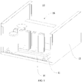
- FIG. 1 is a perspective-structural schematic view of a power module according to an embodiment of the present disclosure
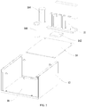
- FIG. 2 is an exploded-structural schematic view of the power module shown in the embodiment of FIG. 1 .
- the present disclosure provides a power module 10, which is usually applied in an electronic device to supply power to the electronic device.
- the power module 10 includes a power housing 12, a circuit board 14, an electronic component 16 and a first sealant layer 18.
- the circuit board 14 is connected to the power housing 12.
- a plurality of pads are arranged on a surface of the circuit board 14 facing the power housing 12.
- the electronic component 16 is arranged on the circuit board 14 and includes pins. The pins are soldered and electrically connected to the plurality of pads.
- the first sealant layer 18 is arranged on the surface of the circuit board 14 facing the power housing 12 and covers the pins and the plurality of pads.
- the plurality of pads are arranged on the surface of the circuit board 14 facing the power housing 12, such that soldering positions of the pins and the pads of the electronic component 16 are located between the circuit board 14 and the power housing 12. In this way, the electronic components 16 arranged on the circuit board 14 may not interfere with the connection between the pins and the pads.
- the first sealant layer 18 is covered at the connection positions of the pins and the pads. The layer 18 may fix the pins and the pads, such that the pins may not loosen to the pads and ensure a success connection.
- the first sealant layer 18 may also be moisture-proof, such that the pins or pads may not corrode.
- the first sealant layer 18 may also be insect-proof, such that small-sized insects may not enter the power housing 12 and the pins or pads are to be protected, thereby ensuring the success connection between the electronic component 16 and the circuit board 14. In this way, a solder stability between the pins of the electronic component 16 and the pads on the board 14 is enhanced, improving an electrical connection stability between the pins of the electronic component 16 and the pads on the circuit board 14.
- the circuit board 14 may usually be configured as a rigid circuit board to support the electronic component 16. Or, in other embodiments, the circuit board 14 may also be a flexible-hard combination board, etc., which is not specifically limited herein
- the electronic component 16 may include an integrated chip 162, a capacitor 164 and a resistor 166.
- the circuit board 14 is arranged with conductive lines (not shown).
- the integrated chip 162 is connected to the capacitor 164 and the resistor 166 through the conductive lines.
- the first sealant layer 18 covers the conductive lines.
- the conductive lines may be prepared by etching a metal layer on the circuit board 14. Specific forming methods thereof may be referred to the prior art, which is not specifically limited herein.
- the electronic component 16 such as the integrated chip 162, the capacitor 164 and the resistor 166 may be arranged on the circuit board 14.
- the pins of the electronic component 16 are electrically connected with the conductive lines to form an integrated circuit such as power-supply integrated circuit and filtering integrated circuit, which is not limited herein.
- the first sealant layer 18 is arranged to cover the conductive lines, such that the conductive lines may not be rusted and disconnected or damaged by insects due to the protective effect of the first sealant layer 18 on the conductive lines, thereby prolonging the service life of the circuit board 14.
- the first sealant layer 18 may also insulate the conductive circuit from external circuits, such that the conductive circuit may not be connected to other circuits causing short circuits.
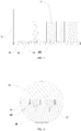
- FIG. 3 is a section-structural schematic view of the power module shown in the embodiment of FIG. 1 .
- the power module 10 further includes a heat dissipation assembly 11 in contact with the integrated chip 162 for dissipating heat for the integrated chip 162.
- the heat dissipation assembly 11 is connected to the circuit board 14, and the integrated chip 162 is sandwiched in a gap between the circuit board 14 and the heat dissipation assembly 11 to dissipate heat for the integrated chip 162.
- the temperature of the integrated chip 162 may increase due to the heat.
- the increase in the temperature of the integrated chip 162 will reduce the operating speed of the electronic device.
- the integrated chip 162 may be burned out. Therefore, in the embodiments of the present disclosure, the heat dissipation assembly 11 for dissipating heat for the integrated chip 162 is arranged on the circuit board 14 to improve the heat dissipation performance of the integrated chip 162, thereby protecting the integrated chip 162 from damages to the electronic device.
- the heat dissipation assembly 11 may include a plurality of heat dissipation fins.
- the plurality of heat dissipation fins are arranged in parallel and spaced apart to form a heat dissipation channel between adjacent heat dissipation fins, thereby increasing the heat dissipation rate of the integrated chip 162.
- the heat dissipation assembly 11 may also include a liquid-cooled radiator or a fan for heat dissipation, which is not specifically limited herein.
- the first sealant layer 18 may be a thermal conductive glue and be connected to the power housing 12 and the circuit board 14 respectively, such that a heat conduction of the power housing 12 and the circuit board 14 is achieved via the first sealant layer 18.
- an end of the first sealant layer 18 is connected to the power housing 12, and the other end of the first sealant layer 18 is connected to the circuit board 14, thereby thermally connecting the power housing 12 and the circuit board 14. Since the heat conduction efficiency of the thermal conductive glue is higher than that of air, the thermal conductive glue is sandwiched between the power housing 12 and the circuit board 14 to facilitate the transfer of heat on the circuit board 14 to the power housing 12 with a larger surface area. In this way, the power housing 12 may be configured to perform the heat dissipation for the circuit board 14, thereby improving the heat dissipation performance of the power module 10.
- the first sealant layer 18 may be arranged partially corresponding to the positions of the pads and pins.
- the first sealant layer 18 may also be evenly filled in the gap between the power housing 12 and the circuit board 14. In this way, a contact area between the thermal conductive glue and the circuit board 14 and the power housing 12 may be increased, further improving the heat dissipation performance of the power supply module 10.
- the power module 10 may further include a second sealant layer 13 covering a surface of the circuit board 14 facing away from the power housing 12.
- the second sealant layer 13 is arranged on the surface of the circuit board 14 facing away from the power housing 12.
- the second sealant layer 13 defines a vacancy at a position corresponding to the electronic component 16 to facilitate an electrical connection between the electronic component 16 and the circuit board 14.
- the first sealant layer 18 is coated on the surface of the circuit board 14 with a uniform thickness, such that dust and other debris may not fall into the gap between the electronic components 16, thereby improving a dustproof effect of the power module 10.
- FIG. 4 is a partial-enlarged schematic view of the structure shown in FIG. 3 .
- the circuit board 14 may define at least one through hole 142.
- the pins may pass through the through hole 142 and be soldered to the pads.
- the circuit board 14 defines the through hole 142 for shunning the pins.
- the length of the wiring between the pins and the pads may be reduced, thereby reducing a signal transmission loss and improving the performance of the power module 10.
- the power module 10 may further include a third sealant layer 17 sandwiched between the pins and an inner wall of the through hole 142.
- the third sealant layer 17 is sandwiched between the pins and the inner wall of the through hole 142, such that the pins may not shake relative to the circuit board 14 due to a fixing function of the third sealant layer 17 to the pins. In this way, a stability of electrical connection with the pins and pads are improved.
- the first sealant layer 18, the second sealant layer 13, and the third sealant layer 17 may be integrally formed.
- a production process of the power module 10 may be simplified to improve a production efficiency of the power module 10.
- a glue potting process may be applied.
- a molten thermally conductive glue may be poured into the inside of the power housing 12 from a glue hole. The molten thermally conductive glue will form the integrated first sealant layer 18, second sealant layer 13 and third sealant layer 17 after cooling.
- first sealant layer 18, the second sealant layer 13, and the third sealant layer 17 may also be integrally formed by other processing methods, which are not specifically limited herein.
- the first sealant layer 18 is at least one of gray glue, white glue, and epoxy resin.
- the first sealant layer 18 may be a mixture of gray glue and white glue.
- the first sealant layer 18 may include 50% gray glue and 50% white glue.
- the first sealant layer 18 may also be epoxy resin, etc., which is not specifically limited in the embodiments of the present disclosure, and may be flexibly configured according to needs.
- an electronic device in another embodiment, is also provided.
- the electronic device includes a power module.
- the structure of the power module in the embodiment is the same as the structure of the power module in the foregoing embodiments, which may be referred to the description in the foregoing embodiments and will not be repeated here.
- the electronic device may be a desktop computer host, a television, a refrigerator, a washing machine, and other electrical appliances, which are not specifically limited herein.
- the pins of the electronic component 16 and the pads may be soldered between the circuit board 14 and the power housing 12, such that the electronic component 16 arranged on the circuit board 14 may not interfere with the connection between the pins and the pads.
- the first sealant layer 18 is coveringly arranged at the connection position of the pins and the pads. The first sealant layer 18 may fix the pins and the pads, such that the pins may not loosen relative to the pads causing the connection failure.
- the first sealant layer 18 may also be moisture-proof, such that the pins or pads may not corrode.
- the first sealant layer 18 may also be insect-proof, such that small-sized insects may not enter the power housing 12 and the pins or pads are to be protected, thereby ensuring the success connection between the electronic component 16 and the circuit board 14. In this way, a solder stability between the pins of the electronic component 16 and the pads on the board 14 is enhanced, improving an electrical connection stability between the pins of the electronic component 16 and the pads on the circuit board 14.
Landscapes
- Engineering & Computer Science (AREA)
- Microelectronics & Electronic Packaging (AREA)
- Manufacturing & Machinery (AREA)
- Structures Or Materials For Encapsulating Or Coating Semiconductor Devices Or Solid State Devices (AREA)
- Non-Metallic Protective Coatings For Printed Circuits (AREA)
Abstract
Description
- The present disclosure relates to the field of electronic devices, in particular to an electronic device and a power module thereof.
- With the widespread application of electronic devices, the number of electronic components arranged on a circuit board in a power module is increasing. Pins of the electronic components are usually soldered on the circuit board. As the use time of the electronic devices is prolonged, the electrical connection between the pins of the electronic component and pads on the circuit board is likely to fail, which may cause damage to the electronic devices.
- The present disclosure provides an electronic device and a power module thereof, in order to solve the technical problems of poor stability of electrical connection of power modules in the prior art.
- In order to address the above technical problems, the present disclosure provides a power module including: a power housing; a circuit board, connected to the power housing and arranged with a plurality of pads on a surface of the circuit board facing the power housing; an electronic component, arranged on the circuit board and including a plurality of pins; wherein the plurality of pins are soldered and connected to the plurality of pads; and a first sealant layer, arranged on the surface of the circuit board facing the power housing, and covering the plurality of pins and the plurality of pads.
- In order to address the above technical problems, the present disclosure provides an electronic device, including a power module as described above.
- In the embodiments of the present disclosure, the plurality of pads are arranged on the surface of the circuit board facing the power housing, such that soldering positions of the pins and the pads of the electronic component are located between the circuit board and the power housing. In this way, the electronic components arranged on the circuit board may not interfere with the connection between the pins and the pads. The first sealant layer is covered at the connection positions of the pins and the pads. The layer may fix the pins and the pads, such that the pins may not loosen to the pads and ensure a success connection. The first sealant layer may also be moisture-proof, such that the pins or pads may not corrode. The first sealant layer may also be insect-proof, such that small-sized insects may not enter the power housing and the pins or pads are to be protected, thereby ensuring the success connection between the electronic component and the circuit board. In this way, a solder stability between the pins of the electronic component and the pads on the board is enhanced, improving an electrical connection stability between the pins of the electronic component and the pads on the circuit board.
- To further illustrate technical solutions of embodiments of the present disclosure, drawings needed for description of the embodiments will be briefly introduced. Obviously, the following drawings are only some embodiments of the present disclosure. To any one of skill in the art, other drawings may be obtained without any creative work based on the following drawings.
-
FIG. 1 is a perspective-structural schematic view of a power module according to an embodiment of the present disclosure. -
FIG. 2 is an exploded-structural schematic view of the power module shown in the embodiment ofFIG. 1 . -
FIG. 3 is a section-structural schematic view of the power module shown in the embodiment ofFIG. 1 . -
FIG. 4 is a partial-enlarged schematic view of the structure shown inFIG. 3 . - To make any one of skill in the art to understand the technical solutions of the present disclosure, the technical solutions provided by the present disclosure will be described in details by referring to the drawings and the embodiments. Obviously, the described embodiments are only a part of the embodiments, but not all the embodiments of the present disclosure. Based on the described embodiments, all other embodiments obtained by one skilled in the art without creative efforts shall fall within the scope of the present disclosure.
- Terms of "first", "second", and "third" in the present disclosure are only for descriptive purposes, and cannot be understood as indicating or implying relative importance or implicitly indicating the number of indicated technical features. Therefore, the features defined with "first", "second", and "third" may explicitly or implicitly include at least one of the features. In the description of the present disclosure, "a plurality of' means at least two, such as two, three, etc., unless otherwise specifically defined. All directional indications (such as up, down, left, right, front, back...) in the embodiments of the present disclosure are only for explaining a relative positional relationship, movement, etc. between the components in a specific posture (as shown in the drawings). When the specific posture changes, the directional indication will change accordingly. In addition, terms of "including" and "having" and any variations thereof are intended to cover non-exclusive inclusion. For example, a process, method, system, product, or device that includes a series of steps or units is not limited to the listed steps or units, but optionally includes unlisted steps or units, or optionally also includes other steps or units inherent in the process, method, product or device.
- Reference to "embodiment" herein means that a particular feature, structure, or characteristic described in connection with the embodiment may be included in at least one embodiment of the present disclosure. The appearances of this term in various places in the specification are not necessarily all referring to the same embodiment, nor are they independent or alternative embodiments that are mutually exclusive with other embodiments. It is explicitly and implicitly understood by one skilled in the art that the embodiments described herein may be combined with other embodiments.
- As shown in
FIGS. 1 and2 ,FIG. 1 is a perspective-structural schematic view of a power module according to an embodiment of the present disclosure, andFIG. 2 is an exploded-structural schematic view of the power module shown in the embodiment ofFIG. 1 . The present disclosure provides apower module 10, which is usually applied in an electronic device to supply power to the electronic device. - The
power module 10 includes apower housing 12, acircuit board 14, anelectronic component 16 and afirst sealant layer 18. Thecircuit board 14 is connected to thepower housing 12. A plurality of pads are arranged on a surface of thecircuit board 14 facing thepower housing 12. Theelectronic component 16 is arranged on thecircuit board 14 and includes pins. The pins are soldered and electrically connected to the plurality of pads. Thefirst sealant layer 18 is arranged on the surface of thecircuit board 14 facing thepower housing 12 and covers the pins and the plurality of pads. - In the embodiments of the present disclosure, the plurality of pads are arranged on the surface of the
circuit board 14 facing thepower housing 12, such that soldering positions of the pins and the pads of theelectronic component 16 are located between thecircuit board 14 and thepower housing 12. In this way, theelectronic components 16 arranged on thecircuit board 14 may not interfere with the connection between the pins and the pads. Thefirst sealant layer 18 is covered at the connection positions of the pins and the pads. Thelayer 18 may fix the pins and the pads, such that the pins may not loosen to the pads and ensure a success connection. Thefirst sealant layer 18 may also be moisture-proof, such that the pins or pads may not corrode. Thefirst sealant layer 18 may also be insect-proof, such that small-sized insects may not enter thepower housing 12 and the pins or pads are to be protected, thereby ensuring the success connection between theelectronic component 16 and thecircuit board 14. In this way, a solder stability between the pins of theelectronic component 16 and the pads on theboard 14 is enhanced, improving an electrical connection stability between the pins of theelectronic component 16 and the pads on thecircuit board 14. - In the embodiments, the
circuit board 14 may usually be configured as a rigid circuit board to support theelectronic component 16. Or, in other embodiments, thecircuit board 14 may also be a flexible-hard combination board, etc., which is not specifically limited herein - In some embodiments, as shown in
FIG. 2 , theelectronic component 16 may include an integratedchip 162, acapacitor 164 and aresistor 166. Thecircuit board 14 is arranged with conductive lines (not shown). The integratedchip 162 is connected to thecapacitor 164 and theresistor 166 through the conductive lines. Thefirst sealant layer 18 covers the conductive lines. - Specifically, the conductive lines may be prepared by etching a metal layer on the
circuit board 14. Specific forming methods thereof may be referred to the prior art, which is not specifically limited herein. Theelectronic component 16 such as the integratedchip 162, thecapacitor 164 and theresistor 166 may be arranged on thecircuit board 14. The pins of theelectronic component 16 are electrically connected with the conductive lines to form an integrated circuit such as power-supply integrated circuit and filtering integrated circuit, which is not limited herein. Thefirst sealant layer 18 is arranged to cover the conductive lines, such that the conductive lines may not be rusted and disconnected or damaged by insects due to the protective effect of thefirst sealant layer 18 on the conductive lines, thereby prolonging the service life of thecircuit board 14. In addition, thefirst sealant layer 18 may also insulate the conductive circuit from external circuits, such that the conductive circuit may not be connected to other circuits causing short circuits. - Further, as shown in
FIGS. 2 and3, FIG. 3 is a section-structural schematic view of the power module shown in the embodiment ofFIG. 1 . Thepower module 10 further includes aheat dissipation assembly 11 in contact with theintegrated chip 162 for dissipating heat for theintegrated chip 162. - Specifically, as shown in
FIGS. 2 and3 , theheat dissipation assembly 11 is connected to thecircuit board 14, and theintegrated chip 162 is sandwiched in a gap between thecircuit board 14 and theheat dissipation assembly 11 to dissipate heat for theintegrated chip 162. - Since the
integrated chip 162 generates a large amount of heat during operation, the temperature of theintegrated chip 162 may increase due to the heat. The increase in the temperature of theintegrated chip 162 will reduce the operating speed of the electronic device. When the temperature is high enough, theintegrated chip 162 may be burned out. Therefore, in the embodiments of the present disclosure, theheat dissipation assembly 11 for dissipating heat for theintegrated chip 162 is arranged on thecircuit board 14 to improve the heat dissipation performance of theintegrated chip 162, thereby protecting theintegrated chip 162 from damages to the electronic device. - The
heat dissipation assembly 11 may include a plurality of heat dissipation fins. The plurality of heat dissipation fins are arranged in parallel and spaced apart to form a heat dissipation channel between adjacent heat dissipation fins, thereby increasing the heat dissipation rate of theintegrated chip 162. - Of course, in other embodiments, the
heat dissipation assembly 11 may also include a liquid-cooled radiator or a fan for heat dissipation, which is not specifically limited herein. - Further, as shown in
FIG. 3 , thefirst sealant layer 18 may be a thermal conductive glue and be connected to thepower housing 12 and thecircuit board 14 respectively, such that a heat conduction of thepower housing 12 and thecircuit board 14 is achieved via thefirst sealant layer 18. - Specifically, an end of the
first sealant layer 18 is connected to thepower housing 12, and the other end of thefirst sealant layer 18 is connected to thecircuit board 14, thereby thermally connecting thepower housing 12 and thecircuit board 14. Since the heat conduction efficiency of the thermal conductive glue is higher than that of air, the thermal conductive glue is sandwiched between thepower housing 12 and thecircuit board 14 to facilitate the transfer of heat on thecircuit board 14 to thepower housing 12 with a larger surface area. In this way, thepower housing 12 may be configured to perform the heat dissipation for thecircuit board 14, thereby improving the heat dissipation performance of thepower module 10. - In some embodiments, the
first sealant layer 18 may be arranged partially corresponding to the positions of the pads and pins. Thefirst sealant layer 18 may also be evenly filled in the gap between thepower housing 12 and thecircuit board 14. In this way, a contact area between the thermal conductive glue and thecircuit board 14 and thepower housing 12 may be increased, further improving the heat dissipation performance of thepower supply module 10. - Furthermore, as shown in
FIG. 3 , thepower module 10 may further include asecond sealant layer 13 covering a surface of thecircuit board 14 facing away from thepower housing 12. - Specifically, the
second sealant layer 13 is arranged on the surface of thecircuit board 14 facing away from thepower housing 12. Thesecond sealant layer 13 defines a vacancy at a position corresponding to theelectronic component 16 to facilitate an electrical connection between theelectronic component 16 and thecircuit board 14. - In some embodiments, the
first sealant layer 18 is coated on the surface of thecircuit board 14 with a uniform thickness, such that dust and other debris may not fall into the gap between theelectronic components 16, thereby improving a dustproof effect of thepower module 10. - Further, as shown in
FIG. 3 and FIG. 4, FIG. 4 is a partial-enlarged schematic view of the structure shown inFIG. 3 . Thecircuit board 14 may define at least one throughhole 142. The pins may pass through the throughhole 142 and be soldered to the pads. - Specifically, the
circuit board 14 defines the throughhole 142 for shunning the pins. By defining the throughholes 142 for shunning the pins on thecircuit board 14, the length of the wiring between the pins and the pads may be reduced, thereby reducing a signal transmission loss and improving the performance of thepower module 10. - Further, the
power module 10 may further include athird sealant layer 17 sandwiched between the pins and an inner wall of the throughhole 142. Thethird sealant layer 17 is sandwiched between the pins and the inner wall of the throughhole 142, such that the pins may not shake relative to thecircuit board 14 due to a fixing function of thethird sealant layer 17 to the pins. In this way, a stability of electrical connection with the pins and pads are improved. - In the embodiments, as shown in
FIG. 4 , thefirst sealant layer 18, thesecond sealant layer 13, and thethird sealant layer 17 may be integrally formed. With the above solution, a production process of thepower module 10 may be simplified to improve a production efficiency of thepower module 10. For example, a glue potting process may be applied. A molten thermally conductive glue may be poured into the inside of thepower housing 12 from a glue hole. The molten thermally conductive glue will form the integratedfirst sealant layer 18,second sealant layer 13 andthird sealant layer 17 after cooling. - Of course, in other embodiments, the
first sealant layer 18, thesecond sealant layer 13, and thethird sealant layer 17 may also be integrally formed by other processing methods, which are not specifically limited herein. - In some embodiments, the
first sealant layer 18 is at least one of gray glue, white glue, and epoxy resin. For example, in the embodiments, thefirst sealant layer 18 may be a mixture of gray glue and white glue. Specifically, thefirst sealant layer 18 may include 50% gray glue and 50% white glue. In other embodiments, thefirst sealant layer 18 may also be epoxy resin, etc., which is not specifically limited in the embodiments of the present disclosure, and may be flexibly configured according to needs. - In another embodiment of the present disclosure, an electronic device is also provided. The electronic device includes a power module.
- The structure of the power module in the embodiment is the same as the structure of the power module in the foregoing embodiments, which may be referred to the description in the foregoing embodiments and will not be repeated here.
- In some embodiments, the electronic device may be a desktop computer host, a television, a refrigerator, a washing machine, and other electrical appliances, which are not specifically limited herein.
- In summary, those skilled in the art can easily understand that by arranging the plurality of pads on the surface of the
circuit board 14 facing thepower housing 12, the pins of theelectronic component 16 and the pads may be soldered between thecircuit board 14 and thepower housing 12, such that theelectronic component 16 arranged on thecircuit board 14 may not interfere with the connection between the pins and the pads. Thefirst sealant layer 18 is coveringly arranged at the connection position of the pins and the pads. Thefirst sealant layer 18 may fix the pins and the pads, such that the pins may not loosen relative to the pads causing the connection failure. Thefirst sealant layer 18 may also be moisture-proof, such that the pins or pads may not corrode. Thefirst sealant layer 18 may also be insect-proof, such that small-sized insects may not enter thepower housing 12 and the pins or pads are to be protected, thereby ensuring the success connection between theelectronic component 16 and thecircuit board 14. In this way, a solder stability between the pins of theelectronic component 16 and the pads on theboard 14 is enhanced, improving an electrical connection stability between the pins of theelectronic component 16 and the pads on thecircuit board 14. - The above description is for the purpose of illustrating implementations of the present disclosure, but not to limit the scope of the present disclosure. Any equivalent structural or process transformation performed based on the drawings and the specification of the present disclosure, applied directly and indirectly in other related art, should be within the scope of the present disclosure.
Claims (15)
- A power module (10), comprising:a power housing (12);a circuit board (14), connected to the power housing (12) and arranged with a plurality of pads on a surface of the circuit board (14) facing the power housing (12);an electronic component (16), arranged on the circuit board (14) and comprising a plurality of pins; wherein the plurality of pins are soldered and connected to the plurality of pads; anda first sealant layer (18), arranged on the surface of the circuit board (14) facing the power housing (12), and covering the plurality of pins and the plurality of pads.
- The power module (10) according to claim 1, wherein the first sealant layer (18) is made of a thermal conductive glue, the first sealant layer (18) is connected to the power housing (12) and the circuit board (14) respectively, such that a heat conduction of the power housing (12) and the circuit board (14) is achieved via the first sealant layer (18).
- The power module (10) according to claim 2, wherein the first sealant layer (18) is evenly filled in a gap between the power housing (12) and the circuit board (14).
- The power module according to claim 2, wherein the first sealant layer (18) is arranged partially corresponding to positions of the plurality of pins and the plurality of pads.
- The power module (10) according to claim 1, further comprising a second sealant layer (13) covering a surface of the circuit board (14) facing away from the power housing (12).
- The power module (10) according to claim 5, wherein the second sealant layer (13) defines a vacancy at a position corresponding to the electronic component (16) to facilitate an electrical connection between the electronic component (16) and the circuit board (14).
- The power module (10) according to claim 5, wherein the circuit board (14) defines a plurality of through holes (142); the plurality of pins pass through the plurality of through holes (142) and are soldered to the plurality of pads.
- The power module (10) according to claim 5, further comprising a third sealant layer (17) sandwiched between one of the plurality of pins and an inner wall of one of the plurality of through holes (142).
- The power module (10) according to claim 8, wherein the first sealant layer (18), the second sealant layer (13), and the third sealant layer (17) are integrally formed.
- The power module (10) according to claim 1, wherein the first sealant layer (18) is at least one of gray glue, white glue, and epoxy resin.
- The power module (10) according to claim 1, wherein the electronic component (16) comprises an integrated chip (162), a capacitor (164) and a resistor (166); the circuit board (14) is arranged with conductive lines; the integrated chip (162) is connected to the capacitor (164) and the resistor (166) through the conductive lines; the first sealant layer (18) covers the conductive lines.
- The power module (10) according to claim 11, further comprising a heat dissipation assembly (11) in contact with the integrated chip (162) for dissipating heat for the integrated chip (162).
- The power module (10) according to claim 12, wherein the heat dissipation assembly (11) is connected to the circuit board (14), the integrated chip (162) is sandwiched in a gap between the circuit board (14) and the heat dissipation assembly (11).
- The power module (10) according to claim 12, wherein the heat dissipation assembly (11) comprises a plurality of heat dissipation fins; the plurality of heat dissipation fins are arranged in parallel and spaced apart to form a heat dissipation channel between adjacent heat dissipation fins.
- An electronic device, comprising a power module (10) according to any one of claims 1-14.
Applications Claiming Priority (1)
| Application Number | Priority Date | Filing Date | Title |
|---|---|---|---|
| CN201922499927.5U CN211481601U (en) | 2019-12-31 | 2019-12-31 | Electronic device and power module thereof |
Publications (3)
| Publication Number | Publication Date |
|---|---|
| EP3846600A1 true EP3846600A1 (en) | 2021-07-07 |
| EP3846600B1 EP3846600B1 (en) | 2024-07-03 |
| EP3846600C0 EP3846600C0 (en) | 2024-07-03 |
Family
ID=72378094
Family Applications (1)
| Application Number | Title | Priority Date | Filing Date |
|---|---|---|---|
| EP20217469.4A Active EP3846600B1 (en) | 2019-12-31 | 2020-12-29 | Electronic device and power module thereof |
Country Status (3)
| Country | Link |
|---|---|
| US (1) | US11219137B2 (en) |
| EP (1) | EP3846600B1 (en) |
| CN (1) | CN211481601U (en) |
Citations (5)
| Publication number | Priority date | Publication date | Assignee | Title |
|---|---|---|---|---|
| DE2753145A1 (en) * | 1977-11-29 | 1979-06-07 | Bosch Gmbh Robert | ELECTRONIC CONTROL UNIT, IN PARTICULAR FOR MOUNTING ON THE ENGINE BLOCK OF MOTOR VEHICLES |
| US4833570A (en) * | 1986-12-16 | 1989-05-23 | Toyota Jidosha Kabushiki Kaisha | Electronic circuit assembly |
| US20090057006A1 (en) * | 2007-09-05 | 2009-03-05 | Kokusan Denki Co., Ltd. | Electronic unit and production method of the same |
| US20090103302A1 (en) * | 2007-10-19 | 2009-04-23 | Au Optronics Corp. | Circuit Board Assembly and Backlight Module Comprising the Same |
| DE202017006874U1 (en) * | 2017-09-20 | 2018-08-29 | Ebm-Papst St. Georgen Gmbh & Co. Kg | Circuit board assembly |
Family Cites Families (4)
| Publication number | Priority date | Publication date | Assignee | Title |
|---|---|---|---|---|
| TW200836044A (en) * | 2007-02-16 | 2008-09-01 | Delta Electronics Thailand Public Co Ltd | Heat-dissipating module |
| US7939945B2 (en) * | 2008-04-30 | 2011-05-10 | Intel Corporation | Electrically conductive fluid interconnects for integrated circuit devices |
| TWI478479B (en) * | 2013-01-17 | 2015-03-21 | 台達電子工業股份有限公司 | Integrated power module package structure |
| TWI590748B (en) * | 2013-12-19 | 2017-07-01 | 台達電子工業股份有限公司 | Heat dissipating module for casing and assembling method thereof |
-
2019
- 2019-12-31 CN CN201922499927.5U patent/CN211481601U/en active Active
-
2020
- 2020-12-23 US US17/133,587 patent/US11219137B2/en active Active
- 2020-12-29 EP EP20217469.4A patent/EP3846600B1/en active Active
Patent Citations (5)
| Publication number | Priority date | Publication date | Assignee | Title |
|---|---|---|---|---|
| DE2753145A1 (en) * | 1977-11-29 | 1979-06-07 | Bosch Gmbh Robert | ELECTRONIC CONTROL UNIT, IN PARTICULAR FOR MOUNTING ON THE ENGINE BLOCK OF MOTOR VEHICLES |
| US4833570A (en) * | 1986-12-16 | 1989-05-23 | Toyota Jidosha Kabushiki Kaisha | Electronic circuit assembly |
| US20090057006A1 (en) * | 2007-09-05 | 2009-03-05 | Kokusan Denki Co., Ltd. | Electronic unit and production method of the same |
| US20090103302A1 (en) * | 2007-10-19 | 2009-04-23 | Au Optronics Corp. | Circuit Board Assembly and Backlight Module Comprising the Same |
| DE202017006874U1 (en) * | 2017-09-20 | 2018-08-29 | Ebm-Papst St. Georgen Gmbh & Co. Kg | Circuit board assembly |
Also Published As
| Publication number | Publication date |
|---|---|
| EP3846600B1 (en) | 2024-07-03 |
| US20210204436A1 (en) | 2021-07-01 |
| EP3846600C0 (en) | 2024-07-03 |
| CN211481601U (en) | 2020-09-11 |
| US11219137B2 (en) | 2022-01-04 |
Similar Documents
| Publication | Publication Date | Title |
|---|---|---|
| EP3470899B1 (en) | Optical module packaging structure and optical module | |
| US20040196630A1 (en) | [cooling system] | |
| EP4152376B1 (en) | Chip package structure and electronic device with the same | |
| WO2021256021A1 (en) | Electronic control device | |
| US7265983B2 (en) | Power unit comprising a heat sink, and assembly method | |
| WO2014034411A1 (en) | Electric power semiconductor device | |
| US6195257B1 (en) | Apparatus and method of adapting a rectifier module to enhance cooling | |
| KR100772201B1 (en) | Thermoelectric module | |
| US11219137B2 (en) | Electronic device and power module thereof | |
| CN223414077U (en) | Power module packaging structure and electronic equipment | |
| JP2001358259A (en) | Semiconductor package | |
| CN102960079B (en) | Electronic equipment with a housing made of molded material | |
| KR200358282Y1 (en) | Terminal plate for Intelligent Power Module | |
| JP7664349B2 (en) | Package Structure | |
| JPH0322951Y2 (en) | ||
| CN209845622U (en) | Fixing device of power device needing heat dissipation insulation | |
| JPS59155158A (en) | Cooling structure of semiconductor device | |
| EP2936555B1 (en) | Chip package assembly and method to use the assembly | |
| CN219019130U (en) | High heat conduction printed circuit board | |
| JP2007299874A (en) | Thermally conductive substrate and electrically conductive substrate | |
| CN209979847U (en) | A laser transmitter, camera device and electronic device | |
| WO2018209605A1 (en) | Brushless electric tool | |
| JPH11289036A (en) | Electronic equipment | |
| JP2016039213A (en) | Substrate built-in package, semiconductor device, and module | |
| JP2019161154A (en) | Electronic circuit device |
Legal Events
| Date | Code | Title | Description |
|---|---|---|---|
| PUAI | Public reference made under article 153(3) epc to a published international application that has entered the european phase |
Free format text: ORIGINAL CODE: 0009012 |
|
| STAA | Information on the status of an ep patent application or granted ep patent |
Free format text: STATUS: THE APPLICATION HAS BEEN PUBLISHED |
|
| AK | Designated contracting states |
Kind code of ref document: A1 Designated state(s): AL AT BE BG CH CY CZ DE DK EE ES FI FR GB GR HR HU IE IS IT LI LT LU LV MC MK MT NL NO PL PT RO RS SE SI SK SM TR |
|
| STAA | Information on the status of an ep patent application or granted ep patent |
Free format text: STATUS: REQUEST FOR EXAMINATION WAS MADE |
|
| 17P | Request for examination filed |
Effective date: 20220107 |
|
| RBV | Designated contracting states (corrected) |
Designated state(s): AL AT BE BG CH CY CZ DE DK EE ES FI FR GB GR HR HU IE IS IT LI LT LU LV MC MK MT NL NO PL PT RO RS SE SI SK SM TR |
|
| GRAP | Despatch of communication of intention to grant a patent |
Free format text: ORIGINAL CODE: EPIDOSNIGR1 |
|
| STAA | Information on the status of an ep patent application or granted ep patent |
Free format text: STATUS: GRANT OF PATENT IS INTENDED |
|
| INTG | Intention to grant announced |
Effective date: 20240227 |
|
| RAP3 | Party data changed (applicant data changed or rights of an application transferred) |
Owner name: HUIZHOU FLUENCE OPTOELECTRONIC TECHNOLOGY CO., LTD. |
|
| GRAS | Grant fee paid |
Free format text: ORIGINAL CODE: EPIDOSNIGR3 |
|
| GRAA | (expected) grant |
Free format text: ORIGINAL CODE: 0009210 |
|
| STAA | Information on the status of an ep patent application or granted ep patent |
Free format text: STATUS: THE PATENT HAS BEEN GRANTED |
|
| AK | Designated contracting states |
Kind code of ref document: B1 Designated state(s): AL AT BE BG CH CY CZ DE DK EE ES FI FR GB GR HR HU IE IS IT LI LT LU LV MC MK MT NL NO PL PT RO RS SE SI SK SM TR |
|
| REG | Reference to a national code |
Ref country code: CH Ref legal event code: EP |
|
| REG | Reference to a national code |
Ref country code: DE Ref legal event code: R096 Ref document number: 602020033258 Country of ref document: DE |
|
| U01 | Request for unitary effect filed |
Effective date: 20240703 |
|
| U07 | Unitary effect registered |
Designated state(s): AT BE BG DE DK EE FI FR IT LT LU LV MT NL PT SE SI Effective date: 20240711 |
|
| U20 | Renewal fee for the european patent with unitary effect paid |
Year of fee payment: 5 Effective date: 20241127 |
|
| PG25 | Lapsed in a contracting state [announced via postgrant information from national office to epo] |
Ref country code: NO Free format text: LAPSE BECAUSE OF FAILURE TO SUBMIT A TRANSLATION OF THE DESCRIPTION OR TO PAY THE FEE WITHIN THE PRESCRIBED TIME-LIMIT Effective date: 20241003 |
|
| PG25 | Lapsed in a contracting state [announced via postgrant information from national office to epo] |
Ref country code: GR Free format text: LAPSE BECAUSE OF FAILURE TO SUBMIT A TRANSLATION OF THE DESCRIPTION OR TO PAY THE FEE WITHIN THE PRESCRIBED TIME-LIMIT Effective date: 20241004 Ref country code: PL Free format text: LAPSE BECAUSE OF FAILURE TO SUBMIT A TRANSLATION OF THE DESCRIPTION OR TO PAY THE FEE WITHIN THE PRESCRIBED TIME-LIMIT Effective date: 20240703 |
|
| PG25 | Lapsed in a contracting state [announced via postgrant information from national office to epo] |
Ref country code: IS Free format text: LAPSE BECAUSE OF FAILURE TO SUBMIT A TRANSLATION OF THE DESCRIPTION OR TO PAY THE FEE WITHIN THE PRESCRIBED TIME-LIMIT Effective date: 20241103 |
|
| PG25 | Lapsed in a contracting state [announced via postgrant information from national office to epo] |
Ref country code: HR Free format text: LAPSE BECAUSE OF FAILURE TO SUBMIT A TRANSLATION OF THE DESCRIPTION OR TO PAY THE FEE WITHIN THE PRESCRIBED TIME-LIMIT Effective date: 20240703 Ref country code: CZ Free format text: LAPSE BECAUSE OF FAILURE TO SUBMIT A TRANSLATION OF THE DESCRIPTION OR TO PAY THE FEE WITHIN THE PRESCRIBED TIME-LIMIT Effective date: 20240703 |
|
| PG25 | Lapsed in a contracting state [announced via postgrant information from national office to epo] |
Ref country code: ES Free format text: LAPSE BECAUSE OF FAILURE TO SUBMIT A TRANSLATION OF THE DESCRIPTION OR TO PAY THE FEE WITHIN THE PRESCRIBED TIME-LIMIT Effective date: 20240703 Ref country code: RS Free format text: LAPSE BECAUSE OF FAILURE TO SUBMIT A TRANSLATION OF THE DESCRIPTION OR TO PAY THE FEE WITHIN THE PRESCRIBED TIME-LIMIT Effective date: 20241003 |
|
| PG25 | Lapsed in a contracting state [announced via postgrant information from national office to epo] |
Ref country code: RS Free format text: LAPSE BECAUSE OF FAILURE TO SUBMIT A TRANSLATION OF THE DESCRIPTION OR TO PAY THE FEE WITHIN THE PRESCRIBED TIME-LIMIT Effective date: 20241003 Ref country code: PL Free format text: LAPSE BECAUSE OF FAILURE TO SUBMIT A TRANSLATION OF THE DESCRIPTION OR TO PAY THE FEE WITHIN THE PRESCRIBED TIME-LIMIT Effective date: 20240703 Ref country code: NO Free format text: LAPSE BECAUSE OF FAILURE TO SUBMIT A TRANSLATION OF THE DESCRIPTION OR TO PAY THE FEE WITHIN THE PRESCRIBED TIME-LIMIT Effective date: 20241003 Ref country code: IS Free format text: LAPSE BECAUSE OF FAILURE TO SUBMIT A TRANSLATION OF THE DESCRIPTION OR TO PAY THE FEE WITHIN THE PRESCRIBED TIME-LIMIT Effective date: 20241103 Ref country code: HR Free format text: LAPSE BECAUSE OF FAILURE TO SUBMIT A TRANSLATION OF THE DESCRIPTION OR TO PAY THE FEE WITHIN THE PRESCRIBED TIME-LIMIT Effective date: 20240703 Ref country code: GR Free format text: LAPSE BECAUSE OF FAILURE TO SUBMIT A TRANSLATION OF THE DESCRIPTION OR TO PAY THE FEE WITHIN THE PRESCRIBED TIME-LIMIT Effective date: 20241004 Ref country code: ES Free format text: LAPSE BECAUSE OF FAILURE TO SUBMIT A TRANSLATION OF THE DESCRIPTION OR TO PAY THE FEE WITHIN THE PRESCRIBED TIME-LIMIT Effective date: 20240703 Ref country code: CZ Free format text: LAPSE BECAUSE OF FAILURE TO SUBMIT A TRANSLATION OF THE DESCRIPTION OR TO PAY THE FEE WITHIN THE PRESCRIBED TIME-LIMIT Effective date: 20240703 |
|
| PG25 | Lapsed in a contracting state [announced via postgrant information from national office to epo] |
Ref country code: SM Free format text: LAPSE BECAUSE OF FAILURE TO SUBMIT A TRANSLATION OF THE DESCRIPTION OR TO PAY THE FEE WITHIN THE PRESCRIBED TIME-LIMIT Effective date: 20240703 |
|
| PG25 | Lapsed in a contracting state [announced via postgrant information from national office to epo] |
Ref country code: SK Free format text: LAPSE BECAUSE OF FAILURE TO SUBMIT A TRANSLATION OF THE DESCRIPTION OR TO PAY THE FEE WITHIN THE PRESCRIBED TIME-LIMIT Effective date: 20240703 |
|
| PLBE | No opposition filed within time limit |
Free format text: ORIGINAL CODE: 0009261 |
|
| STAA | Information on the status of an ep patent application or granted ep patent |
Free format text: STATUS: NO OPPOSITION FILED WITHIN TIME LIMIT |
|
| 26N | No opposition filed |
Effective date: 20250404 |
|
| PG25 | Lapsed in a contracting state [announced via postgrant information from national office to epo] |
Ref country code: MC Free format text: LAPSE BECAUSE OF FAILURE TO SUBMIT A TRANSLATION OF THE DESCRIPTION OR TO PAY THE FEE WITHIN THE PRESCRIBED TIME-LIMIT Effective date: 20240703 |
|
| REG | Reference to a national code |
Ref country code: CH Ref legal event code: PL |
|
| GBPC | Gb: european patent ceased through non-payment of renewal fee |
Effective date: 20241229 |
|
| PG25 | Lapsed in a contracting state [announced via postgrant information from national office to epo] |
Ref country code: GB Free format text: LAPSE BECAUSE OF NON-PAYMENT OF DUE FEES Effective date: 20241229 |
|
| PG25 | Lapsed in a contracting state [announced via postgrant information from national office to epo] |
Ref country code: CH Free format text: LAPSE BECAUSE OF NON-PAYMENT OF DUE FEES Effective date: 20241231 |
|
| PG25 | Lapsed in a contracting state [announced via postgrant information from national office to epo] |
Ref country code: IE Free format text: LAPSE BECAUSE OF NON-PAYMENT OF DUE FEES Effective date: 20241229 |
|
| PG25 | Lapsed in a contracting state [announced via postgrant information from national office to epo] |
Ref country code: RO Free format text: LAPSE BECAUSE OF FAILURE TO SUBMIT A TRANSLATION OF THE DESCRIPTION OR TO PAY THE FEE WITHIN THE PRESCRIBED TIME-LIMIT Effective date: 20240703 |
|
| U20 | Renewal fee for the european patent with unitary effect paid |
Year of fee payment: 6 Effective date: 20251127 |