EP3846210A1 - Optical package assembly and mobile terminal - Google Patents
Optical package assembly and mobile terminal Download PDFInfo
- Publication number
- EP3846210A1 EP3846210A1 EP19854240.9A EP19854240A EP3846210A1 EP 3846210 A1 EP3846210 A1 EP 3846210A1 EP 19854240 A EP19854240 A EP 19854240A EP 3846210 A1 EP3846210 A1 EP 3846210A1
- Authority
- EP
- European Patent Office
- Prior art keywords
- light
- sensor chip
- light sensor
- package assembly
- region
- Prior art date
- Legal status (The legal status is an assumption and is not a legal conclusion. Google has not performed a legal analysis and makes no representation as to the accuracy of the status listed.)
- Granted
Links
Images


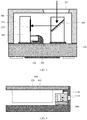
Classifications
-
- H—ELECTRICITY
- H10—SEMICONDUCTOR DEVICES; ELECTRIC SOLID-STATE DEVICES NOT OTHERWISE PROVIDED FOR
- H10F—INORGANIC SEMICONDUCTOR DEVICES SENSITIVE TO INFRARED RADIATION, LIGHT, ELECTROMAGNETIC RADIATION OF SHORTER WAVELENGTH OR CORPUSCULAR RADIATION
- H10F39/00—Integrated devices, or assemblies of multiple devices, comprising at least one element covered by group H10F30/00, e.g. radiation detectors comprising photodiode arrays
- H10F39/80—Constructional details of image sensors
- H10F39/809—Constructional details of image sensors of hybrid image sensors
-
- H—ELECTRICITY
- H04—ELECTRIC COMMUNICATION TECHNIQUE
- H04M—TELEPHONIC COMMUNICATION
- H04M1/00—Substation equipment, e.g. for use by subscribers
- H04M1/02—Constructional features of telephone sets
- H04M1/0202—Portable telephone sets, e.g. cordless phones, mobile phones or bar type handsets
- H04M1/026—Details of the structure or mounting of specific components
-
- H—ELECTRICITY
- H05—ELECTRIC TECHNIQUES NOT OTHERWISE PROVIDED FOR
- H05K—PRINTED CIRCUITS; CASINGS OR CONSTRUCTIONAL DETAILS OF ELECTRIC APPARATUS; MANUFACTURE OF ASSEMBLAGES OF ELECTRICAL COMPONENTS
- H05K5/00—Casings, cabinets or drawers for electric apparatus
- H05K5/02—Details
- H05K5/03—Covers
-
- H—ELECTRICITY
- H10—SEMICONDUCTOR DEVICES; ELECTRIC SOLID-STATE DEVICES NOT OTHERWISE PROVIDED FOR
- H10F—INORGANIC SEMICONDUCTOR DEVICES SENSITIVE TO INFRARED RADIATION, LIGHT, ELECTROMAGNETIC RADIATION OF SHORTER WAVELENGTH OR CORPUSCULAR RADIATION
- H10F39/00—Integrated devices, or assemblies of multiple devices, comprising at least one element covered by group H10F30/00, e.g. radiation detectors comprising photodiode arrays
- H10F39/80—Constructional details of image sensors
- H10F39/804—Containers or encapsulations
-
- H—ELECTRICITY
- H10—SEMICONDUCTOR DEVICES; ELECTRIC SOLID-STATE DEVICES NOT OTHERWISE PROVIDED FOR
- H10F—INORGANIC SEMICONDUCTOR DEVICES SENSITIVE TO INFRARED RADIATION, LIGHT, ELECTROMAGNETIC RADIATION OF SHORTER WAVELENGTH OR CORPUSCULAR RADIATION
- H10F39/00—Integrated devices, or assemblies of multiple devices, comprising at least one element covered by group H10F30/00, e.g. radiation detectors comprising photodiode arrays
- H10F39/80—Constructional details of image sensors
- H10F39/806—Optical elements or arrangements associated with the image sensors
- H10F39/8067—Reflectors
-
- H—ELECTRICITY
- H10—SEMICONDUCTOR DEVICES; ELECTRIC SOLID-STATE DEVICES NOT OTHERWISE PROVIDED FOR
- H10F—INORGANIC SEMICONDUCTOR DEVICES SENSITIVE TO INFRARED RADIATION, LIGHT, ELECTROMAGNETIC RADIATION OF SHORTER WAVELENGTH OR CORPUSCULAR RADIATION
- H10F77/00—Constructional details of devices covered by this subclass
- H10F77/40—Optical elements or arrangements
- H10F77/407—Optical elements or arrangements indirectly associated with the devices
-
- H—ELECTRICITY
- H10—SEMICONDUCTOR DEVICES; ELECTRIC SOLID-STATE DEVICES NOT OTHERWISE PROVIDED FOR
- H10F—INORGANIC SEMICONDUCTOR DEVICES SENSITIVE TO INFRARED RADIATION, LIGHT, ELECTROMAGNETIC RADIATION OF SHORTER WAVELENGTH OR CORPUSCULAR RADIATION
- H10F77/00—Constructional details of devices covered by this subclass
- H10F77/50—Encapsulations or containers
-
- H—ELECTRICITY
- H04—ELECTRIC COMMUNICATION TECHNIQUE
- H04M—TELEPHONIC COMMUNICATION
- H04M2250/00—Details of telephonic subscriber devices
- H04M2250/12—Details of telephonic subscriber devices including a sensor for measuring a physical value, e.g. temperature or motion
-
- H—ELECTRICITY
- H05—ELECTRIC TECHNIQUES NOT OTHERWISE PROVIDED FOR
- H05K—PRINTED CIRCUITS; CASINGS OR CONSTRUCTIONAL DETAILS OF ELECTRIC APPARATUS; MANUFACTURE OF ASSEMBLAGES OF ELECTRICAL COMPONENTS
- H05K2201/00—Indexing scheme relating to printed circuits covered by H05K1/00
- H05K2201/10—Details of components or other objects attached to or integrated in a printed circuit board
- H05K2201/10431—Details of mounted components
- H05K2201/10439—Position of a single component
- H05K2201/10454—Vertically mounted
Definitions
- the present disclosure relates to the field of mobile terminal design technologies, and in particular, to an optical package assembly and a mobile terminal.
- a mobile phone for example, a mobile phone, a wearable device, and a computer.
- performance of a current mobile terminal is optimized continuously, and a demand for light sensor chips in mobile terminals is increasing.
- the current mobile terminal develops towards a direction of large screen, space for installation of a light sensor chip in the mobile terminal is becoming more limited.
- the current mobile terminal usually uses a ribbon -shaped light sensor chip, and a width of the light sensor chip is reduced as much as possible to reduce a black border of a screen of the mobile terminal.
- the light sensor chip usually is attached to a substrate in the mobile terminal. Even if the width of the light sensor chip is reduced, the light sensor chip still occupies large space. This undoubtedly makes the black border of the screen of the mobile terminal wide and affects a further increase of a screen-to-body ratio of the mobile terminal. In addition, optical performance of the light sensor chip needs to be balanced with its size. When the size of the light sensor chip is reduced to a particular extent, a process technology hardly enables a further decrease. Obviously, it is difficult to solve, only by reducing a size of a light sensor chip, a problem that the screen-to-body ratio of the current mobile terminal can be hardly increased.
- a package assembly formed after the light sensor chip is packaged is still large and occupies a large width, eventually leading to a small screen-to-body ratio of the mobile terminal.
- the present disclosure discloses an optical package assembly, to solve a problem of a small screen-to-body ratio of a mobile terminal.
- An optical package assembly includes a substrate, a light sensor chip, and a protection portion.
- the protection portion and the light sensor chip both are fixed to the substrate, the light sensor chip is packaged in the protection portion, a plane on which the light sensor chip is located intersects with a plane of the substrate, and the protection portion includes a light entering region.
- a mobile terminal includes a display module, a housing with a frame, and the optical package assembly described above.
- the display module includes a display screen and a transparent cover plate covering the display screen, the transparent cover plate is fixed to the frame in a bonding manner, the optical package assembly is disposed in accommodation space formed by the transparent cover plate and the housing and is located between the frame and the display screen, and a light sensing region of the light sensor chip faces to the frame.
- the optical package assembly disclosed in the present disclosure changes a conventional thinking of always making a design in a direction of reducing a size of a light sensor chip.
- the light sensor chip is fixed to the substrate in such a manner that the plane on which the light sensor chip is located intersects with the plane of the substrate, and then, the light sensor chip is packaged by using the protection portion.
- a mounting manner that the light sensor chip is attached to the substrate based on the manner that the plane on which the light sensor chip is located intersects with the plane of the substrate can undoubtedly reduce a width of space occupied by the light sensor chip, thereby reducing a width of the optical package assembly to a greater extent.
- a mobile terminal equipped with the optical package assembly disclosed in the present disclosure can undoubtedly have a screen with a narrower black border, to easily increase a screen-to-body ratio of the mobile terminal.
- Substrate 200: light sensor chip; 210: light sensing region; 220: pin: 230: solder; 300: sealing compound portion; 310: light entering region; 400: sealing compound portion; 410: light entering region; 500: first reflector; 600: package cover; 610: inner cavity; 620: light entering region; 700: package cover; 710: inner cavity; 720: light entering region; 800: second reflector; 900: display module; 910: display screen; 920: transparent cover plate; 1000: housing; 1100: frame; and 1110: light entering hole.
- an embodiment of the present disclosure discloses an optical package assembly.
- the disclosed optical package assembly includes a substrate 100, a light sensor chip 200, and a protection portion.
- the substrate 100 is the basis of the entire optical package assembly.
- the light sensor chip 200 is fixed to the substrate 100 and is packaged in the protection portion.
- the protection portion plays a role of package protection.
- a plane on which the light sensor chip 200 is located intersects with a plane of the substrate 100.
- the protection portion includes a light entering region, and the light entering region can enable ambient light to enter the protection portion, so that the light sensor chip 200 senses the light.
- the light sensor chip 200 is a light sensing component, and thickness of the light sensor chip is smaller than a size in another direction.
- the protection portion and the light sensor chip 200 both are fixed to the substrate 100.
- the light sensor chip 200 intersects with the plane of the substrate 100.
- the light sensor chip 200 is attached to the plane of the substrate 100, and it may be considered that the light sensor chip 200 is parallel to the plane of the substrate 100.
- the light sensor chip 200 occupies wider space in a width direction of a frame of a mobile terminal.
- the plane on which the light sensor chip 200 is located intersects with the plane of the substrate 100. Then, it may be considered that one end of the light sensor chip 200 is high, and the other end is low, so that a width of space occupied in the width direction of the frame can be reduced.
- the optical package assembly disclosed in the embodiments of the present disclosure changes a conventional thinking of always making a design in a direction of reducing a size of the light sensor chip 200.
- the light sensor chip 200 is fixed to the substrate 100 in such a manner that the plane on which the light sensor chip 200 is located intersects with the plane of the substrate 100, and then, the light sensor chip is packaged by using the protection portion.
- a mounting manner that the light sensor chip is attached to the substrate based on the manner that the plane on which the light sensor chip 200 is located intersects with the plane of the substrate 100 can undoubtedly reduce a width of space occupied by the light sensor chip 200, thereby reducing a width of the optical package assembly to a greater extent.
- a mobile terminal equipped with the optical package assembly disclosed in the present disclosure can undoubtedly have a screen with a narrower black border, to easily increase a screen-to-body ratio of the mobile terminal.
- the plane on which the light sensor chip 200 is located is perpendicular to the plane of the substrate 100, and it may be considered that the light sensor chip 200 is located upright on the plane of the substrate 100.
- the plane on which the light sensor chip 200 is located is perpendicular to the plane of the substrate 100, so that a size of the light sensor chip 200 in the width direction of the frame of the mobile terminal is thickness of the light sensor chip 200. Because the light sensor chip 200 is thin, a width of the optical package assembly can be reduced to the greatest extent.
- the light sensor chip 200 includes a light sensing region 210, and the protection portion packages the light sensor chip 200, to play roles of packaging and protection.
- the protection portion needs to be provided with a light entering region, to ensure that ambient light can enter the light sensing region 210, to implement light sensing.
- the substrate 100 is a circuit board.
- the substrate 100 is a circuit board, the light sensor chip 200 is fixed to the substrate 100, so that the substrate 100 can supply power.
- the substrate 100 may be a specific circuit board that provides a mounting basis for the light sensor chip 200 in the mobile terminal, or may be a master board or a slave board of the mobile terminal.
- the substrate 100 is a circuit board belongings only to the optical package assembly, and after the optical package assembly is formed, the substrate 100 may be attached to the master board of the mobile terminal, to implement integral mounting of the optical package assembly.
- the light sensor chip 200 may be adhered to the substrate 100 by using glue, or may be welded to the substrate 100.
- the light sensor chip 200 generally includes a pin 220, the pin 220 may be welded to a pad of the substrate 100 by using solder 230, and the pin 220 is electrically connected to the substrate 100.
- the pin 220 is electrically connected to the substrate 100 through soldering.
- a manner of welding using the solder 230 not only can implement an electrical connection between the light sensor chip 200 and the substrate 100, but also can assist in fixing the light sensor chip 200.
- the pin 220 may have a plurality of structures.
- the pin 220 may be a bump protruding from a surface on one side of the light sensor chip 200.
- the protection portion has a plurality of structures, and may be formed in a plurality of manners provided that the light sensor chip 200 can sense ambient light after the light sensor chip is packaged.
- a first protection portion disclosed in this embodiment may be a sealing compound portion 300, and the sealing compound portion 300 is transparent glue.
- the sealing compound portion 300 includes a light entering region 310, and the light entering region 310 is disposed opposite to a light sensing region 210 of the light sensor chip 200.
- ambient light entering the protection portion from the light entering region 310 can be directly projected onto the light sensing region 210.
- the optical package assembly is mounted in a housing the mobile terminal, and the light sensing region 210 may directly face to the frame. In this case, a hole is directly formed on the frame, and there is no need to form a light entering hole on a plane on which a display screen is mounted on the mobile terminal. This undoubtedly further increases a screen-to-body ratio of the mobile terminal.
- a second protection portion disclosed in this embodiment may also be a sealing compound portion 400.
- the sealing compound portion 400 is transparent glue, and the sealing compound portion 400 includes a light entering region 410, a light entering direction of the light entering region 410 intersects with an orientation of a light sensing region 210 of the light sensor chip 200, a first reflector 500 is disposed in the sealing compound portion 400, and the first reflector 500 is used to receive ambient light that enters the light entering region 410, and reflect the ambient light to the light sensing region 210.
- This manner can enable the optical package assembly to be mounted in the housing of the mobile terminal, and adapt to light entering from a light entering hole formed on a transparent cover plate of a display module of the mobile terminal.
- the orientation of the light sensing region 210 may be perpendicular to the light entering direction of the light entering region 410.
- the sealing compound portion 400 may be completely made of transparent glue, or only the light entering region is made of transparent glue. Specifically, a shape of the light entering region may be determined based on a light entering hole on the housing of the mobile terminal.
- the sealing compound portion 300 and the sealing compound portion 400 may implement packaging through solidification of glue. After solidification, the light sensor chip 200 is surrounded by solidified glue. Therefore, the protection portion of the structure can improve packaging stability of the optical package assembly.
- a third protection portion disclosed in this embodiment of the present disclosure may be a package cover 600.
- the package cover 600 has an inner cavity 610, and the light sensor chip 200 is disposed in the inner cavity 610.
- the package cover 600 includes a light entering region 620, and the light entering region 620 is disposed opposite to a light sensing region 210.
- the optical package assembly is mounted in a housing of the mobile terminal, and the light sensing region 210 may directly face to the frame. In this case, a hole is directly formed on the frame, and there is no need to form a light entering hole on a plane on which a display screen is mounted on the mobile terminal. This undoubtedly further increases a screen-to-body ratio of the mobile terminal.
- Regions on the package cover 600 may be a non-transparent region, except for the light entering region 620, so that interference of light from the another region other than the light entering region 620 can be reduced as much as possible.
- a fourth protection portion disclosed in this embodiment of the present disclosure may be a package cover 700.
- the package cover 700 has an inner cavity 710, and the light sensor chip 200 is disposed in the inner cavity 710.
- the package cover 700 includes a light entering region 720, a light entering direction of the light entering region 720 intersects with an orientation of a light sensing region 210 of the light sensor chip 200, a second reflector 800 is disposed in the inner cavity 710, and the second reflector 800 is used to receive ambient light that enters the light entering region 410, and reflect the ambient light to the light sensing region 210.
- This manner can enable the optical package assembly to be mounted in the housing of the mobile terminal, and adapt to light entering from a light entering hole formed on a transparent cover plate of a display module of the mobile terminal.
- the light entering direction of the light entering region 720 may be perpendicular to the orientation of the light sensing region 210.
- the light sensing region 210 of the light sensor chip 200 faces to the frame of the mobile terminal, and the light entering region of the protection portion may face to the frame, to receive ambient light received from the light entering hole on the frame.
- the light entering region may alternatively face to the transparent cover plate of the mobile terminal, and receive ambient light through the light entering hole on the transparent cover plate.
- an embodiment of the present disclosure discloses a mobile terminal.
- the disclosed mobile terminal may include a display module 900, a housing 1000 with a frame 1100, and the optical package assembly described above.
- the display module 900 includes a display screen 910 and a transparent cover plate 920 covering the display screen 910, the transparent cover plate 920 is fixed to the frame 1100 in a bonding manner, the optical package assembly is disposed in accommodation space formed by the transparent cover plate 920 and the housing 1000 and is located between the frame 1100 and the display screen 910, and a light sensing region 210 faces to the frame 1100.
- the light entering hole is formed on the transparent cover plate 920.
- the light entering region faces to the transparent cover plate 920, the light entering hole is formed on the transparent cover plate 920, and the light entering hole is used to guide the ambient light to the light entering region.
- the light entering region faces to the frame 1100, the light entering hole 1110 is formed on the frame 1100, and the light entering hole 1110 is used to guide the ambient light to the light entering region.
- the light entering hole 1110 can be formed on the frame of the mobile terminal to implement light entering, and there is no need to form the light entering hole on the transparent cover plate 920. Therefore, a full screen mobile terminal with no hole on a screen can be formed.
- the mobile terminal disclosed in this embodiment of the present disclosure may be a smartphone, a tablet computer, a wearable device, or the like.
- a specific type of the mobile terminal is not limited in this embodiment of the present disclosure.
Landscapes
- Engineering & Computer Science (AREA)
- Signal Processing (AREA)
- Microelectronics & Electronic Packaging (AREA)
- Telephone Set Structure (AREA)
- Light Receiving Elements (AREA)
- Devices For Indicating Variable Information By Combining Individual Elements (AREA)
Abstract
Description
- This application claims priority to
Chinese Patent Application No. 201811010221.1 filed in China on August 30, 2018 - The present disclosure relates to the field of mobile terminal design technologies, and in particular, to an optical package assembly and a mobile terminal.
- Currently, there are various types of mobile terminals on the market, for example, a mobile phone, a wearable device, and a computer. As user demands increase, performance of a current mobile terminal is optimized continuously, and a demand for light sensor chips in mobile terminals is increasing. As the current mobile terminal develops towards a direction of large screen, space for installation of a light sensor chip in the mobile terminal is becoming more limited. Based on this, the current mobile terminal usually uses a ribbon -shaped light sensor chip, and a width of the light sensor chip is reduced as much as possible to reduce a black border of a screen of the mobile terminal.
- The light sensor chip usually is attached to a substrate in the mobile terminal. Even if the width of the light sensor chip is reduced, the light sensor chip still occupies large space. This undoubtedly makes the black border of the screen of the mobile terminal wide and affects a further increase of a screen-to-body ratio of the mobile terminal. In addition, optical performance of the light sensor chip needs to be balanced with its size. When the size of the light sensor chip is reduced to a particular extent, a process technology hardly enables a further decrease. Obviously, it is difficult to solve, only by reducing a size of a light sensor chip, a problem that the screen-to-body ratio of the current mobile terminal can be hardly increased.
- On such basis, a package assembly formed after the light sensor chip is packaged is still large and occupies a large width, eventually leading to a small screen-to-body ratio of the mobile terminal.
- The present disclosure discloses an optical package assembly, to solve a problem of a small screen-to-body ratio of a mobile terminal.
- To solve the foregoing problem, the following technical solutions are used in the present disclosure:
- An optical package assembly includes a substrate, a light sensor chip, and a protection portion. The protection portion and the light sensor chip both are fixed to the substrate, the light sensor chip is packaged in the protection portion, a plane on which the light sensor chip is located intersects with a plane of the substrate, and the protection portion includes a light entering region.
- A mobile terminal includes a display module, a housing with a frame, and the optical package assembly described above. The display module includes a display screen and a transparent cover plate covering the display screen, the transparent cover plate is fixed to the frame in a bonding manner, the optical package assembly is disposed in accommodation space formed by the transparent cover plate and the housing and is located between the frame and the display screen, and a light sensing region of the light sensor chip faces to the frame.
- The following beneficial effects can be achieved by using the technical solutions used in the present disclosure.
- The optical package assembly disclosed in the present disclosure changes a conventional thinking of always making a design in a direction of reducing a size of a light sensor chip. The light sensor chip is fixed to the substrate in such a manner that the plane on which the light sensor chip is located intersects with the plane of the substrate, and then, the light sensor chip is packaged by using the protection portion. Compared with a mounting manner that the light sensor chip is attached to the substrate, based on the manner that the plane on which the light sensor chip is located intersects with the plane of the substrate can undoubtedly reduce a width of space occupied by the light sensor chip, thereby reducing a width of the optical package assembly to a greater extent. In addition, a mobile terminal equipped with the optical package assembly disclosed in the present disclosure can undoubtedly have a screen with a narrower black border, to easily increase a screen-to-body ratio of the mobile terminal.
- The accompanying drawings illustrated herein are provided to further understand the present disclosure and form a part of the present disclosure. The exemplary embodiments of the present disclosure and the descriptions thereof are used to explain the present disclosure and do not constitute an improper limitation on the present disclosure. In the accompanying drawings:
-
FIG. 1 is a schematic structural diagram of a first optical package assembly according to an embodiment of the present disclosure; -
FIG. 2 is a schematic structural diagram of a second optical package assembly according to an embodiment of the present disclosure; -
FIG. 3 is a schematic structural diagram of a third optical package assembly according to an embodiment of the present disclosure; -
FIG. 4 is a schematic structural diagram of a fourth optical package assembly according to an embodiment of the present disclosure; and -
FIG. 5 is a schematic diagram of a partial structure of a mobile terminal according to an embodiment of the present disclosure. - 100: Substrate; 200: light sensor chip; 210: light sensing region; 220: pin: 230: solder; 300: sealing compound portion; 310: light entering region; 400: sealing compound portion; 410: light entering region; 500: first reflector; 600: package cover; 610: inner cavity; 620: light entering region; 700: package cover; 710: inner cavity; 720: light entering region; 800: second reflector; 900: display module; 910: display screen; 920: transparent cover plate; 1000: housing; 1100: frame; and 1110: light entering hole.
- To make the objectives, technical solutions, and advantages of the present disclosure clearer, the following clearly and completely describes the technical solutions in the present disclosure with reference to specific embodiments of the present disclosure and the corresponding accompanying drawings. Apparently, the described embodiments are some rather than all of the embodiments of the present disclosure. All other embodiments obtained by a person of ordinary skill in the art based on the embodiments of the present disclosure without creative efforts shall fall within the protection scope of the present disclosure.
- The technical solutions disclosed in the embodiments of the present disclosure are described in detail with reference to the accompanying drawings.
- Referring to
FIG. 1 to FIG. 5 , an embodiment of the present disclosure discloses an optical package assembly. The disclosed optical package assembly includes asubstrate 100, alight sensor chip 200, and a protection portion. - The
substrate 100 is the basis of the entire optical package assembly. Thelight sensor chip 200 is fixed to thesubstrate 100 and is packaged in the protection portion. The protection portion plays a role of package protection. A plane on which thelight sensor chip 200 is located intersects with a plane of thesubstrate 100. The protection portion includes a light entering region, and the light entering region can enable ambient light to enter the protection portion, so that thelight sensor chip 200 senses the light. - In this embodiment, the
light sensor chip 200 is a light sensing component, and thickness of the light sensor chip is smaller than a size in another direction. The protection portion and thelight sensor chip 200 both are fixed to thesubstrate 100. Thelight sensor chip 200 intersects with the plane of thesubstrate 100. In a related technology, thelight sensor chip 200 is attached to the plane of thesubstrate 100, and it may be considered that thelight sensor chip 200 is parallel to the plane of thesubstrate 100. In this case, thelight sensor chip 200 occupies wider space in a width direction of a frame of a mobile terminal. The plane on which thelight sensor chip 200 is located intersects with the plane of thesubstrate 100. Then, it may be considered that one end of thelight sensor chip 200 is high, and the other end is low, so that a width of space occupied in the width direction of the frame can be reduced. - The optical package assembly disclosed in the embodiments of the present disclosure changes a conventional thinking of always making a design in a direction of reducing a size of the
light sensor chip 200. Thelight sensor chip 200 is fixed to thesubstrate 100 in such a manner that the plane on which thelight sensor chip 200 is located intersects with the plane of thesubstrate 100, and then, the light sensor chip is packaged by using the protection portion. Compared with a mounting manner that the light sensor chip is attached to the substrate, based on the manner that the plane on which thelight sensor chip 200 is located intersects with the plane of thesubstrate 100 can undoubtedly reduce a width of space occupied by thelight sensor chip 200, thereby reducing a width of the optical package assembly to a greater extent. In addition, a mobile terminal equipped with the optical package assembly disclosed in the present disclosure can undoubtedly have a screen with a narrower black border, to easily increase a screen-to-body ratio of the mobile terminal. - In a specific implementation, the plane on which the
light sensor chip 200 is located is perpendicular to the plane of thesubstrate 100, and it may be considered that thelight sensor chip 200 is located upright on the plane of thesubstrate 100. The plane on which thelight sensor chip 200 is located is perpendicular to the plane of thesubstrate 100, so that a size of thelight sensor chip 200 in the width direction of the frame of the mobile terminal is thickness of thelight sensor chip 200. Because thelight sensor chip 200 is thin, a width of the optical package assembly can be reduced to the greatest extent. - In this embodiment, the
light sensor chip 200 includes alight sensing region 210, and the protection portion packages thelight sensor chip 200, to play roles of packaging and protection. The protection portion needs to be provided with a light entering region, to ensure that ambient light can enter thelight sensing region 210, to implement light sensing. - Optionally, the
substrate 100 is a circuit board. When thesubstrate 100 is a circuit board, thelight sensor chip 200 is fixed to thesubstrate 100, so that thesubstrate 100 can supply power. Thesubstrate 100 may be a specific circuit board that provides a mounting basis for thelight sensor chip 200 in the mobile terminal, or may be a master board or a slave board of the mobile terminal. For the convenience of assembly, in an optional solution, thesubstrate 100 is a circuit board belongings only to the optical package assembly, and after the optical package assembly is formed, thesubstrate 100 may be attached to the master board of the mobile terminal, to implement integral mounting of the optical package assembly. - The
light sensor chip 200 may be adhered to thesubstrate 100 by using glue, or may be welded to thesubstrate 100. Thelight sensor chip 200 generally includes apin 220, thepin 220 may be welded to a pad of thesubstrate 100 by usingsolder 230, and thepin 220 is electrically connected to thesubstrate 100. In a specific implementation, thepin 220 is electrically connected to thesubstrate 100 through soldering. A manner of welding using thesolder 230 not only can implement an electrical connection between thelight sensor chip 200 and thesubstrate 100, but also can assist in fixing thelight sensor chip 200. - The
pin 220 may have a plurality of structures. In a specific implementation, thepin 220 may be a bump protruding from a surface on one side of thelight sensor chip 200. - The protection portion has a plurality of structures, and may be formed in a plurality of manners provided that the
light sensor chip 200 can sense ambient light after the light sensor chip is packaged. Referring toFIG. 1 , a first protection portion disclosed in this embodiment may be a sealingcompound portion 300, and the sealingcompound portion 300 is transparent glue. The sealingcompound portion 300 includes alight entering region 310, and thelight entering region 310 is disposed opposite to alight sensing region 210 of thelight sensor chip 200. In this case, ambient light entering the protection portion from thelight entering region 310 can be directly projected onto thelight sensing region 210. In a packaging process, the optical package assembly is mounted in a housing the mobile terminal, and thelight sensing region 210 may directly face to the frame. In this case, a hole is directly formed on the frame, and there is no need to form a light entering hole on a plane on which a display screen is mounted on the mobile terminal. This undoubtedly further increases a screen-to-body ratio of the mobile terminal. - Referring to
FIG. 2 , a second protection portion disclosed in this embodiment may also be a sealingcompound portion 400. The sealingcompound portion 400 is transparent glue, and the sealingcompound portion 400 includes alight entering region 410, a light entering direction of thelight entering region 410 intersects with an orientation of alight sensing region 210 of thelight sensor chip 200, afirst reflector 500 is disposed in the sealingcompound portion 400, and thefirst reflector 500 is used to receive ambient light that enters thelight entering region 410, and reflect the ambient light to thelight sensing region 210. This manner can enable the optical package assembly to be mounted in the housing of the mobile terminal, and adapt to light entering from a light entering hole formed on a transparent cover plate of a display module of the mobile terminal. In a specific implementation, the orientation of thelight sensing region 210 may be perpendicular to the light entering direction of thelight entering region 410. - The sealing
compound portion 400 may be completely made of transparent glue, or only the light entering region is made of transparent glue. Specifically, a shape of the light entering region may be determined based on a light entering hole on the housing of the mobile terminal. - The sealing
compound portion 300 and the sealingcompound portion 400 may implement packaging through solidification of glue. After solidification, thelight sensor chip 200 is surrounded by solidified glue. Therefore, the protection portion of the structure can improve packaging stability of the optical package assembly. - Referring to
FIG. 3 , a third protection portion disclosed in this embodiment of the present disclosure may be apackage cover 600. Thepackage cover 600 has aninner cavity 610, and thelight sensor chip 200 is disposed in theinner cavity 610. Thepackage cover 600 includes alight entering region 620, and thelight entering region 620 is disposed opposite to alight sensing region 210. In a packaging process, the optical package assembly is mounted in a housing of the mobile terminal, and thelight sensing region 210 may directly face to the frame. In this case, a hole is directly formed on the frame, and there is no need to form a light entering hole on a plane on which a display screen is mounted on the mobile terminal. This undoubtedly further increases a screen-to-body ratio of the mobile terminal. - Regions on the
package cover 600 may be a non-transparent region, except for thelight entering region 620, so that interference of light from the another region other than thelight entering region 620 can be reduced as much as possible. - Referring to
FIG. 4 , a fourth protection portion disclosed in this embodiment of the present disclosure may be apackage cover 700. Thepackage cover 700 has aninner cavity 710, and thelight sensor chip 200 is disposed in theinner cavity 710. Thepackage cover 700 includes alight entering region 720, a light entering direction of thelight entering region 720 intersects with an orientation of alight sensing region 210 of thelight sensor chip 200, asecond reflector 800 is disposed in theinner cavity 710, and thesecond reflector 800 is used to receive ambient light that enters thelight entering region 410, and reflect the ambient light to thelight sensing region 210. This manner can enable the optical package assembly to be mounted in the housing of the mobile terminal, and adapt to light entering from a light entering hole formed on a transparent cover plate of a display module of the mobile terminal. In a specific implementation, the light entering direction of thelight entering region 720 may be perpendicular to the orientation of thelight sensing region 210. - As described above, when the optical package assembly is mounted in the mobile terminal, the
light sensing region 210 of thelight sensor chip 200 faces to the frame of the mobile terminal, and the light entering region of the protection portion may face to the frame, to receive ambient light received from the light entering hole on the frame. Certainly, the light entering region may alternatively face to the transparent cover plate of the mobile terminal, and receive ambient light through the light entering hole on the transparent cover plate. - Based on the optical package assembly disclosed in the embodiments of the present disclosure, an embodiment of the present disclosure discloses a mobile terminal. As shown in
FIG. 5 , the disclosed mobile terminal may include adisplay module 900, ahousing 1000 with aframe 1100, and the optical package assembly described above. Thedisplay module 900 includes adisplay screen 910 and atransparent cover plate 920 covering thedisplay screen 910, thetransparent cover plate 920 is fixed to theframe 1100 in a bonding manner, the optical package assembly is disposed in accommodation space formed by thetransparent cover plate 920 and thehousing 1000 and is located between theframe 1100 and thedisplay screen 910, and alight sensing region 210 faces to theframe 1100. - As described above, there are a plurality of manners of disposing the light entering region, and there are a plurality of relative location relationships between the light entering region and the
light sensing region 210. Correspondingly, there are a plurality of locations for forming the light entering hole on the mobile terminal. Usually, the light entering hole is formed on thetransparent cover plate 920. In a specific implementation, the light entering region faces to thetransparent cover plate 920, the light entering hole is formed on thetransparent cover plate 920, and the light entering hole is used to guide the ambient light to the light entering region. - In an optional solution, the light entering region faces to the
frame 1100, thelight entering hole 1110 is formed on theframe 1100, and thelight entering hole 1110 is used to guide the ambient light to the light entering region. Based on the structure, thelight entering hole 1110 can be formed on the frame of the mobile terminal to implement light entering, and there is no need to form the light entering hole on thetransparent cover plate 920. Therefore, a full screen mobile terminal with no hole on a screen can be formed. - The mobile terminal disclosed in this embodiment of the present disclosure may be a smartphone, a tablet computer, a wearable device, or the like. A specific type of the mobile terminal is not limited in this embodiment of the present disclosure.
- The embodiments of the present disclosure emphasize on differences between the embodiments. Different optimization features between the embodiments can be combined to form a better embodiment provided that there is no contradiction. For brief description, details are not described herein again.
- The foregoing descriptions are merely embodiments of the present disclosure, but are not intended to limit the present disclosure. A person skilled in the art may make various modifications and changes to the present disclosure. Any modification, equivalent replacement, or improvement made within the spirit and principle of the present disclosure shall fall within the protection scope of the claims of the present disclosure.
Claims (10)
- An optical package assembly, comprising: a substrate (100), a light sensor chip (200), and a protection portion, wherein the protection portion and the light sensor chip (200) both are fixed to the substrate (100), the light sensor chip (200) is packaged in the protection portion, a plane on which the light sensor chip (200) is located intersects with a plane of the substrate (100), and the protection portion comprises a light entering region.
- The optical package assembly according to claim 1, wherein the plane on which the light sensor chip (200) is located is perpendicular to the plane of the substrate (100).
- The optical package assembly according to claim 1, wherein the substrate (100) is a circuit board, the light sensor chip (200) comprises a pin (220), the pin (220) is welded to a pad of the substrate (100) by using solder (230), and the pin (220) is electrically connected to the substrate (100).
- The optical package assembly according to claim 3, wherein the pin (220) is a bump protruding from a surface on one side of the light sensor chip (200).
- The optical package assembly according to claim 1, wherein the protection portion is a sealing compound portion (300), the sealing compound portion (300) is transparent glue, the sealing compound portion (300) comprises the light entering region (310), and the light entering region (310) is disposed opposite to a light sensing region (210) of the light sensor chip (200).
- The optical package assembly according to claim 1, wherein the protection portion is a sealing compound portion (400), the sealing compound portion (400) is transparent glue, the sealing compound portion (400) comprises the light entering region (410), a light entering direction of the light entering region(410) intersects with an orientation of a light sensing region (210) of the light sensor chip (200), a first reflector (500) is disposed in the sealing compound portion (400), and the first reflector (500) is used to receive ambient light that enters the light entering region (410), and reflect the ambient light to the light sensing region (210).
- The optical package assembly according to claim 1, wherein the protection portion is a package cover (600), the package cover (600) has an inner cavity (610), the light sensor chip (200) is disposed in the inner cavity (610), the package cover (600) comprises the light entering region (620), and the light entering region (620) is disposed opposite to a light sensing region (210) of the light sensor chip (200).
- The optical package assembly according to claim 1, wherein the protection portion is a package cover (700), the package cover (700) has an inner cavity (710), the light sensor chip (200) is disposed in the inner cavity (710), the package cover (700) comprises the light entering region (720), a light entering direction of the light entering region (720) intersects with an orientation of a light sensing region (210) of the light sensor chip (200), a second reflector (800) is disposed in the inner cavity (710), and the second reflector (800) is used to receive ambient light that enters the light entering region (410), and reflect the ambient light to the light sensing region (210).
- A mobile terminal, comprising: a display module (900), a housing (1000) with a frame (1100), and the optical package assembly according to any one of claims 1 to 8, wherein the display module (900) comprises a display screen (910) and a transparent cover plate (920) covering the display screen (910), the transparent cover plate (920) is fixed to the frame (1100) in a bonding manner, the optical package assembly is disposed in accommodation space formed by the transparent cover plate (920) and the housing (1000) and is located between the frame (1100) and the display screen (910), and a light sensing region (210) of the light sensor chip (200) faces to the frame (1100).
- The mobile terminal according to claim 9, wherein the mobile terminal is a smartphone, a tablet computer, or a wearable device.
Applications Claiming Priority (2)
| Application Number | Priority Date | Filing Date | Title |
|---|---|---|---|
| CN201811010221.1A CN109244093B (en) | 2018-08-30 | 2018-08-30 | An optical package component and a mobile terminal |
| PCT/CN2019/096698 WO2020042824A1 (en) | 2018-08-30 | 2019-07-19 | Optical package assembly and mobile terminal |
Publications (3)
| Publication Number | Publication Date |
|---|---|
| EP3846210A1 true EP3846210A1 (en) | 2021-07-07 |
| EP3846210A4 EP3846210A4 (en) | 2021-11-10 |
| EP3846210B1 EP3846210B1 (en) | 2024-04-17 |
Family
ID=65069285
Family Applications (1)
| Application Number | Title | Priority Date | Filing Date |
|---|---|---|---|
| EP19854240.9A Active EP3846210B1 (en) | 2018-08-30 | 2019-07-19 | Optical package assembly and mobile terminal |
Country Status (5)
| Country | Link |
|---|---|
| US (1) | US11552201B2 (en) |
| EP (1) | EP3846210B1 (en) |
| CN (1) | CN109244093B (en) |
| ES (1) | ES2982327T3 (en) |
| WO (1) | WO2020042824A1 (en) |
Families Citing this family (2)
| Publication number | Priority date | Publication date | Assignee | Title |
|---|---|---|---|---|
| CN109244093B (en) * | 2018-08-30 | 2020-09-29 | 维沃移动通信有限公司 | An optical package component and a mobile terminal |
| TWI876560B (en) * | 2023-05-12 | 2025-03-11 | 光寶科技股份有限公司 | Light emitting device |
Family Cites Families (17)
| Publication number | Priority date | Publication date | Assignee | Title |
|---|---|---|---|---|
| KR101594367B1 (en) * | 2009-09-02 | 2016-02-26 | 엘지전자 주식회사 | A mobile terminal |
| CN106125153B (en) | 2012-06-11 | 2019-06-04 | 原相科技股份有限公司 | Package structure of optical device |
| US9664555B2 (en) * | 2012-12-18 | 2017-05-30 | Apple Inc. | Electronic devices with light sensors |
| US10555436B1 (en) * | 2014-09-02 | 2020-02-04 | Apple Inc. | Electronic device with thermal management system |
| CN106302878B (en) * | 2016-08-17 | 2019-11-19 | 青岛海信移动通信技术股份有限公司 | a mobile terminal |
| US10591645B2 (en) * | 2016-09-19 | 2020-03-17 | Apple Inc. | Electronic devices having scratch-resistant antireflection coatings |
| DE102016122810A1 (en) * | 2016-11-25 | 2018-05-30 | Osram Opto Semiconductors Gmbh | COMPONENT WITH A LIGHT-EMITTING SEMICONDUCTOR CHIP |
| CN107367803A (en) | 2017-08-28 | 2017-11-21 | 华进半导体封装先导技术研发中心有限公司 | A kind of light module package structure and preparation method |
| US10914901B2 (en) * | 2017-10-17 | 2021-02-09 | International Business Machines Corporation | Lateral mounting of optoelectronic chips on organic substrate |
| CN108111643B (en) * | 2017-11-30 | 2021-01-22 | Oppo广东移动通信有限公司 | Mobile terminal |
| CN107945683B (en) * | 2018-01-08 | 2020-11-03 | 陆少韬 | Front end assembly applied to intelligent equipment |
| CN108418909A (en) * | 2018-01-30 | 2018-08-17 | 努比亚技术有限公司 | A kind of photosensitive adjusting part for mobile terminal |
| CN108040155B (en) * | 2018-02-07 | 2021-01-08 | 维沃移动通信有限公司 | A kind of photosensitive component and mobile terminal |
| CN108462767A (en) * | 2018-02-07 | 2018-08-28 | 维沃移动通信有限公司 | A kind of photosensitive components and mobile terminal |
| US10847478B2 (en) * | 2018-02-27 | 2020-11-24 | Amkor Technology Singapore Holding Pte. Ltd. | Method of forming an electronic device structure having an electronic component with an on-edge orientation and related structures |
| CN108415514B (en) * | 2018-04-27 | 2021-04-20 | 宇龙计算机通信科技(深圳)有限公司 | an electronic device |
| CN109244093B (en) * | 2018-08-30 | 2020-09-29 | 维沃移动通信有限公司 | An optical package component and a mobile terminal |
-
2018
- 2018-08-30 CN CN201811010221.1A patent/CN109244093B/en active Active
-
2019
- 2019-07-19 WO PCT/CN2019/096698 patent/WO2020042824A1/en not_active Ceased
- 2019-07-19 EP EP19854240.9A patent/EP3846210B1/en active Active
- 2019-07-19 ES ES19854240T patent/ES2982327T3/en active Active
-
2021
- 2021-02-23 US US17/182,881 patent/US11552201B2/en active Active
Also Published As
| Publication number | Publication date |
|---|---|
| WO2020042824A1 (en) | 2020-03-05 |
| CN109244093B (en) | 2020-09-29 |
| CN109244093A (en) | 2019-01-18 |
| EP3846210B1 (en) | 2024-04-17 |
| EP3846210A4 (en) | 2021-11-10 |
| ES2982327T3 (en) | 2024-10-15 |
| US11552201B2 (en) | 2023-01-10 |
| US20210217902A1 (en) | 2021-07-15 |
Similar Documents
| Publication | Publication Date | Title |
|---|---|---|
| US10831298B2 (en) | Touch display module, display device and transparent optical adhesive layer structure | |
| WO2022037374A1 (en) | Electronic device | |
| US11552201B2 (en) | Optical package assembly and mobile terminal | |
| WO2021185237A1 (en) | Circuit board assembly and electronic device | |
| US10763413B2 (en) | Light emitting diode with pads on side surface thereof, light emitting device and display device including the light emitting diode | |
| CN112835238B (en) | Electronic device and housing assembly | |
| CN216119308U (en) | Screen assembly and mobile terminal | |
| CN211457101U (en) | Quartz resonator base with external thermistor | |
| US20220291570A1 (en) | Base, camera module and electronic device | |
| CN110636701A (en) | Circuit board assembly and electronic equipment | |
| US20220294941A1 (en) | Base, camera module and electronic device | |
| CN110198404B (en) | Camera module, electronic equipment and camera module manufacturing method | |
| US12614851B2 (en) | Display module and electronic device | |
| CN108600446A (en) | Mobile terminal | |
| CN210137339U (en) | Electronic equipment | |
| CN115022502B (en) | Camera module and electronic equipment | |
| CN219981037U (en) | MEMS microphones and electronic equipment | |
| CN213403167U (en) | Circuit board assemblies, camera modules, electronic equipment and in-vehicle equipment | |
| JP6743219B2 (en) | Imaging module and portable electronic device | |
| CN221886934U (en) | Mobile terminal based on low-cost sealing structure | |
| CN222795168U (en) | Electronic equipment and sensor module | |
| CN223427204U (en) | Display module and terminal equipment | |
| CN218849492U (en) | Miniature LED display module assembly and electronic equipment | |
| CN216291124U (en) | Camera module and electronic equipment | |
| EP4421588A1 (en) | Electronic device with a stepped battery |
Legal Events
| Date | Code | Title | Description |
|---|---|---|---|
| STAA | Information on the status of an ep patent application or granted ep patent |
Free format text: STATUS: THE INTERNATIONAL PUBLICATION HAS BEEN MADE |
|
| STAA | Information on the status of an ep patent application or granted ep patent |
Free format text: STATUS: REQUEST FOR EXAMINATION WAS MADE |
|
| PUAI | Public reference made under article 153(3) epc to a published international application that has entered the european phase |
Free format text: ORIGINAL CODE: 0009012 |
|
| 17P | Request for examination filed |
Effective date: 20210330 |
|
| AK | Designated contracting states |
Kind code of ref document: A1 Designated state(s): AL AT BE BG CH CY CZ DE DK EE ES FI FR GB GR HR HU IE IS IT LI LT LU LV MC MK MT NL NO PL PT RO RS SE SI SK SM TR |
|
| A4 | Supplementary search report drawn up and despatched |
Effective date: 20211011 |
|
| RIC1 | Information provided on ipc code assigned before grant |
Ipc: H04M 1/02 20060101ALI20211005BHEP Ipc: H01L 27/146 20060101AFI20211005BHEP |
|
| DAV | Request for validation of the european patent (deleted) | ||
| DAX | Request for extension of the european patent (deleted) | ||
| STAA | Information on the status of an ep patent application or granted ep patent |
Free format text: STATUS: EXAMINATION IS IN PROGRESS |
|
| 17Q | First examination report despatched |
Effective date: 20230208 |
|
| GRAP | Despatch of communication of intention to grant a patent |
Free format text: ORIGINAL CODE: EPIDOSNIGR1 |
|
| STAA | Information on the status of an ep patent application or granted ep patent |
Free format text: STATUS: GRANT OF PATENT IS INTENDED |
|
| INTG | Intention to grant announced |
Effective date: 20240117 |
|
| GRAS | Grant fee paid |
Free format text: ORIGINAL CODE: EPIDOSNIGR3 |
|
| GRAA | (expected) grant |
Free format text: ORIGINAL CODE: 0009210 |
|
| STAA | Information on the status of an ep patent application or granted ep patent |
Free format text: STATUS: THE PATENT HAS BEEN GRANTED |
|
| AK | Designated contracting states |
Kind code of ref document: B1 Designated state(s): AL AT BE BG CH CY CZ DE DK EE ES FI FR GB GR HR HU IE IS IT LI LT LU LV MC MK MT NL NO PL PT RO RS SE SI SK SM TR |
|
| REG | Reference to a national code |
Ref country code: GB Ref legal event code: FG4D |
|
| REG | Reference to a national code |
Ref country code: CH Ref legal event code: EP |
|
| REG | Reference to a national code |
Ref country code: DE Ref legal event code: R096 Ref document number: 602019050608 Country of ref document: DE |
|
| REG | Reference to a national code |
Ref country code: IE Ref legal event code: FG4D |
|
| REG | Reference to a national code |
Ref country code: NL Ref legal event code: FP |
|
| REG | Reference to a national code |
Ref country code: LT Ref legal event code: MG9D |
|
| REG | Reference to a national code |
Ref country code: AT Ref legal event code: MK05 Ref document number: 1678119 Country of ref document: AT Kind code of ref document: T Effective date: 20240417 |
|
| PG25 | Lapsed in a contracting state [announced via postgrant information from national office to epo] |
Ref country code: IS Free format text: LAPSE BECAUSE OF FAILURE TO SUBMIT A TRANSLATION OF THE DESCRIPTION OR TO PAY THE FEE WITHIN THE PRESCRIBED TIME-LIMIT Effective date: 20240817 |
|
| PG25 | Lapsed in a contracting state [announced via postgrant information from national office to epo] |
Ref country code: BG Free format text: LAPSE BECAUSE OF FAILURE TO SUBMIT A TRANSLATION OF THE DESCRIPTION OR TO PAY THE FEE WITHIN THE PRESCRIBED TIME-LIMIT Effective date: 20240417 |
|
| PG25 | Lapsed in a contracting state [announced via postgrant information from national office to epo] |
Ref country code: HR Free format text: LAPSE BECAUSE OF FAILURE TO SUBMIT A TRANSLATION OF THE DESCRIPTION OR TO PAY THE FEE WITHIN THE PRESCRIBED TIME-LIMIT Effective date: 20240417 Ref country code: FI Free format text: LAPSE BECAUSE OF FAILURE TO SUBMIT A TRANSLATION OF THE DESCRIPTION OR TO PAY THE FEE WITHIN THE PRESCRIBED TIME-LIMIT Effective date: 20240417 |
|
| PG25 | Lapsed in a contracting state [announced via postgrant information from national office to epo] |
Ref country code: GR Free format text: LAPSE BECAUSE OF FAILURE TO SUBMIT A TRANSLATION OF THE DESCRIPTION OR TO PAY THE FEE WITHIN THE PRESCRIBED TIME-LIMIT Effective date: 20240718 |
|
| PG25 | Lapsed in a contracting state [announced via postgrant information from national office to epo] |
Ref country code: PT Free format text: LAPSE BECAUSE OF FAILURE TO SUBMIT A TRANSLATION OF THE DESCRIPTION OR TO PAY THE FEE WITHIN THE PRESCRIBED TIME-LIMIT Effective date: 20240819 |
|
| REG | Reference to a national code |
Ref country code: ES Ref legal event code: FG2A Ref document number: 2982327 Country of ref document: ES Kind code of ref document: T3 Effective date: 20241015 |
|
| PG25 | Lapsed in a contracting state [announced via postgrant information from national office to epo] |
Ref country code: AT Free format text: LAPSE BECAUSE OF FAILURE TO SUBMIT A TRANSLATION OF THE DESCRIPTION OR TO PAY THE FEE WITHIN THE PRESCRIBED TIME-LIMIT Effective date: 20240417 |
|
| PG25 | Lapsed in a contracting state [announced via postgrant information from national office to epo] |
Ref country code: PL Free format text: LAPSE BECAUSE OF FAILURE TO SUBMIT A TRANSLATION OF THE DESCRIPTION OR TO PAY THE FEE WITHIN THE PRESCRIBED TIME-LIMIT Effective date: 20240417 |
|
| PG25 | Lapsed in a contracting state [announced via postgrant information from national office to epo] |
Ref country code: LV Free format text: LAPSE BECAUSE OF FAILURE TO SUBMIT A TRANSLATION OF THE DESCRIPTION OR TO PAY THE FEE WITHIN THE PRESCRIBED TIME-LIMIT Effective date: 20240417 |
|
| PG25 | Lapsed in a contracting state [announced via postgrant information from national office to epo] |
Ref country code: PT Free format text: LAPSE BECAUSE OF FAILURE TO SUBMIT A TRANSLATION OF THE DESCRIPTION OR TO PAY THE FEE WITHIN THE PRESCRIBED TIME-LIMIT Effective date: 20240819 Ref country code: PL Free format text: LAPSE BECAUSE OF FAILURE TO SUBMIT A TRANSLATION OF THE DESCRIPTION OR TO PAY THE FEE WITHIN THE PRESCRIBED TIME-LIMIT Effective date: 20240417 Ref country code: NO Free format text: LAPSE BECAUSE OF FAILURE TO SUBMIT A TRANSLATION OF THE DESCRIPTION OR TO PAY THE FEE WITHIN THE PRESCRIBED TIME-LIMIT Effective date: 20240717 Ref country code: LV Free format text: LAPSE BECAUSE OF FAILURE TO SUBMIT A TRANSLATION OF THE DESCRIPTION OR TO PAY THE FEE WITHIN THE PRESCRIBED TIME-LIMIT Effective date: 20240417 Ref country code: IS Free format text: LAPSE BECAUSE OF FAILURE TO SUBMIT A TRANSLATION OF THE DESCRIPTION OR TO PAY THE FEE WITHIN THE PRESCRIBED TIME-LIMIT Effective date: 20240817 Ref country code: HR Free format text: LAPSE BECAUSE OF FAILURE TO SUBMIT A TRANSLATION OF THE DESCRIPTION OR TO PAY THE FEE WITHIN THE PRESCRIBED TIME-LIMIT Effective date: 20240417 Ref country code: GR Free format text: LAPSE BECAUSE OF FAILURE TO SUBMIT A TRANSLATION OF THE DESCRIPTION OR TO PAY THE FEE WITHIN THE PRESCRIBED TIME-LIMIT Effective date: 20240718 Ref country code: FI Free format text: LAPSE BECAUSE OF FAILURE TO SUBMIT A TRANSLATION OF THE DESCRIPTION OR TO PAY THE FEE WITHIN THE PRESCRIBED TIME-LIMIT Effective date: 20240417 Ref country code: BG Free format text: LAPSE BECAUSE OF FAILURE TO SUBMIT A TRANSLATION OF THE DESCRIPTION OR TO PAY THE FEE WITHIN THE PRESCRIBED TIME-LIMIT Effective date: 20240417 Ref country code: AT Free format text: LAPSE BECAUSE OF FAILURE TO SUBMIT A TRANSLATION OF THE DESCRIPTION OR TO PAY THE FEE WITHIN THE PRESCRIBED TIME-LIMIT Effective date: 20240417 Ref country code: RS Free format text: LAPSE BECAUSE OF FAILURE TO SUBMIT A TRANSLATION OF THE DESCRIPTION OR TO PAY THE FEE WITHIN THE PRESCRIBED TIME-LIMIT Effective date: 20240717 |
|
| REG | Reference to a national code |
Ref country code: DE Ref legal event code: R079 Ref document number: 602019050608 Country of ref document: DE Free format text: PREVIOUS MAIN CLASS: H01L0027146000 Ipc: H10F0039180000 |
|
| PG25 | Lapsed in a contracting state [announced via postgrant information from national office to epo] |
Ref country code: DK Free format text: LAPSE BECAUSE OF FAILURE TO SUBMIT A TRANSLATION OF THE DESCRIPTION OR TO PAY THE FEE WITHIN THE PRESCRIBED TIME-LIMIT Effective date: 20240417 |
|
| REG | Reference to a national code |
Ref country code: DE Ref legal event code: R097 Ref document number: 602019050608 Country of ref document: DE |
|
| PG25 | Lapsed in a contracting state [announced via postgrant information from national office to epo] |
Ref country code: EE Free format text: LAPSE BECAUSE OF FAILURE TO SUBMIT A TRANSLATION OF THE DESCRIPTION OR TO PAY THE FEE WITHIN THE PRESCRIBED TIME-LIMIT Effective date: 20240417 |
|
| PG25 | Lapsed in a contracting state [announced via postgrant information from national office to epo] |
Ref country code: CZ Free format text: LAPSE BECAUSE OF FAILURE TO SUBMIT A TRANSLATION OF THE DESCRIPTION OR TO PAY THE FEE WITHIN THE PRESCRIBED TIME-LIMIT Effective date: 20240417 |
|
| PG25 | Lapsed in a contracting state [announced via postgrant information from national office to epo] |
Ref country code: SK Free format text: LAPSE BECAUSE OF FAILURE TO SUBMIT A TRANSLATION OF THE DESCRIPTION OR TO PAY THE FEE WITHIN THE PRESCRIBED TIME-LIMIT Effective date: 20240417 Ref country code: RO Free format text: LAPSE BECAUSE OF FAILURE TO SUBMIT A TRANSLATION OF THE DESCRIPTION OR TO PAY THE FEE WITHIN THE PRESCRIBED TIME-LIMIT Effective date: 20240417 |
|
| PG25 | Lapsed in a contracting state [announced via postgrant information from national office to epo] |
Ref country code: SM Free format text: LAPSE BECAUSE OF FAILURE TO SUBMIT A TRANSLATION OF THE DESCRIPTION OR TO PAY THE FEE WITHIN THE PRESCRIBED TIME-LIMIT Effective date: 20240417 |
|
| PG25 | Lapsed in a contracting state [announced via postgrant information from national office to epo] |
Ref country code: SM Free format text: LAPSE BECAUSE OF FAILURE TO SUBMIT A TRANSLATION OF THE DESCRIPTION OR TO PAY THE FEE WITHIN THE PRESCRIBED TIME-LIMIT Effective date: 20240417 Ref country code: SK Free format text: LAPSE BECAUSE OF FAILURE TO SUBMIT A TRANSLATION OF THE DESCRIPTION OR TO PAY THE FEE WITHIN THE PRESCRIBED TIME-LIMIT Effective date: 20240417 Ref country code: RO Free format text: LAPSE BECAUSE OF FAILURE TO SUBMIT A TRANSLATION OF THE DESCRIPTION OR TO PAY THE FEE WITHIN THE PRESCRIBED TIME-LIMIT Effective date: 20240417 Ref country code: EE Free format text: LAPSE BECAUSE OF FAILURE TO SUBMIT A TRANSLATION OF THE DESCRIPTION OR TO PAY THE FEE WITHIN THE PRESCRIBED TIME-LIMIT Effective date: 20240417 Ref country code: DK Free format text: LAPSE BECAUSE OF FAILURE TO SUBMIT A TRANSLATION OF THE DESCRIPTION OR TO PAY THE FEE WITHIN THE PRESCRIBED TIME-LIMIT Effective date: 20240417 Ref country code: CZ Free format text: LAPSE BECAUSE OF FAILURE TO SUBMIT A TRANSLATION OF THE DESCRIPTION OR TO PAY THE FEE WITHIN THE PRESCRIBED TIME-LIMIT Effective date: 20240417 |
|
| PG25 | Lapsed in a contracting state [announced via postgrant information from national office to epo] |
Ref country code: MC Free format text: LAPSE BECAUSE OF FAILURE TO SUBMIT A TRANSLATION OF THE DESCRIPTION OR TO PAY THE FEE WITHIN THE PRESCRIBED TIME-LIMIT Effective date: 20240417 |
|
| PLBE | No opposition filed within time limit |
Free format text: ORIGINAL CODE: 0009261 |
|
| STAA | Information on the status of an ep patent application or granted ep patent |
Free format text: STATUS: NO OPPOSITION FILED WITHIN TIME LIMIT |
|
| REG | Reference to a national code |
Ref country code: CH Ref legal event code: PL |
|
| PG25 | Lapsed in a contracting state [announced via postgrant information from national office to epo] |
Ref country code: LU Free format text: LAPSE BECAUSE OF NON-PAYMENT OF DUE FEES Effective date: 20240719 |
|
| 26N | No opposition filed |
Effective date: 20250120 |
|
| PG25 | Lapsed in a contracting state [announced via postgrant information from national office to epo] |
Ref country code: LU Free format text: LAPSE BECAUSE OF NON-PAYMENT OF DUE FEES Effective date: 20240719 |
|
| PG25 | Lapsed in a contracting state [announced via postgrant information from national office to epo] |
Ref country code: SI Free format text: LAPSE BECAUSE OF FAILURE TO SUBMIT A TRANSLATION OF THE DESCRIPTION OR TO PAY THE FEE WITHIN THE PRESCRIBED TIME-LIMIT Effective date: 20240417 Ref country code: CH Free format text: LAPSE BECAUSE OF NON-PAYMENT OF DUE FEES Effective date: 20240731 Ref country code: BE Free format text: LAPSE BECAUSE OF NON-PAYMENT OF DUE FEES Effective date: 20240731 |
|
| REG | Reference to a national code |
Ref country code: BE Ref legal event code: MM Effective date: 20240731 |
|
| PGFP | Annual fee paid to national office [announced via postgrant information from national office to epo] |
Ref country code: GB Payment date: 20250529 Year of fee payment: 7 |
|
| PGFP | Annual fee paid to national office [announced via postgrant information from national office to epo] |
Ref country code: NL Payment date: 20250613 Year of fee payment: 7 |
|
| PGFP | Annual fee paid to national office [announced via postgrant information from national office to epo] |
Ref country code: FR Payment date: 20250610 Year of fee payment: 7 |
|
| PG25 | Lapsed in a contracting state [announced via postgrant information from national office to epo] |
Ref country code: IE Free format text: LAPSE BECAUSE OF NON-PAYMENT OF DUE FEES Effective date: 20240719 |
|
| PG25 | Lapsed in a contracting state [announced via postgrant information from national office to epo] |
Ref country code: SE Free format text: LAPSE BECAUSE OF FAILURE TO SUBMIT A TRANSLATION OF THE DESCRIPTION OR TO PAY THE FEE WITHIN THE PRESCRIBED TIME-LIMIT Effective date: 20240417 |
|
| PGFP | Annual fee paid to national office [announced via postgrant information from national office to epo] |
Ref country code: ES Payment date: 20250805 Year of fee payment: 7 |
|
| PGFP | Annual fee paid to national office [announced via postgrant information from national office to epo] |
Ref country code: DE Payment date: 20250528 Year of fee payment: 7 |
|
| PGFP | Annual fee paid to national office [announced via postgrant information from national office to epo] |
Ref country code: IT Payment date: 20250623 Year of fee payment: 7 |
|
| PG25 | Lapsed in a contracting state [announced via postgrant information from national office to epo] |
Ref country code: CY Free format text: LAPSE BECAUSE OF FAILURE TO SUBMIT A TRANSLATION OF THE DESCRIPTION OR TO PAY THE FEE WITHIN THE PRESCRIBED TIME-LIMIT; INVALID AB INITIO Effective date: 20190719 |
|
| PG25 | Lapsed in a contracting state [announced via postgrant information from national office to epo] |
Ref country code: HU Free format text: LAPSE BECAUSE OF FAILURE TO SUBMIT A TRANSLATION OF THE DESCRIPTION OR TO PAY THE FEE WITHIN THE PRESCRIBED TIME-LIMIT; INVALID AB INITIO Effective date: 20190719 |