EP3843009A1 - Rfid tag substrate, rfid tag, and rfid system - Google Patents
Rfid tag substrate, rfid tag, and rfid system Download PDFInfo
- Publication number
- EP3843009A1 EP3843009A1 EP19851820.1A EP19851820A EP3843009A1 EP 3843009 A1 EP3843009 A1 EP 3843009A1 EP 19851820 A EP19851820 A EP 19851820A EP 3843009 A1 EP3843009 A1 EP 3843009A1
- Authority
- EP
- European Patent Office
- Prior art keywords
- conductor
- electrode
- capacitance
- rfid tag
- distance
- Prior art date
- Legal status (The legal status is an assumption and is not a legal conclusion. Google has not performed a legal analysis and makes no representation as to the accuracy of the status listed.)
- Granted
Links
Images





Classifications
-
- H—ELECTRICITY
- H01—ELECTRIC ELEMENTS
- H01Q—ANTENNAS, i.e. RADIO AERIALS
- H01Q9/00—Electrically-short antennas having dimensions not more than twice the operating wavelength and consisting of conductive active radiating elements
- H01Q9/04—Resonant antennas
- H01Q9/0407—Substantially flat resonant element parallel to ground plane, e.g. patch antenna
- H01Q9/0421—Substantially flat resonant element parallel to ground plane, e.g. patch antenna with a shorting wall or a shorting pin at one end of the element
-
- G—PHYSICS
- G06—COMPUTING OR CALCULATING; COUNTING
- G06K—GRAPHICAL DATA READING; PRESENTATION OF DATA; RECORD CARRIERS; HANDLING RECORD CARRIERS
- G06K19/00—Record carriers for use with machines and with at least a part designed to carry digital markings
- G06K19/06—Record carriers for use with machines and with at least a part designed to carry digital markings characterised by the kind of the digital marking, e.g. shape, nature, code
- G06K19/067—Record carriers with conductive marks, printed circuits or semiconductor circuit elements, e.g. credit or identity cards also with resonating or responding marks without active components
- G06K19/07—Record carriers with conductive marks, printed circuits or semiconductor circuit elements, e.g. credit or identity cards also with resonating or responding marks without active components with integrated circuit chips
- G06K19/077—Constructional details, e.g. mounting of circuits in the carrier
- G06K19/07745—Mounting details of integrated circuit chips
-
- G—PHYSICS
- G06—COMPUTING OR CALCULATING; COUNTING
- G06K—GRAPHICAL DATA READING; PRESENTATION OF DATA; RECORD CARRIERS; HANDLING RECORD CARRIERS
- G06K19/00—Record carriers for use with machines and with at least a part designed to carry digital markings
- G06K19/06—Record carriers for use with machines and with at least a part designed to carry digital markings characterised by the kind of the digital marking, e.g. shape, nature, code
- G06K19/067—Record carriers with conductive marks, printed circuits or semiconductor circuit elements, e.g. credit or identity cards also with resonating or responding marks without active components
- G06K19/07—Record carriers with conductive marks, printed circuits or semiconductor circuit elements, e.g. credit or identity cards also with resonating or responding marks without active components with integrated circuit chips
- G06K19/077—Constructional details, e.g. mounting of circuits in the carrier
- G06K19/07745—Mounting details of integrated circuit chips
- G06K19/07747—Mounting details of integrated circuit chips at least one of the integrated circuit chips being mounted as a module
-
- G—PHYSICS
- G06—COMPUTING OR CALCULATING; COUNTING
- G06K—GRAPHICAL DATA READING; PRESENTATION OF DATA; RECORD CARRIERS; HANDLING RECORD CARRIERS
- G06K19/00—Record carriers for use with machines and with at least a part designed to carry digital markings
- G06K19/06—Record carriers for use with machines and with at least a part designed to carry digital markings characterised by the kind of the digital marking, e.g. shape, nature, code
- G06K19/067—Record carriers with conductive marks, printed circuits or semiconductor circuit elements, e.g. credit or identity cards also with resonating or responding marks without active components
- G06K19/07—Record carriers with conductive marks, printed circuits or semiconductor circuit elements, e.g. credit or identity cards also with resonating or responding marks without active components with integrated circuit chips
- G06K19/077—Constructional details, e.g. mounting of circuits in the carrier
- G06K19/07749—Constructional details, e.g. mounting of circuits in the carrier the record carrier being capable of non-contact communication, e.g. constructional details of the antenna of a non-contact smart card
- G06K19/07758—Constructional details, e.g. mounting of circuits in the carrier the record carrier being capable of non-contact communication, e.g. constructional details of the antenna of a non-contact smart card arrangements for adhering the record carrier to further objects or living beings, functioning as an identification tag
-
- G—PHYSICS
- G06—COMPUTING OR CALCULATING; COUNTING
- G06K—GRAPHICAL DATA READING; PRESENTATION OF DATA; RECORD CARRIERS; HANDLING RECORD CARRIERS
- G06K19/00—Record carriers for use with machines and with at least a part designed to carry digital markings
- G06K19/06—Record carriers for use with machines and with at least a part designed to carry digital markings characterised by the kind of the digital marking, e.g. shape, nature, code
- G06K19/067—Record carriers with conductive marks, printed circuits or semiconductor circuit elements, e.g. credit or identity cards also with resonating or responding marks without active components
- G06K19/07—Record carriers with conductive marks, printed circuits or semiconductor circuit elements, e.g. credit or identity cards also with resonating or responding marks without active components with integrated circuit chips
- G06K19/077—Constructional details, e.g. mounting of circuits in the carrier
- G06K19/07749—Constructional details, e.g. mounting of circuits in the carrier the record carrier being capable of non-contact communication, e.g. constructional details of the antenna of a non-contact smart card
- G06K19/07773—Antenna details
-
- G—PHYSICS
- G06—COMPUTING OR CALCULATING; COUNTING
- G06K—GRAPHICAL DATA READING; PRESENTATION OF DATA; RECORD CARRIERS; HANDLING RECORD CARRIERS
- G06K19/00—Record carriers for use with machines and with at least a part designed to carry digital markings
- G06K19/06—Record carriers for use with machines and with at least a part designed to carry digital markings characterised by the kind of the digital marking, e.g. shape, nature, code
- G06K19/067—Record carriers with conductive marks, printed circuits or semiconductor circuit elements, e.g. credit or identity cards also with resonating or responding marks without active components
- G06K19/07—Record carriers with conductive marks, printed circuits or semiconductor circuit elements, e.g. credit or identity cards also with resonating or responding marks without active components with integrated circuit chips
- G06K19/077—Constructional details, e.g. mounting of circuits in the carrier
- G06K19/07749—Constructional details, e.g. mounting of circuits in the carrier the record carrier being capable of non-contact communication, e.g. constructional details of the antenna of a non-contact smart card
- G06K19/07773—Antenna details
- G06K19/07786—Antenna details the antenna being of the HF type, such as a dipole
-
- G—PHYSICS
- G06—COMPUTING OR CALCULATING; COUNTING
- G06K—GRAPHICAL DATA READING; PRESENTATION OF DATA; RECORD CARRIERS; HANDLING RECORD CARRIERS
- G06K19/00—Record carriers for use with machines and with at least a part designed to carry digital markings
- G06K19/06—Record carriers for use with machines and with at least a part designed to carry digital markings characterised by the kind of the digital marking, e.g. shape, nature, code
- G06K19/067—Record carriers with conductive marks, printed circuits or semiconductor circuit elements, e.g. credit or identity cards also with resonating or responding marks without active components
- G06K19/07—Record carriers with conductive marks, printed circuits or semiconductor circuit elements, e.g. credit or identity cards also with resonating or responding marks without active components with integrated circuit chips
- G06K19/077—Constructional details, e.g. mounting of circuits in the carrier
- G06K19/07749—Constructional details, e.g. mounting of circuits in the carrier the record carrier being capable of non-contact communication, e.g. constructional details of the antenna of a non-contact smart card
- G06K19/07773—Antenna details
- G06K19/0779—Antenna details the antenna being foldable or folded
-
- H—ELECTRICITY
- H01—ELECTRIC ELEMENTS
- H01Q—ANTENNAS, i.e. RADIO AERIALS
- H01Q1/00—Details of, or arrangements associated with, antennas
- H01Q1/12—Supports; Mounting means
- H01Q1/22—Supports; Mounting means by structural association with other equipment or articles
- H01Q1/2208—Supports; Mounting means by structural association with other equipment or articles associated with components used in interrogation type services, i.e. in systems for information exchange between an interrogator/reader and a tag/transponder, e.g. in Radio Frequency Identification [RFID] systems
- H01Q1/2225—Supports; Mounting means by structural association with other equipment or articles associated with components used in interrogation type services, i.e. in systems for information exchange between an interrogator/reader and a tag/transponder, e.g. in Radio Frequency Identification [RFID] systems used in active tags, i.e. provided with its own power source or in passive tags, i.e. deriving power from RF signal
-
- H—ELECTRICITY
- H01—ELECTRIC ELEMENTS
- H01Q—ANTENNAS, i.e. RADIO AERIALS
- H01Q9/00—Electrically-short antennas having dimensions not more than twice the operating wavelength and consisting of conductive active radiating elements
- H01Q9/04—Resonant antennas
- H01Q9/0407—Substantially flat resonant element parallel to ground plane, e.g. patch antenna
- H01Q9/0414—Substantially flat resonant element parallel to ground plane, e.g. patch antenna in a stacked or folded configuration
Definitions
- the present disclosure relates to an RFID (Radio Frequency Identifier) tag board, an RFID tag and an RFID system.
- RFID Radio Frequency Identifier
- an RFID system is used conventionally that transmits and receives information with an RFID tag(s) to and from an article(s) by wireless communication.
- an RFID tag having an RFID tag board provided with an antenna, such as a plate-like inverted-F antenna, and a semiconductor integrated circuit mounted on a plate surface of the RFID tag board is widely used (e.g. WO 2013/145312 A1 ).
- the RFID tag can transmit radio waves containing information stored in the semiconductor integrated circuit and also write information contained in received radio waves into the semiconductor integrated circuit.
- an RFID system using such an RFID tag(s) for example, an RFID tag is attached to an article, and a predetermined reader/writer obtains information on the article from the RFID tag or writes necessary information into the RFID tag.
- articles can be managed.
- An RFID tag board of an aspect of the present disclosure has a plate surface on which a semiconductor integrated circuit is to be mounted, is used with the plate surface and the semiconductor integrated circuit thereon sealed with a sealing member, and includes:
- An RFID tag of an aspect of the present disclosure includes:
- An RFID system of an aspect of the present disclosure includes:
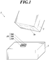
- FIG. 1 shows an RFID system 1 according to a first embodiment of the present disclosure.
- the RFID system 1 includes an RFID tag 10 and a reader/writer 2 that transmits and receives radio waves to and from the RFID tag 10.
- the RFID tag 10 is used, for example, by being attached to the surface of an article 3 to manage.
- the RFID tag 10 is a type having no built-in battery, and receives electric power from the reader/writer 2 via electromagnetic waves and operates by this electric power.
- the RFID tag 10 may be a type having a built-in battery.
- the RFID tag 10 includes an RFID tag board 100, an RFID tag IC (Integrated Circuit) 200 (semiconductor integrated circuit) mounted on a plate surface of the RFID tag board 100, and a sealing member 300 for sealing the plate surface, on which the RFID tag IC 200 is mounted, of the RFID tag board 100 and the RFID tag IC 200.
- RFID tag IC Integrated Circuit
- the RFID tag board 100 is a rectangular-parallelepiped-shaped plate-like member in which a plate-like inverted-F antenna is formed. The configuration thereof will be described later in detail.
- the RFID tag IC 200 includes a controller that performs control about transmission and reception of radio waves, a storage that stores, for example, information on the article 3, and a feeding terminal 201 (shown in FIG. 3 ) and a reference potential terminal 202 (shown in FIG. 3 ) that are electrically connected to the antenna of the RFID tag board 100. Under the control of the controller, the RFID tag IC 200 obtains instruction information contained in radio waves received by the antenna and performs a process corresponding to the instruction information (e.g. rewrites information stored in the storage), and also causes the antenna to transmit (radiate) radio waves containing information specified by the instruction information.
- a controller that performs control about transmission and reception of radio waves
- a storage that stores, for example, information on the article 3
- a feeding terminal 201 shown in FIG. 3
- a reference potential terminal 202 shown in FIG. 3
- the sealing member 300 covers and protects the RFID tag IC 200.
- the sealing member 300 is molded such that a structural body composed of the RFID tag board 100 and the sealing member 300 becomes a rectangular parallelepiped as a whole.
- the sealing member 300 for example, epoxy resin, polyimide resin, silicone resin or the like is usable.
- Filler particles such as silica particles or glass particles, may be added to any of these resin materials. The filler particles are added thereto in order to adjust various characteristics, such as mechanical strength, moisture resistance and electrical characteristics, of the sealing member 300, for example.
- the reader/writer 2 has an antenna 2a for transmitting and receiving radio waves to and from the RFID tag 10.
- the reader/writer 2 transmits, to the RFID tag 10, radio waves containing instruction information instructing the RFID tag 10 to rewrite information or transmit information.
- the reader/writer 2 receives radio waves transmitted from the RFID tag 10 in accordance with the instruction information, obtains information contained in the radio waves, and performs a predetermined process by using the information (e.g. a process of writing the information into a predetermined storage device or a process of displaying the information on a predetermined display device).
- FIG. 2A and FIG. 2B are each a diagram for explaining the radiation state of radio waves due to the structure of an RFID tag 10.
- RFID tags there are a cavity-type RFID tag 10C as shown in FIG. 2A and a plate-type RFID tag 10 as shown in FIG. 1 or FIG. 2B .
- the plate-type RFID tag 10 is used.
- FIG. 2A and FIG. 2B a Cartesian coordinate system x, y, z defined fixedly to the RFID tag 10C and the RFID tag 10 is shown.
- the z direction may be referred to as a height direction of the RFID tag 10C and the RFID tag 10.
- the height is merely a designation for the sake of convenience, and hence the height direction herein does not always coincide with the actual height direction (vertical direction) of the RFID tag 10C and the RFID tag 10 when used.
- a recess (cavity) is provided in the upper surface of the RFID tag board 100, the RFID tag IC 200 is mounted on the bottom surface of the recess, and the inside of the recess is sealed with the sealing member 300.
- the entire upper surface of the plate-like RFID tag board 100 is sealed with the plate-like sealing member 300.
- the plate-type RFID tag 10 can be manufactured at lower cost than the cavity-type RFID tag 10C because it does not require a step of forming a recess in the RFID tag board 100, and also can be manufactured efficiently, for example, by a method of forming the sealing member 300 on the entire surface of a compound substrate containing a large number of RFID tag boards 100 and then dividing it.
- radio waves that are transmitted from the RFID tag board 100 radiate from a side surface (one of the surfaces parallel to the yz plane) of the RFID tag board 100 and travel so as to go around in the +z direction.
- a radio-wave transmittable distance from the mounting surface, on which the RFID tag 10/10C is mounted, of the article 3 in the +z direction depends on the magnitude of electric power received from the reader/writer 2, the size of the RFID tag 10/10C and so forth, but is usually within a range of about several tens of centimeters to several meters.
- Radio waves have a property of passing through a substance having a higher permittivity (relative permittivity or relative dielectric constant).
- a substance having a higher permittivity relative permittivity or relative dielectric constant.
- radio waves radiated from the side surface of the RFID tag board 100 to the outer space are likely to enter, in part, the sealing member 300, and radiate less in a desired direction (+z direction).
- the cavity-type RFID tag 10C shown in FIG. 2A because the sealing member 300 is embedded in the recess, radio waves are unlikely to enter the sealing member 300, and hardly cause the above problem.
- a radio-wave reaching distance L2 from the plate-type RFID tag 10 in the +z direction tends be shorter than a radio-wave reaching distance L1 from the cavity-type RFID tag 10C in the +z direction. That is, the plate-type RFID tag 10 is likely to have a shorter communication distance than the cavity-type RFID tag 10C has.
- the configuration of the RFID tag board 100 is optimized to make the communication distance longer.
- the configuration of the RFID tag 10 of this embodiment will be described with the focus on the structure of the RFID tag board 100.
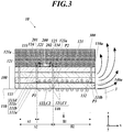
- FIG. 3 is a sectional view showing the configuration of the RFID tag 10 of this embodiment.
- FIG. 4 is an exploded perspective view of the RFID tag 10 shown in FIG. 3 .
- the RFID tag board 100 includes: an insulating substrate 110; an upper surface conductor 121 (first surface conductor), a first electrode 124 and a second electrode 125 disposed on one surface of the insulating substrate 110 (surface facing to the +z direction, which hereinafter may be referred to as an upper surface 110a); a lower surface conductor 122 (second surface conductor) disposed on the opposite surface of the insulating substrate 110 (surface facing to the -z direction, which hereinafter may be referred to as a lower surface 110b) to the one surface; a capacitance conductor 123 disposed in the insulating substrate 110 and facing part of the lower surface conductor 122 to form a capacitance element 140 (capacitor) together with the lower surface conductor 122; a short-circuit part through conductor 131 passing through the insulating substrate 110 in the thickness direction and electrically connecting the upper surface conductor 121 and the lower surface conductor 122; a capacitance part through conductor
- the RFID tag board 100 is attached and fixed to the article 3 such that the lower surface 110b (lower surface conductor 122) of the insulating substrate 110 faces the article 3.
- the RFID tag 10 of this embodiment operates even when the surface of the article 3 is formed of a conductor, such as metal. That is, when the RFID tag board 100 is attached to such an article 3, the conductive portion of the article 3 also functions as a ground conductor of the antenna of the RFID tag 10.
- the RFID tag IC 200 is mounted on the upper surface of the insulating substrate 110.
- the upper surface of the insulating substrate 110 and the RFID tag IC 200 thereon are covered and sealed with the sealing member 300. That is, the upper surface of the insulating substrate 110 constitutes the above-described plate surface, on which the RFID tag IC 200 is mounted and which is sealed with the sealing member 300, of the RFID tag board 100.
- the insulating substrate 110 is a plate-like member having a structure in which two or more (four in this embodiment) stacking substrates 111a to 111d formed of a dielectric (ceramic in this embodiment) are stacked in this order from the bottom.
- the insulating substrate 110 has the upper surface 110a and the lower surface 110b that are parallel to the xy plane, and is a rectangular parallelepiped the height (length in the z direction) of which is shorter than the width dimension (length in the x direction) and the depth dimension (length in the y direction), and the width dimension of which is longer than the depth dimension, thereby being long in the x direction.
- the stacking substrates 111a to 111d constituting the insulating substrate 110 may be formed of, for example, a dielectric, such as an aluminum oxide sintered body, an aluminum nitride sintered body, a mullite sintered body or a glass-ceramic sintered body.
- the insulating substrate 110 may be formed by stacking two or more (four in this embodiment) sheet-shaped layers (four layers in this embodiment) of ceramic green sheets on top of one another and then firing/sintering these.
- the first electrode 124 and the second electrode 125 that are rectangular when viewed in the +z direction are disposed.
- the shape of the first electrode 124 and the second electrode 125 is not limited to a rectangle, and may be another polygon, a circle or the like.
- the first electrode 124 is electrically connected via a bonding wire to, among terminals that the RFID tag IC 200 has, the feeding terminal 201 from which a voltage signal(s) relating to transmission radio waves is output.
- the first electrode 124 is disposed on the -x direction side as compared with the second electrode 125.
- the second electrode 125 is electrically connected via a bonding wire to, among the terminals that the RFID tag IC 200 has, the reference potential terminal 202 that serves as a reference potential.
- the reference potential of this embodiment is a ground potential
- the reference potential terminal 202 is a ground terminal.
- the reference potential is not limited to the ground potential, and a predetermined potential other than the ground potential may be used as the reference potential.
- the method of connecting the first electrode 124 and the second electrode 125 to the above-described terminals of the RFID tag IC 200 is not limited to the method using bonding wires, and they may be connected, for example, by flip chip mounting.
- the upper surface conductor 121 is disposed on the upper surface 110a of the insulating substrate 110.
- the upper surface conductor 121 is a plate-like conductor that is long in the x direction, and is disposed on almost the entire upper surface 110a of the insulating substrate 110 except a region where the first electrode 124 and the second electrode 125 are formed. That is, the upper surface conductor 121 has a shape having an opening 121a for ensuring the region where the first electrode 124 and the second electrode 125 are formed.
- the lower surface conductor 122 is a plate-like conductor that is long in the x direction, and is disposed on almost the entire lower surface 110b of the insulating substrate 110.
- the capacitance conductor 123 is a plate-like conductor disposed between the lowermost stacking substrate 111a and the second lowermost stacking substrate 111b of the insulating substrate 110, and faces part of the lower surface conductor 122 to form the capacitance element 140. That is, when a pair of conductors forming the capacitance element 140 is a first conductor C1 and a second conductor C2, the first conductor C1 on the +z direction side is constituted by the capacitance conductor 123, and the second conductor C2 on the -z direction side is constituted by the lower surface conductor 122.
- the capacitance conductor 123 has a circular opening 123a for allowing the interlayer through conductor 134 to pass through.
- the opening 123a is formed with a size that ensures a clearance of a predetermined distance from the interlayer through conductor 134.
- the upper surface conductor 121, the lower surface conductor 122, the capacitance conductor 123, the first electrode 124 and the second electrode 125 can be formed by, at a stage where the stacking substrates 111a to 111d are ceramic green sheets, printing metal paste at their positions on the ceramic green sheets by screen printing or another method, and firing these together. More specifically, first, metal paste for the lower surface conductor 122 is printed on the lower surface of a ceramic green sheet for the stacking substrate 111a, and metal paste for the capacitance conductor 123 is printed on the lower surface of a ceramic green sheet for the stacking substrate 111b.
- metal paste for the capacitance conductor 123 may be printed on the upper surface of a ceramic green sheet for the stacking substrate 111a, and metal paste for the lower surface conductor 122 may be printed on the lower surface thereof.
- metal paste for the upper surface conductor 121, the first electrode 124 and the second electrode 125 is printed on the upper surface of a ceramic green sheet for the stacking substrate 111d.
- the four ceramic green sheets for the stacking substrates 111a to 111d are stacked and then fired as a whole.
- the upper surface conductor 121, the lower surface conductor 122, the capacitance conductor 123, the first electrode 124 and the second electrode 125 can be formed on/in the insulating substrate 110.
- the metal paste for example, a mixed material of copper powder with an organic solvent and an organic binder is usable.
- the exposed surfaces of the upper surface conductor 121, the lower surface conductor 122, the first electrode 124 and the second electrode 125 may be coated with plating layers formed of, for example, nickel, cobalt, palladium or gold. This can inhibit oxidation corrosion.
- the first electrode 124 and the second electrode 125 coated with a plating layer(s) also improve their joining characteristics with the bonding wires.
- the short-circuit part through conductor 131 passes through layers between the upper surface 110a and the lower surface 110b of the insulating substrate 110 in the z direction to electrically connect the upper surface conductor 121 and the lower surface conductor 122.
- the short-circuit part through conductor 131 is disposed at the end part on the -x direction side in the longer direction (x direction) of the insulating substrate 110. Hence, the short-circuit part through conductor 131 is connected to the end parts on the -x direction side in the longer direction (x direction) of the upper surface conductor 121 and the lower surface conductor 122.
- An end part in the longer direction of the insulating substrate 110 is, for example, a region having a length of 10% or less of the length of the insulating substrate 110 in the longer direction from an end in the longer direction.
- the short-circuit part through conductor 131 has widths in the x direction and the y direction narrower than each of the upper surface conductor 121 and the lower surface conductor 122 has, and is pin-shaped in this embodiment.
- the capacitance part through conductor 132 is disposed in layers of the insulating substrate 110 between the upper surface conductor 121 and the capacitance conductor 123 (i.e. passes through the stacking substrates 111b to 111d in the z direction) to electrically connect the upper surface conductor 121 and the capacitance conductor 123.
- the capacitance part through conductor 132 is disposed at the end part on the +x direction side in the longer direction of the insulating substrate 110. Hence, the capacitance part through conductor 132 is connected to the end parts on the +x direction side in the longer direction of the upper surface conductor 121 and the capacitance conductor 123.
- the capacitance part through conductor 132 has widths in the x direction and the y direction narrower than each of the upper surface conductor 121 and the lower surface conductor 122 has, and is pin-shaped in this embodiment.
- one short-circuit part through conductor 131 and one capacitance part through conductor 132 are provided.
- a plurality of short-circuit part through conductors 131 may be disposed at the end part on the -x direction side of the insulating substrate 110, and a plurality of short-circuit part through conductors 131 may be disposed at the end part on the +x direction side of the insulating substrate 110.
- a plurality of conductors may be provided for only one of the short-circuit part through conductor 131 and the capacitance part through conductor 132.
- the interlayer through conductor 133 is disposed in layers of the insulating substrate 110 between the first electrode 124 and the capacitance conductor 123 (i.e. passes through the stacking substrate 111b to 111d in the z direction) to electrically connect the first electrode 124 and the capacitance conductor 123.
- the interlayer through conductor 133 is disposed so as to be superposed on the first electrode 124 when viewed in the z direction.
- the interlayer through conductor 134 passes through layers between the upper surface 110a and the lower surface 110b of the insulating substrate 110 in the z direction to electrically connect the second electrode 125 and the lower surface conductor 122.
- the interlayer through conductor 134 is disposed so as to be superposed on the second electrode 125 when viewed in the z direction. Also, the interlayer through conductor 134 is disposed so as to pass through the opening 123a of the capacitance conductor 123.
- the interlayer through conductors 133, 134 each have widths in the x direction and the y direction narrower than each of the upper surface conductor 121 and the lower surface conductor 122 has, and are pin-shaped in this embodiment.
- the short-circuit part through conductor 131, the capacitance part through conductor 132 and the interlayer through conductors 133, 134 can be formed by, at a stage where the stacking substrates 111a to 111d are ceramic green sheets, the stage being before metal paste is printed to form the upper surface conductor 121 and so forth, providing through holes or interlayer holes in the ceramic green sheets, filling the holes with the metal paste, and firing these together.
- the metal paste as with the material for the upper surface conductor 121, for example, a mixed material of copper powder with an organic solvent and an organic binder is usable.
- the upper surface conductor 121, the lower surface conductor 122, the capacitance conductor 123, the short-circuit part through conductor 131, the capacitance part through conductor 132 and the interlayer through conductors 133, 134 constitute the plate-like inverted-F antenna.
- a chain of conductors constituted by the upper surface conductor 121, the capacitance conductor 123 and the capacitance part through conductor 132 acts as a radiation conductor of the plate-like inverted-F antenna
- the lower surface conductor 122 acts as a ground conductor (which may be referred to as a ground plane or a reference potential conductor) of the plate-like inverted-F antenna.
- the short-circuit part through conductor 131 acts as an electrical wall of the plate-like inverted-F antenna
- the interlayer through conductor 133 acts as a feeder of the plate-like inverted-F antenna
- the interlayer through conductor 134 acts as a ground of the plate-like inverted-F antenna.
- radio waves mainly radiate from an open end part 140a on the +x direction side of the pair of the conductors of the capacitance element 140. After radiating to the +x direction side, the radio waves travel so as to go around to the +z direction side.
- a plate-like inverted-F antenna electrically corresponds to a patch antenna having a shape in which a radiation conductor and a short-circuit conductor on the +x direction side of an electrical wall extend to the other side (-x direction side) of the electrical wall, with the electrical wall as an axis of symmetry. That is, according to the configuration of a plate-like inverted-F antenna in which a radiation conductor and a short-circuit conductor are connected by an electrical wall, the area thereof can be reduced by half the area of a patch antenna having the same function.
- the plate-like inverted-F antenna of this embodiment has a wavelength shortening effect by part (capacitance conductor 123) of the radiation conductor and part of the short-circuit conductor (lower surface conductor 122) forming the capacitance element 140. This also contributes to miniaturization.
- connection point P1 is a point where the capacitance conductor 123 and the interlayer through conductor 133 are connected (electrical connection point on the capacitance conductor 123 with the first electrode 124).
- the interlayer through conductor 133 extends from the first electrode 124 in the - z direction, and hence in the x direction and the y direction, the connection point P1 is the same as the position of the first electrode 124.
- connection point P2 is a point where the lower surface conductor 122 and the interlayer through conductor 134 are connected (electrical connection point on the lower surface conductor 122 with the second electrode 125).
- the interlayer through conductor 134 extends from the second electrode 125 in the -z direction, and hence in the x direction and the y direction, the connection point P2 is the same as the position of the second electrode 125.
- the first electrode 124 is disposed on the -x direction side as compared with the second electrode 125.
- the connection point P1 is located on the -x direction side as compared with the connection point P2.
- a distance A1 between the first electrode 124 and the short-circuit part through conductor 131 is shorter than a distance A2 between the second electrode 125 and the short-circuit part through conductor 131.
- the distance A1 between the connection point P1 and the short-circuit part through conductor 131 is shorter than the distance A2 between the connection point P2 and the short-circuit part through conductor 131.
- a distance B1 between the first electrode 124 and the capacitance part through conductor 132 is longer than a distance B2 between the second electrode 125 and the capacitance part through conductor 132.
- the distance B1 between the connection point P1 and the capacitance part through conductor 132 is longer than the distance B2 between the connection point P2 and the capacitance part through conductor 132.
- connection point P1 is closer to the short-circuit part through conductor 131 than the connection point P2 is. This can ensure a longer section R. Advantages of this configuration will be described in comparison with the configuration of an RFID tag board 100r of a comparative example.
- FIG. 6 is a sectional view showing the configuration of the RFID tag board 100r of the comparative example.
- the positional relationship in the x direction between the first electrode 124 and the second electrode 125 is reversed from that in the RFID tag board 100 shown in FIG. 3 .
- the positional relationship in the x direction between the interlayer through conductor 133 (feeder) and the interlayer through conductor 134 (ground) is also reversed from that in the RFID tag board 100 shown in FIG. 3 .
- the distance A1 between the connection point P1 and the short-circuit part through conductor 131 is longer than the distance A2 between the connection point P2 and the short-circuit part through conductor 131.
- the distance B1 between the connection point P1 and the capacitance part through conductor 132 is shorter than the distance B2 between the connection point P2 and the capacitance part through conductor 132.
- the section R from the connection point P1 to the connection point P3, in which current flows during operation of the antennas is shorter than the section R in the RFID tag board 100 shown in FIG. 3 .
- charges accumulate less on the capacitance element 140.
- the section R, in which charges accumulate, of the capacitance element 140 is longer than the section R in the RFID tag board 100r of the comparative example shown in FIG. 6 .
- more charges accumulate on the capacitance element 140, and the potential difference generated between the conductors, which are a pair of conductors, of the capacitance element 140 can be larger.
- stronger radio waves are emitted from the plate-like inverted-F antenna, and hence a radio wave transmission distance, namely, the communication distance, can be longer.
- the RFID tag board 100 has a plate surface on which the RFID tag ID 200 is to be mounted, is used with the plate surface and the RFID tag ID 200 thereon sealed with the sealing member 300, and includes: the insulating substrate 100 one surface of which forms the plate surface; the upper surface conductor 121 that is disposed on the one surface of the insulating substrate 110; the lower surface conductor 122 that is disposed on the surface of the insulating substrate 110 opposite to the one surface; the short-circuit part through conductor 131 that passes through the insulating substrate 110 in the thickness direction to electrically connect the upper surface conductor 121 and the lower surface conductor 122; the capacitance conductor 123 that is disposed in the insulating substrate 110 and faces at least part of the lower surface conductor 122 to form the capacitance element 140; the capacitance part through conductor 132 that is disposed in the insulating substrate 110 to electrically connect the capacitance conductor 123 and the upper surface conductor 121; the first electrode 124 that is disposed on the one surface
- connection point P1 where the first electrode 124 and the capacitance conductor 123 (radiation conductor) are connected can be easily provided closer to the short-circuit part through conductor 131 than the connection point P2 where the second electrode 125 and the lower surface conductor 122 (ground conductor) are connected is. That is, by a simple configuration in which the interlayer through conductors 133, 134 extending in the thickness direction of the insulating substrate 110 connect conductors, the distance A1 from the connection point P1 to the short-circuit part through conductor 131 can be made shorter than the distance A2 from the connection point P2 to the short-circuit part through conductor 131.
- connection point P1 and the connection point P2 having this positional relationship, the section R, in which charges accumulate, of the capacitance element 140 can be made long. More specifically, by making the connection point P1, which is the end part position on the short-circuit part through conductor 131 side of the section R, closer to the short-circuit part through conductor 131, the section R can be made long. Thus, more charges accumulate on the capacitance element 140, and the potential difference generated between the conductors, which are a pair of conductors, of the capacitance element 140, can be larger. As a result, stronger radio waves can be emitted from the plate-like inverted-F antenna.
- connection point P2 where the second electrode 125 and the lower surface conductor 122 (ground conductor) are connected is close to the open end part 140a of the capacitance element 140, the potential (reference potential) on the lower surface conductor 122 side of the open end part 140a can be more stable. This can also make radio waves that are emitted from the plate-like inverted-F antenna stronger.
- the radio wave transmission distance namely, the communication distance
- the distance B1 from the first electrode 124 to the capacitance part through conductor 132 is longer than the distance B2 from the second electrode 125 to the capacitance part through conductor 132.
- the connection point P3 where the capacitance part through conductor 132 and the capacitance conductor 123 are connected can be greatly away from the connection point P1 where the first electrode 124 and the capacitance conductor 123 are connected.
- the section R having the connection point P1 and the connection point P3 as the ends can be longer.
- the potential difference generated between the conductors, which are a pair of conductors, of the capacitance element 140 can be larger, the intensity of the radio waves to be emitted can be higher, and the communication distance can be longer.
- the capacitance conductor 123 faces at least part of the lower surface conductor 122 to form the capacitance element 140
- the first conductor C1 of the capacitance element 140 is the capacitance conductor 123 and the second conductor C2 thereof is the lower surface conductor 122
- the first electrode 124 is electrically connected to the capacitance conductor 123 via the interlayer through conductor 133 that is disposed in layer(s) of the insulating substrate 110 between the first electrode 124 and the capacitance conductor 123
- the second electrode 125 is electrically connected to the lower surface conductor 122 via the interlayer through conductor 134 that passes through the insulating substrate 110
- the distance A1 from the electrical connection point P1 on the capacitance conductor 123 with the first electrode 124 to the short-circuit part through conductor 131 is shorter than the distance A2 from the electrical connection point P2 on the lower surface conductor 122 with the second electrode 125 to the short-circuit part through conductor 131.
- the distance B1 from the electrical connection point P1 on the capacitance conductor 123 with the first electrode 124 to the capacitance part through conductor 132 is longer than the distance B2 from the electrical connection point P2 on the lower surface conductor 122 with the second electrode 125 to the capacitance part through conductor 132.
- a simple layer structure can make the section R longer.
- the RFID tag 10 of the above embodiment includes: the above-described RFID tag board 100; the RFID tag IC 200 that is mounted on the plate surface of the RFID tag board 100; and the sealing member 300 with which the plate surface of the RFID tag board 100 and the RFID tag IC 200 thereon are sealed. According to this configuration, even when sealing is performed by the sealing member 300, the communication distance can be longer.
- the RFID system 1 of the above embodiment includes: the above-described RFID tag 10; and the reader/writer 2 that transmits and receives radio wave(s) to and from the RFID tag 10. According to this configuration, the RFID system 1 having a long communication distance between the RFID tag 10 and the reader/writer 2 can be realized.
- This embodiment is the same as the first embodiment except that the inner structure of the RFID tag board 100 is partly different from that in the first embodiment.
- the same components as those of the first embodiment are denoted by the same reference signs, and detailed descriptions thereof are omitted.
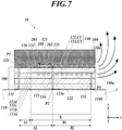
- FIG. 7 is a sectional view showing the configuration of the RFID tag 10 of the second embodiment.
- FIG. 8 is an exploded perspective view of the RFID tag 10 shown in FIG. 7 .
- the capacitance conductor 123 faces part of the upper surface conductor 121 to form the capacitance element 140 together with the upper surface conductor 121. That is, the first conductor C1 of the capacitance element 140 is constituted by the upper surface conductor 121, and the second conductor C2 thereof is constituted by the capacitance conductor 123.
- the capacitance part through conductor 132 is disposed in layers of the insulating substrate 110 between the capacitance conductor 123 and the lower surface conductor 122 (i.e. passes through the stacking substrates 111a to 111c in the z direction) to electrically connect the capacitance conductor 123 and the lower surface conductor 122.
- the first electrode 124 is electrically connected to the upper surface conductor 121 by a connection electrode 126 disposed, of the upper surface 110a of the insulating substrate 110, in a region that connects the first electrode 124 and the upper surface conductor 121.
- a connection electrode 126 disposed, of the upper surface 110a of the insulating substrate 110, in a region that connects the first electrode 124 and the upper surface conductor 121.
- the upper surface conductor 121 constitutes the radiation conductor of the plate-like inverted-F antenna
- the capacitance conductor 123, the capacitance part through conductor 132 and the lower surface conductor 122 constitute the ground conductor of the plate-like inverted-F antenna.
- connection point where the connection electrode 126 and the upper surface conductor 121 are connected corresponds to the connection point P1
- connection point where the interlayer through conductor 134 and the lower surface conductor 122 are connected corresponds to the connection point P2.
- the distance A1 between the connection point P1 and the short-circuit part through conductor 131 is shorter than the distance A2 between the connection point P2 and the short-circuit part through conductor 131.
- the distance B1 between the connection point P1 and the capacitance part through conductor 132 is longer than the distance B2 between the connection point P2 and the capacitance part through conductor 132.
- the capacitance conductor 123 faces at least part of the upper surface conductor 121 to form the capacitance element 140.
- the position of the open end part 140a of the pair of the conductors of the capacitance element 140 i.e. a position where radio waves are mainly emitted from the plate-like inverted-F antenna
- the position where radio waves are emitted can be immediately below the sealing member 300.
- Radio waves emitted from this position in the +x direction hardly enter the sealing member 300 because the distance from the position to the sealing member 300 is extremely short. This is because radio waves require some space to turn their traveling direction (i.e. because radio waves cannot turn sharply in a narrow space). As a result, the emitted radio waves are hardly affected by the sealing member 300, and hence the communication distance can be longer.
- the first conductor C1 is the upper surface conductor 121 and the second conductor C2 is the capacitance conductor 123
- the second electrode 125 is electrically connected to the lower surface conductor 122 via the second interlayer through conductor that passes through the insulating substrate 110
- the distance A1 from the electrical connection point P1 on the upper surface conductor 121 with the first electrode 124 to the short-circuit part through conductor 131 is shorter than the distance A2 from the electrical connection point P2 on the lower surface conductor 122 with the second electrode 125 to the short-circuit part through conductor 131.
- connection point P1 which is the end part position on the short-circuit part through conductor 131 side of the section R, closer to the short-circuit part through conductor 131, the section R can be made long.
- the potential difference generated between the conductors, which are a pair of conductors, of the capacitance element 140 can be larger, the intensity of the radio waves to be emitted can be higher, and the communication distance can be longer.
- the distance B1 from the electrical connection point P1 on the upper surface conductor 121 with the first electrode 124 to the capacitance part through conductor 132 is longer than the distance B2 from the electrical connection point P2 on the lower surface conductor 122 with the second electrode 125 to the capacitance part through conductor 132.
- the connection point P3 where the capacitance part through conductor 132 and the lower surface conductor 122 are connected can be greatly away from the connection point P1 where the first electrode 124 and the capacitance conductor 123 are connected.
- a simple layer structure can make the section R longer.
- connection point P2 where the second electrode 125 and the ground conductor are connected is different from that in the second embodiment.
- the same components as those of the second embodiment are denoted by the same reference signs, and detailed descriptions thereof are omitted.
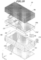
- FIG. 9 is a sectional view showing the configuration of the RFID tag 10 of the third embodiment.
- FIG. 10 is an exploded perspective view of the RFID tag 10 shown in FIG. 9 .
- the capacitance conductor 123 is electrically connected to the second electrode 125 by an interlayer through conductor 135 (third interlayer through conductor).
- the interlayer through conductor 135 is disposed in a layer of the insulating substrate 110 between the second electrode 125 and the capacitance conductor 123 (i.e. passes through the stacking substrate 111d in the z direction).
- the interlayer through conductor 135 is disposed so as to be superposed on the second electrode 125 when viewed in the z direction.
- connection point where the interlayer through conductor 135 and the capacitance conductor 123 are connected corresponds to the connection point P2, and the connection point P1 is the same as that in the second embodiment.
- the distance A1 between the connection point P1 and the short-circuit part through conductor 131 is shorter than the distance A2 between the connection point P2 and the short-circuit part through conductor 131. Also, the distance B1 between the connection point P1 and the capacitance part through conductor 132 is longer than the distance B2 between the connection point P2 and the capacitance part through conductor 132.
- the first conductor C1 is the upper surface conductor 121 and the second conductor C2 is the capacitance conductor 123
- the second electrode 125 is electrically connected to the capacitance conductor 123 via the third interlayer through conductor that is disposed in a layer of the insulating substrate 110 between the second electrode 125 and the capacitance conductor 123
- the distance A1 from the electrical connection point P1 on the upper surface conductor 121 with the first electrode 124 to the short-circuit part through conductor 131 is shorter than the distance A2 from the electrical connection point P2 on the capacitance conductor 123 with the second electrode 125 to the short-circuit part through conductor 131.
- a simple layer structure can make the section R, in which charges accumulate, of the capacitance element 140 longer. More specifically, by making the connection point P1, which is the end part position on the short-circuit part through conductor 131 side of the section R, closer to the short-circuit part through conductor 131, the section R can be made long. Thus, the potential difference generated between the conductors, which are a pair of conductors, of the capacitance element 140 can be larger, the intensity of the radio waves to be emitted can be higher, and the communication distance can be longer.
- the distance B1 from the electrical connection point P1 on the upper surface conductor 121 with the first electrode 124 to the capacitance part through conductor 132 is longer than the distance B2 from the electrical connection point P2 on the capacitance conductor 123 with the second electrode 125 to the capacitance part through conductor 132.
- the connection point P3 where the capacitance part through conductor 132 and the lower surface conductor 122 are connected can be greatly away from the connection point P1 where the first electrode 124 and the capacitance conductor 123 are connected.
- a simple layer structure can make the section R longer.
- the capacitance conductor 123 faces the upper surface conductor 121, the capacitance element 140 is disposed immediately below the sealing member 300 (i.e. radio waves radiate from immediately below the sealing member 300), and electrical connection between the second electrode 125 and the ground conductor is performed by the interlayer through conductor 135 that passes through the layer between the second electrode 125 and the capacitance conductor 123 only.
- the capacitance conductor 123 faces part of the upper surface conductor 121 or part of the lower surface conductor 122, but is not limited thereto.
- the capacitance conductor 123 may face the entire upper surface conductor 121 or the entire lower surface conductor 122.
- the RFID tag board 100 is a rectangular parallelepiped that is long in the x direction, but is not limited thereto.
- the RFID tag board 100 may be square when viewed in the z direction or long in the y direction.
- the insulating substrate 110 is composed of the four stacking substrates 111a to 111d, but is not limited thereto.
- the insulating substrate 110 may be composed of three or less stacking substrates or five or more stacking substrates.
- the present disclosure is applicable to an RFID tag board, an RFID tag and an RFID system.
Landscapes
- Engineering & Computer Science (AREA)
- Computer Hardware Design (AREA)
- Microelectronics & Electronic Packaging (AREA)
- Physics & Mathematics (AREA)
- General Physics & Mathematics (AREA)
- Theoretical Computer Science (AREA)
- Computer Networks & Wireless Communication (AREA)
- Details Of Aerials (AREA)
- Waveguide Aerials (AREA)
Abstract
Description
- The present disclosure relates to an RFID (Radio Frequency Identifier) tag board, an RFID tag and an RFID system.
- For the purpose of, for example, article management, an RFID system is used conventionally that transmits and receives information with an RFID tag(s) to and from an article(s) by wireless communication. As the RFID tag, an RFID tag having an RFID tag board provided with an antenna, such as a plate-like inverted-F antenna, and a semiconductor integrated circuit mounted on a plate surface of the RFID tag board is widely used (e.g.
WO 2013/145312 A1 ). Via the antenna of the RFID tag board, the RFID tag can transmit radio waves containing information stored in the semiconductor integrated circuit and also write information contained in received radio waves into the semiconductor integrated circuit. According to an RFID system using such an RFID tag(s), for example, an RFID tag is attached to an article, and a predetermined reader/writer obtains information on the article from the RFID tag or writes necessary information into the RFID tag. Thus, articles can be managed. - An RFID tag board of an aspect of the present disclosure has a plate surface on which a semiconductor integrated circuit is to be mounted, is used with the plate surface and the semiconductor integrated circuit thereon sealed with a sealing member, and includes:
- an insulating substrate one surface of which forms the plate surface;
- a first surface conductor that is disposed on the one surface of the insulating substrate;
- a second surface conductor that is disposed on a surface of the insulating substrate opposite to the one surface;
- a short-circuit part through conductor that passes through the insulating substrate in a thickness direction to electrically connect the first surface conductor and the second surface conductor;
- a capacitance conductor that is disposed in the insulating substrate and faces at least part of the first surface conductor or at least part of the second surface conductor to form a capacitance element;
- a capacitance part through conductor that is disposed in the insulating substrate to electrically connect the capacitance conductor and one of the first surface conductor and the second surface conductor not facing the capacitance conductor;
- a first electrode that is disposed on the one surface of the insulating substrate and to which, among terminals that the semiconductor integrated circuit has, a terminal from which a voltage signal relating to a transmission radio wave is output is electrically connected; and
- a second electrode that is disposed on the one surface of the insulating substrate and to which, among the terminals that the semiconductor integrated circuit has, a terminal serving as a reference potential is electrically connected,
- wherein a first conductor of a pair of conductors that forms the capacitance element is electrically connected to the first electrode not via the short-circuit part through conductor, and a second conductor of the pair of conductors is electrically connected to the second electrode not via the short-circuit part through conductor, and
- wherein a distance from the first electrode to the short-circuit part through conductor is shorter than a distance from the second electrode to the short-circuit part through conductor.
- An RFID tag of an aspect of the present disclosure includes:
- the above RFID tag board;
- the semiconductor integrated circuit that is mounted on the plate surface of the RFID tag board; and
- the sealing member with which the plate surface of the RFID tag board and the semiconductor integrated circuit thereon are sealed.
- An RFID system of an aspect of the present disclosure includes:
- the above RFID tag; and
- a reader/writer that transmits and receives a radio wave to and from the RFID tag.
- According to the present disclosure, there is an effect of making a communication distance long.
-
-
FIG. 1 shows an RFID system. -
FIG. 2A is a diagram for explaining the radiation state of radio waves due to the structure of an RFID tag. -
FIG. 2B is a diagram for explaining the radiation state of radio waves due to the structure of an RFID tag. -
FIG. 3 is a sectional view showing the configuration of an RFID tag of a first embodiment. -
FIG. 4 is an exploded perspective view of the RFID tag shown inFIG 3 . -
FIG. 5 is an exploded perspective view showing another aspect of the RFID tag of the first embodiment. -
FIG. 6 is a sectional view showing the configuration of an RFID tag board of a comparative example. -
FIG. 7 is a sectional view showing the configuration of an RFID tag of a second embodiment. -
FIG. 8 is an exploded perspective view of the RFID tag shown inFIG. 7 . -
FIG. 9 is a sectional view showing the configuration of an RFID tag of a third embodiment. -
FIG. 10 is an exploded perspective view of the RFID tag shown inFIG. 9 . - Hereinafter, embodiments of the present disclosure will be described in detail with reference to the drawings.
-
FIG. 1 shows an RFID system 1 according to a first embodiment of the present disclosure. - The RFID system 1 includes an
RFID tag 10 and a reader/writer 2 that transmits and receives radio waves to and from theRFID tag 10. - The
RFID tag 10 is used, for example, by being attached to the surface of anarticle 3 to manage. TheRFID tag 10 is a type having no built-in battery, and receives electric power from the reader/writer 2 via electromagnetic waves and operates by this electric power. TheRFID tag 10 may be a type having a built-in battery. - The
RFID tag 10 includes anRFID tag board 100, an RFID tag IC (Integrated Circuit) 200 (semiconductor integrated circuit) mounted on a plate surface of theRFID tag board 100, and asealing member 300 for sealing the plate surface, on which theRFID tag IC 200 is mounted, of theRFID tag board 100 and the RFID tag IC 200. - The
RFID tag board 100 is a rectangular-parallelepiped-shaped plate-like member in which a plate-like inverted-F antenna is formed. The configuration thereof will be described later in detail. - The RFID tag IC 200 includes a controller that performs control about transmission and reception of radio waves, a storage that stores, for example, information on the
article 3, and a feeding terminal 201 (shown inFIG. 3 ) and a reference potential terminal 202 (shown inFIG. 3 ) that are electrically connected to the antenna of theRFID tag board 100. Under the control of the controller, theRFID tag IC 200 obtains instruction information contained in radio waves received by the antenna and performs a process corresponding to the instruction information (e.g. rewrites information stored in the storage), and also causes the antenna to transmit (radiate) radio waves containing information specified by the instruction information. - The sealing
member 300 covers and protects theRFID tag IC 200. The sealingmember 300 is molded such that a structural body composed of theRFID tag board 100 and the sealingmember 300 becomes a rectangular parallelepiped as a whole. As the sealingmember 300, for example, epoxy resin, polyimide resin, silicone resin or the like is usable. Filler particles, such as silica particles or glass particles, may be added to any of these resin materials. The filler particles are added thereto in order to adjust various characteristics, such as mechanical strength, moisture resistance and electrical characteristics, of thesealing member 300, for example. - The reader/
writer 2 has anantenna 2a for transmitting and receiving radio waves to and from theRFID tag 10. The reader/writer 2 transmits, to theRFID tag 10, radio waves containing instruction information instructing theRFID tag 10 to rewrite information or transmit information. Also, the reader/writer 2 receives radio waves transmitted from theRFID tag 10 in accordance with the instruction information, obtains information contained in the radio waves, and performs a predetermined process by using the information (e.g. a process of writing the information into a predetermined storage device or a process of displaying the information on a predetermined display device). -
FIG. 2A and FIG. 2B are each a diagram for explaining the radiation state of radio waves due to the structure of anRFID tag 10. - As RFID tags, there are a cavity-
type RFID tag 10C as shown inFIG. 2A and a plate-type RFID tag 10 as shown inFIG. 1 orFIG. 2B . In this embodiment, the plate-type RFID tag 10 is used. - In
FIG. 2A and FIG. 2B , a Cartesian coordinate system x, y, z defined fixedly to theRFID tag 10C and theRFID tag 10 is shown. The z direction may be referred to as a height direction of theRFID tag 10C and theRFID tag 10. Herein, the height is merely a designation for the sake of convenience, and hence the height direction herein does not always coincide with the actual height direction (vertical direction) of theRFID tag 10C and theRFID tag 10 when used. The same applies to the Cartesian coordinate system shown inFIG. 3 and the following figures. - In the cavity-
type RFID tag 10C shown inFIG. 2A , a recess (cavity) is provided in the upper surface of theRFID tag board 100, theRFID tag IC 200 is mounted on the bottom surface of the recess, and the inside of the recess is sealed with the sealingmember 300. - Meanwhile, in the plate-
type RFID tag 10 shown inFIG. 2B , as described with reference toFIG. 1 , the entire upper surface of the plate-likeRFID tag board 100 is sealed with the plate-like sealing member 300. The plate-type RFID tag 10 can be manufactured at lower cost than the cavity-type RFID tag 10C because it does not require a step of forming a recess in theRFID tag board 100, and also can be manufactured efficiently, for example, by a method of forming the sealingmember 300 on the entire surface of a compound substrate containing a large number ofRFID tag boards 100 and then dividing it. - In each of the cavity-
type RFID tag 10C and the plate-type RFID tag 10, radio waves that are transmitted from theRFID tag board 100 radiate from a side surface (one of the surfaces parallel to the yz plane) of theRFID tag board 100 and travel so as to go around in the +z direction. A radio-wave transmittable distance from the mounting surface, on which theRFID tag 10/10C is mounted, of thearticle 3 in the +z direction depends on the magnitude of electric power received from the reader/writer 2, the size of theRFID tag 10/10C and so forth, but is usually within a range of about several tens of centimeters to several meters. - Radio waves have a property of passing through a substance having a higher permittivity (relative permittivity or relative dielectric constant). Hence, in the plate-
type RFID tag 10 shown inFIG. 2B , radio waves radiated from the side surface of theRFID tag board 100 to the outer space are likely to enter, in part, the sealingmember 300, and radiate less in a desired direction (+z direction). Meanwhile, in the cavity-type RFID tag 10C shown inFIG. 2A , because the sealingmember 300 is embedded in the recess, radio waves are unlikely to enter the sealingmember 300, and hardly cause the above problem. - Hence, when
RFID tag boards 100 have the same structure (except for the presence or absence of a recess), a radio-wave reaching distance L2 from the plate-type RFID tag 10 in the +z direction tends be shorter than a radio-wave reaching distance L1 from the cavity-type RFID tag 10C in the +z direction. That is, the plate-type RFID tag 10 is likely to have a shorter communication distance than the cavity-type RFID tag 10C has. - To deal with this problem, in the
RFID tag 10 of this embodiment, while the plate-type structure is adopted to hold down manufacturing cost, the configuration of theRFID tag board 100 is optimized to make the communication distance longer. Hereinafter, the configuration of theRFID tag 10 of this embodiment will be described with the focus on the structure of theRFID tag board 100. -
FIG. 3 is a sectional view showing the configuration of theRFID tag 10 of this embodiment. -
FIG. 4 is an exploded perspective view of theRFID tag 10 shown inFIG. 3 . - As shown in
FIG. 3 andFIG. 4 , the RFID tag board 100 includes: an insulating substrate 110; an upper surface conductor 121 (first surface conductor), a first electrode 124 and a second electrode 125 disposed on one surface of the insulating substrate 110 (surface facing to the +z direction, which hereinafter may be referred to as an upper surface 110a); a lower surface conductor 122 (second surface conductor) disposed on the opposite surface of the insulating substrate 110 (surface facing to the -z direction, which hereinafter may be referred to as a lower surface 110b) to the one surface; a capacitance conductor 123 disposed in the insulating substrate 110 and facing part of the lower surface conductor 122 to form a capacitance element 140 (capacitor) together with the lower surface conductor 122; a short-circuit part through conductor 131 passing through the insulating substrate 110 in the thickness direction and electrically connecting the upper surface conductor 121 and the lower surface conductor 122; a capacitance part through conductor 132 disposed in the insulating substrate 110 and electrically connecting the capacitance conductor 123 and the upper surface conductor 121; an interlayer through conductor 133 (first interlayer through conductor) disposed in the insulating substrate 110 and electrically connecting the first electrode 124 and the capacitance conductor 123; and an interlayer through conductor 134 (second interlayer through conductor) passing through the insulating substrate 110 in the thickness direction and electrically connecting the second electrode 125 and the lower surface conductor 122. - The
RFID tag board 100 is attached and fixed to thearticle 3 such that thelower surface 110b (lower surface conductor 122) of the insulatingsubstrate 110 faces thearticle 3. TheRFID tag 10 of this embodiment operates even when the surface of thearticle 3 is formed of a conductor, such as metal. That is, when theRFID tag board 100 is attached to such anarticle 3, the conductive portion of thearticle 3 also functions as a ground conductor of the antenna of theRFID tag 10. - The
RFID tag IC 200 is mounted on the upper surface of the insulatingsubstrate 110. The upper surface of the insulatingsubstrate 110 and theRFID tag IC 200 thereon are covered and sealed with the sealingmember 300. That is, the upper surface of the insulatingsubstrate 110 constitutes the above-described plate surface, on which theRFID tag IC 200 is mounted and which is sealed with the sealingmember 300, of theRFID tag board 100. - The insulating
substrate 110 is a plate-like member having a structure in which two or more (four in this embodiment) stackingsubstrates 111a to 111d formed of a dielectric (ceramic in this embodiment) are stacked in this order from the bottom. The insulatingsubstrate 110 has theupper surface 110a and thelower surface 110b that are parallel to the xy plane, and is a rectangular parallelepiped the height (length in the z direction) of which is shorter than the width dimension (length in the x direction) and the depth dimension (length in the y direction), and the width dimension of which is longer than the depth dimension, thereby being long in the x direction. The stackingsubstrates 111a to 111d constituting the insulatingsubstrate 110 may be formed of, for example, a dielectric, such as an aluminum oxide sintered body, an aluminum nitride sintered body, a mullite sintered body or a glass-ceramic sintered body. The insulatingsubstrate 110 may be formed by stacking two or more (four in this embodiment) sheet-shaped layers (four layers in this embodiment) of ceramic green sheets on top of one another and then firing/sintering these. - On the
upper surface 110a of the insulatingsubstrate 110, thefirst electrode 124 and thesecond electrode 125 that are rectangular when viewed in the +z direction are disposed. The shape of thefirst electrode 124 and thesecond electrode 125 is not limited to a rectangle, and may be another polygon, a circle or the like. - The
first electrode 124 is electrically connected via a bonding wire to, among terminals that theRFID tag IC 200 has, the feeding terminal 201 from which a voltage signal(s) relating to transmission radio waves is output. Thefirst electrode 124 is disposed on the -x direction side as compared with thesecond electrode 125. - The
second electrode 125 is electrically connected via a bonding wire to, among the terminals that theRFID tag IC 200 has, the referencepotential terminal 202 that serves as a reference potential. The reference potential of this embodiment is a ground potential, and the referencepotential terminal 202 is a ground terminal. The reference potential is not limited to the ground potential, and a predetermined potential other than the ground potential may be used as the reference potential. - The method of connecting the
first electrode 124 and thesecond electrode 125 to the above-described terminals of theRFID tag IC 200 is not limited to the method using bonding wires, and they may be connected, for example, by flip chip mounting. - On the
upper surface 110a of the insulatingsubstrate 110, theupper surface conductor 121 is disposed. Theupper surface conductor 121 is a plate-like conductor that is long in the x direction, and is disposed on almost the entireupper surface 110a of the insulatingsubstrate 110 except a region where thefirst electrode 124 and thesecond electrode 125 are formed. That is, theupper surface conductor 121 has a shape having anopening 121a for ensuring the region where thefirst electrode 124 and thesecond electrode 125 are formed. - The
lower surface conductor 122 is a plate-like conductor that is long in the x direction, and is disposed on almost the entirelower surface 110b of the insulatingsubstrate 110. - The
capacitance conductor 123 is a plate-like conductor disposed between the lowermost stackingsubstrate 111a and the secondlowermost stacking substrate 111b of the insulatingsubstrate 110, and faces part of thelower surface conductor 122 to form thecapacitance element 140. That is, when a pair of conductors forming thecapacitance element 140 is a first conductor C1 and a second conductor C2, the first conductor C1 on the +z direction side is constituted by thecapacitance conductor 123, and the second conductor C2 on the -z direction side is constituted by thelower surface conductor 122. Thecapacitance conductor 123 has acircular opening 123a for allowing the interlayer throughconductor 134 to pass through. Theopening 123a is formed with a size that ensures a clearance of a predetermined distance from the interlayer throughconductor 134. - The
upper surface conductor 121, thelower surface conductor 122, thecapacitance conductor 123, thefirst electrode 124 and thesecond electrode 125 can be formed by, at a stage where the stackingsubstrates 111a to 111d are ceramic green sheets, printing metal paste at their positions on the ceramic green sheets by screen printing or another method, and firing these together. More specifically, first, metal paste for thelower surface conductor 122 is printed on the lower surface of a ceramic green sheet for the stackingsubstrate 111a, and metal paste for thecapacitance conductor 123 is printed on the lower surface of a ceramic green sheet for the stackingsubstrate 111b. Alternatively, metal paste for thecapacitance conductor 123 may be printed on the upper surface of a ceramic green sheet for the stackingsubstrate 111a, and metal paste for thelower surface conductor 122 may be printed on the lower surface thereof. In addition, metal paste for theupper surface conductor 121, thefirst electrode 124 and thesecond electrode 125 is printed on the upper surface of a ceramic green sheet for the stackingsubstrate 111d. Next, the four ceramic green sheets for the stackingsubstrates 111a to 111d are stacked and then fired as a whole. Thus, theupper surface conductor 121, thelower surface conductor 122, thecapacitance conductor 123, thefirst electrode 124 and thesecond electrode 125 can be formed on/in the insulatingsubstrate 110. - As the metal paste, for example, a mixed material of copper powder with an organic solvent and an organic binder is usable. The exposed surfaces of the
upper surface conductor 121, thelower surface conductor 122, thefirst electrode 124 and thesecond electrode 125 may be coated with plating layers formed of, for example, nickel, cobalt, palladium or gold. This can inhibit oxidation corrosion. Thefirst electrode 124 and thesecond electrode 125 coated with a plating layer(s) also improve their joining characteristics with the bonding wires. - The short-circuit part through
conductor 131 passes through layers between theupper surface 110a and thelower surface 110b of the insulatingsubstrate 110 in the z direction to electrically connect theupper surface conductor 121 and thelower surface conductor 122. The short-circuit part throughconductor 131 is disposed at the end part on the -x direction side in the longer direction (x direction) of the insulatingsubstrate 110. Hence, the short-circuit part throughconductor 131 is connected to the end parts on the -x direction side in the longer direction (x direction) of theupper surface conductor 121 and thelower surface conductor 122. An end part in the longer direction of the insulatingsubstrate 110 is, for example, a region having a length of 10% or less of the length of the insulatingsubstrate 110 in the longer direction from an end in the longer direction. The short-circuit part throughconductor 131 has widths in the x direction and the y direction narrower than each of theupper surface conductor 121 and thelower surface conductor 122 has, and is pin-shaped in this embodiment. - The capacitance part through
conductor 132 is disposed in layers of the insulatingsubstrate 110 between theupper surface conductor 121 and the capacitance conductor 123 (i.e. passes through the stackingsubstrates 111b to 111d in the z direction) to electrically connect theupper surface conductor 121 and thecapacitance conductor 123. The capacitance part throughconductor 132 is disposed at the end part on the +x direction side in the longer direction of the insulatingsubstrate 110. Hence, the capacitance part throughconductor 132 is connected to the end parts on the +x direction side in the longer direction of theupper surface conductor 121 and thecapacitance conductor 123. Similarly to the short-circuit part throughconductor 131, the capacitance part throughconductor 132 has widths in the x direction and the y direction narrower than each of theupper surface conductor 121 and thelower surface conductor 122 has, and is pin-shaped in this embodiment. - In the
RFID tag 10 shown inFIG. 3 andFIG. 4 , one short-circuit part throughconductor 131 and one capacitance part throughconductor 132 are provided. However, as shown inFIG. 5 , a plurality of short-circuit part throughconductors 131 may be disposed at the end part on the -x direction side of the insulatingsubstrate 110, and a plurality of short-circuit part throughconductors 131 may be disposed at the end part on the +x direction side of the insulatingsubstrate 110. Alternatively, for only one of the short-circuit part throughconductor 131 and the capacitance part throughconductor 132, a plurality of conductors may be provided. - The interlayer through
conductor 133 is disposed in layers of the insulatingsubstrate 110 between thefirst electrode 124 and the capacitance conductor 123 (i.e. passes through the stackingsubstrate 111b to 111d in the z direction) to electrically connect thefirst electrode 124 and thecapacitance conductor 123. The interlayer throughconductor 133 is disposed so as to be superposed on thefirst electrode 124 when viewed in the z direction. - The interlayer through
conductor 134 passes through layers between theupper surface 110a and thelower surface 110b of the insulatingsubstrate 110 in the z direction to electrically connect thesecond electrode 125 and thelower surface conductor 122. The interlayer throughconductor 134 is disposed so as to be superposed on thesecond electrode 125 when viewed in the z direction. Also, the interlayer throughconductor 134 is disposed so as to pass through theopening 123a of thecapacitance conductor 123. - Similarly to the short-circuit part through
conductor 131, the interlayer throughconductors upper surface conductor 121 and thelower surface conductor 122 has, and are pin-shaped in this embodiment. - The short-circuit part through
conductor 131, the capacitance part throughconductor 132 and the interlayer throughconductors substrates 111a to 111d are ceramic green sheets, the stage being before metal paste is printed to form theupper surface conductor 121 and so forth, providing through holes or interlayer holes in the ceramic green sheets, filling the holes with the metal paste, and firing these together. As the metal paste, as with the material for theupper surface conductor 121, for example, a mixed material of copper powder with an organic solvent and an organic binder is usable. - In thus-configured
RFID tag board 100, theupper surface conductor 121, thelower surface conductor 122, thecapacitance conductor 123, the short-circuit part throughconductor 131, the capacitance part throughconductor 132 and the interlayer throughconductors upper surface conductor 121, thecapacitance conductor 123 and the capacitance part throughconductor 132 acts as a radiation conductor of the plate-like inverted-F antenna, and thelower surface conductor 122 acts as a ground conductor (which may be referred to as a ground plane or a reference potential conductor) of the plate-like inverted-F antenna. The short-circuit part throughconductor 131 acts as an electrical wall of the plate-like inverted-F antenna, the interlayer throughconductor 133 acts as a feeder of the plate-like inverted-F antenna, and the interlayer throughconductor 134 acts as a ground of the plate-like inverted-F antenna. - As shown in
FIG. 3 , in this plate-like inverted-F antenna, radio waves mainly radiate from anopen end part 140a on the +x direction side of the pair of the conductors of thecapacitance element 140. After radiating to the +x direction side, the radio waves travel so as to go around to the +z direction side. - A plate-like inverted-F antenna electrically corresponds to a patch antenna having a shape in which a radiation conductor and a short-circuit conductor on the +x direction side of an electrical wall extend to the other side (-x direction side) of the electrical wall, with the electrical wall as an axis of symmetry. That is, according to the configuration of a plate-like inverted-F antenna in which a radiation conductor and a short-circuit conductor are connected by an electrical wall, the area thereof can be reduced by half the area of a patch antenna having the same function. The plate-like inverted-F antenna of this embodiment has a wavelength shortening effect by part (capacitance conductor 123) of the radiation conductor and part of the short-circuit conductor (lower surface conductor 122) forming the
capacitance element 140. This also contributes to miniaturization. - Hereinafter, on the radiation conductor of the plate-like inverted-F antenna, a point where electrical connection with the
first electrode 124 is performed is referred to as a connection point P1. In this embodiment, the connection point P1 is a point where thecapacitance conductor 123 and the interlayer throughconductor 133 are connected (electrical connection point on thecapacitance conductor 123 with the first electrode 124). The interlayer throughconductor 133 extends from thefirst electrode 124 in the - z direction, and hence in the x direction and the y direction, the connection point P1 is the same as the position of thefirst electrode 124. - Hereinafter, on the ground conductor of the plate-like inverted-F antenna, a point where electrical connection with the
second electrode 125 is performed is referred to as a connection point P2. In this embodiment, the connection point P2 is a point where thelower surface conductor 122 and the interlayer throughconductor 134 are connected (electrical connection point on thelower surface conductor 122 with the second electrode 125). The interlayer throughconductor 134 extends from thesecond electrode 125 in the -z direction, and hence in the x direction and the y direction, the connection point P2 is the same as the position of thesecond electrode 125. - In the
RFID tag board 100 of this embodiment, as described above, thefirst electrode 124 is disposed on the -x direction side as compared with thesecond electrode 125. Hence, the connection point P1 is located on the -x direction side as compared with the connection point P2. - Because the
first electrode 124 and thesecond electrode 125 have the above-described positional relationship, a distance A1 between thefirst electrode 124 and the short-circuit part throughconductor 131 is shorter than a distance A2 between thesecond electrode 125 and the short-circuit part throughconductor 131. In other words, the distance A1 between the connection point P1 and the short-circuit part throughconductor 131 is shorter than the distance A2 between the connection point P2 and the short-circuit part throughconductor 131. - Also, a distance B1 between the
first electrode 124 and the capacitance part throughconductor 132 is longer than a distance B2 between thesecond electrode 125 and the capacitance part throughconductor 132. In other words, the distance B1 between the connection point P1 and the capacitance part throughconductor 132 is longer than the distance B2 between the connection point P2 and the capacitance part throughconductor 132. - In the plate-like inverted-F antenna of the
RFID tag board 100, during operation of the antenna, current mainly flows, of the first conductor C1 (capacitance conductor 123) of thecapacitance element 140, in a section R that is from the connection point P1 with the interlayer through conductor 133 (feeder) to a connection point with the capacitance part through conductor 132 (which is hereinafter referred to as a connection point P3). Hence, in this section R, charges having the opposite polarities accumulate on the first conductor C1 and the second conductor C2 of thecapacitance element 140.FIG. 3 shows that positive charges accumulate on the first conductor C1 and negative charges accumulate on the second conductor C2. However, because AC voltage signals are output from the feed terminal of theRFID tag IC 200, the polarities of charges that accumulate on thecapacitance element 140 are reversed from those shown inFIG. 3 depending on the period of time. - In the
RFID tag board 100 of this embodiment, the connection point P1 is closer to the short-circuit part throughconductor 131 than the connection point P2 is. This can ensure a longer section R. Advantages of this configuration will be described in comparison with the configuration of anRFID tag board 100r of a comparative example. -
FIG. 6 is a sectional view showing the configuration of theRFID tag board 100r of the comparative example. - In the
RFID tag board 100r of this comparative example, the positional relationship in the x direction between thefirst electrode 124 and thesecond electrode 125 is reversed from that in theRFID tag board 100 shown inFIG. 3 . Hence, the positional relationship in the x direction between the interlayer through conductor 133 (feeder) and the interlayer through conductor 134 (ground) is also reversed from that in theRFID tag board 100 shown inFIG. 3 . As a result, the distance A1 between the connection point P1 and the short-circuit part throughconductor 131 is longer than the distance A2 between the connection point P2 and the short-circuit part throughconductor 131. Also, the distance B1 between the connection point P1 and the capacitance part throughconductor 132 is shorter than the distance B2 between the connection point P2 and the capacitance part throughconductor 132. - In thus-configured
RFID tag board 100r of the comparative example, the section R from the connection point P1 to the connection point P3, in which current flows during operation of the antennas, is shorter than the section R in theRFID tag board 100 shown inFIG. 3 . Hence, charges accumulate less on thecapacitance element 140. - Conversely, in the
RFID tag board 100 of the embodiment shown inFIG. 3 , the section R, in which charges accumulate, of thecapacitance element 140 is longer than the section R in theRFID tag board 100r of the comparative example shown inFIG. 6 . Thus, as compared with the comparative example, more charges accumulate on thecapacitance element 140, and the potential difference generated between the conductors, which are a pair of conductors, of thecapacitance element 140 can be larger. As a result, stronger radio waves are emitted from the plate-like inverted-F antenna, and hence a radio wave transmission distance, namely, the communication distance, can be longer. - As described above, the RFID tag board 100 has a plate surface on which the RFID tag ID 200 is to be mounted, is used with the plate surface and the RFID tag ID 200 thereon sealed with the sealing member 300, and includes: the insulating substrate 100 one surface of which forms the plate surface; the upper surface conductor 121 that is disposed on the one surface of the insulating substrate 110; the lower surface conductor 122 that is disposed on the surface of the insulating substrate 110 opposite to the one surface; the short-circuit part through conductor 131 that passes through the insulating substrate 110 in the thickness direction to electrically connect the upper surface conductor 121 and the lower surface conductor 122; the capacitance conductor 123 that is disposed in the insulating substrate 110 and faces at least part of the lower surface conductor 122 to form the capacitance element 140; the capacitance part through conductor 132 that is disposed in the insulating substrate 110 to electrically connect the capacitance conductor 123 and the upper surface conductor 121; the first electrode 124 that is disposed on the one surface of the insulating substrate 110 and to which, among terminals that the RFID tag IC 200 has, a terminal from which a voltage signal (s) relating to a transmission radio wave(s) is output is electrically connected; and the second electrode 125 that is disposed on the one surface of the insulating substrate 110 and to which, among the terminals that the RFID tag IC 200 has, a terminal serving as a reference potential is electrically connected, wherein the first conductor C1 (capacitance conductor 123) of a pair of conductors that forms the capacitance element 140 is electrically connected to the first electrode 124 not via the short-circuit part through conductor 131, and the second conductor C2 (lower surface conductor 122) of the pair of conductors is electrically connected to the second electrode 125 not via the short-circuit part through conductor 131, and the distance A1 from the first electrode 124 to the short-circuit part through conductor 131 is shorter than the distance A2 from the second electrode 125 to the short-circuit part through conductor 131.
- According to this configuration, the connection point P1 where the
first electrode 124 and the capacitance conductor 123 (radiation conductor) are connected can be easily provided closer to the short-circuit part throughconductor 131 than the connection point P2 where thesecond electrode 125 and the lower surface conductor 122 (ground conductor) are connected is. That is, by a simple configuration in which the interlayer throughconductors substrate 110 connect conductors, the distance A1 from the connection point P1 to the short-circuit part throughconductor 131 can be made shorter than the distance A2 from the connection point P2 to the short-circuit part throughconductor 131. - By the connection point P1 and the connection point P2 having this positional relationship, the section R, in which charges accumulate, of the
capacitance element 140 can be made long. More specifically, by making the connection point P1, which is the end part position on the short-circuit part throughconductor 131 side of the section R, closer to the short-circuit part throughconductor 131, the section R can be made long. Thus, more charges accumulate on thecapacitance element 140, and the potential difference generated between the conductors, which are a pair of conductors, of thecapacitance element 140, can be larger. As a result, stronger radio waves can be emitted from the plate-like inverted-F antenna. - Further, because the connection point P2 where the
second electrode 125 and the lower surface conductor 122 (ground conductor) are connected is close to theopen end part 140a of thecapacitance element 140, the potential (reference potential) on thelower surface conductor 122 side of theopen end part 140a can be more stable. This can also make radio waves that are emitted from the plate-like inverted-F antenna stronger. - As described above, according to the configuration of this embodiment, stronger radio waves are emitted from the plate-like inverted-F antenna. Hence, even in the configuration in which the
upper surface 110a of the insulatingsubstrate 110 is sealed with the sealingmember 300, the radio wave transmission distance, namely, the communication distance, can be longer. - Further, the distance B1 from the
first electrode 124 to the capacitance part throughconductor 132 is longer than the distance B2 from thesecond electrode 125 to the capacitance part throughconductor 132. According to this configuration, the connection point P3 where the capacitance part throughconductor 132 and thecapacitance conductor 123 are connected can be greatly away from the connection point P1 where thefirst electrode 124 and thecapacitance conductor 123 are connected. Hence, the section R having the connection point P1 and the connection point P3 as the ends can be longer. Thus, the potential difference generated between the conductors, which are a pair of conductors, of thecapacitance element 140 can be larger, the intensity of the radio waves to be emitted can be higher, and the communication distance can be longer. - Further, the
capacitance conductor 123 faces at least part of thelower surface conductor 122 to form thecapacitance element 140, the first conductor C1 of thecapacitance element 140 is thecapacitance conductor 123 and the second conductor C2 thereof is thelower surface conductor 122, thefirst electrode 124 is electrically connected to thecapacitance conductor 123 via the interlayer throughconductor 133 that is disposed in layer(s) of the insulatingsubstrate 110 between thefirst electrode 124 and thecapacitance conductor 123, thesecond electrode 125 is electrically connected to thelower surface conductor 122 via the interlayer throughconductor 134 that passes through the insulatingsubstrate 110, and the distance A1 from the electrical connection point P1 on thecapacitance conductor 123 with thefirst electrode 124 to the short-circuit part throughconductor 131 is shorter than the distance A2 from the electrical connection point P2 on thelower surface conductor 122 with thesecond electrode 125 to the short-circuit part throughconductor 131. Thus, a simple layer structure can make the section R long. - Further, the distance B1 from the electrical connection point P1 on the
capacitance conductor 123 with thefirst electrode 124 to the capacitance part throughconductor 132 is longer than the distance B2 from the electrical connection point P2 on thelower surface conductor 122 with thesecond electrode 125 to the capacitance part throughconductor 132. Thus, a simple layer structure can make the section R longer. - Further, the
RFID tag 10 of the above embodiment includes: the above-describedRFID tag board 100; theRFID tag IC 200 that is mounted on the plate surface of theRFID tag board 100; and the sealingmember 300 with which the plate surface of theRFID tag board 100 and theRFID tag IC 200 thereon are sealed. According to this configuration, even when sealing is performed by the sealingmember 300, the communication distance can be longer. - Further the RFID system 1 of the above embodiment includes: the above-described
RFID tag 10; and the reader/writer 2 that transmits and receives radio wave(s) to and from theRFID tag 10. According to this configuration, the RFID system 1 having a long communication distance between theRFID tag 10 and the reader/writer 2 can be realized. - Next, a second embodiment of the present disclosure will be described.
- This embodiment is the same as the first embodiment except that the inner structure of the
RFID tag board 100 is partly different from that in the first embodiment. Hereinafter, the same components as those of the first embodiment are denoted by the same reference signs, and detailed descriptions thereof are omitted. -
FIG. 7 is a sectional view showing the configuration of theRFID tag 10 of the second embodiment. -
FIG. 8 is an exploded perspective view of theRFID tag 10 shown inFIG. 7 . - As shown in
FIG.7 andFIG. 8 , in theRFID tag board 100 of this embodiment, thecapacitance conductor 123 faces part of theupper surface conductor 121 to form thecapacitance element 140 together with theupper surface conductor 121. That is, the first conductor C1 of thecapacitance element 140 is constituted by theupper surface conductor 121, and the second conductor C2 thereof is constituted by thecapacitance conductor 123. - The capacitance part through
conductor 132 is disposed in layers of the insulatingsubstrate 110 between thecapacitance conductor 123 and the lower surface conductor 122 (i.e. passes through the stackingsubstrates 111a to 111c in the z direction) to electrically connect thecapacitance conductor 123 and thelower surface conductor 122. - The
first electrode 124 is electrically connected to theupper surface conductor 121 by aconnection electrode 126 disposed, of theupper surface 110a of the insulatingsubstrate 110, in a region that connects thefirst electrode 124 and theupper surface conductor 121. Instead of this configuration, a configuration in which thefirst electrode 124 and theupper surface conductor 121 are directly connected or a configuration in which thefirst electrode 124 and theupper surface conductor 121 are integrated may be adopted. - Hence, in the
RFID tag board 100 of this embodiment, theupper surface conductor 121 constitutes the radiation conductor of the plate-like inverted-F antenna, and thecapacitance conductor 123, the capacitance part throughconductor 132 and thelower surface conductor 122 constitute the ground conductor of the plate-like inverted-F antenna. - In this embodiment, the connection point where the
connection electrode 126 and theupper surface conductor 121 are connected corresponds to the connection point P1, and the connection point where the interlayer throughconductor 134 and thelower surface conductor 122 are connected corresponds to the connection point P2. - In this embodiment too, the distance A1 between the connection point P1 and the short-circuit part through
conductor 131 is shorter than the distance A2 between the connection point P2 and the short-circuit part throughconductor 131. Also, the distance B1 between the connection point P1 and the capacitance part throughconductor 132 is longer than the distance B2 between the connection point P2 and the capacitance part throughconductor 132. - As described above, in the
RFID tag board 100 of the second embodiment, thecapacitance conductor 123 faces at least part of theupper surface conductor 121 to form thecapacitance element 140. According to this configuration, as shown inFIG. 7 , the position of theopen end part 140a of the pair of the conductors of the capacitance element 140 (i.e. a position where radio waves are mainly emitted from the plate-like inverted-F antenna) can be close to the sealingmember 300. More specifically, the position where radio waves are emitted can be immediately below the sealingmember 300. Radio waves emitted from this position in the +x direction hardly enter the sealingmember 300 because the distance from the position to the sealingmember 300 is extremely short. This is because radio waves require some space to turn their traveling direction (i.e. because radio waves cannot turn sharply in a narrow space). As a result, the emitted radio waves are hardly affected by the sealingmember 300, and hence the communication distance can be longer. - Further, the first conductor C1 is the
upper surface conductor 121 and the second conductor C2 is thecapacitance conductor 123, thesecond electrode 125 is electrically connected to thelower surface conductor 122 via the second interlayer through conductor that passes through the insulatingsubstrate 110, and the distance A1 from the electrical connection point P1 on theupper surface conductor 121 with thefirst electrode 124 to the short-circuit part throughconductor 131 is shorter than the distance A2 from the electrical connection point P2 on thelower surface conductor 122 with thesecond electrode 125 to the short-circuit part throughconductor 131. Thus, a simple layer structure can make the section R, in which charges accumulate, of thecapacitance element 140 longer. More specifically, by making the connection point P1, which is the end part position on the short-circuit part throughconductor 131 side of the section R, closer to the short-circuit part throughconductor 131, the section R can be made long. Thus, the potential difference generated between the conductors, which are a pair of conductors, of thecapacitance element 140 can be larger, the intensity of the radio waves to be emitted can be higher, and the communication distance can be longer. - Further, the distance B1 from the electrical connection point P1 on the
upper surface conductor 121 with thefirst electrode 124 to the capacitance part throughconductor 132 is longer than the distance B2 from the electrical connection point P2 on thelower surface conductor 122 with thesecond electrode 125 to the capacitance part throughconductor 132. Thus, the connection point P3 where the capacitance part throughconductor 132 and thelower surface conductor 122 are connected can be greatly away from the connection point P1 where thefirst electrode 124 and thecapacitance conductor 123 are connected. Thus, a simple layer structure can make the section R longer. - Next, a third embodiment of the present disclosure will be described.
- This embodiment is the same as the second embodiment except that the connection point P2 where the
second electrode 125 and the ground conductor are connected is different from that in the second embodiment. Hereinafter, the same components as those of the second embodiment are denoted by the same reference signs, and detailed descriptions thereof are omitted. -
FIG. 9 is a sectional view showing the configuration of theRFID tag 10 of the third embodiment. -
FIG. 10 is an exploded perspective view of theRFID tag 10 shown inFIG. 9 . - As shown in
FIG. 9 andFIG. 10 , in theRFID tag board 100 of this embodiment, thecapacitance conductor 123 is electrically connected to thesecond electrode 125 by an interlayer through conductor 135 (third interlayer through conductor). The interlayer throughconductor 135 is disposed in a layer of the insulatingsubstrate 110 between thesecond electrode 125 and the capacitance conductor 123 (i.e. passes through the stackingsubstrate 111d in the z direction). The interlayer throughconductor 135 is disposed so as to be superposed on thesecond electrode 125 when viewed in the z direction. - In this embodiment, the connection point where the interlayer through
conductor 135 and thecapacitance conductor 123 are connected corresponds to the connection point P2, and the connection point P1 is the same as that in the second embodiment. - In this embodiment having such a configuration too, the distance A1 between the connection point P1 and the short-circuit part through
conductor 131 is shorter than the distance A2 between the connection point P2 and the short-circuit part throughconductor 131. Also, the distance B1 between the connection point P1 and the capacitance part throughconductor 132 is longer than the distance B2 between the connection point P2 and the capacitance part throughconductor 132. - As described above, in the
RFID tag board 100 of the third embodiment, the first conductor C1 is theupper surface conductor 121 and the second conductor C2 is thecapacitance conductor 123, thesecond electrode 125 is electrically connected to thecapacitance conductor 123 via the third interlayer through conductor that is disposed in a layer of the insulatingsubstrate 110 between thesecond electrode 125 and thecapacitance conductor 123, and the distance A1 from the electrical connection point P1 on theupper surface conductor 121 with thefirst electrode 124 to the short-circuit part throughconductor 131 is shorter than the distance A2 from the electrical connection point P2 on thecapacitance conductor 123 with thesecond electrode 125 to the short-circuit part throughconductor 131. - With this configuration too, a simple layer structure can make the section R, in which charges accumulate, of the
capacitance element 140 longer. More specifically, by making the connection point P1, which is the end part position on the short-circuit part throughconductor 131 side of the section R, closer to the short-circuit part throughconductor 131, the section R can be made long. Thus, the potential difference generated between the conductors, which are a pair of conductors, of thecapacitance element 140 can be larger, the intensity of the radio waves to be emitted can be higher, and the communication distance can be longer. - Further, in the configuration of this embodiment, as shown in
FIG. 9 , in a region between thecapacitance element 140 and the lower surface conductor 122 (which is hereinafter referred to as an "under-layer region" of the capacitance element 140), no conductor electrically connected to thefirst electrode 124 or thesecond electrode 125 is present. Hence, it hardly occurs that charges accumulate in the under-layer region due to the potential difference between thefirst electrode 124 and thesecond electrode 125, and hence an unnecessary electric field cannot be generated in the under-layer region. As a result, charges can accumulate on the first conductor C1 (upper surface conductor 121) and the second conductor C2 (capacitance conductor 123) of thecapacitance element 140 intensively, and hence strong radio waves can be emitted from theopen end part 140a of thecapacitance element 140 intensively. Thus, the communication distance can be longer. - Further, the distance B1 from the electrical connection point P1 on the
upper surface conductor 121 with thefirst electrode 124 to the capacitance part throughconductor 132 is longer than the distance B2 from the electrical connection point P2 on thecapacitance conductor 123 with thesecond electrode 125 to the capacitance part throughconductor 132. Thus, the connection point P3 where the capacitance part throughconductor 132 and thelower surface conductor 122 are connected can be greatly away from the connection point P1 where thefirst electrode 124 and thecapacitance conductor 123 are connected. Thus, a simple layer structure can make the section R longer. - Simulations of antenna gain were conducted about the
RFID tag 10 of the first embodiment shown inFIG. 3 andFIG. 4 and theRFID tag 10 of the third embodiment shown inFIG. 9 andFIG. 10 . The antenna gain of theRFID tag 10 of the first embodiment was -26.33 dBi, and the antenna gain of theRFID tag 10 of the third embodiment was -23.78 dBi. That is, an improvement of about 2.5 dBi was observed. This confirms that the communication distance in the configuration of the third embodiment is improved to about 1.5 times longer than the communication distance in the configuration of the first embodiment. This is an effect obtained from the facts that, in theRFID tag 10 shown inFIG.9 andFIG. 10 , thecapacitance conductor 123 faces theupper surface conductor 121, thecapacitance element 140 is disposed immediately below the sealing member 300 (i.e. radio waves radiate from immediately below the sealing member 300), and electrical connection between thesecond electrode 125 and the ground conductor is performed by the interlayer throughconductor 135 that passes through the layer between thesecond electrode 125 and thecapacitance conductor 123 only. - The present disclosure is not limited to the above-described embodiments, and various modifications can be made.
- For example, in the above embodiments, the
capacitance conductor 123 faces part of theupper surface conductor 121 or part of thelower surface conductor 122, but is not limited thereto. Thecapacitance conductor 123 may face the entireupper surface conductor 121 or the entirelower surface conductor 122. - Further, in the above embodiments, the
RFID tag board 100 is a rectangular parallelepiped that is long in the x direction, but is not limited thereto. TheRFID tag board 100 may be square when viewed in the z direction or long in the y direction. - Further, in the above embodiments, the insulating
substrate 110 is composed of the four stackingsubstrates 111a to 111d, but is not limited thereto. The insulatingsubstrate 110 may be composed of three or less stacking substrates or five or more stacking substrates. - The present disclosure is applicable to an RFID tag board, an RFID tag and an RFID system.
Claims (11)
- An RFID tag board having a plate surface on which a semiconductor integrated circuit is to be mounted, the RFID tag board being used with the plate surface and the semiconductor integrated circuit thereon sealed with a sealing member, comprising:an insulating substrate one surface of which forms the plate surface;a first surface conductor that is disposed on the one surface of the insulating substrate;a second surface conductor that is disposed on a surface of the insulating substrate opposite to the one surface;a short-circuit part through conductor that passes through the insulating substrate in a thickness direction to electrically connect the first surface conductor and the second surface conductor;a capacitance conductor that is disposed in the insulating substrate and faces at least part of the first surface conductor or at least part of the second surface conductor to form a capacitance element;a capacitance part through conductor that is disposed in the insulating substrate to electrically connect the capacitance conductor and one of the first surface conductor and the second surface conductor not facing the capacitance conductor;a first electrode that is disposed on the one surface of the insulating substrate and to which, among terminals that the semiconductor integrated circuit has, a terminal from which a voltage signal relating to a transmission radio wave is output is electrically connected; anda second electrode that is disposed on the one surface of the insulating substrate and to which, among the terminals that the semiconductor integrated circuit has, a terminal serving as a reference potential is electrically connected,wherein a first conductor of a pair of conductors that forms the capacitance element is electrically connected to the first electrode not via the short-circuit part through conductor, and a second conductor of the pair of conductors is electrically connected to the second electrode not via the short-circuit part through conductor, andwherein a distance from the first electrode to the short-circuit part through conductor is shorter than a distance from the second electrode to the short-circuit part through conductor.
- The RFID tag board according to claim 1, wherein a distance from the first electrode to the capacitance part through conductor is longer than a distance from the second electrode to the capacitance part through conductor.
- The RFID tag board according to claim 1 or 2, wherein the capacitance conductor faces at least part of the second surface conductor to form the capacitance element,
wherein the first conductor is the capacitance conductor, and the second conductor is the second surface conductor,
wherein the first electrode is electrically connected to the capacitance conductor via a first interlayer through conductor that is disposed in a layer of the insulating substrate between the first electrode and the capacitance conductor,
wherein the second electrode is electrically connected to the second surface conductor via a second interlayer through conductor that passes through the insulating substrate, and
wherein the distance from an electrical connection point on the capacitance conductor with the first electrode to the short-circuit part through conductor is shorter than the distance from an electrical connection point on the second surface conductor with the second electrode to the short-circuit part through conductor. - The RFID tag board according to claim 3, wherein a distance from an electrical connection point on the capacitance conductor with the first electrode to the capacitance part through conductor is longer than a distance from an electrical connection point on the second surface conductor with the second electrode to the capacitance part through conductor.
- The RFID tag board according to claim 1 or 2, wherein the capacitance conductor faces at least part of the first surface conductor to form the capacitance element.
- The RFID tag board according to claim 5, wherein the first conductor is the first surface conductor, and the second conductor is the capacitance conductor,
wherein the second electrode is electrically connected to the second surface conductor via a second interlayer through conductor that passes through the insulating substrate, and
wherein the distance from an electrical connection point on the first surface conductor with the first electrode to the short-circuit part through conductor is shorter than the distance from an electrical connection point on the second surface conductor with the second electrode to the short-circuit part through conductor. - The RFID tag board according to claim 6, wherein a distance from an electrical connection point on the first surface conductor with the first electrode to the capacitance part through conductor is longer than a distance from an electrical connection point on the second surface conductor with the second electrode to the capacitance part through conductor.
- The RFID tag board according to claim 5, wherein the first conductor is the first surface conductor, and the second conductor is the capacitance conductor,
wherein the second electrode is electrically connected to the capacitance conductor via a third interlayer through conductor that is disposed in a layer of the insulating substrate between the second electrode and the capacitance conductor, and
wherein the distance from an electrical connection point on the first surface conductor with the first electrode to the short-circuit part through conductor is shorter than the distance from an electrical connection point on the capacitance conductor with the second electrode to the short-circuit part through conductor. - The RFID tag board according to claim 8, wherein a distance from an electrical connection point on the first surface conductor with the first electrode to the capacitance part through conductor is longer than a distance from an electrical connection point on the capacitance conductor with the second electrode to the capacitance part through conductor.
- An RFID tag comprising:the RFID tag board according to any one of claims 1 to 9;the semiconductor integrated circuit that is mounted on the plate surface of the RFID tag board; andthe sealing member with which the plate surface of the RFID tag board and the semiconductor integrated circuit thereon are sealed.
- An RFID system comprising:the RFID tag according to claim 10; anda reader/writer that transmits and receives a radio wave to and from the RFID tag.
Applications Claiming Priority (2)
| Application Number | Priority Date | Filing Date | Title |
|---|---|---|---|
| JP2018155087 | 2018-08-22 | ||
| PCT/JP2019/032650 WO2020040202A1 (en) | 2018-08-22 | 2019-08-21 | Rfid tag substrate, rfid tag, and rfid system |
Publications (3)
| Publication Number | Publication Date |
|---|---|
| EP3843009A1 true EP3843009A1 (en) | 2021-06-30 |
| EP3843009A4 EP3843009A4 (en) | 2022-05-11 |
| EP3843009B1 EP3843009B1 (en) | 2024-11-06 |
Family
ID=69592683
Family Applications (1)
| Application Number | Title | Priority Date | Filing Date |
|---|---|---|---|
| EP19851820.1A Active EP3843009B1 (en) | 2018-08-22 | 2019-08-21 | Rfid tag substrate, rfid tag, and rfid system |
Country Status (5)
| Country | Link |
|---|---|
| US (2) | US11354557B2 (en) |
| EP (1) | EP3843009B1 (en) |
| JP (2) | JP7062772B2 (en) |
| CN (1) | CN112602093B (en) |
| WO (1) | WO2020040202A1 (en) |
Families Citing this family (2)
| Publication number | Priority date | Publication date | Assignee | Title |
|---|---|---|---|---|
| US20220121898A1 (en) * | 2018-11-29 | 2022-04-21 | Kyocera Corporation | Rfid tag |
| CN119761401A (en) * | 2024-04-03 | 2025-04-04 | 上海数佑信息科技有限公司 | RFID tag component and tool having RFID tag component |
Family Cites Families (12)
| Publication number | Priority date | Publication date | Assignee | Title |
|---|---|---|---|---|
| JP3738577B2 (en) * | 1998-02-13 | 2006-01-25 | 株式会社村田製作所 | ANTENNA DEVICE AND MOBILE COMMUNICATION DEVICE |
| CN100568487C (en) * | 2005-02-16 | 2009-12-09 | 株式会社日立制作所 | Electronic label chip |
| JP2007124328A (en) | 2005-10-28 | 2007-05-17 | Shinko Electric Ind Co Ltd | Antenna and wiring board |
| US9064198B2 (en) * | 2006-04-26 | 2015-06-23 | Murata Manufacturing Co., Ltd. | Electromagnetic-coupling-module-attached article |
| US8865298B2 (en) * | 2011-06-29 | 2014-10-21 | Eastman Kodak Company | Article with metal grid composite and methods of preparing |
| US8628840B2 (en) * | 2011-06-29 | 2014-01-14 | Eastman Kodak Company | Electronically conductive laminate donor element |
| WO2013145312A1 (en) | 2012-03-30 | 2013-10-03 | 富士通株式会社 | Rfid tag |
| WO2015132697A1 (en) * | 2014-03-07 | 2015-09-11 | Semiconductor Energy Laboratory Co., Ltd. | Semiconductor device |
| WO2015178127A1 (en) * | 2014-05-21 | 2015-11-26 | 株式会社 村田製作所 | Rfid tag and communication device provided with same |
| JP6717815B2 (en) * | 2015-05-28 | 2020-07-08 | 株式会社半導体エネルギー研究所 | Method for manufacturing semiconductor device |
| JP6360264B2 (en) * | 2016-07-22 | 2018-07-18 | 京セラ株式会社 | RFID tag substrate, RFID tag and RFID system |
| WO2018074553A1 (en) * | 2016-10-21 | 2018-04-26 | 京セラ株式会社 | Substrate for tags, rfid tag and rfid system |
-
2019
- 2019-08-21 JP JP2020538437A patent/JP7062772B2/en active Active
- 2019-08-21 EP EP19851820.1A patent/EP3843009B1/en active Active
- 2019-08-21 CN CN201980054128.7A patent/CN112602093B/en active Active
- 2019-08-21 WO PCT/JP2019/032650 patent/WO2020040202A1/en not_active Ceased
- 2019-08-21 US US17/269,051 patent/US11354557B2/en active Active
-
2022
- 2022-04-14 US US17/720,973 patent/US11783155B2/en active Active
- 2022-04-20 JP JP2022069140A patent/JP7379580B2/en active Active
Also Published As
| Publication number | Publication date |
|---|---|
| EP3843009B1 (en) | 2024-11-06 |
| JPWO2020040202A1 (en) | 2021-08-26 |
| JP7379580B2 (en) | 2023-11-14 |
| JP7062772B2 (en) | 2022-05-06 |
| CN112602093B (en) | 2023-07-21 |
| US11354557B2 (en) | 2022-06-07 |
| US20210279543A1 (en) | 2021-09-09 |
| US20220261611A1 (en) | 2022-08-18 |
| US11783155B2 (en) | 2023-10-10 |
| CN112602093A (en) | 2021-04-02 |
| WO2020040202A1 (en) | 2020-02-27 |
| EP3843009A4 (en) | 2022-05-11 |
| JP2022097533A (en) | 2022-06-30 |
Similar Documents
| Publication | Publication Date | Title |
|---|---|---|
| EP3490067B1 (en) | Substrate for rfid tags, rfid tag and rfid system | |
| US11392784B2 (en) | RFID system | |
| US9166291B2 (en) | Antenna device and communication terminal apparatus | |
| CN102273012B (en) | Wireless IC device and wireless IC module | |
| US9502774B2 (en) | Folded dipole antenna and RF tag using the folded dipole antenna | |
| EP2683031B1 (en) | Wireless communication device | |
| CN102576940A (en) | Radio communication device and metallic article | |
| JP2006238414A (en) | Antenna module and wireless electronic device including the same | |
| CN108235792B (en) | Substrate for tag, RFID tag, and RFID system | |
| US11783155B2 (en) | RFID tag board, RFID tag, and RFID system | |
| US11275983B2 (en) | RFID tags board, RFID tag and RFID system | |
| JP2019134403A (en) | Chip antenna and chip antenna module including the same | |
| JP7142716B2 (en) | RFID tag | |
| CN113039682A (en) | Antenna, array antenna, wireless communication module, and wireless communication device | |
| JP7120941B2 (en) | Substrate for RFID tag, RFID tag and RFID system | |
| JP2020017142A (en) | Cable and electronic device | |
| JP6789172B2 (en) | RFID tag boards, RFID tags and RFID systems |
Legal Events
| Date | Code | Title | Description |
|---|---|---|---|
| STAA | Information on the status of an ep patent application or granted ep patent |
Free format text: STATUS: THE INTERNATIONAL PUBLICATION HAS BEEN MADE |
|
| PUAI | Public reference made under article 153(3) epc to a published international application that has entered the european phase |
Free format text: ORIGINAL CODE: 0009012 |
|
| STAA | Information on the status of an ep patent application or granted ep patent |
Free format text: STATUS: REQUEST FOR EXAMINATION WAS MADE |
|
| 17P | Request for examination filed |
Effective date: 20210219 |
|
| AK | Designated contracting states |
Kind code of ref document: A1 Designated state(s): AL AT BE BG CH CY CZ DE DK EE ES FI FR GB GR HR HU IE IS IT LI LT LU LV MC MK MT NL NO PL PT RO RS SE SI SK SM TR |
|
| DAV | Request for validation of the european patent (deleted) | ||
| DAX | Request for extension of the european patent (deleted) | ||
| REG | Reference to a national code |
Ref country code: DE Free format text: PREVIOUS MAIN CLASS: G06K0019077000 Ref country code: DE Ref legal event code: R079 Ref document number: 602019061660 Country of ref document: DE Free format text: PREVIOUS MAIN CLASS: G06K0019077000 Ipc: H01Q0001220000 |
|
| A4 | Supplementary search report drawn up and despatched |
Effective date: 20220412 |
|
| RIC1 | Information provided on ipc code assigned before grant |
Ipc: G06K 19/077 20060101ALI20220406BHEP Ipc: H01Q 9/04 20060101ALI20220406BHEP Ipc: H01Q 1/22 20060101AFI20220406BHEP |
|
| P01 | Opt-out of the competence of the unified patent court (upc) registered |
Effective date: 20230505 |
|
| GRAP | Despatch of communication of intention to grant a patent |
Free format text: ORIGINAL CODE: EPIDOSNIGR1 |
|
| STAA | Information on the status of an ep patent application or granted ep patent |
Free format text: STATUS: GRANT OF PATENT IS INTENDED |
|
| INTG | Intention to grant announced |
Effective date: 20240531 |
|
| GRAS | Grant fee paid |
Free format text: ORIGINAL CODE: EPIDOSNIGR3 |
|
| GRAA | (expected) grant |
Free format text: ORIGINAL CODE: 0009210 |
|
| STAA | Information on the status of an ep patent application or granted ep patent |
Free format text: STATUS: THE PATENT HAS BEEN GRANTED |
|
| AK | Designated contracting states |
Kind code of ref document: B1 Designated state(s): AL AT BE BG CH CY CZ DE DK EE ES FI FR GB GR HR HU IE IS IT LI LT LU LV MC MK MT NL NO PL PT RO RS SE SI SK SM TR |
|
| REG | Reference to a national code |
Ref country code: GB Ref legal event code: FG4D |
|
| REG | Reference to a national code |
Ref country code: CH Ref legal event code: EP |
|
| REG | Reference to a national code |
Ref country code: DE Ref legal event code: R096 Ref document number: 602019061660 Country of ref document: DE |
|
| REG | Reference to a national code |
Ref country code: IE Ref legal event code: FG4D |
|
| REG | Reference to a national code |
Ref country code: LT Ref legal event code: MG9D |
|
| REG | Reference to a national code |
Ref country code: NL Ref legal event code: MP Effective date: 20241106 |
|
| PG25 | Lapsed in a contracting state [announced via postgrant information from national office to epo] |
Ref country code: HR Free format text: LAPSE BECAUSE OF FAILURE TO SUBMIT A TRANSLATION OF THE DESCRIPTION OR TO PAY THE FEE WITHIN THE PRESCRIBED TIME-LIMIT Effective date: 20241106 Ref country code: PT Free format text: LAPSE BECAUSE OF FAILURE TO SUBMIT A TRANSLATION OF THE DESCRIPTION OR TO PAY THE FEE WITHIN THE PRESCRIBED TIME-LIMIT Effective date: 20250306 Ref country code: IS Free format text: LAPSE BECAUSE OF FAILURE TO SUBMIT A TRANSLATION OF THE DESCRIPTION OR TO PAY THE FEE WITHIN THE PRESCRIBED TIME-LIMIT Effective date: 20250306 |
|
| PG25 | Lapsed in a contracting state [announced via postgrant information from national office to epo] |
Ref country code: FI Free format text: LAPSE BECAUSE OF FAILURE TO SUBMIT A TRANSLATION OF THE DESCRIPTION OR TO PAY THE FEE WITHIN THE PRESCRIBED TIME-LIMIT Effective date: 20241106 Ref country code: NL Free format text: LAPSE BECAUSE OF FAILURE TO SUBMIT A TRANSLATION OF THE DESCRIPTION OR TO PAY THE FEE WITHIN THE PRESCRIBED TIME-LIMIT Effective date: 20241106 |
|
| REG | Reference to a national code |
Ref country code: AT Ref legal event code: MK05 Ref document number: 1740420 Country of ref document: AT Kind code of ref document: T Effective date: 20241106 |
|
| PG25 | Lapsed in a contracting state [announced via postgrant information from national office to epo] |
Ref country code: BG Free format text: LAPSE BECAUSE OF FAILURE TO SUBMIT A TRANSLATION OF THE DESCRIPTION OR TO PAY THE FEE WITHIN THE PRESCRIBED TIME-LIMIT Effective date: 20241106 |
|
| PG25 | Lapsed in a contracting state [announced via postgrant information from national office to epo] |
Ref country code: ES Free format text: LAPSE BECAUSE OF FAILURE TO SUBMIT A TRANSLATION OF THE DESCRIPTION OR TO PAY THE FEE WITHIN THE PRESCRIBED TIME-LIMIT Effective date: 20241106 |
|
| PG25 | Lapsed in a contracting state [announced via postgrant information from national office to epo] |
Ref country code: NO Free format text: LAPSE BECAUSE OF FAILURE TO SUBMIT A TRANSLATION OF THE DESCRIPTION OR TO PAY THE FEE WITHIN THE PRESCRIBED TIME-LIMIT Effective date: 20250206 |
|
| PG25 | Lapsed in a contracting state [announced via postgrant information from national office to epo] |
Ref country code: LV Free format text: LAPSE BECAUSE OF FAILURE TO SUBMIT A TRANSLATION OF THE DESCRIPTION OR TO PAY THE FEE WITHIN THE PRESCRIBED TIME-LIMIT Effective date: 20241106 Ref country code: AT Free format text: LAPSE BECAUSE OF FAILURE TO SUBMIT A TRANSLATION OF THE DESCRIPTION OR TO PAY THE FEE WITHIN THE PRESCRIBED TIME-LIMIT Effective date: 20241106 Ref country code: GR Free format text: LAPSE BECAUSE OF FAILURE TO SUBMIT A TRANSLATION OF THE DESCRIPTION OR TO PAY THE FEE WITHIN THE PRESCRIBED TIME-LIMIT Effective date: 20250207 |
|
| PG25 | Lapsed in a contracting state [announced via postgrant information from national office to epo] |
Ref country code: PL Free format text: LAPSE BECAUSE OF FAILURE TO SUBMIT A TRANSLATION OF THE DESCRIPTION OR TO PAY THE FEE WITHIN THE PRESCRIBED TIME-LIMIT Effective date: 20241106 |
|
| PG25 | Lapsed in a contracting state [announced via postgrant information from national office to epo] |
Ref country code: RS Free format text: LAPSE BECAUSE OF FAILURE TO SUBMIT A TRANSLATION OF THE DESCRIPTION OR TO PAY THE FEE WITHIN THE PRESCRIBED TIME-LIMIT Effective date: 20250206 |
|
| PG25 | Lapsed in a contracting state [announced via postgrant information from national office to epo] |
Ref country code: SM Free format text: LAPSE BECAUSE OF FAILURE TO SUBMIT A TRANSLATION OF THE DESCRIPTION OR TO PAY THE FEE WITHIN THE PRESCRIBED TIME-LIMIT Effective date: 20241106 |
|
| PG25 | Lapsed in a contracting state [announced via postgrant information from national office to epo] |
Ref country code: DK Free format text: LAPSE BECAUSE OF FAILURE TO SUBMIT A TRANSLATION OF THE DESCRIPTION OR TO PAY THE FEE WITHIN THE PRESCRIBED TIME-LIMIT Effective date: 20241106 |
|
| PG25 | Lapsed in a contracting state [announced via postgrant information from national office to epo] |
Ref country code: EE Free format text: LAPSE BECAUSE OF FAILURE TO SUBMIT A TRANSLATION OF THE DESCRIPTION OR TO PAY THE FEE WITHIN THE PRESCRIBED TIME-LIMIT Effective date: 20241106 |
|
| PG25 | Lapsed in a contracting state [announced via postgrant information from national office to epo] |
Ref country code: RO Free format text: LAPSE BECAUSE OF FAILURE TO SUBMIT A TRANSLATION OF THE DESCRIPTION OR TO PAY THE FEE WITHIN THE PRESCRIBED TIME-LIMIT Effective date: 20241106 |
|
| PG25 | Lapsed in a contracting state [announced via postgrant information from national office to epo] |
Ref country code: SK Free format text: LAPSE BECAUSE OF FAILURE TO SUBMIT A TRANSLATION OF THE DESCRIPTION OR TO PAY THE FEE WITHIN THE PRESCRIBED TIME-LIMIT Effective date: 20241106 |
|
| PG25 | Lapsed in a contracting state [announced via postgrant information from national office to epo] |
Ref country code: CZ Free format text: LAPSE BECAUSE OF FAILURE TO SUBMIT A TRANSLATION OF THE DESCRIPTION OR TO PAY THE FEE WITHIN THE PRESCRIBED TIME-LIMIT Effective date: 20241106 |
|
| PG25 | Lapsed in a contracting state [announced via postgrant information from national office to epo] |
Ref country code: IT Free format text: LAPSE BECAUSE OF FAILURE TO SUBMIT A TRANSLATION OF THE DESCRIPTION OR TO PAY THE FEE WITHIN THE PRESCRIBED TIME-LIMIT Effective date: 20241106 |
|
| REG | Reference to a national code |
Ref country code: DE Ref legal event code: R097 Ref document number: 602019061660 Country of ref document: DE |
|
| PG25 | Lapsed in a contracting state [announced via postgrant information from national office to epo] |
Ref country code: SE Free format text: LAPSE BECAUSE OF FAILURE TO SUBMIT A TRANSLATION OF THE DESCRIPTION OR TO PAY THE FEE WITHIN THE PRESCRIBED TIME-LIMIT Effective date: 20241106 |
|
| PLBE | No opposition filed within time limit |
Free format text: ORIGINAL CODE: 0009261 |
|
| STAA | Information on the status of an ep patent application or granted ep patent |
Free format text: STATUS: NO OPPOSITION FILED WITHIN TIME LIMIT |
|
| PGFP | Annual fee paid to national office [announced via postgrant information from national office to epo] |
Ref country code: DE Payment date: 20250702 Year of fee payment: 7 |
|
| 26N | No opposition filed |
Effective date: 20250807 |
|
| PGFP | Annual fee paid to national office [announced via postgrant information from national office to epo] |
Ref country code: FR Payment date: 20250703 Year of fee payment: 7 |
|
| REG | Reference to a national code |
Ref country code: CH Ref legal event code: H13 Free format text: ST27 STATUS EVENT CODE: U-0-0-H10-H13 (AS PROVIDED BY THE NATIONAL OFFICE) Effective date: 20260324 |
|
| PG25 | Lapsed in a contracting state [announced via postgrant information from national office to epo] |
Ref country code: MC Free format text: LAPSE BECAUSE OF FAILURE TO SUBMIT A TRANSLATION OF THE DESCRIPTION OR TO PAY THE FEE WITHIN THE PRESCRIBED TIME-LIMIT Effective date: 20241106 |
|
| PG25 | Lapsed in a contracting state [announced via postgrant information from national office to epo] |
Ref country code: LU Free format text: LAPSE BECAUSE OF NON-PAYMENT OF DUE FEES Effective date: 20250821 |
|
| PG25 | Lapsed in a contracting state [announced via postgrant information from national office to epo] |
Ref country code: CH Free format text: LAPSE BECAUSE OF NON-PAYMENT OF DUE FEES Effective date: 20250831 |