JP7062772B2 - RFID tag boards, RFID tags and RFID systems - Google Patents
RFID tag boards, RFID tags and RFID systems Download PDFInfo
- Publication number
- JP7062772B2 JP7062772B2 JP2020538437A JP2020538437A JP7062772B2 JP 7062772 B2 JP7062772 B2 JP 7062772B2 JP 2020538437 A JP2020538437 A JP 2020538437A JP 2020538437 A JP2020538437 A JP 2020538437A JP 7062772 B2 JP7062772 B2 JP 7062772B2
- Authority
- JP
- Japan
- Prior art keywords
- conductor
- electrode
- rfid tag
- capacitive
- distance
- Prior art date
- Legal status (The legal status is an assumption and is not a legal conclusion. Google has not performed a legal analysis and makes no representation as to the accuracy of the status listed.)
- Active
Links
- 239000004020 conductor Substances 0.000 claims description 424
- 239000000758 substrate Substances 0.000 claims description 155
- 230000000149 penetrating effect Effects 0.000 claims description 61
- 239000011229 interlayer Substances 0.000 claims description 40
- 238000007789 sealing Methods 0.000 claims description 35
- 239000010410 layer Substances 0.000 claims description 24
- 239000004065 semiconductor Substances 0.000 claims description 16
- 230000005540 biological transmission Effects 0.000 claims description 6
- 238000004891 communication Methods 0.000 description 15
- 239000000919 ceramic Substances 0.000 description 11
- 229910052751 metal Inorganic materials 0.000 description 11
- 239000002184 metal Substances 0.000 description 11
- 230000005855 radiation Effects 0.000 description 8
- 230000000052 comparative effect Effects 0.000 description 7
- 230000000694 effects Effects 0.000 description 6
- 239000000463 material Substances 0.000 description 6
- 238000000034 method Methods 0.000 description 5
- 239000002245 particle Substances 0.000 description 3
- 238000005245 sintering Methods 0.000 description 3
- 238000003860 storage Methods 0.000 description 3
- RYGMFSIKBFXOCR-UHFFFAOYSA-N Copper Chemical compound [Cu] RYGMFSIKBFXOCR-UHFFFAOYSA-N 0.000 description 2
- PXHVJJICTQNCMI-UHFFFAOYSA-N Nickel Chemical compound [Ni] PXHVJJICTQNCMI-UHFFFAOYSA-N 0.000 description 2
- KDLHZDBZIXYQEI-UHFFFAOYSA-N Palladium Chemical compound [Pd] KDLHZDBZIXYQEI-UHFFFAOYSA-N 0.000 description 2
- VYPSYNLAJGMNEJ-UHFFFAOYSA-N Silicium dioxide Chemical compound O=[Si]=O VYPSYNLAJGMNEJ-UHFFFAOYSA-N 0.000 description 2
- 239000011230 binding agent Substances 0.000 description 2
- 238000010586 diagram Methods 0.000 description 2
- 239000000945 filler Substances 0.000 description 2
- 238000004519 manufacturing process Methods 0.000 description 2
- 238000002156 mixing Methods 0.000 description 2
- 239000003960 organic solvent Substances 0.000 description 2
- 238000007747 plating Methods 0.000 description 2
- 238000007639 printing Methods 0.000 description 2
- 230000008569 process Effects 0.000 description 2
- 230000004044 response Effects 0.000 description 2
- 239000011248 coating agent Substances 0.000 description 1
- 238000000576 coating method Methods 0.000 description 1
- 229910017052 cobalt Inorganic materials 0.000 description 1
- 239000010941 cobalt Substances 0.000 description 1
- GUTLYIVDDKVIGB-UHFFFAOYSA-N cobalt atom Chemical compound [Co] GUTLYIVDDKVIGB-UHFFFAOYSA-N 0.000 description 1
- 239000002131 composite material Substances 0.000 description 1
- 239000012141 concentrate Substances 0.000 description 1
- PMHQVHHXPFUNSP-UHFFFAOYSA-M copper(1+);methylsulfanylmethane;bromide Chemical compound Br[Cu].CSC PMHQVHHXPFUNSP-UHFFFAOYSA-M 0.000 description 1
- 238000005260 corrosion Methods 0.000 description 1
- 230000007797 corrosion Effects 0.000 description 1
- 239000003989 dielectric material Substances 0.000 description 1
- KZHJGOXRZJKJNY-UHFFFAOYSA-N dioxosilane;oxo(oxoalumanyloxy)alumane Chemical compound O=[Si]=O.O=[Si]=O.O=[Al]O[Al]=O.O=[Al]O[Al]=O.O=[Al]O[Al]=O KZHJGOXRZJKJNY-UHFFFAOYSA-N 0.000 description 1
- 230000005684 electric field Effects 0.000 description 1
- 239000003822 epoxy resin Substances 0.000 description 1
- 239000011521 glass Substances 0.000 description 1
- 239000002241 glass-ceramic Substances 0.000 description 1
- PCHJSUWPFVWCPO-UHFFFAOYSA-N gold Chemical compound [Au] PCHJSUWPFVWCPO-UHFFFAOYSA-N 0.000 description 1
- 229910052737 gold Inorganic materials 0.000 description 1
- 239000010931 gold Substances 0.000 description 1
- 230000006872 improvement Effects 0.000 description 1
- 238000012986 modification Methods 0.000 description 1
- 230000004048 modification Effects 0.000 description 1
- 229910052863 mullite Inorganic materials 0.000 description 1
- 229910052759 nickel Inorganic materials 0.000 description 1
- 230000001590 oxidative effect Effects 0.000 description 1
- TWNQGVIAIRXVLR-UHFFFAOYSA-N oxo(oxoalumanyloxy)alumane Chemical compound O=[Al]O[Al]=O TWNQGVIAIRXVLR-UHFFFAOYSA-N 0.000 description 1
- 229910052763 palladium Inorganic materials 0.000 description 1
- 230000035515 penetration Effects 0.000 description 1
- 229920000647 polyepoxide Polymers 0.000 description 1
- 229920001721 polyimide Polymers 0.000 description 1
- 239000009719 polyimide resin Substances 0.000 description 1
- 229920005989 resin Polymers 0.000 description 1
- 239000011347 resin Substances 0.000 description 1
- 238000007650 screen-printing Methods 0.000 description 1
- 238000004904 shortening Methods 0.000 description 1
- 229920002050 silicone resin Polymers 0.000 description 1
- 239000000126 substance Substances 0.000 description 1
Images


Classifications
-
- H—ELECTRICITY
- H01—ELECTRIC ELEMENTS
- H01Q—ANTENNAS, i.e. RADIO AERIALS
- H01Q9/00—Electrically-short antennas having dimensions not more than twice the operating wavelength and consisting of conductive active radiating elements
- H01Q9/04—Resonant antennas
- H01Q9/0407—Substantially flat resonant element parallel to ground plane, e.g. patch antenna
- H01Q9/0421—Substantially flat resonant element parallel to ground plane, e.g. patch antenna with a shorting wall or a shorting pin at one end of the element
-
- G—PHYSICS
- G06—COMPUTING; CALCULATING OR COUNTING
- G06K—GRAPHICAL DATA READING; PRESENTATION OF DATA; RECORD CARRIERS; HANDLING RECORD CARRIERS
- G06K19/00—Record carriers for use with machines and with at least a part designed to carry digital markings
- G06K19/06—Record carriers for use with machines and with at least a part designed to carry digital markings characterised by the kind of the digital marking, e.g. shape, nature, code
- G06K19/067—Record carriers with conductive marks, printed circuits or semiconductor circuit elements, e.g. credit or identity cards also with resonating or responding marks without active components
- G06K19/07—Record carriers with conductive marks, printed circuits or semiconductor circuit elements, e.g. credit or identity cards also with resonating or responding marks without active components with integrated circuit chips
- G06K19/077—Constructional details, e.g. mounting of circuits in the carrier
- G06K19/07745—Mounting details of integrated circuit chips
- G06K19/07747—Mounting details of integrated circuit chips at least one of the integrated circuit chips being mounted as a module
-
- G—PHYSICS
- G06—COMPUTING; CALCULATING OR COUNTING
- G06K—GRAPHICAL DATA READING; PRESENTATION OF DATA; RECORD CARRIERS; HANDLING RECORD CARRIERS
- G06K19/00—Record carriers for use with machines and with at least a part designed to carry digital markings
- G06K19/06—Record carriers for use with machines and with at least a part designed to carry digital markings characterised by the kind of the digital marking, e.g. shape, nature, code
- G06K19/067—Record carriers with conductive marks, printed circuits or semiconductor circuit elements, e.g. credit or identity cards also with resonating or responding marks without active components
- G06K19/07—Record carriers with conductive marks, printed circuits or semiconductor circuit elements, e.g. credit or identity cards also with resonating or responding marks without active components with integrated circuit chips
- G06K19/077—Constructional details, e.g. mounting of circuits in the carrier
- G06K19/07749—Constructional details, e.g. mounting of circuits in the carrier the record carrier being capable of non-contact communication, e.g. constructional details of the antenna of a non-contact smart card
- G06K19/07758—Constructional details, e.g. mounting of circuits in the carrier the record carrier being capable of non-contact communication, e.g. constructional details of the antenna of a non-contact smart card arrangements for adhering the record carrier to further objects or living beings, functioning as an identification tag
-
- G—PHYSICS
- G06—COMPUTING; CALCULATING OR COUNTING
- G06K—GRAPHICAL DATA READING; PRESENTATION OF DATA; RECORD CARRIERS; HANDLING RECORD CARRIERS
- G06K19/00—Record carriers for use with machines and with at least a part designed to carry digital markings
- G06K19/06—Record carriers for use with machines and with at least a part designed to carry digital markings characterised by the kind of the digital marking, e.g. shape, nature, code
- G06K19/067—Record carriers with conductive marks, printed circuits or semiconductor circuit elements, e.g. credit or identity cards also with resonating or responding marks without active components
- G06K19/07—Record carriers with conductive marks, printed circuits or semiconductor circuit elements, e.g. credit or identity cards also with resonating or responding marks without active components with integrated circuit chips
- G06K19/077—Constructional details, e.g. mounting of circuits in the carrier
- G06K19/07749—Constructional details, e.g. mounting of circuits in the carrier the record carrier being capable of non-contact communication, e.g. constructional details of the antenna of a non-contact smart card
- G06K19/07773—Antenna details
- G06K19/07786—Antenna details the antenna being of the HF type, such as a dipole
-
- G—PHYSICS
- G06—COMPUTING; CALCULATING OR COUNTING
- G06K—GRAPHICAL DATA READING; PRESENTATION OF DATA; RECORD CARRIERS; HANDLING RECORD CARRIERS
- G06K19/00—Record carriers for use with machines and with at least a part designed to carry digital markings
- G06K19/06—Record carriers for use with machines and with at least a part designed to carry digital markings characterised by the kind of the digital marking, e.g. shape, nature, code
- G06K19/067—Record carriers with conductive marks, printed circuits or semiconductor circuit elements, e.g. credit or identity cards also with resonating or responding marks without active components
- G06K19/07—Record carriers with conductive marks, printed circuits or semiconductor circuit elements, e.g. credit or identity cards also with resonating or responding marks without active components with integrated circuit chips
- G06K19/077—Constructional details, e.g. mounting of circuits in the carrier
- G06K19/07749—Constructional details, e.g. mounting of circuits in the carrier the record carrier being capable of non-contact communication, e.g. constructional details of the antenna of a non-contact smart card
- G06K19/07773—Antenna details
- G06K19/0779—Antenna details the antenna being foldable or folded
-
- H—ELECTRICITY
- H01—ELECTRIC ELEMENTS
- H01Q—ANTENNAS, i.e. RADIO AERIALS
- H01Q1/00—Details of, or arrangements associated with, antennas
- H01Q1/12—Supports; Mounting means
- H01Q1/22—Supports; Mounting means by structural association with other equipment or articles
- H01Q1/2208—Supports; Mounting means by structural association with other equipment or articles associated with components used in interrogation type services, i.e. in systems for information exchange between an interrogator/reader and a tag/transponder, e.g. in Radio Frequency Identification [RFID] systems
- H01Q1/2225—Supports; Mounting means by structural association with other equipment or articles associated with components used in interrogation type services, i.e. in systems for information exchange between an interrogator/reader and a tag/transponder, e.g. in Radio Frequency Identification [RFID] systems used in active tags, i.e. provided with its own power source or in passive tags, i.e. deriving power from RF signal
-
- H—ELECTRICITY
- H01—ELECTRIC ELEMENTS
- H01Q—ANTENNAS, i.e. RADIO AERIALS
- H01Q9/00—Electrically-short antennas having dimensions not more than twice the operating wavelength and consisting of conductive active radiating elements
- H01Q9/04—Resonant antennas
- H01Q9/0407—Substantially flat resonant element parallel to ground plane, e.g. patch antenna
- H01Q9/0414—Substantially flat resonant element parallel to ground plane, e.g. patch antenna in a stacked or folded configuration
Landscapes
- Engineering & Computer Science (AREA)
- Computer Hardware Design (AREA)
- Microelectronics & Electronic Packaging (AREA)
- Physics & Mathematics (AREA)
- General Physics & Mathematics (AREA)
- Theoretical Computer Science (AREA)
- Computer Networks & Wireless Communication (AREA)
- Waveguide Aerials (AREA)
- Details Of Aerials (AREA)
Description
本開示は、RFID(Radio Frequency Identifier)タグ用基板、RFIDタグ及びRFIDシステムに関する。 The present disclosure relates to a substrate for an RFID (Radio Frequency Identifier) tag, an RFID tag, and an RFID system.
従来、物品の管理等を目的として、RFIDタグとの間で無線通信により情報の送受信を行うRFIDシステムが用いられている。RFIDタグとしては、板状逆Fアンテナ等のアンテナが設けられたRFIDタグ用基板と、当該RFIDタグ用基板の板面に実装された半導体集積回路とを備えたものが広く用いられている(例えば、国際公開第2013/145312号)。このようなRFIDタグは、RFIDタグ用基板のアンテナを介して、半導体集積回路に記憶された情報を含む電波を送信したり、受信した電波に含まれる情報を半導体集積回路に書き込んだりすることができる。このようなRFIDタグを用いたRFIDシステムによれば、例えば、物品にRFIDタグを取り付けて、所定のリーダライタによりRFIDタグから物品に係る情報を取得したり、RFIDタグに必要な情報を書き込んだりすることで、物品の管理を行うことができる。 Conventionally, an RFID system for transmitting and receiving information by wireless communication with an RFID tag has been used for the purpose of managing articles and the like. As the RFID tag, one provided with an RFID tag substrate provided with an antenna such as a plate-shaped inverted F antenna and a semiconductor integrated circuit mounted on the plate surface of the RFID tag substrate is widely used (). For example, International Publication No. 2013/145312). Such an RFID tag may transmit a radio wave including information stored in a semiconductor integrated circuit or write information contained in the received radio wave to the semiconductor integrated circuit via an antenna of the RFID tag substrate. can. According to an RFID system using such an RFID tag, for example, an RFID tag can be attached to an article, and a predetermined reader / writer can acquire information related to the article from the RFID tag or write necessary information on the RFID tag. By doing so, it is possible to manage the goods.
本開示の一態様のRFIDタグ用基板は、
半導体集積回路が実装される板面を有し、当該板面及び前記半導体集積回路が封止部材により封止されて用いられるRFIDタグ用基板であって、
一方の面が前記板面をなす絶縁基板と、
前記絶縁基板の前記一方の面に設けられた第1面導体と、
前記絶縁基板の前記一方の面とは反対側の面に設けられた第2面導体と、
前記絶縁基板を厚さ方向に貫通し、前記第1面導体と前記第2面導体とを電気的に接続する短絡部貫通導体と、
前記絶縁基板の内部に設けられ、前記第1面導体の少なくとも一部、又は前記第2面導体の少なくとも一部と対向して容量素子を形成する容量導体と、
前記絶縁基板の内部に設けられ、前記容量導体と、前記第1面導体及び前記第2面導体のうち前記容量導体と対向しない一方と、を電気的に接続する容量部貫通導体と、
前記絶縁基板の前記一方の面に設けられ、前記半導体集積回路が有する複数の端子のうち送信電波に係る電圧信号が出力される端子が電気的に接続される第1の電極と、
前記絶縁基板の前記一方の面に設けられ、前記半導体集積回路が有する複数の端子のうち基準電位となる端子が電気的に接続される第2の電極と、
を備え、
前記容量素子を形成する一対の導体のうち第1の導体は、前記短絡部貫通導体を介さずに前記第1の電極に電気的に接続され、前記一対の導体のうち第2の導体は、前記短絡部貫通導体を介さずに前記第2の電極に電気的に接続され、
前記第1の電極から前記短絡部貫通導体までの距離が、前記第2の電極から前記短絡部貫通導体までの距離より短い。The RFID tag substrate of one aspect of the present disclosure is
An RFID tag substrate that has a plate surface on which a semiconductor integrated circuit is mounted, and the plate surface and the semiconductor integrated circuit are sealed by a sealing member.
An insulating substrate whose one surface forms the plate surface,
A first-side conductor provided on one side of the insulating substrate,
A second surface conductor provided on the surface of the insulating substrate opposite to the one surface,
A short-circuited through conductor that penetrates the insulating substrate in the thickness direction and electrically connects the first surface conductor and the second surface conductor.
A capacitive conductor provided inside the insulating substrate and forming a capacitive element facing at least a part of the first surface conductor or at least a part of the second surface conductor.
A capacitive conductor that is provided inside the insulating substrate and electrically connects the capacitive conductor and one of the first-plane conductor and the second-plane conductor that does not face the capacitive conductor.
A first electrode provided on the one surface of the insulating substrate and to which a terminal for outputting a voltage signal related to a transmission radio wave is electrically connected among a plurality of terminals of the semiconductor integrated circuit.
A second electrode provided on the one surface of the insulating substrate and electrically connected to a terminal having a reference potential among a plurality of terminals of the semiconductor integrated circuit.
Equipped with
The first conductor of the pair of conductors forming the capacitive element is electrically connected to the first electrode without passing through the short-circuit portion penetrating conductor, and the second conductor of the pair of conductors is It is electrically connected to the second electrode without passing through the short-circuited through conductor.
The distance from the first electrode to the short-circuited through conductor is shorter than the distance from the second electrode to the short-circuited through conductor.
本開示の一態様のRFIDタグは、
上記のRFIDタグ用基板と、
前記RFIDタグ用基板の前記板面に実装された前記半導体集積回路と、
前記RFIDタグ用基板の前記板面及び前記半導体集積回路を封止する前記封止部材と、
を備える。The RFID tag of one aspect of the present disclosure is
With the above RFID tag board,
The semiconductor integrated circuit mounted on the plate surface of the RFID tag substrate, and
The sealing member that seals the plate surface of the RFID tag substrate and the semiconductor integrated circuit, and the sealing member.
To prepare for.
本開示の一態様のRFIDシステムは、
上記のRFIDタグと、
前記RFIDタグとの間で電波を送受信するリーダライタと、
を備える。The RFID system of one aspect of the present disclosure is
With the above RFID tag,
A reader / writer that transmits and receives radio waves to and from the RFID tag,
To prepare for.
本開示によれば、通信距離を長くすることができるという効果がある。 According to the present disclosure, there is an effect that the communication distance can be lengthened.
以下、本開示の各実施形態について図面を参照して詳細に説明する。 Hereinafter, each embodiment of the present disclosure will be described in detail with reference to the drawings.
(第1の実施形態)
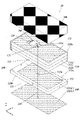
図1は、本開示の第1の実施形態に係るRFIDシステム1を示す図である。
RFIDシステム1は、RFIDタグ10と、当該RFIDタグ10との間で電波を送受信するリーダライタ2とを有する。
このうちRFIDタグ10は、例えば管理対象の物品3の表面に取り付けられて用いられる。また、RFIDタグ10は、電池を内蔵しないタイプであり、リーダライタ2から電磁波を介して電力を受け、この電力によって動作する。なお、RFIDタグ10は、電池を内蔵するタイプであっても良い。(First Embodiment)
FIG. 1 is a diagram showing
The
Of these, the
RFIDタグ10は、RFIDタグ用基板100と、RFIDタグ用基板100の板面に実装されたRFIDタグ用IC(Integrated Circuit)200(半導体集積回路)と、RFIDタグ用基板100のうちRFIDタグ用IC200が実装された板面及びRFIDタグ用IC200を封止する封止部材300と、を備える。
The
RFIDタグ用基板100は、内部に板状逆Fアンテナが形成された直方体形状の板状部材であり、詳細な構成については後述する。
The
RFIDタグ用IC200は、電波の送受信に係る制御を行う制御部と、物品3に関する情報等を記憶する記憶部と、RFIDタグ用基板100のアンテナにそれぞれ電気的に接続される給電端子201(図3参照)及び基準電位端子202(図3参照)と、を有する。RFIDタグ用IC200は、制御部による制御下で、アンテナにより受信された電波に含まれる指令情報を取得し、当該指令情報に応じた処理(例えば、記憶部に記憶される情報の書き換え)を行い、また指令情報により指定された情報を含む電波をアンテナから送信(放射)させる。
The RFID tag IC 200 has a control unit that controls transmission and reception of radio waves, a storage unit that stores information and the like related to the
封止部材300は、RFIDタグ用IC200を覆って保護する。封止部材300は、RFIDタグ用基板100及び封止部材300からなる構造体が全体として直方体形状となるように成形されている。封止部材300としては、例えば、エポキシ樹脂、ポリイミド樹脂およびシリコーン樹脂等を用いることができる。また、これらの樹脂材料にシリカ粒子またはガラス粒子等のフィラー粒子が添加されていても良い。フィラー粒子は、例えば、封止部材300の機械的な強度、耐湿性または電気特性等の各種の特性を調整するために添加される。
The sealing
リーダライタ2は、RFIDタグ10との間で電波を送受信するためのアンテナ2aを有する。リーダライタ2は、RFIDタグ10に対して、情報の書き換えや情報の送信を指令する指令情報を含む電波を送信する。また、リーダライタ2は、指令情報に応じてRFIDタグ10から送信された電波を受信して、当該電波に含まれる情報を取得し、当該情報を用いて所定の処理(例えば、所定の記憶装置への書き込み処理や所定の表示装置における表示処理)を行う。
The reader /
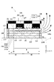
図2A及び図2Bは、RFIDタグ10の構造に応じた電波の放射状態を説明する図である。
RFIDタグには、図2Aに示されるようなキャビティ型のRFIDタグ10Cと、図1や図2Bに示されるような平板型のRFIDタグ10とがある。本実施形態では、平板型のRFIDタグ10が用いられている。
図2A及び図2Bでは、RFIDタグ10C及びRFID10に固定的に定義された直交座標x、y、zが示されている。z方向は、RFIDタグ10C及びRFID10の高さ方向とも呼ぶ。ここで、高さとは、便宜上の呼び方に過ぎず、RFIDタグ10C及びRFID10の使用時における実際の高さ方向(鉛直方向)とは必ずしも一致しない。図3以降の各図に示された直交座標についても同様である。2A and 2B are diagrams illustrating the radiation state of radio waves according to the structure of the
The RFID tag includes a cavity
2A and 2B show Cartesian coordinates x, y, z fixedly defined on
図2Aのキャビティ型のRFIDタグ10Cでは、RFIDタグ用基板100の上面に凹部(キャビティ)が設けられており、凹部の底面にRFIDタグ用IC200が実装され、凹部の内部が封止部材300により封止されている。
一方、図2Bの平板型のRFIDタグ10では、図1で説明したとおり、平板状のRFIDタグ用基板100の上面全体が平板状の封止部材300により封止されている。このような平板型のRFIDタグ10は、RFIDタグ用基板100に凹部を形成する工程が不要であること、また、多数のRFIDタグ用基板100を含む複合基板上の全面に封止部材300を形成した後で分割する方法により効率的に製造することが可能であることなどから、キャビティ型のRFIDタグ10Cに対して製造コストを抑えることが可能である。In the cavity
On the other hand, in the flat plate
キャビティ型のRFIDタグ10C及び平板型のRFIDタグ10のいずれにおいても、RFIDタグ用基板100から送信される電波は、RFIDタグ用基板100の側面(yz平面に平行な面の一方)から放射されて+z方向に回り込むように進行する。物品3におけるRFIDタグ10、10Cの取り付け面から+z方向への電波の送信可能距離は、リーダライタ2から受ける電力の大きさや、RFIDタグ10、10Cのサイズなどにもよるが、通常、数十cm~数m程度である。
In both the cavity
ところで、電波には、より誘電率(比誘電率)が高い物質を通ろうとする性質がある。このため、図2Bの平板型のRFIDタグ10では、RFIDタグ用基板100の側面から外部空間に放射された電波の一部が封止部材300に入射しやすく、電波が所望の方向(+z方向)に放射されにくくなる。他方で、図2Aのキャビティ型のRFIDタグ10Cでは、封止部材300が凹部に埋め込まれているため電波が封止部材300に入射しにくく、このような問題は生じにくい。
このため、RFIDタグ用基板100の構造が(凹部の有無を除いて)共通である場合には、平板型のRFIDタグ10からの電波の+z方向への到達距離L2は、キャビティ型のRFIDタグ10Cからの電波の+z方向への到達距離L1よりも短くなる傾向がある。すなわち、平板型のRFIDタグ10では、キャビティ型のRFIDタグ10Cより通信距離が短くなりやすい。By the way, radio waves have a property of trying to pass through a substance having a higher dielectric constant (relative permittivity). Therefore, in the flat plate
Therefore, when the structure of the
この問題に対し、本実施形態のRFIDタグ10では、平板型の構造を採用して製造コストを抑えつつ、RFIDタグ用基板100の構成を最適化することによって、通信距離をより長くすることが可能となっている。以下では、本実施形態のRFIDタグ10の構成について、RFIDタグ用基板100の構造を中心に説明する。
In response to this problem, in the
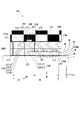
図3は、本実施形態のRFIDタグ10の構成を示す断面図である。
また、図4は、図3のRFIDタグ10の分解斜視図である。
図3及び図4に示されるように、RFIDタグ用基板100は、絶縁基板110と、絶縁基板110の一方の面(+z方向に向いた面。以下では上面110aとも記す)に設けられた上面導体121(第1面導体)、第1の電極124及び第2の電極125と、絶縁基板110の上記一方の面とは反対側の面(-z方向に向いた面。以下では下面110bとも記す)に設けられた下面導体122(第2面導体)と、絶縁基板110の内部に設けられ、下面導体122の一部と対向して下面導体122とともに容量素子140(コンデンサ)を形成する容量導体123と、絶縁基板110を厚さ方向に貫通し、上面導体121と下面導体122とを電気的に接続する短絡部貫通導体131と、絶縁基板110の内部に設けられ、容量導体123と上面導体121とを電気的に接続する容量部貫通導体132と、絶縁基板110の内部に設けられ、第1の電極124と容量導体123とを電気的に接続する層間貫通導体133(第1の層間貫通導体)と、絶縁基板110を厚さ方向に貫通し、第2の電極125と下面導体122とを電気的に接続する層間貫通導体134(第2の層間貫通導体)と、を備える。FIG. 3 is a cross-sectional view showing the configuration of the
Further, FIG. 4 is an exploded perspective view of the
As shown in FIGS. 3 and 4, the
RFIDタグ用基板100は、絶縁基板110の下面110b(下面導体122)が物品3と対向するように物品3に取り付けられて固定される。本実施形態のRFIDタグ10は、物品3の表面が金属等の導体であっても動作する。すなわち、このような物品3に取り付ける場合には、物品3の導体部分がRFIDタグ10のアンテナの接地導体としても機能する。
The
RFIDタグ用IC200は、絶縁基板110の上面に実装されている。また、封止部材300は、絶縁基板110の上面及びRFIDタグ用IC200を覆って封止している。すなわち、絶縁基板110の上面は、RFIDタグ用基板100においてRFIDタグ用IC200が実装され、かつ封止部材300による封止の対象となる、上述の板面を構成する。
The
絶縁基板110は、誘電体(本実施形態では、セラミック)の複数の(ここでは4枚の)積層基板111a~111dが下からこの順に積層された構造を有する板状部材である。絶縁基板110は、xy平面と平行な上面110a及び下面110bを有し、高さ(z方向の長さ)が幅寸(x方向の長さ)及び奥行寸(y方向の長さ)よりも短く、かつ幅寸が奥行寸より長い、x方向に長尺な直方体形状を有する。絶縁基板110を構成する積層基板111a~111dは、例えば、酸化アルミニウム質焼結体、窒化アルミニウム質焼結体、ムライト質焼結体又はガラスセラミック焼結体等の誘電体とすることができる。また、絶縁基板110は、例えばシート状の複数層の(ここでは4層の)セラミックグリーンシートを重ねた上で焼結することで形成することができる。
The insulating
絶縁基板110の上面110aには、+z方向から見て矩形の第1の電極124及び第2の電極125が設けられている。なお、第1の電極124及び第2の電極125の形状は矩形に限られず、他の多角形や円形などであっても良い。
このうち第1の電極124は、RFIDタグ用IC200が有する複数の端子のうち、送信電波に係る電圧信号が出力される給電端子201とボンディングワイヤを介して電気的に接続されている。第1の電極124は、第2の電極125よりも-x方向側に設けられている。
また、第2の電極125は、RFIDタグ用IC200が有する複数の端子のうち、基準電位となる基準電位端子202とボンディングワイヤを介して電気的に接続されている。本実施形態の基準電位は接地電位であり、基準電位端子202は、接地端子である。ただし、基準電位は接地電位に限られず、接地電位以外の所定の電位が基準電位とされても良い。
第1の電極124及び第2の電極125と、RFIDタグ用IC200の端子との接続方法は、ボンディングワイヤを用いたものに限られず、例えばフリップチップ実装により接続されていても良い。The
Among the plurality of terminals of the
Further, the
The method of connecting the
絶縁基板110の上面110aには、上面導体121が設けられている。上面導体121は、x方向に長尺な板状の導体であり、絶縁基板110の上面110aのうち、第1の電極124及び第2の電極125の形成領域を除いたほぼ全面に設けられている。すなわち、上面導体121は、第1の電極124及び第2の電極125の形成領域を確保するための開口部121aを有した形状で設けられている。
下面導体122は、x方向に長尺な板状の導体であり、絶縁基板110の下面110bのほぼ全面に設けられている。An
The
容量導体123は、絶縁基板110のうち最下層の積層基板111aと下から2層目の積層基板111bとの間に設けられた板状の導体であり、下面導体122の一部と対向して容量素子140を形成している。すなわち、容量素子140を形成する一対の導体を第1の導体C1及び第2の導体C2とした場合に、これらのうち+z方向側の第1の導体C1が容量導体123により構成され、-z方向側の第2の導体C2が下面導体122により構成されている。容量導体123には、層間貫通導体134を通過させるための円形の開口部123aが設けられている。開口部123aは、層間貫通導体134から所定距離の間隔(クリアランス)が確保される大きさで形成されている。
The
上面導体121、下面導体122、容量導体123、第1の電極124及び第2の電極125は、積層基板111a~111dがセラミックグリーンシートの段階で、スクリーン印刷等の方法を用いて、金属ペーストをセラミックグリーンシートの該当位置に印刷し、これらを一緒に焼結することで形成することができる。具体的には、まず積層基板111aに対応するセラミックグリーンシートの下面に下面導体122に対応する金属ペーストを印刷し、積層基板111bに対応するセラミックグリーンシートの下面に容量導体123に対応する金属ペーストを印刷する。あるいは、積層基板111aに対応するセラミックグリーンシートの上面に容量導体123に対応する金属ペーストを印刷し、下面に下面導体122に対応する金属ペーストを印刷してもよい。また、積層基板111dに対応するセラミックグリーンシートの上面に、上面導体121、第1の電極124及び第2の電極125に対応する金属ペーストを印刷する。次に、積層基板111a~111dに対応する4層のセラミックグリーンシートを積層した上で、全体を焼結する。これにより、絶縁基板110に、上面導体121、下面導体122、容量導体123、第1の電極124及び第2の電極125を形成することができる。
金属ペーストとしては、例えば、銅の粉末を有機溶剤及び有機バインダと混合した材料が適用できる。上面導体121、下面導体122、第1の電極124及び第2の電極125の露出表面は、ニッケル、コバルト、パラジウム又は金等のめっき層で被覆されてもよく、これにより酸化腐食を抑制することができる。第1の電極124及び第2の電極125については、めっき層の被覆により、ボンディングワイヤとの接合特性も向上する。For the
As the metal paste, for example, a material obtained by mixing copper powder with an organic solvent and an organic binder can be applied. The exposed surfaces of the
短絡部貫通導体131は、絶縁基板110の上面110aと下面110bとの間をz方向に貫通し、上面導体121と下面導体122とを電気的に接続する。短絡部貫通導体131は、絶縁基板110の長手方向(x方向)についての-x方向側の端部に設けられている。よって、短絡部貫通導体131は、上面導体121及び下面導体122の長手方向(x方向)についての-x方向側の端部に接続されている。ここで、絶縁基板110の長手方向についての端部とは、例えば長手方向の一端から、絶縁基板110の長手方向の長さの10%以内の領域とすることができる。短絡部貫通導体131は、x方向及びy方向の幅が、上面導体121及び下面導体122よりも狭く、本実施形態ではピン状とされている。
The short-circuit
容量部貫通導体132は、絶縁基板110のうち上面導体121と容量導体123との間の層に設けられており(すなわち、積層基板111b~111dをz方向に貫通しており)、上面導体121と容量導体123とを電気的に接続する。容量部貫通導体132は、絶縁基板110の長手方向についての+x方向側の端部に設けられている。よって、容量部貫通導体132は、上面導体121及び容量導体123の長手方向についての+x方向側の端部に接続されている。容量部貫通導体132は、短絡部貫通導体131と同様、x方向及びy方向の幅が、上面導体121及び下面導体122よりも狭く、本実施形態ではピン状とされている。
The capacitance
図3及び図4のRFIDタグ10では、短絡部貫通導体131及び容量部貫通導体132が一つずつ設けられているが、図5に示されるように、絶縁基板110の-x方向側の端部に複数の短絡部貫通導体131が設けられ、また絶縁基板110の+x方向側の端部に複数の短絡部貫通導体131が設けられていても良い。また、短絡部貫通導体131及び容量部貫通導体132のうち一方のみが複数設けられていても良い。
In the
層間貫通導体133は、絶縁基板110のうち第1の電極124と容量導体123との間の層に設けられており(すなわち、積層基板111b~111dをz方向に貫通しており)、第1の電極124と容量導体123とを電気的に接続する。層間貫通導体133は、z方向から見て第1の電極124と重なる位置に設けられている。
層間貫通導体134は、絶縁基板110の上面110aと下面110bとの間をz方向に貫通し、第2の電極125と下面導体122とを電気的に接続する。層間貫通導体134は、z方向から見て第2の電極125と重なる位置に設けられている。また、層間貫通導体134は、容量導体123の開口部123aを通るように設けられている。
層間貫通導体133、134は、短絡部貫通導体131と同様、x方向及びy方向の幅が、上面導体121及び下面導体122よりも狭く、本実施形態ではピン状とされている。The interlayer through
The interlayer through
Similar to the short-circuited
短絡部貫通導体131、容量部貫通導体132及び層間貫通導体133、134は、上面導体121等を形成するために金属ペーストを印刷する前の積層基板111a~111dがセラミックグリーンシートの段階で、セラミックグリーンシートに貫通孔又は層間孔を設け、ここに金属ペーストを充填し、これらを一緒に焼結することで形成することができる。金属ペーストとしては、上面導体121の材料と同様、例えば、銅の粉末を有機溶剤及び有機バインダと混合した材料が適用できる。
The short-circuited
このような構成のRFIDタグ用基板100では、上面導体121、下面導体122、容量導体123、短絡部貫通導体131、容量部貫通導体132、層間貫通導体133、134により、板状逆Fアンテナが構成される。このうち上面導体121、容量導体123及び容量部貫通導体132からなる一繋がりの導体は、板状逆Fアンテナの放射導体として作用し、下面導体122は、板状逆Fアンテナの接地導体(地板又は基準電位導体ともいう)として作用する。また、短絡部貫通導体131は、板状逆Fアンテナの電気壁として作用し、層間貫通導体133は、板状逆Fアンテナの給電線として作用し、層間貫通導体134は、板状逆Fアンテナの接地線として作用する。
In the
図3に示されるように、この板状逆Fアンテナでは、主に容量素子140における一対の導体の+x方向側の開口端部140aから電波が放射される。電波は、+x方向側に放射された後、+z方向側に回り込むように進行する。
As shown in FIG. 3, in this plate-shaped inverted-F antenna, radio waves are mainly radiated from the opening
板状逆Fアンテナは、電気的には、電気壁の+x方向側にある放射導体及び短絡導体を、電気壁を対称軸として電気壁の他方側(-x方向側)にも延在させた形状を有するパッチアンテナに相当する。すなわち、放射導体及び短絡導体を電気壁で接続した板状逆Fアンテナの構成によれば、同等の機能を有するパッチアンテナに対して面積を半減させることができる。また、本実施形態の板状逆Fアンテナは、放射導体の一部(容量導体123)と短絡導体(下面導体122)の一部が容量素子140を形成することで波長短縮効果が得られ、これによっても小型化が実現されている。
The plate-shaped inverted-F antenna electrically extends the radial conductor and the short-circuit conductor on the + x direction side of the electric wall to the other side (-x direction side) of the electric wall with the electric wall as the axis of symmetry. It corresponds to a patch antenna having a shape. That is, according to the configuration of the plate-shaped inverted-F antenna in which the radiation conductor and the short-circuit conductor are connected by an electric wall, the area can be halved as compared with the patch antenna having the same function. Further, in the plate-shaped inverted-F antenna of the present embodiment, a wavelength shortening effect can be obtained by forming a
以下では、板状逆Fアンテナの放射導体のうち、第1の電極124との電気的な接続がなされる位置を、接続位置P1と記す。本実施形態では、接続位置P1は、容量導体123と層間貫通導体133とが接続される位置(容量導体123における第1の電極124との電気的な接続位置)である。層間貫通導体133は、第1の電極124から-z方向に延びているため、x方向及びy方向については、接続位置P1は、第1の電極124と同一の位置にある。
また、以下では、板状逆Fアンテナの接地導体のうち、第2の電極125との電気的な接続がなされる位置を、接続位置P2と記す。本実施形態では、接続位置P2は、下面導体122と層間貫通導体134とが接続される位置(下面導体122における第2の電極125との電気的な接続位置)である。層間貫通導体134は、第2の電極125から-z方向に延びているため、x方向及びy方向については、接続位置P2は、第2の電極125と同一の位置にある。In the following, among the radiation conductors of the plate-shaped inverted-F antenna, the position where the electrical connection with the
Further, in the following, among the ground conductors of the plate-shaped inverted-F antenna, the position where the electrical connection with the
本実施形態のRFIDタグ用基板100では、上述のとおり、第1の電極124は、第2の電極125よりも-x方向側に設けられている。したがって、接続位置P1は、接続位置P2よりも-x方向側に位置している。
また、第1の電極124及び第2の電極125が上記の位置関係となっていることにより、第1の電極124と短絡部貫通導体131との距離A1は、第2の電極125と短絡部貫通導体131との距離A2よりも短くなっている。換言すれば、接続位置P1と短絡部貫通導体131との距離A1は、接続位置P2と短絡部貫通導体131との距離A2よりも短くなっている。
また、第1の電極124と容量部貫通導体132との距離B1は、第2の電極125と容量部貫通導体132との距離B2よりも長くなっている。換言すれば、接続位置P1と容量部貫通導体132との距離B1は、接続位置P2と容量部貫通導体132との距離B2よりも長くなっている。In the
Further, since the
Further, the distance B1 between the
RFIDタグ用基板100の板状逆Fアンテナでは、アンテナの動作時に、容量素子140の第1の導体C1(容量導体123)のうち、層間貫通導体133(給電線)との接続位置P1から、容量部貫通導体132との接続位置(以下では、接続位置P3と記す)までの区間Rにおいて主に電流が流れる。このため、この区間Rにおいて、容量素子140の第1の導体C1及び第2の導体C2に、互いに逆極性の電荷が溜まることとなる。なお、図3では、第1の導体C1に正電荷が、また第2の導体C2に負電荷が溜まっている状態が描かれているが、RFIDタグ用IC200の給電端子からは交流の電圧信号が出力されるため、期間によっては、容量素子140に溜まる電荷の極性が図3とは逆になる。
本実施形態のRFIDタグ用基板100では、接続位置P1が接続位置P2より短絡部貫通導体131に近い位置に設けられているため、区間Rをより長く確保することが可能となっている。この構成とする利点について、比較例のRFIDタグ用基板100rの構成と対比して説明する。In the plate-shaped inverted F antenna of the
In the
図6は、比較例のRFIDタグ用基板100rの構成を示す断面図である。
この比較例のRFIDタグ用基板100rでは、第1の電極124及び第2の電極125のx方向についての位置関係が、図3のRFIDタグ用基板100とは逆になっている。よって、層間貫通導体133(給電線)と層間貫通導体134(接地線)のx方向についての位置関係も、図3のRFIDタグ用基板100とは逆になっている。この結果、接続位置P1と短絡部貫通導体131との距離A1が、接続位置P2と短絡部貫通導体131との距離A2よりも長くなっている。また、接続位置P1と容量部貫通導体132との距離B1が、接続位置P2と容量部貫通導体132との距離B2よりも短くなっている。
このような構成の比較例のRFIDタグ用基板100rでは、アンテナの動作時に電流が流れる接続位置P1から接続位置P3までの区間Rが、図3のRFIDタグ用基板100の区間Rよりも短くなる。このため、容量素子140に電荷が溜まりにくくなっている。FIG. 6 is a cross-sectional view showing the configuration of the
In the
In the
これに対し、図3に示される本実施形態のRFIDタグ用基板100では、容量素子140において電荷が溜まる区間Rが、図6の比較例のRFIDタグ用基板100rにおける区間Rより長くなっている。これにより、比較例よりも多くの電荷が容量素子140に溜まり、容量素子140の一対の導体間に生じる電位差をより大きくすることが可能となっている。この結果、板状逆Fアンテナからより強い電波が放出されるため、電波の送信距離、すなわち通信距離をより長くすることができる。
On the other hand, in the
<実施形態の効果>
以上のように、第1の実施形態のRFIDタグ用基板100は、RFIDタグ用ID200が実装される板面を有し、当該板面及びRFIDタグ用ID200が封止部材300により封止されて用いられるRFIDタグ用基板100であって、一方の面が上記板面をなす絶縁基板110と、絶縁基板110の上記一方の面に設けられた上面導体121と、絶縁基板110の上記一方の面とは反対側の面に設けられた下面導体122と、絶縁基板110を厚さ方向に貫通し、上面導体121と下面導体122とを電気的に接続する短絡部貫通導体131と、絶縁基板110の内部に設けられ、下面導体122の少なくとも一部と対向して容量素子140を形成する容量導体123と、絶縁基板110の内部に設けられ、容量導体123と上面導体121とを電気的に接続する容量部貫通導体132と、絶縁基板110の一方の面に設けられ、RFIDタグ用IC200が有する複数の端子のうち送信電波に係る電圧信号が出力される端子が電気的に接続される第1の電極124と、絶縁基板110の一方の面に設けられ、RFIDタグ用IC200が有する複数の端子のうち基準電位となる端子が電気的に接続される第2の電極125と、を備え、容量素子140を形成する一対の導体のうち第1の導体C1(容量導体123)は、短絡部貫通導体131を介さずに第1の電極124に電気的に接続され、一対の導体のうち第2の導体C2(下面導体122)は、短絡部貫通導体131を介さずに第2の電極125に電気的に接続され、第1の電極124から短絡部貫通導体131までの距離A1が、第2の電極125から短絡部貫通導体131までの距離A2より短い。
このような構成によれば、容易に、第1の電極124と容量導体123(放射導体)との接続位置P1を、第2の電極125と下面導体122(接地導体)との接続位置P2よりも短絡部貫通導体131側に設けることができる。すなわち、絶縁基板110の厚さ方向に延びる層間貫通導体133、134で導体間を接続する簡易な構成により、接続位置P1から短絡部貫通導体131までの距離A1を、接続位置P2から短絡部貫通導体131までの距離A2より短くすることができる。
接続位置P1及び接続位置P2がこのような位置関係となることで、容量素子140において電荷が溜まる区間Rを長くすることができる。より具体的には、区間Rの短絡部貫通導体131側の端部位置である接続位置P1を、短絡部貫通導体131側に近付けることで、区間Rを長くすることができる。これによって、より多くの電荷が容量素子140に溜まり、容量素子140の一対の導体間に生じる電位差をより大きくすることができる。この結果、板状逆Fアンテナからより強い電波を放出させることができる。
また、第2の電極125と下面導体122(接地導体)との接続位置P2が、容量素子140の開口端部140aに近い位置となるため、開口端部140aの下面導体122側の電位(基準電位)をより安定させることができる。これによっても、板状逆Fアンテナから放出される電波をより強くすることができる。
このように、本実施形態の構成によれば、板状逆Fアンテナからより強い電波が放出されるため、絶縁基板110の上面110aが封止部材300で封止される構成においても、電波の送信距離、すなわち通信距離をより長くすることができる。<Effect of embodiment>
As described above, the
According to such a configuration, the connection position P1 between the
By having such a positional relationship between the connection position P1 and the connection position P2, it is possible to lengthen the section R in which the electric charge is accumulated in the
Further, since the connection position P2 between the
As described above, according to the configuration of the present embodiment, stronger radio waves are emitted from the plate-shaped inverted-F antenna. Therefore, even in a configuration in which the
また、第1の電極124から容量部貫通導体132までの距離B1が、第2の電極125から容量部貫通導体132までの距離B2より長くなっている。このような構成によれば、容量部貫通導体132と容量導体123との接続位置P3が、第1の電極124と容量導体123との接続位置P1から大きく離れた構成とすることができる。よって、接続位置P1及び接続位置P3を両端とする区間Rを、より長くすることができる。これにより、容量素子140の一対の導体間に生じる電位差をより大きくして、放出される電波の強度をさらに高め、通信距離をより長くすることができる。
Further, the distance B1 from the
また、容量導体123は、下面導体122の少なくとも一部と対向して容量素子140を形成し、容量素子140の第1の導体C1は、容量導体123であり、第2の導体C2は、下面導体122であり、第1の電極124は、絶縁基板110のうち第1の電極124と容量導体123との間の層に設けられた層間貫通導体133を介して容量導体123に電気的に接続され、第2の電極125は、絶縁基板110を貫通する層間貫通導体134を介して下面導体122に電気的に接続され、容量導体123における第1の電極124との電気的な接続位置P1から短絡部貫通導体131までの距離A1が、下面導体122における第2の電極125との電気的な接続位置P2から短絡部貫通導体131までの距離A2より短くなっている。これにより、簡易な層構造で区間Rを長くすることができる。
Further, the
また、容量導体123における第1の電極124との電気的な接続位置P1から容量部貫通導体132までの距離B1が、下面導体122における第2の電極125との電気的な接続位置P2から容量部貫通導体132までの距離B2より長くなっている。これにより、簡易な層構造で区間Rをより長くすることができる。
Further, the distance B1 from the electrical connection position P1 with the
また、上記実施形態のRFIDタグ10は、上記のRFIDタグ用基板100と、RFIDタグ用基板100の板面に実装されたRFIDタグ用IC200と、RFIDタグ用基板100の板面及びRFIDタグ用IC200を封止する封止部材300と、を備える。このような構成によれば、封止部材300により封止がなされていても、通信距離をより長くすることができる。
Further, the
また、上記実施形態のRFIDシステム1は、上記のRFIDタグ10と、RFIDタグ10との間で電波を送受信するリーダライタ2と、を備える。このような構成によれば、RFIDタグ10とリーダライタ2との通信距離の長いRFIDシステム1を実現することができる。
Further, the
(第2の実施形態)
次に、本開示の第2の実施形態について説明する。
本実施形態は、RFIDタグ用基板100の内部構造の一部が第1の実施形態と異なる他は、第1の実施形態と同様である。以下では、第1の実施形態と同一の構成要素については、同一符号を付して、詳細な説明を省略する。(Second embodiment)
Next, a second embodiment of the present disclosure will be described.
This embodiment is the same as the first embodiment except that a part of the internal structure of the
図7は、第2の実施形態のRFIDタグ10の構成を示す断面図である。
また、図8は、図7のRFIDタグ10の分解斜視図である。
図7及び図8に示されるように、本実施形態のRFIDタグ用基板100では、容量導体123が、上面導体121の一部と対向し、上面導体121とともに容量素子140を形成している。すなわち、容量素子140の第1の導体C1が上面導体121により構成されており、第2の導体C2が容量導体123により構成されている。
また、容量部貫通導体132は、絶縁基板110のうち容量導体123と下面導体122との間の層に設けられており(すなわち、積層基板111a~111cをz方向に貫通しており)、容量導体123と下面導体122とを電気的に接続している。
また、第1の電極124は、絶縁基板110の上面110aのうち第1の電極124と上面導体121との間を繋ぐ領域に設けられた接続電極126により、上面導体121と電気的に接続されている。なお、この構成に代えて、第1の電極124と上面導体121とが直接接続された構成や、第1の電極124及び上面導体121が一体的に設けられた構成としても良い。
よって、本実施形態のRFIDタグ用基板100では、上面導体121が板状逆Fアンテナの放射導体を構成し、容量導体123、容量部貫通導体132及び下面導体122が、板状逆Fアンテナの接地導体を構成する。FIG. 7 is a cross-sectional view showing the configuration of the
8 is an exploded perspective view of the
As shown in FIGS. 7 and 8, in the
Further, the capacitance
Further, the
Therefore, in the
したがって、本実施形態では、接続電極126と上面導体121との接続位置が、接続位置P1に相当する。また、層間貫通導体134と下面導体122との接続位置が、接続位置P2に相当する。
本実施形態においても、接続位置P1と短絡部貫通導体131との距離A1は、接続位置P2と短絡部貫通導体131との距離A2よりも短くなっている。また、接続位置P1と容量部貫通導体132との距離B1は、接続位置P2と容量部貫通導体132との距離B2よりも長くなっている。Therefore, in the present embodiment, the connection position between the
Also in this embodiment, the distance A1 between the connection position P1 and the short-circuit portion through
<実施形態の効果>
以上のように、第2の実施形態のRFIDタグ用基板100では、容量導体123は、上面導体121の少なくとも一部と対向して容量素子140を形成している。このような構成によれば、図7に示されるように、容量素子140における一対の導体の開口端部140aの位置(すなわち、板状逆Fアンテナから電波が主に放出される位置)を、封止部材300に近付けることができる。より詳しくは、電波が放出される位置を、封止部材300の直下の位置とすることができる。このような位置から+x方向に放出された電波は、封止部材300との距離が極めて近いため、封止部材300には入射しにくい。これは、電波がその進行方向を旋回させるにはある程度の空間的な広がりが必要なためである(換言すれば、電波は狭い空間で急に曲がることはできないためである)。この結果、放出された電波が封止部材300の影響を受けにくくなるため、通信距離をより長くすることができる。<Effect of embodiment>
As described above, in the
また、第1の導体C1は、上面導体121であり、第2の導体C2は、容量導体123であり、第2の電極125は、絶縁基板110を貫通する第2の層間貫通導体を介して下面導体122に電気的に接続され、上面導体121における第1の電極124との電気的な接続位置P1から短絡部貫通導体131までの距離A1が、下面導体122における第2の電極125との電気的な接続位置P2から短絡部貫通導体131までの距離A2より短くなっている。これにより、簡易な層構成で、容量素子140において電荷が溜まる区間Rを長くすることができる。より具体的には、区間Rの短絡部貫通導体131側の端部位置である接続位置P1を、短絡部貫通導体131側に近付けることで、区間Rを長くすることができる。これにより、容量素子140の一対の導体間に生じる電位差をより大きくして、放出される電波の強度をさらに高め、通信距離をより長くすることができる。
Further, the first conductor C1 is an
また、上面導体121における第1の電極124との電気的な接続位置P1から容量部貫通導体132までの距離B1が、下面導体122における第2の電極125との電気的な接続位置P2から容量部貫通導体132までの距離B2より長くなっている。これにより、容量部貫通導体132と下面導体122との接続位置P3が、第1の電極124と容量導体123との接続位置P1から大きく離れた構成とすることができる。これにより、簡易な層構造で区間Rをより長くすることができる。
Further, the distance B1 from the electrical connection position P1 with the
(第3の実施形態)
次に、本開示の第3の実施形態について説明する。
本実施形態は、第2の電極125と接地導体との接続位置P2が第2の実施形態と異なる他は、第2の実施形態と同様である。以下では、第2の実施形態と同一の構成要素については、同一符号を付して、詳細な説明を省略する。(Third embodiment)
Next, a third embodiment of the present disclosure will be described.
This embodiment is the same as the second embodiment except that the connection position P2 between the
図9は、第3の実施形態のRFIDタグ10の構成を示す断面図である。
また、図10は、図9のRFIDタグ10の分解斜視図である。
図9及び図10に示されるように、本実施形態のRFIDタグ用基板100では、容量導体123が、層間貫通導体135(第3の層間貫通導体)を介して第2の電極125と電気的に接続されている。層間貫通導体135は、絶縁基板110のうち第2の電極125と容量導体123との間の層にのみ設けられている(すなわち、積層基板111dをz方向に貫通している)。また、層間貫通導体135は、z方向から見て第2の電極125と重なる位置に設けられている。FIG. 9 is a cross-sectional view showing the configuration of the
Further, FIG. 10 is an exploded perspective view of the
As shown in FIGS. 9 and 10, in the
よって、本実施形態では、層間貫通導体135と容量導体123との接続位置が、接続位置P2に相当する。また、接続位置P1は、第2の実施形態と同一である。
このような構成の本実施形態においても、接続位置P1と短絡部貫通導体131との距離A1は、接続位置P2と短絡部貫通導体131との距離A2よりも短くなっている。また、接続位置P1と容量部貫通導体132との距離B1は、接続位置P2と容量部貫通導体132との距離B2よりも長くなっている。Therefore, in the present embodiment, the connection position between the interlayer through
Even in the present embodiment having such a configuration, the distance A1 between the connection position P1 and the short-circuit portion through
<実施形態の効果>
以上のように、第3の実施形態のRFIDタグ用基板100では、第1の導体C1は、上面導体121であり、第2の導体C2は、容量導体123であり、第2の電極125は、絶縁基板110のうち第2の電極125と容量導体123との間の層に設けられた第3の層間貫通導体を介して容量導体123に電気的に接続され、上面導体121における第1の電極124との電気的な接続位置P1から短絡部貫通導体131までの距離A1が、容量導体123における第2の電極125との電気的な接続位置P2から短絡部貫通導体131までの距離A2より短くなっている。
このような構成によっても、簡易な層構成で、容量素子140において電荷が溜まる区間Rを長くすることができる。より具体的には、区間Rの短絡部貫通導体131側の端部位置である接続位置P1を、短絡部貫通導体131側に近付けることで、区間Rを長くすることができる。これにより、容量素子140の一対の導体間に生じる電位差をより大きくして、放出される電波の強度をさらに高め、通信距離をより長くすることができる。
さらに、本実施形態の構成では、図9に示されるように、容量素子140と下面導体122との間の領域(以下、容量素子140の「下層領域」と記す)に、第1の電極124又は第2の電極125に電気的に接続された導体が存在しない。よって、第1の電極124と第2の電極125との電位差に応じて下層領域に電荷が溜まりにくいため、下層領域に不要な電界が生じないようにすることができる。また、この結果、容量素子140の第1の導体C1(上面導体121)及び第2の導体C2(容量導体123)に集中的に電荷を蓄積させることができるため、容量素子140の開口端部140aから集中して強い電波を放出することができる。これにより、通信距離をより長くすることができる。<Effect of embodiment>
As described above, in the
Even with such a configuration, it is possible to lengthen the section R in which the electric charge is accumulated in the
Further, in the configuration of the present embodiment, as shown in FIG. 9, the
また、上面導体121における第1の電極124との電気的な接続位置P1から容量部貫通導体132までの距離B1が、容量導体123における第2の電極125との電気的な接続位置P2から容量部貫通導体132までの距離B2より長くなっている。これにより、容量部貫通導体132と下面導体122との接続位置P3が、第1の電極124と容量導体123との接続位置P1から大きく離れた構成とすることができる。よって、簡易な層構造で区間Rをより長くすることができる。
Further, the distance B1 from the electrical connection position P1 with the
また、図3及び図4に示される第1の実施形態のRFIDタグ10と、図9及び図10に示される第3の実施形態のRFIDタグ10と、の各々について、アンテナ利得のシミュレーションを行ったところ、第1の実施形態のRFIDタグ10のアンテナ利得が-26.33dBiとなったのに対し、第3の実施形態のRFIDタグ10のアンテナ利得は-23.78dBiとなり、約2.5dBiの向上が見られた。また、これにより、第3の実施形態の構成における通信距離は、第1の実施形態の構成における通信距離の約1.5倍に改善されることが確認された。これは、図9及び図10のRFIDタグ10では、容量導体123が上面導体121に対向し、容量素子140が封止部材300の直下に設けられていること(すなわち、電波が封止部材300の直下から放射されること)、及び、第2の電極125と接地導体との導通が、第2の電極125と容量導体123との間のみを貫通する層間貫通導体135により行われていることによる効果である。
Further, the antenna gain is simulated for each of the
なお、本開示は、上記実施形態に限られるものではなく、様々な変更が可能である。
例えば、上記実施形態では、容量導体123が、上面導体121の一部、又は下面導体122の一部と対向する例を挙げて説明したが、これに限られず、容量導体123が、上面導体121の全部、又は下面導体122の全部と対向する構成としても良い。The present disclosure is not limited to the above embodiment, and various modifications can be made.
For example, in the above embodiment, the
また、上記実施形態では、RFIDタグ用基板100がx方向に長尺な直方体形状である例を用いて説明したが、これに限られず、z方向から見て正方形となる形状や、y方向に長尺な形状であっても良い。
Further, in the above embodiment, the example in which the
また、絶縁基板110が4層の積層基板111a~111dからなる構成を例に挙げて説明したが、これに限られず、絶縁基板110は、3層以下又は5層以上の積層基板からなるものであっても良い。
Further, the configuration in which the insulating
本開示は、RFIDタグ用基板、RFIDタグ及びRFIDシステムに利用することができる。 The present disclosure can be used for RFID tag substrates, RFID tags and RFID systems.
Claims (11)
一方の面が前記板面をなす絶縁基板と、
前記絶縁基板の前記一方の面に設けられた第1面導体と、
前記絶縁基板の前記一方の面とは反対側の面に設けられた第2面導体と、
前記絶縁基板を厚さ方向に貫通し、前記第1面導体と前記第2面導体とを電気的に接続する短絡部貫通導体と、
前記絶縁基板の内部に設けられ、前記第1面導体の少なくとも一部、又は前記第2面導体の少なくとも一部と対向して容量素子を形成する容量導体と、
前記絶縁基板の内部に設けられ、前記容量導体と、前記第1面導体及び前記第2面導体のうち前記容量導体と対向しない一方と、を電気的に接続する容量部貫通導体と、
前記絶縁基板の前記一方の面に設けられ、前記半導体集積回路が有する複数の端子のうち送信電波に係る電圧信号が出力される端子が電気的に接続される第1の電極と、
前記絶縁基板の前記一方の面に設けられ、前記半導体集積回路が有する複数の端子のうち基準電位となる端子が電気的に接続される第2の電極と、
を備え、
前記容量素子を形成する一対の導体のうち第1の導体は、前記短絡部貫通導体を介さずに前記第1の電極に電気的に接続され、前記一対の導体のうち第2の導体は、前記短絡部貫通導体を介さずに前記第2の電極に電気的に接続され、
前記第1の電極から前記短絡部貫通導体までの距離が、前記第2の電極から前記短絡部貫通導体までの距離より短いRFIDタグ用基板。An RFID tag substrate that has a plate surface on which a semiconductor integrated circuit is mounted, and the plate surface and the semiconductor integrated circuit are sealed by a sealing member.
An insulating substrate whose one surface forms the plate surface,
A first-side conductor provided on one side of the insulating substrate,
A second surface conductor provided on the surface of the insulating substrate opposite to the one surface,
A short-circuited through conductor that penetrates the insulating substrate in the thickness direction and electrically connects the first surface conductor and the second surface conductor.
A capacitive conductor provided inside the insulating substrate and forming a capacitive element facing at least a part of the first surface conductor or at least a part of the second surface conductor.
A capacitive conductor that is provided inside the insulating substrate and electrically connects the capacitive conductor and one of the first-plane conductor and the second-plane conductor that does not face the capacitive conductor.
A first electrode provided on the one surface of the insulating substrate and to which a terminal for outputting a voltage signal related to a transmission radio wave is electrically connected among a plurality of terminals of the semiconductor integrated circuit.
A second electrode provided on the one surface of the insulating substrate and electrically connected to a terminal having a reference potential among a plurality of terminals of the semiconductor integrated circuit.
Equipped with
The first conductor of the pair of conductors forming the capacitive element is electrically connected to the first electrode without passing through the short-circuit portion penetrating conductor, and the second conductor of the pair of conductors is It is electrically connected to the second electrode without passing through the short-circuited through conductor.
An RFID tag substrate in which the distance from the first electrode to the short-circuited through conductor is shorter than the distance from the second electrode to the short-circuited through conductor.
請求項1に記載のRFIDタグ用基板。The distance from the first electrode to the capacitance penetrating conductor is longer than the distance from the second electrode to the capacitance penetrating conductor.
The RFID tag substrate according to claim 1.
前記第1の導体は、前記容量導体であり、前記第2の導体は、前記第2面導体であり、
前記第1の電極は、前記絶縁基板のうち前記第1の電極と前記容量導体との間の層に設けられた第1の層間貫通導体を介して前記容量導体に電気的に接続され、
前記第2の電極は、前記絶縁基板を貫通する第2の層間貫通導体を介して前記第2面導体に電気的に接続され、
前記容量導体における前記第1の電極との電気的な接続位置から前記短絡部貫通導体までの距離が、前記第2面導体における前記第2の電極との電気的な接続位置から前記短絡部貫通導体までの距離より短い、
請求項1又は2に記載のRFIDタグ用基板。The capacitive conductor forms the capacitive element so as to face at least a part of the second surface conductor.
The first conductor is the capacitive conductor, the second conductor is the second surface conductor, and the second conductor is the second surface conductor.
The first electrode is electrically connected to the capacitive conductor via a first interlayer through conductor provided in a layer between the first electrode and the capacitive conductor of the insulating substrate.
The second electrode is electrically connected to the second surface conductor via a second interlayer through conductor penetrating the insulating substrate.
The distance from the electrical connection position with the first electrode in the capacitive conductor to the short-circuited portion penetrating conductor is the short-circuited portion penetrating from the electrical connection position with the second electrode in the second surface conductor. Shorter than the distance to the conductor,
The RFID tag substrate according to claim 1 or 2.
請求項3に記載のRFIDタグ用基板。The distance from the electrical connection position with the first electrode of the capacitive conductor to the capacitive portion penetrating conductor is the distance from the electrical connection position with the second electrode of the second surface conductor to the capacitive portion penetrating conductor. Longer than the distance to the conductor,
The RFID tag substrate according to claim 3.
請求項1又は2に記載のRFIDタグ用基板。 The capacitive conductor forms the capacitive element so as to face at least a part of the first surface conductor.
The RFID tag substrate according to claim 1 or 2.
前記第2の電極は、前記絶縁基板を貫通する第2の層間貫通導体を介して前記第2面導体に電気的に接続され、
前記第1面導体における前記第1の電極との電気的な接続位置から前記短絡部貫通導体までの距離が、前記第2面導体における前記第2の電極との電気的な接続位置から前記短絡部貫通導体までの距離より短い、
請求項5に記載のRFIDタグ用基板。The first conductor is the first surface conductor, and the second conductor is the capacitive conductor.
The second electrode is electrically connected to the second surface conductor via a second interlayer through conductor penetrating the insulating substrate.
The distance from the electrical connection position with the first electrode on the first surface conductor to the short-circuited through conductor is the short circuit from the electrical connection position with the second electrode on the second surface conductor. Shorter than the distance to the part-penetrating conductor,
The RFID tag substrate according to claim 5.
請求項6に記載のRFIDタグ用基板。The distance from the electrical connection position with the first electrode on the first surface conductor to the capacitance portion penetrating conductor is the capacitance from the electrical connection position with the second electrode on the second surface conductor. Longer than the distance to the through-conductor,
The RFID tag substrate according to claim 6.
前記第2の電極は、前記絶縁基板のうち前記第2の電極と前記容量導体との間の層に設けられた第3の層間貫通導体を介して前記容量導体に電気的に接続され、
前記第1面導体における前記第1の電極との電気的な接続位置から前記短絡部貫通導体までの距離が、前記容量導体における前記第2の電極との電気的な接続位置から前記短絡部貫通導体までの距離より短い、
請求項5に記載のRFIDタグ用基板。The first conductor is the first surface conductor, and the second conductor is the capacitive conductor.
The second electrode is electrically connected to the capacitive conductor via a third interlayer through conductor provided in a layer between the second electrode and the capacitive conductor of the insulating substrate.
The distance from the electrical connection position with the first electrode in the first surface conductor to the short-circuited portion penetrating conductor is the short-circuited portion penetrating from the electrical connection position with the second electrode in the capacitive conductor. Shorter than the distance to the conductor,
The RFID tag substrate according to claim 5.
請求項8に記載のRFIDタグ用基板。The distance from the electrical connection position with the first electrode on the first surface conductor to the capacitive portion penetrating conductor is the distance from the electrical connection position with the second electrode on the capacitive conductor to the capacitive portion penetrating conductor. Longer than the distance to the conductor,
The RFID tag substrate according to claim 8.
前記RFIDタグ用基板の前記板面に実装された前記半導体集積回路と、
前記RFIDタグ用基板の前記板面及び前記半導体集積回路を封止する前記封止部材と、
を備えるRFIDタグ。The RFID tag substrate according to any one of claims 1 to 9.
The semiconductor integrated circuit mounted on the plate surface of the RFID tag substrate, and
The sealing member that seals the plate surface of the RFID tag substrate and the semiconductor integrated circuit, and the sealing member.
RFID tag with.
前記RFIDタグとの間で電波を送受信するリーダライタと、
を備えるRFIDシステム。The RFID tag according to claim 10 and
A reader / writer that transmits and receives radio waves to and from the RFID tag,
RFID system with.
Priority Applications (1)
| Application Number | Priority Date | Filing Date | Title |
|---|---|---|---|
| JP2022069140A JP7379580B2 (en) | 2018-08-22 | 2022-04-20 | RFID tag substrate, RFID tag and RFID system |
Applications Claiming Priority (3)
| Application Number | Priority Date | Filing Date | Title |
|---|---|---|---|
| JP2018155087 | 2018-08-22 | ||
| JP2018155087 | 2018-08-22 | ||
| PCT/JP2019/032650 WO2020040202A1 (en) | 2018-08-22 | 2019-08-21 | Rfid tag substrate, rfid tag, and rfid system |
Related Child Applications (1)
| Application Number | Title | Priority Date | Filing Date |
|---|---|---|---|
| JP2022069140A Division JP7379580B2 (en) | 2018-08-22 | 2022-04-20 | RFID tag substrate, RFID tag and RFID system |
Publications (2)
| Publication Number | Publication Date |
|---|---|
| JPWO2020040202A1 JPWO2020040202A1 (en) | 2021-08-26 |
| JP7062772B2 true JP7062772B2 (en) | 2022-05-06 |
Family
ID=69592683
Family Applications (2)
| Application Number | Title | Priority Date | Filing Date |
|---|---|---|---|
| JP2020538437A Active JP7062772B2 (en) | 2018-08-22 | 2019-08-21 | RFID tag boards, RFID tags and RFID systems |
| JP2022069140A Active JP7379580B2 (en) | 2018-08-22 | 2022-04-20 | RFID tag substrate, RFID tag and RFID system |
Family Applications After (1)
| Application Number | Title | Priority Date | Filing Date |
|---|---|---|---|
| JP2022069140A Active JP7379580B2 (en) | 2018-08-22 | 2022-04-20 | RFID tag substrate, RFID tag and RFID system |
Country Status (5)
| Country | Link |
|---|---|
| US (2) | US11354557B2 (en) |
| EP (1) | EP3843009A4 (en) |
| JP (2) | JP7062772B2 (en) |
| CN (1) | CN112602093B (en) |
| WO (1) | WO2020040202A1 (en) |
Families Citing this family (1)
| Publication number | Priority date | Publication date | Assignee | Title |
|---|---|---|---|---|
| CN113015980A (en) * | 2018-11-29 | 2021-06-22 | 京瓷株式会社 | RFID tag |
Citations (3)
| Publication number | Priority date | Publication date | Assignee | Title |
|---|---|---|---|---|
| JP2000101335A (en) | 1998-02-13 | 2000-04-07 | Murata Mfg Co Ltd | Chip antenna, antenna device and mobile communication device |
| WO2018016624A1 (en) | 2016-07-22 | 2018-01-25 | 京セラ株式会社 | Substrate for rfid tags, rfid tag and rfid system |
| WO2018074553A1 (en) | 2016-10-21 | 2018-04-26 | 京セラ株式会社 | Substrate for tags, rfid tag and rfid system |
Family Cites Families (9)
| Publication number | Priority date | Publication date | Assignee | Title |
|---|---|---|---|---|
| US7863718B2 (en) * | 2005-02-16 | 2011-01-04 | Hitachi, Ltd. | Electronic tag chip |
| JP2007124328A (en) * | 2005-10-28 | 2007-05-17 | Shinko Electric Ind Co Ltd | Antenna and wiring board |
| US9064198B2 (en) * | 2006-04-26 | 2015-06-23 | Murata Manufacturing Co., Ltd. | Electromagnetic-coupling-module-attached article |
| US8865298B2 (en) * | 2011-06-29 | 2014-10-21 | Eastman Kodak Company | Article with metal grid composite and methods of preparing |
| US8628840B2 (en) * | 2011-06-29 | 2014-01-14 | Eastman Kodak Company | Electronically conductive laminate donor element |
| WO2013145312A1 (en) | 2012-03-30 | 2013-10-03 | 富士通株式会社 | Rfid tag |
| WO2015132697A1 (en) * | 2014-03-07 | 2015-09-11 | Semiconductor Energy Laboratory Co., Ltd. | Semiconductor device |
| JP6090533B2 (en) * | 2014-05-21 | 2017-03-08 | 株式会社村田製作所 | RFID tag and communication device including the same |
| US10164120B2 (en) * | 2015-05-28 | 2018-12-25 | Semiconductor Energy Laboratory Co., Ltd. | Method for manufacturing semiconductor device |
-
2019
- 2019-08-21 WO PCT/JP2019/032650 patent/WO2020040202A1/en unknown
- 2019-08-21 JP JP2020538437A patent/JP7062772B2/en active Active
- 2019-08-21 US US17/269,051 patent/US11354557B2/en active Active
- 2019-08-21 CN CN201980054128.7A patent/CN112602093B/en active Active
- 2019-08-21 EP EP19851820.1A patent/EP3843009A4/en active Pending
-
2022
- 2022-04-14 US US17/720,973 patent/US11783155B2/en active Active
- 2022-04-20 JP JP2022069140A patent/JP7379580B2/en active Active
Patent Citations (3)
| Publication number | Priority date | Publication date | Assignee | Title |
|---|---|---|---|---|
| JP2000101335A (en) | 1998-02-13 | 2000-04-07 | Murata Mfg Co Ltd | Chip antenna, antenna device and mobile communication device |
| WO2018016624A1 (en) | 2016-07-22 | 2018-01-25 | 京セラ株式会社 | Substrate for rfid tags, rfid tag and rfid system |
| WO2018074553A1 (en) | 2016-10-21 | 2018-04-26 | 京セラ株式会社 | Substrate for tags, rfid tag and rfid system |
Also Published As
| Publication number | Publication date |
|---|---|
| CN112602093B (en) | 2023-07-21 |
| CN112602093A (en) | 2021-04-02 |
| EP3843009A4 (en) | 2022-05-11 |
| US11354557B2 (en) | 2022-06-07 |
| JPWO2020040202A1 (en) | 2021-08-26 |
| JP2022097533A (en) | 2022-06-30 |
| WO2020040202A1 (en) | 2020-02-27 |
| US20210279543A1 (en) | 2021-09-09 |
| US11783155B2 (en) | 2023-10-10 |
| US20220261611A1 (en) | 2022-08-18 |
| JP7379580B2 (en) | 2023-11-14 |
| EP3843009A1 (en) | 2021-06-30 |
Similar Documents
| Publication | Publication Date | Title |
|---|---|---|
| US9705192B2 (en) | Antenna device and communication terminal apparatus | |
| US8336786B2 (en) | Wireless communication device and metal article | |
| CN100514748C (en) | Antenna module and elctronic apparatus having the same | |
| US8981906B2 (en) | Printed wiring board and wireless communication system | |
| CN104051440A (en) | Semiconductor structure having aperture antenna | |
| US10861759B2 (en) | Circuit module | |
| US20180040941A1 (en) | Radio frequency isolator | |
| JP2022097533A (en) | Substrate for rfid tag, rfid tag, and rfid system | |
| JP7142716B2 (en) | RFID tag | |
| JP2019134403A (en) | Chip antenna and chip antenna module including the same | |
| CN111492379B (en) | Substrate for RFID tag, and RFID system | |
| WO2020240895A1 (en) | Rfid tag | |
| JP2020017142A (en) | Cable and electronic device | |
| JP6007750B2 (en) | ANTENNA DEVICE AND COMMUNICATION TERMINAL DEVICE HAVING THE SAME | |
| JP6789172B2 (en) | RFID tag boards, RFID tags and RFID systems | |
| JP2022164692A (en) | Substrate for rfid tag, rfid tag, and rfid system | |
| JPWO2020240895A1 (en) | RFID tag |
Legal Events
| Date | Code | Title | Description |
|---|---|---|---|
| A621 | Written request for application examination |
Free format text: JAPANESE INTERMEDIATE CODE: A621 Effective date: 20210208 |
|
| TRDD | Decision of grant or rejection written | ||
| A01 | Written decision to grant a patent or to grant a registration (utility model) |
Free format text: JAPANESE INTERMEDIATE CODE: A01 Effective date: 20220322 |
|
| A61 | First payment of annual fees (during grant procedure) |
Free format text: JAPANESE INTERMEDIATE CODE: A61 Effective date: 20220420 |
|
| R150 | Certificate of patent or registration of utility model |
Ref document number: 7062772 Country of ref document: JP Free format text: JAPANESE INTERMEDIATE CODE: R150 |