EP3840040A1 - A leadframe for semiconductor devices, corresponding semiconductor product and method - Google Patents
A leadframe for semiconductor devices, corresponding semiconductor product and method Download PDFInfo
- Publication number
- EP3840040A1 EP3840040A1 EP20214010.9A EP20214010A EP3840040A1 EP 3840040 A1 EP3840040 A1 EP 3840040A1 EP 20214010 A EP20214010 A EP 20214010A EP 3840040 A1 EP3840040 A1 EP 3840040A1
- Authority
- EP
- European Patent Office
- Prior art keywords
- leadframe
- die pad
- die
- molding compound
- planar surface
- Prior art date
- Legal status (The legal status is an assumption and is not a legal conclusion. Google has not performed a legal analysis and makes no representation as to the accuracy of the status listed.)
- Granted
Links
Images

Classifications
-
- H—ELECTRICITY
- H10—SEMICONDUCTOR DEVICES; ELECTRIC SOLID-STATE DEVICES NOT OTHERWISE PROVIDED FOR
- H10W—GENERIC PACKAGES, INTERCONNECTIONS, CONNECTORS OR OTHER CONSTRUCTIONAL DETAILS OF DEVICES COVERED BY CLASS H10
- H10W42/00—Arrangements for protection of devices
- H10W42/121—Arrangements for protection of devices protecting against mechanical damage
-
- H—ELECTRICITY
- H10—SEMICONDUCTOR DEVICES; ELECTRIC SOLID-STATE DEVICES NOT OTHERWISE PROVIDED FOR
- H10W—GENERIC PACKAGES, INTERCONNECTIONS, CONNECTORS OR OTHER CONSTRUCTIONAL DETAILS OF DEVICES COVERED BY CLASS H10
- H10W70/00—Package substrates; Interposers; Redistribution layers [RDL]
- H10W70/40—Leadframes
- H10W70/421—Shapes or dispositions
-
- H—ELECTRICITY
- H10—SEMICONDUCTOR DEVICES; ELECTRIC SOLID-STATE DEVICES NOT OTHERWISE PROVIDED FOR
- H10W—GENERIC PACKAGES, INTERCONNECTIONS, CONNECTORS OR OTHER CONSTRUCTIONAL DETAILS OF DEVICES COVERED BY CLASS H10
- H10W70/00—Package substrates; Interposers; Redistribution layers [RDL]
- H10W70/01—Manufacture or treatment
- H10W70/04—Manufacture or treatment of leadframes
-
- H—ELECTRICITY
- H10—SEMICONDUCTOR DEVICES; ELECTRIC SOLID-STATE DEVICES NOT OTHERWISE PROVIDED FOR
- H10W—GENERIC PACKAGES, INTERCONNECTIONS, CONNECTORS OR OTHER CONSTRUCTIONAL DETAILS OF DEVICES COVERED BY CLASS H10
- H10W70/00—Package substrates; Interposers; Redistribution layers [RDL]
- H10W70/01—Manufacture or treatment
- H10W70/04—Manufacture or treatment of leadframes
- H10W70/041—Connecting or disconnecting interconnections to or from leadframes, e.g. connecting bond wires or bumps
-
- H—ELECTRICITY
- H10—SEMICONDUCTOR DEVICES; ELECTRIC SOLID-STATE DEVICES NOT OTHERWISE PROVIDED FOR
- H10W—GENERIC PACKAGES, INTERCONNECTIONS, CONNECTORS OR OTHER CONSTRUCTIONAL DETAILS OF DEVICES COVERED BY CLASS H10
- H10W70/00—Package substrates; Interposers; Redistribution layers [RDL]
- H10W70/01—Manufacture or treatment
- H10W70/04—Manufacture or treatment of leadframes
- H10W70/042—Etching
-
- H—ELECTRICITY
- H10—SEMICONDUCTOR DEVICES; ELECTRIC SOLID-STATE DEVICES NOT OTHERWISE PROVIDED FOR
- H10W—GENERIC PACKAGES, INTERCONNECTIONS, CONNECTORS OR OTHER CONSTRUCTIONAL DETAILS OF DEVICES COVERED BY CLASS H10
- H10W70/00—Package substrates; Interposers; Redistribution layers [RDL]
- H10W70/40—Leadframes
- H10W70/411—Chip-supporting parts, e.g. die pads
-
- H—ELECTRICITY
- H10—SEMICONDUCTOR DEVICES; ELECTRIC SOLID-STATE DEVICES NOT OTHERWISE PROVIDED FOR
- H10W—GENERIC PACKAGES, INTERCONNECTIONS, CONNECTORS OR OTHER CONSTRUCTIONAL DETAILS OF DEVICES COVERED BY CLASS H10
- H10W70/00—Package substrates; Interposers; Redistribution layers [RDL]
- H10W70/40—Leadframes
- H10W70/421—Shapes or dispositions
- H10W70/424—Cross-sectional shapes
-
- H—ELECTRICITY
- H10—SEMICONDUCTOR DEVICES; ELECTRIC SOLID-STATE DEVICES NOT OTHERWISE PROVIDED FOR
- H10W—GENERIC PACKAGES, INTERCONNECTIONS, CONNECTORS OR OTHER CONSTRUCTIONAL DETAILS OF DEVICES COVERED BY CLASS H10
- H10W70/00—Package substrates; Interposers; Redistribution layers [RDL]
- H10W70/40—Leadframes
- H10W70/464—Additional interconnections in combination with leadframes
- H10W70/465—Bumps or wires
-
- H—ELECTRICITY
- H10—SEMICONDUCTOR DEVICES; ELECTRIC SOLID-STATE DEVICES NOT OTHERWISE PROVIDED FOR
- H10W—GENERIC PACKAGES, INTERCONNECTIONS, CONNECTORS OR OTHER CONSTRUCTIONAL DETAILS OF DEVICES COVERED BY CLASS H10
- H10W74/00—Encapsulations, e.g. protective coatings
- H10W74/01—Manufacture or treatment
- H10W74/016—Manufacture or treatment using moulds
-
- H—ELECTRICITY
- H10—SEMICONDUCTOR DEVICES; ELECTRIC SOLID-STATE DEVICES NOT OTHERWISE PROVIDED FOR
- H10W—GENERIC PACKAGES, INTERCONNECTIONS, CONNECTORS OR OTHER CONSTRUCTIONAL DETAILS OF DEVICES COVERED BY CLASS H10
- H10W74/00—Encapsulations, e.g. protective coatings
- H10W74/10—Encapsulations, e.g. protective coatings characterised by their shape or disposition
- H10W74/111—Encapsulations, e.g. protective coatings characterised by their shape or disposition the semiconductor body being completely enclosed
-
- H—ELECTRICITY
- H10—SEMICONDUCTOR DEVICES; ELECTRIC SOLID-STATE DEVICES NOT OTHERWISE PROVIDED FOR
- H10W—GENERIC PACKAGES, INTERCONNECTIONS, CONNECTORS OR OTHER CONSTRUCTIONAL DETAILS OF DEVICES COVERED BY CLASS H10
- H10W74/00—Encapsulations, e.g. protective coatings
- H10W74/10—Encapsulations, e.g. protective coatings characterised by their shape or disposition
- H10W74/111—Encapsulations, e.g. protective coatings characterised by their shape or disposition the semiconductor body being completely enclosed
- H10W74/127—Encapsulations, e.g. protective coatings characterised by their shape or disposition the semiconductor body being completely enclosed characterised by arrangements for sealing or adhesion
-
- H—ELECTRICITY
- H10—SEMICONDUCTOR DEVICES; ELECTRIC SOLID-STATE DEVICES NOT OTHERWISE PROVIDED FOR
- H10W—GENERIC PACKAGES, INTERCONNECTIONS, CONNECTORS OR OTHER CONSTRUCTIONAL DETAILS OF DEVICES COVERED BY CLASS H10
- H10W74/00—Encapsulations, e.g. protective coatings
- H10W74/10—Encapsulations, e.g. protective coatings characterised by their shape or disposition
- H10W74/111—Encapsulations, e.g. protective coatings characterised by their shape or disposition the semiconductor body being completely enclosed
- H10W74/129—Encapsulations, e.g. protective coatings characterised by their shape or disposition the semiconductor body being completely enclosed forming a chip-scale package [CSP]
-
- H—ELECTRICITY
- H10—SEMICONDUCTOR DEVICES; ELECTRIC SOLID-STATE DEVICES NOT OTHERWISE PROVIDED FOR
- H10W—GENERIC PACKAGES, INTERCONNECTIONS, CONNECTORS OR OTHER CONSTRUCTIONAL DETAILS OF DEVICES COVERED BY CLASS H10
- H10W72/00—Interconnections or connectors in packages
- H10W72/50—Bond wires
- H10W72/551—Materials of bond wires
-
- H—ELECTRICITY
- H10—SEMICONDUCTOR DEVICES; ELECTRIC SOLID-STATE DEVICES NOT OTHERWISE PROVIDED FOR
- H10W—GENERIC PACKAGES, INTERCONNECTIONS, CONNECTORS OR OTHER CONSTRUCTIONAL DETAILS OF DEVICES COVERED BY CLASS H10
- H10W72/00—Interconnections or connectors in packages
- H10W72/851—Dispositions of multiple connectors or interconnections
- H10W72/874—On different surfaces
- H10W72/884—Die-attach connectors and bond wires
-
- H—ELECTRICITY
- H10—SEMICONDUCTOR DEVICES; ELECTRIC SOLID-STATE DEVICES NOT OTHERWISE PROVIDED FOR
- H10W—GENERIC PACKAGES, INTERCONNECTIONS, CONNECTORS OR OTHER CONSTRUCTIONAL DETAILS OF DEVICES COVERED BY CLASS H10
- H10W74/00—Encapsulations, e.g. protective coatings
-
- H—ELECTRICITY
- H10—SEMICONDUCTOR DEVICES; ELECTRIC SOLID-STATE DEVICES NOT OTHERWISE PROVIDED FOR
- H10W—GENERIC PACKAGES, INTERCONNECTIONS, CONNECTORS OR OTHER CONSTRUCTIONAL DETAILS OF DEVICES COVERED BY CLASS H10
- H10W90/00—Package configurations
- H10W90/701—Package configurations characterised by the relative positions of pads or connectors relative to package parts
- H10W90/731—Package configurations characterised by the relative positions of pads or connectors relative to package parts of die-attach connectors
- H10W90/736—Package configurations characterised by the relative positions of pads or connectors relative to package parts of die-attach connectors between a chip and a stacked lead frame, conducting package substrate or heat sink
-
- H—ELECTRICITY
- H10—SEMICONDUCTOR DEVICES; ELECTRIC SOLID-STATE DEVICES NOT OTHERWISE PROVIDED FOR
- H10W—GENERIC PACKAGES, INTERCONNECTIONS, CONNECTORS OR OTHER CONSTRUCTIONAL DETAILS OF DEVICES COVERED BY CLASS H10
- H10W90/00—Package configurations
- H10W90/701—Package configurations characterised by the relative positions of pads or connectors relative to package parts
- H10W90/751—Package configurations characterised by the relative positions of pads or connectors relative to package parts of bond wires
- H10W90/756—Package configurations characterised by the relative positions of pads or connectors relative to package parts of bond wires between a chip and a stacked lead frame, conducting package substrate or heat sink
Definitions
- the description relates to integrated circuits (ICs) manufacturing technology.
- One or more embodiments may be applied, in particular, to Quad-Flat No-leads (briefly, QFN) or Quad-Flat Package (QFP) exposed pad semiconductor packaging having exposed leads on the bottom of the package body thereof, and to a method of manufacturing thereof.
- QFN Quad-Flat No-leads
- QFP Quad-Flat Package
- One or more embodiments may be applied to a pre-molded leadframe which is molded in a flat configuration and is adapted for use in package applications using surface mount technology (SMT).
- SMT surface mount technology
- IC dies are conventionally enclosed in plastic packages providing protection from the environment and facilitating electrical interconnection between the IC die and an underlying substrate such as a printed circuit board (PCB).
- PCB printed circuit board
- a packaged semiconductor device may include:
- the leadframe is the central supporting structure for the IC die, in particular during assembly of such a packaged semiconductor device, is adopted to shape external contactors (leads or pads). A portion of the leadframe may be completely surrounded by the plastic encapsulant. Portions of the leads of the leadframe extend externally from the package or are partially exposed within the encapsulant material for use in electrically connecting the package to another component. In certain packaged semiconductor devices, a portion of the die pad of the leadframe may also remain exposed within the exterior of the package for use as a heat sink.
- a QFP package may comprises a thin, generally square package body defining four peripheral sides of substantially equal length. Protruding from each of the four peripheral sides of the package body are a plurality of leads which each have a generally gull-wing configuration. Portions of the leads are internal to the package body, and are electrically connected to respective ones of the pads or terminals of a semiconductor die also encapsulated within the package body.
- the semiconductor die is mounted to a die pad of the QFP package leadframe.
- QFP exposed pad QFP exposed pad
- Package may be stressed during reliability evaluation and the adhesion between all the parts can be ascertained for determining package reliability.
- the leadframe adhesion on the resin is an important figure of merit for the package hermeticity and its reliability.
- QFP package technology external contactors can be shaped by photoetching and, as mentioned, a die pad portion of the leadframe sustaining the IC die silicon chip may be exposed to the exterior of the molded body.
- adhesion/strength is an issue, particularly with pre-molded leadframe and/or when using ribbon bonding (for high-power applications, for instance).
- a molding compound shrinking on a die paddle may result in a compressive stress likely to produce a so-called "crying" warpage leading to resin detachment from leadframe due to lack of adhesion, that is to delamination between the molding compound and the die pad.
- Die pad/molding delamination can jeopardize package hermeticity, as the die pad may be pulled out from the molded body when mounted on PCB.
- An object of one or more embodiments is to contribute in providing improved solutions addressing the issues discussed in the foregoing.
- One or more embodiments facilitate an improved anchorage of the die pad to the molding compound by providing trough slot on die pad periphery, formed by over-lapping of upper and lower half-cut patterns.
- One or more embodiments may relate to a corresponding leadframe.
- a leadframe comprising a die pad having a slot formation on one side and a stepped profile outline may be exemplary of such a leadframe.
- One or more embodiments may relate to a corresponding semiconductor assembly.
- One or more embodiments may relate to a corresponding method.
- a method of manufacturing a leadframe or a semiconductor assembly having improved resilience to delamination may be exemplary of such a method.
- a feature may be included to the die pad area of the leadframe to increase its adhesion to subsequently applied molding compound.
- a feature may comprise a half etch done on an upper side of the die pad, the half etch overlapping partially a second half etch on the bottom of the die pad.
- One or more embodiments may relate to a corresponding leadframe.
- One or more embodiments may create a resin under lock that may facilitate preventing delamination on die pad and increasing die pad hermeticity in the semiconductor assembly.
- such a trough slot perforating partially a half-etched area on die pad periphery may facilitate creating a strong locking by mold compound, preventing a die pad pulling out from the molded body when mounted on a Printed Circuit Board (PCB) .
- PCB Printed Circuit Board
- One or more embodiments may be suited for use in QFN and QFP-ep semiconductor packages with photoetched leadframe.
- the die pad may be designed so as to comprise one or more engraved slots on one surface.
- One or more embodiments may advantageously facilitate, among others:
- improving locking between leadframe and molding compound is an object of one or more embodiments as per the present disclosure.
- some solutions may comprise methods of under-etching the leadframe so as to form an inverted T-shape during an operation of half-cut etching of the leadframe, as exemplified in Figure 1, Figure 2A and Figure 2B .
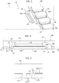
- Figure 1 is a perspective view of a portion of a (metallic, for instance copper) lead-frame 10 subjected to back-etching as discussed in the following, the lead-frame 10 comprising an array of electrical contact formations 16 around a die pad portion.
- a (metallic, for instance copper) lead-frame 10 subjected to back-etching as discussed in the following, the lead-frame 10 comprising an array of electrical contact formations 16 around a die pad portion.
- the array of electrical contact formations 16 may possibly have selectively plated parts provided thereon by known means.
- the leadframe 10 may have a core or die pad area 14 configured to host a semiconductor die.
- the die pad 14 may comprise a first planar die-mounting surface and a second planar surface 14b opposed the first surface.
- the semiconductor die may be glued onto such first surface (not visible in Figure 1 ) and the electrical contact formations 16 may be configured to provide electrical connection and accessibility to the semiconductor die functions once placed on the die pad area 14 of the leadframe 10.
- the die pad 14 may have a polygonal shape, for instance square, and may comprise a generally planar top surface and an opposed, generally planar, bottom surface, as well as four peripheral edge segments.
- a stepped profile 12 may be engraved in the die pad rim or outline as well as in the rim or outline of the leads 16 of the leadframe.
- such a photoetching process may be configured to provide a half-etched leadframe 10 wherein the stepped profile 12 comprises a first step and a second step, the first step having a half-width with respect to the width of the leadframe before etching.
- the leads 16 may be half-etched in a manner facilitating the formation of a continuous, recessed shoulder within the surface thereof, such shoulder extending continuously along the inner end and portions of the longitudinal sides of each lead 16.
- An assembly 100 of the leadframe 10 and a semiconductor die 30 may have a transverse section as exemplified in Figure 2A , wherein the semiconductor die (or dice) may be placed on a first surface 14a of the die pad 14 of the leadframe 10.
- the assembly 100 may be encapsulated or covered with an encapsulant material in a molding process, with the hardening of the encapsulant material resulting in the formation of a package body of the semiconductor package 100.
- the encapsulant material is applied to the leadframe 10 such that in the completely formed package body, the bottom surface 14b of the die pad 14 and the "bottom" surfaces 16b (opposed to respective "top” surfaces 16a) of the electrical contact formations 16 may be exposed within a "bottom” surface of the package assembly 100, wherein the bottom surface of the package assembly 100 may be configured to be coupled to a support S.
- a support S may comprise a Printed Circuit Board, briefly PCB.
- the leadframe 10 may be assembled as a pre-molded leadframe 1000 as exemplified in Figure 2B , for instance having spaces between die pad 14 and leads 16 filled with a molding compound 40', wherein the second surface 14b of the die pad 14 and a top surface 16b of the electrical contact formations 16 may remain visible to external inspection.
- the packaged semiconductor device 100 or pre-molded leadframe 1000 may have an improved resistance to delamination forces which may cause a deterioration of adhesion between molding and leadframe.
- such a resistance may result improved thanks to the presence of the stepped profile outline or recessed shoulder 12 sculptured into the die pad rim, which may counter delamination forces acting parallel to the die pad planar surface 14a.
- such a shoulder 12 may hardly contribute to countering forces acting in other directions, for instance perpendicularly to the die-pad surface. Lack of protection from such (non-parallel) forces may cause in any case a deterioration of adhesion between molding and leadframe: for instance, the leadframe may tend to "slip" outside of its seat as a result of such forces.
- One or more embodiments as per the present disclosure aim at providing such an improved adhesion between leadframe die pad 14 and molding compound 40 with respect to delamination forces acting in any direction.
- such an improvement may be facilitated via a die-pad 14 of a leadframe 20 comprising at least one engraved formation 18, for instance having an oval shape or a mouth portion, going through 18a a first step in a stepped profile 12 outlining the die pad 14.
- the leadframe 20 may be formed from rolled strip metal stock by wet chemical etching or mechanical stamping using progressive dies.
- Photo Chemical etching also known as chemical milling
- Photo Chemical etching is a process that uses photolithography and metal-dissolving chemicals to etch a pattern into a metal strip.
- the photoresist is exposed to ultraviolet light through a photo mask having a desired pattern, and is subsequently developed and cured. Chemicals are sprayed or otherwise applied to the masked strip, and exposed portions of the strip are etched away, leaving the desired pattern.
- the lead frame 20 can be formed by photo-etching or chemically etching the rolled strip metal stock from both sides using a conventional liquid etchant.
- the etch process may be stopped early so as to provide an under-etching of various surfaces of the lead frame 20 to achieve the desired cross-sectional configuration, for instance as exemplified in Figures 2A and/or 2B or in Figure 7 .
- a first mask 70 may be used to etch, for instance with a first etching flow from top 700
- the top surface 14a and a second mask 72 may be used to etch, for instance with a second etching flow from bottom 720, the bottom surface 14b.
- applying such a differentiated etching processing 700, 720 may facilitate obtaining different (engraving) patterns on different leadframe surfaces 14a, 14b.
- Figure 4 is exemplary of a section of one or more embodiments of an assembly 200 of the leadframe 20 and a semiconductor die 30 packaged with an encapsulating molding compound 40.
- the semiconductor die 30 may be coupled to the second surface or "top" surface 14a of the die pad 14 and may be coupled to contact formations 16 via (wire-bonded) contacts 32.
- Figure 5 is an enlarged view of a portion V of Figure 4 .
- the molding compound when poured is coupled to the die pad 14 via an anchoring portion 15 of the die pad 14 which is a result of the engraved formation 18 filled with the molding compound.
- the anchoring 15 may be of various sizes and ratios with respect to the die pad surface 14a as a function of the size of the steps in the rim, for instance of a first step 13 in the stepped profile 12 of the die pad 14.
- the formation 18 may have the shape of an oval slot, such a shape being purely exemplary and in no way limiting.
- the formation 18 may have other polygonal shapes or comprise a pattern of, e.g., parallel, oval or polygonal formations.
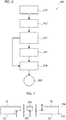
- a method 400 of manufacturing a pre-molded leadframe and/or a semiconductor device as per the present disclosure may comprise:
- the leadframe 20 may be assembled as a pre-molded leadframe by applying, flush to the surface of the leadframe, a molding compound so as to fill spaces between die pad 14, anchoring portion 15 and leads 16 filled with a molding compound 40'.
- the method 400 may comprise providing 420 at least one of a semiconductor device 200 and/or a pre-molded leadframe 2000 having an improved robustness with respect to delamination forces acting in any direction.
- a leadframe for instance, 10 for semiconductor devices which may comprise a die pad portion (for instance, 14) having a first planar die-mounting surface (for instance, 14a) and a second planar surface (for instance, 14b) opposed the first surface, the first surface (for instance, 14a) and the second surface (for instance, 14b) having facing peripheral rims jointly defining a peripheral outline of the die pad, wherein the die pad comprises at least one package molding compound receiving cavity (for instance, 18) opening at the periphery of said first planar surface.
- the peripheral rims said first surface and said second surface may be mutually offset to provide a stepped peripheral outline of the die pad with the periphery of said first planar surface having a peripheral region protruding with respect to the second planar surface, wherein said at least one package molding compound receiving cavity is provided at said protruding region of the first planar surface.
- the at least one package molding compound receiving cavity partially overlaps and goes through said stepped peripheral outline of the die pad.
- said at least one package molding compound receiving cavity may comprise a through cavity (for instance, 18) extending from said first planar surface to said second planar surface.
- said at least one package molding compound receiving cavity may have a mouth portion at said first planar surface, said mouth portion having a closed contour and being at a distance from the peripheral rim of the first planar surface.
- said at least one package molding compound receiving cavity may comprise a buttonhole-like cavity.
- the leadframe may comprise a plurality of said package molding compound receiving cavities (for instance, 15, 18) distributed along the peripheral outline of the die pad.
- the leadframe may have package molding compound (for instance, 40') molded thereon flush with said first planar die-mounting surface and said second planar surface, the package molding compound (for instance, 40) filling said at least one package molding compound receiving cavity opening at the periphery of said first planar surface.
- package molding compound for instance, 40'
- One or more embodiments may relate to a semiconductor product (for instance, 200), comprising:
- the semiconductor product may comprise:
- the method may comprise:
- the method may comprise:
Landscapes
- Lead Frames For Integrated Circuits (AREA)
- Engineering & Computer Science (AREA)
- Microelectronics & Electronic Packaging (AREA)
- Physics & Mathematics (AREA)
- Geometry (AREA)
Abstract
the die pad (14) comprises at least one package molding compound receiving cavity (18) opening at the periphery of said first planar surface (14a),
the peripheral rims of said first surface (14a) and said second surface (14b) are mutually offset to provide a stepped peripheral outline of the die pad (14) with the periphery of said first planar surface (14a) having a peripheral region protruding with respect to the second planar surface (14b), wherein said at least one package molding compound receiving cavity (18) is provided at said protruding region of the first planar surface (14a), and
the at least one package molding compound receiving cavity (18) partially overlaps and goes through said stepped peripheral outline of the die pad (14).
Description
- The description relates to integrated circuits (ICs) manufacturing technology.
- One or more embodiments may be applied, in particular, to Quad-Flat No-leads (briefly, QFN) or Quad-Flat Package (QFP) exposed pad semiconductor packaging having exposed leads on the bottom of the package body thereof, and to a method of manufacturing thereof.
- One or more embodiments may be applied to a pre-molded leadframe which is molded in a flat configuration and is adapted for use in package applications using surface mount technology (SMT).
- IC dies are conventionally enclosed in plastic packages providing protection from the environment and facilitating electrical interconnection between the IC die and an underlying substrate such as a printed circuit board (PCB).
- In a conventional arrangement, a packaged semiconductor device may include:
- a metal leadframe,
- at least one integrated circuit die,
- material to attach the integrated circuit die to a die pad in the leadframe,
- bond wires which electrically connect pads on the IC die to individual leads of the leadframe, and
- a hard plastic encapsulant material, for instance a moulding compound plastic resin, which covers the other components and forms the exterior of the package.
- The leadframe is the central supporting structure for the IC die, in particular during assembly of such a packaged semiconductor device, is adopted to shape external contactors (leads or pads). A portion of the leadframe may be completely surrounded by the plastic encapsulant. Portions of the leads of the leadframe extend externally from the package or are partially exposed within the encapsulant material for use in electrically connecting the package to another component. In certain packaged semiconductor devices, a portion of the die pad of the leadframe may also remain exposed within the exterior of the package for use as a heat sink.
- One type of semiconductor package commonly known in the electronics field is referred to as a quad flat pack (QFP) package. A QFP package may comprises a thin, generally square package body defining four peripheral sides of substantially equal length. Protruding from each of the four peripheral sides of the package body are a plurality of leads which each have a generally gull-wing configuration. Portions of the leads are internal to the package body, and are electrically connected to respective ones of the pads or terminals of a semiconductor die also encapsulated within the package body. The semiconductor die is mounted to a die pad of the QFP package leadframe. In certain types of QFP packages referred to as QFP exposed pad (QFP-ep) packages, one surface of the die pad is exposed within the bottom surface of the package body.
- Package may be stressed during reliability evaluation and the adhesion between all the parts can be ascertained for determining package reliability. The leadframe adhesion on the resin is an important figure of merit for the package hermeticity and its reliability.
- In QFN, QFP package technology external contactors (leads or pads) can be shaped by photoetching and, as mentioned, a die pad portion of the leadframe sustaining the IC die silicon chip may be exposed to the exterior of the molded body.
- In that respect, adhesion/strength is an issue, particularly with pre-molded leadframe and/or when using ribbon bonding (for high-power applications, for instance).
- A molding compound shrinking on a die paddle may result in a compressive stress likely to produce a so-called "crying" warpage leading to resin detachment from leadframe due to lack of adhesion, that is to delamination between the molding compound and the die pad. Die pad/molding delamination can jeopardize package hermeticity, as the die pad may be pulled out from the molded body when mounted on PCB.
- Existing solutions available to leadframe suppliers in order to improve reliability of resin-die pad coupling may comprise surface treatments to the die pad or tailored under (photo) etching of the leadframe.
- Reliability tests performed on such arrangements indicate however that delamination between mold compound and under etch die pad can still take place, with the resulting gap compromising package hermeticity.
- An object of one or more embodiments is to contribute in providing improved solutions addressing the issues discussed in the foregoing.
- According to one or more embodiments, that object can be achieved by means of a system/device/circuit/method having the features set forth in the claims that follow.
- One or more embodiments facilitate an improved anchorage of the die pad to the molding compound by providing trough slot on die pad periphery, formed by over-lapping of upper and lower half-cut patterns.
- One or more embodiments may relate to a corresponding leadframe.
- A leadframe comprising a die pad having a slot formation on one side and a stepped profile outline may be exemplary of such a leadframe.
- One or more embodiments may relate to a corresponding semiconductor assembly.
- One or more embodiments may relate to a corresponding method.
- A method of manufacturing a leadframe or a semiconductor assembly having improved resilience to delamination may be exemplary of such a method.
- In one or more embodiments, may facilitate providing QFP-ep packages with improved package hermeticity and delamination reduced (virtually removed).
- In one or more embodiments, a feature may be included to the die pad area of the leadframe to increase its adhesion to subsequently applied molding compound. Such a feature may comprise a half etch done on an upper side of the die pad, the half etch overlapping partially a second half etch on the bottom of the die pad.
- One or more embodiments may relate to a corresponding leadframe.
- One or more embodiments may create a resin under lock that may facilitate preventing delamination on die pad and increasing die pad hermeticity in the semiconductor assembly.
- In one or more embodiments, such a trough slot perforating partially a half-etched area on die pad periphery may facilitate creating a strong locking by mold compound, preventing a die pad pulling out from the molded body when mounted on a Printed Circuit Board (PCB) .
- One or more embodiments may be suited for use in QFN and QFP-ep semiconductor packages with photoetched leadframe.
- In one or more embodiments, the die pad may be designed so as to comprise one or more engraved slots on one surface.
- One or more embodiments may advantageously facilitate, among others:
- reducing or avoiding delamination between molding compound resin and die pad,
- improving die pad locking in both direction during assembly of a (pre-)molded QFN leadframe,
- providing an alternative to the surface treatments,
- providing an under-etch feature on photoetched lead frames.
- The claims are an integral part of the technical teaching provided herein with reference to the embodiments.
- One or more embodiments will now be described, by way of non-limiting example only, with reference to the annexed Figures, wherein:
-
Figure 1 is a partial perspective view of a leadframe seen from the back or bottom side thereof, -
Figures 2A and 2B are exemplary of possible use of a leadframe as exemplified inFigure 1 , -
Figure 3 is a partial perspective view of a leadframe of one or more embodiments seen from the front or top side thereof, -
Figure 4 is a partial cross-sectional view of a leadframe of one or more embodiments, -
Figure 5 is a view of a portion ofFigure 4 indicated by arrow V reproduced on an enlarged scale and showing possible effects of embodiments, and -
Figure 6 is a flow chart exemplary of possible acts in embodiments, -
Figure 7 is an exemplary diagram of principles underlying embodiments. - In the ensuing description, one or more specific details are illustrated, aimed at providing an in-depth understanding of examples of embodiments of this description. The embodiments may be obtained without one or more of the specific details, or with other methods, components, materials, etc. In other cases, known structures, materials, or operations are not illustrated or described in detail so that certain aspects of embodiments will not be obscured.
- Reference to "an embodiment" or "one embodiment" in the framework of the present description is intended to indicate that a particular configuration, structure, or characteristic described in relation to the embodiment is comprised in at least one embodiment. Hence, phrases such as "in an embodiment" or "in one embodiment" that may be present in one or more points of the present description do not necessarily refer to one and the same embodiment.
- Moreover, particular conformations, structures, or characteristics may be combined in any adequate way in one or more embodiments.
- The references used herein are provided merely for convenience and hence do not define the extent of protection or the scope of the embodiments.
- The drawings are in simplified form and are not to precise scale. For the sake of simplicity, directional (up/down, etc.) or motional (forward/back, etc.) terms may be used with respect to the drawings. The term "couple" and similar terms do not necessarily denote direct and immediate connections, but also include connections through intermediate elements or devices.
- Throughout the figures annexed herein, unless the context indicates otherwise, like parts or elements are indicated with like references/numerals and a corresponding description will not be repeated for brevity.
- As mentioned, improving locking between leadframe and molding compound is an object of one or more embodiments as per the present disclosure.
- In order to facilitate an improved locking, some solutions may comprise methods of under-etching the leadframe so as to form an inverted T-shape during an operation of half-cut etching of the leadframe, as exemplified in
Figure 1, Figure 2A and Figure 2B . -
Figure 1 is a perspective view of a portion of a (metallic, for instance copper) lead-frame 10 subjected to back-etching as discussed in the following, the lead-frame 10 comprising an array ofelectrical contact formations 16 around a die pad portion. - In one or more embodiments, the array of
electrical contact formations 16 may possibly have selectively plated parts provided thereon by known means. - As mentioned, the
leadframe 10 may have a core or diepad area 14 configured to host a semiconductor die. - Specifically, the
die pad 14 may comprise a first planar die-mounting surface and a secondplanar surface 14b opposed the first surface. - For instance, the semiconductor die may be glued onto such first surface (not visible in
Figure 1 ) and theelectrical contact formations 16 may be configured to provide electrical connection and accessibility to the semiconductor die functions once placed on thedie pad area 14 of theleadframe 10. - In one or more embodiments the
die pad 14 may have a polygonal shape, for instance square, and may comprise a generally planar top surface and an opposed, generally planar, bottom surface, as well as four peripheral edge segments. - As a result of the etching processing, for instance, a stepped
profile 12 may be engraved in the die pad rim or outline as well as in the rim or outline of theleads 16 of the leadframe. - Specifically, such a photoetching process may be configured to provide a half-etched
leadframe 10 wherein the steppedprofile 12 comprises a first step and a second step, the first step having a half-width with respect to the width of the leadframe before etching. - As mentioned, during the formation of the
leadframe 10 via etching processing, also theleads 16 may be half-etched in a manner facilitating the formation of a continuous, recessed shoulder within the surface thereof, such shoulder extending continuously along the inner end and portions of the longitudinal sides of each lead 16. - An
assembly 100 of theleadframe 10 and asemiconductor die 30 may have a transverse section as exemplified inFigure 2A , wherein the semiconductor die (or dice) may be placed on afirst surface 14a of thedie pad 14 of theleadframe 10. - Subsequent to the mechanical and electrical connection of the semiconductor die 30 to the
electrical contact formations 16, for instance via through the use of the conductive wires (known as wire bonding, not visible in the Figures), theassembly 100 may be encapsulated or covered with an encapsulant material in a molding process, with the hardening of the encapsulant material resulting in the formation of a package body of thesemiconductor package 100. The encapsulant material is applied to theleadframe 10 such that in the completely formed package body, thebottom surface 14b of thedie pad 14 and the "bottom" surfaces 16b (opposed to respective "top"surfaces 16a) of theelectrical contact formations 16 may be exposed within a "bottom" surface of thepackage assembly 100, wherein the bottom surface of thepackage assembly 100 may be configured to be coupled to a support S. In one or more embodiments, for instance, such a support S may comprise a Printed Circuit Board, briefly PCB. - For instance, the
leadframe 10 may be assembled as apre-molded leadframe 1000 as exemplified inFigure 2B , for instance having spaces betweendie pad 14 and leads 16 filled with a molding compound 40', wherein thesecond surface 14b of thedie pad 14 and atop surface 16b of theelectrical contact formations 16 may remain visible to external inspection. - As mentioned, the packaged
semiconductor device 100 orpre-molded leadframe 1000 may have an improved resistance to delamination forces which may cause a deterioration of adhesion between molding and leadframe. - Specifically, such a resistance may result improved thanks to the presence of the stepped profile outline or recessed
shoulder 12 sculptured into the die pad rim, which may counter delamination forces acting parallel to the die padplanar surface 14a. - Nevertheless, such a
shoulder 12 may hardly contribute to countering forces acting in other directions, for instance perpendicularly to the die-pad surface. Lack of protection from such (non-parallel) forces may cause in any case a deterioration of adhesion between molding and leadframe: for instance, the leadframe may tend to "slip" outside of its seat as a result of such forces. - One or more embodiments as per the present disclosure aim at providing such an improved adhesion between leadframe die
pad 14 andmolding compound 40 with respect to delamination forces acting in any direction. - In one or more embodiments as exemplified in
Figure 3 such an improvement may be facilitated via a die-pad 14 of aleadframe 20 comprising at least oneengraved formation 18, for instance having an oval shape or a mouth portion, going through 18a a first step in a steppedprofile 12 outlining thedie pad 14. - The
leadframe 20 may be formed from rolled strip metal stock by wet chemical etching or mechanical stamping using progressive dies. Photo Chemical etching (also known as chemical milling) is a process that uses photolithography and metal-dissolving chemicals to etch a pattern into a metal strip. The photoresist is exposed to ultraviolet light through a photo mask having a desired pattern, and is subsequently developed and cured. Chemicals are sprayed or otherwise applied to the masked strip, and exposed portions of the strip are etched away, leaving the desired pattern. - As mentioned, the
lead frame 20 can be formed by photo-etching or chemically etching the rolled strip metal stock from both sides using a conventional liquid etchant. The etch process may be stopped early so as to provide an under-etching of various surfaces of thelead frame 20 to achieve the desired cross-sectional configuration, for instance as exemplified inFigures 2A and/or 2B or inFigure 7 . - Specifically, in one or more embodiments as exemplified in
Figure 7 , different masked strips may be used for different sides of the leadframe. For instance, afirst mask 70 may be used to etch, for instance with a first etching flow from top 700, thetop surface 14a and asecond mask 72 may be used to etch, for instance with a second etching flow frombottom 720, thebottom surface 14b. In one or more embodiments, applying such adifferentiated etching processing different leadframe surfaces Figure 4 is exemplary of a section of one or more embodiments of anassembly 200 of theleadframe 20 and asemiconductor die 30 packaged with an encapsulatingmolding compound 40. - For instance, the semiconductor die 30 may be coupled to the second surface or "top"
surface 14a of thedie pad 14 and may be coupled to contactformations 16 via (wire-bonded)contacts 32.Figure 5 is an enlarged view of a portion V ofFigure 4 . In one or more embodiments as exemplified inFigure 5 , thanks to the presence offormation 18 which goes through the steppedprofile 12 of thedie pad 14, the molding compound when poured is coupled to thedie pad 14 via an anchoringportion 15 of thedie pad 14 which is a result of the engravedformation 18 filled with the molding compound. The anchoring 15 may be of various sizes and ratios with respect to thedie pad surface 14a as a function of the size of the steps in the rim, for instance of afirst step 13 in the steppedprofile 12 of thedie pad 14. - In one or more embodiments as exemplified in
Figure 3 , theformation 18 may have the shape of an oval slot, such a shape being purely exemplary and in no way limiting. For instance, theformation 18 may have other polygonal shapes or comprise a pattern of, e.g., parallel, oval or polygonal formations. - In one or more embodiments as exemplified in
Figure 6 , amethod 400 of manufacturing a pre-molded leadframe and/or a semiconductor device as per the present disclosure may comprise: - providing 410 a (metallic, for instance copper) leadframe, the
leadframe 10 comprising adie pad 14 and a plurality ofleads 16, - applying under-
etching 412, e.g. photo etching or chemical etching, to afirst side leadframe 10, so as to impart a step profile to the outline of thedie pad 14 and, mirror symmetrically, the outline of leads in the plurality ofleads 16, the stepped profile comprising a first step and a second step; - applying
etching processing 414, e.g. photo or chemical etching, to asecond side second surface 14a of thedie pad area 14 in the leadframe so as to etch at least one formation and/or a pattern of formations, going through the first step in the steppedprofile 12 outlining thedie pad 14; - coupling 414 a semiconductor die to the second
die pad surface 14a of thedie pad 14; - electrically coupling 416 the semiconductor die 30 to the
electrical contact formations 16 in the leadframe, for instance viawire bonding 32, and - applying a
molding compound 418 filling a volume comprising at least saidleadframe 10 and in a way so that a seconddie pad surface 14b opposed said firstdie pad surface 14a of the die pad is exposed to the outside and wherein the at least oneformation 18 etched in thedie pad 14 is filled with saidmolding compound 40. - For instance, the
leadframe 20 may be assembled as a pre-molded leadframe by applying, flush to the surface of the leadframe, a molding compound so as to fill spaces betweendie pad 14, anchoringportion 15 and leads 16 filled with a molding compound 40'. - As a result, the
method 400 may comprise providing 420 at least one of asemiconductor device 200 and/or a pre-molded leadframe 2000 having an improved robustness with respect to delamination forces acting in any direction. - One or more embodiments relate to a leadframe (for instance, 10) for semiconductor devices which may comprise a die pad portion (for instance, 14) having a first planar die-mounting surface (for instance, 14a) and a second planar surface (for instance, 14b) opposed the first surface, the first surface (for instance, 14a) and the second surface (for instance, 14b) having facing peripheral rims jointly defining a peripheral outline of the die pad, wherein the die pad comprises at least one package molding compound receiving cavity (for instance, 18) opening at the periphery of said first planar surface.
- In one or more embodiments, the peripheral rims said first surface and said second surface may be mutually offset to provide a stepped peripheral outline of the die pad with the periphery of said first planar surface having a peripheral region protruding with respect to the second planar surface, wherein said at least one package molding compound receiving cavity is provided at said protruding region of the first planar surface.
- In one or more embodiments, the at least one package molding compound receiving cavity partially overlaps and goes through said stepped peripheral outline of the die pad.
- In one or more embodiments, said at least one package molding compound receiving cavity may comprise a through cavity (for instance, 18) extending from said first planar surface to said second planar surface.
- In one or more embodiments, said at least one package molding compound receiving cavity may have a mouth portion at said first planar surface, said mouth portion having a closed contour and being at a distance from the peripheral rim of the first planar surface.
- In one or more embodiments, said at least one package molding compound receiving cavity may comprise a buttonhole-like cavity.
- In one or more embodiments, the leadframe may comprise a plurality of said package molding compound receiving cavities (for instance, 15, 18) distributed along the peripheral outline of the die pad.
- In one or more embodiments, the leadframe may have package molding compound (for instance, 40') molded thereon flush with said first planar die-mounting surface and said second planar surface, the package molding compound (for instance, 40) filling said at least one package molding compound receiving cavity opening at the periphery of said first planar surface.
- One or more embodiments may relate to a semiconductor product (for instance, 200), comprising:
- a leadframe (for instance, 10) according to one or more embodiments,
- at least one semiconductor die (for instance, 30) coupled to said first planar surface (for instance, 14a) in the die pad (for instance, 14) of the leadframe.
- In one or more embodiments, the semiconductor product may comprise:
- electrically-conductive formations (for instance, 32) electrically coupling said at least one semiconductor die with said leadframe and/or
- package molding compound (for instance, 40) encapsulating said at least one semiconductor die coupled to said first planar surface in the die pad of the leadframe.
- One or more embodiments may relate to a method which may comprise:
- providing (for instance, 410) a leadframe (for instance, 10) for semiconductor devices, the leadframe comprising a die pad portion (for instance, 14) having a first planar die-mounting surface (for instance, 14a) and a second planar surface (for instance, 14b) opposed the first surface,
- applying etching processing (for instance, 412), preferably photo-etching processing, to said first surface and said second surface, the first surface and the second surface having facing peripheral rims jointly defining a peripheral outline of the die pad, wherein the die pad comprises at least one package molding compound receiving cavity (for instance, 15, 18) opening at the periphery of said first planar surface.
- In one or more embodiments, the method may comprise:
- coupling (for instance, 414) at least one semiconductor die (for instance, 30) to said first planar surface in the die pad of the leadframe.
- In one or more embodiments, the method may comprise:
- electrically coupling said at least one semiconductor die with said leadframe, and/or
- encapsulating (for instance, 40) said at least one semiconductor die coupled to said first planar surface in the die pad of the leadframe.
- It will be otherwise understood that the various individual implementing options exemplified throughout the figures accompanying this description are not necessarily intended to be adopted in the same combinations exemplified in the figures. One or more embodiments may thus adopt these (otherwise non-mandatory) options individually and/or in different combinations with respect to the combination exemplified in the accompanying figures.
- Without prejudice to the underlying principles, the details and embodiments may vary, even significantly, with respect to what has been described by way of example only, without departing from the extent of protection. The extent of protection is defined by the annexed claims.
Claims (11)
- A leadframe (10) for semiconductor devices, the leadframe (10) comprising a die pad portion (14) having a first planar die-mounting surface (14a) and a second planar surface (14b) opposed the first surface (14a), the first surface (14a) and the second surface (14b) having facing peripheral rims jointly defining a peripheral outline of the die pad (14), wherein:the die pad (14) comprises at least one package molding compound receiving cavity (18) opening at the periphery of said first planar surface (14a),the peripheral rims of said first surface (14a) and said second surface (14b) are mutually offset to provide a stepped peripheral outline of the die pad (14) with the periphery of said first planar surface (14a) having a peripheral region protruding with respect to the second planar surface (14b), wherein said at least one package molding compound receiving cavity (18) is provided at said protruding region of the first planar surface (14a), andthe at least one package molding compound receiving cavity (18) partially overlaps and goes through said stepped peripheral outline of the die pad (14).
- The leadframe of claim 1 having package molding compound (40') molded thereon flush with said first planar die-mounting surface (14a) and said second planar surface (14b), the package molding compound (40) filling said at least one package molding compound receiving cavity (18) opening at the periphery of said first planar surface (14a).
- The leadframe (10) of claim 1 or claim 2, wherein said at least one package molding compound receiving cavity (18) comprises a through cavity (18a) extending from said first planar surface (14a) to said second planar surface (14b).
- The leadframe (10) of any of the previous claims, wherein said at least one package molding compound receiving cavity (18) has a mouth portion at said first planar surface (14a), said mouth portion having a closed contour and being at a distance from the peripheral rim of the first planar surface (14a).
- The leadframe (10) of any of the previous claims, wherein said at least one package molding compound receiving cavity (18) comprises a buttonhole-like cavity.
- The leadframe (10) of any of the previous claims, comprising a plurality of said package molding compound receiving cavities (18) distributed along the peripheral outline of the die pad (14).
- A semiconductor product (200), comprising:a leadframe (10) according to any of claims 1 to 6,at least one semiconductor die (30) coupled to said first planar surface (14a) in the die pad (14) of the leadframe (10).
- The semiconductor product of claim 7, comprising:electrically-conductive formations (32) electrically coupling said at least one semiconductor die (30) with said leadframe (10) and/orpackage molding compound (40) encapsulating said at least one semiconductor die (30) coupled to said first planar surface (14a) in the die pad (14) of the leadframe (10) .
- A method, comprising:- providing (410) a leadframe (10) for semiconductor devices, the leadframe (10) comprising a die pad portion (14) having a first planar die-mounting surface (14a) and a second planar surface (14b) opposed the first surface (14a),- applying etching processing (412), preferably photo-etching processing, to said first surface (14a) and said second surface (14b), the first surface (14a) and the second surface (14b) having facing peripheral rims jointly defining a peripheral outline of the die pad (14), wherein the die pad (14) comprises at least one package molding compound receiving cavity (15) opening at the periphery of said first planar surface (14a) .
- The method of claim 9, comprising:- coupling (414) at least one semiconductor die (30) to said first planar surface (14a) in the die pad (14) of the leadframe (10).
- The method of claim 9 or claim 10, comprising:- electrically coupling said at least one semiconductor die (30) with said leadframe (10), and/or- encapsulating (40) said at least one semiconductor die (30) coupled to said first planar surface (14a) in the die pad (14) of the leadframe (10).
Applications Claiming Priority (1)
| Application Number | Priority Date | Filing Date | Title |
|---|---|---|---|
| IT102019000025009A IT201900025009A1 (en) | 2019-12-20 | 2019-12-20 | LEADFRAME FOR SEMICONDUCTOR DEVICES, SEMICONDUCTOR PRODUCT AND CORRESPONDING PROCEDURE |
Publications (2)
| Publication Number | Publication Date |
|---|---|
| EP3840040A1 true EP3840040A1 (en) | 2021-06-23 |
| EP3840040B1 EP3840040B1 (en) | 2025-05-14 |
Family
ID=69904132
Family Applications (1)
| Application Number | Title | Priority Date | Filing Date |
|---|---|---|---|
| EP20214010.9A Active EP3840040B1 (en) | 2019-12-20 | 2020-12-15 | A leadframe for semiconductor devices, corresponding semiconductor product and method |
Country Status (4)
| Country | Link |
|---|---|
| US (1) | US11557547B2 (en) |
| EP (1) | EP3840040B1 (en) |
| CN (2) | CN113013127B (en) |
| IT (1) | IT201900025009A1 (en) |
Cited By (1)
| Publication number | Priority date | Publication date | Assignee | Title |
|---|---|---|---|---|
| IT202100020114A1 (en) | 2021-07-28 | 2023-01-28 | St Microelectronics Srl | Method of manufacturing substrates for semiconductor devices, the corresponding substrate and semiconductor device |
Families Citing this family (1)
| Publication number | Priority date | Publication date | Assignee | Title |
|---|---|---|---|---|
| IT201900025009A1 (en) * | 2019-12-20 | 2021-06-20 | St Microelectronics Srl | LEADFRAME FOR SEMICONDUCTOR DEVICES, SEMICONDUCTOR PRODUCT AND CORRESPONDING PROCEDURE |
Citations (6)
| Publication number | Priority date | Publication date | Assignee | Title |
|---|---|---|---|---|
| JP2001044351A (en) * | 1999-07-29 | 2001-02-16 | Hitachi Ltd | Semiconductor device and method of manufacturing the same |
| US20020117740A1 (en) * | 2001-02-28 | 2002-08-29 | Advanced Semiconductor Engineering Inc. | Lead frame for plastic molded type semiconductor package |
| US20050199986A1 (en) * | 2004-03-11 | 2005-09-15 | Advanced Semiconductor Engineering, Inc. | Leadframe with die pad |
| US20070052070A1 (en) * | 2005-09-06 | 2007-03-08 | Shafidul Islam | Die pad for semiconductor packages and methods of making and using same |
| US20070111379A1 (en) * | 2005-10-21 | 2007-05-17 | Stats Chippac Ltd. | Pre-molded leadframe and method therefor |
| US20170033056A1 (en) * | 2007-01-30 | 2017-02-02 | Rohm Co., Ltd. | Resin-encapsulated semiconductor device and its manufacturing method |
Family Cites Families (10)
| Publication number | Priority date | Publication date | Assignee | Title |
|---|---|---|---|---|
| JPH01278757A (en) * | 1988-05-02 | 1989-11-09 | Matsushita Electron Corp | Lead frame |
| JPH043450A (en) * | 1990-04-19 | 1992-01-08 | Mitsubishi Electric Corp | Resin sealed semiconductor device |
| KR200292411Y1 (en) * | 1997-11-21 | 2002-12-18 | 주식회사 하이닉스반도체 | Leadframe for Small Die Pad Package |
| JP4417541B2 (en) * | 2000-10-23 | 2010-02-17 | ローム株式会社 | Semiconductor device and manufacturing method thereof |
| US7732914B1 (en) | 2002-09-03 | 2010-06-08 | Mclellan Neil | Cavity-type integrated circuit package |
| JP2006318996A (en) * | 2005-05-10 | 2006-11-24 | Matsushita Electric Ind Co Ltd | Lead frame and resin-encapsulated semiconductor device |
| CN101697348B (en) * | 2009-10-11 | 2013-06-26 | 天水华天科技股份有限公司 | Small-carrier flat-four-side pin-less packaging part and preparation method thereof |
| US8604596B2 (en) * | 2011-03-24 | 2013-12-10 | Stats Chippac Ltd. | Integrated circuit packaging system with locking interconnects and method of manufacture thereof |
| US20200135632A1 (en) | 2018-10-24 | 2020-04-30 | Texas Instruments Incorporated | Die isolation on a substrate |
| IT201900025009A1 (en) * | 2019-12-20 | 2021-06-20 | St Microelectronics Srl | LEADFRAME FOR SEMICONDUCTOR DEVICES, SEMICONDUCTOR PRODUCT AND CORRESPONDING PROCEDURE |
-
2019
- 2019-12-20 IT IT102019000025009A patent/IT201900025009A1/en unknown
-
2020
- 2020-12-15 EP EP20214010.9A patent/EP3840040B1/en active Active
- 2020-12-18 US US17/126,880 patent/US11557547B2/en active Active
- 2020-12-21 CN CN202011518461.XA patent/CN113013127B/en active Active
- 2020-12-21 CN CN202023092967.7U patent/CN214505480U/en not_active Withdrawn - After Issue
Patent Citations (6)
| Publication number | Priority date | Publication date | Assignee | Title |
|---|---|---|---|---|
| JP2001044351A (en) * | 1999-07-29 | 2001-02-16 | Hitachi Ltd | Semiconductor device and method of manufacturing the same |
| US20020117740A1 (en) * | 2001-02-28 | 2002-08-29 | Advanced Semiconductor Engineering Inc. | Lead frame for plastic molded type semiconductor package |
| US20050199986A1 (en) * | 2004-03-11 | 2005-09-15 | Advanced Semiconductor Engineering, Inc. | Leadframe with die pad |
| US20070052070A1 (en) * | 2005-09-06 | 2007-03-08 | Shafidul Islam | Die pad for semiconductor packages and methods of making and using same |
| US20070111379A1 (en) * | 2005-10-21 | 2007-05-17 | Stats Chippac Ltd. | Pre-molded leadframe and method therefor |
| US20170033056A1 (en) * | 2007-01-30 | 2017-02-02 | Rohm Co., Ltd. | Resin-encapsulated semiconductor device and its manufacturing method |
Cited By (2)
| Publication number | Priority date | Publication date | Assignee | Title |
|---|---|---|---|---|
| IT202100020114A1 (en) | 2021-07-28 | 2023-01-28 | St Microelectronics Srl | Method of manufacturing substrates for semiconductor devices, the corresponding substrate and semiconductor device |
| EP4125121A1 (en) | 2021-07-28 | 2023-02-01 | STMicroelectronics S.r.l. | Method of manufacturing substrates for semiconductor devices, corresponding substrate and semiconductor device |
Also Published As
| Publication number | Publication date |
|---|---|
| CN113013127A (en) | 2021-06-22 |
| IT201900025009A1 (en) | 2021-06-20 |
| CN214505480U (en) | 2021-10-26 |
| US11557547B2 (en) | 2023-01-17 |
| EP3840040B1 (en) | 2025-05-14 |
| CN113013127B (en) | 2026-01-30 |
| US20210193591A1 (en) | 2021-06-24 |
Similar Documents
| Publication | Publication Date | Title |
|---|---|---|
| CN100533722C (en) | Semiconductor device | |
| CN101656234B (en) | Advanced quad flat non-leaded package structure and manufacturing method thereof | |
| CN100490140C (en) | Double gauge lead frame | |
| US20080283980A1 (en) | Lead frame for semiconductor package | |
| US20030073265A1 (en) | Semiconductor package with singulation crease | |
| US20050218499A1 (en) | Method for manufacturing leadless semiconductor packages | |
| WO2002020236A2 (en) | A mold | |
| US20180122731A1 (en) | Plated ditch pre-mold lead frame, semiconductor package, and method of making same | |
| CN101587879A (en) | Lead frame and resin-encapsulated semiconductor device | |
| US6882048B2 (en) | Lead frame and semiconductor package having a groove formed in the respective terminals for limiting a plating area | |
| EP3840040B1 (en) | A leadframe for semiconductor devices, corresponding semiconductor product and method | |
| US6703694B2 (en) | Frame for semiconductor package including plural lead frames having thin parts or hollows adjacent the terminal roots | |
| US20060199308A1 (en) | Process for manufacturing sawing type leadless semiconductor packages | |
| KR20040108582A (en) | Seniconductor device and method for fabricating the same | |
| US6921967B2 (en) | Reinforced die pad support structure | |
| US20240297147A1 (en) | Hybrid multi-die qfp-qfn package | |
| US20070077732A1 (en) | Semiconductor device and a manufacturing method of the same | |
| US7498665B2 (en) | Integrated circuit leadless package system | |
| CN212209475U (en) | Lead frame and package | |
| EP4016617A1 (en) | Method of manufacturing semiconductor devices, component for use therein and corresponding semiconductor device | |
| JP4475785B2 (en) | Manufacturing method of resin-encapsulated semiconductor device | |
| US20030098503A1 (en) | Frame for semiconductor package | |
| US12400939B2 (en) | Packaged semiconductor device including heat slug | |
| JP3687347B2 (en) | Resin-sealed semiconductor device | |
| JP4356960B2 (en) | Resin-sealed semiconductor device |
Legal Events
| Date | Code | Title | Description |
|---|---|---|---|
| PUAI | Public reference made under article 153(3) epc to a published international application that has entered the european phase |
Free format text: ORIGINAL CODE: 0009012 |
|
| STAA | Information on the status of an ep patent application or granted ep patent |
Free format text: STATUS: THE APPLICATION HAS BEEN PUBLISHED |
|
| AK | Designated contracting states |
Kind code of ref document: A1 Designated state(s): AL AT BE BG CH CY CZ DE DK EE ES FI FR GB GR HR HU IE IS IT LI LT LU LV MC MK MT NL NO PL PT RO RS SE SI SK SM TR |
|
| STAA | Information on the status of an ep patent application or granted ep patent |
Free format text: STATUS: REQUEST FOR EXAMINATION WAS MADE |
|
| 17P | Request for examination filed |
Effective date: 20211129 |
|
| RBV | Designated contracting states (corrected) |
Designated state(s): AL AT BE BG CH CY CZ DE DK EE ES FI FR GB GR HR HU IE IS IT LI LT LU LV MC MK MT NL NO PL PT RO RS SE SI SK SM TR |
|
| GRAP | Despatch of communication of intention to grant a patent |
Free format text: ORIGINAL CODE: EPIDOSNIGR1 |
|
| STAA | Information on the status of an ep patent application or granted ep patent |
Free format text: STATUS: GRANT OF PATENT IS INTENDED |
|
| INTG | Intention to grant announced |
Effective date: 20250109 |
|
| RIN1 | Information on inventor provided before grant (corrected) |
Inventor name: MAZZOLA, MAURO Inventor name: TIZIANI, ROBERTO |
|
| GRAS | Grant fee paid |
Free format text: ORIGINAL CODE: EPIDOSNIGR3 |
|
| GRAA | (expected) grant |
Free format text: ORIGINAL CODE: 0009210 |
|
| STAA | Information on the status of an ep patent application or granted ep patent |
Free format text: STATUS: THE PATENT HAS BEEN GRANTED |
|
| AK | Designated contracting states |
Kind code of ref document: B1 Designated state(s): AL AT BE BG CH CY CZ DE DK EE ES FI FR GB GR HR HU IE IS IT LI LT LU LV MC MK MT NL NO PL PT RO RS SE SI SK SM TR |
|
| REG | Reference to a national code |
Ref country code: GB Ref legal event code: FG4D |
|
| REG | Reference to a national code |
Ref country code: CH Ref legal event code: EP |
|
| REG | Reference to a national code |
Ref country code: IE Ref legal event code: FG4D |
|
| REG | Reference to a national code |
Ref country code: DE Ref legal event code: R096 Ref document number: 602020051197 Country of ref document: DE |
|
| REG | Reference to a national code |
Ref country code: NL Ref legal event code: MP Effective date: 20250514 |
|
| PG25 | Lapsed in a contracting state [announced via postgrant information from national office to epo] |
Ref country code: PT Free format text: LAPSE BECAUSE OF FAILURE TO SUBMIT A TRANSLATION OF THE DESCRIPTION OR TO PAY THE FEE WITHIN THE PRESCRIBED TIME-LIMIT Effective date: 20250915 Ref country code: FI Free format text: LAPSE BECAUSE OF FAILURE TO SUBMIT A TRANSLATION OF THE DESCRIPTION OR TO PAY THE FEE WITHIN THE PRESCRIBED TIME-LIMIT Effective date: 20250514 Ref country code: ES Free format text: LAPSE BECAUSE OF FAILURE TO SUBMIT A TRANSLATION OF THE DESCRIPTION OR TO PAY THE FEE WITHIN THE PRESCRIBED TIME-LIMIT Effective date: 20250514 |
|
| REG | Reference to a national code |
Ref country code: LT Ref legal event code: MG9D |
|
| PG25 | Lapsed in a contracting state [announced via postgrant information from national office to epo] |
Ref country code: GR Free format text: LAPSE BECAUSE OF FAILURE TO SUBMIT A TRANSLATION OF THE DESCRIPTION OR TO PAY THE FEE WITHIN THE PRESCRIBED TIME-LIMIT Effective date: 20250815 Ref country code: NO Free format text: LAPSE BECAUSE OF FAILURE TO SUBMIT A TRANSLATION OF THE DESCRIPTION OR TO PAY THE FEE WITHIN THE PRESCRIBED TIME-LIMIT Effective date: 20250814 |
|
| PG25 | Lapsed in a contracting state [announced via postgrant information from national office to epo] |
Ref country code: PL Free format text: LAPSE BECAUSE OF FAILURE TO SUBMIT A TRANSLATION OF THE DESCRIPTION OR TO PAY THE FEE WITHIN THE PRESCRIBED TIME-LIMIT Effective date: 20250514 Ref country code: NL Free format text: LAPSE BECAUSE OF FAILURE TO SUBMIT A TRANSLATION OF THE DESCRIPTION OR TO PAY THE FEE WITHIN THE PRESCRIBED TIME-LIMIT Effective date: 20250514 |
|
| REG | Reference to a national code |
Ref country code: AT Ref legal event code: MK05 Ref document number: 1795575 Country of ref document: AT Kind code of ref document: T Effective date: 20250514 |
|
| PG25 | Lapsed in a contracting state [announced via postgrant information from national office to epo] |
Ref country code: BG Free format text: LAPSE BECAUSE OF FAILURE TO SUBMIT A TRANSLATION OF THE DESCRIPTION OR TO PAY THE FEE WITHIN THE PRESCRIBED TIME-LIMIT Effective date: 20250514 |
|
| PG25 | Lapsed in a contracting state [announced via postgrant information from national office to epo] |
Ref country code: HR Free format text: LAPSE BECAUSE OF FAILURE TO SUBMIT A TRANSLATION OF THE DESCRIPTION OR TO PAY THE FEE WITHIN THE PRESCRIBED TIME-LIMIT Effective date: 20250514 |
|
| PG25 | Lapsed in a contracting state [announced via postgrant information from national office to epo] |
Ref country code: AT Free format text: LAPSE BECAUSE OF FAILURE TO SUBMIT A TRANSLATION OF THE DESCRIPTION OR TO PAY THE FEE WITHIN THE PRESCRIBED TIME-LIMIT Effective date: 20250514 |
|
| PG25 | Lapsed in a contracting state [announced via postgrant information from national office to epo] |
Ref country code: RS Free format text: LAPSE BECAUSE OF FAILURE TO SUBMIT A TRANSLATION OF THE DESCRIPTION OR TO PAY THE FEE WITHIN THE PRESCRIBED TIME-LIMIT Effective date: 20250814 |
|
| PG25 | Lapsed in a contracting state [announced via postgrant information from national office to epo] |
Ref country code: IS Free format text: LAPSE BECAUSE OF FAILURE TO SUBMIT A TRANSLATION OF THE DESCRIPTION OR TO PAY THE FEE WITHIN THE PRESCRIBED TIME-LIMIT Effective date: 20250914 |
|
| PG25 | Lapsed in a contracting state [announced via postgrant information from national office to epo] |
Ref country code: LV Free format text: LAPSE BECAUSE OF FAILURE TO SUBMIT A TRANSLATION OF THE DESCRIPTION OR TO PAY THE FEE WITHIN THE PRESCRIBED TIME-LIMIT Effective date: 20250514 |
|
| REG | Reference to a national code |
Ref country code: DE Ref legal event code: R079 Ref document number: 602020051197 Country of ref document: DE Free format text: PREVIOUS MAIN CLASS: H01L0023495000 Ipc: H10W0070400000 |
|
| PGFP | Annual fee paid to national office [announced via postgrant information from national office to epo] |
Ref country code: DE Payment date: 20251126 Year of fee payment: 6 |
|
| PG25 | Lapsed in a contracting state [announced via postgrant information from national office to epo] |
Ref country code: SM Free format text: LAPSE BECAUSE OF FAILURE TO SUBMIT A TRANSLATION OF THE DESCRIPTION OR TO PAY THE FEE WITHIN THE PRESCRIBED TIME-LIMIT Effective date: 20250514 Ref country code: DK Free format text: LAPSE BECAUSE OF FAILURE TO SUBMIT A TRANSLATION OF THE DESCRIPTION OR TO PAY THE FEE WITHIN THE PRESCRIBED TIME-LIMIT Effective date: 20250514 |
|
| PG25 | Lapsed in a contracting state [announced via postgrant information from national office to epo] |
Ref country code: CZ Free format text: LAPSE BECAUSE OF FAILURE TO SUBMIT A TRANSLATION OF THE DESCRIPTION OR TO PAY THE FEE WITHIN THE PRESCRIBED TIME-LIMIT Effective date: 20250514 |
|
| PG25 | Lapsed in a contracting state [announced via postgrant information from national office to epo] |
Ref country code: EE Free format text: LAPSE BECAUSE OF FAILURE TO SUBMIT A TRANSLATION OF THE DESCRIPTION OR TO PAY THE FEE WITHIN THE PRESCRIBED TIME-LIMIT Effective date: 20250514 |
|
| PG25 | Lapsed in a contracting state [announced via postgrant information from national office to epo] |
Ref country code: RO Free format text: LAPSE BECAUSE OF FAILURE TO SUBMIT A TRANSLATION OF THE DESCRIPTION OR TO PAY THE FEE WITHIN THE PRESCRIBED TIME-LIMIT Effective date: 20250514 Ref country code: SK Free format text: LAPSE BECAUSE OF FAILURE TO SUBMIT A TRANSLATION OF THE DESCRIPTION OR TO PAY THE FEE WITHIN THE PRESCRIBED TIME-LIMIT Effective date: 20250514 |
|
| PG25 | Lapsed in a contracting state [announced via postgrant information from national office to epo] |
Ref country code: IT Free format text: LAPSE BECAUSE OF FAILURE TO SUBMIT A TRANSLATION OF THE DESCRIPTION OR TO PAY THE FEE WITHIN THE PRESCRIBED TIME-LIMIT Effective date: 20250514 |
|
| REG | Reference to a national code |
Ref country code: DE Ref legal event code: R097 Ref document number: 602020051197 Country of ref document: DE |
|
| PLBE | No opposition filed within time limit |
Free format text: ORIGINAL CODE: 0009261 |
|
| STAA | Information on the status of an ep patent application or granted ep patent |
Free format text: STATUS: NO OPPOSITION FILED WITHIN TIME LIMIT |
|
| REG | Reference to a national code |
Ref country code: CH Ref legal event code: L10 Free format text: ST27 STATUS EVENT CODE: U-0-0-L10-L00 (AS PROVIDED BY THE NATIONAL OFFICE) Effective date: 20260325 |
|
| 26N | No opposition filed |
Effective date: 20260217 |