EP3836228A1 - Hemt transistor including field plate regions and manufacturing process thereof - Google Patents
Hemt transistor including field plate regions and manufacturing process thereof Download PDFInfo
- Publication number
- EP3836228A1 EP3836228A1 EP20211345.2A EP20211345A EP3836228A1 EP 3836228 A1 EP3836228 A1 EP 3836228A1 EP 20211345 A EP20211345 A EP 20211345A EP 3836228 A1 EP3836228 A1 EP 3836228A1
- Authority
- EP
- European Patent Office
- Prior art keywords
- region
- field plate
- gate
- insulating layer
- semiconductor body
- Prior art date
- Legal status (The legal status is an assumption and is not a legal conclusion. Google has not performed a legal analysis and makes no representation as to the accuracy of the status listed.)
- Granted
Links
Images




Classifications
-
- H—ELECTRICITY
- H10—SEMICONDUCTOR DEVICES; ELECTRIC SOLID-STATE DEVICES NOT OTHERWISE PROVIDED FOR
- H10D—INORGANIC ELECTRIC SEMICONDUCTOR DEVICES
- H10D30/00—Field-effect transistors [FET]
- H10D30/40—FETs having zero-dimensional [0D], one-dimensional [1D] or two-dimensional [2D] charge carrier gas channels
- H10D30/47—FETs having zero-dimensional [0D], one-dimensional [1D] or two-dimensional [2D] charge carrier gas channels having two-dimensional [2D] charge carrier gas channels, e.g. nanoribbon FETs or high electron mobility transistors [HEMT]
- H10D30/471—High electron mobility transistors [HEMT] or high hole mobility transistors [HHMT]
- H10D30/475—High electron mobility transistors [HEMT] or high hole mobility transistors [HHMT] having wider bandgap layer formed on top of lower bandgap active layer, e.g. undoped barrier HEMTs such as i-AlGaN/GaN HEMTs
-
- H—ELECTRICITY
- H10—SEMICONDUCTOR DEVICES; ELECTRIC SOLID-STATE DEVICES NOT OTHERWISE PROVIDED FOR
- H10D—INORGANIC ELECTRIC SEMICONDUCTOR DEVICES
- H10D30/00—Field-effect transistors [FET]
- H10D30/01—Manufacture or treatment
- H10D30/015—Manufacture or treatment of FETs having heterojunction interface channels or heterojunction gate electrodes, e.g. HEMT
-
- H—ELECTRICITY
- H10—SEMICONDUCTOR DEVICES; ELECTRIC SOLID-STATE DEVICES NOT OTHERWISE PROVIDED FOR
- H10D—INORGANIC ELECTRIC SEMICONDUCTOR DEVICES
- H10D30/00—Field-effect transistors [FET]
- H10D30/40—FETs having zero-dimensional [0D], one-dimensional [1D] or two-dimensional [2D] charge carrier gas channels
- H10D30/47—FETs having zero-dimensional [0D], one-dimensional [1D] or two-dimensional [2D] charge carrier gas channels having two-dimensional [2D] charge carrier gas channels, e.g. nanoribbon FETs or high electron mobility transistors [HEMT]
- H10D30/471—High electron mobility transistors [HEMT] or high hole mobility transistors [HHMT]
- H10D30/475—High electron mobility transistors [HEMT] or high hole mobility transistors [HHMT] having wider bandgap layer formed on top of lower bandgap active layer, e.g. undoped barrier HEMTs such as i-AlGaN/GaN HEMTs
- H10D30/4755—High electron mobility transistors [HEMT] or high hole mobility transistors [HHMT] having wider bandgap layer formed on top of lower bandgap active layer, e.g. undoped barrier HEMTs such as i-AlGaN/GaN HEMTs having wide bandgap charge-carrier supplying layers, e.g. modulation doped HEMTs such as n-AlGaAs/GaAs HEMTs
-
- H—ELECTRICITY
- H10—SEMICONDUCTOR DEVICES; ELECTRIC SOLID-STATE DEVICES NOT OTHERWISE PROVIDED FOR
- H10D—INORGANIC ELECTRIC SEMICONDUCTOR DEVICES
- H10D62/00—Semiconductor bodies, or regions thereof, of devices having potential barriers
- H10D62/80—Semiconductor bodies, or regions thereof, of devices having potential barriers characterised by the materials
- H10D62/82—Heterojunctions
- H10D62/824—Heterojunctions comprising only Group III-V materials heterojunctions, e.g. GaN/AlGaN heterojunctions
-
- H—ELECTRICITY
- H10—SEMICONDUCTOR DEVICES; ELECTRIC SOLID-STATE DEVICES NOT OTHERWISE PROVIDED FOR
- H10D—INORGANIC ELECTRIC SEMICONDUCTOR DEVICES
- H10D64/00—Electrodes of devices having potential barriers
- H10D64/111—Field plates
- H10D64/112—Field plates comprising multiple field plate segments
-
- H—ELECTRICITY
- H10—SEMICONDUCTOR DEVICES; ELECTRIC SOLID-STATE DEVICES NOT OTHERWISE PROVIDED FOR
- H10D—INORGANIC ELECTRIC SEMICONDUCTOR DEVICES
- H10D62/00—Semiconductor bodies, or regions thereof, of devices having potential barriers
- H10D62/80—Semiconductor bodies, or regions thereof, of devices having potential barriers characterised by the materials
- H10D62/85—Semiconductor bodies, or regions thereof, of devices having potential barriers characterised by the materials being Group III-V materials, e.g. GaAs
- H10D62/8503—Nitride Group III-V materials, e.g. AlN or GaN
-
- H—ELECTRICITY
- H10—SEMICONDUCTOR DEVICES; ELECTRIC SOLID-STATE DEVICES NOT OTHERWISE PROVIDED FOR
- H10D—INORGANIC ELECTRIC SEMICONDUCTOR DEVICES
- H10D64/00—Electrodes of devices having potential barriers
- H10D64/20—Electrodes characterised by their shapes, relative sizes or dispositions
- H10D64/27—Electrodes not carrying the current to be rectified, amplified, oscillated or switched, e.g. gates
- H10D64/311—Gate electrodes for field-effect devices
- H10D64/411—Gate electrodes for field-effect devices for FETs
Definitions
- the present invention relates to a High Electron Mobility Transistor (HEMT) including field plate regions and the manufacturing process thereof.
- HEMT High Electron Mobility Transistor
- the HEMT transistors also known as heterostructure field effect transistors (HFET) are finding wide diffusion, because of the possibility of operating at high voltages, as well as at high breakdown voltages.
- HFET heterostructure field effect transistors
- the lower layer 4 is formed by a first semiconductor material, such as for example a first semiconductive alloy of elements of the groups III and V of the periodic table; for example, the lower layer 4 may be formed by gallium nitride (GaN).
- a first semiconductor material such as for example a first semiconductive alloy of elements of the groups III and V of the periodic table; for example, the lower layer 4 may be formed by gallium nitride (GaN).
- the upper layer 6 overlies, and is in direct contact with, the lower layer 4, and is formed by a second semiconductor material, such as for example a second semiconductive alloy, different from the first semiconductive alloy, of elements of the groups III-V of the periodic table.
- the upper layer 6 may be formed by aluminium gallium nitride (AlGaN).
- AlGaN aluminium gallium nitride
- the lower layer 4 and the upper layer 6 are for example of N-type.
- the semiconductor body 2 further comprises a substrate, typically formed by silicon, on which the lower layer 4 is formed.
- the HEMT transistor 1 further comprises a source metallization 20 and a drain metallization 22 arranged, at a mutual distance, above the upper layer 6.
- the source metallization 20 and the drain metallization 22 may be in direct ohmic contact with respective source and drain regions, as taught, e.g., in US 2020/0168718 (corresponding to EP 3 660 923A1 ).
- the source 20 and drain metallizations 22 have a respective lower portion 20A, 22A, directly overlying and contiguous to the upper layer 6, and a respective upper portion 20B, 22B, contiguous and in prosecution with the respective lower portion 20A, 22A.
- the source 20 and drain metallizations 22 are for example of titanium and aluminium or multi-layer stacks.
- a first insulating layer 8 for example of silicon nitride, extends above the upper layer 6 and part of the lower portions 20A, 22A of the source 20 and drain metallizations 22. Furthermore, the first insulating layer 8 has an opening 11 arranged at an intermediate position between the lower portions 20A, 20B of the source 20 and drain metallizations 22.
- a gate region 10, of conductive material extends partly within the opening 11 (with a lower gate portion 10A) and partly above the first insulating layer 8 (with an upper gate portion 10B).
- the gate region 10 is formed, for example, by a stack of materials, such as nickel (Ni), gold (Au), platinum (Pt) and palladium (Pd), with the nickel layer directly in contact with upper layer 6 and forming therewith a metal-semiconductor junction of the Schottky type, that is rectifying.
- a passivation layer 16 for example of silicon oxide, surrounds the upper portions 20B, 22B of the source 20 and drain metallizations 22 and the field plate region 14 and covers the whole structure.
- FIG. 2 shows a HEMT transistor 30 having a general structure similar to the one of the HEMT transistor 1 of Figure 1 ; therefore like parts are identified with the same reference numbers and will no longer be described.
- the insulation structure 13 comprises, in addition to the first and second insulating layers 8, 12, a dielectric layer 32 extending between them and, partly, within the gate region 10.
- the dielectric layer 32 may also be of silicon nitride.
- the gate region 10 besides having a lower gate portion 10A and an upper gate portion 10B, has a first and a second intermediate gate portion 10C and 10D, arranged between the lower gate portion 10A and the upper gate portion 10B.
- the first intermediate gate portion 10C is contiguous to the lower gate portion 10A, extends above the first insulating layer 8 and has an area (in a cross-section perpendicular to the drawing plane) approximately equal to that of the upper gate portion 10B.
- the second intermediate gate portion 10D is arranged between the first intermediate gate portion 10C and the upper gate portion 10B, in physical continuity with them, and has an area (in a cross-section perpendicular to the drawing plane) smaller than the area of the first intermediate gate portion 10C and the upper gate portion 10B.
- the second intermediate gate portion 10D has a thickness approximately equal to that of the dielectric layer 32.
- the dielectric layer 32 extends partly laterally to the first intermediate gate portion 10C and partly (with a substantially annular portion thereof) between the first and the second intermediate gate portions 10C, 10D and has an opening (called second opening 33) accommodating the second intermediate portion 10D.
- the gate region 10 may be made by three different alloys (not shown); specifically, the lower gate portion 10A and the first intermediate portion 10C may be of a first metal (for example, nickel Ni) forming a Schottky contact with the body 2; the upper gate portion 10B may be of a second metal (for example, aluminium Al) having low resistance; and the second intermediate portion 10D may be of a third material (for example, tungsten nitride WN or tantalum nitride TaN or TiN), which serves as a barrier layer and prevents the aluminium of the upper gate portion 10B from diffusing, through the first intermediate portion 10C and the lower gate portion 10A, down to the upper layer 6 of the body 2, which would lead to damaging the Schottky junction.
- a third material for example, tungsten nitride WN or tantalum nitride TaN or TiN
- the aim of the present invention is to provide an improved HEMT transistor.
- HEMT transistor and the manufacturing process thereof are provided, as defined in the attached claims.
- Figure 3 shows a HEMT transistor 50 according to an embodiment.
- the HEMT transistor 50 comprises a semiconductor body 52, here formed by a lower layer 54, for example, of gallium nitride (GaN), and an upper layer 56, for example, of aluminium gallium nitride (AlGaN).
- the upper layer 56 forms a surface 52A of the semiconductor body 52.
- the semiconductor body 52 may further comprise a silicon substrate and/or the upper layer 56 may be a multilayer, including layers of AlGaN with different percentage of aluminum (for example one AlGaN layer with 20% of aluminum and another AlGaN layer with 40%).
- a source metallization 70 and a drain metallization 72 extend, at a mutual distance, above the body 52. Also here, the source 70 and drain metallizations 72 comprise lower portions 70A, 72A and upper portions 70B, 72B, and are, for example, of aluminium. The source 70 and drain metallizations 72 form source and drain electrodes and are electrically coupled to respective source and drain terminals S, D.
- a first insulating layer 58 extends above the upper layer 56 and part of the lower portions 70A, 72A of the source 70 and drain metallizations 72.
- a gate region 60 extends above the semiconductor body 52 and comprises a lower gate portion 60A (extending into an opening, called first opening 61, of the first insulating layer 58, and in direct contact with the upper layer 56 of the semiconductor body 52), an upper gate portion 60B, a first intermediate gate portion 60C and a second intermediate gate portion 60D, arranged between the lower gate portion 60A and the upper gate portion 60B.
- the gate region 60 may be formed by a stack of materials, for example nickel (Ni), aluminium Al and tungsten nitride (WN) or tantalum nitride (TaN).
- a dielectric layer 82 for example of silicon nitride, extends above the first insulating layer 58 and, partly, within the gate region 60. Therefore the dielectric layer 82 has an opening (also called second opening 83) wherein the second intermediate portion 60D of the gate region 60 extends.
- a second insulating layer 62 extends above the dielectric layer 82 and surrounds the upper gate portion 60A on the top and laterally.
- the second insulating layer 62 forms, with the first insulating layer 58 and the dielectric layer 82, an insulation structure 63 sealing the gate region 60.
- a passivation layer 66 for example of silicon oxide, surrounds the upper portions 70B, 72B of the source and drain metallizations 70, 72 and covers the whole structure.
- the transistor 50 of Figure 3 has a first and a second field plate region 84, 85, of conductive material such as a metal, for example of aluminium.
- the first field plate region 84 extends above the dielectric layer 82, between the gate region 60 and the drain metallization 72, and is covered by the second insulating layer 62. In the embodiment shown, the first field plate region 84 is arranged closer to the gate region 60 than to the drain metallization 72.
- the first field plate region 84 may have a width L1 depending on the breakdown voltage, for example comprised between 0.1 and 3 ⁇ m, for example of 1 ⁇ m, and may be arranged at a distance d of 0.1 to 3 ⁇ m, for example of 1 ⁇ m from the gate region 60 (the distance d being calculated, approximately, from the edge of the upper gate portion 60B facing the first field plate region 84).
- the first field plate region 84 may be of a same conductive material, in particular of the same metal layer, and manufactured in the same manufacturing step as the upper gate portion 60B, as discussed in detail below with reference to Figures 6A-6D .
- the second field plate region 85 extends above the second insulating layer 62, vertically overlying (with respect to a second Cartesian axis Z) the first field plate region 84, and is covered by the passivation layer 66.
- the second field plate region 85 has a width L2 at least equal to, but generally greater than, the width L1 of the first field plate region 84.
- the width L2 of the second field plate region 85 may be comprised between 0.1 and 5 ⁇ m.
- the field plate regions 84, 85 are electrically coupled to the source metallization 70, as shown by lines 75.
- the second field plate region 85 may be formed together with and using the same metal layer as the upper portions 70B and 72B of the source and drain regions 70, 72.
- Figure 4 shows a different embodiment of a HEMT transistor, here indicated with 100.
- the HEMT transistor 100 has a general structure similar to the HEMT transistor 50 of Figure 3 .
- the common parts have thus been provided with the same reference numbers and will not be further described.
- the upper plate portion 84B' of the first field plate region 84' roughly corresponds to the first field plate region 84 of Figure 3 , and thus extends above the second insulating layer 62, laterally to the gate region 60, between the same and the drain metallization 72.
- the lower plate portion 84A' of the first field plate region 84' extends continuously from the upper plate portion 84B' towards the surface 52A of the semiconductor body 52 through an opening (called third opening 86) of the dielectric layer, here indicated with 82', and, partially, through the first insulating layer, here indicated with 58', in a cavity 87 thereof.
- the lower plate portion 84A' does not completely extend through the first insulating layer 58' and a thinner portion thereof, below referred to as thinned portion 58A', extends between the surface 52A of the semiconductor body 52 and the first field plate region 84', electrically separating the latter from the semiconductor body 52.
- This embodiment is characterized by a marked increase in gain and a particularly uniform electric field, as discussed below with reference to Figure 8 .
- Figure 5 shows another embodiment of a HEMT transistor, here indicated with 150.
- the HEMT transistor 150 has a general structure similar to the HEMT transistor 50 of Figure 3 , except for the shape of the gate region (similar to the HEMT transistor 1 of Figure 1 ). The parts in common with the HEMT transistor 50 of Figure 3 have thus been provided with the same reference numbers and will not be further described.
- the HEMT transistor 150 comprises a gate region 60" having a lower gate portion 60A" and an upper gate portion 60B". Furthermore, the HEMT transistor 150 comprises a first insulating layer, indicated with 58" and having an opening 61" accommodating the lower gate portion 60A", and a first field plate region 84". The first field plate region 84" extends above the insulating layer 58" and is coated, laterally and on the top, by the second insulating layer 62.
- the lower gate portion 60A" and the upper gate portion 60B" may be formed by a single deposited (for example “sputtered") metal layer or a single evaporated layer or by a stack of layers deposited separately.
- the first field plate region 84" may be formed with one of the layers of the gate region 60".
- the second field plate region 85 extends vertically (in direction of the second Cartesian axis Z) above the first field plate region 84".
- This embodiment allows a simplification of the manufacturing process, due to the simple shape of the gate region 60".
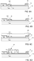
- Figure 6A shows a cross-section similar to Figure 3 in an intermediate manufacturing step of the HEMT transistor 50.
- Figure 6A shows an intermediate structure, wherein, above the semiconductor body 52, the lower portion 70A of the source metallization 70, the lower portion 72A of the drain metallization 72, and the first insulating layer 58 have already been formed in a per se known manner; furthermore, the first insulating layer 58 has been etched to form the first opening 61; the lower gate portion 60A in the first opening 61 and the first intermediate gate portion 60C above the lower gate portion 60A have been formed (for example, the lower gate portion 60A and the first intermediate gate portion 60C may be formed simultaneously, by physical vapor deposition (PVD) of a nickel layer within a cavity formed in a temporary structure and having a small-sized opening, related to the area of the first intermediate gate portion 60C) and, after removing the temporary structure, the dielectric layer 82 has been deposited, for example by PECVD deposition.
- PVD physical vapor deposition
- a portion of the dielectric layer 82 is removed, for example by dry etching, above the first intermediate gate portion 60C, forming the second opening 83.
- the first field plate region 84 may be formed without adding process steps with respect to the manufacturing process of the HEMT transistor 30 of Figure 2 , only through an etching mask modification of the metal layer 200, and thus without additional costs.
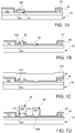
- Figure 7A shows a cross-section similar to Figure 4 in an intermediate manufacturing step of the HEMT transistor 100.
- Figure 7A shows an intermediate structure wherein, above the semiconductor body 52, the lower portion 70A of the source metallization 70, the lower portion 72A of the drain metallization 72 and the first insulating layer 58' have already been formed, in a per se known manner; furthermore, the first insulating layer 58' has already been etched to form the first opening 61, the lower gate portion 60A in the first opening 61 and the first intermediate gate portion 60C above the lower gate portion 60A have already been formed (for example, the lower gate portion 60A and the first intermediate gate portion 60C may be formed as described above for the HEMT transistor 50) and the dielectric layer 82' has been deposited, for example by PECVD deposition.
- the intermediate structure of Figure 7A is thus identical to that of Figure 6A .
- a portion of the dielectric layer 82' is removed above the first intermediate gate portion 60C, forming the second opening 83. Furthermore, a portion of the dielectric layer 82' and the underlying portion of the first insulating layer 58' are selectively removed, laterally to the second opening 83, where it is desired to form the first field plate region 84', forming the third opening 86.
- a gate metal layer 200' is deposited, for example in the manner described above with reference to Figure 6C , carrying out in succession a first sputtering process, of tungsten nitride (WN) or tantalum nitride (TaN), to form a first metal layer (which is thinner and intended to subsequently form the second intermediate gate portion 60D and the lower portion 84A of the first field plate region 84) and a second sputtering process, for example of aluminium, to form a second metal layer, which is thicker.
- a first sputtering process of tungsten nitride (WN) or tantalum nitride (TaN)
- a second sputtering process for example of aluminium
- FIG. 7D for example using a resist mask not shown, portions of the gate metal layer 200' are selectively removed, completing the gate region 60 and the first field plate region 84'.
- deposition of the second insulating layer 62 deposition of a third metal layer, for example aluminium-based (as indicated above) by sputtering and subsequent selective removal to form the upper portions 70B and 72B of the source and drain metallizations 70, 72 and the second field plate region 85.
- deposition of the passivation layer 66 follows.
- the first field plate region 84 may be formed without adding process steps with respect to the manufacturing process of the HEMT transistor 30 of Figure 2 , through an etching mask modification of the gate metal layer 200', and thus without additional costs.
- the manufacturing process of the HEMT transistor 150 does not require additional steps with respect to those foreseen for forming the HEMT transistor 1 of Figure 1 , only requiring modification of the mask used to define the gate region 60" in order to form the first field plate region 84".
- the HEMT device shown in Figures 3-5 has many advantages. As indicated, due to the presence of an additional shielding region (first field plate region 84, 84', 84"), the HEMT device described has a high gain, as shown in Figure 8 .
- Figure 8 shows the result of simulations carried out by the Applicant relative to the plot of the gain G obtainable with the HEMT transistor as a function of the frequency f in the range 2-10 GHz, for the HEMT transistor 1 of Figure 1 (curve A), the HEMT transistor 30 of Figure 2 (curve B), the HEMT transistor 50 of Figure 3 (curve C) and the HEMT transistor 100 of Figure 4 (curve D), respectively.
- the HEMT transistors 50 and 100 have a considerably greater gain with respect to the similar structures lacking the first field plate region 84, 84'.
- the HEMT device shown in Figures 3-5 allows a not negligible improvement to be obtained also as regards electric field uniformity and thus its robustness at high voltages.
- the second field plate 85 and the first field plate 84, 84', 84" may be connected in various ways to the source metallization 70; the first field plate 84" and the gate region 60" in Figure 5 may be positioned in different ways with respect to the insulating layer 58"; and the gate region 60" in Figure 5 may be defined in different ways, as discussed in detail hereinafter.
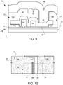
- Figure 9 shows an embodiment where the HEMT transistor 150 of Figure 5 has the second field plate 85 connected to the source metallization 70 through a connecting portion formed in the third metal layer which also forms the upper portion 70B of the source metallization 70, the upper portion 72B of the drain metallization 72 and the second field plate region 85, and thus defined in the same etching step.
- the second field plate 85 is connected to the source metallization 70 through a connecting region extending over the inactive area of the HEMT transistor 150, as described hereinbelow with reference to Figure 10 , which shows the structure of an elementary cell of the HEMT transistor 150 of Figure 5 in a plan view.
- the HEMT transistor 150 may comprise a plurality of elementary cells, each having at least one source metallization 70, at least one drain metallization 72, at least one first field plate 84, and at least one second field plate 85, extending as fingers along a direction (vertical direction of Figure 10 ).
- Figure 10 shows a portion of an intermediate structure of the HEMT transistor 150 after depositing and defining the second insulating layer 62 (not visible in Figure 10 ) and depositing and defining a third metal layer, indicated by 98, to form the upper portions 70B and 72B of the source and drain metallizations 70, 72 and the second field plate region 85.
- Figure 10 shows the active area 90 (which accommodates high mobility conduction electrons of the 2-deg), surrounded by the inactive area 91, not participating to the conduction action.
- the inactive area 91 is generally doped, to avoid passage of current when the HEMT transistor 150 is switched off.
- line 93 indicates the boundary of the active area 90.
- the third metal layer 98 is also defined to form a second field plate connecting region 97 extending over the inactive area 91 between the upper portion 70B of the source metallization 70 and the second field plate region 85, thereby connecting them electrically.
- the second field plate 85 is connected to the source metallization 70 by both the second field plate connecting region of Figure 10 and the clips 105 of Figure 11 .
- the first field plate 84, 84', 84" may be connected to the source metallization 70 through connecting regions extending over the inactive area 91 or through the second field plate 85, as explained below.
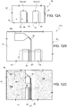
- first field plate 84, 84', 84" may be connected to the source metallization 70 as shown in Figures 12A-12C , which show the structure of an elementary cell of the HEMT transistor 150 of Figure 5 in three intermediate manufacturing steps (connection over the inactive area 91).
- the HEMT transistor 150 may comprise a plurality of elementary cells, each having at least one source metallization 70, at least one drain metallization 72, at least one first field plate 84, and at least one second field plate 85, extending as fingers along a direction (vertical direction of Figures 12A-12C ).
- the lower portions 70A, 72A of the source 70 and drain metallizations 72 extend mainly on the active area 90 and have ends portions 70A1, 72A1 extending on the inactive area 91.
- Line 93 indicates the boundary of the active area 90;
- line 94 indicates the boundary of insulating layer 58" (not visible) and
- line 95 indicates the first opening (61" in Figure 5 ).
- Figure 12B shows the same portion of the intermediate structure of the HEMT transistor 150 after depositing and defining a metal layer (similar to gate metal layer 200' of Figure 7C ), so as to form the gate region 60", the first field plate 84" and a first connecting region 96.
- the first connecting region 96 is integral with and in prosecution of the first field plate 84", extends from and end of the first field plate 84" onto the inactive area 91 and ends with an enlarged portion 96A.
- the second insulating layer 62 ( Figure 5 ) has been defined to form a through opening 99 over the enlarged portion 96A of the first connecting region 96.
- the third metal layer 98 also extends over the inactive region 91 and in particular over the enlarged portion 96A and fills the through opening 99 to form a connection via (indicated by the same number 99 since it has the same shape as the through opening).
- the connection via 99 electrically connects the upper portion 70B of the source metallization 70 to the enlarged portion 96A of the first connecting region 96 (at a lower level) and thus to the first field plate 84".
- the third metal layer 98 is also defined to form the second field plate connecting region 97 extending over the inactive area 91 between the upper portion 70B of the source metallization 70 and the second field plate region 85.
- first connecting region 96, the connection via 99 and the second connecting region 97 form line 75 of Figure 3 , directly connecting the source metallization 70, the first field plate 84" and the second field plate region 85.
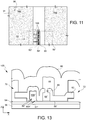
- the first field plate 84, 84', 84" may be connected to the source metallization 70 through the second field plate 85, as shown in Figure 13 .
- the first field plate 84, 84', 84" may be connected to the source metallization 70 both over the inactive area 91(through the first connecting region 96, the enlarged portion 96A, and the connection via 99, Figures 12A-12C ) and over the active area 90 (through the field plate connection via 89, Figure 13 ), combining the solutions of Figures 12A-12C and Figure 13 .
- the first field plate 84" may be arranged in different ways with respect to the insulating layer 58".
- the first field plate 84" may be formed with its lower portion inside the insulating layer 58", as shown in Figure 14 .
- process steps similar to those described with reference to figures 7B-7D are performed.
- the first opening 61 and, in a separate etching step a cavity 87' (corresponding to the third opening 86 and the cavity 87 of Figure 4 ) are formed.
- the gate metal layer (analogous to gate metal layer 200" of Figure 7C ) is deposited and defined to form the gate region 60" and the first field plate region 84".
- the second insulating layer 62 and the third metal layer are deposited and defined and covered by the passivation layer 66.
- the first field plate 84" may be formed to contact the semiconductor body 52.
- the insulating layer 58" may be removed only partially, as shown in Figure 15 .
- the gate region 60" may extend directly on and physical in contact with the semiconductor body 52, as shown in Figures 9 , 12 , 13-15 or may enter a recess in the semiconductor body 52, as shown in Figure 16 .
- a lower gate portion 60A" of the gate 60" extends through part of the upper layer 56 of the semiconductor body 52 in a recess 79.
- This solution may be used when the first field plate 84" is in direct contact with the semiconductor body 52.
- the gate region 60" and the first field plate 84" may be defined through known masking and etching steps, in which case the insulating layer 58" is slightly recessed as a consequence of the etching process, as shown in Figures 9 , 13-17 or using a lift-off process. In this case, as shown in Figure 17 , the insulating layer 58" has a planar upper surface, not recessed.
Landscapes
- Junction Field-Effect Transistors (AREA)
Abstract
Description
- The present invention relates to a High Electron Mobility Transistor (HEMT) including field plate regions and the manufacturing process thereof.
- As known, the HEMT transistors, also known as heterostructure field effect transistors (HFET), are finding wide diffusion, because of the possibility of operating at high voltages, as well as at high breakdown voltages.
- In each HEMT transistor, a semiconductive heterostructure allows a so-called 2-dimensional electron gas (2deg), forming a channel region of the HEMT transistor, to be generated in an electronically controllable manner. Furthermore, each HEMT transistor comprises a gate region; the HEMT transistor channel is modulated by the voltage on the gate region.
- For example,
Figure 1 shows aHEMT transistor 1, comprising asemiconductor body 2, here formed by a first and asecond layers lower layer 4 andupper layer 6. - The
lower layer 4 is formed by a first semiconductor material, such as for example a first semiconductive alloy of elements of the groups III and V of the periodic table; for example, thelower layer 4 may be formed by gallium nitride (GaN). - The
upper layer 6 overlies, and is in direct contact with, thelower layer 4, and is formed by a second semiconductor material, such as for example a second semiconductive alloy, different from the first semiconductive alloy, of elements of the groups III-V of the periodic table. For example, theupper layer 6 may be formed by aluminium gallium nitride (AlGaN). Thelower layer 4 and theupper layer 6 are for example of N-type. Although not shown, thesemiconductor body 2 further comprises a substrate, typically formed by silicon, on which thelower layer 4 is formed. - The
HEMT transistor 1 further comprises asource metallization 20 and adrain metallization 22 arranged, at a mutual distance, above theupper layer 6. Thesource metallization 20 and thedrain metallization 22 may be in direct ohmic contact with respective source and drain regions, as taught, e.g., inUS 2020/0168718 (corresponding toEP 3 660 923A1 ). In particular, thesource 20 anddrain metallizations 22 have a respectivelower portion upper layer 6, and a respectiveupper portion lower portion source 20 anddrain metallizations 22 are for example of titanium and aluminium or multi-layer stacks. - A first
insulating layer 8, for example of silicon nitride, extends above theupper layer 6 and part of thelower portions source 20 anddrain metallizations 22. Furthermore, the firstinsulating layer 8 has anopening 11 arranged at an intermediate position between thelower portions source 20 anddrain metallizations 22. - A
gate region 10, of conductive material, extends partly within the opening 11 (with alower gate portion 10A) and partly above the first insulating layer 8 (with anupper gate portion 10B). Thegate region 10 is formed, for example, by a stack of materials, such as nickel (Ni), gold (Au), platinum (Pt) and palladium (Pd), with the nickel layer directly in contact withupper layer 6 and forming therewith a metal-semiconductor junction of the Schottky type, that is rectifying. - A second
insulating layer 12, for example of silicon nitride, extends above the firstinsulating layer 8 and surrounds theupper gate portion 10A. In practice, the secondinsulating layer 12 and the firstinsulating layer 8 form aninsulating structure 13 sealing thegate region 10. - A
field plate region 14 extends above the secondinsulating layer 12, partly vertically overlying thegate region 10 and partly laterally offset, towards thedrain metallization region 22. Thefield plate region 14, for example of aluminium, has the aim of modifying the existing electric field during operation of theHEMT transistor 1. Thefield plate region 14 is electrically coupled to thesource metallization 20, in a not shown manner. - A
passivation layer 16, for example of silicon oxide, surrounds theupper portions source 20 anddrain metallizations 22 and thefield plate region 14 and covers the whole structure. - Another embodiment of a HEMT transistor is described in Italian patent application
102018000011065 filed on 13 December 2018 EP 3667735 ) and allows the drain leakage current to be reduced. This solution is shown inFigure 2 , slightly modified with respect to what shown in the aforementioned patent application, to highlight the differences with respect to theHEMT transistor 1. -
Figure 2 shows aHEMT transistor 30 having a general structure similar to the one of theHEMT transistor 1 ofFigure 1 ; therefore like parts are identified with the same reference numbers and will no longer be described. - In the
HEMT transistor 30 ofFigure 2 , theinsulation structure 13 comprises, in addition to the first and secondinsulating layers dielectric layer 32 extending between them and, partly, within thegate region 10. Thedielectric layer 32 may also be of silicon nitride. In this way, thegate region 10, besides having alower gate portion 10A and anupper gate portion 10B, has a first and a secondintermediate gate portion lower gate portion 10A and theupper gate portion 10B. - In detail, the first
intermediate gate portion 10C is contiguous to thelower gate portion 10A, extends above the firstinsulating layer 8 and has an area (in a cross-section perpendicular to the drawing plane) approximately equal to that of theupper gate portion 10B. The secondintermediate gate portion 10D is arranged between the firstintermediate gate portion 10C and theupper gate portion 10B, in physical continuity with them, and has an area (in a cross-section perpendicular to the drawing plane) smaller than the area of the firstintermediate gate portion 10C and theupper gate portion 10B. The secondintermediate gate portion 10D has a thickness approximately equal to that of thedielectric layer 32. - In practice, the
dielectric layer 32 extends partly laterally to the firstintermediate gate portion 10C and partly (with a substantially annular portion thereof) between the first and the secondintermediate gate portions intermediate portion 10D. - This allows the
gate region 10 to be made by three different alloys (not shown); specifically, thelower gate portion 10A and the firstintermediate portion 10C may be of a first metal (for example, nickel Ni) forming a Schottky contact with thebody 2; theupper gate portion 10B may be of a second metal (for example, aluminium Al) having low resistance; and the secondintermediate portion 10D may be of a third material (for example, tungsten nitride WN or tantalum nitride TaN or TiN), which serves as a barrier layer and prevents the aluminium of theupper gate portion 10B from diffusing, through the firstintermediate portion 10C and thelower gate portion 10A, down to theupper layer 6 of thebody 2, which would lead to damaging the Schottky junction. - The structures shown in
Figures 1 and 2 have a very good behaviour in frequency, from frequencies lower than 6GHz up to frequencies in the range 30-50 GHz (millimetre-waves), and very good switching capacities, but are susceptible of improvement as regards the gain and electric field uniformity when high voltages are applied to the gate region. - The aim of the present invention is to provide an improved HEMT transistor.
- According to the present invention, a HEMT transistor and the manufacturing process thereof are provided, as defined in the attached claims.
- For a better understanding of the present invention, some embodiments thereof are now described, purely by way of non-limiting example, with reference to the attached drawings, wherein:
-
Figure 1 schematically shows a cross-section of a known HEMT transistor; -
Figure 2 schematically shows a cross-section of another HEMT transistor; -
Figure 3 schematically shows a cross-section of an embodiment of the present HEMT transistor; -
Figure 4 schematically shows a cross-section of a different embodiment of the present HEMT transistor; -
Figure 5 schematically shows a cross-section of another embodiment of the present HEMT transistor; -
Figures 6A-6D show cross-sections similar to that ofFigure 3 , in subsequent manufacturing steps; -
Figures 7A-7D show cross-sections similar toFigure 4 , in subsequent manufacturing steps; and -
Figure 8 shows the result of simulations carried out by the Applicant on the structures ofFigures 1, 2 ,3 and 4 ; -
Figure 9 is cross-section of another embodiment of the present HEMT transistor; -
Figures 10 and11 are top plan views of different embodiments of the present HEMT transistor; -
Figure 12A-12C are top plan views of part of the HEMT transistor ofFigure 5 , in subsequent manufacturing steps, according to an embodiment; and -
Figures 13-17 are cross-sections of other embodiments of the present HEMT transistor. -
Figure 3 shows aHEMT transistor 50 according to an embodiment. - The
HEMT transistor 50 has a general structure similar to theHEMT transistor 30 ofFigure 2 , thus briefly described herein below; the regions thereof have been identified by numbers incremented by 50. - The
HEMT transistor 50 comprises asemiconductor body 52, here formed by alower layer 54, for example, of gallium nitride (GaN), and anupper layer 56, for example, of aluminium gallium nitride (AlGaN). Theupper layer 56 forms asurface 52A of thesemiconductor body 52. In a not shown manner, thesemiconductor body 52 may further comprise a silicon substrate and/or theupper layer 56 may be a multilayer, including layers of AlGaN with different percentage of aluminum (for example one AlGaN layer with 20% of aluminum and another AlGaN layer with 40%). - A
source metallization 70 and adrain metallization 72 extend, at a mutual distance, above thebody 52. Also here, thesource 70 anddrain metallizations 72 compriselower portions upper portions source 70 anddrain metallizations 72 form source and drain electrodes and are electrically coupled to respective source and drain terminals S, D. - A first
insulating layer 58, for example of silicon nitride, extends above theupper layer 56 and part of thelower portions source 70 anddrain metallizations 72. - A
gate region 60, of conductive material, extends above thesemiconductor body 52 and comprises alower gate portion 60A (extending into an opening, calledfirst opening 61, of thefirst insulating layer 58, and in direct contact with theupper layer 56 of the semiconductor body 52), anupper gate portion 60B, a firstintermediate gate portion 60C and a secondintermediate gate portion 60D, arranged between thelower gate portion 60A and theupper gate portion 60B. Here again, thegate region 60 may be formed by a stack of materials, for example nickel (Ni), aluminium Al and tungsten nitride (WN) or tantalum nitride (TaN). - The
gate region 60 is electrically coupled to a gate terminal G. - A
dielectric layer 82, for example of silicon nitride, extends above the firstinsulating layer 58 and, partly, within thegate region 60. Therefore thedielectric layer 82 has an opening (also called second opening 83) wherein the secondintermediate portion 60D of thegate region 60 extends. - A second insulating
layer 62, for example of silicon nitride, extends above thedielectric layer 82 and surrounds theupper gate portion 60A on the top and laterally. In practice, the second insulatinglayer 62 forms, with the first insulatinglayer 58 and thedielectric layer 82, aninsulation structure 63 sealing thegate region 60. - A
passivation layer 66, for example of silicon oxide, surrounds theupper portions metallizations - The
transistor 50 ofFigure 3 has a first and a secondfield plate region - The first
field plate region 84 extends above thedielectric layer 82, between thegate region 60 and thedrain metallization 72, and is covered by the second insulatinglayer 62. In the embodiment shown, the firstfield plate region 84 is arranged closer to thegate region 60 than to thedrain metallization 72. For example, in the direction in which thesource metallization 70, thegate region 60, the firstfield plate region 84 and thedrain metallization 72 are adjacent (direction parallel to a first Cartesian axis X inFigure 3 ), the firstfield plate region 84 may have a width L1 depending on the breakdown voltage, for example comprised between 0.1 and 3 µm, for example of 1 µm, and may be arranged at a distance d of 0.1 to 3 µm, for example of 1 µm from the gate region 60 (the distance d being calculated, approximately, from the edge of theupper gate portion 60B facing the first field plate region 84). - The first
field plate region 84 may be of a same conductive material, in particular of the same metal layer, and manufactured in the same manufacturing step as theupper gate portion 60B, as discussed in detail below with reference toFigures 6A-6D . - The second
field plate region 85 extends above the second insulatinglayer 62, vertically overlying (with respect to a second Cartesian axis Z) the firstfield plate region 84, and is covered by thepassivation layer 66. The secondfield plate region 85 has a width L2 at least equal to, but generally greater than, the width L1 of the firstfield plate region 84. For example, the width L2 of the secondfield plate region 85 may be comprised between 0.1 and 5 µm. - The
field plate regions source metallization 70, as shown bylines 75. In particular, the secondfield plate region 85 may be formed together with and using the same metal layer as theupper portions regions - The
field plate regions HEMT transistor 50. Furthermore, the presence of the firstfield plate region 84 allows the gain of theHEMT transistor 50 to be considerably increased. In fact, in case of an increase in the drain voltage, the firstfield plate region 84, acting as a shield between thegate region 60 and thedrain metallization 72, has the effect of decreasing the gate-drain capacity to which the gain is inversely related, as discussed below with reference toFigure 8 . -
Figure 4 shows a different embodiment of a HEMT transistor, here indicated with 100. - The
HEMT transistor 100 has a general structure similar to theHEMT transistor 50 ofFigure 3 . The common parts have thus been provided with the same reference numbers and will not be further described. - In the
HEMT transistor 100, the first field plate region, here indicated with 84', comprises alower plate portion 84A' and anupper plate portion 84B'. - The
upper plate portion 84B' of the first field plate region 84' roughly corresponds to the firstfield plate region 84 ofFigure 3 , and thus extends above the second insulatinglayer 62, laterally to thegate region 60, between the same and thedrain metallization 72. Thelower plate portion 84A' of the first field plate region 84' extends continuously from theupper plate portion 84B' towards thesurface 52A of thesemiconductor body 52 through an opening (called third opening 86) of the dielectric layer, here indicated with 82', and, partially, through the first insulating layer, here indicated with 58', in acavity 87 thereof. Thelower plate portion 84A', however, does not completely extend through the first insulating layer 58' and a thinner portion thereof, below referred to as thinnedportion 58A', extends between thesurface 52A of thesemiconductor body 52 and the first field plate region 84', electrically separating the latter from thesemiconductor body 52. - This embodiment is characterized by a marked increase in gain and a particularly uniform electric field, as discussed below with reference to
Figure 8 . -
Figure 5 shows another embodiment of a HEMT transistor, here indicated with 150. - The
HEMT transistor 150 has a general structure similar to theHEMT transistor 50 ofFigure 3 , except for the shape of the gate region (similar to theHEMT transistor 1 ofFigure 1 ). The parts in common with theHEMT transistor 50 ofFigure 3 have thus been provided with the same reference numbers and will not be further described. - In detail, the
HEMT transistor 150 comprises agate region 60" having alower gate portion 60A" and anupper gate portion 60B". Furthermore, theHEMT transistor 150 comprises a first insulating layer, indicated with 58" and having anopening 61" accommodating thelower gate portion 60A", and a firstfield plate region 84". The firstfield plate region 84" extends above the insulatinglayer 58" and is coated, laterally and on the top, by the second insulatinglayer 62. - In this embodiment, the
lower gate portion 60A" and theupper gate portion 60B" may be formed by a single deposited (for example "sputtered") metal layer or a single evaporated layer or by a stack of layers deposited separately. In the latter case, the firstfield plate region 84" may be formed with one of the layers of thegate region 60". - Here again, the second
field plate region 85 extends vertically (in direction of the second Cartesian axis Z) above the firstfield plate region 84". - This embodiment allows a simplification of the manufacturing process, due to the simple shape of the
gate region 60". - The manufacturing process of the
HEMT transistors Figures 3 and 4 will now be described, with reference toFigures 6A-6D and, respectively, 7A-7D.Figure 6A shows a cross-section similar toFigure 3 in an intermediate manufacturing step of theHEMT transistor 50. - In particular,
Figure 6A shows an intermediate structure, wherein, above thesemiconductor body 52, thelower portion 70A of thesource metallization 70, thelower portion 72A of thedrain metallization 72, and the first insulatinglayer 58 have already been formed in a per se known manner; furthermore, the first insulatinglayer 58 has been etched to form thefirst opening 61; thelower gate portion 60A in thefirst opening 61 and the firstintermediate gate portion 60C above thelower gate portion 60A have been formed (for example, thelower gate portion 60A and the firstintermediate gate portion 60C may be formed simultaneously, by physical vapor deposition (PVD) of a nickel layer within a cavity formed in a temporary structure and having a small-sized opening, related to the area of the firstintermediate gate portion 60C) and, after removing the temporary structure, thedielectric layer 82 has been deposited, for example by PECVD deposition. - Next,
Figure 6B , a portion of thedielectric layer 82 is removed, for example by dry etching, above the firstintermediate gate portion 60C, forming thesecond opening 83. - Then,
Figure 6C , two sputtering processes are carried out in succession; in particular a first sputtering process, of tungsten nitride (WN) or tantalum nitride (TaN), forms a first metal layer, which is thinner, fills thesecond opening 83 and is intended to subsequently form the secondintermediate gate portion 60D, and a second sputtering process, for example of aluminium, forms a second metal layer which is thicker. The layer formed of the first and second metal layers is indicated with 200 inFigure 6C . Alternatively, a sequence of sputtered metal layers, including tungsten nitride/aluminium/titanium nitride WN/Al/TiN may be used. - Next,
Figure 6D , for example using a resist mask not shown, portions of the metal layer 200 (also called gate metal layer) are selectively removed, forming the secondintermediate gate portion 60D and theupper portion 60B of thegate region 60, as well as the firstfield plate region 84. - Known steps follow, including deposition of the second insulating
layer 62, deposition of a third metal layer, for example aluminium based (such as an Al, AlSiCu or AlCu bilayer and a Ti, TiN metal layer) by sputtering and subsequent selective removal to form theupper portions metallizations field plate region 85. Finally the deposition of thepassivation layer 66 follows. - In this way, the first
field plate region 84 may be formed without adding process steps with respect to the manufacturing process of theHEMT transistor 30 ofFigure 2 , only through an etching mask modification of themetal layer 200, and thus without additional costs. -
Figure 7A shows a cross-section similar toFigure 4 in an intermediate manufacturing step of theHEMT transistor 100. - In particular,
Figure 7A shows an intermediate structure wherein, above thesemiconductor body 52, thelower portion 70A of thesource metallization 70, thelower portion 72A of thedrain metallization 72 and the first insulating layer 58' have already been formed, in a per se known manner; furthermore, the first insulating layer 58' has already been etched to form thefirst opening 61, thelower gate portion 60A in thefirst opening 61 and the firstintermediate gate portion 60C above thelower gate portion 60A have already been formed (for example, thelower gate portion 60A and the firstintermediate gate portion 60C may be formed as described above for the HEMT transistor 50) and the dielectric layer 82' has been deposited, for example by PECVD deposition. The intermediate structure ofFigure 7A is thus identical to that ofFigure 6A . - Next,
Figure 7B , a portion of the dielectric layer 82' is removed above the firstintermediate gate portion 60C, forming thesecond opening 83. Furthermore, a portion of the dielectric layer 82' and the underlying portion of the first insulating layer 58' are selectively removed, laterally to thesecond opening 83, where it is desired to form the first field plate region 84', forming thethird opening 86. - Then,
Figure 7C , a gate metal layer 200' is deposited, for example in the manner described above with reference toFigure 6C , carrying out in succession a first sputtering process, of tungsten nitride (WN) or tantalum nitride (TaN), to form a first metal layer (which is thinner and intended to subsequently form the secondintermediate gate portion 60D and thelower portion 84A of the first field plate region 84) and a second sputtering process, for example of aluminium, to form a second metal layer, which is thicker. - Next,
Figure 7D , for example using a resist mask not shown, portions of the gate metal layer 200' are selectively removed, completing thegate region 60 and the first field plate region 84'. - Known steps follow, including deposition of the second insulating
layer 62, deposition of a third metal layer, for example aluminium-based (as indicated above) by sputtering and subsequent selective removal to form theupper portions metallizations field plate region 85. Finally, the deposition of thepassivation layer 66 follows. - Also in this case, the first
field plate region 84 may be formed without adding process steps with respect to the manufacturing process of theHEMT transistor 30 ofFigure 2 , through an etching mask modification of the gate metal layer 200', and thus without additional costs. - Similarly, the manufacturing process of the
HEMT transistor 150 does not require additional steps with respect to those foreseen for forming theHEMT transistor 1 ofFigure 1 , only requiring modification of the mask used to define thegate region 60" in order to form the firstfield plate region 84". - The HEMT device shown in
Figures 3-5 has many advantages. As indicated, due to the presence of an additional shielding region (firstfield plate region Figure 8 . - In particular,
Figure 8 shows the result of simulations carried out by the Applicant relative to the plot of the gain G obtainable with the HEMT transistor as a function of the frequency f in the range 2-10 GHz, for theHEMT transistor 1 ofFigure 1 (curve A), theHEMT transistor 30 ofFigure 2 (curve B), theHEMT transistor 50 ofFigure 3 (curve C) and theHEMT transistor 100 ofFigure 4 (curve D), respectively. As visible, theHEMT transistors field plate region 84, 84'. - In a not shown manner, the HEMT device shown in
Figures 3-5 allows a not negligible improvement to be obtained also as regards electric field uniformity and thus its robustness at high voltages. - Finally, it is clear that modifications and variations may be made to the HEMT transistor and the manufacturing process thereof described and illustrated herein without thereby departing from the scope of the present invention, as defined in the attached claims. For example, the different embodiments described may be combined so as to provide further solutions.
- For example, the
second field plate 85 and thefirst field plate source metallization 70; thefirst field plate 84" and thegate region 60" inFigure 5 may be positioned in different ways with respect to the insulatinglayer 58"; and thegate region 60" inFigure 5 may be defined in different ways, as discussed in detail hereinafter. - The
second field plate 85 may be connected to the source metallization 70 through connecting regions extending either over an active area (where the 2-dimensional electron gas - 2deg- forms a channel region of the HEMT transistor and conducts current) or an inactive area surrounding the active area, as explained below. - For example,
Figure 9 shows an embodiment where theHEMT transistor 150 ofFigure 5 has thesecond field plate 85 connected to the source metallization 70 through a connecting portion formed in the third metal layer which also forms theupper portion 70B of thesource metallization 70, theupper portion 72B of thedrain metallization 72 and the secondfield plate region 85, and thus defined in the same etching step. - In particular, in
Figure 9 , a biasingmetal portion 88 of the third metal layer extends on the second insulatinglayer 62 between theupper portion 70B of thesource metallization 70 and the secondfield plate region 85 and forms a single region with them. - According to a different embodiment, the
second field plate 85 is connected to the source metallization 70 through a connecting region extending over the inactive area of theHEMT transistor 150, as described hereinbelow with reference toFigure 10 , which shows the structure of an elementary cell of theHEMT transistor 150 ofFigure 5 in a plan view. - It is intended that the
HEMT transistor 150 may comprise a plurality of elementary cells, each having at least onesource metallization 70, at least onedrain metallization 72, at least onefirst field plate 84, and at least onesecond field plate 85, extending as fingers along a direction (vertical direction ofFigure 10 ). -
Figure 10 shows a portion of an intermediate structure of theHEMT transistor 150 after depositing and defining the second insulating layer 62 (not visible inFigure 10 ) and depositing and defining a third metal layer, indicated by 98, to form theupper portions metallizations field plate region 85. In particular,Figure 10 shows the active area 90 (which accommodates high mobility conduction electrons of the 2-deg), surrounded by theinactive area 91, not participating to the conduction action. Theinactive area 91 is generally doped, to avoid passage of current when theHEMT transistor 150 is switched off. - In
figure 10 ,line 93 indicates the boundary of theactive area 90. - Here, the
third metal layer 98 is also defined to form a second fieldplate connecting region 97 extending over theinactive area 91 between theupper portion 70B of thesource metallization 70 and the secondfield plate region 85, thereby connecting them electrically. - According to a different embodiment,
Figure 11 , thesecond field plate 85 is connected to the source metallization 70 through a plurality of clips orbridge portions 105 extending at a distance to each other over theactive area 90 and formed by thesecond metal layer 200". In this case, in a cross-section, theclips 105 are not visible (as inFigure 5 ) or have a shape similar to the biasingmetal portion 88 ofFigure 9 , depending on whether the cross section through theHEMT transistor 150 is drawn in an area between twoadjacent clips 105 or crosses one of theclips 105. - According to still another embodiment, the
second field plate 85 is connected to the source metallization 70 by both the second field plate connecting region ofFigure 10 and theclips 105 ofFigure 11 . - The
first field plate inactive area 91 or through thesecond field plate 85, as explained below. - For example, the
first field plate Figures 12A-12C , which show the structure of an elementary cell of theHEMT transistor 150 ofFigure 5 in three intermediate manufacturing steps (connection over the inactive area 91). - Also here, the
HEMT transistor 150 may comprise a plurality of elementary cells, each having at least onesource metallization 70, at least onedrain metallization 72, at least onefirst field plate 84, and at least onesecond field plate 85, extending as fingers along a direction (vertical direction ofFigures 12A-12C ). -
Figure 12A shows a portion of the intermediate structure of theHEMT transistor 150 after forming thelower portions metallizations layer 58" (Figure 5 ) . - In
figure 12A , thelower portions source 70 and drain metallizations 72 extend mainly on theactive area 90 and have ends portions 70A1, 72A1 extending on theinactive area 91.Line 93 indicates the boundary of theactive area 90;line 94 indicates the boundary of insulatinglayer 58" (not visible) andline 95 indicates the first opening (61" inFigure 5 ). -
Figure 12B shows the same portion of the intermediate structure of theHEMT transistor 150 after depositing and defining a metal layer (similar to gate metal layer 200' ofFigure 7C ), so as to form thegate region 60", thefirst field plate 84" and a first connectingregion 96. The first connectingregion 96 is integral with and in prosecution of thefirst field plate 84", extends from and end of thefirst field plate 84" onto theinactive area 91 and ends with anenlarged portion 96A. -
Figure 12C shows the same portion ofFigures 12A and 12B after depositing and defining the second insulating layer 62 (not visible inFigure 12C ) and depositing and defining the third metal layer, indicated again by 98, to form theupper portions metallizations field plate region 85. - In
Figure 12C , the second insulating layer 62 (Figure 5 ) has been defined to form a throughopening 99 over theenlarged portion 96A of the first connectingregion 96. - Here, the
third metal layer 98 also extends over theinactive region 91 and in particular over theenlarged portion 96A and fills the throughopening 99 to form a connection via (indicated by thesame number 99 since it has the same shape as the through opening). The connection via 99 electrically connects theupper portion 70B of the source metallization 70 to theenlarged portion 96A of the first connecting region 96 (at a lower level) and thus to thefirst field plate 84". - Here, in addition, the
third metal layer 98 is also defined to form the second fieldplate connecting region 97 extending over theinactive area 91 between theupper portion 70B of thesource metallization 70 and the secondfield plate region 85. - Therefore, the first connecting
region 96, the connection via 99 and the second connectingregion 97form line 75 ofFigure 3 , directly connecting thesource metallization 70, thefirst field plate 84" and the secondfield plate region 85. - According to a different embodiment, the
first field plate second field plate 85, as shown inFigure 13 . - In detail, in
Figure 13 , the second insulatinglayer 62 has a through opening, called fieldplate connection opening 89, extending over thefirst field plate 84". Thereby, during deposition of thethird metal layer 98, the metal enters and fills the fieldplate connection opening 89, forming a field plate via also indicated by 89 (since it has the same shape and is defined by the field plate connection opening 89). The field plate connection via 89 electrically connects thefirst field plate 84" to the secondfield plate region 85 and thus, through one of the solutions discussed above in section Connection of thesecond field plate 85, to thesource metallization 70. - According to another embodiment, the
first field plate region 96, theenlarged portion 96A, and the connection via 99,Figures 12A-12C ) and over the active area 90 (through the field plate connection via 89,Figure 13 ), combining the solutions ofFigures 12A-12C andFigure 13 . - The
first field plate 84" may be arranged in different ways with respect to the insulatinglayer 58". - In particular, as an alternative to the arrangement shown in
Figure 5 , where thefirst field plate 84" is formed completely over the insulatinglayer 58", thefirst field plate 84" may be formed with its lower portion inside the insulatinglayer 58", as shown inFigure 14 . - In this case, process steps similar to those described with reference to
figures 7B-7D are performed. In particular, after depositing the insulatinglayer 58", thefirst opening 61 and, in a separate etching step, a cavity 87' (corresponding to thethird opening 86 and thecavity 87 ofFigure 4 ) are formed. Then, the gate metal layer (analogous togate metal layer 200" ofFigure 7C ) is deposited and defined to form thegate region 60" and the firstfield plate region 84". Thereafter, the second insulatinglayer 62 and the third metal layer are deposited and defined and covered by thepassivation layer 66. - According to a different embodiment, the
first field plate 84" may be formed to contact thesemiconductor body 52. In this case, the insulatinglayer 58" may be removed only partially, as shown inFigure 15 . - In detail, in
Figure 15 , the third opening in the insulatinglayer 58" (here, indicated by 86') is a through opening, so that the bottom portion of thefirst field region 4" directly contacts thesemiconductor body 52. - The
gate region 60" may extend directly on and physical in contact with thesemiconductor body 52, as shown inFigures 9 ,12 ,13-15 or may enter a recess in thesemiconductor body 52, as shown inFigure 16 . - In
Figure 16 , alower gate portion 60A" of thegate 60" extends through part of theupper layer 56 of thesemiconductor body 52 in arecess 79. - This solution may be used when the
first field plate 84" is in direct contact with thesemiconductor body 52. - The
gate region 60" and thefirst field plate 84" may be defined through known masking and etching steps, in which case the insulatinglayer 58" is slightly recessed as a consequence of the etching process, as shown inFigures 9 ,13-17 or using a lift-off process. In this case, as shown inFigure 17 , the insulatinglayer 58" has a planar upper surface, not recessed.
Claims (17)
- A HEMT transistor (50; 100; 150) comprising:a semiconductor body (52) having a semiconductive heterostructure (54, 56);a gate region (60; 60"), of conductive material, arranged on and in contact with the semiconductor body (52);a first insulating layer (58; 58'; 58") extending over the semiconductor body, laterally to the conductive gate region (60; 60");a second insulating layer (62) extending over the first insulating layer (58; 58'; 58") and the gate region (60; 60");a first field plate region (84, 84', 84"), of conductive material, extending between the first and the second insulating layers (58; 58'; 58", 62), laterally spaced from the conductive gate region (60; 60") anda second field plate region (85), of conductive material, extending over the second insulating layer(62), , the second field plate region overlying the first field plate region (84, 84', 84").
- The HEMT transistor according to claim 1, wherein the first and the second field plate regions (84, 84', 84", 85) are of metal.
- The HEMT transistor according to claim 1 or 2, wherein the gate region (60; 60") comprises a lower gate portion (60A; 60A") and an upper gate portion (60B, 60B"), the lower gate portion (60A; 60A") extending into a first opening (61) of the first insulating layer (58; 58'; 58") and in contact with the semiconductor body (52), and the upper gate portion (60B, 60B") being of the same material as the first field plate region (84, 84', 84").
- The HEMT transistor according to the foregoing claim, wherein the upper gate portion (60B, 60B") and the first field plate region (84, 84', 84") are of aluminium.
- The HEMT transistor according to any of the foregoing claims, further comprising a drain contact region (72) and a source contact region (70), of electrically conductive material, extending over and in electrical contact with the semiconductor body (52), through the first and the second insulating layers (58; 58'; 58", 62) on opposite sides of the gate region (60; 60"), wherein the first field plate region (84, 84', 84") extends between the gate region and the drain contact region (72).
- The HEMT transistor according to the foregoing claim, wherein the first field plate region (84, 84', 84") is electrically coupled to the source contact region (70).
- The HEMT transistor according to any of the foregoing claims, wherein the first field plate region (84, 84', 84") has a first width (L1), along the first direction(X), and the second field plate region (85) has a second width (L2), along the first direction (X), wherein the second width is greater than the first width.
- The HEMT transistor according to any of claims 3-7, further comprising a dielectric layer (82') extending between the first and the second insulating layers (58', 62), wherein the dielectric layer (82') has a second and a third opening (83, 86), the gate region (60) having an intermediate gate portion (60C) extending into the second opening (83), between the upper gate portion (60B) and the lower gate portion (60A), and wherein the first field plate region (84') has a lower plate portion (84B') extending through the third opening (86) of the dielectric layer (82') and in a cavity (87) of the first insulating layer (58'), a reduced thickness portion (58A') of the first insulating layer (58') extending between the lower plate portion (84B') and the semiconductor body (52).
- The HEMT transistor according to any of the foregoing claims, wherein the semiconductor body (52) comprises at least a first semiconductor layer (54) including aluminium gallium nitride (AlGaN), and a second semiconductor layer (56) including gallium nitride (GaN), wherein the second semiconductor layer (56) is contiguous to the first insulating layer (58; 58'; 58").
- The HEMT transistor according to any of claims 1-4, further comprising a drain contact region (72) and a source contact region (70) of electrically conductive material, extending over and in electrical contact with the semiconductor body (52), through the first (58") and the second (62) insulating layers on opposite sides of the gate region (60"),
the semiconductor body comprising an active area (90) and an inactive area (91), the gate region, the first field plate region (84") and the second field plate region (85) extending over the active area,
wherein the first field plate region (84") is in electrical contact with the source contact region (70) through a field plate contact region (96; 96A) extending from the first field plate region on the inactive area and a connection via (99) extending between the field plate contact region and an upper portion of the source contact region. - The HEMT transistor according to any of claims 1-4, further comprising a drain contact region (72) and a source contact region (70), of electrically conductive material, extending over and in electrical contact with the semiconductor body (52), through the first (58") and the second (62) insulating layers on opposite sides of the gate region (60"),
the semiconductor body (52) comprising an active area (90) and an inactive area (91), the gate region (60"), the first field plate region (84") and the second field plate region (85) extending over the active area,
wherein the first field plate region (84") is in electrical contact with the second field plate region (85) through a field plate connection via (89) extending through the second insulating layer. - The HEMT transistor according to any of claims 1-4, further comprising a drain contact region (72) and a source contact region (70), of electrically conductive material, extending over and in electrical contact with the semiconductor body (52), through the first (58") and the second (62) insulating layers on opposite sides of the gate region (60"),
the semiconductor body comprising an active area (90) and an inactive area (91), the gate region (60"), the first field plate region (84") and the second field plate region (85) extending over the active area,
a metal portion (88; 97; 105) extending on the second insulating layer between the source contact region and the second field plate region. - A process for manufacturing a HEMT transistor (50; 100; 150), comprising:forming a semiconductive heterostructure (54, 56) in a semiconductor body (52);forming, on the semiconductor body (52), a first insulating layer (58; 58'; 58") having a first opening (61);forming a gate region (60; 60"), of conductive material, on and in contact with the semiconductor body (52), the gate region extending into the opening (61);forming a first field plate region (84, 84', 84"), of conductive material, on the first insulating layer (58; 58'; 58"),the first field plate region spaced laterally apart from the conductive gate region (60; 60");forming a second insulating layer (62) over the gate region (60; 60"), the first field plate region (84, 84', 84") and the first dielectric layer (58; 58'; 58"), ; andforming a second field plate region (85), of conductive material, over the second insulating layer (62), , the second field plate region overlying the first field plate region (84, 84', 84").
- The process according to the foregoing claim, wherein forming a gate region (60; 60") and forming a first field plate region (84, 84', 84") comprises depositing and defining a same metal layer (200; 200').
- The process according to the foregoing claim, comprising:forming a lower gate portion (60A), of conductive material, in the first opening (61);forming a dielectric layer (82; 82') over the first insulating layer (58; 58') and over the lower gate portion (60A); andselectively removing the dielectric layer (82; 82') over the lower gate portion (60A);wherein the metal layer (200; 200') forms an upper gate portion (60B) and the first field plate region (84; 84').
- The process according to the foregoing claim, wherein selectively removing the dielectric layer (82') comprises removing a portion of the dielectric layer that is adjacent and not contiguous to the lower gate portion (60A), the process further comprising forming a cavity (87) in the first insulating layer (58') below the removed portion of the dielectric layer (82'), the cavity (87) overlying a reduced thickness portion (58A') of the first insulating layer (58') so that the metal layer (200') fills the cavity (87) and the removed portion of the dielectric layer.
- The process according to any of claims 14-16, wherein the metal layer (200; 200') is aluminium.
Applications Claiming Priority (1)
| Application Number | Priority Date | Filing Date | Title |
|---|---|---|---|
| IT102019000023475A IT201900023475A1 (en) | 2019-12-10 | 2019-12-10 | HEMT TRANSISTOR INCLUDING FIELD PLATE REGIONS AND RELATED MANUFACTURING PROCESS |
Publications (3)
| Publication Number | Publication Date |
|---|---|
| EP3836228A1 true EP3836228A1 (en) | 2021-06-16 |
| EP3836228C0 EP3836228C0 (en) | 2026-02-25 |
| EP3836228B1 EP3836228B1 (en) | 2026-02-25 |
Family
ID=69904088
Family Applications (1)
| Application Number | Title | Priority Date | Filing Date |
|---|---|---|---|
| EP20211345.2A Active EP3836228B1 (en) | 2019-12-10 | 2020-12-02 | Hemt transistor including field plate regions and manufacturing process thereof |
Country Status (4)
| Country | Link |
|---|---|
| US (1) | US12218231B2 (en) |
| EP (1) | EP3836228B1 (en) |
| CN (2) | CN214797426U (en) |
| IT (1) | IT201900023475A1 (en) |
Cited By (2)
| Publication number | Priority date | Publication date | Assignee | Title |
|---|---|---|---|---|
| EP3667735A1 (en) * | 2018-12-13 | 2020-06-17 | STMicroelectronics S.r.l. | Hemt including a gate region and related manufacturing process |
| EP4141954A1 (en) * | 2021-08-30 | 2023-03-01 | Huawei Technologies Co., Ltd. | Field effect transistor, production method thereof, and electronic circuit |
Families Citing this family (7)
| Publication number | Priority date | Publication date | Assignee | Title |
|---|---|---|---|---|
| IT201900023475A1 (en) * | 2019-12-10 | 2021-06-10 | St Microelectronics Srl | HEMT TRANSISTOR INCLUDING FIELD PLATE REGIONS AND RELATED MANUFACTURING PROCESS |
| US12166103B2 (en) * | 2020-05-13 | 2024-12-10 | Nuvoton Technology Corporation Japan | Semiconductor device for power amplification |
| JP7472064B2 (en) * | 2021-03-10 | 2024-04-22 | 株式会社東芝 | Semiconductor Device |
| CN113436975B (en) * | 2021-08-27 | 2021-12-14 | 深圳市时代速信科技有限公司 | Semiconductor device and preparation method |
| CN115498033A (en) * | 2022-08-31 | 2022-12-20 | 杭州云镓半导体科技有限公司 | A GaN device structure and corresponding manufacturing method |
| US20250142928A1 (en) * | 2023-10-30 | 2025-05-01 | Stmicroelectronics International N.V. | Back barrier integration scheme for gan devices |
| IT202400001401A1 (en) * | 2024-01-25 | 2025-07-25 | St Microelectronics Int Nv | LINEAR TEMPERATURE SENSOR WITH REDUCED NUMBER OF TERMINALS IN HEMT TECHNOLOGY |
Citations (3)
| Publication number | Priority date | Publication date | Assignee | Title |
|---|---|---|---|---|
| US20170294530A1 (en) * | 2016-04-07 | 2017-10-12 | Semiconductor Components Industries, Llc | Electronic device including a hemt with a segmented gate electrode and a process of forming the same |
| US20200168718A1 (en) | 2018-11-28 | 2020-05-28 | Stmicroelectronics S.R.L. | Method for manufacturing an ohmic contact for a hemt device |
| EP3667735A1 (en) | 2018-12-13 | 2020-06-17 | STMicroelectronics S.r.l. | Hemt including a gate region and related manufacturing process |
Family Cites Families (12)
| Publication number | Priority date | Publication date | Assignee | Title |
|---|---|---|---|---|
| JP4968068B2 (en) * | 2005-06-10 | 2012-07-04 | 日本電気株式会社 | Field effect transistor |
| JP2007150282A (en) * | 2005-11-02 | 2007-06-14 | Sharp Corp | Field effect transistor |
| CN101414633B (en) * | 2008-12-01 | 2010-04-21 | 西安电子科技大学 | High Electron Mobility Device with Groove Insulated Gate Composite Gate Field Plate |
| JP5649347B2 (en) * | 2010-07-20 | 2015-01-07 | 住友電工デバイス・イノベーション株式会社 | Semiconductor device |
| JP5995309B2 (en) * | 2012-03-28 | 2016-09-21 | 住友電工デバイス・イノベーション株式会社 | Semiconductor device and manufacturing method thereof |
| JP2014072379A (en) * | 2012-09-28 | 2014-04-21 | Fujitsu Ltd | Compound semiconductor device and manufacturing method of the same |
| US9755059B2 (en) * | 2013-06-09 | 2017-09-05 | Cree, Inc. | Cascode structures with GaN cap layers |
| US10332976B2 (en) * | 2015-08-28 | 2019-06-25 | Sharp Kabushiki Kaisha | Nitride semiconductor device |
| EP3252825B1 (en) * | 2016-05-30 | 2022-12-21 | STMicroelectronics S.r.l. | Double-channel hemt device and manufacturing method thereof |
| US10644127B2 (en) * | 2017-07-28 | 2020-05-05 | Semiconductor Components Industries, Llc | Process of forming an electronic device including a transistor structure |
| IT201800007920A1 (en) | 2018-08-07 | 2020-02-07 | St Microelectronics Srl | MANUFACTURING METHOD OF A HEMT DEVICE WITH REDUCED GATE LOSS CURRENT, AND HEMT DEVICE |
| IT201900023475A1 (en) * | 2019-12-10 | 2021-06-10 | St Microelectronics Srl | HEMT TRANSISTOR INCLUDING FIELD PLATE REGIONS AND RELATED MANUFACTURING PROCESS |
-
2019
- 2019-12-10 IT IT102019000023475A patent/IT201900023475A1/en unknown
-
2020
- 2020-12-02 EP EP20211345.2A patent/EP3836228B1/en active Active
- 2020-12-09 US US17/116,465 patent/US12218231B2/en active Active
- 2020-12-10 CN CN202022963156.3U patent/CN214797426U/en active Active
- 2020-12-10 CN CN202011451733.9A patent/CN112951908B/en active Active
Patent Citations (4)
| Publication number | Priority date | Publication date | Assignee | Title |
|---|---|---|---|---|
| US20170294530A1 (en) * | 2016-04-07 | 2017-10-12 | Semiconductor Components Industries, Llc | Electronic device including a hemt with a segmented gate electrode and a process of forming the same |
| US20200168718A1 (en) | 2018-11-28 | 2020-05-28 | Stmicroelectronics S.R.L. | Method for manufacturing an ohmic contact for a hemt device |
| EP3660923A1 (en) | 2018-11-28 | 2020-06-03 | STMicroelectronics S.r.l. | Method for manufacturing an ohmic contact for a hemt device |
| EP3667735A1 (en) | 2018-12-13 | 2020-06-17 | STMicroelectronics S.r.l. | Hemt including a gate region and related manufacturing process |
Cited By (4)
| Publication number | Priority date | Publication date | Assignee | Title |
|---|---|---|---|---|
| EP3667735A1 (en) * | 2018-12-13 | 2020-06-17 | STMicroelectronics S.r.l. | Hemt including a gate region and related manufacturing process |
| US12278283B2 (en) | 2018-12-13 | 2025-04-15 | Stmicroelectronics S.R.L. | HEMT transistor including an improved gate region and related manufacturing process |
| EP4141954A1 (en) * | 2021-08-30 | 2023-03-01 | Huawei Technologies Co., Ltd. | Field effect transistor, production method thereof, and electronic circuit |
| JP2023035975A (en) * | 2021-08-30 | 2023-03-13 | 華為技術有限公司 | Field effect transistor, production method thereof, and electronic circuit |
Also Published As
| Publication number | Publication date |
|---|---|
| CN112951908A (en) | 2021-06-11 |
| CN112951908B (en) | 2025-12-23 |
| US12218231B2 (en) | 2025-02-04 |
| EP3836228C0 (en) | 2026-02-25 |
| EP3836228B1 (en) | 2026-02-25 |
| IT201900023475A1 (en) | 2021-06-10 |
| CN214797426U (en) | 2021-11-19 |
| US20210175350A1 (en) | 2021-06-10 |
Similar Documents
| Publication | Publication Date | Title |
|---|---|---|
| EP3836228B1 (en) | Hemt transistor including field plate regions and manufacturing process thereof | |
| US12148823B2 (en) | Double-channel HEMT device and manufacturing method thereof | |
| KR102339311B1 (en) | Semiconductor device and fabrication method thereof | |
| US12446252B2 (en) | Transistors including semiconductor surface modification and related fabrication methods | |
| TWI772545B (en) | Semiconductor device | |
| TW202038320A (en) | Field effect transistor and semiconductor device | |
| US11302817B2 (en) | Semiconductor device and process of forming the same | |
| US10903323B2 (en) | Semiconductor device | |
| US20250095998A1 (en) | Method for manufacturing a gate terminal of a hemt device, and hemt device | |
| US20230080636A1 (en) | Device structure for power semiconductor transistor | |
| CN119029025A (en) | Semiconductor device with field plate and multi-part gate structure and method of manufacturing the same | |
| US20240030217A1 (en) | Semiconductor device and method of fabricating a semiconductor device | |
| US8110870B2 (en) | Semiconductor device | |
| CN220774377U (en) | Nitride-based semiconductor device | |
| US20250167116A1 (en) | Group iii nitride transistor device and method for fabricating a group iii nitride transistor device | |
| TWI918275B (en) | Semiconductor device and method of forming the same | |
| US20260075866A1 (en) | Semiconductor device | |
| US20260033381A1 (en) | Transistors including passivation modulation and related fabrication methods | |
| US20260059784A1 (en) | Semiconductor device | |
| CN121942321A (en) | Gallium nitride integrated device | |
| CN120152367A (en) | A hybrid gate structure, high electron mobility transistor and manufacturing method | |
| CN117878152A (en) | Reverse resistance GaN power device and preparation method thereof |
Legal Events
| Date | Code | Title | Description |
|---|---|---|---|
| PUAI | Public reference made under article 153(3) epc to a published international application that has entered the european phase |
Free format text: ORIGINAL CODE: 0009012 |
|
| STAA | Information on the status of an ep patent application or granted ep patent |
Free format text: STATUS: THE APPLICATION HAS BEEN PUBLISHED |
|
| AK | Designated contracting states |
Kind code of ref document: A1 Designated state(s): AL AT BE BG CH CY CZ DE DK EE ES FI FR GB GR HR HU IE IS IT LI LT LU LV MC MK MT NL NO PL PT RO RS SE SI SK SM TR |
|
| STAA | Information on the status of an ep patent application or granted ep patent |
Free format text: STATUS: REQUEST FOR EXAMINATION WAS MADE |
|
| 17P | Request for examination filed |
Effective date: 20211207 |
|
| RBV | Designated contracting states (corrected) |
Designated state(s): AL AT BE BG CH CY CZ DE DK EE ES FI FR GB GR HR HU IE IS IT LI LT LU LV MC MK MT NL NO PL PT RO RS SE SI SK SM TR |
|
| STAA | Information on the status of an ep patent application or granted ep patent |
Free format text: STATUS: EXAMINATION IS IN PROGRESS |
|
| 17Q | First examination report despatched |
Effective date: 20230717 |
|
| REG | Reference to a national code |
Ref country code: DE Ref legal event code: R079 Free format text: PREVIOUS MAIN CLASS: H01L0029778000 Ipc: H10D0030470000 Ref country code: DE Ref legal event code: R079 Ref document number: 602020067422 Country of ref document: DE Free format text: PREVIOUS MAIN CLASS: H01L0029778000 Ipc: H10D0030470000 |
|
| GRAP | Despatch of communication of intention to grant a patent |
Free format text: ORIGINAL CODE: EPIDOSNIGR1 |
|
| STAA | Information on the status of an ep patent application or granted ep patent |
Free format text: STATUS: GRANT OF PATENT IS INTENDED |
|
| RIC1 | Information provided on ipc code assigned before grant |
Ipc: H10D 30/47 20250101AFI20250910BHEP Ipc: H10D 30/01 20250101ALI20250910BHEP Ipc: H10D 64/20 20250101ALI20250910BHEP Ipc: H10D 64/27 20250101ALN20250910BHEP Ipc: H10D 62/85 20250101ALN20250910BHEP |
|
| INTG | Intention to grant announced |
Effective date: 20250923 |
|
| RIN1 | Information on inventor provided before grant (corrected) |
Inventor name: IUCOLANO, FERDINANDO Inventor name: CHINI, ALESSANDRO |
|
| GRAS | Grant fee paid |
Free format text: ORIGINAL CODE: EPIDOSNIGR3 |
|
| GRAA | (expected) grant |
Free format text: ORIGINAL CODE: 0009210 |
|
| STAA | Information on the status of an ep patent application or granted ep patent |
Free format text: STATUS: THE PATENT HAS BEEN GRANTED |
|
| AK | Designated contracting states |
Kind code of ref document: B1 Designated state(s): AL AT BE BG CH CY CZ DE DK EE ES FI FR GB GR HR HU IE IS IT LI LT LU LV MC MK MT NL NO PL PT RO RS SE SI SK SM TR |
|
| REG | Reference to a national code |
Ref country code: CH Ref legal event code: F10 Free format text: ST27 STATUS EVENT CODE: U-0-0-F10-F00 (AS PROVIDED BY THE NATIONAL OFFICE) Effective date: 20260225 Ref country code: GB Ref legal event code: FG4D |
|
| REG | Reference to a national code |
Ref country code: IE Ref legal event code: FG4D |
|
| U01 | Request for unitary effect filed |
Effective date: 20260225 |
|
| U07 | Unitary effect registered |
Designated state(s): AT BE BG DE DK EE FI FR IT LT LU LV MT NL PT RO SE SI Effective date: 20260303 |
|
| PG25 | Lapsed in a contracting state [announced via postgrant information from national office to epo] |
Ref country code: RS Free format text: LAPSE BECAUSE OF FAILURE TO SUBMIT A TRANSLATION OF THE DESCRIPTION OR TO PAY THE FEE WITHIN THE PRESCRIBED TIME-LIMIT Effective date: 20260525 |
|
| PG25 | Lapsed in a contracting state [announced via postgrant information from national office to epo] |
Ref country code: ES Free format text: LAPSE BECAUSE OF FAILURE TO SUBMIT A TRANSLATION OF THE DESCRIPTION OR TO PAY THE FEE WITHIN THE PRESCRIBED TIME-LIMIT Effective date: 20260225 |
|
| PG25 | Lapsed in a contracting state [announced via postgrant information from national office to epo] |
Ref country code: PL Free format text: LAPSE BECAUSE OF FAILURE TO SUBMIT A TRANSLATION OF THE DESCRIPTION OR TO PAY THE FEE WITHIN THE PRESCRIBED TIME-LIMIT Effective date: 20260225 |
|
| PG25 | Lapsed in a contracting state [announced via postgrant information from national office to epo] |
Ref country code: GR Free format text: LAPSE BECAUSE OF FAILURE TO SUBMIT A TRANSLATION OF THE DESCRIPTION OR TO PAY THE FEE WITHIN THE PRESCRIBED TIME-LIMIT Effective date: 20260526 |
|
| PG25 | Lapsed in a contracting state [announced via postgrant information from national office to epo] |
Ref country code: NO Free format text: LAPSE BECAUSE OF FAILURE TO SUBMIT A TRANSLATION OF THE DESCRIPTION OR TO PAY THE FEE WITHIN THE PRESCRIBED TIME-LIMIT Effective date: 20260525 |
|
| PG25 | Lapsed in a contracting state [announced via postgrant information from national office to epo] |
Ref country code: HR Free format text: LAPSE BECAUSE OF FAILURE TO SUBMIT A TRANSLATION OF THE DESCRIPTION OR TO PAY THE FEE WITHIN THE PRESCRIBED TIME-LIMIT Effective date: 20260225 |
|
| PG25 | Lapsed in a contracting state [announced via postgrant information from national office to epo] |
Ref country code: IS Free format text: LAPSE BECAUSE OF FAILURE TO SUBMIT A TRANSLATION OF THE DESCRIPTION OR TO PAY THE FEE WITHIN THE PRESCRIBED TIME-LIMIT Effective date: 20260625 |