EP3667735A1 - Hemt including a gate region and related manufacturing process - Google Patents
Hemt including a gate region and related manufacturing process Download PDFInfo
- Publication number
- EP3667735A1 EP3667735A1 EP19216255.0A EP19216255A EP3667735A1 EP 3667735 A1 EP3667735 A1 EP 3667735A1 EP 19216255 A EP19216255 A EP 19216255A EP 3667735 A1 EP3667735 A1 EP 3667735A1
- Authority
- EP
- European Patent Office
- Prior art keywords
- region
- forming
- metal material
- extends
- contact region
- Prior art date
- Legal status (The legal status is an assumption and is not a legal conclusion. Google has not performed a legal analysis and makes no representation as to the accuracy of the status listed.)
- Ceased
Links
Images






Classifications
-
- H—ELECTRICITY
- H10—SEMICONDUCTOR DEVICES; ELECTRIC SOLID-STATE DEVICES NOT OTHERWISE PROVIDED FOR
- H10D—INORGANIC ELECTRIC SEMICONDUCTOR DEVICES
- H10D30/00—Field-effect transistors [FET]
- H10D30/40—FETs having zero-dimensional [0D], one-dimensional [1D] or two-dimensional [2D] charge carrier gas channels
- H10D30/47—FETs having zero-dimensional [0D], one-dimensional [1D] or two-dimensional [2D] charge carrier gas channels having two-dimensional [2D] charge carrier gas channels, e.g. nanoribbon FETs or high electron mobility transistors [HEMT]
- H10D30/471—High electron mobility transistors [HEMT] or high hole mobility transistors [HHMT]
- H10D30/475—High electron mobility transistors [HEMT] or high hole mobility transistors [HHMT] having wider bandgap layer formed on top of lower bandgap active layer, e.g. undoped barrier HEMTs such as i-AlGaN/GaN HEMTs
-
- H—ELECTRICITY
- H10—SEMICONDUCTOR DEVICES; ELECTRIC SOLID-STATE DEVICES NOT OTHERWISE PROVIDED FOR
- H10D—INORGANIC ELECTRIC SEMICONDUCTOR DEVICES
- H10D30/00—Field-effect transistors [FET]
- H10D30/01—Manufacture or treatment
- H10D30/015—Manufacture or treatment of FETs having heterojunction interface channels or heterojunction gate electrodes, e.g. HEMT
-
- H—ELECTRICITY
- H10—SEMICONDUCTOR DEVICES; ELECTRIC SOLID-STATE DEVICES NOT OTHERWISE PROVIDED FOR
- H10D—INORGANIC ELECTRIC SEMICONDUCTOR DEVICES
- H10D30/00—Field-effect transistors [FET]
- H10D30/40—FETs having zero-dimensional [0D], one-dimensional [1D] or two-dimensional [2D] charge carrier gas channels
- H10D30/47—FETs having zero-dimensional [0D], one-dimensional [1D] or two-dimensional [2D] charge carrier gas channels having two-dimensional [2D] charge carrier gas channels, e.g. nanoribbon FETs or high electron mobility transistors [HEMT]
- H10D30/471—High electron mobility transistors [HEMT] or high hole mobility transistors [HHMT]
- H10D30/475—High electron mobility transistors [HEMT] or high hole mobility transistors [HHMT] having wider bandgap layer formed on top of lower bandgap active layer, e.g. undoped barrier HEMTs such as i-AlGaN/GaN HEMTs
- H10D30/4755—High electron mobility transistors [HEMT] or high hole mobility transistors [HHMT] having wider bandgap layer formed on top of lower bandgap active layer, e.g. undoped barrier HEMTs such as i-AlGaN/GaN HEMTs having wide bandgap charge-carrier supplying layers, e.g. modulation doped HEMTs such as n-AlGaAs/GaAs HEMTs
-
- H—ELECTRICITY
- H10—SEMICONDUCTOR DEVICES; ELECTRIC SOLID-STATE DEVICES NOT OTHERWISE PROVIDED FOR
- H10D—INORGANIC ELECTRIC SEMICONDUCTOR DEVICES
- H10D30/00—Field-effect transistors [FET]
- H10D30/60—Insulated-gate field-effect transistors [IGFET]
- H10D30/67—Thin-film transistors [TFT]
- H10D30/6729—Thin-film transistors [TFT] characterised by the electrodes
- H10D30/6737—Thin-film transistors [TFT] characterised by the electrodes characterised by the electrode materials
- H10D30/6738—Schottky barrier electrodes
-
- H—ELECTRICITY
- H10—SEMICONDUCTOR DEVICES; ELECTRIC SOLID-STATE DEVICES NOT OTHERWISE PROVIDED FOR
- H10D—INORGANIC ELECTRIC SEMICONDUCTOR DEVICES
- H10D30/00—Field-effect transistors [FET]
- H10D30/60—Insulated-gate field-effect transistors [IGFET]
- H10D30/67—Thin-film transistors [TFT]
- H10D30/674—Thin-film transistors [TFT] characterised by the active materials
- H10D30/675—Group III-V materials, Group II-VI materials, Group IV-VI materials, selenium or tellurium
-
- H—ELECTRICITY
- H10—SEMICONDUCTOR DEVICES; ELECTRIC SOLID-STATE DEVICES NOT OTHERWISE PROVIDED FOR
- H10D—INORGANIC ELECTRIC SEMICONDUCTOR DEVICES
- H10D62/00—Semiconductor bodies, or regions thereof, of devices having potential barriers
- H10D62/10—Shapes, relative sizes or dispositions of the regions of the semiconductor bodies; Shapes of the semiconductor bodies
- H10D62/113—Isolations within a component, i.e. internal isolations
- H10D62/115—Dielectric isolations, e.g. air gaps
-
- H—ELECTRICITY
- H10—SEMICONDUCTOR DEVICES; ELECTRIC SOLID-STATE DEVICES NOT OTHERWISE PROVIDED FOR
- H10D—INORGANIC ELECTRIC SEMICONDUCTOR DEVICES
- H10D62/00—Semiconductor bodies, or regions thereof, of devices having potential barriers
- H10D62/80—Semiconductor bodies, or regions thereof, of devices having potential barriers characterised by the materials
- H10D62/85—Semiconductor bodies, or regions thereof, of devices having potential barriers characterised by the materials being Group III-V materials, e.g. GaAs
-
- H—ELECTRICITY
- H10—SEMICONDUCTOR DEVICES; ELECTRIC SOLID-STATE DEVICES NOT OTHERWISE PROVIDED FOR
- H10D—INORGANIC ELECTRIC SEMICONDUCTOR DEVICES
- H10D64/00—Electrodes of devices having potential barriers
- H10D64/01—Manufacture or treatment
- H10D64/012—Manufacture or treatment of electrodes comprising a Schottky barrier to a semiconductor
- H10D64/0124—Manufacture or treatment of electrodes comprising a Schottky barrier to a semiconductor to Group III-V semiconductors
-
- H—ELECTRICITY
- H10—SEMICONDUCTOR DEVICES; ELECTRIC SOLID-STATE DEVICES NOT OTHERWISE PROVIDED FOR
- H10D—INORGANIC ELECTRIC SEMICONDUCTOR DEVICES
- H10D64/00—Electrodes of devices having potential barriers
- H10D64/20—Electrodes characterised by their shapes, relative sizes or dispositions
- H10D64/27—Electrodes not carrying the current to be rectified, amplified, oscillated or switched, e.g. gates
- H10D64/311—Gate electrodes for field-effect devices
- H10D64/411—Gate electrodes for field-effect devices for FETs
-
- H—ELECTRICITY
- H10—SEMICONDUCTOR DEVICES; ELECTRIC SOLID-STATE DEVICES NOT OTHERWISE PROVIDED FOR
- H10D—INORGANIC ELECTRIC SEMICONDUCTOR DEVICES
- H10D64/00—Electrodes of devices having potential barriers
- H10D64/60—Electrodes characterised by their materials
- H10D64/64—Electrodes comprising a Schottky barrier to a semiconductor
-
- H—ELECTRICITY
- H10—SEMICONDUCTOR DEVICES; ELECTRIC SOLID-STATE DEVICES NOT OTHERWISE PROVIDED FOR
- H10D—INORGANIC ELECTRIC SEMICONDUCTOR DEVICES
- H10D62/00—Semiconductor bodies, or regions thereof, of devices having potential barriers
- H10D62/80—Semiconductor bodies, or regions thereof, of devices having potential barriers characterised by the materials
- H10D62/82—Heterojunctions
- H10D62/824—Heterojunctions comprising only Group III-V materials heterojunctions, e.g. GaN/AlGaN heterojunctions
-
- H—ELECTRICITY
- H10—SEMICONDUCTOR DEVICES; ELECTRIC SOLID-STATE DEVICES NOT OTHERWISE PROVIDED FOR
- H10D—INORGANIC ELECTRIC SEMICONDUCTOR DEVICES
- H10D62/00—Semiconductor bodies, or regions thereof, of devices having potential barriers
- H10D62/80—Semiconductor bodies, or regions thereof, of devices having potential barriers characterised by the materials
- H10D62/85—Semiconductor bodies, or regions thereof, of devices having potential barriers characterised by the materials being Group III-V materials, e.g. GaAs
- H10D62/8503—Nitride Group III-V materials, e.g. AlN or GaN
Definitions
- the present invention relates to a high electron mobility transistor (HEMT), which includes an improved gate region; moreover, the present invention regards the corresponding manufacturing process.
- HEMT high electron mobility transistor
- HEMTs which are also known as heterostructure field effect transistors (HFETs)
- HFETs heterostructure field effect transistors
- each HEMT is a semiconductive heterostructure, which enables generation, in an electronically controllable way, of a so-called 2-dimensional electron gas (2DEG), which constitutes the channel of the HEMT.
- 2DEG 2-dimensional electron gas
- each HEMT comprises a gate region; the channel of the HEMT is modulated by the voltage present on the gate region.
- Figure 1 shows a HEMT 1, which comprises a semiconductor body 2, which in turn comprises a first layer 4 and a second layer 6, referred to in what follows as the bottom layer 4 and the top layer 6, respectively.
- the bottom layer 4 is made of gallium nitride (GaN).
- the top layer 6 overlies the bottom layer 4, with which it is in direct contact, and is made of aluminium gallium nitride (AlGaN).
- AlGaN aluminium gallium nitride
- the bottom layer 4 and the top layer 6 are, for example, of an N type.
- the semiconductor body 2 further comprises a substrate, typically made of silicon, on which the bottom layer 4 is formed.
- the HEMT 1 further comprises a passivation region 8, which overlies, in direct contact, the top layer 6 and is made of silicon nitride.
- the passivation region 8 forms a first surface S a of the HEMT 1.
- the top layer 6 is moreover delimited at the top by a second surface S b , on which the passivation region 8 rests.
- the bottom layer 4 is delimited at the top by a third surface S c , on which the top layer 6 rests.
- the HEMT 1 further comprises a gate region 10, which extends in a cavity 15 and is made of conductive material.
- the cavity 15 extends through the passivation region 8, starting from the first surface S a , has the shape of a parallelepiped, and is delimited at the bottom by the second surface S b , so that the gate region 10 contacts the top layer 6.
- the gate region 10 comprises a bottom portion 12, which is arranged in the cavity 15 and contacts the top layer 6, and a top portion 13, which is arranged on the first surface S a and overlies the bottom portion 12.
- Contact between the bottom portion 12 of the gate region 10 and the top layer 6 forms a metal-semiconductor junction of a Schottky type, i.e., a rectifying junction.
- the HEMT 1 further comprises a source metallization 20 and a drain metallization 22, which are parallelepipedal in shape and are arranged, at a distance from one another, on opposite sides of the cavity 15.
- Each one of the source metallization 20 and the drain metallization 22 has a respective top portion, which extends on the first surface S a , and a respective bottom portion, which extends through the passivation region 8 and the top layer 6, until it comes into contact with the third surface S c , and hence with the bottom layer 4.
- the top portion 13 of the gate region 10 has the shape of a parallelepiped and comprises a central part 13a, which overlies the bottom portion 12 of the gate region 10, and a first side part 13b and a second side part 13c, which both have the shape of a parallelepiped and extend on opposite sides of the central part 13a.
- the first side part 13b extends between the central part 13a and the source metallization 20, at a distance from the latter
- the second side part 13c extends between the central part 13a and the drain metallization 22, at a distance from the latter.
- first side part 13b is spaced at a distance D GS (measured along the axis x) from the top portion of the source metallization 20
- second side part 13c is spaced at a distance D GD (measured along the axis x) from the top portion of the drain metallization 22, with D GD > D GS .
- the gate region 10 is formed by a stack of metal layers.
- the first layer i.e., the layer that contacts the top layer 6 and forms the aforementioned Schottky junction
- the gate region 10 includes at least one further low-resistance metal layer, which is made, for example, of gold and performs the function of reducing the gate resistance.
- drain leakage current an undesired drain current, known as "drain leakage current", referred to in what follows for brevity as leakage current.
- the leakage current can flow through the Schottky junction, in the case of a reduction in the barrier of the junction.
- This undesired phenomenon may arise, for example, in the case where the process for manufacturing the HEMT 1, and in particular for providing one or more of layers of the gate region 10 arranged on the first layer, envisages the use of metal elements that have not particularly high work functions. This situation may arise when the use of metal elements with high work functions is precluded, for example for reasons of cost or else because their use could cause undesired contamination.
- the document JP 2011 238805 discloses a HEMT device with a gate conductive region including a plurality of metallic regions.
- the document US 2013/248873 discloses a semiconductor device with a gate electrode having a stacked structure.
- the aim of the present invention is hence to provide a HEMT that will overcome at least in part the drawbacks of the prior art.
- FIG 2 shows a HEMT 100, which is described in what follows limitedly to the differences with respect to the HEMT 1 illustrated in Figure 1 , except where otherwise specified. Moreover, elements already present in the HEMT 1 are designated by the same reference numbers, increased by 100, except where otherwise specified.
- the first, second, and third surfaces are once again denoted by S a , S b , and S c .
- the source metallization 120 and the drain metallization 122 traverse the top layer 106 only partially. Consequently, the source metallization 120 and the drain metallization 122 overlie the bottom layer 104 at a distance therefrom.
- each of the source metallization 120 and the drain metallization 122 has a respective top portion, which extends on the second surface S b , and a respective bottom portion, which extends underneath the second surface S b , within a top part of the top layer 106.
- the passivation region (designated by 108), referred to in what follows as the first dielectric layer 108, coats at the top and laterally the top portions of the source metallization 120 and of the drain metallization 122, in addition to the top layer 106.
- the first dielectric layer 108 defines the first surface S a , which is parallel to the plane xy and delimits at the top the part of the first dielectric layer 108 laterally staggered with respect to the source metallization 120 and to the drain metallization 122, this part being plane.
- the HEMT 100 further comprises a first opening 109, which extends through the first dielectric layer 108, and in particular the aforementioned plane part of the first dielectric layer 108, giving out onto the top layer 106.
- the first opening 109 is hence delimited laterally by the first dielectric layer 108 and may have a substantially parallelepipedal shape. In this case, in top plan view, the first opening 109 has a rectangular shape.
- the broken line 199 to indicate the ensemble of the four edges of the first dielectric layer 108, which delimit the section of the first opening 109 in the plane of the first surface S a , will be referred to in what follows as the broken line 199.
- the broken line 199 hence lies in the plane of the first surface S a and has a closed, rectangular, shape.
- the gate region 110 is equidistant from the source metallization 120 and from the drain metallization 122.
- the gate region 110 comprises a bottom region 211, made of nickel.
- the bottom region 211 includes a respective bottom portion 212, which occupies the first opening 109 and hence extends underneath the first surface S a , contacting the top layer 106. Moreover, the bottom region 211 comprises a respective top portion 213, which extends on the first surface S a so as to overlie the bottom portion 212.
- the top portion 213 of the bottom region 211 comprises parts laterally staggered with respect to the first opening 109 so that the section of the first opening 109 in the plane of the first surface S a is entirely overlaid by the top portion 213.
- the broken line 199 which forms the perimeter of the entrance of the first opening 109, is entirely overlaid by the top portion 213 of the bottom region 211, which to a first approximation has, for example, a parallelepipedal shape.
- the top portion 213 projects laterally, towards the outside, beyond the entire perimeter of the entrance of the first opening 109, defined precisely by the broken line 109.
- the broken line 199 is entirely contained within the top portion 213 of the bottom region 211 of the gate region 110.
- each of these walls substantially extends in a way perpendicular to the first surface S a , on top of a corresponding portion of the first dielectric layer 108.
- the walls P 1 -P 4 are thus perpendicular also to the second surface S b , which represents the front surface of the semiconductor body.
- each of the walls P 1 -P 4 forms, together with the underlying corresponding portion of the first dielectric layer 108, an edge, which is arranged under the metallic material which forms the top portion 213 and overlies the dielectric material which forms the first dielectric layer 108.
- the wall P 1 it forms an edge E 1 with the first dielectric layer 108. Therefore, by designating with E 2 the edge formed by the first opening 109 with the top layer 106, parallel to the edge E 1 and close to this latter, i.e., the edge formed by the bottom portion 212, the first dielectric layer 108 and the top layer 106, the following occurs.
- the HEMT transistor 100 When the HEMT transistor 100 is off, i.e., when a negative voltage is applied on the gate region 110, when the (positive) voltage on the drain metallization 122 rises, initially a raise of the electric field in proximity of the edge E 2 occurs, as long as the voltage on the drain metallization 122 does not overcome a threshold; after the voltage on the drain metallization 122 overcomes the threshold, the electric field starts to distribute also in proximity of the edge E 1 . Therefore, above the threshold, the electric field in proximity to the edge E 2 , i.e., in the zone with a higher risk of breakdown, is reduced.
- the bottom region 211 of the gate region 110 has a thickness comprised between 30 nm and 200 nm.
- the HEMT 100 further comprises a second dielectric layer 220, which is made of the same material as that of the first dielectric layer 108.
- the second dielectric layer 220 may hence be made, for example, of silicon nitride.
- the second dielectric layer 220 overlies, in direct contact, the first dielectric layer 108.
- a second opening 229 extends through the second dielectric layer 220, so as to expose a part of the top portion 213 of the bottom region 211 of the gate region 110.
- the second dielectric layer 220 coats at the top and laterally a peripheral portion of the top portion 213, leaving a central part of the top portion 213 exposed.
- the first and second dielectric layers 108, 220 and the top layer 106 form a package that encapsulates the bottom region 211 of the gate region 110; the second opening 229 passes through this package.
- the gate region 110 further comprises an intermediate region 311, which is made, for example, of tungsten nitride (WN) or else tantalum nitride (TaN) and has a thickness comprised, for example, between 40 nm and 100 nm.
- the gate region 110 comprises at least one top region 411, which is made, for example, of aluminium, overlies the intermediate region 311, and has a thickness comprised, for example, between 300 nm and 700 nm.
- the intermediate region 311 extends into the second opening 229 so as to coat the side walls and the bottom of the second opening 229, contacting the top portion 213 of the bottom region 211 of the gate region 110.
- the intermediate region 311 also extends on portions of the second dielectric layer 220 that laterally delimit the second opening 229. In practice, the intermediate region 311 closes the aforementioned package.
- the bottom portion 212 of the bottom region 211 of the gate region 110 forms a Schottky contact with the top layer 106.
- the top region 411 of the gate region 110 functions as low-resistance region. In fact, it is made of a low-resistivity metal material (aluminium), which is commonly used in numerous technological processes (e.g., in the lines for manufacturing CMOS circuits) without generating contamination, unlike what occurs, for example, in the case of gold.
- the intermediate region 311 functions, instead, as barrier layer, which prevents the aluminium that forms the top region 411 from diffusing, through the bottom region 211, as far as into contact with the top layer 106, in particular in the presence of temperatures higher than 300°C; were it to occur, the above diffusion of the aluminium into the top layer 106 would lead to damage to the Schottky junction on account of the relatively low value of the work function of aluminium.
- the HEMT 100 may be manufactured, for example, with the manufacturing process described in what follows.
- a portion of the first dielectric layer 108 is selectively removed, for example by means of a dry etch, so as to form the first opening 109, which gives out onto the top layer 106.
- a temporary structure 500 is formed, which includes a first temporary layer 502 and a second temporary layer 504.
- first temporary layer 502 extends on the first dielectric layer 108 and fills the first opening 109 entirely.
- the second temporary layer 504 extends on the first temporary layer 502.
- the first temporary layer 502 is formed by a non-photosensitive resist (e.g., a non-photosensitive organic material), whereas the second temporary layer 504 is formed by a photosensitive resist, so that the temporary structure 500 forms a so-called "bilayer", where the first temporary layer 502 forms the so-called "underlayer”.
- a non-photosensitive resist e.g., a non-photosensitive organic material
- the second temporary layer 504 is formed by a photosensitive resist
- a portion of the second temporary layer 504 (step not illustrated) is exposed to radiation, and then a chemical etch is carried out so as to obtain what is illustrated in Figure 8 .
- a main cavity 510 is formed, which extends through the first and second temporary layers 502, 504.
- the main cavity 510 is formed by a through cavity 514, which traverses the second temporary layer 504, and by an underlying recess 512, which communicates with the overlying through cavity 514 and extends through the first temporary layer 502 in a way such as to expose a portion of the first dielectric layer 108, which delimits the first opening 109.
- both the through cavity 514 and the recess 512 are parallelepipedal. Moreover, the recess 512 communicates with the first opening 109. To a first approximation, the first opening 109, the recess 512, and the through cavity 514 are vertically aligned.
- the section of the recess 512 perpendicular to the axis z has dimensions along the axis x and the axis y greater than the corresponding dimensions of the section of the through cavity 514.
- the section of the first opening 109 perpendicular to the axis z has dimensions along the axis x and the axis y smaller than the corresponding dimensions of the section of the through cavity 514.
- the first opening 109 is entirely overlaid, at a distance, by the through cavity 514.
- part of the second temporary layer 504 extends in cantilever fashion; i.e., it projects, over the recess 512, so as to form a restriction.
- the main cavity 510 has a section, perpendicular to the axis z, that widens from the top downwards.
- PVD physical vapour deposition
- Lift-off can take place thanks to the fact that the temporary region 515 is separate from the underlying bottom region 211 of the gate region 110.
- the second dielectric layer 220 is formed, for example by PECVD.
- the second dielectric layer 220 extends ovn the first dielectric layer 108 and on the bottom region 211 of the gate region 110.
- the second dielectric layer 220 coats at the top and laterally the top portion 213 of the bottom region 211 of the gate region 110.
- a dry etch is carried out so as to remove selectively a portion of the second dielectric layer 220 arranged on the bottom region 211 of the gate region 110, so as to form the second opening 229, as illustrated in Figure 12 .
- a first process of sputtering of tungsten nitride (WN) or else of tantalum nitride (TaN) enables formation of a layer 1311, referred to in what follows as the first metal layer 1311;
- a subsequent second process of sputtering of aluminium enables formation of a layer 1411, referred to in what follows as the second metal layer 1411.
- the first metal layer 1311 extends on the second dielectric layer 220 and coats the side walls and the bottom of the second opening 229.
- the second metal layer 1411 extends on the first metal layer 1311.
- portions of the second metal layer 1411, as well as underlying portions of the first metal layer 1311, are selectively removed via the use of a resist mask 1500, which is arranged on the second metal layer 1411. As illustrated in Figure 14 , the remaining portions of the first and second metal layers 1311, 1411 form the intermediate region 311 and the top region 411 of the gate region 110, respectively.
- the resist mask 1500 is removed.
- the present HEMT has a gate region in which the low-resistivity subportion is made of a material that can be used on the most common lines for manufacturing integrated circuits, without giving rise to major contamination, hence without contaminating, for example, the manufacturing equipment. Moreover, even though this material may present a not particularly high work function, it does not involve risks of damage to the Schottky junction, thanks to the presence of the barrier layer.
- the gate region 110 may include, on the top region 411, an additional metal region (not illustrated), made, for example, of titanium nitride and having the function of anti-reflection layer.
- the additional metal region may be formed by carrying out a respective sputtering step, prior to execution of the etch illustrated in Figure 14 , said sputtering causing formation of a third metal layer (not illustrated) on the second metal layer 1411.
- the resist mask 1500 is then arranged on the third metal layer.
- the gate region 110 may have further layers additional to the ones described.
- the source metallization 120 and the drain metallization 122 may have shapes and arrangements different from what has been described. For instance, the source metallization 120 and the drain metallization 122 may penetrate in part into the bottom layer 104, or else may be arranged entirely on the top layer 106, albeit in contact with the latter.
- the structure of the semiconductor body 102 may be different from what has been described.
- the bottom layer 104 may include a respective top portion and a respective bottom portion (not illustrated), which are doped, for example, with carbon atoms.
- the top portion is doped with carbon atoms to a lesser extent than the bottom portion and functions as so-called channel layer, whereas the bottom portion of the bottom layer 104 functions as buffer layer.
- a spacer layer (not illustrated), made, for example, of aluminium nitride and having a small thickness, for example of 1 nm; the spacer layer serves to improve the mobility of the 2-dimensional electron gas.
- Doping of the semiconductor body 102 may be of a type different from what has been described.
- the bottom layer 104 and the top layer 106 may be of a P type.
- the HEMT may include passivation regions different from what has been described. Moreover, the present HEMT may be indifferently of the normally ON or normally OFF channel type.
- the openings and the recesses may have shapes different from what has been described.
- the first opening 109, the through cavity 514, and the recess 512 may have sections of a circular shape, in which case the broken line 199 is replaced by a circular profile.
- the bottom region 211, the intermediate region 311, and the top region 411 of the gate region 110 may be made of materials different from what has been described.
- the intermediate region 311 may be made of titanium-titanium oxynitride-titanium (TiTiONTi), instead of tantalum or tungsten nitride.
- the main cavity 510 may have a shape different from the one described and/or may be formed in a different way. For instance, it is possible to use a so-called negative resist, instead of the temporary structure 500. In this case, the main cavity has an approximately flared shape, with section that widens from the top downwards.
- the manufacturing process may be such that the bottom region 211 penetrates at least in part into the top layer 106.
Landscapes
- Junction Field-Effect Transistors (AREA)
Abstract
Description
- The present invention relates to a high electron mobility transistor (HEMT), which includes an improved gate region; moreover, the present invention regards the corresponding manufacturing process.
- As is known, HEMTs, which are also known as heterostructure field effect transistors (HFETs), are enjoying wide diffusion, since they are characterized by the possibility of operating at high frequencies, as well as presenting high breakdown voltages.
- In greater detail, present in each HEMT is a semiconductive heterostructure, which enables generation, in an electronically controllable way, of a so-called 2-dimensional electron gas (2DEG), which constitutes the channel of the HEMT. Moreover, each HEMT comprises a gate region; the channel of the HEMT is modulated by the voltage present on the gate region.
- For instance,
Figure 1 shows aHEMT 1, which comprises asemiconductor body 2, which in turn comprises afirst layer 4 and asecond layer 6, referred to in what follows as thebottom layer 4 and thetop layer 6, respectively. - The
bottom layer 4 is made of gallium nitride (GaN). Thetop layer 6 overlies thebottom layer 4, with which it is in direct contact, and is made of aluminium gallium nitride (AlGaN). Moreover, thebottom layer 4 and thetop layer 6 are, for example, of an N type. Albeit not illustrated, thesemiconductor body 2 further comprises a substrate, typically made of silicon, on which thebottom layer 4 is formed. - The HEMT 1 further comprises a
passivation region 8, which overlies, in direct contact, thetop layer 6 and is made of silicon nitride. Thepassivation region 8 forms a first surface Sa of theHEMT 1. Thetop layer 6 is moreover delimited at the top by a second surface Sb, on which thepassivation region 8 rests. In addition, thebottom layer 4 is delimited at the top by a third surface Sc, on which thetop layer 6 rests. - The HEMT 1 further comprises a
gate region 10, which extends in acavity 15 and is made of conductive material. In particular, thecavity 15 extends through thepassivation region 8, starting from the first surface Sa, has the shape of a parallelepiped, and is delimited at the bottom by the second surface Sb, so that thegate region 10 contacts thetop layer 6. - The
gate region 10 comprises abottom portion 12, which is arranged in thecavity 15 and contacts thetop layer 6, and atop portion 13, which is arranged on the first surface Sa and overlies thebottom portion 12. Contact between thebottom portion 12 of thegate region 10 and thetop layer 6 forms a metal-semiconductor junction of a Schottky type, i.e., a rectifying junction. - The HEMT 1 further comprises a
source metallization 20 and adrain metallization 22, which are parallelepipedal in shape and are arranged, at a distance from one another, on opposite sides of thecavity 15. Each one of thesource metallization 20 and thedrain metallization 22 has a respective top portion, which extends on the first surface Sa, and a respective bottom portion, which extends through thepassivation region 8 and thetop layer 6, until it comes into contact with the third surface Sc, and hence with thebottom layer 4. - The
top portion 13 of thegate region 10 has the shape of a parallelepiped and comprises acentral part 13a, which overlies thebottom portion 12 of thegate region 10, and afirst side part 13b and asecond side part 13c, which both have the shape of a parallelepiped and extend on opposite sides of thecentral part 13a. In particular, thefirst side part 13b extends between thecentral part 13a and thesource metallization 20, at a distance from the latter, whereas thesecond side part 13c extends between thecentral part 13a and thedrain metallization 22, at a distance from the latter. Moreover, assuming an orthogonal reference system xyz such that the plane xy is parallel to the first, second, and third surfaces Sa, Sb, Sc and such that thesource metallization 20, thegate region 10, and thedrain metallization 22 are laterally staggered along the axis x, it is found that the length, measured along the axis x, of thesecond side part 13c is greater than the length of thefirst side part 13b. Moreover, thefirst side part 13b is spaced at a distance DGS (measured along the axis x) from the top portion of thesource metallization 20, whereas thesecond side part 13c is spaced at a distance DGD (measured along the axis x) from the top portion of thedrain metallization 22, with DGD > DGS. - Once again with reference to the
gate region 10, this is formed by a stack of metal layers. Typically, the first layer, i.e., the layer that contacts thetop layer 6 and forms the aforementioned Schottky junction, is made of nickel, on account of the high value of its work function. In addition, usually thegate region 10 includes at least one further low-resistance metal layer, which is made, for example, of gold and performs the function of reducing the gate resistance. - This having been said, when the
HEMT 1 is off, i.e., when to thegate region 10 there is applied a negative voltage (e.g., -3V), there may be an undesired drain current, known as "drain leakage current", referred to in what follows for brevity as leakage current. - In detail, the leakage current can flow through the Schottky junction, in the case of a reduction in the barrier of the junction. This undesired phenomenon may arise, for example, in the case where the process for manufacturing the HEMT 1, and in particular for providing one or more of layers of the
gate region 10 arranged on the first layer, envisages the use of metal elements that have not particularly high work functions. This situation may arise when the use of metal elements with high work functions is precluded, for example for reasons of cost or else because their use could cause undesired contamination. - The document
JP 2011 238805 US 2013/248873 discloses a semiconductor device with a gate electrode having a stacked structure. - The aim of the present invention is hence to provide a HEMT that will overcome at least in part the drawbacks of the prior art.
- According to the present invention a HEMT and a manufacturing process are provided, as defined in the annexed claims.
- For a better understanding of the present invention, preferred embodiments thereof are now described, purely by way of non-limiting example and with reference to the attached drawings, wherein:
-
Figure 1 is a schematic cross-section view (not in scale) of a HEMT; -
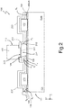
Figure 2 is a schematic cross-section view (not in scale) of the present HEMT; -
Figures 3-4 are schematic top plan views (not in scale) with portions removed of the HEMT illustrated inFigure 2 ; and -
Figures 5-14 are schematic cross-section views (not in scale) of the HEMT illustrated inFigure 2 , during successive steps of a manufacturing process. -
Figure 2 shows aHEMT 100, which is described in what follows limitedly to the differences with respect to theHEMT 1 illustrated inFigure 1 , except where otherwise specified. Moreover, elements already present in the HEMT 1 are designated by the same reference numbers, increased by 100, except where otherwise specified. The first, second, and third surfaces are once again denoted by Sa, Sb, and Sc. - In detail, and without this implying any loss of generality, the
source metallization 120 and thedrain metallization 122 traverse thetop layer 106 only partially. Consequently, thesource metallization 120 and thedrain metallization 122 overlie thebottom layer 104 at a distance therefrom. - In greater detail, each of the
source metallization 120 and thedrain metallization 122 has a respective top portion, which extends on the second surface Sb, and a respective bottom portion, which extends underneath the second surface Sb, within a top part of thetop layer 106. In addition, the passivation region (designated by 108), referred to in what follows as the firstdielectric layer 108, coats at the top and laterally the top portions of thesource metallization 120 and of thedrain metallization 122, in addition to thetop layer 106. - The first
dielectric layer 108 defines the first surface Sa, which is parallel to the plane xy and delimits at the top the part of the firstdielectric layer 108 laterally staggered with respect to thesource metallization 120 and to thedrain metallization 122, this part being plane. - The HEMT 100 further comprises a
first opening 109, which extends through the firstdielectric layer 108, and in particular the aforementioned plane part of the firstdielectric layer 108, giving out onto thetop layer 106. Thefirst opening 109 is hence delimited laterally by the firstdielectric layer 108 and may have a substantially parallelepipedal shape. In this case, in top plan view, thefirst opening 109 has a rectangular shape. In this connection, to indicate the ensemble of the four edges of the firstdielectric layer 108, which delimit the section of thefirst opening 109 in the plane of the first surface Sa, will be referred to in what follows as thebroken line 199. Thebroken line 199 hence lies in the plane of the first surface Sa and has a closed, rectangular, shape. - Without this implying any loss of generality, the
gate region 110 is equidistant from thesource metallization 120 and from thedrain metallization 122. - The
gate region 110 comprises abottom region 211, made of nickel. - The
bottom region 211 includes arespective bottom portion 212, which occupies thefirst opening 109 and hence extends underneath the first surface Sa, contacting thetop layer 106. Moreover, thebottom region 211 comprises a respectivetop portion 213, which extends on the first surface Sa so as to overlie thebottom portion 212. - The
top portion 213 of thebottom region 211 comprises parts laterally staggered with respect to thefirst opening 109 so that the section of the first opening 109 in the plane of the first surface Sa is entirely overlaid by thetop portion 213. In particular, as illustrated inFigure 3 (where for simplicity of representation just thetop portion 213 and thefirst opening 109 are shown), thebroken line 199, which forms the perimeter of the entrance of thefirst opening 109, is entirely overlaid by thetop portion 213 of thebottom region 211, which to a first approximation has, for example, a parallelepipedal shape. In fact, thetop portion 213 projects laterally, towards the outside, beyond the entire perimeter of the entrance of thefirst opening 109, defined precisely by thebroken line 109. Equivalently, in top plan view, thebroken line 199 is entirely contained within thetop portion 213 of thebottom region 211 of thegate region 110. - In other words, by designating with P1, P2, P3, P4 the side walls of the parallelepiped shape of the abovementioned
top portion 213, each of these walls substantially extends in a way perpendicular to the first surface Sa, on top of a corresponding portion of the firstdielectric layer 108. The walls P1-P4 are thus perpendicular also to the second surface Sb, which represents the front surface of the semiconductor body. - In particular, each of the walls P1-P4 forms, together with the underlying corresponding portion of the first
dielectric layer 108, an edge, which is arranged under the metallic material which forms thetop portion 213 and overlies the dielectric material which forms the firstdielectric layer 108. - Referring, as an example, to the wall P1, it forms an edge E1 with the first
dielectric layer 108. Therefore, by designating with E2 the edge formed by thefirst opening 109 with thetop layer 106, parallel to the edge E1 and close to this latter, i.e., the edge formed by thebottom portion 212, the firstdielectric layer 108 and thetop layer 106, the following occurs. - When the
HEMT transistor 100 is off, i.e., when a negative voltage is applied on thegate region 110, when the (positive) voltage on thedrain metallization 122 rises, initially a raise of the electric field in proximity of the edge E2 occurs, as long as the voltage on thedrain metallization 122 does not overcome a threshold; after the voltage on thedrain metallization 122 overcomes the threshold, the electric field starts to distribute also in proximity of the edge E1. Therefore, above the threshold, the electric field in proximity to the edge E2, i.e., in the zone with a higher risk of breakdown, is reduced. - Without this implying any loss of generality, the
bottom region 211 of thegate region 110 has a thickness comprised between 30 nm and 200 nm. - The
HEMT 100 further comprises asecond dielectric layer 220, which is made of the same material as that of thefirst dielectric layer 108. Thesecond dielectric layer 220 may hence be made, for example, of silicon nitride. Moreover, thesecond dielectric layer 220 overlies, in direct contact, thefirst dielectric layer 108. - A
second opening 229 extends through thesecond dielectric layer 220, so as to expose a part of thetop portion 213 of thebottom region 211 of thegate region 110. In practice, thesecond dielectric layer 220 coats at the top and laterally a peripheral portion of thetop portion 213, leaving a central part of thetop portion 213 exposed. Moreover, the first and seconddielectric layers top layer 106 form a package that encapsulates thebottom region 211 of thegate region 110; thesecond opening 229 passes through this package. - The
gate region 110 further comprises anintermediate region 311, which is made, for example, of tungsten nitride (WN) or else tantalum nitride (TaN) and has a thickness comprised, for example, between 40 nm and 100 nm. Moreover, thegate region 110 comprises at least onetop region 411, which is made, for example, of aluminium, overlies theintermediate region 311, and has a thickness comprised, for example, between 300 nm and 700 nm. - In detail, the
intermediate region 311 extends into thesecond opening 229 so as to coat the side walls and the bottom of thesecond opening 229, contacting thetop portion 213 of thebottom region 211 of thegate region 110. In addition, as illustrated also inFigure 4 (where for simplicity of representation only theintermediate region 311, thesecond dielectric layer 220, thesecond opening 229, thetop portion 213, and the first opening 109), and without this implying any loss of generality, theintermediate region 311 also extends on portions of thesecond dielectric layer 220 that laterally delimit thesecond opening 229. In practice, theintermediate region 311 closes the aforementioned package. - For practical purposes, the
bottom portion 212 of thebottom region 211 of thegate region 110 forms a Schottky contact with thetop layer 106. Thetop region 411 of thegate region 110 functions as low-resistance region. In fact, it is made of a low-resistivity metal material (aluminium), which is commonly used in numerous technological processes (e.g., in the lines for manufacturing CMOS circuits) without generating contamination, unlike what occurs, for example, in the case of gold. Theintermediate region 311 functions, instead, as barrier layer, which prevents the aluminium that forms thetop region 411 from diffusing, through thebottom region 211, as far as into contact with thetop layer 106, in particular in the presence of temperatures higher than 300°C; were it to occur, the above diffusion of the aluminium into thetop layer 106 would lead to damage to the Schottky junction on account of the relatively low value of the work function of aluminium. - The
HEMT 100 may be manufactured, for example, with the manufacturing process described in what follows. - Initially, as illustrated in
Figure 5 , formed in a way in itself known are thesemiconductor body 102, thesource metallization 120, thedrain metallization 122, and thefirst dielectric layer 108, the latter coating entirely thetop layer 106 in so far as it is without thefirst opening 109. - Next, as illustrated in
Figure 6 , a portion of thefirst dielectric layer 108 is selectively removed, for example by means of a dry etch, so as to form thefirst opening 109, which gives out onto thetop layer 106. - Then, as illustrated in
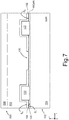
Figure 7 , atemporary structure 500 is formed, which includes a firsttemporary layer 502 and a secondtemporary layer 504. - In detail, the first
temporary layer 502 extends on thefirst dielectric layer 108 and fills thefirst opening 109 entirely. The secondtemporary layer 504 extends on the firsttemporary layer 502. - In greater detail, the first
temporary layer 502 is formed by a non-photosensitive resist (e.g., a non-photosensitive organic material), whereas the secondtemporary layer 504 is formed by a photosensitive resist, so that thetemporary structure 500 forms a so-called "bilayer", where the firsttemporary layer 502 forms the so-called "underlayer". - Next, in a way in itself known, a portion of the second temporary layer 504 (step not illustrated) is exposed to radiation, and then a chemical etch is carried out so as to obtain what is illustrated in
Figure 8 . - In detail, a
main cavity 510 is formed, which extends through the first and secondtemporary layers main cavity 510 is formed by a throughcavity 514, which traverses the secondtemporary layer 504, and by anunderlying recess 512, which communicates with the overlying throughcavity 514 and extends through the firsttemporary layer 502 in a way such as to expose a portion of thefirst dielectric layer 108, which delimits thefirst opening 109. - To a first approximation, both the through
cavity 514 and therecess 512 are parallelepipedal. Moreover, therecess 512 communicates with thefirst opening 109. To a first approximation, thefirst opening 109, therecess 512, and the throughcavity 514 are vertically aligned. Once again to a first approximation, the section of therecess 512 perpendicular to the axis z has dimensions along the axis x and the axis y greater than the corresponding dimensions of the section of the throughcavity 514. Moreover, the section of thefirst opening 109 perpendicular to the axis z has dimensions along the axis x and the axis y smaller than the corresponding dimensions of the section of the throughcavity 514. - In practice, the
first opening 109 is entirely overlaid, at a distance, by the throughcavity 514. In addition, part of the secondtemporary layer 504 extends in cantilever fashion; i.e., it projects, over therecess 512, so as to form a restriction. Equivalently, at the transition between first and secondtemporary layers 502, 406, themain cavity 510 has a section, perpendicular to the axis z, that widens from the top downwards. - Next, as illustrated in
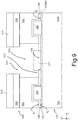
Figure 9 , formed by physical vapour deposition (PVD) is thebottom region 211 of thegate region 110, which extends not only in thefirst opening 109, but also on part of the bottom of therecess 512, at a distance from the firsttemporary layer 502, as well as underneath the throughcavity 514, hence without penetrating into the latter or contacting the secondtemporary layer 504. This operation likewise involves formation of atemporary nickel region 515, which extends on the secondtemporary layer 504 and is physically separate from thebottom region 211 of thegate region 110, as a result of the shape of themain cavity 510. - Next, there are performed a lift-off process in order to remove the
temporary region 515, and a subsequent operation of removal of thetemporary structure 500, so as to obtain what is illustrated inFigure 10 . Lift-off can take place thanks to the fact that thetemporary region 515 is separate from the underlyingbottom region 211 of thegate region 110. - Then, as illustrated in
Figure 11 , thesecond dielectric layer 220 is formed, for example by PECVD. Thesecond dielectric layer 220 extends ovn thefirst dielectric layer 108 and on thebottom region 211 of thegate region 110. In particular, thesecond dielectric layer 220 coats at the top and laterally thetop portion 213 of thebottom region 211 of thegate region 110. - Next, a dry etch is carried out so as to remove selectively a portion of the
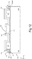
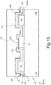
second dielectric layer 220 arranged on thebottom region 211 of thegate region 110, so as to form thesecond opening 229, as illustrated inFigure 12 . - Then, two sputtering processes are carried out in succession, as illustrated in
Figure 13 . In particular, a first process of sputtering of tungsten nitride (WN) or else of tantalum nitride (TaN) enables formation of alayer 1311, referred to in what follows as thefirst metal layer 1311; a subsequent second process of sputtering of aluminium enables formation of alayer 1411, referred to in what follows as thesecond metal layer 1411. - The
first metal layer 1311 extends on thesecond dielectric layer 220 and coats the side walls and the bottom of thesecond opening 229. Thesecond metal layer 1411 extends on thefirst metal layer 1311. - Next, portions of the
second metal layer 1411, as well as underlying portions of thefirst metal layer 1311, are selectively removed via the use of a resistmask 1500, which is arranged on thesecond metal layer 1411. As illustrated inFigure 14 , the remaining portions of the first andsecond metal layers intermediate region 311 and thetop region 411 of thegate region 110, respectively. - Then, in a way not illustrated, the resist
mask 1500 is removed. - From what has been described and illustrated previously above, the advantages that the present solution affords emerge clearly.
- In particular, the present HEMT has a gate region in which the low-resistivity subportion is made of a material that can be used on the most common lines for manufacturing integrated circuits, without giving rise to major contamination, hence without contaminating, for example, the manufacturing equipment. Moreover, even though this material may present a not particularly high work function, it does not involve risks of damage to the Schottky junction, thanks to the presence of the barrier layer.
- In conclusion, it is clear that modifications and variations may be made to what has been described and illustrated herein, without thereby departing from the sphere of protection of the present invention, as defined in the annexed claims.
- For instance, the
gate region 110 may include, on thetop region 411, an additional metal region (not illustrated), made, for example, of titanium nitride and having the function of anti-reflection layer. - The additional metal region may be formed by carrying out a respective sputtering step, prior to execution of the etch illustrated in
Figure 14 , said sputtering causing formation of a third metal layer (not illustrated) on thesecond metal layer 1411. In this case, the resistmask 1500 is then arranged on the third metal layer. - More in general, the
gate region 110 may have further layers additional to the ones described. - The
source metallization 120 and thedrain metallization 122 may have shapes and arrangements different from what has been described. For instance, thesource metallization 120 and thedrain metallization 122 may penetrate in part into thebottom layer 104, or else may be arranged entirely on thetop layer 106, albeit in contact with the latter. - The structure of the
semiconductor body 102 may be different from what has been described. - For instance, the
bottom layer 104 may include a respective top portion and a respective bottom portion (not illustrated), which are doped, for example, with carbon atoms. In this case, the top portion is doped with carbon atoms to a lesser extent than the bottom portion and functions as so-called channel layer, whereas the bottom portion of thebottom layer 104 functions as buffer layer. - Between the
bottom layer 104 and thetop layer 106 there may be present a spacer layer (not illustrated), made, for example, of aluminium nitride and having a small thickness, for example of 1 nm; the spacer layer serves to improve the mobility of the 2-dimensional electron gas. - Doping of the
semiconductor body 102 may be of a type different from what has been described. For instance, thebottom layer 104 and thetop layer 106 may be of a P type. - The HEMT may include passivation regions different from what has been described. Moreover, the present HEMT may be indifferently of the normally ON or normally OFF channel type.
- The openings and the recesses may have shapes different from what has been described. For instance, the
first opening 109, the throughcavity 514, and therecess 512 may have sections of a circular shape, in which case thebroken line 199 is replaced by a circular profile. - In addition, the
bottom region 211, theintermediate region 311, and thetop region 411 of thegate region 110 may be made of materials different from what has been described. For instance, theintermediate region 311 may be made of titanium-titanium oxynitride-titanium (TiTiONTi), instead of tantalum or tungsten nitride. - As regards, the manufacturing process, the
main cavity 510 may have a shape different from the one described and/or may be formed in a different way. For instance, it is possible to use a so-called negative resist, instead of thetemporary structure 500. In this case, the main cavity has an approximately flared shape, with section that widens from the top downwards. - Finally, the manufacturing process may be such that the
bottom region 211 penetrates at least in part into thetop layer 106. For this purpose, it is possible to add a dedicated etching step, after formation of thefirst opening 109.
Claims (10)
- A HEMT transistor including a semiconductor body (102), which forms a semiconductor heterostructure (104,106) delimited by a front surface (Sb), and a conductive gate region (110), which comprises:- a contact region (211), which is made of a first metal material and contacts the semiconductor body, thereby forming a Schottky junction;- a barrier region (311), which is made of a second metal material and is arranged on the contact region; and- a top region (411), which extends on the barrier region and is made of a third metal material, which has a resistivity lower than the resistivity of the first metal material;said transistor further comprising a dielectric region (108, 220), which includes at least one front dielectric subregion (220), which extends on the contact region, delimiting a front opening (229) that gives out onto the contact region; and wherein the barrier region extends into the front opening and on at least part of said front dielectric subregion, the barrier region being configured to prevent the diffusion of the third metal material through the contact region; and wherein the dielectric region further comprises a bottom dielectric subregion (108), which extends on the semiconductor body so as to delimit a bottom opening (109); and wherein the contact region comprises:- a bottom portion (212), which extends into the bottom opening and contacts the semiconductor body; and- a top portion (213), which extends on said bottom portion and on part of the bottom dielectric subregion;and wherein said top portion is delimited, laterally, by four side walls (P1-P4), each of which extends substantially in a way perpendicular to said front surface (Sb), on top of a corresponding portion of the bottom dielectric subregion (108).
- The transistor according to claim 1, wherein the third metal material has a work function lower than the work function of the first metal material.
- The transistor according to any one of the preceding claims, wherein said first and third metal materials are nickel and aluminium, respectively; and wherein said second metal material is a metal alloy containing nitrogen.
- The transistor according to any one of the preceding claims, wherein the semiconductor body (102) includes at least one surface layer (106), which is made of aluminium gallium nitride (AlGaN), and an inner layer (104), which is made of gallium nitride (GaN).
- A process for manufacturing a HEMT transistor, comprising the steps of:- forming a semiconductor body (102) in a manner such that the semiconductor body forms a semiconductor heterostructure (104,106) delimited by a front surface (Sb); and- forming a conductive gate region (110);and wherein the step of forming a conductive gate region comprises the steps of:- forming a contact region (211) made of a first metal material, which contacts the semiconductor body, thereby forming a Schottky junction;- on the contact region, forming a barrier region (311) made of a second metal material; and- on the barrier region, forming a top region (411) made of a third metal material, which has a resistivity lower than the resistivity of the first metal material;said process further comprising the step of forming, on the contact region, a front dielectric subregion (220) so that it will delimit a front opening (229) that gives out onto the contact region; and wherein the step of forming the barrier region is such that the barrier region extends into the front opening and on at least part of the front dielectric subregion, so as to prevent the diffusion of the thrd metal material through the contact region; said process further comprising the step of forming a bottom dielectric subregion (108) in a manner such that it extends on the semiconductor body and delimits a bottom opening (109); and wherein said step of forming a contact region (211) comprises:- forming a bottom portion (212) in a manner such that it extends into the bottom opening and contacts the semiconductor body; and- forming a top portion (213) in a manner such that it extends on said bottom portion and on part of the bottom dielectric subregion and is delimited, laterally, by four side walls (P1-P4), each of which extends substantially in a way perpendicular to said front surface (Sb), on top of a corresponding portion of the bottom dielectric subregion (108) .
- The manufacturing process according to claim 5, wherein said step of forming the contact region (211) comprises carrying out a chemical vapour deposition of said first metal material; and wherein said step of forming the barrier region (311) comprises carrying out, after forming said front dielectric subregion (220) and said front opening (229), a first sputtering operation of the second metal material; and wherein said step of forming the top region (411) comprises carrying out a second sputtering operation of the third metal material.
- The manufacturing process according to claim 6, wherein said step of forming the contact region (211) comprises carrying out said chemical vapour deposition after forming said bottom opening (109), so as to form the bottom portion (212) and the top portion (213) of the contact region.
- The manufacturing process according to claim 7, wherein the bottom dielectric subregion (108) and the front dielectric subregion (220) are made of silicon nitride.
- The manufacturing process according to claim 7 or claim 8, wherein said step of forming the contact region (211) comprises the steps of:- after forming the bottom dielectric subregion (108) and the bottom opening (109), and prior to forming the front dielectric subregion (220), forming on the bottom dielectric subregion and the bottom opening a temporary dielectric structure (500), which laterally delimits a cavity (510) that overlies the bottom opening;- after forming said cavity (510), carrying out said chemical vapour deposition, thereby forming the contact region (211) and an additional region (515), which extends on the temporary dielectric structure, is made of the first metal material and is separate from the contact region; and then- removing the additional region and the temporary dielectric structure; and then- carrying out the step of forming the front dielectric subregion.
- The manufacturing process according to claim 9, wherein at least part of said cavity (510) has a section that widens in the direction of the semiconductor body (102); and wherein said step of removing the temporary dielectric structure (515) is carried out by means of lift-off.
Applications Claiming Priority (1)
| Application Number | Priority Date | Filing Date | Title |
|---|---|---|---|
| IT102018000011065A IT201800011065A1 (en) | 2018-12-13 | 2018-12-13 | HEMT TRANSISTOR INCLUDING A PERFECTED PORT REGION AND RELATED MANUFACTURING PROCESS |
Publications (1)
| Publication Number | Publication Date |
|---|---|
| EP3667735A1 true EP3667735A1 (en) | 2020-06-17 |
Family
ID=65685908
Family Applications (1)
| Application Number | Title | Priority Date | Filing Date |
|---|---|---|---|
| EP19216255.0A Ceased EP3667735A1 (en) | 2018-12-13 | 2019-12-13 | Hemt including a gate region and related manufacturing process |
Country Status (4)
| Country | Link |
|---|---|
| US (2) | US11799025B2 (en) |
| EP (1) | EP3667735A1 (en) |
| CN (2) | CN111326574B (en) |
| IT (1) | IT201800011065A1 (en) |
Cited By (1)
| Publication number | Priority date | Publication date | Assignee | Title |
|---|---|---|---|---|
| EP3836228A1 (en) | 2019-12-10 | 2021-06-16 | STMicroelectronics S.r.l. | Hemt transistor including field plate regions and manufacturing process thereof |
Families Citing this family (4)
| Publication number | Priority date | Publication date | Assignee | Title |
|---|---|---|---|---|
| US12112983B2 (en) | 2020-08-26 | 2024-10-08 | Macom Technology Solutions Holdings, Inc. | Atomic layer deposition of barrier metal layer for electrode of gallium nitride material device |
| US12408365B2 (en) * | 2022-11-28 | 2025-09-02 | Nxp Usa, Inc. | Heterostructure transistor gate with diffusion barrier |
| IT202300004566A1 (en) * | 2023-03-10 | 2024-09-10 | St Microelectronics Int Nv | HEMT DEVICE WITH REDUCED IGNITION RESISTANCE AND RELATED MANUFACTURING PROCEDURE |
| EP4471869A1 (en) * | 2023-05-31 | 2024-12-04 | STMicroelectronics International N.V. | Hemt device having an improved conductivity and manufacturing process thereof |
Citations (7)
| Publication number | Priority date | Publication date | Assignee | Title |
|---|---|---|---|---|
| JP2011238805A (en) | 2010-05-11 | 2011-11-24 | Nec Corp | Field effect transistor, method of manufacturing field effect transistor and electronic device |
| US20130248873A1 (en) | 2012-03-26 | 2013-09-26 | Kabushiki Kaisha Toshiba | Nitride semiconductor device and method for manufacturing same |
| US20140092636A1 (en) * | 2012-09-28 | 2014-04-03 | Fujitsu Semiconductor Limited | Compound semiconductor device and method of manufacturing the same |
| US20150162424A1 (en) * | 2013-12-06 | 2015-06-11 | International Re'ctifier Corporation | Dual-Gated Group III-V Merged Transistor |
| US20170294530A1 (en) * | 2016-04-07 | 2017-10-12 | Semiconductor Components Industries, Llc | Electronic device including a hemt with a segmented gate electrode and a process of forming the same |
| US20180240754A1 (en) * | 2017-02-21 | 2018-08-23 | Raytheon Company | Nitride structure having gold-free contact and methods for forming such structures |
| EP3836228A1 (en) * | 2019-12-10 | 2021-06-16 | STMicroelectronics S.r.l. | Hemt transistor including field plate regions and manufacturing process thereof |
Family Cites Families (14)
| Publication number | Priority date | Publication date | Assignee | Title |
|---|---|---|---|---|
| JP3610951B2 (en) | 2002-01-16 | 2005-01-19 | ソニー株式会社 | Semiconductor device and manufacturing method of semiconductor device |
| JP4221697B2 (en) * | 2002-06-17 | 2009-02-12 | 日本電気株式会社 | Semiconductor device |
| US8319310B2 (en) | 2009-03-31 | 2012-11-27 | Freescale Semiconductor, Inc. | Field effect transistor gate process and structure |
| US8896122B2 (en) * | 2010-05-12 | 2014-11-25 | Cree, Inc. | Semiconductor devices having gates including oxidized nickel |
| CN103329273B (en) * | 2011-01-17 | 2016-03-09 | 富士通株式会社 | Semiconductor device and manufacture method thereof |
| JP5966301B2 (en) * | 2011-09-29 | 2016-08-10 | 富士通株式会社 | Compound semiconductor device and manufacturing method thereof |
| JP6025242B2 (en) * | 2012-03-30 | 2016-11-16 | 住友電工デバイス・イノベーション株式会社 | Manufacturing method of semiconductor device |
| EP2667415B1 (en) | 2012-05-22 | 2021-02-17 | Nexperia B.V. | Heterojunction semiconductor device and manufacturing method |
| JP2012216877A (en) | 2012-08-09 | 2012-11-08 | Cree Inc | Metallized structure for high electric power microelectronic device |
| US8895992B2 (en) | 2013-02-22 | 2014-11-25 | Taiwan Semiconductor Manufacturing Company, Ltd. | High electron mobility transistor and method of forming the same |
| CN103219239B (en) * | 2013-03-27 | 2015-05-27 | 中国电子科技集团公司第五十五研究所 | Method for manufacturing AlGaN/GaN HEMT (High Electron Mobility Transistor) with high thermal stability |
| US9443969B2 (en) | 2013-07-23 | 2016-09-13 | Taiwan Semiconductor Manufacturing Company, Ltd. | Transistor having metal diffusion barrier |
| ITUB20155536A1 (en) | 2015-11-12 | 2017-05-12 | St Microelectronics Srl | NORMALLY OFF TYPE HEMT TRANSISTOR INCLUDING A TRINCE CONTAINING A REGION OF GATE AND FORMER AT LEAST ONE STEP, AND ITS PROCESS OF MANUFACTURE |
| JP6724685B2 (en) * | 2016-09-23 | 2020-07-15 | 住友電気工業株式会社 | Semiconductor device |
-
2018
- 2018-12-13 IT IT102018000011065A patent/IT201800011065A1/en unknown
-
2019
- 2019-12-06 US US16/706,539 patent/US11799025B2/en active Active
- 2019-12-11 CN CN201911267996.1A patent/CN111326574B/en active Active
- 2019-12-11 CN CN201922213501.9U patent/CN211182213U/en active Active
- 2019-12-13 EP EP19216255.0A patent/EP3667735A1/en not_active Ceased
-
2023
- 2023-09-28 US US18/477,372 patent/US12278283B2/en active Active
Patent Citations (7)
| Publication number | Priority date | Publication date | Assignee | Title |
|---|---|---|---|---|
| JP2011238805A (en) | 2010-05-11 | 2011-11-24 | Nec Corp | Field effect transistor, method of manufacturing field effect transistor and electronic device |
| US20130248873A1 (en) | 2012-03-26 | 2013-09-26 | Kabushiki Kaisha Toshiba | Nitride semiconductor device and method for manufacturing same |
| US20140092636A1 (en) * | 2012-09-28 | 2014-04-03 | Fujitsu Semiconductor Limited | Compound semiconductor device and method of manufacturing the same |
| US20150162424A1 (en) * | 2013-12-06 | 2015-06-11 | International Re'ctifier Corporation | Dual-Gated Group III-V Merged Transistor |
| US20170294530A1 (en) * | 2016-04-07 | 2017-10-12 | Semiconductor Components Industries, Llc | Electronic device including a hemt with a segmented gate electrode and a process of forming the same |
| US20180240754A1 (en) * | 2017-02-21 | 2018-08-23 | Raytheon Company | Nitride structure having gold-free contact and methods for forming such structures |
| EP3836228A1 (en) * | 2019-12-10 | 2021-06-16 | STMicroelectronics S.r.l. | Hemt transistor including field plate regions and manufacturing process thereof |
Cited By (1)
| Publication number | Priority date | Publication date | Assignee | Title |
|---|---|---|---|---|
| EP3836228A1 (en) | 2019-12-10 | 2021-06-16 | STMicroelectronics S.r.l. | Hemt transistor including field plate regions and manufacturing process thereof |
Also Published As
| Publication number | Publication date |
|---|---|
| US20200194579A1 (en) | 2020-06-18 |
| CN111326574A (en) | 2020-06-23 |
| CN211182213U (en) | 2020-08-04 |
| US20240021718A1 (en) | 2024-01-18 |
| US11799025B2 (en) | 2023-10-24 |
| CN111326574B (en) | 2023-08-25 |
| US12278283B2 (en) | 2025-04-15 |
| IT201800011065A1 (en) | 2020-06-13 |
Similar Documents
| Publication | Publication Date | Title |
|---|---|---|
| US12278283B2 (en) | HEMT transistor including an improved gate region and related manufacturing process | |
| KR102488191B1 (en) | Nitride structure with low capacitance gate contact integrated with copper damascene structure | |
| CN111223865B (en) | Method for forming contact-to-gate monitoring pattern and semiconductor element | |
| US20200350399A1 (en) | Semiconductor device and fabrication method thereof | |
| US11101363B2 (en) | HEMT transistor of the normally off type including a trench containing a gate region and forming at least one step, and corresponding manufacturing method | |
| US7632726B2 (en) | Method for fabricating a nitride FET including passivation layers | |
| US9378965B2 (en) | Highly conductive source/drain contacts in III-nitride transistors | |
| TW201618276A (en) | Improved GaN structure | |
| KR101689137B1 (en) | Monolithic integrated circuit(mmic) structure and method for forming such structure | |
| US12100757B2 (en) | Cap structure coupled to source to reduce saturation current in HEMT device | |
| US9478652B1 (en) | Monolithic integrated circuit (MMIC) structure having composite etch stop layer and method for forming such structure | |
| US20250095998A1 (en) | Method for manufacturing a gate terminal of a hemt device, and hemt device | |
| US9917187B2 (en) | Semiconductor device and manufacturing method | |
| US10062630B2 (en) | Water and ion barrier for the periphery of III-V semiconductor dies | |
| US20240258373A1 (en) | Transistor device having a gate setback from a gate dielectric | |
| US20220293515A1 (en) | Via landing on first and second barrier layers to reduce cleaning time of conductive structure | |
| US9929244B2 (en) | Semiconductor device and method for producing a semiconductor device | |
| US11127863B2 (en) | Gate structure and method for producing same | |
| US9006809B2 (en) | Multi-landing contact etching | |
| TWI708282B (en) | Fusi gated device and method of forming the same | |
| US20240339332A1 (en) | Method of manufacturing semiconductor device | |
| CN120834089A (en) | Semiconductor die and method of manufacturing a semiconductor die |
Legal Events
| Date | Code | Title | Description |
|---|---|---|---|
| PUAI | Public reference made under article 153(3) epc to a published international application that has entered the european phase |
Free format text: ORIGINAL CODE: 0009012 |
|
| STAA | Information on the status of an ep patent application or granted ep patent |
Free format text: STATUS: THE APPLICATION HAS BEEN PUBLISHED |
|
| AK | Designated contracting states |
Kind code of ref document: A1 Designated state(s): AL AT BE BG CH CY CZ DE DK EE ES FI FR GB GR HR HU IE IS IT LI LT LU LV MC MK MT NL NO PL PT RO RS SE SI SK SM TR |
|
| AX | Request for extension of the european patent |
Extension state: BA ME |
|
| STAA | Information on the status of an ep patent application or granted ep patent |
Free format text: STATUS: REQUEST FOR EXAMINATION WAS MADE |
|
| 17P | Request for examination filed |
Effective date: 20201216 |
|
| RBV | Designated contracting states (corrected) |
Designated state(s): AL AT BE BG CH CY CZ DE DK EE ES FI FR GB GR HR HU IE IS IT LI LT LU LV MC MK MT NL NO PL PT RO RS SE SI SK SM TR |
|
| STAA | Information on the status of an ep patent application or granted ep patent |
Free format text: STATUS: EXAMINATION IS IN PROGRESS |
|
| 17Q | First examination report despatched |
Effective date: 20220510 |
|
| STAA | Information on the status of an ep patent application or granted ep patent |
Free format text: STATUS: THE APPLICATION HAS BEEN REFUSED |
|
| 18R | Application refused |
Effective date: 20241014 |