EP3835777A1 - Eddy current flaw detection device and eddy current flaw detection method - Google Patents
Eddy current flaw detection device and eddy current flaw detection method Download PDFInfo
- Publication number
- EP3835777A1 EP3835777A1 EP19847490.0A EP19847490A EP3835777A1 EP 3835777 A1 EP3835777 A1 EP 3835777A1 EP 19847490 A EP19847490 A EP 19847490A EP 3835777 A1 EP3835777 A1 EP 3835777A1
- Authority
- EP
- European Patent Office
- Prior art keywords
- exciter
- detector
- eddy current
- tested object
- flaw detection
- Prior art date
- Legal status (The legal status is an assumption and is not a legal conclusion. Google has not performed a legal analysis and makes no representation as to the accuracy of the status listed.)
- Granted
Links
Images



Classifications
-
- G—PHYSICS
- G01—MEASURING; TESTING
- G01N—INVESTIGATING OR ANALYSING MATERIALS BY DETERMINING THEIR CHEMICAL OR PHYSICAL PROPERTIES
- G01N27/00—Investigating or analysing materials by the use of electric, electrochemical, or magnetic means
- G01N27/72—Investigating or analysing materials by the use of electric, electrochemical, or magnetic means by investigating magnetic variables
- G01N27/82—Investigating or analysing materials by the use of electric, electrochemical, or magnetic means by investigating magnetic variables for investigating the presence of flaws
- G01N27/90—Investigating or analysing materials by the use of electric, electrochemical, or magnetic means by investigating magnetic variables for investigating the presence of flaws using eddy currents
- G01N27/904—Investigating or analysing materials by the use of electric, electrochemical, or magnetic means by investigating magnetic variables for investigating the presence of flaws using eddy currents with two or more sensors
-
- G—PHYSICS
- G01—MEASURING; TESTING
- G01N—INVESTIGATING OR ANALYSING MATERIALS BY DETERMINING THEIR CHEMICAL OR PHYSICAL PROPERTIES
- G01N27/00—Investigating or analysing materials by the use of electric, electrochemical, or magnetic means
- G01N27/72—Investigating or analysing materials by the use of electric, electrochemical, or magnetic means by investigating magnetic variables
- G01N27/82—Investigating or analysing materials by the use of electric, electrochemical, or magnetic means by investigating magnetic variables for investigating the presence of flaws
- G01N27/90—Investigating or analysing materials by the use of electric, electrochemical, or magnetic means by investigating magnetic variables for investigating the presence of flaws using eddy currents
Definitions
- Embodiments of the present invention relate to eddy current flaw detection devices and eddy current flaw detection methods.
- alternating current from an alternating current power source is supplied to an excitation coil to induce eddy current in the vicinity of a surface of a tested object made of a metal material.
- a reactive magnetic field generated by the eddy current is detected by a detection coil. If there is a flaw in the vicinity of the tested object, the eddy current would change due to the flaw, and intensity and distribution of the reactive magnetic field generated by the eddy current would also change. Thus, the flaw can be detected.
- a complex material which is composed of a plurality of different materials in a layer structure or with fiber structure, may have a lower electric conductivity compared to metals.
- eddy current density induced in the complex material becomes low due to the low electric conductivity of the complex material.
- the magnetic flux density in the reactive magnetic field generated by the eddy current becomes low, and flaw detection sensitivity becomes low.
- Patent Document 1 Japanese Patent Application Publication Hei 9-33489
- a technique using a magnetic flux meter of a superconducting quantum interference device is known to improve flaw detection sensitivity of eddy current flaw detection under a weak magnetic field.
- improvement in flaw detection sensitivity of eddy current flaw detection under a weak magnetic field is expected owing to the high sensitivity of the SQUID magnetic flux meter to a magnetic field.
- the SQUID magnetic flux meter requires a cooling mechanism, and the device has a complex structure. Thus, the device is expensive, which is a problem to be solved.
- the complex material may have a lower electric conductivity compared to metals.
- a tested object of the eddy current flaw detection is made of a complex material, the eddy current density in the tested object is lowered and the magnetic flux density generated by the eddy current is lowered, and then, the flow detection sensitivity in the eddy current flaw detection is deteriorated.
- the device may have a complex structure and may become expensive.
- An object of the embodiments of the present invention is to enable eddy current flaw detection with a simplified and inexpensive device, with high sensitivity, even with a tested object made of a low electric conductivity material such as a complex material.
- an eddy current flaw detection device comprising: a first exciter/detector configured to induce eddy current in a tested object; a second exciter/detector disposed opposite side of the first exciter/detector sandwiching the tested object therebetween, the second exciter/detector being configured to detect a change in a reactive magnetic field generated by the eddy current.
- an eddy current flaw detection device comprising: an exciter/detector configured to induce eddy current in a tested object and to detect a change in a reactive magnetic field generated by the eddy current; a backside body made of ferromagnetic material disposed opposite side of the exciter/detector sandwiching the tested object therebetween,
- an eddy current flaw detection method comprising: a first exciter/detector disposing step of disposing a first exciter/detector near a tested object; a second exciter/detector disposing step of disposing a second exciter/detector near the tested object at an opposite side of the first exciter/detector sandwiching the tested object therebetween; an excitation step, after the first and second exciter/detector disposing steps, of inducing eddy current in the tested object by the first exciter/detector; and a detection step of detecting, by the second exciter/detector, a change of reactive magnetic field generated by the eddy current.
- an eddy current flaw detection method comprising: an exciter/detector disposing step of disposing an exciter/detector near a tested object; a backside body disposing step of disposing a backside body made of ferromagnetic material, near the tested object at an opposite side of the exciter/detector sandwiching the tested object therebetween; an excitation step, after the exciter/detector disposing step and the backside body disposing step, of inducing eddy current in the tested object by the exciter/detector; and a detection step of detecting, by the exciter/detector, a change of reactive magnetic field generated by the eddy current.
- eddy current flaw detection can be conducted with a simplified and inexpensive device, with high sensitivity, even with a tested object made of a low electric conductivity material such as a complex material.
- FIG. 1 is a schematic cross-sectional view illustrating a situation where flaw detection is conducted using an eddy current flaw detection device according to a first embodiment of the present invention.
- a tested object 11 is made of a complex material which has a lower electric conductivity compared to ordinary metals.
- the complex material may include a complex material using silicon carbide fibers, carbon fiber reinforced plastics (CFRP) or glass fiber reinforced plastics (GFRP).
- CFRP carbon fiber reinforced plastics
- GFRP glass fiber reinforced plastics
- the tested object 11 is shaped in a flat plate, and has a first flat surface 12 and a second flat surface 13 which is an opposite side of and parallel to the first flat surface 12, for example.
- a flaw (a thinner part) 14 is assumed to exist on the first flat surface 12.
- the eddy current flaw detection device has an exciter 20 as a first exciter/detector and a detector 21 as a second exciter/detector.
- Each of the exciter 20 and the detector 21 may include a helical coil, for example.
- the exciter 20 is disposed on the first flat surface 12 of the tested object 11, while the detector 21 is disposed on the second flat surface 13 of the tested object 11.
- the exciter 20 and the detector 21 are disposed so that the axis A of the coils is directed perpendicular to the first flat surface 12 and the second flat surface 13.
- the exciter 20 is connected to an alternating current power source 22.
- the detector 21 is connected to a detector circuit (not illustrated).
- Coil wire elements constituting the exciter 20 are thicker than those constituting the detector 21 in order to suppress Joule loss in the exciter 20, because larger electric current is needed to flow in the exciter 20.
- a variating magnetic field is generated around the exciter 20.
- Examples of magnetic force lines M are shown as dash lines in Fig. 1 .
- the magnetic field generated by the exciter 20 is substantially symmetrical around the axis A of the exciter 20, although magnetic force lines M on only right side are illustrated in Fig. 1 .
- the variating magnetic field is generated around the exciter 20, eddy current is induced in the tested object 11.
- the eddy current causes a reactive magnetic field to be generated.
- the reactive magnetic field is detected as a voltage by the detector 21 and the detector circuit. Since the reactive magnetic field changes because of the flaw 14, the flaw 14 can be detected as a change in the voltage by the detector circuit.
- the tested object 11 is made of an ordinary metallic material, most of the magnetic flux passes through the tested object 11 as a result of skin effect, and substantially no magnetic field exists on the back surface (the second flat surface 13) of the tested object 11.
- the tested object 11 is a stainless steel plate of 2 mm thickness and alternating current of a frequency of 500 kHz is supplied, depth of penetration with the skin effect would be about 0.7 mm.
- the tested object 11 is made of a complex material, depth of penetration of the magnetic field due to the skin effect is larger compared to that in case of ordinary metal. Therefore, the magnetic field penetrates the tested object 11, and there exists the magnetic field even on the back surface (the second flat surface 13) of the tested object 11. However, the magnetic flux density in the tested object 11 is lower than that in the tested object 11 of ordinary metal.
- the exciter 20 and the detector 21 are separated and disposed sandwiching the tested object 11 therebetween.
- the exciter 20 and the detector 21 can be disposed close to the tested object 11.
- the detector 21 can be disposed at a location where the magnetic flux density is relatively high, which results in a relatively high accuracy in the flaw detection.
- the exciter 20 and the detector 21 may not have a same structure or a same specification. They can be designed to have different coil wire element thicknesses, different numbers of turns, different shapes and different sizes, for example, to fit their respective coils.
- the coils of the exciter 20 preferably have thicker coil wire elements because relatively larger electric current is needed to flow there.
- the coils of the detector 21 preferably have thinner coil wire elements and more wire turns, because the coils of the detector 21 do not need to allow large electric current while it is preferred to have a larger voltage output to be gained.
- the tested object 11 is made of a low electric conductivity material such as a complex material
- highly sensitive flaw detection can be conducted by setting the power source with higher frequency which would result in a smaller penetration depth. Therefore, the frequency of the power source is preferably in order of MHz.
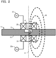
- FIG. 2 is a schematic cross-sectional view illustrating a situation where flaw detection is conducted using an eddy current flaw detection device according to a second embodiment of the present invention.
- the eddy current flaw detection device has a first exciter/detector 25 and a second exciter/detector 26.
- the first exciter/detector 25 and the second exciter/detector 26 are both helical coils, for example.
- the first exciter/detector 25 is disposed on the first flat surface 12 of the tested object 11, while the second exciter/detector 26 is disposed on the second flat surface 13 of the tested object 11.
- the first exciter/detector 25 and the second exciter/detector 26 are disposed so that the axis A of the coils is directed perpendicular to the first flat surface 12 and the second flat surface 13.
- the first exciter/detector 25 is connected to an alternating current power source 22.
- the second exciter/detector 26 is connected to another alternating current power source 22a.
- the first exciter/detector 25 and the second exciter/detector 26 are connected to respective detector circuits (not illustrated).
- the first exciter/detector 25 and the second exciter/detector 26 have substantially same structures, and each has both functions of an exciter and a detector.
- the alternating current power sources 22 and 22a may have same structures, and preferably, they have the same frequency and the same phase, synchronizing each other. Alternatively, the alternating current power sources 22 and 22a may be a single alternating current power source.
- effects of the excitation actions in the first exciter/detector 25 and the second exciter/detector 26 are combined together, and higher density of magnetic flux is obtained. Then, eddy current induced in the tested object 11 would be enhanced, which would result in a larger change in reactive magnetic flux generated by the eddy current. Then, relatively large voltage change is detected by the first exciter/detector 25 and the second exciter/detector 26 which function as detectors. In addition, still larger voltage change can be detected by adding the voltages obtained by the first exciter/detector 25 and the second exciter/detector 26 which function as detectors.
- the alternating current supplied to the first exciter/detector 25 and the second exciter/detector 26 have preferably same frequency and same phase and are synchronized with each other.
- the magnetic fields generated by the first exciter/detector 25 and the second exciter/detector 26 may be enhanced by each other in some other conditions, and flaw detection may be conducted in such other conditions where the magnetic fields are enhanced by each other.
- both the first exciter/detector 25 and the second exciter/detector 26 function as detectors, and the voltage signals detected by them are added.
- the voltage signals detected by the first exciter/detector 25 and the second exciter/detector 26 may be processed for flaw detection, by subtraction rather than addition, depending on the phase relation between the alternating currents supplied to the first exciter/detector 25 and the second exciter/detector 26.
- FIG. 3 is a schematic cross-sectional view illustrating a situation where flaw detection is conducted using an eddy current flaw detection device according to a third embodiment of the present invention.
- the third embodiment is a modification of the second embodiment.
- the outer surfaces of the first exciter/detector 25 and the second exciter/detector 26 except the parts facing the tested object 11 are covered with covers 30 made of ferromagnetic material.
- the other structures are the same as the structures of the second embodiment.
- the effects of the second embodiment are obtained.
- the magnetic field generated by supplying alternating current to the first exciter/detector 25 and the second exciter/detector 26 is distributed along the magnetic path formed in the covers 30 of ferromagnetic material, and the magnetic flux density would be enhanced.
- the magnetic flux density penetrating the flaw 14 and crossing the first exciter/detector 25 or the second exciter/detector 26 can be enhanced, which enables highly sensitive flaw detection.
- the third embodiment described above is a modification of the second embodiment, and the outer surfaces of the first exciter/detector 25 and the second exciter/detector 26 except the parts facing the tested object 11 are covered with covers 30 of ferromagnetic material.
- the outer surfaces of the exciter 20 and the detector 21 of the first embodiment except the parts facing the tested object 11 may be covered with the covers 30 of ferromagnetic material. Even in such a modified case, the magnetic flux density in the tested object 11 can be enhanced as the effect of the covers 30 of ferromagnetic material.
- FIG. 4 is a schematic cross-sectional view illustrating a situation where flaw detection is conducted using an eddy current flaw detection device according to a fourth embodiment of the present invention.
- the eddy current flaw detection device has an exciter/detector 35 and a backside body 36 made of ferromagnetic material.
- the exciter/detector 35 of this embodiment is disposed in contact with the first flat surface 12, and may have a structure similar to the structure of the first exciter/detector 25 of the second embodiment.
- the exciter/detector 35 is connected to the alternating current power source 22 and the detector circuit (not illustrated).
- the backside body 36 of ferromagnetic material is disposed opposite to the exciter/detector 35 sandwiching the tested object 11 therebetween, and in contact with the second flat surface 13.
- the backside body 36 preferably covers all part of the second surface 13 which opposes to the exciter/detector 35 sandwiching the tested object 11.
- the exciter/detector 35 has both functions of an exciter and a detector.
- alternating current is supplied from the alternating current power source 22 to the exciter/detector 35, and variating magnetic field is formed in and around the tested object 11.
- eddy current is induced in the tested object 11, and a reactive magnetic field is formed.
- the backside body 36 of ferromagnetic material the magnetic flux density in the tested object 11 is enhanced, and sensitivity of detection of the flaw 14 is enhanced.
- FIG. 5 is a schematic cross-sectional view illustrating a situation where flaw detection is conducted using an eddy current flaw detection device according to a fifth embodiment of the present invention.
- the fifth embodiment is a modification of the fourth embodiment.
- the exciter/detector 35 of the fourth embodiment is replaced with an exciter 20 and a detector 21.
- the structures of the exciter 20 and the detector 21 of the fifth embodiment may be the same as those of the exciter 20 and the detector 21 of the first embodiment.
- the exciter 20 is disposed in contact with the first flat surface 12 of the tested object 11 while the detector 21 is disposed opposite to the tested object sandwiching the exciter 20 therebetween.
- the other structures are the same as those of the fourth embodiment.
- the magnetic flux density is enhanced owing to the backside body 36, as the fourth embodiment, and sensitivity of detection of the flaw 14 is enhanced. Since the exciter 20 and the detector 21 are separated, as in the first embodiment, the exciter 20 and the detector 21 may have different structures and different specifications, and may have different designs with coil wire diameters, numbers of coil wire turns, shapes and sizes, etc., to fit respective purposes.
- FIG. 6 is a schematic cross-sectional view illustrating a situation where flaw detection is conducted using an eddy current flaw detection device according to a sixth embodiment of the present invention.
- the sixth embodiment is a modification of the fifth embodiment.
- a cover 40 made of ferromagnetic material is disposed covering the exciter 20 and the detector 21 which are structured and disposed in a similar way as in the fifth embodiment.
- the effects of the fifth embodiment are obtained, and the magnetic flux density in the tested object 11 can be further enhanced owing to the cover 40 made of ferromagnetic material. Then, sensitivity of detection of the flaw 14 can be further enhanced.
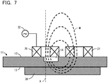
- FIG. 7 is a schematic cross-sectional view illustrating a situation where flaw detection is conducted using an eddy current flaw detection device according to a seventh embodiment of the present invention.
- the seventh embodiment is a modification of the fifth embodiment.
- the exciter 20 and the detector 21 are arranged parallel to each other both in contact with the first flat surface 12 of the tested object 11.
- the backside body 36 of ferromagnetic material is disposed opposite to the exciter 20 and the detector 21 sandwiching the tested object 11 therebetween, and in contact with the second flat surface 13.
- the backside body 36 preferably covers all part of the second surface 13 which opposes to the exciter 20 and the detector 21 sandwiching the tested object 11.
- the other structures of the seventh embodiment are same as those of the fifth embodiment.
- the magnetic flux density in the tested object 11 can be enhanced owing to the backside body 36 of ferromagnetic material. Then, sensitivity of detection of the flaw 14 can be enhanced.
- the exciter 20 and the detector 21 since the exciter 20 and the detector 21 are separated, the exciter 20 and the detector 21 may have different structures and different specifications, and may have different designs with coil wire diameters, numbers of coil wire turns, shapes and sizes, etc., to fit respective purposes.
- the cover 40 in the sixth embodiment can be added to the fourth and seventh embodiments.
- 11 tested object; 12: first flat surface; 13: second flat surface; 14: flaw (thinner part); 20: exciter (first exciter/detector); 21: detector (second exciter/detector); 22, 22a: alternating current power source; 25: first exciter/detector; 26: second exciter/detector; 30: cover; 35: exciter/detector; 36: backside body; 40: cover
Landscapes
- Chemical & Material Sciences (AREA)
- Chemical Kinetics & Catalysis (AREA)
- Electrochemistry (AREA)
- Physics & Mathematics (AREA)
- Health & Medical Sciences (AREA)
- Life Sciences & Earth Sciences (AREA)
- Analytical Chemistry (AREA)
- Biochemistry (AREA)
- General Health & Medical Sciences (AREA)
- General Physics & Mathematics (AREA)
- Immunology (AREA)
- Pathology (AREA)
- Investigating Or Analyzing Materials By The Use Of Magnetic Means (AREA)
Abstract
Description
- Embodiments of the present invention relate to eddy current flaw detection devices and eddy current flaw detection methods.
- Generally, in eddy current detection, alternating current from an alternating current power source is supplied to an excitation coil to induce eddy current in the vicinity of a surface of a tested object made of a metal material. A reactive magnetic field generated by the eddy current is detected by a detection coil. If there is a flaw in the vicinity of the tested object, the eddy current would change due to the flaw, and intensity and distribution of the reactive magnetic field generated by the eddy current would also change. Thus, the flaw can be detected.
- A complex material, which is composed of a plurality of different materials in a layer structure or with fiber structure, may have a lower electric conductivity compared to metals. When a tested object is made of a complex material in an eddy current flaw detection, eddy current density induced in the complex material becomes low due to the low electric conductivity of the complex material. Thus, the magnetic flux density in the reactive magnetic field generated by the eddy current becomes low, and flaw detection sensitivity becomes low.
- Patent Document 1: Japanese Patent Application Publication
Hei 9-33489 - A technique using a magnetic flux meter of a superconducting quantum interference device (SQUID) is known to improve flaw detection sensitivity of eddy current flaw detection under a weak magnetic field. With such a technique, improvement in flaw detection sensitivity of eddy current flaw detection under a weak magnetic field is expected owing to the high sensitivity of the SQUID magnetic flux meter to a magnetic field. However, the SQUID magnetic flux meter requires a cooling mechanism, and the device has a complex structure. Thus, the device is expensive, which is a problem to be solved.
- The complex material may have a lower electric conductivity compared to metals. When a tested object of the eddy current flaw detection is made of a complex material, the eddy current density in the tested object is lowered and the magnetic flux density generated by the eddy current is lowered, and then, the flow detection sensitivity in the eddy current flaw detection is deteriorated. On the other hand, if a highly sensitive magnetic detector is used as a detector for eddy current flaw detection, the device may have a complex structure and may become expensive.
- An object of the embodiments of the present invention is to enable eddy current flaw detection with a simplified and inexpensive device, with high sensitivity, even with a tested object made of a low electric conductivity material such as a complex material.
- In order to solve the problems, according to an embodiment, there is presented an eddy current flaw detection device comprising: a first exciter/detector configured to induce eddy current in a tested object; a second exciter/detector disposed opposite side of the first exciter/detector sandwiching the tested object therebetween, the second exciter/detector being configured to detect a change in a reactive magnetic field generated by the eddy current.
- According to another embodiment, there is presented an eddy current flaw detection device comprising: an exciter/detector configured to induce eddy current in a tested object and to detect a change in a reactive magnetic field generated by the eddy current; a backside body made of ferromagnetic material disposed opposite side of the exciter/detector sandwiching the tested object therebetween,
- According to yet another embodiment, there is presented an eddy current flaw detection method comprising: a first exciter/detector disposing step of disposing a first exciter/detector near a tested object; a second exciter/detector disposing step of disposing a second exciter/detector near the tested object at an opposite side of the first exciter/detector sandwiching the tested object therebetween; an excitation step, after the first and second exciter/detector disposing steps, of inducing eddy current in the tested object by the first exciter/detector; and a detection step of detecting, by the second exciter/detector, a change of reactive magnetic field generated by the eddy current.
- According to yet another embodiment, there is presented an eddy current flaw detection method comprising: an exciter/detector disposing step of disposing an exciter/detector near a tested object; a backside body disposing step of disposing a backside body made of ferromagnetic material, near the tested object at an opposite side of the exciter/detector sandwiching the tested object therebetween; an excitation step, after the exciter/detector disposing step and the backside body disposing step, of inducing eddy current in the tested object by the exciter/detector; and a detection step of detecting, by the exciter/detector, a change of reactive magnetic field generated by the eddy current.
- According to the embodiments of the present invention, eddy current flaw detection can be conducted with a simplified and inexpensive device, with high sensitivity, even with a tested object made of a low electric conductivity material such as a complex material.
-
-
FIG. 1 is a schematic cross-sectional view illustrating a situation where flaw detection is conducted using an eddy current flaw detection device according to a first embodiment of the present invention. -
FIG. 2 is a schematic cross-sectional view illustrating a situation where flaw detection is conducted using an eddy current flaw detection device according to a second embodiment of the present invention. -
FIG. 3 is a schematic cross-sectional view illustrating a situation where flaw detection is conducted using an eddy current flaw detection device according to a third embodiment of the present invention. -
FIG. 4 is a schematic cross-sectional view illustrating a situation where flaw detection is conducted using an eddy current flaw detection device according to a fourth embodiment of the present invention. -
FIG. 5 is a schematic cross-sectional view illustrating a situation where flaw detection is conducted using an eddy current flaw detection device according to a fifth embodiment of the present invention. -
FIG. 6 is a schematic cross-sectional view illustrating a situation where flaw detection is conducted using an eddy current flaw detection device according to a sixth embodiment of the present invention. -
FIG. 7 is a schematic cross-sectional view illustrating a situation where flaw detection is conducted using an eddy current flaw detection device according to a seventh embodiment of the present invention. - Hereinafter, eddy current flaw detection devices and eddy current flaw detection methods according to embodiments of the present invention will be described with reference to the drawings. In the following description, same or similar parts are assigned common references, and repetitive explanation will be omitted.
-
FIG. 1 is a schematic cross-sectional view illustrating a situation where flaw detection is conducted using an eddy current flaw detection device according to a first embodiment of the present invention. - In the first embodiment, a tested
object 11 is made of a complex material which has a lower electric conductivity compared to ordinary metals. The complex material may include a complex material using silicon carbide fibers, carbon fiber reinforced plastics (CFRP) or glass fiber reinforced plastics (GFRP). The testedobject 11 is shaped in a flat plate, and has a firstflat surface 12 and a secondflat surface 13 which is an opposite side of and parallel to the firstflat surface 12, for example. A flaw (a thinner part) 14 is assumed to exist on the firstflat surface 12. - The eddy current flaw detection device according to the first embodiment has an
exciter 20 as a first exciter/detector and adetector 21 as a second exciter/detector. Each of theexciter 20 and thedetector 21 may include a helical coil, for example. Theexciter 20 is disposed on the firstflat surface 12 of the testedobject 11, while thedetector 21 is disposed on the secondflat surface 13 of the testedobject 11. Theexciter 20 and thedetector 21 are disposed so that the axis A of the coils is directed perpendicular to the firstflat surface 12 and the secondflat surface 13. Theexciter 20 is connected to an alternatingcurrent power source 22. Thedetector 21 is connected to a detector circuit (not illustrated). - Coil wire elements constituting the
exciter 20 are thicker than those constituting thedetector 21 in order to suppress Joule loss in theexciter 20, because larger electric current is needed to flow in theexciter 20. - When alternating current is supplied from the alternating
current power source 22 to theexciter 20, a variating magnetic field is generated around theexciter 20. Examples of magnetic force lines M are shown as dash lines inFig. 1 . The magnetic field generated by theexciter 20 is substantially symmetrical around the axis A of theexciter 20, although magnetic force lines M on only right side are illustrated inFig. 1 . - Since the variating magnetic field is generated around the
exciter 20, eddy current is induced in the testedobject 11. The eddy current causes a reactive magnetic field to be generated. The reactive magnetic field is detected as a voltage by thedetector 21 and the detector circuit. Since the reactive magnetic field changes because of theflaw 14, theflaw 14 can be detected as a change in the voltage by the detector circuit. - If the tested
object 11 is made of an ordinary metallic material, most of the magnetic flux passes through the testedobject 11 as a result of skin effect, and substantially no magnetic field exists on the back surface (the second flat surface 13) of the testedobject 11. In a case where the testedobject 11 is a stainless steel plate of 2 mm thickness and alternating current of a frequency of 500 kHz is supplied, depth of penetration with the skin effect would be about 0.7 mm. - On the other hand, if the tested
object 11 is made of a complex material, depth of penetration of the magnetic field due to the skin effect is larger compared to that in case of ordinary metal. Therefore, the magnetic field penetrates the testedobject 11, and there exists the magnetic field even on the back surface (the second flat surface 13) of the testedobject 11. However, the magnetic flux density in the testedobject 11 is lower than that in the testedobject 11 of ordinary metal. - In the present embodiment, the
exciter 20 and thedetector 21 are separated and disposed sandwiching the testedobject 11 therebetween. Thus, theexciter 20 and thedetector 21 can be disposed close to the testedobject 11. Thus, thedetector 21 can be disposed at a location where the magnetic flux density is relatively high, which results in a relatively high accuracy in the flaw detection. - The
exciter 20 and thedetector 21 may not have a same structure or a same specification. They can be designed to have different coil wire element thicknesses, different numbers of turns, different shapes and different sizes, for example, to fit their respective coils. The coils of theexciter 20 preferably have thicker coil wire elements because relatively larger electric current is needed to flow there. On the other hand, the coils of thedetector 21 preferably have thinner coil wire elements and more wire turns, because the coils of thedetector 21 do not need to allow large electric current while it is preferred to have a larger voltage output to be gained. - When the tested
object 11 is made of a low electric conductivity material such as a complex material, highly sensitive flaw detection can be conducted by setting the power source with higher frequency which would result in a smaller penetration depth. Therefore, the frequency of the power source is preferably in order of MHz. -
FIG. 2 is a schematic cross-sectional view illustrating a situation where flaw detection is conducted using an eddy current flaw detection device according to a second embodiment of the present invention. - The eddy current flaw detection device according to the second embodiment has a first exciter/
detector 25 and a second exciter/detector 26. - The first exciter/
detector 25 and the second exciter/detector 26 are both helical coils, for example. The first exciter/detector 25 is disposed on the firstflat surface 12 of the testedobject 11, while the second exciter/detector 26 is disposed on the secondflat surface 13 of the testedobject 11. The first exciter/detector 25 and the second exciter/detector 26 are disposed so that the axis A of the coils is directed perpendicular to the firstflat surface 12 and the secondflat surface 13. The first exciter/detector 25 is connected to an alternatingcurrent power source 22. The second exciter/detector 26 is connected to another alternatingcurrent power source 22a. The first exciter/detector 25 and the second exciter/detector 26 are connected to respective detector circuits (not illustrated). - The first exciter/
detector 25 and the second exciter/detector 26 have substantially same structures, and each has both functions of an exciter and a detector. The alternatingcurrent power sources current power sources - According to the second embodiment, effects of the excitation actions in the first exciter/
detector 25 and the second exciter/detector 26 are combined together, and higher density of magnetic flux is obtained. Then, eddy current induced in the testedobject 11 would be enhanced, which would result in a larger change in reactive magnetic flux generated by the eddy current. Then, relatively large voltage change is detected by the first exciter/detector 25 and the second exciter/detector 26 which function as detectors. In addition, still larger voltage change can be detected by adding the voltages obtained by the first exciter/detector 25 and the second exciter/detector 26 which function as detectors. - In the above description, the alternating current supplied to the first exciter/
detector 25 and the second exciter/detector 26 have preferably same frequency and same phase and are synchronized with each other. However, even in cases where such a condition is not satisfied, the magnetic fields generated by the first exciter/detector 25 and the second exciter/detector 26 may be enhanced by each other in some other conditions, and flaw detection may be conducted in such other conditions where the magnetic fields are enhanced by each other. - In addition, in the above description, both the first exciter/
detector 25 and the second exciter/detector 26 function as detectors, and the voltage signals detected by them are added. However, the voltage signals detected by the first exciter/detector 25 and the second exciter/detector 26 may be processed for flaw detection, by subtraction rather than addition, depending on the phase relation between the alternating currents supplied to the first exciter/detector 25 and the second exciter/detector 26. - Further alternatively, it would be possible that only one of the first exciter/
detector 25 and the second exciter/detector 26 is used as a detector and the voltage signal from the one is used for flaw detection. -
FIG. 3 is a schematic cross-sectional view illustrating a situation where flaw detection is conducted using an eddy current flaw detection device according to a third embodiment of the present invention. - The third embodiment is a modification of the second embodiment. In the third embodiment, the outer surfaces of the first exciter/
detector 25 and the second exciter/detector 26 except the parts facing the testedobject 11 are covered withcovers 30 made of ferromagnetic material. The other structures are the same as the structures of the second embodiment. - According to the third embodiment, the effects of the second embodiment are obtained. In addition, the magnetic field generated by supplying alternating current to the first exciter/
detector 25 and the second exciter/detector 26 is distributed along the magnetic path formed in thecovers 30 of ferromagnetic material, and the magnetic flux density would be enhanced. Thus, the magnetic flux density penetrating theflaw 14 and crossing the first exciter/detector 25 or the second exciter/detector 26 can be enhanced, which enables highly sensitive flaw detection. - In the example shown in
Fig. 3 , all portions of the first exciter/detector 25 and the second exciter/detector 26 which do not face the testedobject 11 are covered with thecovers 30 of ferromagnetic material. As a modified example, alternatively, only some portions of the first exciter/detector 25 and the second exciter/detector 26 which do not face the testedobject 11 are covered with thecovers 30. Even in such a modified case, the effect of thecovers 30 of ferromagnetic material can be partially obtained. - The third embodiment described above is a modification of the second embodiment, and the outer surfaces of the first exciter/
detector 25 and the second exciter/detector 26 except the parts facing the testedobject 11 are covered withcovers 30 of ferromagnetic material. As a modification of the third embodiment, alternatively, the outer surfaces of theexciter 20 and thedetector 21 of the first embodiment except the parts facing the testedobject 11 may be covered with thecovers 30 of ferromagnetic material. Even in such a modified case, the magnetic flux density in the testedobject 11 can be enhanced as the effect of thecovers 30 of ferromagnetic material. -
FIG. 4 is a schematic cross-sectional view illustrating a situation where flaw detection is conducted using an eddy current flaw detection device according to a fourth embodiment of the present invention. - The eddy current flaw detection device according to the fourth embodiment has an exciter/
detector 35 and abackside body 36 made of ferromagnetic material. The exciter/detector 35 of this embodiment is disposed in contact with the firstflat surface 12, and may have a structure similar to the structure of the first exciter/detector 25 of the second embodiment. The exciter/detector 35 is connected to the alternatingcurrent power source 22 and the detector circuit (not illustrated). Thebackside body 36 of ferromagnetic material is disposed opposite to the exciter/detector 35 sandwiching the testedobject 11 therebetween, and in contact with the secondflat surface 13. Thebackside body 36 preferably covers all part of thesecond surface 13 which opposes to the exciter/detector 35 sandwiching the testedobject 11. The exciter/detector 35 has both functions of an exciter and a detector. - According to the fourth embodiment, alternating current is supplied from the alternating
current power source 22 to the exciter/detector 35, and variating magnetic field is formed in and around the testedobject 11. Thus, eddy current is induced in the testedobject 11, and a reactive magnetic field is formed. Owing to thebackside body 36 of ferromagnetic material, the magnetic flux density in the testedobject 11 is enhanced, and sensitivity of detection of theflaw 14 is enhanced. -
FIG. 5 is a schematic cross-sectional view illustrating a situation where flaw detection is conducted using an eddy current flaw detection device according to a fifth embodiment of the present invention. - The fifth embodiment is a modification of the fourth embodiment. In the fifth embodiment, the exciter/
detector 35 of the fourth embodiment is replaced with anexciter 20 and adetector 21. The structures of theexciter 20 and thedetector 21 of the fifth embodiment may be the same as those of theexciter 20 and thedetector 21 of the first embodiment. In the fifth embodiment, theexciter 20 is disposed in contact with the firstflat surface 12 of the testedobject 11 while thedetector 21 is disposed opposite to the tested object sandwiching theexciter 20 therebetween. The other structures are the same as those of the fourth embodiment. - According to the fifth embodiment, the magnetic flux density is enhanced owing to the
backside body 36, as the fourth embodiment, and sensitivity of detection of theflaw 14 is enhanced. Since theexciter 20 and thedetector 21 are separated, as in the first embodiment, theexciter 20 and thedetector 21 may have different structures and different specifications, and may have different designs with coil wire diameters, numbers of coil wire turns, shapes and sizes, etc., to fit respective purposes. -
FIG. 6 is a schematic cross-sectional view illustrating a situation where flaw detection is conducted using an eddy current flaw detection device according to a sixth embodiment of the present invention. - The sixth embodiment is a modification of the fifth embodiment. In the sixth embodiment, a
cover 40 made of ferromagnetic material is disposed covering theexciter 20 and thedetector 21 which are structured and disposed in a similar way as in the fifth embodiment. - According to the sixth embodiment, the effects of the fifth embodiment are obtained, and the magnetic flux density in the tested
object 11 can be further enhanced owing to thecover 40 made of ferromagnetic material. Then, sensitivity of detection of theflaw 14 can be further enhanced. -
FIG. 7 is a schematic cross-sectional view illustrating a situation where flaw detection is conducted using an eddy current flaw detection device according to a seventh embodiment of the present invention. - The seventh embodiment is a modification of the fifth embodiment. In the seventh embodiment, the
exciter 20 and thedetector 21 are arranged parallel to each other both in contact with the firstflat surface 12 of the testedobject 11. Thebackside body 36 of ferromagnetic material is disposed opposite to theexciter 20 and thedetector 21 sandwiching the testedobject 11 therebetween, and in contact with the secondflat surface 13. Thebackside body 36 preferably covers all part of thesecond surface 13 which opposes to theexciter 20 and thedetector 21 sandwiching the testedobject 11. The other structures of the seventh embodiment are same as those of the fifth embodiment. - According to the seventh embodiment, in a similar way as in the fifth embodiment, the magnetic flux density in the tested
object 11 can be enhanced owing to thebackside body 36 of ferromagnetic material. Then, sensitivity of detection of theflaw 14 can be enhanced. In addition, since theexciter 20 and thedetector 21 are separated, theexciter 20 and thedetector 21 may have different structures and different specifications, and may have different designs with coil wire diameters, numbers of coil wire turns, shapes and sizes, etc., to fit respective purposes. - The features of the embodiments described above can be combined. For example, the
cover 40 in the sixth embodiment can be added to the fourth and seventh embodiments. - While certain embodiments of the present invention have been described, these embodiments have been presented by way of example only, and are not intended to limit the scope of the inventions. Indeed, the novel embodiments described herein may be embodied in a variety of other forms; furthermore, various omissions, substitutions and changes in the form of the embodiments described herein may be made without departing from the spirit of the inventions. The accompanying claims and their equivalents are intended to cover such forms or modifications as would fall within the scope and spirit of the inventions.
- 11: tested object; 12: first flat surface; 13: second flat surface; 14: flaw (thinner part); 20: exciter (first exciter/detector); 21: detector (second exciter/detector); 22, 22a: alternating current power source; 25: first exciter/detector; 26: second exciter/detector; 30: cover; 35: exciter/detector; 36: backside body; 40: cover
Claims (10)
- An eddy current flaw detection device comprising:a first exciter/detector configured to induce eddy current in a tested object;a second exciter/detector disposed opposite side of the first exciter/detector sandwiching the tested object therebetween, the second exciter/detector being configured to detect a change in a reactive magnetic field generated by the eddy current.
- The eddy current flaw detection device according to claim 1, wherein
the first and second exciter/detectors each has a coil including a helical coil wire, and
the coil wire of the first exciter/detector is thicker than the coil wire of the second exciter/detector. - The eddy current flaw detection device according to claim 1, wherein
the second exciter/detector is configured to induce eddy current in the tested object. - The eddy current flaw detection device according to claim 3, wherein
the first exciter/detector is configured to detect a change in a reactive magnetic field generated by the eddy current. - The eddy current flaw detection device according to claim 3 or 4, further comprising:at least one alternating current power source to supply alternating current to the first and second exciter/detectors, whereinfrequencies of the alternating currents supplied to the first and second exciter/detector are same each other and those alternating currents are synchronized to each other.
- The eddy current flaw detection device according to any one of claims 1 to 5, further comprising:
a cover made of ferromagnetic material covering at least some part of surrounding of the first and second exciter/detectors, the at least some part not facing the tested object. - An eddy current flaw detection device comprising:an exciter/detector configured to induce eddy current in a tested object and to detect a change in a reactive magnetic field generated by the eddy current;a backside body made of ferromagnetic material disposed opposite side of the exciter/detector sandwiching the tested object therebetween,
- The eddy current flaw detection device according to claim 7, wherein the exciter/detector includes:an exciter configured to induce eddy current in the tested object, anda detector to detect a change in a reactive magnetic field generated by the eddy current, the detector being separated from the exciter.
- An eddy current flaw detection method comprising:a first exciter/detector disposing step of disposing a first exciter/detector near a tested object;a second exciter/detector disposing step of disposing a second exciter/detector near the tested object at an opposite side of the first exciter/detector sandwiching the tested object therebetween;an excitation step, after the first and second exciter/detector disposing steps, of inducing eddy current in the tested object by the first exciter/detector; anda detection step of detecting, by the second exciter/detector, a change of reactive magnetic field generated by the eddy current.
- An eddy current flaw detection method comprising:an exciter/detector disposing step of disposing an exciter/detector near a tested object;a backside body disposing step of disposing a backside body made of ferromagnetic material, near the tested object at an opposite side of the exciter/detector sandwiching the tested object therebetween;an excitation step, after the exciter/detector disposing step and the backside body disposing step, of inducing eddy current in the tested object by the exciter/detector; anda detection step of detecting, by the exciter/detector, a change of reactive magnetic field generated by the eddy current.
Applications Claiming Priority (2)
| Application Number | Priority Date | Filing Date | Title |
|---|---|---|---|
| JP2018147416A JP7301506B2 (en) | 2018-08-06 | 2018-08-06 | Eddy current flaw detector and eddy current flaw detection method |
| PCT/JP2019/030938 WO2020032040A1 (en) | 2018-08-06 | 2019-08-06 | Eddy current flaw detection device and eddy current flaw detection method |
Publications (3)
| Publication Number | Publication Date |
|---|---|
| EP3835777A1 true EP3835777A1 (en) | 2021-06-16 |
| EP3835777A4 EP3835777A4 (en) | 2022-05-11 |
| EP3835777B1 EP3835777B1 (en) | 2024-10-16 |
Family
ID=69414820
Family Applications (1)
| Application Number | Title | Priority Date | Filing Date |
|---|---|---|---|
| EP19847490.0A Active EP3835777B1 (en) | 2018-08-06 | 2019-08-06 | Eddy current flaw detection device and eddy current flaw detection method |
Country Status (5)
| Country | Link |
|---|---|
| US (1) | US11598750B2 (en) |
| EP (1) | EP3835777B1 (en) |
| JP (1) | JP7301506B2 (en) |
| CN (1) | CN112513628B (en) |
| WO (1) | WO2020032040A1 (en) |
Families Citing this family (1)
| Publication number | Priority date | Publication date | Assignee | Title |
|---|---|---|---|---|
| DE102020105223B4 (en) * | 2020-02-27 | 2021-11-04 | Gebrüder Linck, Maschinenfabrik "Gatterlinck" GmbH & Co. KG | Device for predicting a blade breakage of a band saw blade of a band saw |
Family Cites Families (14)
| Publication number | Priority date | Publication date | Assignee | Title |
|---|---|---|---|---|
| JPS5883252A (en) * | 1981-11-13 | 1983-05-19 | Toshiba Corp | Eddy current test equipment |
| JPS59231445A (en) * | 1983-06-15 | 1984-12-26 | Nippon Steel Corp | Measurement of transformation amount ratio by ac current |
| WO1985000058A1 (en) * | 1983-06-15 | 1985-01-03 | Nippon Steel Corporation | Method and apparatus for measuring transformation rate |
| JPH0933489A (en) | 1995-07-24 | 1997-02-07 | Mitsubishi Heavy Ind Ltd | Moving exciting coil type eddy current flaw detector employing squid flux meter |
| JP3343860B2 (en) | 1998-08-06 | 2002-11-11 | 三菱重工業株式会社 | Eddy current testing probe |
| JP2003248851A (en) | 2002-02-22 | 2003-09-05 | Sankyo Seiki Mfg Co Ltd | Metal discrimination device |
| US7084621B2 (en) | 2002-09-25 | 2006-08-01 | Lam Research Corporation | Enhancement of eddy current based measurement capabilities |
| JP5156432B2 (en) | 2008-02-26 | 2013-03-06 | 国立大学法人 千葉大学 | Eddy current sample measurement method and eddy current sensor |
| US8368395B2 (en) * | 2008-12-17 | 2013-02-05 | Ndt Technologies, Inc. | Magnetic inspection device and method for detecting loss in metallic cross section |
| JP5213692B2 (en) * | 2008-12-24 | 2013-06-19 | マークテック株式会社 | Eddy current flaw detection method and eddy current flaw detector |
| AU2010298385B2 (en) | 2009-09-22 | 2014-03-27 | Adem, Llc | Impedance sensing systems and methods for use in measuring constituents in solid and fluid objects |
| JP6200638B2 (en) * | 2012-09-06 | 2017-09-20 | 住友化学株式会社 | Eddy current testing probe and eddy current testing equipment |
| JP2016133459A (en) * | 2015-01-21 | 2016-07-25 | 学校法人法政大学 | Eddy current testing probe, Eddy current testing equipment |
| DE102015203560A1 (en) | 2015-02-27 | 2016-09-01 | Bayerische Motoren Werke Aktiengesellschaft | Method for non-destructive determination of fiber orientations and / or fiber bundle orientations in sample sections made of fiber composite material and measuring device for carrying out the method |
-
2018
- 2018-08-06 JP JP2018147416A patent/JP7301506B2/en active Active
-
2019
- 2019-08-06 EP EP19847490.0A patent/EP3835777B1/en active Active
- 2019-08-06 CN CN201980049694.9A patent/CN112513628B/en active Active
- 2019-08-06 WO PCT/JP2019/030938 patent/WO2020032040A1/en not_active Ceased
-
2021
- 2021-01-25 US US17/156,834 patent/US11598750B2/en active Active
Also Published As
| Publication number | Publication date |
|---|---|
| CN112513628A (en) | 2021-03-16 |
| US20210172908A1 (en) | 2021-06-10 |
| WO2020032040A1 (en) | 2020-02-13 |
| JP7301506B2 (en) | 2023-07-03 |
| EP3835777B1 (en) | 2024-10-16 |
| EP3835777A4 (en) | 2022-05-11 |
| JP2020024097A (en) | 2020-02-13 |
| CN112513628B (en) | 2024-11-19 |
| US11598750B2 (en) | 2023-03-07 |
Similar Documents
| Publication | Publication Date | Title |
|---|---|---|
| CN103733060B (en) | Magnetic method of detection and magnetic fault detector | |
| EP2480858B1 (en) | Eddy current inspection of case hardening depth | |
| JP6189870B2 (en) | Penetration coil configuration, test apparatus having penetration coil configuration, and test method | |
| EP2927678B1 (en) | Magnetic measuring system for a flaw detector having longitudinal magnetization | |
| EP3376216B1 (en) | Method for eddy-current testing of electrically conductive objects and device for realizing said method | |
| US11598750B2 (en) | Eddy current flaw detection device and eddy current flaw detection method | |
| Hogan et al. | Bulk superconducting tube subjected to the stray magnetic field of a solenoid | |
| Wang et al. | A novel AC-MFL probe based on the parallel cables magnetizing technique | |
| Wang et al. | AC-MFL testing of orthogonal cracks detection of square billet based on the flexible-printed parallel cable magnetizer | |
| Wincheski et al. | Development of Giant Magnetoresistive inspection system for detection of deep fatigue cracks under airframe fasteners | |
| RU2781536C2 (en) | Eddy current flaw detection device and eddy current flaw detection method | |
| JP5638544B2 (en) | Eddy current testing probe | |
| JP2019032210A (en) | Defect inspection method and defect inspection device | |
| Wu et al. | A New Eddy Current Probe for Inspection of Deep Delamination Defects Using a Solenoid-Coil Exciter | |
| CN112740025B (en) | Method and device for detecting abnormal portion of material by eddy current | |
| Mostafavi et al. | Simple electromagnetic detection of variations in properties of metal surfaces | |
| JPS57207858A (en) | Hot flaw detecting method of metallic material | |
| JP2015219121A (en) | Method for detecting metallic foreign matter in insulator | |
| JP2023136939A (en) | Eddy current flaw detection device and eddy current flaw detection method | |
| Gotoh et al. | 3-D nonlinear eddy current analysis of factors affecting the evaluation of alternating flux leakage testing | |
| US20190323991A1 (en) | Method for measuring by eddy currents and device for measuring by eddy currents | |
| Ida | Electrical Engineering Department The University of Akron | |
| Bohlin et al. | Global plasma dynamics during magnetic reconnection in the VINETAII experiment |
Legal Events
| Date | Code | Title | Description |
|---|---|---|---|
| STAA | Information on the status of an ep patent application or granted ep patent |
Free format text: STATUS: THE INTERNATIONAL PUBLICATION HAS BEEN MADE |
|
| PUAI | Public reference made under article 153(3) epc to a published international application that has entered the european phase |
Free format text: ORIGINAL CODE: 0009012 |
|
| STAA | Information on the status of an ep patent application or granted ep patent |
Free format text: STATUS: REQUEST FOR EXAMINATION WAS MADE |
|
| 17P | Request for examination filed |
Effective date: 20210120 |
|
| AK | Designated contracting states |
Kind code of ref document: A1 Designated state(s): AL AT BE BG CH CY CZ DE DK EE ES FI FR GB GR HR HU IE IS IT LI LT LU LV MC MK MT NL NO PL PT RO RS SE SI SK SM TR |
|
| DAV | Request for validation of the european patent (deleted) | ||
| DAX | Request for extension of the european patent (deleted) | ||
| A4 | Supplementary search report drawn up and despatched |
Effective date: 20220408 |
|
| RIC1 | Information provided on ipc code assigned before grant |
Ipc: G01N 27/90 20210101AFI20220404BHEP |
|
| GRAP | Despatch of communication of intention to grant a patent |
Free format text: ORIGINAL CODE: EPIDOSNIGR1 |
|
| STAA | Information on the status of an ep patent application or granted ep patent |
Free format text: STATUS: GRANT OF PATENT IS INTENDED |
|
| INTG | Intention to grant announced |
Effective date: 20240703 |
|
| GRAS | Grant fee paid |
Free format text: ORIGINAL CODE: EPIDOSNIGR3 |
|
| GRAA | (expected) grant |
Free format text: ORIGINAL CODE: 0009210 |
|
| STAA | Information on the status of an ep patent application or granted ep patent |
Free format text: STATUS: THE PATENT HAS BEEN GRANTED |
|
| AK | Designated contracting states |
Kind code of ref document: B1 Designated state(s): AL AT BE BG CH CY CZ DE DK EE ES FI FR GB GR HR HU IE IS IT LI LT LU LV MC MK MT NL NO PL PT RO RS SE SI SK SM TR |
|
| P01 | Opt-out of the competence of the unified patent court (upc) registered |
Free format text: CASE NUMBER: APP_50804/2024 Effective date: 20240909 |
|
| REG | Reference to a national code |
Ref country code: GB Ref legal event code: FG4D |
|
| REG | Reference to a national code |
Ref country code: CH Ref legal event code: EP |
|
| REG | Reference to a national code |
Ref country code: IE Ref legal event code: FG4D |
|
| REG | Reference to a national code |
Ref country code: DE Ref legal event code: R096 Ref document number: 602019060597 Country of ref document: DE |
|
| REG | Reference to a national code |
Ref country code: SE Ref legal event code: TRGR |
|
| REG | Reference to a national code |
Ref country code: LT Ref legal event code: MG9D |
|
| REG | Reference to a national code |
Ref country code: NL Ref legal event code: MP Effective date: 20241016 |
|
| REG | Reference to a national code |
Ref country code: AT Ref legal event code: MK05 Ref document number: 1733298 Country of ref document: AT Kind code of ref document: T Effective date: 20241016 |
|
| PG25 | Lapsed in a contracting state [announced via postgrant information from national office to epo] |
Ref country code: NL Free format text: LAPSE BECAUSE OF FAILURE TO SUBMIT A TRANSLATION OF THE DESCRIPTION OR TO PAY THE FEE WITHIN THE PRESCRIBED TIME-LIMIT Effective date: 20241016 |
|
| PG25 | Lapsed in a contracting state [announced via postgrant information from national office to epo] |
Ref country code: NL Free format text: LAPSE BECAUSE OF FAILURE TO SUBMIT A TRANSLATION OF THE DESCRIPTION OR TO PAY THE FEE WITHIN THE PRESCRIBED TIME-LIMIT Effective date: 20241016 |
|
| PG25 | Lapsed in a contracting state [announced via postgrant information from national office to epo] |
Ref country code: HR Free format text: LAPSE BECAUSE OF FAILURE TO SUBMIT A TRANSLATION OF THE DESCRIPTION OR TO PAY THE FEE WITHIN THE PRESCRIBED TIME-LIMIT Effective date: 20241016 Ref country code: IS Free format text: LAPSE BECAUSE OF FAILURE TO SUBMIT A TRANSLATION OF THE DESCRIPTION OR TO PAY THE FEE WITHIN THE PRESCRIBED TIME-LIMIT Effective date: 20250216 Ref country code: PT Free format text: LAPSE BECAUSE OF FAILURE TO SUBMIT A TRANSLATION OF THE DESCRIPTION OR TO PAY THE FEE WITHIN THE PRESCRIBED TIME-LIMIT Effective date: 20250217 |
|
| PG25 | Lapsed in a contracting state [announced via postgrant information from national office to epo] |
Ref country code: FI Free format text: LAPSE BECAUSE OF FAILURE TO SUBMIT A TRANSLATION OF THE DESCRIPTION OR TO PAY THE FEE WITHIN THE PRESCRIBED TIME-LIMIT Effective date: 20241016 |
|
| PG25 | Lapsed in a contracting state [announced via postgrant information from national office to epo] |
Ref country code: BG Free format text: LAPSE BECAUSE OF FAILURE TO SUBMIT A TRANSLATION OF THE DESCRIPTION OR TO PAY THE FEE WITHIN THE PRESCRIBED TIME-LIMIT Effective date: 20241016 |
|
| PG25 | Lapsed in a contracting state [announced via postgrant information from national office to epo] |
Ref country code: ES Free format text: LAPSE BECAUSE OF FAILURE TO SUBMIT A TRANSLATION OF THE DESCRIPTION OR TO PAY THE FEE WITHIN THE PRESCRIBED TIME-LIMIT Effective date: 20241016 |
|
| PG25 | Lapsed in a contracting state [announced via postgrant information from national office to epo] |
Ref country code: NO Free format text: LAPSE BECAUSE OF FAILURE TO SUBMIT A TRANSLATION OF THE DESCRIPTION OR TO PAY THE FEE WITHIN THE PRESCRIBED TIME-LIMIT Effective date: 20250116 |
|
| PG25 | Lapsed in a contracting state [announced via postgrant information from national office to epo] |
Ref country code: GR Free format text: LAPSE BECAUSE OF FAILURE TO SUBMIT A TRANSLATION OF THE DESCRIPTION OR TO PAY THE FEE WITHIN THE PRESCRIBED TIME-LIMIT Effective date: 20250117 Ref country code: LV Free format text: LAPSE BECAUSE OF FAILURE TO SUBMIT A TRANSLATION OF THE DESCRIPTION OR TO PAY THE FEE WITHIN THE PRESCRIBED TIME-LIMIT Effective date: 20241016 Ref country code: AT Free format text: LAPSE BECAUSE OF FAILURE TO SUBMIT A TRANSLATION OF THE DESCRIPTION OR TO PAY THE FEE WITHIN THE PRESCRIBED TIME-LIMIT Effective date: 20241016 |
|
| PG25 | Lapsed in a contracting state [announced via postgrant information from national office to epo] |
Ref country code: PL Free format text: LAPSE BECAUSE OF FAILURE TO SUBMIT A TRANSLATION OF THE DESCRIPTION OR TO PAY THE FEE WITHIN THE PRESCRIBED TIME-LIMIT Effective date: 20241016 |
|
| PG25 | Lapsed in a contracting state [announced via postgrant information from national office to epo] |
Ref country code: RS Free format text: LAPSE BECAUSE OF FAILURE TO SUBMIT A TRANSLATION OF THE DESCRIPTION OR TO PAY THE FEE WITHIN THE PRESCRIBED TIME-LIMIT Effective date: 20250116 |
|
| PG25 | Lapsed in a contracting state [announced via postgrant information from national office to epo] |
Ref country code: SM Free format text: LAPSE BECAUSE OF FAILURE TO SUBMIT A TRANSLATION OF THE DESCRIPTION OR TO PAY THE FEE WITHIN THE PRESCRIBED TIME-LIMIT Effective date: 20241016 |
|
| PG25 | Lapsed in a contracting state [announced via postgrant information from national office to epo] |
Ref country code: DK Free format text: LAPSE BECAUSE OF FAILURE TO SUBMIT A TRANSLATION OF THE DESCRIPTION OR TO PAY THE FEE WITHIN THE PRESCRIBED TIME-LIMIT Effective date: 20241016 |
|
| REG | Reference to a national code |
Ref country code: DE Ref legal event code: R097 Ref document number: 602019060597 Country of ref document: DE |
|
| PG25 | Lapsed in a contracting state [announced via postgrant information from national office to epo] |
Ref country code: EE Free format text: LAPSE BECAUSE OF FAILURE TO SUBMIT A TRANSLATION OF THE DESCRIPTION OR TO PAY THE FEE WITHIN THE PRESCRIBED TIME-LIMIT Effective date: 20241016 |
|
| PGFP | Annual fee paid to national office [announced via postgrant information from national office to epo] |
Ref country code: FR Payment date: 20250610 Year of fee payment: 7 |
|
| PG25 | Lapsed in a contracting state [announced via postgrant information from national office to epo] |
Ref country code: RO Free format text: LAPSE BECAUSE OF FAILURE TO SUBMIT A TRANSLATION OF THE DESCRIPTION OR TO PAY THE FEE WITHIN THE PRESCRIBED TIME-LIMIT Effective date: 20241016 |
|
| PG25 | Lapsed in a contracting state [announced via postgrant information from national office to epo] |
Ref country code: SK Free format text: LAPSE BECAUSE OF FAILURE TO SUBMIT A TRANSLATION OF THE DESCRIPTION OR TO PAY THE FEE WITHIN THE PRESCRIBED TIME-LIMIT Effective date: 20241016 |
|
| PG25 | Lapsed in a contracting state [announced via postgrant information from national office to epo] |
Ref country code: CZ Free format text: LAPSE BECAUSE OF FAILURE TO SUBMIT A TRANSLATION OF THE DESCRIPTION OR TO PAY THE FEE WITHIN THE PRESCRIBED TIME-LIMIT Effective date: 20241016 |
|
| PG25 | Lapsed in a contracting state [announced via postgrant information from national office to epo] |
Ref country code: IT Free format text: LAPSE BECAUSE OF FAILURE TO SUBMIT A TRANSLATION OF THE DESCRIPTION OR TO PAY THE FEE WITHIN THE PRESCRIBED TIME-LIMIT Effective date: 20241016 |
|
| PGFP | Annual fee paid to national office [announced via postgrant information from national office to epo] |
Ref country code: SE Payment date: 20250610 Year of fee payment: 7 |
|
| PLBE | No opposition filed within time limit |
Free format text: ORIGINAL CODE: 0009261 |
|
| STAA | Information on the status of an ep patent application or granted ep patent |
Free format text: STATUS: NO OPPOSITION FILED WITHIN TIME LIMIT |
|
| 26N | No opposition filed |
Effective date: 20250717 |
|
| REG | Reference to a national code |
Ref country code: DE Ref legal event code: R119 Ref document number: 602019060597 Country of ref document: DE |
|
| REG | Reference to a national code |
Ref country code: CH Ref legal event code: H13 Free format text: ST27 STATUS EVENT CODE: U-0-0-H10-H13 (AS PROVIDED BY THE NATIONAL OFFICE) Effective date: 20260324 |
|
| PG25 | Lapsed in a contracting state [announced via postgrant information from national office to epo] |
Ref country code: MC Free format text: LAPSE BECAUSE OF FAILURE TO SUBMIT A TRANSLATION OF THE DESCRIPTION OR TO PAY THE FEE WITHIN THE PRESCRIBED TIME-LIMIT Effective date: 20241016 |
|
| PG25 | Lapsed in a contracting state [announced via postgrant information from national office to epo] |
Ref country code: LU Free format text: LAPSE BECAUSE OF NON-PAYMENT OF DUE FEES Effective date: 20250806 |
|
| PG25 | Lapsed in a contracting state [announced via postgrant information from national office to epo] |
Ref country code: CH Free format text: LAPSE BECAUSE OF NON-PAYMENT OF DUE FEES Effective date: 20250831 |
|
| GBPC | Gb: european patent ceased through non-payment of renewal fee |
Effective date: 20250806 |