EP3834053B1 - Leistungskonfigurationskomponente mit auswählbaren konfigurationsprofilen - Google Patents
Leistungskonfigurationskomponente mit auswählbaren konfigurationsprofilen Download PDFInfo
- Publication number
- EP3834053B1 EP3834053B1 EP19847882.8A EP19847882A EP3834053B1 EP 3834053 B1 EP3834053 B1 EP 3834053B1 EP 19847882 A EP19847882 A EP 19847882A EP 3834053 B1 EP3834053 B1 EP 3834053B1
- Authority
- EP
- European Patent Office
- Prior art keywords
- configuration
- memory
- pmic
- power management
- profiles
- Prior art date
- Legal status (The legal status is an assumption and is not a legal conclusion. Google has not performed a legal analysis and makes no representation as to the accuracy of the status listed.)
- Active
Links
Images


Classifications
-
- G—PHYSICS
- G06—COMPUTING OR CALCULATING; COUNTING
- G06F—ELECTRIC DIGITAL DATA PROCESSING
- G06F1/00—Details not covered by groups G06F3/00 - G06F13/00 and G06F21/00
- G06F1/26—Power supply means, e.g. regulation thereof
- G06F1/32—Means for saving power
- G06F1/3203—Power management, i.e. event-based initiation of a power-saving mode
- G06F1/3234—Power saving characterised by the action undertaken
- G06F1/325—Power saving in peripheral device
- G06F1/3275—Power saving in memory, e.g. RAM, cache
-
- G—PHYSICS
- G06—COMPUTING OR CALCULATING; COUNTING
- G06F—ELECTRIC DIGITAL DATA PROCESSING
- G06F1/00—Details not covered by groups G06F3/00 - G06F13/00 and G06F21/00
- G06F1/26—Power supply means, e.g. regulation thereof
- G06F1/32—Means for saving power
- G06F1/3203—Power management, i.e. event-based initiation of a power-saving mode
- G06F1/3234—Power saving characterised by the action undertaken
- G06F1/325—Power saving in peripheral device
- G06F1/3268—Power saving in hard disk drive
-
- G—PHYSICS
- G06—COMPUTING OR CALCULATING; COUNTING
- G06F—ELECTRIC DIGITAL DATA PROCESSING
- G06F1/00—Details not covered by groups G06F3/00 - G06F13/00 and G06F21/00
- G06F1/26—Power supply means, e.g. regulation thereof
- G06F1/32—Means for saving power
- G06F1/3203—Power management, i.e. event-based initiation of a power-saving mode
- G06F1/3206—Monitoring of events, devices or parameters that trigger a change in power modality
-
- G—PHYSICS
- G06—COMPUTING OR CALCULATING; COUNTING
- G06F—ELECTRIC DIGITAL DATA PROCESSING
- G06F1/00—Details not covered by groups G06F3/00 - G06F13/00 and G06F21/00
- G06F1/26—Power supply means, e.g. regulation thereof
- G06F1/32—Means for saving power
- G06F1/3203—Power management, i.e. event-based initiation of a power-saving mode
- G06F1/3234—Power saving characterised by the action undertaken
- G06F1/3296—Power saving characterised by the action undertaken by lowering the supply or operating voltage
-
- G—PHYSICS
- G06—COMPUTING OR CALCULATING; COUNTING
- G06F—ELECTRIC DIGITAL DATA PROCESSING
- G06F3/00—Input arrangements for transferring data to be processed into a form capable of being handled by the computer; Output arrangements for transferring data from processing unit to output unit, e.g. interface arrangements
- G06F3/06—Digital input from, or digital output to, record carriers, e.g. RAID, emulated record carriers or networked record carriers
- G06F3/0601—Interfaces specially adapted for storage systems
- G06F3/0602—Interfaces specially adapted for storage systems specifically adapted to achieve a particular effect
- G06F3/0625—Power saving in storage systems
-
- G—PHYSICS
- G06—COMPUTING OR CALCULATING; COUNTING
- G06F—ELECTRIC DIGITAL DATA PROCESSING
- G06F3/00—Input arrangements for transferring data to be processed into a form capable of being handled by the computer; Output arrangements for transferring data from processing unit to output unit, e.g. interface arrangements
- G06F3/06—Digital input from, or digital output to, record carriers, e.g. RAID, emulated record carriers or networked record carriers
- G06F3/0601—Interfaces specially adapted for storage systems
- G06F3/0628—Interfaces specially adapted for storage systems making use of a particular technique
- G06F3/0629—Configuration or reconfiguration of storage systems
- G06F3/0634—Configuration or reconfiguration of storage systems by changing the state or mode of one or more devices
-
- G—PHYSICS
- G06—COMPUTING OR CALCULATING; COUNTING
- G06F—ELECTRIC DIGITAL DATA PROCESSING
- G06F3/00—Input arrangements for transferring data to be processed into a form capable of being handled by the computer; Output arrangements for transferring data from processing unit to output unit, e.g. interface arrangements
- G06F3/06—Digital input from, or digital output to, record carriers, e.g. RAID, emulated record carriers or networked record carriers
- G06F3/0601—Interfaces specially adapted for storage systems
- G06F3/0668—Interfaces specially adapted for storage systems adopting a particular infrastructure
- G06F3/0671—In-line storage system
- G06F3/0673—Single storage device
- G06F3/0679—Non-volatile semiconductor memory device, e.g. flash memory, one time programmable memory [OTP]
-
- G—PHYSICS
- G06—COMPUTING OR CALCULATING; COUNTING
- G06F—ELECTRIC DIGITAL DATA PROCESSING
- G06F9/00—Arrangements for program control, e.g. control units
- G06F9/06—Arrangements for program control, e.g. control units using stored programs, i.e. using an internal store of processing equipment to receive or retain programs
- G06F9/44—Arrangements for executing specific programs
- G06F9/445—Program loading or initiating
- G06F9/44505—Configuring for program initiating, e.g. using registry, configuration files
-
- G—PHYSICS
- G11—INFORMATION STORAGE
- G11C—STATIC STORES
- G11C16/00—Erasable programmable read-only memories
- G11C16/02—Erasable programmable read-only memories electrically programmable
- G11C16/06—Auxiliary circuits, e.g. for writing into memory
- G11C16/30—Power supply circuits
-
- G—PHYSICS
- G11—INFORMATION STORAGE
- G11C—STATIC STORES
- G11C5/00—Details of stores covered by group G11C11/00
- G11C5/14—Power supply arrangements, e.g. power down, chip selection or deselection, layout of wirings or power grids, or multiple supply levels
-
- G—PHYSICS
- G11—INFORMATION STORAGE
- G11C—STATIC STORES
- G11C7/00—Arrangements for writing information into, or reading information out from, a digital store
- G11C7/10—Input/output [I/O] data interface arrangements, e.g. I/O data control circuits, I/O data buffers
- G11C7/1015—Read-write modes for single port memories, i.e. having either a random port or a serial port
- G11C7/1045—Read-write mode select circuits
-
- Y—GENERAL TAGGING OF NEW TECHNOLOGICAL DEVELOPMENTS; GENERAL TAGGING OF CROSS-SECTIONAL TECHNOLOGIES SPANNING OVER SEVERAL SECTIONS OF THE IPC; TECHNICAL SUBJECTS COVERED BY FORMER USPC CROSS-REFERENCE ART COLLECTIONS [XRACs] AND DIGESTS
- Y02—TECHNOLOGIES OR APPLICATIONS FOR MITIGATION OR ADAPTATION AGAINST CLIMATE CHANGE
- Y02D—CLIMATE CHANGE MITIGATION TECHNOLOGIES IN INFORMATION AND COMMUNICATION TECHNOLOGIES [ICT], I.E. INFORMATION AND COMMUNICATION TECHNOLOGIES AIMING AT THE REDUCTION OF THEIR OWN ENERGY USE
- Y02D10/00—Energy efficient computing, e.g. low power processors, power management or thermal management
Definitions
- Embodiments of the disclosure relate generally to memory sub-systems, and more specifically, relate to a power configuration component including selectable configuration profiles.
- a memory sub-system can be a storage system, such as a solid-state drive (SSD), and can include one or more memory components that store data.
- the memory components can be, for example, non-volatile memory components and volatile memory components.
- a host system can utilize a memory sub-system to store data at the memory components and to retrieve data from the memory components.
- United States patent application US 2010/318824 A1 describes a data storage device including a controller.
- the controller includes device performance management logic to retrieve an advanced power management (APM) setting from an APM register of a host system.
- the APM register includes a plurality of register settings adapted to represent a respective plurality of APM settings.
- the controller further includes policy selection logic to select at least one storage device (SD) policy from a plurality of SD policies based on the determined APM setting and configuration logic to apply the selected at least one SD policy to adjust at least one of a performance characteristic and a power characteristic associated with first and second data storage media.
- SD storage device
- a memory sub-system is also hereinafter referred to as a "memory device.”
- An example of a memory sub-system is a storage system, such as a solid-state drive (SSD).
- the memory sub-system is a hybrid memory/storage sub-system.
- a host system can utilize a memory sub-system that includes one or more memory components. The host system can provide data to be stored at the memory sub-system and can request data to be retrieved from the memory sub-system.
- Memory sub-systems can include a power management component such as a power management integrated circuit (PMIC), which can be used to manage various power requirements of the memory sub-system and/or electronic devices coupled thereto.
- PMIC power management integrated circuit
- Some conventional power management components can include etched or hard-coded logic to provide control over the various requirements of the memory sub-system.
- the power management component can be configured to provide control over the various requirements of a particular memory sub-system.
- such conventional power management components can only be used for a particular application and/or for a particular memory sub-system. If the requirements of the memory sub-system change, for example, such conventional power management components can cease to function or operate properly, which can result in stockpiles of conventional power management components becoming obsolete and therefore non-fungible.
- some conventional power management components employ eFuses, which can allow for aspects of the power management component to be changed after manufacture.
- eFuses if a particular power management component is no longer used or needed, for example due to changes in various requirements of a memory sub-system for which the power management component is designed, one or more of the eFuses may be burned (e.g., blown). This may allow for the power management component to be reprogrammed to a certain extent to function with a memory sub-system that has had its various requirements changed after manufacture of the power management component.
- conventional power management components that use eFuses are often programmed (e.g., the eFuses are blown) after manufacture and prior to a point of sale to operate in accordance with a particular set of memory sub-system requirements. If the memory sub-system requirements change after the eFuses are blown, the power management component can generally not be reprogrammed, which can result in stockpiles of conventional power management components becoming obsolete and therefore non-fungible. Accordingly, similar to conventional approaches in which power management components are etched or hard-coded, conventional approaches to power management components that utilize eFuses can lead to wasted stockpiles of power management components. For example, because of the single use nature of eFuses, when the requirements of a memory sub-system for which the power management component is designed change, power management components that utilize eFuses can become non-fungible.
- aspects of the present disclosure address the above and other deficiencies by allowing for a power management component to store multiple configuration profiles that can be dynamically selected based on the requirements of the memory sub-system and/or host system multiple times.
- a particular configuration profile of the PMIC can be selected based on information received from a host system coupled to the memory sub-system.
- system power requirements can include operating voltages, power mode (e.g., sleep mode) sequencing, master/slave configurations, serial ATA (SATA) input voltages, peripheral interconnect express (PCIe) input voltages, power backup operations, timing characteristics, operational characteristics, etc., which can be controlled based on the configuration profile that is provided by the PMIC.
- a “configuration profile” generally refers to a protocol, set of operating voltages, master/salve configuration, power backup state, specification, or other information corresponding to operation of a host system or computer component such as an SSD, video card, audio card, or other computer component.
- a power management component e.g., PMIC
- NVM non-volatile memory
- memory of the PMIC can be configured to store multiple configuration profiles that can correspond to multiple different system requirements for memory sub-systems. For example, there can be a configuration profile for a memory sub-system configured for an enterprise computing environment and there can be a different profile for a memory sub-system configured for a client or consumer computing environment.
- FIG. 1 illustrates an example computing environment 100 that includes a memory sub-system 110 in accordance with some embodiments of the present disclosure.
- the memory sub-system 110 can include media, such as memory components 112A to 112N.
- the memory components 112A to 112N can be volatile memory components, non-volatile memory components, or a combination of such.
- the memory sub-system is a storage system.
- An example of a storage system is a SSD.
- the memory sub-system 110 is a hybrid memory/storage sub-system.
- the computing environment 100 can include a host system 120 that uses the memory sub-system 110.
- the host system 120 can write data to the memory sub-system 110 and read data from the memory sub-system 110.
- the host system 120 can be a computing device such as a desktop computer, laptop computer, network server, mobile device, or such computing device that includes a memory and a processing device.
- the host system 120 can include or be coupled to the memory sub-system 110 so that the host system 120 can read data from or write data to the memory sub-system 110.
- the host system 120 can be coupled to the memory sub-system 110 via a physical host interface.
- "coupled to” generally refers to a connection between components, which can be an indirect communicative connection or direct communicative connection (e.g., without intervening components), whether wired or wireless, including connections such as electrical, optical, magnetic, etc.
- Examples of a physical host interface include, but are not limited to, a serial advanced technology attachment (SATA) interface, a peripheral component interconnect express (PCIe) interface, universal serial bus (USB) interface, Fibre Channel, Serial Attached SCSI (SAS), etc.
- the physical host interface can be used to transmit data between the host system 120 and the memory sub-system 110.
- the host system 120 can further utilize an NVM Express (NVMe) interface to access the memory components 112A to 112N when the memory sub-system 110 is coupled with the host system 120 by the PCIe interface.
- NVMe NVM Express
- the physical host interface can provide an interface for passing control, address, data, and other signals between the memory sub-system 110 and the host system 120.
- the memory components 112A to 112N can include any combination of the different types of non-volatile memory components and/or volatile memory components.
- An example of non-volatile memory components includes a negative-and (NAND) type flash memory.
- Each of the memory components 112A to 112N can include one or more arrays of memory cells such as single level cells (SLCs) or multi-level cells (MLCs) (e.g., triple level cells (TLCs) or quad-level cells (QLCs)).
- a particular memory component can include both an SLC portion and a MLC portion of memory cells.
- Each of the memory cells can store one or more bits of data (e.g., data blocks) used by the host system 120.
- the memory components 112A to 112N can be based on various other types of memory such as a volatile memory.
- the memory components 112A to 112N can be, but are not limited to, random access memory (RAM), read-only memory (ROM), dynamic random access memory (DRAM), synchronous dynamic random access memory (SDRAM), phase change memory (PCM), magneto random access memory (MRAM), negative-or (NOR) flash memory, electrically erasable programmable read-only memory (EEPROM), and a cross-point array of non-volatile memory cells.
- a cross-point array of non-volatile memory can perform bit storage based on a change of bulk resistance, in conjunction with a stackable cross-gridded data access array. Additionally, in contrast to many flash-based memories, cross-point non-volatile memory can perform a write in-place operation, where a non-volatile memory cell can be programmed without the non-volatile memory cell being previously erased. Furthermore, the memory cells of the memory components 112A to 112N can be grouped as memory pages or data blocks that can refer to a unit of the memory component used to store data.
- the memory system controller 115 (hereinafter referred to as "controller") can communicate with the memory components 112A to 112N to perform operations such as reading data, writing data, or erasing data at the memory components 112A to 112N and other such operations.
- the controller 115 can include hardware such as one or more integrated circuits and/or discrete components, a buffer memory, or a combination thereof.
- the controller 115 can be a microcontroller, special purpose logic circuitry (e.g., a field programmable gate array (FPGA), an application specific integrated circuit (ASIC), etc.), or other suitable processor.
- the controller 115 can include a processing device (e.g., processor 117) configured to execute instructions stored in local memory 119.
- the local memory 119 of the controller 115 includes an embedded memory configured to store instructions for performing various processes, operations, logic flows, and routines that control operation of the memory sub-system 110, including handling communications between the memory sub-system 110 and the host system 120.
- the local memory 119 can include memory registers storing memory pointers, fetched data, etc.
- the local memory 119 can also include read-only memory (ROM) for storing micro-code. While the example memory sub-system 110 in FIG.
- a memory sub-system 110 may not include a controller 115, and may instead rely upon external control (e.g., provided by an external host, or by a processor or controller separate from the memory sub-system).
- external control e.g., provided by an external host, or by a processor or controller separate from the memory sub-system.
- the controller 115 can receive commands or operations from the host system 120 and can convert the commands or operations into instructions or appropriate commands to achieve the desired access to the memory components 112A to 112N.
- the controller 115 can be responsible for other operations such as wear leveling operations, garbage collection operations, error detection and error-correcting code (ECC) operations, encryption operations, caching operations, and address translations between a logical block address and a physical block address that are associated with the memory components 112A to 112N.
- the controller 115 can further include host interface circuitry to communicate with the host system 120 via the physical host interface.
- the host interface circuitry can convert the commands received from the host system into command instructions to access the memory components 112A to 112N as well as convert responses associated with the memory components 112A to 112N into information for the host system 120.
- the memory sub-system 110 can also include additional circuitry or components that are not illustrated.
- the memory components 112A to 112N can include control circuitry, address circuitry (e.g., row and column decode circuitry), and/or input/output (I/O) circuitry by which they can communicate with controller 115 and/or host 120.
- the address circuitry can receive an address from the controller 115 and decode the address to access the memory components 112A to 112N.
- the memory sub-system 110 includes a power management component 113 (e.g., a PMIC) that can be configured to access multiple configuration profiles 131 that correspond to different operating characteristics of the power management component 113.
- the configuration profiles 131 are stored in memory of the power management component 113, as described in greater detail below in conjunction with FIG. 2 .
- the configuration profiles 131 are stored in memory (e.g., memory of the memory sub-system 110) that is coupled to the power management component 113. As described in more detail in connection with FIG. 2 and FIG.
- the power management component 113 can include configuration pins and a memory (e.g., a NVM), which can include one or more memory locations (e.g., one or more registers, one or more one-time programmable memories, etc.).
- a memory e.g., a NVM
- the controller 115 includes at least a portion of the power management component 113.
- the controller 115 can include a processor 117 (processing device) configured to execute instructions stored in local memory 119 for performing the operations described herein.
- the power management component 113 is part of the host system 120, an application, or an operating system.
- the power management component 113 can receive selection signals to select (e.g., enable) one of a number of (e.g., multiple) configuration profiles 131 stored thereon.
- the power management component 113 can receive the selection signals from the host system 120 and/or from the controller 115.
- the configuration profiles 131 can correspond to different operating characteristics corresponding to the memory sub-system 110 and/or host system 120.
- one configuration profile 131 stored by the power management component 113 can correspond to a particular set of operating characteristics of the memory sub-system 110, while a different configuration profile 131 stored by the power management component 113 can correspond to a different set of operating characteristics of the memory sub-system 110. Further details with regards to the operations of the power management component 113 are described below.
- the memory of the PMIC can include a one-time programmable (OTP) memory; however, embodiments are not limited to a particular type of memory local to the PMIC.
- the memory of the PMIC can be flash memory, programmable read only memory (PROM), erasable programmable read only memory (EPROM), electrically erasable programmable read only memory (EEPROM), and/or phase-change memory (PCM), among others.
- FIG. 2 illustrates an example of a power management component 213 in accordance with some embodiments of the present disclosure.
- the power management component 213 can include a non-volatile memory (NVM) 214, a power supply 216, and/or configuration pins 208A to 208N.
- NVM non-volatile memory
- the NVM 214 can store configuration profiles.
- the configuration profiles can include protocols, sets of operating voltages, master/salve configurations, power backup state, specifications, or other information corresponding to operation of a host system or computer component such as an SSD.
- the configuration profiles can include power management specifications, which can manage power consumed by the host system and/or computer component.
- Other non-limiting examples of configuration profiles can include profiles that include power mode (e.g., sleep mode) sequencing, master/slave configurations, serial ATA (SATA) input voltages, peripheral interconnect express (PCIe) input voltages, power backup operations, timing characteristics, operational characteristics, etc., which can be controlled based on the configuration profile that is selected for use by the PMIC.
- power mode e.g., sleep mode
- SATA serial ATA
- PCIe peripheral interconnect express
- the configuration profiles can be stored in various formats as prescribed by the standards (e.g., standards prescribed by the peripheral component interconnect special interest group) to which they correspond.
- configuration profiles corresponding to PCIe configurations can be stored in a management data input/output (MDIO) data format. Examples ore not so limited, however, and the configuration profiles can be stored in any data format that allows the configuration profile to be accessed by the PMIC and/or host computing device.
- MDIO management data input/output
- each configuration pin 208A to 208N may be configured to access a first configuration profile when a selection signal is applied and a second configuration profile when a selection signal is not applied.
- the number of configuration profiles that can be accessed responsive to selection signals can correspond to 2 M where M is the number of configuration pins 208A to 208N included in the power management component 213.
- Embodiments are not limited to a power management component 213 having three configuration pins, however, and the power management component 213 can include more than three configuration pins or less than three configuration pins in some embodiments.
- the configuration pins 208A to 208N can be selectively operated to perform a bootstrapping operation on the power management component 213.
- a bootstrapping operation can include an operation that is performed without an external output.
- a bootstrapping operation can be performed in response to a power-up or reset operation without an additional command.
- the configuration pins 208A to 208N can be selectively operated to select the desired configuration in response to a power-up or reset event without an additional command.
- the selection signals can cause the configuration pins 208A to 208N to be selectively activated to perform a bootstrapping operation to select the desired configuration profile stored by the power management component 213.
- the configuration pins 208A to 208N can be selectively activated to cause a configuration profile corresponding to characteristics of the host system or memory sub-system to be enabled.
- the configuration pins 208A to 208N can be selectively operated by selection signals generated by a host system, memory sub-system, and/or a controller.
- the selection signals can be binary in nature.
- the selection signals can correspond to a high value (e.g., a value corresponding to a logical "1") or a low value (e.g., a value corresponding to a logical "0.”).
- the selection signals can have other non-binary values associated therewith.
- the selection signals may have one or more non-zero voltages (e.g., 3.3 volts, 5 volts, 12 volts, etc.) and/or ground reference potential (e.g., zero volts) voltages corresponding thereto, and the magnitude of the voltage signal applied as a selection signal can cause activation of the configuration pins 208A to 208N.
- the configuration pins 208A to 208N can be physically coupled to one or more portions of a memory sub-system (e.g., memory sub-system 110 illustrated in FIG. 1 ).
- a memory sub-system e.g., memory sub-system 110 illustrated in FIG. 1
- one or more of the configuration pins 208A to 208N can be physically coupled (e.g., hardwired) to a voltage signal and/or a ground reference potential to cause selective activation of a configuration profile stored by the power management component 213.
- a particular configuration profile can be selectively activated.
- Embodiments are not so limited; however, and the configuration pins 208A to 208N can be configured in any configuration in which a configuration profile can be selectively activated when the configuration pins 208A to 208N are physically coupled to one or more portions of the memory sub-system.
- control signals can include operating voltage signals corresponding to operation of a particular memory sub-system, particular timing signals corresponding to operation of the memory sub-system, sleep state signals corresponding to operation of the memory sub-system, master/slave configuration signals corresponding to operation of the memory sub-system, specification signals corresponding to operation of the memory sub-system, and/or other signals that cause the memory-subsystem to operate at particular system power parameters according to the configuration profile selectively activated by the power management component 213.
- the output signal paths 221A to 221N can be coupled to one or more components of a memory sub-system (e.g., memory sub-system 110 illustrated in FIG. 1 ) and/or a host system (e.g., host system 120 illustrated in FIG. 1 ).
- the output signal paths 221A to 221N can comprise communication links (e.g., wires, data paths, etc.) that are communicatively coupled to the memory sub-system.
- the control signals passed via the output signal paths 221A to 221N can have different voltages, signal strengths, etc. corresponding thereto.
- a magnitude of a voltage signal passed via output signal path 221A can have a different magnitude than a voltage passed via output signal path 221B.
- the control signals can comprise regulated signals to provide power or other configuration information to one or more components of the memory sub-system.
- the control signals can provide power (e.g., an operating voltage) or other configuration information to the memory sub-system according a selected configuration profile.
- the memory locations 331A to 331N of the NVM 314 can be configured into one or more partitions (e.g., subsections).
- memory location 331A can be configured to include one or more partitions that can each store a configuration profile and/or a lookup table to locate the different configuration profiles stored in NVM 314.
- memory locations 331B to 331N can be partitioned into partitions.
- the lookup table can be a data structure that is configured to store pointers corresponding to locations in the NVM 314 in which particular configuration profiles are stored.
- the NVM 314 e.g., the configuration profiles CONFIG_0 to CONFIG_N
- the configuration profiles stored in the NVM 314 can be accessed through use of the configuration pins described in FIG. 2 .
- some embodiments can allow for improved configuration profile management in comparison with approaches in which all the configuration profiles are stored in a single partition of the NVM 314. Further, in embodiments in which each configuration profile is stored in a separate partition (e.g., memory location 331A to 331N), the desired configuration profile can be selected without the use of a look-up table or other memory management instructions.
- the configuration pins e.g., the configuration pins 208A to 208N shown in FIG.
- a particular configuration pin e.g., as shown in Table 1, herein
- a look-up table or other similar data structure can be stored in one or more of the memory locations 331A to 331N to facilitate selection of a particular configuration profile (e.g., CONFIG_0 to CONFIG_N).
- the desired configuration profile can be selectively activated at the board level (e.g., post-manufacture, but prior to the power management component being shipped to an end user).
- the phrase "the board level" can, for example, refer to the circuit board level.
- at the board level can refer to a scenario in which the configuration profile is selectively activated by enabling the configuration pins directly on the circuit board, as opposed to at a later stage in manufacture.
- This may allow for a power management component to be manufactured for use in various systems (e.g., host systems, memory sub-systems, SSDs, etc.) that can utilize different configuration profiles.
- a particular PMIC can be manufactured to fit a certain socket size or die size, regardless of the operating characteristics of various memory sub-systems the PMIC is to be coupled to.
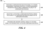
- FIG. 4 is a flow diagram of an example method 400 corresponding to a power configuration component including selectable configuration profiles, in accordance with some embodiments of the present disclosure.
- the method 400 can be performed by processing logic that can include hardware (e.g., processing device, circuitry, dedicated logic, programmable logic, microcode, hardware of a device, integrated circuit, etc.), software (e.g., instructions run or executed on a processing device), or a combination thereof.
- the method 400 is performed by the memory power management component 113 of FIG. 1 . Although shown in a particular sequence or order, unless otherwise specified, the order of the processes can be modified.
- the method 400 can include receiving a configuration selection signal to a power management configuration pin of a power management integrated circuit (PMIC) comprising a plurality of configuration profiles.
- PMIC power management integrated circuit
- the PMIC can have configuration profiles stored thereon. As described above, the configuration profiles correspond to respective sets of operating characteristics of the PMIC.
- the configuration profiles can be stored in a non-volatile memory (NVM) of the PMIC.
- NVM non-volatile memory
- the NVM can be analogous to NVM 214 illustrated in FIG. 2 and/or NVM 314 illustrated in FIG. 3 , herein.
- the NVM can be a OTP memory device in some embodiments.
- the PMIC can be analogous to the power management component 113 illustrated in FIG. 1 , herein.
- the method 400 can include selectively activate a configuration profile among the plurality of configuration profiles based on the configuration signal.
- a configuration selection signal can be received to one or more power management configuration pins of the PMIC to selectively activate one of the configuration profiles.
- the configuration pin can be analogous to configuration pins 208A to 208N illustrated in FIG. 2 , herein.
- receipt of the selection signal at the power management pin of the PMIC can further include receiving the selection signal at a particular bootstrap configuration pin among a set of bootstrap configuration pins of the PMIC.
- a bootstrap configuration pin can be a pin that is activated as part of a bootstrap operation, as described above.
- selective activation of the configuration profile can further include outputting a voltage signal with a magnitude corresponding to the particular set of operating characteristics from the PMIC.
- the method 400 can include providing one or more control signals to the PMIC based on the selectively activated configuration profile.
- the one or more control signals can cause the PMIC to operate according to the particular set of operating characteristics to which the activated one of the configuration profiles corresponds.
- the processing device can determine that the PMIC is to operate according to a particular set of operating characteristics.
- the PMIC can then operate according to a particular set of operating characteristics corresponding to a memory sub-system in which the PMIC will be deployed.
- Embodiments are not so limited, however, and the particular set of operating characteristics under which the PMIC will operate in practice can be determined prior to the PMIC being shipped or sold to an end user.
- selectively activating the configuration profile to cause the PMIC to operate according to the particular set of operating characteristics can further include causing the PMIC to manage a power consumption (e.g., an amount of power provided to a memory sub-system) of a memory sub-system (e.g., memory sub-system 110 illustrated in FIG. 1 , herein) and/or host system (e.g., host system 120 illustrated in FIG. 1 , herein).
- a power consumption e.g., an amount of power provided to a memory sub-system
- host system e.g., host system 120 illustrated in FIG. 1 , herein.
- Selectively activating the configuration profile to cause the PMIC to operate according to the particular set of operating characteristics can further include accessing the NVM (e.g., a OTP memory component of the PMIC) to locate the configuration profile, as discussed in connection with FIG. 3 , herein.
- selective activation of the configuration profile can cause the PMIC to locate the configuration profile using a lookup table stored in a memory location (or memory location partition) of the NVM.
- the configuration profile can be selected by accessing a partition of the NVM (e.g., NVM 314 shown in FIG. 3 ) that stores the desired configuration profile.
- FIG. 5 illustrates an example machine of a computer system 500 within which a set of instructions, for causing the machine to perform any one or more of the methodologies discussed herein, can be executed.
- the computer system 500 can correspond to a host system (e.g., the host system 120 of FIG. 1 ) that includes, is coupled to, or utilizes a memory sub-system (e.g., the memory sub-system 110 of FIG. 1 ) or can be used to perform the operations of a controller (e.g., to execute an operating system to perform operations corresponding to the power management component 113 of FIG. 1 ).
- a host system e.g., the host system 120 of FIG. 1
- a memory sub-system e.g., the memory sub-system 110 of FIG. 1
- a controller e.g., to execute an operating system to perform operations corresponding to the power management component 113 of FIG. 1 .
- the machine can be connected (e.g., networked) to other machines in a LAN, an intranet, an extranet, and/or the Internet.
- the machine can operate in the capacity of a server or a client machine in client-server network environment, as a peer machine in a peer-to-peer (or distributed) network environment, or as a server or a client machine in a cloud computing infrastructure or environment.
- the machine can be a personal computer (PC), a tablet PC, a set-top box (STB), a Personal Digital Assistant (PDA), a cellular telephone, a web appliance, a server, a network router, a switch or bridge, or any machine capable of executing a set of instructions (sequential or otherwise) that specify actions to be taken by that machine.
- PC personal computer
- PDA Personal Digital Assistant
- STB set-top box
- STB set-top box
- a Personal Digital Assistant PDA
- a cellular telephone a web appliance
- server a server
- network router a network router
- switch or bridge any machine capable of executing a set of instructions (sequential or otherwise) that specify actions to be taken by that machine.
- machine shall also be taken to include any collection of machines that individually or jointly execute a set (or multiple sets) of instructions to perform any one or more of the methodologies discussed herein.
- the example computer system 500 includes a processing device 502, a main memory 504 (e.g., read-only memory (ROM), flash memory, dynamic random access memory (DRAM) such as synchronous DRAM (SDRAM) or Rambus DRAM (RDRAM), etc.), a static memory 506 (e.g., flash memory, static random access memory (SRAM), etc.), and a data storage system 518, which communicate with each other via a bus 530.
- main memory 504 e.g., read-only memory (ROM), flash memory, dynamic random access memory (DRAM) such as synchronous DRAM (SDRAM) or Rambus DRAM (RDRAM), etc.
- DRAM dynamic random access memory
- SDRAM synchronous DRAM
- RDRAM Rambus DRAM
- static memory 506 e.g., flash memory, static random access memory (SRAM), etc.
- SRAM static random access memory
- Processing device 502 represents one or more general-purpose processing devices such as a microprocessor, a central processing unit, or the like. More particularly, the processing device can be a complex instruction set computing (CISC) microprocessor, reduced instruction set computing (RISC) microprocessor, very long instruction word (VLIW) microprocessor, or a processor implementing other instruction sets, or processors implementing a combination of instruction sets. Processing device 502 can also be one or more special-purpose processing devices such as an application specific integrated circuit (ASIC), a field programmable gate array (FPGA), a digital signal processor (DSP), network processor, or the like. The processing device 502 is configured to execute instructions 526 for performing the operations and steps discussed herein.
- the computer system 500 can further include a network interface device 508 to communicate over the network 520.
- the data storage system 518 can include a machine-readable storage medium 524 (also known as a computer-readable medium) on which is stored one or more sets of instructions 526 or software embodying any one or more of the methodologies or functions described herein.
- the instructions 526 can also reside, completely or at least partially, within the main memory 504 and/or within the processing device 502 during execution thereof by the computer system 500, the main memory 504 and the processing device 502 also constituting machine-readable storage media.
- the machine-readable storage medium 524, data storage system 518, and/or main memory 604 can correspond to the memory sub-system 110 of FIG. 1 .
- the instructions 526 include instructions to implement functionality corresponding to a power management component (e.g., the power management component 113 of FIG. 1 ).
- a power management component e.g., the power management component 113 of FIG. 1
- the machine-readable storage medium 524 is shown in an example embodiment to be a single medium, the term “machine-readable storage medium” should be taken to include a single medium or multiple media that store the one or more sets of instructions.
- the term “machine-readable storage medium” shall also be taken to include any medium that is capable of storing or encoding a set of instructions for execution by the machine and that cause the machine to perform any one or more of the methodologies of the present disclosure.
- the term “machine-readable storage medium” shall accordingly be taken to include, but not be limited to, solid-state memories, optical media, and magnetic media.
- the present disclosure also relates to an apparatus for performing the operations herein.
- This apparatus can be specially constructed for the intended purposes, or it can include a general purpose computer selectively activated or reconfigured by a computer program stored in the computer.
- a computer program can be stored in a computer readable storage medium, such as, but not limited to, any type of disk including floppy disks, optical disks, CD-ROMs, and magnetic-optical disks, read-only memories (ROMs), random access memories (RAMs), EPROMs, EEPROMs, magnetic or optical cards, or any type of media suitable for storing electronic instructions, each coupled to a computer system bus.
- the present disclosure can be provided as a computer program product, or software, that can include a machine-readable medium having stored thereon instructions, which can be used to program a computer system (or other electronic devices) to perform a process according to the present disclosure.
- a machine-readable medium includes any mechanism for storing information in a form readable by a machine (e.g., a computer).
- a machine-readable (e.g., computer-readable) medium includes a machine (e.g., a computer) readable storage medium such as a read only memory (“ROM”), random access memory (“RAM”), magnetic disk storage media, optical storage media, flash memory components, etc.
Landscapes
- Engineering & Computer Science (AREA)
- Theoretical Computer Science (AREA)
- Physics & Mathematics (AREA)
- General Engineering & Computer Science (AREA)
- General Physics & Mathematics (AREA)
- Software Systems (AREA)
- Human Computer Interaction (AREA)
- Power Engineering (AREA)
- Power Sources (AREA)
- Techniques For Improving Reliability Of Storages (AREA)
Claims (15)
- Vorrichtung, umfassend:einen integrierten Schaltkreis zur Energieverwaltung, PMIC (113, 213), der einen internen Speicher (214) umfasst und dafür eingerichtet ist, an einem Speicher-Subsystem (110) angeordnet zu werden, wobei der interne Speicher (214) dafür konfiguriert ist, eine Vielzahl von Konfigurationsprofilen (131) zu speichern; undKonfigurationskontaktstifte (208A, 208B, 208N), die betrieblich mit dem PMIC (113, 213) gekoppelt sind, wobei einer oder mehrere der Konfigurationskontaktstifte (208A, 208B, 208N) ein Signal empfangen, um mindestens eines aus der Vielzahl von Konfigurationsprofilen (131) zu aktivieren, und wobei das aktivierte mindestens eine aus der Vielzahl von Konfigurationsprofilen (131) bewirkt, dass der PMIC (113, 213) gemäß einer bestimmten Menge von Betriebscharakteristiken arbeitet.
- Vorrichtung nach Anspruch 1, wobei der interne Speicher (214) eine Vielzahl von Speicherstellen (331A, 331B, 331C, 331N) umfasst und wobei jeweilige Konfigurationsprofile (131) aus der Vielzahl von Konfigurationsprofilen (131) in jeweiligen Speicherstellen (331A, 331B, 331C, 331N) des internen Speichers (214) gespeichert sind.
- Vorrichtung nach Anspruch 1, wobei das aktivierte mindestens eine aus der Vielzahl von Konfigurationsprofilen (131) einem Konfigurationsprofil für Peripheral Component Interconnect Express (Peripheriebausteinkopplung-Express, PCIe), einem Konfigurationsprofil für Serial AT Attachment (Serielle AT-Anbindung, SATA), einem Stromausfall-Überbrückungssignal oder einem Stromverbrauchsmodus oder jeglicher Kombination daraus entspricht.
- Vorrichtung nach einem der Ansprüche 1 bis 3, wobei das aktivierte mindestens eine aus der Vielzahl von Konfigurationsprofilen (131) einer jeweils Betriebsspannung, Betriebscharakteristik, Zeitsteuerungscharakteristik oder Kombinationen daraus entspricht als ein anderes der Konfigurationsprofile (131).
- Vorrichtung nach einem der Ansprüche 1 bis 3, wobei der PMIC (113, 213) dafür konfiguriert ist, die Signale von einem Controller (115) zu empfangen, der mit dem Speicher-Subsystem (110) assoziiert ist.
- Vorrichtung nach einem der Ansprüche 1 bis 3, wobei der eine oder die mehreren der Konfigurationskontaktstifte (208A, 208B, 208N) das Signal, um das mindestens eine aus der Vielzahl von Konfigurationsprofilen (131) zu aktivieren, als Antwort auf eine Einschaltoperation empfängt.
- Vorrichtung nach einem der Ansprüche 1 bis 3, wobei der eine oder die mehreren der Konfigurationskontaktstifte (208A, 208B, 208N) das Signal, um das mindestens eine aus der Vielzahl von Konfigurationsprofilen (131) zu aktivieren, als Antwort auf eine Rücksetzoperation empfängt.
- Verfahren, umfassend:Empfangen eines Konfigurationssignals an einem Energieverwaltung-Konfigurationskontaktstift (208A, 208B, 208N) eines integrierten Schaltkreises zur Energieverwaltung, PMIC (113, 213), der einen internen Speicher (214) umfasst, der eine Vielzahl von Konfigurationsprofilen (131) speichert;Aktivieren eines Konfigurationsprofils (131) aus der Vielzahl von Konfigurationsprofilen (131) auf der Grundlage des Konfigurationssignals, um zu bewirken, dass der PMIC (113, 213) selektiv gemäß einer bestimmten Menge von Betriebscharakteristiken arbeitet.
- Verfahren nach Anspruch 8, wobei das Empfangen des Konfigurationssignals ferner das Empfangen des Konfigurationssignals durch einen Bootstrap-Konfigurationskontaktstift des PMIC (113, 213) umfasst.
- Verfahren nach einem der Ansprüche 8 bis 9, wobei das Empfangen des Konfigurationssignals am Energieverwaltung-Konfigurationskontaktstift (208A, 208B, 208N), um das Konfigurationsprofil (131) zu aktivieren, ferner das Empfangen eines Steuerungssignals, das der bestimmten Menge von Betriebscharakteristiken entspricht, vom PMIC (113, 213) umfasst.
- Verfahren nach einem der Ansprüche 8 bis 9, wobei der interne Speicher (214) ein nichtflüchtiger Festwertspeicher ist, in dem die Konfigurationsprofile (131) gespeichert sind.
- Verfahren nach einem der Ansprüche 8 bis 9, wobei das Bewirken, dass der PMIC (113, 213) gemäß der bestimmten Menge von Betriebscharakteristiken arbeitet, ferner das Verwalten eines Stromverbrauchs eines Speicher-Subsystems (110) umfasst.
- Verfahren nach einem der Ansprüche 8 bis 9, wobei das Empfangen des Konfigurationssignals am Energieverwaltung-Konfigurationskontaktstift (208A, 208B, 208N), um das Konfigurationsprofil (131) zu aktivieren, ferner das Zugreifen auf eine im internen Speicher (214) des PMIC (113, 213) gespeicherte Verweistabelle umfasst, um das Konfigurationsprofil (131) zu lokalisieren.
- Verfahren nach einem der Ansprüche 8 bis 9, ferner umfassend das Empfangen des Konfigurationssignals am Energieverwaltung-Konfigurationskontaktstift (208A, 208B, 208N) als Antwort auf eine Einschaltoperation.
- Verfahren nach einem der Ansprüche 8 bis 9, ferner umfassend das Empfangen des Konfigurationssignals am Energieverwaltung-Konfigurationskontaktstift (208A, 208B, 208N) als Antwort auf eine Rücksetzoperation.
Priority Applications (1)
| Application Number | Priority Date | Filing Date | Title |
|---|---|---|---|
| EP25161916.9A EP4542550A3 (de) | 2018-08-09 | 2019-08-01 | Leistungskonfigurationskomponente mit wählbaren konfigurationsprofilen |
Applications Claiming Priority (2)
| Application Number | Priority Date | Filing Date | Title |
|---|---|---|---|
| US16/059,387 US10761588B2 (en) | 2018-08-09 | 2018-08-09 | Power configuration component including selectable configuration profiles corresponding to operating characteristics of the power configuration component |
| PCT/US2019/044672 WO2020033233A1 (en) | 2018-08-09 | 2019-08-01 | Power configuration component including selectable configuration profiles |
Related Child Applications (2)
| Application Number | Title | Priority Date | Filing Date |
|---|---|---|---|
| EP25161916.9A Division EP4542550A3 (de) | 2018-08-09 | 2019-08-01 | Leistungskonfigurationskomponente mit wählbaren konfigurationsprofilen |
| EP25161916.9A Division-Into EP4542550A3 (de) | 2018-08-09 | 2019-08-01 | Leistungskonfigurationskomponente mit wählbaren konfigurationsprofilen |
Publications (3)
| Publication Number | Publication Date |
|---|---|
| EP3834053A1 EP3834053A1 (de) | 2021-06-16 |
| EP3834053A4 EP3834053A4 (de) | 2022-05-04 |
| EP3834053B1 true EP3834053B1 (de) | 2025-04-09 |
Family
ID=69405843
Family Applications (2)
| Application Number | Title | Priority Date | Filing Date |
|---|---|---|---|
| EP25161916.9A Pending EP4542550A3 (de) | 2018-08-09 | 2019-08-01 | Leistungskonfigurationskomponente mit wählbaren konfigurationsprofilen |
| EP19847882.8A Active EP3834053B1 (de) | 2018-08-09 | 2019-08-01 | Leistungskonfigurationskomponente mit auswählbaren konfigurationsprofilen |
Family Applications Before (1)
| Application Number | Title | Priority Date | Filing Date |
|---|---|---|---|
| EP25161916.9A Pending EP4542550A3 (de) | 2018-08-09 | 2019-08-01 | Leistungskonfigurationskomponente mit wählbaren konfigurationsprofilen |
Country Status (5)
| Country | Link |
|---|---|
| US (2) | US10761588B2 (de) |
| EP (2) | EP4542550A3 (de) |
| KR (2) | KR102625101B1 (de) |
| CN (1) | CN112567315B (de) |
| WO (1) | WO2020033233A1 (de) |
Families Citing this family (6)
| Publication number | Priority date | Publication date | Assignee | Title |
|---|---|---|---|---|
| CN111949108B (zh) * | 2020-08-31 | 2022-07-15 | 哲库科技(北京)有限公司 | 一种电源管理装置、方法和设备 |
| US11763040B2 (en) * | 2021-04-07 | 2023-09-19 | Western Digital Technologies, Inc. | Enhanced D3-cold and faster recovery |
| US11538545B2 (en) * | 2021-04-22 | 2022-12-27 | Micron Technology, Inc. | Auto-power on mode for biased testing of a power management integrated circuit (PMIC) |
| KR20230010106A (ko) * | 2021-07-08 | 2023-01-18 | 삼성전자주식회사 | 공유 전압을 공유하는 제1 및 제2 장치들, 및 공유 전압을 생성하도록 구성된 전원 관리 집적 회로를 포함하는 사용자 시스템, 및 그것의 동작 방법 |
| CN115543875B (zh) * | 2022-09-27 | 2024-07-30 | 深圳市紫光同创电子有限公司 | 一次性可编程存储器控制系统和fpga |
| US20240412770A1 (en) * | 2023-06-09 | 2024-12-12 | Micron Technology, Inc. | Sequenced activation of memory components |
Family Cites Families (18)
| Publication number | Priority date | Publication date | Assignee | Title |
|---|---|---|---|---|
| US5825697A (en) * | 1995-12-22 | 1998-10-20 | Micron Technology, Inc. | Circuit and method for enabling a function in a multiple memory device module |
| US6154857A (en) * | 1997-04-08 | 2000-11-28 | Advanced Micro Devices, Inc. | Microprocessor-based device incorporating a cache for capturing software performance profiling data |
| US7010438B2 (en) | 2002-12-23 | 2006-03-07 | Power Measurement Ltd. | Integrated circuit with power monitoring/control and device incorporating same |
| US7904639B2 (en) * | 2006-08-22 | 2011-03-08 | Mosaid Technologies Incorporated | Modular command structure for memory and memory system |
| US7814351B2 (en) | 2007-06-28 | 2010-10-12 | Seagate Technology Llc | Power management in a storage array |
| US8131991B2 (en) * | 2009-02-10 | 2012-03-06 | Sony Corporation | System and method for configuring plural software profiles |
| KR101498225B1 (ko) | 2009-02-19 | 2015-03-04 | 삼성전자주식회사 | 데이터 저장 장치 및 그것의 전원 관리 방법 |
| US20100318824A1 (en) * | 2009-06-10 | 2010-12-16 | Seagate Technology Llc | Storage device with advanced power management |
| GB2472051B (en) * | 2009-07-22 | 2012-10-10 | Wolfson Microelectronics Plc | Power management apparatus and methods |
| US9317212B2 (en) | 2012-12-18 | 2016-04-19 | Intel Corporation | Method and apparatus for controlling a storage device |
| US9195293B1 (en) | 2013-05-03 | 2015-11-24 | Western Digital Technologies, Inc. | User controlled data storage device power and performance settings |
| US9536094B2 (en) | 2014-01-13 | 2017-01-03 | Raytheon Company | Mediated secure boot for single or multicore processors |
| WO2016111670A1 (en) | 2015-01-05 | 2016-07-14 | Hewlett Packard Enterprise Development Lp | Storage device flashing operation |
| KR101824182B1 (ko) | 2016-02-22 | 2018-01-31 | 세종대학교산학협력단 | 전력 관리 기능을 갖는 프로세서 및 프로세서의 전력 관리 방법 |
| JP6808507B2 (ja) | 2017-01-25 | 2021-01-06 | キヤノン株式会社 | 情報処理装置及びその制御方法、並びにプログラム |
| US9984762B1 (en) | 2017-02-16 | 2018-05-29 | Seagate Technology Llc | Cascaded E-fuse switch circuits to control data backup in a storage device |
| US10839862B2 (en) * | 2018-04-25 | 2020-11-17 | Micron Technology, Inc. | Cross point array memory in a non-volatile dual in-line memory module |
| US10877835B2 (en) * | 2018-07-19 | 2020-12-29 | Micron Technology, Inc. | Write buffer management |
-
2018
- 2018-08-09 US US16/059,387 patent/US10761588B2/en active Active
-
2019
- 2019-08-01 EP EP25161916.9A patent/EP4542550A3/de active Pending
- 2019-08-01 KR KR1020237038778A patent/KR102625101B1/ko active Active
- 2019-08-01 CN CN201980052452.5A patent/CN112567315B/zh active Active
- 2019-08-01 EP EP19847882.8A patent/EP3834053B1/de active Active
- 2019-08-01 WO PCT/US2019/044672 patent/WO2020033233A1/en not_active Ceased
- 2019-08-01 KR KR1020217006308A patent/KR102602541B1/ko active Active
-
2020
- 2020-08-18 US US16/996,256 patent/US11269397B2/en active Active
Also Published As
| Publication number | Publication date |
|---|---|
| US20200401202A1 (en) | 2020-12-24 |
| CN112567315B (zh) | 2024-04-30 |
| US11269397B2 (en) | 2022-03-08 |
| KR102625101B1 (ko) | 2024-01-16 |
| EP4542550A2 (de) | 2025-04-23 |
| US20200050252A1 (en) | 2020-02-13 |
| EP3834053A1 (de) | 2021-06-16 |
| EP4542550A3 (de) | 2025-07-09 |
| KR102602541B1 (ko) | 2023-11-15 |
| KR20230160948A (ko) | 2023-11-24 |
| WO2020033233A1 (en) | 2020-02-13 |
| US10761588B2 (en) | 2020-09-01 |
| KR20210031518A (ko) | 2021-03-19 |
| EP3834053A4 (de) | 2022-05-04 |
| CN112567315A (zh) | 2021-03-26 |
Similar Documents
| Publication | Publication Date | Title |
|---|---|---|
| EP3834053B1 (de) | Leistungskonfigurationskomponente mit auswählbaren konfigurationsprofilen | |
| US11347429B2 (en) | Live firmware activation in a memory system | |
| US11809721B2 (en) | Memory sub-system temperature regulation by modifying a data parameter | |
| US20210389910A1 (en) | Managing a memory system including memory devices with different characteristics | |
| US11379032B2 (en) | Power management integrated circuit with in situ non-volatile programmability | |
| US10762968B2 (en) | Dynamic user-selectable trim profile in a memory component | |
| US12578887B2 (en) | Boot process to improve data retention in memory devices | |
| US11221912B2 (en) | Mitigating an undetectable error when retrieving critical data during error handling | |
| CN111886650B (zh) | 以基于温度的频率对存储器系统的存储器单元执行操作 | |
| US11755250B2 (en) | Write type indication command | |
| US20210064278A1 (en) | Managing attributes of memory components | |
| US20250298625A1 (en) | Fast boot of a host system connected to a peripheral device | |
| US12242741B2 (en) | Memory sub-system signature generation | |
| US20260072699A1 (en) | Reducing boot response time in a memory sub-system using a quick boot cpu core | |
| US20250370924A1 (en) | Memory system characteristic control | |
| CN120104153A (zh) | 用于更新诊断能力的固件管理 |
Legal Events
| Date | Code | Title | Description |
|---|---|---|---|
| STAA | Information on the status of an ep patent application or granted ep patent |
Free format text: STATUS: THE INTERNATIONAL PUBLICATION HAS BEEN MADE |
|
| PUAI | Public reference made under article 153(3) epc to a published international application that has entered the european phase |
Free format text: ORIGINAL CODE: 0009012 |
|
| STAA | Information on the status of an ep patent application or granted ep patent |
Free format text: STATUS: REQUEST FOR EXAMINATION WAS MADE |
|
| 17P | Request for examination filed |
Effective date: 20210309 |
|
| AK | Designated contracting states |
Kind code of ref document: A1 Designated state(s): AL AT BE BG CH CY CZ DE DK EE ES FI FR GB GR HR HU IE IS IT LI LT LU LV MC MK MT NL NO PL PT RO RS SE SI SK SM TR |
|
| DAV | Request for validation of the european patent (deleted) | ||
| DAX | Request for extension of the european patent (deleted) | ||
| REG | Reference to a national code |
Ref country code: DE Free format text: PREVIOUS MAIN CLASS: G06F0001320000 Ref country code: DE Ref legal event code: R079 Ref document number: 602019068521 Country of ref document: DE Free format text: PREVIOUS MAIN CLASS: G06F0001320000 Ipc: G06F0001323400 |
|
| A4 | Supplementary search report drawn up and despatched |
Effective date: 20220404 |
|
| RIC1 | Information provided on ipc code assigned before grant |
Ipc: G11C 16/30 20060101ALI20220328BHEP Ipc: G11C 7/10 20060101ALI20220328BHEP Ipc: G11C 5/14 20060101ALI20220328BHEP Ipc: G06F 3/06 20060101ALI20220328BHEP Ipc: G06F 1/3234 20190101AFI20220328BHEP |
|
| GRAP | Despatch of communication of intention to grant a patent |
Free format text: ORIGINAL CODE: EPIDOSNIGR1 |
|
| STAA | Information on the status of an ep patent application or granted ep patent |
Free format text: STATUS: GRANT OF PATENT IS INTENDED |
|
| INTG | Intention to grant announced |
Effective date: 20241028 |
|
| RAP3 | Party data changed (applicant data changed or rights of an application transferred) |
Owner name: MICRON TECHNOLOGY, INC. |
|
| P01 | Opt-out of the competence of the unified patent court (upc) registered |
Free format text: CASE NUMBER: APP_64689/2024 Effective date: 20241206 |
|
| GRAS | Grant fee paid |
Free format text: ORIGINAL CODE: EPIDOSNIGR3 |
|
| GRAA | (expected) grant |
Free format text: ORIGINAL CODE: 0009210 |
|
| STAA | Information on the status of an ep patent application or granted ep patent |
Free format text: STATUS: THE PATENT HAS BEEN GRANTED |
|
| AK | Designated contracting states |
Kind code of ref document: B1 Designated state(s): AL AT BE BG CH CY CZ DE DK EE ES FI FR GB GR HR HU IE IS IT LI LT LU LV MC MK MT NL NO PL PT RO RS SE SI SK SM TR |
|
| REG | Reference to a national code |
Ref country code: GB Ref legal event code: FG4D |
|
| REG | Reference to a national code |
Ref country code: CH Ref legal event code: EP |
|
| REG | Reference to a national code |
Ref country code: DE Ref legal event code: R096 Ref document number: 602019068521 Country of ref document: DE |
|
| REG | Reference to a national code |
Ref country code: IE Ref legal event code: FG4D |
|
| REG | Reference to a national code |
Ref country code: NL Ref legal event code: MP Effective date: 20250409 |
|
| PG25 | Lapsed in a contracting state [announced via postgrant information from national office to epo] |
Ref country code: NL Free format text: LAPSE BECAUSE OF FAILURE TO SUBMIT A TRANSLATION OF THE DESCRIPTION OR TO PAY THE FEE WITHIN THE PRESCRIBED TIME-LIMIT Effective date: 20250409 |
|
| REG | Reference to a national code |
Ref country code: AT Ref legal event code: MK05 Ref document number: 1784113 Country of ref document: AT Kind code of ref document: T Effective date: 20250409 |
|
| PG25 | Lapsed in a contracting state [announced via postgrant information from national office to epo] |
Ref country code: FI Free format text: LAPSE BECAUSE OF FAILURE TO SUBMIT A TRANSLATION OF THE DESCRIPTION OR TO PAY THE FEE WITHIN THE PRESCRIBED TIME-LIMIT Effective date: 20250409 Ref country code: ES Free format text: LAPSE BECAUSE OF FAILURE TO SUBMIT A TRANSLATION OF THE DESCRIPTION OR TO PAY THE FEE WITHIN THE PRESCRIBED TIME-LIMIT Effective date: 20250409 Ref country code: PT Free format text: LAPSE BECAUSE OF FAILURE TO SUBMIT A TRANSLATION OF THE DESCRIPTION OR TO PAY THE FEE WITHIN THE PRESCRIBED TIME-LIMIT Effective date: 20250811 |
|
| PGFP | Annual fee paid to national office [announced via postgrant information from national office to epo] |
Ref country code: DE Payment date: 20250827 Year of fee payment: 7 |
|
| REG | Reference to a national code |
Ref country code: LT Ref legal event code: MG9D |
|
| PG25 | Lapsed in a contracting state [announced via postgrant information from national office to epo] |
Ref country code: NO Free format text: LAPSE BECAUSE OF FAILURE TO SUBMIT A TRANSLATION OF THE DESCRIPTION OR TO PAY THE FEE WITHIN THE PRESCRIBED TIME-LIMIT Effective date: 20250709 Ref country code: GR Free format text: LAPSE BECAUSE OF FAILURE TO SUBMIT A TRANSLATION OF THE DESCRIPTION OR TO PAY THE FEE WITHIN THE PRESCRIBED TIME-LIMIT Effective date: 20250710 |
|
| PG25 | Lapsed in a contracting state [announced via postgrant information from national office to epo] |
Ref country code: PL Free format text: LAPSE BECAUSE OF FAILURE TO SUBMIT A TRANSLATION OF THE DESCRIPTION OR TO PAY THE FEE WITHIN THE PRESCRIBED TIME-LIMIT Effective date: 20250409 |
|
| PG25 | Lapsed in a contracting state [announced via postgrant information from national office to epo] |
Ref country code: BG Free format text: LAPSE BECAUSE OF FAILURE TO SUBMIT A TRANSLATION OF THE DESCRIPTION OR TO PAY THE FEE WITHIN THE PRESCRIBED TIME-LIMIT Effective date: 20250409 |
|
| PGFP | Annual fee paid to national office [announced via postgrant information from national office to epo] |
Ref country code: GB Payment date: 20250826 Year of fee payment: 7 |
|
| PG25 | Lapsed in a contracting state [announced via postgrant information from national office to epo] |
Ref country code: HR Free format text: LAPSE BECAUSE OF FAILURE TO SUBMIT A TRANSLATION OF THE DESCRIPTION OR TO PAY THE FEE WITHIN THE PRESCRIBED TIME-LIMIT Effective date: 20250409 |
|
| PG25 | Lapsed in a contracting state [announced via postgrant information from national office to epo] |
Ref country code: AT Free format text: LAPSE BECAUSE OF FAILURE TO SUBMIT A TRANSLATION OF THE DESCRIPTION OR TO PAY THE FEE WITHIN THE PRESCRIBED TIME-LIMIT Effective date: 20250409 |
|
| PGFP | Annual fee paid to national office [announced via postgrant information from national office to epo] |
Ref country code: FR Payment date: 20250825 Year of fee payment: 7 |
|
| PG25 | Lapsed in a contracting state [announced via postgrant information from national office to epo] |
Ref country code: RS Free format text: LAPSE BECAUSE OF FAILURE TO SUBMIT A TRANSLATION OF THE DESCRIPTION OR TO PAY THE FEE WITHIN THE PRESCRIBED TIME-LIMIT Effective date: 20250709 |
|
| PG25 | Lapsed in a contracting state [announced via postgrant information from national office to epo] |
Ref country code: IS Free format text: LAPSE BECAUSE OF FAILURE TO SUBMIT A TRANSLATION OF THE DESCRIPTION OR TO PAY THE FEE WITHIN THE PRESCRIBED TIME-LIMIT Effective date: 20250809 |
|
| PG25 | Lapsed in a contracting state [announced via postgrant information from national office to epo] |
Ref country code: LV Free format text: LAPSE BECAUSE OF FAILURE TO SUBMIT A TRANSLATION OF THE DESCRIPTION OR TO PAY THE FEE WITHIN THE PRESCRIBED TIME-LIMIT Effective date: 20250409 |
|
| REG | Reference to a national code |
Ref country code: DE Ref legal event code: R097 Ref document number: 602019068521 Country of ref document: DE |
|
| PG25 | Lapsed in a contracting state [announced via postgrant information from national office to epo] |
Ref country code: SM Free format text: LAPSE BECAUSE OF FAILURE TO SUBMIT A TRANSLATION OF THE DESCRIPTION OR TO PAY THE FEE WITHIN THE PRESCRIBED TIME-LIMIT Effective date: 20250409 Ref country code: DK Free format text: LAPSE BECAUSE OF FAILURE TO SUBMIT A TRANSLATION OF THE DESCRIPTION OR TO PAY THE FEE WITHIN THE PRESCRIBED TIME-LIMIT Effective date: 20250409 |
|
| PG25 | Lapsed in a contracting state [announced via postgrant information from national office to epo] |
Ref country code: CZ Free format text: LAPSE BECAUSE OF FAILURE TO SUBMIT A TRANSLATION OF THE DESCRIPTION OR TO PAY THE FEE WITHIN THE PRESCRIBED TIME-LIMIT Effective date: 20250409 |
|
| PG25 | Lapsed in a contracting state [announced via postgrant information from national office to epo] |
Ref country code: EE Free format text: LAPSE BECAUSE OF FAILURE TO SUBMIT A TRANSLATION OF THE DESCRIPTION OR TO PAY THE FEE WITHIN THE PRESCRIBED TIME-LIMIT Effective date: 20250409 |
|
| PG25 | Lapsed in a contracting state [announced via postgrant information from national office to epo] |
Ref country code: SK Free format text: LAPSE BECAUSE OF FAILURE TO SUBMIT A TRANSLATION OF THE DESCRIPTION OR TO PAY THE FEE WITHIN THE PRESCRIBED TIME-LIMIT Effective date: 20250409 Ref country code: RO Free format text: LAPSE BECAUSE OF FAILURE TO SUBMIT A TRANSLATION OF THE DESCRIPTION OR TO PAY THE FEE WITHIN THE PRESCRIBED TIME-LIMIT Effective date: 20250409 |
|
| PG25 | Lapsed in a contracting state [announced via postgrant information from national office to epo] |
Ref country code: IT Free format text: LAPSE BECAUSE OF FAILURE TO SUBMIT A TRANSLATION OF THE DESCRIPTION OR TO PAY THE FEE WITHIN THE PRESCRIBED TIME-LIMIT Effective date: 20250409 |
|
| PLBE | No opposition filed within time limit |
Free format text: ORIGINAL CODE: 0009261 |
|
| STAA | Information on the status of an ep patent application or granted ep patent |
Free format text: STATUS: NO OPPOSITION FILED WITHIN TIME LIMIT |
|
| REG | Reference to a national code |
Ref country code: CH Ref legal event code: L10 Free format text: ST27 STATUS EVENT CODE: U-0-0-L10-L00 (AS PROVIDED BY THE NATIONAL OFFICE) Effective date: 20260218 |
|
| 26N | No opposition filed |
Effective date: 20260112 |
|
| REG | Reference to a national code |
Ref country code: CH Ref legal event code: H13 Free format text: ST27 STATUS EVENT CODE: U-0-0-H10-H13 (AS PROVIDED BY THE NATIONAL OFFICE) Effective date: 20260324 |