EP3833171A1 - Cooling system for power modules - Google Patents
Cooling system for power modules Download PDFInfo
- Publication number
- EP3833171A1 EP3833171A1 EP20210895.7A EP20210895A EP3833171A1 EP 3833171 A1 EP3833171 A1 EP 3833171A1 EP 20210895 A EP20210895 A EP 20210895A EP 3833171 A1 EP3833171 A1 EP 3833171A1
- Authority
- EP
- European Patent Office
- Prior art keywords
- power modules
- neighboring
- cooling system
- coolant
- spaces
- Prior art date
- Legal status (The legal status is an assumption and is not a legal conclusion. Google has not performed a legal analysis and makes no representation as to the accuracy of the status listed.)
- Granted
Links
Images



Classifications
-
- H—ELECTRICITY
- H05—ELECTRIC TECHNIQUES NOT OTHERWISE PROVIDED FOR
- H05K—PRINTED CIRCUITS; CASINGS OR CONSTRUCTIONAL DETAILS OF ELECTRIC APPARATUS; MANUFACTURE OF ASSEMBLAGES OF ELECTRICAL COMPONENTS
- H05K7/00—Constructional details common to different types of electric apparatus
- H05K7/20—Modifications to facilitate cooling, ventilating, or heating
- H05K7/2089—Modifications to facilitate cooling, ventilating, or heating for power electronics, e.g. for inverters for controlling motor
- H05K7/20927—Liquid coolant without phase change
-
- H—ELECTRICITY
- H05—ELECTRIC TECHNIQUES NOT OTHERWISE PROVIDED FOR
- H05K—PRINTED CIRCUITS; CASINGS OR CONSTRUCTIONAL DETAILS OF ELECTRIC APPARATUS; MANUFACTURE OF ASSEMBLAGES OF ELECTRICAL COMPONENTS
- H05K1/00—Printed circuits
- H05K1/02—Details
- H05K1/0201—Thermal arrangements, e.g. for cooling, heating or preventing overheating
- H05K1/0203—Cooling of mounted components
- H05K1/0209—External configuration of printed circuit board adapted for heat dissipation, e.g. lay-out of conductors, coatings
-
- H—ELECTRICITY
- H05—ELECTRIC TECHNIQUES NOT OTHERWISE PROVIDED FOR
- H05K—PRINTED CIRCUITS; CASINGS OR CONSTRUCTIONAL DETAILS OF ELECTRIC APPARATUS; MANUFACTURE OF ASSEMBLAGES OF ELECTRICAL COMPONENTS
- H05K7/00—Constructional details common to different types of electric apparatus
- H05K7/20—Modifications to facilitate cooling, ventilating, or heating
- H05K7/20845—Modifications to facilitate cooling, ventilating, or heating for automotive electronic casings
- H05K7/20872—Liquid coolant without phase change
-
- H—ELECTRICITY
- H05—ELECTRIC TECHNIQUES NOT OTHERWISE PROVIDED FOR
- H05K—PRINTED CIRCUITS; CASINGS OR CONSTRUCTIONAL DETAILS OF ELECTRIC APPARATUS; MANUFACTURE OF ASSEMBLAGES OF ELECTRICAL COMPONENTS
- H05K7/00—Constructional details common to different types of electric apparatus
- H05K7/20—Modifications to facilitate cooling, ventilating, or heating
- H05K7/2089—Modifications to facilitate cooling, ventilating, or heating for power electronics, e.g. for inverters for controlling motor
- H05K7/209—Heat transfer by conduction from internal heat source to heat radiating structure
Definitions
- the present disclosure relates to a cooling system, and more particularly to a cooling system for power modules.
- Power modules for high power conversion typically require liquid coolant to have acceptable size and mass for on-board automotive use.
- the power module is bolted to liquid-cooled heat sink, and the thermal interface material is utilized for transferring the heat from the power module to the heat sink.
- the thermal interface material is difficult to apply consistently and has high thermal resistance.
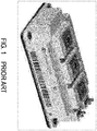
- Even more advanced designs have cooling surfaces on both sides of the power module (see FIG, 2 ), but to date these have only indirect cooling (requiring plural heat sinks and thermal interface material) and are very mechanically complex to assemble and guarantee lifetime performance.
- the structure of the power modules and covers of the cooling system forms the coolant passageway through overmolding, which reduces the external components.
- a cooling system for power modules includes two covers, a plurality of power modules and a plurality of first spaces.
- the plurality of power modules is disposed between the two covers and is arranged in sequence.
- Each of the plurality of power modules includes a housing, a circuit board and a plurality of heat dissipation elements.
- the circuit board is engaged in the housing.
- the plurality of heat dissipation elements is disposed on the two sides of the circuit board.
- Each of the plurality of first spaces is formed between two neighboring power modules of the plurality of power modules or is formed between the cover and the neighboring power module.
- the plurality of heat dissipation elements of each of the plurality of power modules are located in the neighboring first spaces, and the through hole of each of the plurality of power modules is in communication with the neighboring first spaces.
- the plurality of first spaces and the through holes of the plurality of power modules are communicated with each other to form a coolant passageway collaboratively for allowing a coolant to pass through.
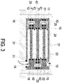
- FIG. 3 is a schematic cross-sectional view of a cooling system for power modules according to an embodiment of the present disclosure.
- the cooling system 1 of the present disclosure includes two covers 11 and 12, a plurality of power modules 21 and a plurality of first spaces 31.
- the plurality of power modules 21 is disposed between the two covers 11 and 12 and is arranged in sequence.
- Each of the plurality of power modules 21 includes a housing 22, a circuit board 23 and a plurality of heat dissipation elements 24.
- the circuit board 23 is engaged in the housing 22.
- the plurality of heat dissipation elements 24 is disposed on the two sides of the circuit board 23.
- the plurality of heat dissipation elements 24 are for example but not limited to molded pin fins, forged pin fins, ribbon bonds, folded fins or lanced fins.
- Each of the plurality of first spaces 31 is formed between two neighboring power modules 21 of the plurality of power modules 21 or is formed between the cover 11 or 12 and the neighboring power module 21.
- the plurality of heat dissipation elements 24 of each of the plurality of power modules 21 are located in the neighboring first spaces 31, and the through hole 25 of each of the plurality of power modules 21 is in communication with the neighboring first spaces 31.
- the two covers are a top cover 11 and a bottom cover 12.
- the top and bottom covers 11 and 12 have a coolant outlet 13 and a coolant inlet 14 respectively.
- the coolant inlet 14 is in communication with the first space 31 formed between the bottom cover 12 and the neighboring power module 21, and the coolant inlet 14 is configured to introduce the coolant into the coolant passageway.
- the coolant outlet 13 is in communication with the first space 31 formed between the top cover 11 and the neighboring power module 21, and the coolant outlet 13 is configured to release the coolant from the coolant passageway.
- the top cover 11 has channels 15 for communicating the coolant outlet 13, the neighboring first space 31 and the through hole 25 of the neighboring power module 21 with each other.
- the bottom cover 12 has channels 16 for communicating the coolant inlet 14, the neighboring first space 31 and the through hole 25 of the neighboring power module 21 with each other. Accordingly, the coolant is introduced into the coolant passageway within the cooling system 1 through the coolant inlet 14, then the coolant flows through the plurality of first spaces 31 along the coolant passageway so as to dissipate the heat generated by the power modules 21, and finally the coolant is released to a space outside the cooling system 1 through the coolant outlet 13.
- the flowing path of the coolant is depicted by arrows.
- the flowing path of coolant shown in figures of the present disclosure can be reversed, and accordingly the coolant inlet 14 and the coolant outlet 13 are exchanged.
- the through holes 25 of the power modules 21, the first spaces 31, the coolant inlet 14 and the coolant outlet 13 can be formed through overmolding.
- the structure of the power modules 21 and covers 11 and 12 of the cooling system 1 forms the coolant passageway through overmolding, which reduces the external components.
- the cooling system 1 further includes plural spacers 41.
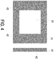
- FIG. 4 schematically shows the top and side views of the spacer of FIG. 3 . Please refer to FIG. 3 and FIG. 4 .
- the first space 31 is located in the middle of the spacer 41.
- Each spacer 41 includes two second spaces 42 in communication with the first space 31 therein, and the two second spaces 42 are in communication with the two through holes 25 of the two neighboring power modules 21 respectively. It is noted that each power module 21 or spacer 41 is flipped over along an axis by 180 degrees relative to the neighboring power module 21 or space 41, and the axis is a normal line to the cross section shown in FIG. 3 .
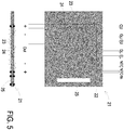
- FIG. 5 schematically shows the top and side views of the power module of FIG. 3 .
- the power module 21 includes power terminals, which are designated as +, - and Out, and the power terminals are symmetrically disposed. Therefore, even if the power module 21 is flipped over along the said axis by 180 degrees, the arrangement of the power terminals is the same.
- the pins of the power module 21, such as CU, GU, EU, GL, EL, NTC and NTC rtn can be varied according to actual requirements.
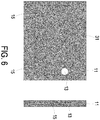
- FIG. 6 schematically shows the top and side views of the top cover of FIG. 3 .
- the coolant outlet 13 is formed on a surface, which is parallel to the power module 21, of the top cover 11. Since the top and bottom covers 11 and 12 are flipped over along the said axis by 180 degrees relative to each other and have the same structure, the coolant inlet 14 is formed on a surface, which is parallel to the power module 21, of the bottom cover 12.
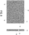
- the location of the coolant inlet 14 and the coolant outlet 13 is not limited thereto. In an embodiment, as shown in FIG. 7 and FIG.
- the coolant outlet 13 may be formed on a surface, which is perpendicular to the power module 21, of the top cover 11 (i.e., the side surface of the top cover 11).
- the coolant inlet 14 may be formed on a surface, which is perpendicular to the power module 21, of the bottom cover 12 (i.e., the side surface of the bottom cover 12).
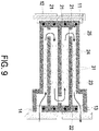
- the spacer 41 in the embodiment of FIG. 3 may be left out, and there is no need to dispose channels in the top and bottom covers 11 and 12.
- the periphery of the housing 22 of the power module 21 is protruded.
- the coolant inlet 14 and coolant outlet 13 are formed on the surfaces perpendicular to the power module 21.
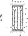
- the coolant inlet 14 and coolant outlet 13 may be formed on the surfaces parallel to the power module 21 in another embodiment, as shown in FIG. 10 .
- the number of the through hole 25 on the housing 22 of the power module 21 is not limited.
- the corresponding cooling system is shown in FIG. 12 and FIG. 13 .
- FIG. 12 and FIG. 13 represent the implementation of the coolant inlet 14 and coolant outlet 13 being formed on the surface perpendicular to the power module 21 and the surface parallel to the power module 21 respectively.
- the centers of the two covers 11 and 12 are both located on a first direction D1.
- the power modules 21 are disposed along the first direction D1 in sequence.
- the arrangement of the power modules 21 is not limited thereto.
- the power modules 21 may be disposed along a second direction D2 in sequence, and the second direction D2 is perpendicular to the first direction D1.
- the cooling system la includes a top cover 11, a bottom cover 12, a first spacer 51, a second spacer 61 and a plurality of power modules 21.
- the first spacer 51 is disposed between the top cover 11 and the plurality of power modules 21.
- the top cover 11 includes a third space 17 in communication with the coolant outlet 13.
- the first spacer 51 has a plurality of openings 52 corresponds to and communicates with the first spaces 31 formed between the top cover 11 and the plurality of power modules 21 respectively, and the plurality of openings 52 of the first spacer 51 is in communication with the third space 17.
- the second spacer 61 is disposed between the bottom cover 12 and the plurality of power modules 21.
- the bottom cover 12 includes a fourth space 18 in communication with the coolant inlet 14.
- the second spacer 61 has a plurality of openings 62 corresponds to and communicates with the first spaces 31 formed between the bottom cover 12 and the plurality of power modules 21 respectively, and the plurality of openings 62 of the second spacer 61 is in communication with the fourth space 18.
- an O-ring 71 is disposed at the junction of two components assembled to each other for prevent the coolant from leaking.
- the O-ring 71 may be disposed at the junction of the two neighboring power modules 21, the junction of the cover 11 or 12 and the neighboring power module 21, and the junction of the spacer 41, 51 or 61 and the neighboring power module 21.
- the present disclosure provides a cooling system for power modules.
- the structure of the power modules and covers of the cooling system forms the coolant passageway through overmolding, which reduces the external components.
Landscapes
- Engineering & Computer Science (AREA)
- Microelectronics & Electronic Packaging (AREA)
- Physics & Mathematics (AREA)
- Thermal Sciences (AREA)
- Cooling Or The Like Of Semiconductors Or Solid State Devices (AREA)
- Cooling Or The Like Of Electrical Apparatus (AREA)
Abstract
Description
- The present disclosure relates to a cooling system, and more particularly to a cooling system for power modules.
- Power modules for high power conversion typically require liquid coolant to have acceptable size and mass for on-board automotive use. As shown in
FIG. 1 , in the first generation designs, the power module is bolted to liquid-cooled heat sink, and the thermal interface material is utilized for transferring the heat from the power module to the heat sink. However, the thermal interface material is difficult to apply consistently and has high thermal resistance. Even more advanced designs have cooling surfaces on both sides of the power module (seeFIG, 2 ), but to date these have only indirect cooling (requiring plural heat sinks and thermal interface material) and are very mechanically complex to assemble and guarantee lifetime performance. - Therefore, there is a need of providing a cooling system for power modules to obviate the drawbacks encountered from the prior arts.
- It is an objective of the present disclosure to provide a cooling system for power modules. The structure of the power modules and covers of the cooling system forms the coolant passageway through overmolding, which reduces the external components.
- In accordance with an aspect of the present disclosure, there is provided a cooling system for power modules. The cooling system includes two covers, a plurality of power modules and a plurality of first spaces. The plurality of power modules is disposed between the two covers and is arranged in sequence. Each of the plurality of power modules includes a housing, a circuit board and a plurality of heat dissipation elements. The circuit board is engaged in the housing. The plurality of heat dissipation elements is disposed on the two sides of the circuit board. There is a through hole on the housing. Each of the plurality of first spaces is formed between two neighboring power modules of the plurality of power modules or is formed between the cover and the neighboring power module. The plurality of heat dissipation elements of each of the plurality of power modules are located in the neighboring first spaces, and the through hole of each of the plurality of power modules is in communication with the neighboring first spaces. The plurality of first spaces and the through holes of the plurality of power modules are communicated with each other to form a coolant passageway collaboratively for allowing a coolant to pass through.
-
-
FIG. 1 is a schematic perspective view of a conventional gel-filled indirect cooling power module; -
FIG. 2 is a schematic cross-sectional view of a conventional double-sided indirect cooling power module; -
FIG. 3 is a schematic cross-sectional view of a cooling system for power modules according to an embodiment of the present disclosure; -
FIG. 4 schematically shows the top and side views of the spacer ofFIG. 3 ; -
FIG. 5 schematically shows the top and side views of the power module ofFIG. 3 ; -
FIG. 6 schematically shows the top and side views of the top cover ofFIG. 3 ; -
FIG. 7 schematically shows a variant of the cooling system for power modules ofFIG. 3 ; -
FIG. 8 schematically shows the top and side views of the top cover ofFIG. 7 ; -
FIG. 9 andFIG. 10 schematically show variants of the cooling system for power modules ofFIG. 3 ; -
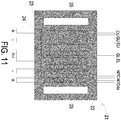
FIG. 11 schematically shows a variant of the power module of the present disclosure; -
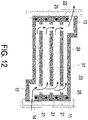
FIG. 12 andFIG. 13 schematically show variants of the cooling systems for power modules ofFIG. 9 andFIG. 10 respectively, wherein the power module ofFIG. 11 is applied in the cooling system; and -
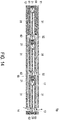
FIG. 14 is a schematic cross-sectional view of a cooling system for power modules according to another embodiment of the present disclosure. - The present disclosure will now be described more specifically with reference to the following embodiments. It is to be noted that the following descriptions of preferred embodiments of this disclosure are presented herein for purpose of illustration and description only. It is not intended to be exhaustive or to be limited to the precise form disclosed.
-
FIG. 3 is a schematic cross-sectional view of a cooling system for power modules according to an embodiment of the present disclosure. As shown inFIG. 3 , the cooling system 1 of the present disclosure includes two covers 11 and 12, a plurality ofpower modules 21 and a plurality offirst spaces 31. The plurality ofpower modules 21 is disposed between the twocovers power modules 21 includes ahousing 22, acircuit board 23 and a plurality ofheat dissipation elements 24. Thecircuit board 23 is engaged in thehousing 22. The plurality ofheat dissipation elements 24 is disposed on the two sides of thecircuit board 23. The plurality ofheat dissipation elements 24 are for example but not limited to molded pin fins, forged pin fins, ribbon bonds, folded fins or lanced fins. There is a throughhole 25 on thehousing 22. Each of the plurality offirst spaces 31 is formed between two neighboringpower modules 21 of the plurality ofpower modules 21 or is formed between thecover power module 21. The plurality ofheat dissipation elements 24 of each of the plurality ofpower modules 21 are located in the neighboringfirst spaces 31, and the throughhole 25 of each of the plurality ofpower modules 21 is in communication with the neighboringfirst spaces 31. - In this embodiment, the two covers are a
top cover 11 and abottom cover 12. The top and bottom covers 11 and 12 have acoolant outlet 13 and acoolant inlet 14 respectively. Thecoolant inlet 14 is in communication with thefirst space 31 formed between thebottom cover 12 and the neighboringpower module 21, and thecoolant inlet 14 is configured to introduce the coolant into the coolant passageway. Thecoolant outlet 13 is in communication with thefirst space 31 formed between thetop cover 11 and the neighboringpower module 21, and thecoolant outlet 13 is configured to release the coolant from the coolant passageway. Thetop cover 11 haschannels 15 for communicating thecoolant outlet 13, the neighboringfirst space 31 and the throughhole 25 of the neighboringpower module 21 with each other. Thebottom cover 12 haschannels 16 for communicating thecoolant inlet 14, the neighboringfirst space 31 and the throughhole 25 of the neighboringpower module 21 with each other. Accordingly, the coolant is introduced into the coolant passageway within the cooling system 1 through thecoolant inlet 14, then the coolant flows through the plurality offirst spaces 31 along the coolant passageway so as to dissipate the heat generated by thepower modules 21, and finally the coolant is released to a space outside the cooling system 1 through thecoolant outlet 13. The flowing path of the coolant is depicted by arrows. Of course, the flowing path of coolant shown in figures of the present disclosure can be reversed, and accordingly thecoolant inlet 14 and thecoolant outlet 13 are exchanged. - In the cooling system 1 of the present disclosure, the through
holes 25 of thepower modules 21, thefirst spaces 31, thecoolant inlet 14 and thecoolant outlet 13 can be formed through overmolding. In other words, the structure of thepower modules 21 and covers 11 and 12 of the cooling system 1 forms the coolant passageway through overmolding, which reduces the external components. - In the embodiment shown in
FIG. 3 , the cooling system 1 further includesplural spacers 41.FIG. 4 schematically shows the top and side views of the spacer ofFIG. 3 . Please refer toFIG. 3 andFIG. 4 . There is onespacer 41 between any two neighboringpower modules 21, and thus the number of thespacers 41 is less than the number of thepower modules 21 by one. Thefirst space 31 is located in the middle of thespacer 41. Eachspacer 41 includes twosecond spaces 42 in communication with thefirst space 31 therein, and the twosecond spaces 42 are in communication with the two throughholes 25 of the two neighboringpower modules 21 respectively. It is noted that eachpower module 21 orspacer 41 is flipped over along an axis by 180 degrees relative to the neighboringpower module 21 orspace 41, and the axis is a normal line to the cross section shown inFIG. 3 . -
FIG. 5 schematically shows the top and side views of the power module ofFIG. 3 . As shown inFIG. 5 , thepower module 21 includes power terminals, which are designated as +, - and Out, and the power terminals are symmetrically disposed. Therefore, even if thepower module 21 is flipped over along the said axis by 180 degrees, the arrangement of the power terminals is the same. In addition, the pins of thepower module 21, such as CU, GU, EU, GL, EL, NTC and NTC rtn, can be varied according to actual requirements. -
FIG. 6 schematically shows the top and side views of the top cover ofFIG. 3 . Please refer toFIG. 3 andFIG. 6 . In this embodiment, thecoolant outlet 13 is formed on a surface, which is parallel to thepower module 21, of thetop cover 11. Since the top and bottom covers 11 and 12 are flipped over along the said axis by 180 degrees relative to each other and have the same structure, thecoolant inlet 14 is formed on a surface, which is parallel to thepower module 21, of thebottom cover 12. However, the location of thecoolant inlet 14 and thecoolant outlet 13 is not limited thereto. In an embodiment, as shown inFIG. 7 andFIG. 8 , thecoolant outlet 13 may be formed on a surface, which is perpendicular to thepower module 21, of the top cover 11 (i.e., the side surface of the top cover 11). Thecoolant inlet 14 may be formed on a surface, which is perpendicular to thepower module 21, of the bottom cover 12 (i.e., the side surface of the bottom cover 12). - In an embodiment, as shown in
FIG. 9 , thespacer 41 in the embodiment ofFIG. 3 may be left out, and there is no need to dispose channels in the top and bottom covers 11 and 12. In order to form thefirst spaces 31 while stacking thepower modules 21, the periphery of thehousing 22 of thepower module 21 is protruded. InFIG. 9 , thecoolant inlet 14 andcoolant outlet 13 are formed on the surfaces perpendicular to thepower module 21. Thecoolant inlet 14 andcoolant outlet 13 may be formed on the surfaces parallel to thepower module 21 in another embodiment, as shown inFIG. 10 . - In addition, the number of the through
hole 25 on thehousing 22 of thepower module 21 is not limited. For example, as shown inFIG. 11 , there may be two throughholes 25 on thehousing 22 of thepower module 21, and the two throughholes 25 are located at the two sides of thecircuit board 23 and are in communication with the neighboringfirst spaces 31. The corresponding cooling system is shown inFIG. 12 andFIG. 13 .FIG. 12 andFIG. 13 represent the implementation of thecoolant inlet 14 andcoolant outlet 13 being formed on the surface perpendicular to thepower module 21 and the surface parallel to thepower module 21 respectively. - In the present application, the centers of the two covers 11 and 12 are both located on a first direction D1. Further, in above embodiments, the
power modules 21 are disposed along the first direction D1 in sequence. However, the arrangement of thepower modules 21 is not limited thereto. In an embodiment, as shown inFIG. 14 , thepower modules 21 may be disposed along a second direction D2 in sequence, and the second direction D2 is perpendicular to the first direction D1. In the embodiment shown inFIG. 14 , the cooling system la includes atop cover 11, abottom cover 12, afirst spacer 51, a second spacer 61 and a plurality ofpower modules 21. Thefirst spacer 51 is disposed between thetop cover 11 and the plurality ofpower modules 21. Thetop cover 11 includes athird space 17 in communication with thecoolant outlet 13. Thefirst spacer 51 has a plurality ofopenings 52 corresponds to and communicates with thefirst spaces 31 formed between thetop cover 11 and the plurality ofpower modules 21 respectively, and the plurality ofopenings 52 of thefirst spacer 51 is in communication with thethird space 17. The second spacer 61 is disposed between thebottom cover 12 and the plurality ofpower modules 21. Thebottom cover 12 includes afourth space 18 in communication with thecoolant inlet 14. The second spacer 61 has a plurality ofopenings 62 corresponds to and communicates with thefirst spaces 31 formed between thebottom cover 12 and the plurality ofpower modules 21 respectively, and the plurality ofopenings 62 of the second spacer 61 is in communication with thefourth space 18. - In an embodiment, as shown in
FIG. 3 , an O-ring 71 is disposed at the junction of two components assembled to each other for prevent the coolant from leaking. For example, the O-ring 71 may be disposed at the junction of the twoneighboring power modules 21, the junction of thecover power module 21, and the junction of thespacer power module 21. - From the above descriptions, the present disclosure provides a cooling system for power modules. The structure of the power modules and covers of the cooling system forms the coolant passageway through overmolding, which reduces the external components.
Claims (12)
- A cooling system (1, 1a) for power modules, characterized by comprising:two covers (11, 12);a plurality of power modules (21) disposed between the two covers (11, 12) and arranged in sequence, wherein each of the plurality of power modules (21) comprises a housing (22), a circuit board (23) and a plurality of heat dissipation elements (24), the circuit board (23) is engaged in the housing (22), the plurality of heat dissipation elements (24) are disposed on the two sides of the circuit board (23), and there is a through hole (25) on the housing (22); anda plurality of first spaces (31), wherein each of the plurality of first spaces (31) is formed between two neighboring power modules of the plurality of power modules (21) or is formed between the cover (11, 12) and the neighboring power module (21), wherein the plurality of heat dissipation elements (24) of each of the plurality of power modules (21) are located in the neighboring first spaces (31), and the through hole (25) of each of the plurality of power modules (21) are in communication with the neighboring first spaces (31),wherein the plurality of first spaces (31) and the through holes (25) of the plurality of power modules (21) are communicated with each other to form a coolant passageway collaboratively for allowing a coolant to pass through.
- The cooling system (1, 1a) according to claim 1, wherein the two covers are a top cover (11) and a bottom cover (12), the top and bottom covers (11, 12) have a coolant outlet (13) and a coolant inlet (14) respectively, the coolant inlet (14) is in communication with the first space (31) formed between the bottom cover (12) and the neighboring power module (21) and is configured to introduce the coolant into the coolant passageway, and the coolant outlet (13) is in communication with the first space (31) formed between the top cover (11) and the neighboring power module (21) and is configured to release the coolant from the coolant passageway.
- The cooling system (1) according to claim 2, wherein centers of the two covers (11, 12) are both located on a first direction (D1), and the plurality of power modules (21) are disposed along the first direction (D1) in sequence.
- The cooling system (1) according to claim 3, wherein there are two through holes (25) on the housing (22) of each of the plurality of power modules (21), and the two through holes (25) are located at two sides of the circuit board (23) and in communication with the neighboring first spaces (31).
- The cooling system (1) according to claim 3, wherein the coolant inlet (14) is formed on a surface parallel to the power module (21) or a surface perpendicular to the power module (21), and the coolant outlet (13) is formed on a surface parallel to the power module (21) or a surface perpendicular to the power module (21).
- The cooling system (1) according to claim 3, wherein there is a spacer (41) between any two neighboring power modules of the plurality of power modules (21), the spacer (41) comprises two second spaces (42) in communication with the corresponding first space (31), and the two second spaces (42) are in communication with the through holes (25) of the two neighboring power modules (21) respectively.
- The cooling system (1) according to claim 3, wherein the top cover (11) has channels (15) for communicating the coolant outlet (13), the neighboring first space (31) and the through hole (25) of the neighboring power module (21) with each other, and the bottom cover (12) has channels (16) for communicating the coolant inlet (14), the neighboring first space (31) and the through hole (25) of the neighboring power module (21) with each other.
- The cooling system (1a) according to claim 2, wherein centers of the two covers (11, 12) are both located on a first direction (D1), and the plurality of power modules (21) are disposed along a second direction (D2) perpendicular to the first direction (D1) in sequence.
- The cooling system (1a) according to claim 8, further comprising a first spacer (51), wherein the first spacer (51) is disposed between the top cover (11) and the plurality of power modules (21), the top cover (11) comprises a third space (17) in communication with the coolant outlet (13), the first spacer (51) has a plurality of openings (52) corresponds to and communicates with the first spaces (31) formed between the top cover (11) and the plurality of power modules (21) respectively, and the plurality of openings (52) of the first spacer (51) is in communication with the third space (17).
- The cooling system (1a) according to claim 8, further comprising a second spacer (61), wherein the second spacer (61) is disposed between the bottom cover (12) and the plurality of power modules (21), the bottom cover (12) comprises a fourth space (18) in communication with the coolant inlet (14), the second spacer (61) has a plurality of openings (62) corresponds to and communicates with the first spaces (31) formed between the bottom cover (12) and the plurality of power modules (21) respectively, and the plurality of openings (62) of the second spacer (61) is in communication with the fourth space (18).
- The cooling system (1, 1a) according to claim 1, wherein each of the plurality of power modules (21) comprises power terminals (+, -, Out) which are symmetrically disposed.
- The cooling system (1, 1a) according to claim 1, wherein the plurality of heat dissipation elements (24) are molded pin fins, forged pin fins, ribbon bonds, folded fins or lanced fins.
Applications Claiming Priority (1)
| Application Number | Priority Date | Filing Date | Title |
|---|---|---|---|
| US201962944697P | 2019-12-06 | 2019-12-06 |
Publications (3)
| Publication Number | Publication Date |
|---|---|
| EP3833171A1 true EP3833171A1 (en) | 2021-06-09 |
| EP3833171B1 EP3833171B1 (en) | 2023-12-27 |
| EP3833171C0 EP3833171C0 (en) | 2023-12-27 |
Family
ID=73654666
Family Applications (1)
| Application Number | Title | Priority Date | Filing Date |
|---|---|---|---|
| EP20210895.7A Active EP3833171B1 (en) | 2019-12-06 | 2020-12-01 | Cooling system for power modules |
Country Status (3)
| Country | Link |
|---|---|
| US (1) | US11324148B2 (en) |
| EP (1) | EP3833171B1 (en) |
| CN (1) | CN112930077B (en) |
Families Citing this family (2)
| Publication number | Priority date | Publication date | Assignee | Title |
|---|---|---|---|---|
| CN118785649A (en) * | 2023-04-06 | 2024-10-15 | 台达电子工业股份有限公司 | Power module heat dissipation assembly structure |
| US20240373598A1 (en) * | 2023-05-05 | 2024-11-07 | Ford Global Technologies, Llc | Electrified vehicle inverter power module cooling |
Citations (5)
| Publication number | Priority date | Publication date | Assignee | Title |
|---|---|---|---|---|
| EP1815514A1 (en) * | 2004-11-24 | 2007-08-08 | Danfoss Silicon Power GmbH | A flow distribution module and a stack of flow distribution modules |
| US20110316143A1 (en) * | 2010-06-23 | 2011-12-29 | Denso Corporation | Semiconductor module with cooling mechanism and production method thereof |
| US20120001341A1 (en) * | 2010-06-30 | 2012-01-05 | Denso Corporation | Semiconductor device |
| CN106783766A (en) * | 2017-03-02 | 2017-05-31 | 中国第汽车股份有限公司 | A kind of IGBT power modules of high integration |
| DE102016223889A1 (en) * | 2016-12-01 | 2018-06-07 | Zf Friedrichshafen Ag | Stackable electronics module, inverter and automotive powertrain |
Family Cites Families (21)
| Publication number | Priority date | Publication date | Assignee | Title |
|---|---|---|---|---|
| US4912600A (en) * | 1988-09-07 | 1990-03-27 | Auburn Univ. Of The State Of Alabama | Integrated circuit packaging and cooling |
| US5121290A (en) * | 1990-06-25 | 1992-06-09 | At&T Bell Laboratories | Circuit pack cooling using perforations |
| DK174881B1 (en) | 2002-05-08 | 2004-01-19 | Danfoss Silicon Power Gmbh | Multiple cooling cell device for cooling semiconductors |
| SG104348A1 (en) * | 2002-11-21 | 2004-06-21 | Inst Of Microelectronics | Apparatus and method for fluid-based cooling of heat-generating devices |
| EP2216891B1 (en) * | 2003-08-21 | 2012-01-04 | Denso Corporation | Mounting structure ofa semiconductor device |
| US7009842B2 (en) * | 2004-01-30 | 2006-03-07 | Isothermal Systems Research, Inc. | Three dimensional packaging and cooling of mixed signal, mixed power density electronic modules |
| KR101029021B1 (en) * | 2005-12-02 | 2011-04-14 | 주식회사 엘지화학 | High Cooling Battery Module |
| US7602608B2 (en) * | 2006-02-06 | 2009-10-13 | Isothermal Systems Research, Inc. | Narrow gap spray cooling in a globally cooled enclosure |
| US20070204646A1 (en) | 2006-03-01 | 2007-09-06 | Thomas Gagliano | Cold plate incorporating a heat pipe |
| US7969734B2 (en) * | 2007-01-03 | 2011-06-28 | General Electric Company | Unique cooling scheme for advanced thermal management of high flux electronics |
| US7965508B2 (en) * | 2007-03-27 | 2011-06-21 | Denso Corporation | Cooling device for electronic component and power converter equipped with the same |
| JP4719187B2 (en) * | 2007-06-15 | 2011-07-06 | トヨタ自動車株式会社 | Semiconductor device cooling structure |
| US20100284149A1 (en) * | 2009-05-05 | 2010-11-11 | Enermax Technology Corporation | Power supply and a housing structure with the power supply |
| JP5627499B2 (en) * | 2010-03-30 | 2014-11-19 | 株式会社デンソー | Semiconductor device provided with semiconductor module |
| US8391008B2 (en) * | 2011-02-17 | 2013-03-05 | Toyota Motor Engineering & Manufacturing North America, Inc. | Power electronics modules and power electronics module assemblies |
| JP5621908B2 (en) * | 2011-03-10 | 2014-11-12 | トヨタ自動車株式会社 | Cooler |
| CN202513237U (en) * | 2012-04-27 | 2012-10-31 | 中国东方电气集团有限公司 | Cooling system and fuel cell stack |
| CN206412334U (en) | 2016-12-01 | 2017-08-15 | 江苏宏微科技股份有限公司 | A kind of two-sided power model for directly cooling down radiator structure |
| US10665525B2 (en) | 2018-05-01 | 2020-05-26 | Semiconductor Components Industries, Llc | Heat transfer for power modules |
| US11467637B2 (en) * | 2018-07-31 | 2022-10-11 | Wuxi Kalannipu Thermal Management Technology Co., Ltd. | Modular computer cooling system |
| CN110112507B (en) | 2019-05-23 | 2021-02-12 | 华霆(合肥)动力技术有限公司 | Thermal management device, power supply system and thermal management method |
-
2020
- 2020-12-01 EP EP20210895.7A patent/EP3833171B1/en active Active
- 2020-12-01 CN CN202011389603.7A patent/CN112930077B/en active Active
- 2020-12-01 US US17/108,123 patent/US11324148B2/en active Active
Patent Citations (5)
| Publication number | Priority date | Publication date | Assignee | Title |
|---|---|---|---|---|
| EP1815514A1 (en) * | 2004-11-24 | 2007-08-08 | Danfoss Silicon Power GmbH | A flow distribution module and a stack of flow distribution modules |
| US20110316143A1 (en) * | 2010-06-23 | 2011-12-29 | Denso Corporation | Semiconductor module with cooling mechanism and production method thereof |
| US20120001341A1 (en) * | 2010-06-30 | 2012-01-05 | Denso Corporation | Semiconductor device |
| DE102016223889A1 (en) * | 2016-12-01 | 2018-06-07 | Zf Friedrichshafen Ag | Stackable electronics module, inverter and automotive powertrain |
| CN106783766A (en) * | 2017-03-02 | 2017-05-31 | 中国第汽车股份有限公司 | A kind of IGBT power modules of high integration |
Also Published As
| Publication number | Publication date |
|---|---|
| EP3833171B1 (en) | 2023-12-27 |
| EP3833171C0 (en) | 2023-12-27 |
| CN112930077B (en) | 2023-11-07 |
| US20210176901A1 (en) | 2021-06-10 |
| US11324148B2 (en) | 2022-05-03 |
| CN112930077A (en) | 2021-06-08 |
Similar Documents
| Publication | Publication Date | Title |
|---|---|---|
| US6466441B1 (en) | Cooling device of electronic part having high and low heat generating elements | |
| US20210243923A1 (en) | Power module assembly | |
| EP3905318A1 (en) | Power module assembly | |
| US8451609B2 (en) | Cooling device for a plurality of power modules | |
| US20160073556A1 (en) | Electric Power Convertor | |
| US20170164516A1 (en) | Integrated Fluid Turbulator and Sealing System for Improved Thermal Management | |
| US11324148B2 (en) | Cooling system for power modules | |
| EP3883353B1 (en) | Automotive electronic device | |
| EP3098845A1 (en) | Package assembly | |
| US6130818A (en) | Electronic assembly with fault tolerant cooling | |
| US20130341782A1 (en) | Semiconductor package module | |
| JP4581802B2 (en) | Thermoelectric converter | |
| CN104617089B (en) | The installation constitution of transmission module | |
| CN218499486U (en) | Work assembly and electronic equipment | |
| KR101360730B1 (en) | Cooling device and electronic device thereof | |
| CN218499488U (en) | Electronic equipment | |
| GB2565071A (en) | Semiconductor module | |
| EP2992577B1 (en) | Cooling device for cooling a laser arrangement and laser system comprising cooling devices | |
| EP4088315B1 (en) | A heatsink with increased air flow | |
| KR20130012650A (en) | Cooling system for junction box | |
| EP3432696B1 (en) | Heat transfer assembly for a heat emitting device | |
| US12593412B2 (en) | Electronic control device | |
| EP3340292B1 (en) | Heat sink, power electronics unit comprising the heat sink and method for assembling the power electronics unit | |
| JP7832396B2 (en) | Liquid cooling device and heat dissipation assembly structure using the same | |
| US12471250B1 (en) | Liquid cooling assembly for electronic components on printed circuit boards and computing device including same |
Legal Events
| Date | Code | Title | Description |
|---|---|---|---|
| PUAI | Public reference made under article 153(3) epc to a published international application that has entered the european phase |
Free format text: ORIGINAL CODE: 0009012 |
|
| STAA | Information on the status of an ep patent application or granted ep patent |
Free format text: STATUS: THE APPLICATION HAS BEEN PUBLISHED |
|
| AK | Designated contracting states |
Kind code of ref document: A1 Designated state(s): AL AT BE BG CH CY CZ DE DK EE ES FI FR GB GR HR HU IE IS IT LI LT LU LV MC MK MT NL NO PL PT RO RS SE SI SK SM TR |
|
| STAA | Information on the status of an ep patent application or granted ep patent |
Free format text: STATUS: REQUEST FOR EXAMINATION WAS MADE |
|
| 17P | Request for examination filed |
Effective date: 20211209 |
|
| RBV | Designated contracting states (corrected) |
Designated state(s): AL AT BE BG CH CY CZ DE DK EE ES FI FR GB GR HR HU IE IS IT LI LT LU LV MC MK MT NL NO PL PT RO RS SE SI SK SM TR |
|
| GRAP | Despatch of communication of intention to grant a patent |
Free format text: ORIGINAL CODE: EPIDOSNIGR1 |
|
| STAA | Information on the status of an ep patent application or granted ep patent |
Free format text: STATUS: GRANT OF PATENT IS INTENDED |
|
| INTG | Intention to grant announced |
Effective date: 20230703 |
|
| GRAS | Grant fee paid |
Free format text: ORIGINAL CODE: EPIDOSNIGR3 |
|
| GRAA | (expected) grant |
Free format text: ORIGINAL CODE: 0009210 |
|
| STAA | Information on the status of an ep patent application or granted ep patent |
Free format text: STATUS: THE PATENT HAS BEEN GRANTED |
|
| AK | Designated contracting states |
Kind code of ref document: B1 Designated state(s): AL AT BE BG CH CY CZ DE DK EE ES FI FR GB GR HR HU IE IS IT LI LT LU LV MC MK MT NL NO PL PT RO RS SE SI SK SM TR |
|
| REG | Reference to a national code |
Ref country code: GB Ref legal event code: FG4D |
|
| REG | Reference to a national code |
Ref country code: CH Ref legal event code: EP |
|
| REG | Reference to a national code |
Ref country code: DE Ref legal event code: R096 Ref document number: 602020023332 Country of ref document: DE |
|
| REG | Reference to a national code |
Ref country code: IE Ref legal event code: FG4D |
|
| U01 | Request for unitary effect filed |
Effective date: 20231227 |
|
| U07 | Unitary effect registered |
Designated state(s): AT BE BG DE DK EE FI FR IT LT LU LV MT NL PT SE SI Effective date: 20240108 |
|
| PG25 | Lapsed in a contracting state [announced via postgrant information from national office to epo] |
Ref country code: GR Free format text: LAPSE BECAUSE OF FAILURE TO SUBMIT A TRANSLATION OF THE DESCRIPTION OR TO PAY THE FEE WITHIN THE PRESCRIBED TIME-LIMIT Effective date: 20240328 |
|
| PG25 | Lapsed in a contracting state [announced via postgrant information from national office to epo] |
Ref country code: ES Free format text: LAPSE BECAUSE OF FAILURE TO SUBMIT A TRANSLATION OF THE DESCRIPTION OR TO PAY THE FEE WITHIN THE PRESCRIBED TIME-LIMIT Effective date: 20231227 |
|
| PG25 | Lapsed in a contracting state [announced via postgrant information from national office to epo] |
Ref country code: GR Free format text: LAPSE BECAUSE OF FAILURE TO SUBMIT A TRANSLATION OF THE DESCRIPTION OR TO PAY THE FEE WITHIN THE PRESCRIBED TIME-LIMIT Effective date: 20240328 Ref country code: ES Free format text: LAPSE BECAUSE OF FAILURE TO SUBMIT A TRANSLATION OF THE DESCRIPTION OR TO PAY THE FEE WITHIN THE PRESCRIBED TIME-LIMIT Effective date: 20231227 |
|
| PG25 | Lapsed in a contracting state [announced via postgrant information from national office to epo] |
Ref country code: RS Free format text: LAPSE BECAUSE OF FAILURE TO SUBMIT A TRANSLATION OF THE DESCRIPTION OR TO PAY THE FEE WITHIN THE PRESCRIBED TIME-LIMIT Effective date: 20231227 Ref country code: NO Free format text: LAPSE BECAUSE OF FAILURE TO SUBMIT A TRANSLATION OF THE DESCRIPTION OR TO PAY THE FEE WITHIN THE PRESCRIBED TIME-LIMIT Effective date: 20240327 Ref country code: HR Free format text: LAPSE BECAUSE OF FAILURE TO SUBMIT A TRANSLATION OF THE DESCRIPTION OR TO PAY THE FEE WITHIN THE PRESCRIBED TIME-LIMIT Effective date: 20231227 |
|
| PG25 | Lapsed in a contracting state [announced via postgrant information from national office to epo] |
Ref country code: IS Free format text: LAPSE BECAUSE OF FAILURE TO SUBMIT A TRANSLATION OF THE DESCRIPTION OR TO PAY THE FEE WITHIN THE PRESCRIBED TIME-LIMIT Effective date: 20240427 |
|
| PG25 | Lapsed in a contracting state [announced via postgrant information from national office to epo] |
Ref country code: CZ Free format text: LAPSE BECAUSE OF FAILURE TO SUBMIT A TRANSLATION OF THE DESCRIPTION OR TO PAY THE FEE WITHIN THE PRESCRIBED TIME-LIMIT Effective date: 20231227 |
|
| PG25 | Lapsed in a contracting state [announced via postgrant information from national office to epo] |
Ref country code: SK Free format text: LAPSE BECAUSE OF FAILURE TO SUBMIT A TRANSLATION OF THE DESCRIPTION OR TO PAY THE FEE WITHIN THE PRESCRIBED TIME-LIMIT Effective date: 20231227 |
|
| PG25 | Lapsed in a contracting state [announced via postgrant information from national office to epo] |
Ref country code: SM Free format text: LAPSE BECAUSE OF FAILURE TO SUBMIT A TRANSLATION OF THE DESCRIPTION OR TO PAY THE FEE WITHIN THE PRESCRIBED TIME-LIMIT Effective date: 20231227 Ref country code: SK Free format text: LAPSE BECAUSE OF FAILURE TO SUBMIT A TRANSLATION OF THE DESCRIPTION OR TO PAY THE FEE WITHIN THE PRESCRIBED TIME-LIMIT Effective date: 20231227 Ref country code: RO Free format text: LAPSE BECAUSE OF FAILURE TO SUBMIT A TRANSLATION OF THE DESCRIPTION OR TO PAY THE FEE WITHIN THE PRESCRIBED TIME-LIMIT Effective date: 20231227 Ref country code: IS Free format text: LAPSE BECAUSE OF FAILURE TO SUBMIT A TRANSLATION OF THE DESCRIPTION OR TO PAY THE FEE WITHIN THE PRESCRIBED TIME-LIMIT Effective date: 20240427 Ref country code: CZ Free format text: LAPSE BECAUSE OF FAILURE TO SUBMIT A TRANSLATION OF THE DESCRIPTION OR TO PAY THE FEE WITHIN THE PRESCRIBED TIME-LIMIT Effective date: 20231227 |
|
| PG25 | Lapsed in a contracting state [announced via postgrant information from national office to epo] |
Ref country code: PL Free format text: LAPSE BECAUSE OF FAILURE TO SUBMIT A TRANSLATION OF THE DESCRIPTION OR TO PAY THE FEE WITHIN THE PRESCRIBED TIME-LIMIT Effective date: 20231227 |
|
| PG25 | Lapsed in a contracting state [announced via postgrant information from national office to epo] |
Ref country code: PL Free format text: LAPSE BECAUSE OF FAILURE TO SUBMIT A TRANSLATION OF THE DESCRIPTION OR TO PAY THE FEE WITHIN THE PRESCRIBED TIME-LIMIT Effective date: 20231227 |
|
| REG | Reference to a national code |
Ref country code: DE Ref legal event code: R097 Ref document number: 602020023332 Country of ref document: DE |
|
| PLBE | No opposition filed within time limit |
Free format text: ORIGINAL CODE: 0009261 |
|
| STAA | Information on the status of an ep patent application or granted ep patent |
Free format text: STATUS: NO OPPOSITION FILED WITHIN TIME LIMIT |
|
| 26N | No opposition filed |
Effective date: 20240930 |
|
| U20 | Renewal fee for the european patent with unitary effect paid |
Year of fee payment: 5 Effective date: 20241107 |
|
| PG25 | Lapsed in a contracting state [announced via postgrant information from national office to epo] |
Ref country code: MC Free format text: LAPSE BECAUSE OF FAILURE TO SUBMIT A TRANSLATION OF THE DESCRIPTION OR TO PAY THE FEE WITHIN THE PRESCRIBED TIME-LIMIT Effective date: 20231227 |
|
| REG | Reference to a national code |
Ref country code: CH Ref legal event code: PL |
|
| GBPC | Gb: european patent ceased through non-payment of renewal fee |
Effective date: 20241201 |
|
| PG25 | Lapsed in a contracting state [announced via postgrant information from national office to epo] |
Ref country code: GB Free format text: LAPSE BECAUSE OF NON-PAYMENT OF DUE FEES Effective date: 20241201 |
|
| PG25 | Lapsed in a contracting state [announced via postgrant information from national office to epo] |
Ref country code: CH Free format text: LAPSE BECAUSE OF NON-PAYMENT OF DUE FEES Effective date: 20241231 |
|
| PG25 | Lapsed in a contracting state [announced via postgrant information from national office to epo] |
Ref country code: IE Free format text: LAPSE BECAUSE OF NON-PAYMENT OF DUE FEES Effective date: 20241201 |
|
| U20 | Renewal fee for the european patent with unitary effect paid |
Year of fee payment: 6 Effective date: 20251110 |
|
| PG25 | Lapsed in a contracting state [announced via postgrant information from national office to epo] |
Ref country code: CY Free format text: LAPSE BECAUSE OF FAILURE TO SUBMIT A TRANSLATION OF THE DESCRIPTION OR TO PAY THE FEE WITHIN THE PRESCRIBED TIME-LIMIT; INVALID AB INITIO Effective date: 20201201 |