EP3832737B1 - Method of manufacturing a hetero-junction solar cell - Google Patents
Method of manufacturing a hetero-junction solar cell Download PDFInfo
- Publication number
- EP3832737B1 EP3832737B1 EP21150107.7A EP21150107A EP3832737B1 EP 3832737 B1 EP3832737 B1 EP 3832737B1 EP 21150107 A EP21150107 A EP 21150107A EP 3832737 B1 EP3832737 B1 EP 3832737B1
- Authority
- EP
- European Patent Office
- Prior art keywords
- layer
- semiconductor substrate
- coating
- edge
- conductive
- Prior art date
- Legal status (The legal status is an assumption and is not a legal conclusion. Google has not performed a legal analysis and makes no representation as to the accuracy of the status listed.)
- Active
Links
Images


Classifications
-
- H—ELECTRICITY
- H10—SEMICONDUCTOR DEVICES; ELECTRIC SOLID-STATE DEVICES NOT OTHERWISE PROVIDED FOR
- H10F—INORGANIC SEMICONDUCTOR DEVICES SENSITIVE TO INFRARED RADIATION, LIGHT, ELECTROMAGNETIC RADIATION OF SHORTER WAVELENGTH OR CORPUSCULAR RADIATION
- H10F77/00—Constructional details of devices covered by this subclass
- H10F77/20—Electrodes
- H10F77/206—Electrodes for devices having potential barriers
- H10F77/211—Electrodes for devices having potential barriers for photovoltaic cells
-
- H—ELECTRICITY
- H10—SEMICONDUCTOR DEVICES; ELECTRIC SOLID-STATE DEVICES NOT OTHERWISE PROVIDED FOR
- H10F—INORGANIC SEMICONDUCTOR DEVICES SENSITIVE TO INFRARED RADIATION, LIGHT, ELECTROMAGNETIC RADIATION OF SHORTER WAVELENGTH OR CORPUSCULAR RADIATION
- H10F10/00—Individual photovoltaic cells, e.g. solar cells
- H10F10/10—Individual photovoltaic cells, e.g. solar cells having potential barriers
- H10F10/16—Photovoltaic cells having only PN heterojunction potential barriers
-
- H—ELECTRICITY
- H10—SEMICONDUCTOR DEVICES; ELECTRIC SOLID-STATE DEVICES NOT OTHERWISE PROVIDED FOR
- H10F—INORGANIC SEMICONDUCTOR DEVICES SENSITIVE TO INFRARED RADIATION, LIGHT, ELECTROMAGNETIC RADIATION OF SHORTER WAVELENGTH OR CORPUSCULAR RADIATION
- H10F10/00—Individual photovoltaic cells, e.g. solar cells
- H10F10/10—Individual photovoltaic cells, e.g. solar cells having potential barriers
- H10F10/16—Photovoltaic cells having only PN heterojunction potential barriers
- H10F10/164—Photovoltaic cells having only PN heterojunction potential barriers comprising heterojunctions with Group IV materials, e.g. ITO/Si or GaAs/SiGe photovoltaic cells
- H10F10/165—Photovoltaic cells having only PN heterojunction potential barriers comprising heterojunctions with Group IV materials, e.g. ITO/Si or GaAs/SiGe photovoltaic cells the heterojunctions being Group IV-IV heterojunctions, e.g. Si/Ge, SiGe/Si or Si/SiC photovoltaic cells
- H10F10/166—Photovoltaic cells having only PN heterojunction potential barriers comprising heterojunctions with Group IV materials, e.g. ITO/Si or GaAs/SiGe photovoltaic cells the heterojunctions being Group IV-IV heterojunctions, e.g. Si/Ge, SiGe/Si or Si/SiC photovoltaic cells the Group IV-IV heterojunctions being heterojunctions of crystalline and amorphous materials, e.g. silicon heterojunction [SHJ] photovoltaic cells
-
- H—ELECTRICITY
- H10—SEMICONDUCTOR DEVICES; ELECTRIC SOLID-STATE DEVICES NOT OTHERWISE PROVIDED FOR
- H10F—INORGANIC SEMICONDUCTOR DEVICES SENSITIVE TO INFRARED RADIATION, LIGHT, ELECTROMAGNETIC RADIATION OF SHORTER WAVELENGTH OR CORPUSCULAR RADIATION
- H10F71/00—Manufacture or treatment of devices covered by this subclass
- H10F71/133—Providing edge isolation
-
- H—ELECTRICITY
- H10—SEMICONDUCTOR DEVICES; ELECTRIC SOLID-STATE DEVICES NOT OTHERWISE PROVIDED FOR
- H10F—INORGANIC SEMICONDUCTOR DEVICES SENSITIVE TO INFRARED RADIATION, LIGHT, ELECTROMAGNETIC RADIATION OF SHORTER WAVELENGTH OR CORPUSCULAR RADIATION
- H10F77/00—Constructional details of devices covered by this subclass
- H10F77/30—Coatings
- H10F77/306—Coatings for devices having potential barriers
- H10F77/311—Coatings for devices having potential barriers for photovoltaic cells
- H10F77/315—Coatings for devices having potential barriers for photovoltaic cells the coatings being antireflective or having enhancing optical properties
-
- Y—GENERAL TAGGING OF NEW TECHNOLOGICAL DEVELOPMENTS; GENERAL TAGGING OF CROSS-SECTIONAL TECHNOLOGIES SPANNING OVER SEVERAL SECTIONS OF THE IPC; TECHNICAL SUBJECTS COVERED BY FORMER USPC CROSS-REFERENCE ART COLLECTIONS [XRACs] AND DIGESTS
- Y02—TECHNOLOGIES OR APPLICATIONS FOR MITIGATION OR ADAPTATION AGAINST CLIMATE CHANGE
- Y02E—REDUCTION OF GREENHOUSE GAS [GHG] EMISSIONS, RELATED TO ENERGY GENERATION, TRANSMISSION OR DISTRIBUTION
- Y02E10/00—Energy generation through renewable energy sources
- Y02E10/50—Photovoltaic [PV] energy
Definitions
- the present invention relates to a method of manufacturing a hetero-junction solar cell, the solar cell having a front side for an incidence of light into the solar cell and a back side opposite to the front side.
- the method includes the steps of: providing a doped and textured semiconductor substrate, said semiconductor substrate having a front surface and a back surface opposite to each other and an edge surrounding the semiconductor substrate; forming at least one front layer on the front surface of the semiconductor substrate, wherein the at least one front layer covers at least a part of the edge of the semiconductor substrate, said at least one front layer containing semiconductor atoms or molecules being arranged in amorphous and/or microcrystalline and/or oxide and/or carbide phase, wherein said at least one front layer forms an emitter or a front surface field of the solar cell; forming at least one back layer on the back surface of the semiconductor substrate, said at least one back layer containing semiconductor atoms or molecules being arranged in amorphous and/or microcrystalline and/or oxide and/or carbide phase, wherein said at least one back layer
- hetero-junction solar cells with of that type are known in different variants in the state of the art.
- Conventional hetero-junction solar cells are formed from an n-type doped substrate wherein a p-type doped emitter is formed on a front side of this substrate. That front side corresponds to the face where sun light mainly introduces into the solar cell.
- Fabrication of this type of solar cell involves deposition of the p-doped emitter layer on the front side of the substrate and deposition of an n-doped layer forming a back surface field on the back side of the substrate.
- the type of doping used for the substrate and the doped layers can be the opposite way round.
- intrinsic layers can be used between the substrate and the doped layers.
- the doped and intrinsic layers can be of any type of material. Most commonly, these layers are based on silicon in an amorphous and/or microcrystalline and/or oxide and/or carbide phase.
- edge isolation methods In the state of the art, there are different technologies knows to provide an edge isolation of hetero-junction solar cells.
- the document US 5,935,344 A describes a method for edge isolation of hetero-junction solar cells using a structuring of the electrical conductive films on the front side or on the back side of the solar cell by laser drilling.
- a trench is formed at a peripheral portion of the front side or of the back side of the solar cell, the trench going at least through the respective transparent conductive film and the respective doped amorphous silicon layer.
- the trench surrounds continuously the laminated body of electrical conductive layers formed on the front side or on the back side of the solar cell.
- the document suggests to remove all deposited layers at the side surfaces of the substrate or to expose the side surfaces of the substrate at least partially by forming a continuous trench around the side surfaces of the substrate by laser irradiation.
- This technology includes the risk of creation of damages of the certain substrate regions and layers of the solar cell by the impact of the laser. Structuring of the front transparent conductive film, as it is suggested in one embodiment of this document, leads, moreover, to a decreased cell performance.
- WO 2012/059878 A1 Another method of edge isolation of solar cells is disclosed in the document WO 2012/059878 A1 .
- a narrow line of coating is applied along cell edge on one side or on both sides or on the edge of the solar cell prior to depositing electrically conductive films on the front and/or the back side of the solar cell.
- the narrow line of coating is removed by a wet or dry processing step.
- the document JP 2006 222469 A describes a solar cell having on the front side and on the back side transparent, electrically conductive films, respectively, which are deposited on early identical areas, with a distance to the edge of the substrate in order to prevent short circuits between these films.
- the method of the present invention already during the one step of forming the electrically conductive back coating all requirements for a prevention of short circuits between the front and the back side of the solar cell are fulfilled.
- the electrically conductive back coating only in a middle part of the substrate leaving a margin to the edge of the substrate free, the conductive back coating does neither cover nor overlap over the side surfaces of the substrate and comes therefore not in contact with a conductive layer on the front side of the solar cell.
- the method of the present invention uses for this effect conventional process steps, like a deposition through a mask, which have no damaging influence on the solar cell substrate or its layers.
- the edge isolation method of the present invention can be easily implemented in the solar cell process flow without extra cost. Thus, an easy and low-cost but very reliable and effective method for edge isolation of hetero-junction solar cells can be provided by the present invention.
- the method of the present invention involves no structuring of the transparent conductive layer(s) on front of the solar cell. Without this front side structuring, the cell front area is larger and allows collecting more light and generating more current. Moreover, the uniform front transparent conductive film (anti-reflection coating) provides a better cell appearance for module integration.
- the edge isolation method of the present invention is only effective if the cell fabrication steps used are realized in a defined order. It is in particular advantageous if the at least one front layer is formed prior to forming of the at least one back layer. This sequence is not usual. If the formation of the at least one back layer would be performed before the formation of the at least one front layer, there would be a high risk of shunts on the cell edge.
- the conductive back coating is formed with a distance of 5 ⁇ m to 10 mm from the edge of the semiconductor substrate.
- the conductive back coating is formed with a distance of 30 ⁇ m to 3 mm from the edge of the semiconductor substrate.
- the conductive back coating is deposited on the surface of the at least one back layer through a shadow mask having a opening being adapted to the dimensions of the semiconductor substrate, but smaller, and having a cover region around this opening covering at least the margin area of the surface of the at least one back layer during deposition.
- the physical mask covers this way the substrate's edge during the deposition of the conductive back coating.
- the mask is, for instance, able to protect few micrometers to millimeters to the cell edge from the film deposition.
- the mask can be easily integrated in a carrier holder of a deposition tool. With this method, edge isolation can be performed during the back side conductive film deposition without the need of an extra step to perform the edge isolation. This leads to a reduction of process steps reducing the final cell costs.
- the conductive back coating is deposited on the whole surface of the at least one back layer, followed by a removal of a rim of the conductive back coating.
- the removal of the rim of the conductive back coating can be done by chemical etching and/or lift-off and/or laser ablation of the rim of the conductive back coating.
- a hetero-junction solar cell with a front side for an incidence of light into the solar cell and a back side opposite to the front side comprising: a doped and textured semiconductor substrate, said semiconductor substrate having a front surface and a back surface opposite to each other and an edge surrounding the semiconductor substrate; at least one front layer formed on the front surface of the semiconductor substrate, said at least one front layer containing semiconductor atoms or molecules being arranged in amorphous and/or microcrystalline and/or oxide and/or carbide phase; at least one back layer formed on the back surface of the semiconductor substrate, said at least one back layer containing semiconductor atoms or molecules being arranged in amorphous and/or microcrystalline and/or oxide and/or carbide phase; an electrically conductive anti-reflection coating formed on the at least one front layer, said anti-reflection coating covering the whole surface of the at least one front layer and being at least partially transparent to the light irradiating into the solar cell; an electrically conductive back coating formed on the at least one
- the hetero-junction solar cell can be produced without structuring of the front transparent conductive film forming the anti-reflection coating of the solar cell. This allows better light collection and cell performances with a homogeneous front side appearance of the solar cell having no color gradient of the anti-reflection coating on the edge of the solar cell.
- the at least one back layer overlaps the at least one front layer. That leads to the effect that there is formed a horizontal structure of an n-/p-/n- or a p-/n-/p-layer-stack on the cell edge acting as two diodes in opposition that block current flow in lateral direction.
- the conductive back coating has a distance of 5 ⁇ m to 10 mm from the edge of the semiconductor substrate. This results in a very sure electrical isolation of the front side and the back side of the hetero-junction solar cell of the present invention.
- Figs. 1 to 7 schematically show an advantageous sequence of process steps of the method of the present invention resulting in a hetero-junction solar cell 1.
- the steps shown in the Figs. 1 to 7 are only representative figures showing characteristic but not all details of the process used.
- the method of the present invention starts with a semiconductor substrate 11.
- the semiconductor substrate 11 can consist of any semiconductive material that can have any size and doping.
- the semiconductor substrate 11 is in the embodiment shown of a crystalline semiconductor material, preferably of monocrystalline or multi-crystalline silicon.
- the semiconductor substrate 11 is doped.
- the doping can be of n-type or of p-type, dependent from the kind of solar cell to be produced.
- the semiconductor substrate 11 has a front surface 17 for an incidence of most of the light and a back surface 18 opposite to the front surface 17.
- the front surface 17 of the semiconductor substrate 11 is textured to decrease a reflection of light received.
- the semiconductor substrate 11 has an edge 19 surrounding the bulk of the semiconductor substrate 11 and extending between the front surface 17 and the back surface 18 of the semiconductor substrate 11.
- the edge 19 is only schematically shown and is not necessarily flat as shown in Fig. 1 , but can also be convex or pointed.
- the semiconductor substrate 11 is cleaned. Cleaning steps are made before and/or after the following method steps, too, and are not especially mentioned in each case.
- At least one front layer 12 is formed on the front surface 17 of the semiconductor substrate 11.
- the at least one front layer 12 can be one layer or a stack of layers.
- the at least one front layer 12 covers at least a part of the edge 19 of the semiconductor substrate 11.
- the at least one front layer 12 contains semiconductor atoms or molecules being arranged in amorphous and/or microcrystalline and/or oxide and/or carbide phase.
- the at least one front layer 12 can consist of an intrinsic silicon layer formed directly on the front surface 17 of the semiconductor substrate 11 and a doped amorphous silicon layer, such as a p-doped amorphous silicon layer, formed on the intrinsic layer.
- the at least one front layer 12 is preferably deposited by PECVD (plasma enhanced physical vapor deposition).
- PECVD plasma enhanced physical vapor deposition
- the at least one front layer 12 has typically a thickness of less than 50 nm. Depending on the type of solar cell to be produced, the at least one front layer 12 will form an emitter or a front surface field of the solar cell.
- At least one back layer 13 is formed on the back surface 18 of the semiconductor substrate 11.
- the at least one back layer 13 is explicitly formed after the formation of the at least one front layer 12.
- the at least one back layer 13 can be one layer or a stack of layers.
- the at least one back layer 13 is preferably deposited by PECVD (plasma enhanced physical vapor deposition).
- PECVD plasma enhanced physical vapor deposition
- the at least one back layer 13 has typically a thickness of less than 50 nm.
- the at least one back layer 13 covers at least a part of the edge 19 of the semiconductor substrate 11 and also covers at least a part of the at least one front layer 12 that overlaps the edge 19 of the semiconductor substrate 11.
- the at least one back layer 13 contains semiconductor atoms or molecules being arranged in amorphous and/or microcrystalline and/or oxide and/or carbide phase.
- the at least one back layer 13 can consist of an intrinsic silicon layer formed directly on the back surface 18 of the semiconductor substrate 11 and a doped amorphous silicon layer, such as an n + -doped amorphous silicon layer, formed on the intrinsic layer. In other embodiments of the invention, that intrinsic layer can be omitted.
- the at least one back layer 13 will form a back surface field or a back emitter.
- an electrically conductive anti-reflection coating 14 is formed on the at least one front layer 12.
- the anti-reflection coating 14 is at least partially transparent to the light irradiating into the solar cell.
- many transparent conductive oxides such as indium oxide or indium tin oxide, can be used as material for the anti-reflection coating 14.
- the anti-reflection coating 14 covers at least the whole surface of the at least one front layer 12.
- the anti-reflection coating 14 also covers at least a part of the edge 19 of the semiconductor substrate 11 and at least a part of the at least one back layer 13 overlapping the edge 19 and at least a part of the at least one front layer 12 overlapping the edge 19.
- edge 19 of the semiconductor substrate 11 can be covered with a variable combination of layers being part of the at least one front layer 12 and/or the at least one back layer 13 and/or the anti-reflection coating 14, in the following as well as in the claims the expression "edge 19" should be understood as to be the whole surrounding side surface(s) of the semiconductor substrate 11 with and/or without these additional layers or parts of layers.
- a mask 16 is provided on the back side of the structure.
- the mask 16 is a shadow mask has a cover region that covers the edge 19 of the semiconductor substrate 11 as well as a margin of the at least one back layer 13.
- the mask In its middle region, the mask has an opening 20.
- the shape of the opening 20 is adapted to the shape of the semiconductor substrate 11, but has smaller dimensions.
- the margin can, for instance, have a radial dimension of a few micrometers to a few millimeters, such as of about 5 ⁇ m to about 10 mm, preferably of about 30 ⁇ m to 3 mm, measured from the edge 19 of the semiconductor substrate 11.
- an electrically conductive back coating 15 is deposited on the surface of the at least one back layer 13. Due to the mask 16, the electrically conductive back coating 15 is formed only on the surface of the at least one back layer 13 with a distance to the edge 19 of the semiconductor substrate 11, leaving a merging region consisting of a margin area of the surface of the at least one back layer 13 and the edge 19 of the semiconductor substrate 11 free from the conductive back coating 15. There is no electrical contact between the conductive back coating 15 and the conductive anti-reflection coating 14 at all during the whole process of formation of the conductive back coating 15. The area covered by the conductive back coating 15 should be maximized without being in contact with the anti-reflection coating 14.
- the anti-reflection coating 14 and the conductive back coating 15 can be deposited in any order or at the same time.
- the conductive back coating 15 can be formed by transparent conductive film(s) and/or metallic film(s).
- the conductive back coating 15 film(s) can be deposited by sputtering or evaporation techniques.
- the step of Fig. 5 can be replaced by two sub-steps wherein in a first sub-step the conductive back coating 15 is deposited on the surface of the at least one back layer 13. During deposition of the conductive back-coating 15, an electrical contact between the conductive back coating 15 and the anti-reflection coating 14 has to be avoided. In a second sub-step, a rim of the conductive back coating 15 is removed. The removal of that rim of the conductive back coating 15 can be done by chemical etching and/or lift-off of the rim and/or laser ablation.
- Fig. 6 schematically shows the structure of Fig. 5 after removal of the mask 16.
- the method of manufacturing a hetero-junction solar cell 1 in according with the present invention ends with forming a front grid metallization 21.
- a back electrode 22 is formed by a metallization of the back side of the conductive back coating 15.
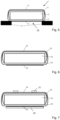
- Fig. 8 corresponds to Fig. 7 with added charges illustrating the charge distribution at the front side, on the back side and on the edge 19 of the hetero-junction solar cell 1, wherein in the example shown the semiconductor substrate 11 is n-doped, the at least one front layer 12 is p-doped and the at least one back layer 13 is n-doped.
- Fig. 9 schematically shows the stack of layers 11, 12, 13 present on the edge 19 of the hetero-junction solar cell 1 of Fig 8 .
- the horizontal structure n/(i)p/(i)n provided by the n-doped semiconductor substrate 11, the p-doped at least one front layer 12 (emitter) and the n-doped at least one back layer 13 (back surface field) acts as two diodes in opposition blocking a current flow in lateral direction. If the at least one back layer 13 would be formed prior to forming of the at least one front layer 12, that would lead to a shunt.
Landscapes
- Photovoltaic Devices (AREA)
Description
- The present invention relates to a method of manufacturing a hetero-junction solar cell, the solar cell having a front side for an incidence of light into the solar cell and a back side opposite to the front side. The method includes the steps of: providing a doped and textured semiconductor substrate, said semiconductor substrate having a front surface and a back surface opposite to each other and an edge surrounding the semiconductor substrate; forming at least one front layer on the front surface of the semiconductor substrate, wherein the at least one front layer covers at least a part of the edge of the semiconductor substrate, said at least one front layer containing semiconductor atoms or molecules being arranged in amorphous and/or microcrystalline and/or oxide and/or carbide phase, wherein said at least one front layer forms an emitter or a front surface field of the solar cell; forming at least one back layer on the back surface of the semiconductor substrate, said at least one back layer containing semiconductor atoms or molecules being arranged in amorphous and/or microcrystalline and/or oxide and/or carbide phase, wherein said at least one back layer forms a back surface field or a back emitter of the solar cell, and wherein the at least one front layer is formed prior to forming of the at least one back layer, and the at least one back layer covers at least a part of the edge of the semiconductor substrate and also covers at least a part of the at least one front layer that overlaps the edge of the semiconductor substrate; forming an electrically conductive anti-reflection coating on the at least one front layer, said anti-reflection coating covering the whole surface of the at least one front layer and being at least partially transparent to the light irradiating into the solar cell, wherein the anti-reflection coating covers at least a part of the at least one back layer overlapping the edge; forming an electrically conductive back coating on the at least one back layer; and forming a front grid metallization on the anti-reflection coating, wherein the conductive back coating is formed on the surface of the at least one back layer with a distance to the edge of the semiconductor substrate, leaving a merging region consisting of a margin area of the surface of the at least one back layer and the edge of the semiconductor substrate free from the conductive back coating, wherein there is no electrical contact between the conductive back coating and the conductive anti-reflection coating at all during the whole process of formation of the conductive back coating.
- Methods and accordant hetero-junction solar cells with of that type are known in different variants in the state of the art. Conventional hetero-junction solar cells are formed from an n-type doped substrate wherein a p-type doped emitter is formed on a front side of this substrate. That front side corresponds to the face where sun light mainly introduces into the solar cell. Fabrication of this type of solar cell involves deposition of the p-doped emitter layer on the front side of the substrate and deposition of an n-doped layer forming a back surface field on the back side of the substrate. In other solar cells, the type of doping used for the substrate and the doped layers can be the opposite way round. Moreover, it is also possible to place the emitter on the back side of the substrate and to form a front surface field layer on the front side of the substrate.
- To improve cell performances, intrinsic layers can be used between the substrate and the doped layers. The doped and intrinsic layers can be of any type of material. Most commonly, these layers are based on silicon in an amorphous and/or microcrystalline and/or oxide and/or carbide phase.
- In hetero-junction solar cells, it is necessary to prevent an electrical short circuit between the electrically conductive layers on the front and on the back side of the solar cell. Since such an undesired short circuit is typically formed around the edges, that means the side surfaces, of the semiconductor substrate used, the methods for preventing such short circuits are referred to as edge isolation methods. In the state of the art, there are different technologies knows to provide an edge isolation of hetero-junction solar cells.
- The document
US 5,935,344 A describes a method for edge isolation of hetero-junction solar cells using a structuring of the electrical conductive films on the front side or on the back side of the solar cell by laser drilling. In result of this structuring, a trench is formed at a peripheral portion of the front side or of the back side of the solar cell, the trench going at least through the respective transparent conductive film and the respective doped amorphous silicon layer. The trench surrounds continuously the laminated body of electrical conductive layers formed on the front side or on the back side of the solar cell. Alternatively, the document suggests to remove all deposited layers at the side surfaces of the substrate or to expose the side surfaces of the substrate at least partially by forming a continuous trench around the side surfaces of the substrate by laser irradiation. This technology includes the risk of creation of damages of the certain substrate regions and layers of the solar cell by the impact of the laser. Structuring of the front transparent conductive film, as it is suggested in one embodiment of this document, leads, moreover, to a decreased cell performance. - Another method of edge isolation of solar cells is disclosed in the document
WO 2012/059878 A1 . During manufacturing of the proposed solar cell, a narrow line of coating is applied along cell edge on one side or on both sides or on the edge of the solar cell prior to depositing electrically conductive films on the front and/or the back side of the solar cell. After the deposition of the conductive films, the narrow line of coating is removed by a wet or dry processing step. Thus, an interruption of the electrical conductive layers on the front and/or the back side of the solar cell can be realized for preventing of short circuits between the front and the back side of the solar cell. Although this method is very effective, it requires first a very sensible, local formation of the thin, narrow line at the edge of the substrate which is not easy to handle and second a removal of that narrow line being under the conductive film bearing the risk of an unintentional removal of further, alongside parts of the conductive film. - The document
JP 2006 222469 A - It is therefore the object of the present invention to provide an easy and low-cost method of manufacturing of a hetero-junction solar cell and an according solar cell, wherein short circuits between the front and the back side of the solar cell are prevented and the solar cell is not damaged by the method steps and shows good cell performance.
- This object is solved by a method of the above mentioned type, wherein said electrically conductive anti-reflection coating covers the whole surface of the at least one front layer and said electrically conductive anti-reflection coating covers at least a part of the edge of the semiconductor substrate..
- In the method of the present invention, already during the one step of forming the electrically conductive back coating all requirements for a prevention of short circuits between the front and the back side of the solar cell are fulfilled. By forming the electrically conductive back coating only in a middle part of the substrate leaving a margin to the edge of the substrate free, the conductive back coating does neither cover nor overlap over the side surfaces of the substrate and comes therefore not in contact with a conductive layer on the front side of the solar cell. The method of the present invention uses for this effect conventional process steps, like a deposition through a mask, which have no damaging influence on the solar cell substrate or its layers. The edge isolation method of the present invention can be easily implemented in the solar cell process flow without extra cost. Thus, an easy and low-cost but very reliable and effective method for edge isolation of hetero-junction solar cells can be provided by the present invention.
- The method of the present invention involves no structuring of the transparent conductive layer(s) on front of the solar cell. Without this front side structuring, the cell front area is larger and allows collecting more light and generating more current. Moreover, the uniform front transparent conductive film (anti-reflection coating) provides a better cell appearance for module integration.
- The edge isolation method of the present invention is only effective if the cell fabrication steps used are realized in a defined order. It is in particular advantageous if the at least one front layer is formed prior to forming of the at least one back layer. This sequence is not usual. If the formation of the at least one back layer would be performed before the formation of the at least one front layer, there would be a high risk of shunts on the cell edge.
- In a variant of the method of the present invention, the conductive back coating is formed with a distance of 5 µm to 10 mm from the edge of the semiconductor substrate.
- In a further improved embodiment of the present invention, the conductive back coating is formed with a distance of 30 µm to 3 mm from the edge of the semiconductor substrate.
- It is especially beneficial if the conductive back coating is deposited on the surface of the at least one back layer through a shadow mask having a opening being adapted to the dimensions of the semiconductor substrate, but smaller, and having a cover region around this opening covering at least the margin area of the surface of the at least one back layer during deposition. The physical mask covers this way the substrate's edge during the deposition of the conductive back coating. The mask is, for instance, able to protect few micrometers to millimeters to the cell edge from the film deposition. The mask can be easily integrated in a carrier holder of a deposition tool. With this method, edge isolation can be performed during the back side conductive film deposition without the need of an extra step to perform the edge isolation. This leads to a reduction of process steps reducing the final cell costs.
- In accordance with another option of the present invention, the conductive back coating is deposited on the whole surface of the at least one back layer, followed by a removal of a rim of the conductive back coating.
- The removal of the rim of the conductive back coating can be done by chemical etching and/or lift-off and/or laser ablation of the rim of the conductive back coating.
- By the method a hetero-junction solar cell with a front side for an incidence of light into the solar cell and a back side opposite to the front side is produced, the solar cell comprising: a doped and textured semiconductor substrate, said semiconductor substrate having a front surface and a back surface opposite to each other and an edge surrounding the semiconductor substrate; at least one front layer formed on the front surface of the semiconductor substrate, said at least one front layer containing semiconductor atoms or molecules being arranged in amorphous and/or microcrystalline and/or oxide and/or carbide phase; at least one back layer formed on the back surface of the semiconductor substrate, said at least one back layer containing semiconductor atoms or molecules being arranged in amorphous and/or microcrystalline and/or oxide and/or carbide phase; an electrically conductive anti-reflection coating formed on the at least one front layer, said anti-reflection coating covering the whole surface of the at least one front layer and being at least partially transparent to the light irradiating into the solar cell; an electrically conductive back coating formed on the at least one back layer; a front grid metallization formed on the anti-reflection coating; and a back electrode formed on the conductive back coating; wherein the conductive back coating is formed on the surface of the at least one back layer with a distance to the edge of the semiconductor substrate, leaving a merging region consisting of a margin area of the surface of the at least one back layer and the edge of the semiconductor substrate free from the conductive back coating, wherein there is no electrical contact between the conductive back coating and the conductive anti-reflection coating at all.
- The hetero-junction solar cell can be produced without structuring of the front transparent conductive film forming the anti-reflection coating of the solar cell. This allows better light collection and cell performances with a homogeneous front side appearance of the solar cell having no color gradient of the anti-reflection coating on the edge of the solar cell.
- In a favorable embodiment of the hetero-junction solar cell, the at least one back layer overlaps the at least one front layer. That leads to the effect that there is formed a horizontal structure of an n-/p-/n- or a p-/n-/p-layer-stack on the cell edge acting as two diodes in opposition that block current flow in lateral direction.
- Exemplarily, the conductive back coating has a distance of 5 µm to 10 mm from the edge of the semiconductor substrate. This results in a very sure electrical isolation of the front side and the back side of the hetero-junction solar cell of the present invention.
- A favorable embodiment of the method of the present invention is explained in the following with reference to the drawings in which
- Fig. 1
- schematically shows a semiconductor substrate used for manufacturing a hetero-junction solar cell in accordance with the present invention in a sectional view;
- Fig. 2
- schematically shows the substrate of
Fig. 1 being covered by at least one front layer on a front surface of the semiconductor substrate; - Fig. 3
- schematically shows the structure of
Fig. 2 being covered by at least one back layer on a back surface of the semiconductor substrate; - Fig. 4
- schematically shows the structure of
Fig. 3 being coated by an electrically conductive anti-reflection coating formed on the at least one front layer; - Fig. 5
- schematically shows the structure of
Fig. 4 wherein an electrically conductive back coating is deposited through a mask on the at least one back layer; - Fig. 6
- schematically shows the structure of
Fig. 5 with removed mask; - Fig. 7
- schematically shows a hetero-junction solar cell being formed from the structure of
Fig. 6 plus forming a front grid metallization and a back electrode; - Fig. 8
- corresponds to
Fig. 7 with added charges illustrating the charge distribution at the front side, on the back side and on the edge of the hetero-junction solar cell; and - Fig. 9
- schematically shows the stack of layers present on the edge of the heterojunction solar cell of
Fig. 8 . -
Figs. 1 to 7 schematically show an advantageous sequence of process steps of the method of the present invention resulting in a hetero-junctionsolar cell 1. The steps shown in theFigs. 1 to 7 are only representative figures showing characteristic but not all details of the process used. - As shown in
Fig. 1 , the method of the present invention starts with asemiconductor substrate 11. Thesemiconductor substrate 11 can consist of any semiconductive material that can have any size and doping. Thesemiconductor substrate 11 is in the embodiment shown of a crystalline semiconductor material, preferably of monocrystalline or multi-crystalline silicon. Thesemiconductor substrate 11 is doped. The doping can be of n-type or of p-type, dependent from the kind of solar cell to be produced. Thesemiconductor substrate 11 has afront surface 17 for an incidence of most of the light and aback surface 18 opposite to thefront surface 17. Thefront surface 17 of thesemiconductor substrate 11 is textured to decrease a reflection of light received. Moreover, thesemiconductor substrate 11 has anedge 19 surrounding the bulk of thesemiconductor substrate 11 and extending between thefront surface 17 and theback surface 18 of thesemiconductor substrate 11. Theedge 19 is only schematically shown and is not necessarily flat as shown inFig. 1 , but can also be convex or pointed. As usual in semiconductor technologies, thesemiconductor substrate 11 is cleaned. Cleaning steps are made before and/or after the following method steps, too, and are not especially mentioned in each case. - With reference to
Fig. 2 , in a next step of the method of the present invention, at least onefront layer 12 is formed on thefront surface 17 of thesemiconductor substrate 11. The at least onefront layer 12 can be one layer or a stack of layers. The at least onefront layer 12 covers at least a part of theedge 19 of thesemiconductor substrate 11. The at least onefront layer 12 contains semiconductor atoms or molecules being arranged in amorphous and/or microcrystalline and/or oxide and/or carbide phase. For instance, the at least onefront layer 12 can consist of an intrinsic silicon layer formed directly on thefront surface 17 of thesemiconductor substrate 11 and a doped amorphous silicon layer, such as a p-doped amorphous silicon layer, formed on the intrinsic layer. In other embodiments of the invention, that intrinsic layer can be omitted. The at least onefront layer 12 is preferably deposited by PECVD (plasma enhanced physical vapor deposition). The at least onefront layer 12 has typically a thickness of less than 50 nm. Depending on the type of solar cell to be produced, the at least onefront layer 12 will form an emitter or a front surface field of the solar cell. - As demonstrated in
Fig. 3 , in a further step of the method of the present invention, at least oneback layer 13 is formed on theback surface 18 of thesemiconductor substrate 11. In the shown embodiment of the method of the present invention, the at least oneback layer 13 is explicitly formed after the formation of the at least onefront layer 12. The at least oneback layer 13 can be one layer or a stack of layers. The at least oneback layer 13 is preferably deposited by PECVD (plasma enhanced physical vapor deposition). The at least oneback layer 13 has typically a thickness of less than 50 nm. The at least oneback layer 13 covers at least a part of theedge 19 of thesemiconductor substrate 11 and also covers at least a part of the at least onefront layer 12 that overlaps theedge 19 of thesemiconductor substrate 11. - The at least one
back layer 13 contains semiconductor atoms or molecules being arranged in amorphous and/or microcrystalline and/or oxide and/or carbide phase. For instance, the at least oneback layer 13 can consist of an intrinsic silicon layer formed directly on theback surface 18 of thesemiconductor substrate 11 and a doped amorphous silicon layer, such as an n+-doped amorphous silicon layer, formed on the intrinsic layer. In other embodiments of the invention, that intrinsic layer can be omitted. Depending on the type of solar cell to be produced, the at least oneback layer 13 will form a back surface field or a back emitter. - In the method step shown in
Fig. 4 , an electrically conductiveanti-reflection coating 14 is formed on the at least onefront layer 12. Theanti-reflection coating 14 is at least partially transparent to the light irradiating into the solar cell. For instance, many transparent conductive oxides, such as indium oxide or indium tin oxide, can be used as material for theanti-reflection coating 14. Theanti-reflection coating 14 covers at least the whole surface of the at least onefront layer 12. Theanti-reflection coating 14 also covers at least a part of theedge 19 of thesemiconductor substrate 11 and at least a part of the at least oneback layer 13 overlapping theedge 19 and at least a part of the at least onefront layer 12 overlapping theedge 19. - Since, as mentioned above, the
edge 19 of thesemiconductor substrate 11 can be covered with a variable combination of layers being part of the at least onefront layer 12 and/or the at least oneback layer 13 and/or theanti-reflection coating 14, in the following as well as in the claims the expression "edge 19" should be understood as to be the whole surrounding side surface(s) of thesemiconductor substrate 11 with and/or without these additional layers or parts of layers. - In a next step of the method of the present invention shown in
Fig. 5 , amask 16 is provided on the back side of the structure. Themask 16 is a shadow mask has a cover region that covers theedge 19 of thesemiconductor substrate 11 as well as a margin of the at least oneback layer 13. In its middle region, the mask has anopening 20. The shape of theopening 20 is adapted to the shape of thesemiconductor substrate 11, but has smaller dimensions. The margin can, for instance, have a radial dimension of a few micrometers to a few millimeters, such as of about 5 µm to about 10 mm, preferably of about 30 µm to 3 mm, measured from theedge 19 of thesemiconductor substrate 11. Through theopening 20 of themask 16, an electricallyconductive back coating 15 is deposited on the surface of the at least oneback layer 13. Due to themask 16, the electricallyconductive back coating 15 is formed only on the surface of the at least oneback layer 13 with a distance to theedge 19 of thesemiconductor substrate 11, leaving a merging region consisting of a margin area of the surface of the at least oneback layer 13 and theedge 19 of thesemiconductor substrate 11 free from theconductive back coating 15. There is no electrical contact between theconductive back coating 15 and the conductiveanti-reflection coating 14 at all during the whole process of formation of theconductive back coating 15. The area covered by theconductive back coating 15 should be maximized without being in contact with theanti-reflection coating 14. - The
anti-reflection coating 14 and theconductive back coating 15 can be deposited in any order or at the same time. - The
conductive back coating 15 can be formed by transparent conductive film(s) and/or metallic film(s). Theconductive back coating 15 film(s) can be deposited by sputtering or evaporation techniques. - In other embodiments of the present invention, the step of
Fig. 5 can be replaced by two sub-steps wherein in a first sub-step theconductive back coating 15 is deposited on the surface of the at least oneback layer 13. During deposition of the conductive back-coating 15, an electrical contact between theconductive back coating 15 and theanti-reflection coating 14 has to be avoided. In a second sub-step, a rim of theconductive back coating 15 is removed. The removal of that rim of theconductive back coating 15 can be done by chemical etching and/or lift-off of the rim and/or laser ablation. -
Fig. 6 schematically shows the structure ofFig. 5 after removal of themask 16. - As schematically shown in
Fig. 7 , the method of manufacturing a hetero-junctionsolar cell 1 in according with the present invention ends with forming afront grid metallization 21. In some cases, in an additional step, aback electrode 22 is formed by a metallization of the back side of theconductive back coating 15. -
Fig. 8 corresponds toFig. 7 with added charges illustrating the charge distribution at the front side, on the back side and on theedge 19 of the hetero-junctionsolar cell 1, wherein in the example shown thesemiconductor substrate 11 is n-doped, the at least onefront layer 12 is p-doped and the at least oneback layer 13 is n-doped. -
Fig. 9 schematically shows the stack oflayers edge 19 of the hetero-junctionsolar cell 1 ofFig 8 . The horizontal structure n/(i)p/(i)n provided by the n-dopedsemiconductor substrate 11, the p-doped at least one front layer 12 (emitter) and the n-doped at least one back layer 13 (back surface field) acts as two diodes in opposition blocking a current flow in lateral direction. If the at least oneback layer 13 would be formed prior to forming of the at least onefront layer 12, that would lead to a shunt.
Claims (6)
- Method of manufacturing a hetero-junction solar cell (1), the solar cell (1) comprising a front side for an incidence of light into the solar cell (1) and a back side opposite to the front side, the method including the steps of- providing a doped and textured semiconductor substrate (11), said semiconductor substrate (11) having a front surface (17) and a back surface (18) opposite to each other and an edge (19) surrounding the semiconductor substrate (11);- forming at least one front layer (12) on the front surface (17) of the semiconductor substrate (11), wherein the at least one front layer (12) covers at least a part of the edge (19) of the semiconductor substrate (11), said at least one front layer (12) containing semiconductor atoms or molecules being arranged in amorphous and/or microcrystalline and/or oxide and/or carbide phase, wherein said at least one front layer (12) forms an emitter or a front surface field of the solar cell (1);- forming at least one back layer (13) on the back surface (18) of the semiconductor substrate (11), said at least one back layer (13) containing semiconductor atoms or molecules being arranged in amorphous and/or microcrystalline and/or oxide and/or carbide phase, wherein said at least one back layer (13) forms a back surface field or a back emitter of the solar cell (1), and wherein the at least one front layer (12) is formed prior to forming of the at least one back layer (13), and the at least one back layer (13) covers at least a part of the edge of the semiconductor substrate (11) and also covers at least a part of the at least one front layer (12) that overlaps the edge of the semiconductor substrate (11);- forming an electrically conductive anti-reflection coating (14) on the at least one front layer (12), said anti-reflection coating (14) being at least partially transparent to the light irradiating into the solar cell (1), wherein the anti-reflection coating (14) covers at least a part of the at least one back layer (13) overlapping the edge (19);- forming an electrically conductive back coating (15) on the at least one back layer (13); and- forming a front grid metallization (21) on the anti-reflection coating (14);wherein the conductive back coating (15) is formed on the surface of the at least one back layer (13) with a distance to the edge (19) of the semiconductor substrate (11), leaving a margin area of the surface of the at least one back layer (13) and the edge (19) of the semiconductor substrate (11) free from the conductive back coating (15), wherein there is no electrical contact between the conductive back coating (15) and the conductive anti-reflection coating (14) at all during the whole process of formation of the conductive back coating (15),wherein said electrically conductive anti-reflection coating (14) covers the whole surface of the at least one front layer (12), characterized in that the electrically conductive anti-reflection coating (14) covers at least a part of the edge (19) of the semiconductor substrate (11).
- Method of claim 1, wherein the conductive back coating (15) is formed with a distance of 5 µm to 10 mm from the edge (19) of the semiconductor substrate (11).
- Method of claim 2, wherein the conductive back coating (15) is formed with a distance of 30 µm to 3 mm from the edge (19) of the semiconductor substrate (11).
- Method of at least one of the preceding claims, wherein the conductive back coating (15) is deposited on the surface of the at least one back layer (13) through a shadow mask (16) having a opening (20) being adapted to the dimensions of the semiconductor substrate (11), but smaller, and having a cover region around this opening (20) covering at least the margin area of the surface of the at least one back layer (13) during deposition.
- Method of at least one of the claims 1 to 3, wherein the conductive back coating (15) is deposited on the whole surface of the at least one back layer (13), followed by a removal of a rim of the conductive back coating (15).
- Method of claim 5, wherein the removal of the rim of the conductive back coating (15) is done by chemical etching and/or lift-off and/or laser ablation of the rim of the conductive back coating (15).
Priority Applications (5)
| Application Number | Priority Date | Filing Date | Title |
|---|---|---|---|
| PL21150107.7T PL3832737T3 (en) | 2012-07-02 | 2012-07-02 | Method of manufacturing a hetero-junction solar cell |
| ES21150107T ES3005058T3 (en) | 2012-07-02 | 2012-07-02 | Method of manufacturing a hetero-junction solar cell |
| EP21150107.7A EP3832737B1 (en) | 2012-07-02 | 2012-07-02 | Method of manufacturing a hetero-junction solar cell |
| HUE21150107A HUE069227T2 (en) | 2012-07-02 | 2012-07-02 | Method of manufacturing a hetero-junction solar cell |
| EP24179874.3A EP4404282A3 (en) | 2012-07-02 | 2012-07-02 | Method of manufacturing a hetero-junction solar cell |
Applications Claiming Priority (2)
| Application Number | Priority Date | Filing Date | Title |
|---|---|---|---|
| EP21150107.7A EP3832737B1 (en) | 2012-07-02 | 2012-07-02 | Method of manufacturing a hetero-junction solar cell |
| EP12004905.1A EP2682990B2 (en) | 2012-07-02 | 2012-07-02 | Methods of manufacturing hetero-junction solar cells with edge isolation |
Related Parent Applications (2)
| Application Number | Title | Priority Date | Filing Date |
|---|---|---|---|
| EP12004905.1A Division EP2682990B2 (en) | 2012-07-02 | 2012-07-02 | Methods of manufacturing hetero-junction solar cells with edge isolation |
| EP12004905.1A Division-Into EP2682990B2 (en) | 2012-07-02 | 2012-07-02 | Methods of manufacturing hetero-junction solar cells with edge isolation |
Related Child Applications (2)
| Application Number | Title | Priority Date | Filing Date |
|---|---|---|---|
| EP24179874.3A Division-Into EP4404282A3 (en) | 2012-07-02 | 2012-07-02 | Method of manufacturing a hetero-junction solar cell |
| EP24179874.3A Division EP4404282A3 (en) | 2012-07-02 | 2012-07-02 | Method of manufacturing a hetero-junction solar cell |
Publications (3)
| Publication Number | Publication Date |
|---|---|
| EP3832737A1 EP3832737A1 (en) | 2021-06-09 |
| EP3832737B1 true EP3832737B1 (en) | 2024-09-04 |
| EP3832737C0 EP3832737C0 (en) | 2024-09-04 |
Family
ID=46506114
Family Applications (3)
| Application Number | Title | Priority Date | Filing Date |
|---|---|---|---|
| EP24179874.3A Pending EP4404282A3 (en) | 2012-07-02 | 2012-07-02 | Method of manufacturing a hetero-junction solar cell |
| EP12004905.1A Active EP2682990B2 (en) | 2012-07-02 | 2012-07-02 | Methods of manufacturing hetero-junction solar cells with edge isolation |
| EP21150107.7A Active EP3832737B1 (en) | 2012-07-02 | 2012-07-02 | Method of manufacturing a hetero-junction solar cell |
Family Applications Before (2)
| Application Number | Title | Priority Date | Filing Date |
|---|---|---|---|
| EP24179874.3A Pending EP4404282A3 (en) | 2012-07-02 | 2012-07-02 | Method of manufacturing a hetero-junction solar cell |
| EP12004905.1A Active EP2682990B2 (en) | 2012-07-02 | 2012-07-02 | Methods of manufacturing hetero-junction solar cells with edge isolation |
Country Status (4)
| Country | Link |
|---|---|
| EP (3) | EP4404282A3 (en) |
| ES (2) | ES3005058T3 (en) |
| HU (1) | HUE069227T2 (en) |
| PL (1) | PL3832737T3 (en) |
Families Citing this family (14)
| Publication number | Priority date | Publication date | Assignee | Title |
|---|---|---|---|---|
| HUE069227T2 (en) | 2012-07-02 | 2025-02-28 | Meyer Burger Germany Gmbh | Method of manufacturing a hetero-junction solar cell |
| WO2015068340A1 (en) * | 2013-11-08 | 2015-05-14 | パナソニックIpマネジメント株式会社 | Solar cell |
| WO2015178307A1 (en) * | 2014-05-23 | 2015-11-26 | シャープ株式会社 | Photoelectric conversion element |
| JP6650407B2 (en) * | 2014-09-30 | 2020-02-19 | 株式会社カネカ | Method of manufacturing solar cell and method of manufacturing solar cell module |
| CN105810770B (en) * | 2014-12-30 | 2017-10-03 | 新日光能源科技股份有限公司 | heterojunction solar cell and manufacturing method thereof |
| FR3038143B1 (en) | 2015-06-26 | 2017-07-21 | Commissariat Energie Atomique | METHOD OF ISOLATING THE EDGES OF A HETEROJUNCTION PHOTOVOLTAIC CELL |
| KR101778128B1 (en) | 2016-01-20 | 2017-09-13 | 엘지전자 주식회사 | Solar cell |
| WO2019182243A1 (en) * | 2018-03-19 | 2019-09-26 | 엘지전자 주식회사 | Solar cell and method for manufacturing same |
| DE102019123785A1 (en) | 2019-09-05 | 2021-03-11 | Meyer Burger (Germany) Gmbh | Rear-side emitter solar cell structure with a heterojunction, as well as method and apparatus for producing the same |
| DE102019123758A1 (en) | 2019-09-05 | 2021-03-11 | Schaeffler Technologies AG & Co. KG | Wave gear for variable valve control of an internal combustion engine |
| CN111755574A (en) * | 2020-07-27 | 2020-10-09 | 苏州联诺太阳能科技有限公司 | Double-sided solar cell and preparation method thereof |
| EP4068393A1 (en) | 2021-03-31 | 2022-10-05 | Meyer Burger Research AG | Method for manufacturing solar cells and solar module |
| CN116273670B (en) * | 2023-02-28 | 2024-07-19 | 武汉鑫誉金天科技有限公司 | Solar cell coating apparatus |
| WO2026050345A1 (en) * | 2024-08-29 | 2026-03-05 | Corning Incorporated | Heterojunction photovoltaic cell and method of making the same |
Citations (28)
| Publication number | Priority date | Publication date | Assignee | Title |
|---|---|---|---|---|
| EP0881694A1 (en) | 1997-05-30 | 1998-12-02 | Interuniversitair Micro-Elektronica Centrum Vzw | Solar cell and process of manufacturing the same |
| US5935344A (en) | 1995-10-26 | 1999-08-10 | Sanyo Electric Co., Ltd. | Photovoltaic element and manufacturing method thereof |
| JPH11251609A (en) | 1998-03-05 | 1999-09-17 | Sanyo Electric Co Ltd | Photovoltaic element and its manufacture |
| JPH11261086A (en) | 1998-03-12 | 1999-09-24 | Sharp Corp | Photovoltaic device and solar cell module |
| WO2000055923A1 (en) | 1999-03-17 | 2000-09-21 | Ebara Solar, Inc. | An aluminum alloy back junction solar cell and a process for fabrication thereof |
| JP2001044461A (en) | 1999-07-26 | 2001-02-16 | Sanyo Electric Co Ltd | Photovoltaic element and method for manufacturing the same |
| JP2002076397A (en) | 2000-08-29 | 2002-03-15 | Sanyo Electric Co Ltd | Manufacturing method of photovoltaic device |
| JP2004140087A (en) | 2002-10-16 | 2004-05-13 | Canon Inc | Polycrystalline silicon substrate for solar cell, method of manufacturing the same, and method of manufacturing solar cell using this substrate |
| JP2004221437A (en) | 2003-01-17 | 2004-08-05 | Sanyo Electric Co Ltd | Photovoltaic device and manufacturing method thereof |
| JP2004296550A (en) | 2003-03-25 | 2004-10-21 | Sanyo Electric Co Ltd | Photovoltaic element and its fabricating process |
| JP2005260149A (en) | 2004-03-15 | 2005-09-22 | Sanyo Electric Co Ltd | Method of manufacturing photovoltaic device |
| JP2006222469A (en) * | 2006-05-29 | 2006-08-24 | Sanyo Electric Co Ltd | Photosensor |
| EP1881534A2 (en) | 2006-07-20 | 2008-01-23 | Sanyo Electric Co., Ltd. | Solar cell module |
| JP2008305945A (en) | 2007-06-07 | 2008-12-18 | Kaneka Corp | Substrate for thin film solar cell and manufacturing method of the same, and manufacturing method of thin film solar cell |
| EP2043161A2 (en) | 2007-09-28 | 2009-04-01 | Sanyo Electric Co., Ltd. | Solar cell, solar cell module, and method of manufacturing the solar cell |
| US20090151782A1 (en) | 2007-12-18 | 2009-06-18 | Lg Electronics Inc. | Hetero-junction silicon solar cell and fabrication method thereof |
| JP2009290234A (en) | 2009-09-07 | 2009-12-10 | Sanyo Electric Co Ltd | Photovoltaic element |
| JP2010080885A (en) | 2008-09-29 | 2010-04-08 | Sanyo Electric Co Ltd | Method for producing solar cell |
| WO2010081460A1 (en) | 2009-01-16 | 2010-07-22 | Q-Cells Se | Solar cell and method for producing a solar cell |
| WO2010118479A1 (en) | 2009-04-17 | 2010-10-21 | Transform Solar Pty Ltd | Elongate solar cell and edge contact |
| WO2010118688A1 (en) | 2009-04-15 | 2010-10-21 | Zhu Huilong | Thin film of solar battery structure, thin film of solar battery array and manufacturing method thereof |
| JP2011023758A (en) | 2010-11-02 | 2011-02-03 | Sanyo Electric Co Ltd | Method of manufacturing photovoltaic element |
| JP2011035092A (en) | 2009-07-31 | 2011-02-17 | Sanyo Electric Co Ltd | Back-junction type solar cell and solar cell module using the same |
| JP2011060971A (en) | 2009-09-09 | 2011-03-24 | Kaneka Corp | Crystal silicon solar cell and method of manufacturing the same |
| WO2011040489A1 (en) | 2009-09-29 | 2011-04-07 | 京セラ株式会社 | Solar cell element and solar cell module |
| JP2011187906A (en) | 2010-02-15 | 2011-09-22 | Kyocera Corp | Solar cell element and method of manufacturing the same |
| US20120048371A1 (en) | 2010-08-25 | 2012-03-01 | Wonseok Choi | Solar cell and method for manufacturing the same |
| US20120145233A1 (en) | 2010-10-11 | 2012-06-14 | Lg Electronics Inc. | Back contact solar cell and manufacturing method thereof |
Family Cites Families (5)
| Publication number | Priority date | Publication date | Assignee | Title |
|---|---|---|---|---|
| JP4194379B2 (en) * | 2003-01-22 | 2008-12-10 | 三洋電機株式会社 | Photovoltaic device |
| EP1555695B1 (en) * | 2004-01-13 | 2011-05-04 | Sanyo Electric Co., Ltd. | Photovoltaic device |
| ES2385720T3 (en) * | 2005-02-25 | 2012-07-30 | Sanyo Electric Co., Ltd. | Photovoltaic cell |
| EP2450970A1 (en) * | 2010-11-05 | 2012-05-09 | Roth & Rau AG | Edge isolation by lift-off |
| HUE069227T2 (en) | 2012-07-02 | 2025-02-28 | Meyer Burger Germany Gmbh | Method of manufacturing a hetero-junction solar cell |
-
2012
- 2012-07-02 HU HUE21150107A patent/HUE069227T2/en unknown
- 2012-07-02 ES ES21150107T patent/ES3005058T3/en active Active
- 2012-07-02 EP EP24179874.3A patent/EP4404282A3/en active Pending
- 2012-07-02 PL PL21150107.7T patent/PL3832737T3/en unknown
- 2012-07-02 EP EP12004905.1A patent/EP2682990B2/en active Active
- 2012-07-02 ES ES12004905T patent/ES2873473T5/en active Active
- 2012-07-02 EP EP21150107.7A patent/EP3832737B1/en active Active
Patent Citations (28)
| Publication number | Priority date | Publication date | Assignee | Title |
|---|---|---|---|---|
| US5935344A (en) | 1995-10-26 | 1999-08-10 | Sanyo Electric Co., Ltd. | Photovoltaic element and manufacturing method thereof |
| EP0881694A1 (en) | 1997-05-30 | 1998-12-02 | Interuniversitair Micro-Elektronica Centrum Vzw | Solar cell and process of manufacturing the same |
| JPH11251609A (en) | 1998-03-05 | 1999-09-17 | Sanyo Electric Co Ltd | Photovoltaic element and its manufacture |
| JPH11261086A (en) | 1998-03-12 | 1999-09-24 | Sharp Corp | Photovoltaic device and solar cell module |
| WO2000055923A1 (en) | 1999-03-17 | 2000-09-21 | Ebara Solar, Inc. | An aluminum alloy back junction solar cell and a process for fabrication thereof |
| JP2001044461A (en) | 1999-07-26 | 2001-02-16 | Sanyo Electric Co Ltd | Photovoltaic element and method for manufacturing the same |
| JP2002076397A (en) | 2000-08-29 | 2002-03-15 | Sanyo Electric Co Ltd | Manufacturing method of photovoltaic device |
| JP2004140087A (en) | 2002-10-16 | 2004-05-13 | Canon Inc | Polycrystalline silicon substrate for solar cell, method of manufacturing the same, and method of manufacturing solar cell using this substrate |
| JP2004221437A (en) | 2003-01-17 | 2004-08-05 | Sanyo Electric Co Ltd | Photovoltaic device and manufacturing method thereof |
| JP2004296550A (en) | 2003-03-25 | 2004-10-21 | Sanyo Electric Co Ltd | Photovoltaic element and its fabricating process |
| JP2005260149A (en) | 2004-03-15 | 2005-09-22 | Sanyo Electric Co Ltd | Method of manufacturing photovoltaic device |
| JP2006222469A (en) * | 2006-05-29 | 2006-08-24 | Sanyo Electric Co Ltd | Photosensor |
| EP1881534A2 (en) | 2006-07-20 | 2008-01-23 | Sanyo Electric Co., Ltd. | Solar cell module |
| JP2008305945A (en) | 2007-06-07 | 2008-12-18 | Kaneka Corp | Substrate for thin film solar cell and manufacturing method of the same, and manufacturing method of thin film solar cell |
| EP2043161A2 (en) | 2007-09-28 | 2009-04-01 | Sanyo Electric Co., Ltd. | Solar cell, solar cell module, and method of manufacturing the solar cell |
| US20090151782A1 (en) | 2007-12-18 | 2009-06-18 | Lg Electronics Inc. | Hetero-junction silicon solar cell and fabrication method thereof |
| JP2010080885A (en) | 2008-09-29 | 2010-04-08 | Sanyo Electric Co Ltd | Method for producing solar cell |
| WO2010081460A1 (en) | 2009-01-16 | 2010-07-22 | Q-Cells Se | Solar cell and method for producing a solar cell |
| WO2010118688A1 (en) | 2009-04-15 | 2010-10-21 | Zhu Huilong | Thin film of solar battery structure, thin film of solar battery array and manufacturing method thereof |
| WO2010118479A1 (en) | 2009-04-17 | 2010-10-21 | Transform Solar Pty Ltd | Elongate solar cell and edge contact |
| JP2011035092A (en) | 2009-07-31 | 2011-02-17 | Sanyo Electric Co Ltd | Back-junction type solar cell and solar cell module using the same |
| JP2009290234A (en) | 2009-09-07 | 2009-12-10 | Sanyo Electric Co Ltd | Photovoltaic element |
| JP2011060971A (en) | 2009-09-09 | 2011-03-24 | Kaneka Corp | Crystal silicon solar cell and method of manufacturing the same |
| WO2011040489A1 (en) | 2009-09-29 | 2011-04-07 | 京セラ株式会社 | Solar cell element and solar cell module |
| JP2011187906A (en) | 2010-02-15 | 2011-09-22 | Kyocera Corp | Solar cell element and method of manufacturing the same |
| US20120048371A1 (en) | 2010-08-25 | 2012-03-01 | Wonseok Choi | Solar cell and method for manufacturing the same |
| US20120145233A1 (en) | 2010-10-11 | 2012-06-14 | Lg Electronics Inc. | Back contact solar cell and manufacturing method thereof |
| JP2011023758A (en) | 2010-11-02 | 2011-02-03 | Sanyo Electric Co Ltd | Method of manufacturing photovoltaic element |
Also Published As
| Publication number | Publication date |
|---|---|
| ES2873473T5 (en) | 2024-06-07 |
| ES3005058T3 (en) | 2025-03-13 |
| ES2873473T3 (en) | 2021-11-03 |
| HUE069227T2 (en) | 2025-02-28 |
| EP2682990B1 (en) | 2021-03-24 |
| PL3832737T3 (en) | 2025-01-07 |
| EP2682990A1 (en) | 2014-01-08 |
| EP3832737C0 (en) | 2024-09-04 |
| EP3832737A1 (en) | 2021-06-09 |
| EP4404282A3 (en) | 2024-10-23 |
| EP4404282A2 (en) | 2024-07-24 |
| EP2682990B2 (en) | 2023-11-22 |
Similar Documents
| Publication | Publication Date | Title |
|---|---|---|
| EP2682990B1 (en) | Hetero-junction solar cells with edge isolation and methods of manufacturing same | |
| EP2380203B1 (en) | Solar cell | |
| JP2024097088A (en) | Highly efficient solar cell structure and method of manufacture | |
| US5401336A (en) | Photovoltaic device | |
| US9006564B2 (en) | Method of manufacturing solar cell and solar cell | |
| US8962373B2 (en) | Hybrid polysilicon heterojunction back contact cell | |
| CN117954509B (en) | Preparation method of back contact solar cell, solar cell and cell assembly | |
| TWI559563B (en) | Hybrid polycrystalline germanium heterojunction back contact battery | |
| US8101852B2 (en) | Single-sided contact solar cell with plated- through holes and method for its production | |
| CN118248748A (en) | Back contact solar cell, preparation method and solar cell assembly | |
| JP2011507246A (en) | Back electrode type solar cell having wide backside emitter region and method for manufacturing the same | |
| CN118248749B (en) | Back contact solar cell, preparation method and battery assembly | |
| US20120000506A1 (en) | Photovoltaic module and method of manufacturing the same | |
| EP2380205B1 (en) | Solar cell | |
| US20170117433A1 (en) | A hybrid all-back-contact solar cell and method of fabricating the same | |
| TW201318030A (en) | Semiconductor light detecting device and method of preparing same | |
| WO2016203013A1 (en) | Method for producing a heterojunction photovoltaic cell | |
| CN102197491B (en) | Method for local contacting and local doping of semiconductor layers | |
| US10361321B2 (en) | Method of forming a contact for a photovoltaic cell | |
| JP2014072210A (en) | Photoelectric conversion element | |
| KR101179949B1 (en) | Solar cell | |
| JPH11177109A (en) | Solar cell | |
| CN121174690A (en) | Back contact solar cell, preparation method thereof and back contact solar cell module |
Legal Events
| Date | Code | Title | Description |
|---|---|---|---|
| PUAI | Public reference made under article 153(3) epc to a published international application that has entered the european phase |
Free format text: ORIGINAL CODE: 0009012 |
|
| STAA | Information on the status of an ep patent application or granted ep patent |
Free format text: STATUS: THE APPLICATION HAS BEEN PUBLISHED |
|
| AC | Divisional application: reference to earlier application |
Ref document number: 2682990 Country of ref document: EP Kind code of ref document: P |
|
| AK | Designated contracting states |
Kind code of ref document: A1 Designated state(s): AL AT BE BG CH CY CZ DE DK EE ES FI FR GB GR HR HU IE IS IT LI LT LU LV MC MK MT NL NO PL PT RO RS SE SI SK SM TR |
|
| STAA | Information on the status of an ep patent application or granted ep patent |
Free format text: STATUS: REQUEST FOR EXAMINATION WAS MADE |
|
| 17P | Request for examination filed |
Effective date: 20210917 |
|
| RBV | Designated contracting states (corrected) |
Designated state(s): AL AT BE BG CH CY CZ DE DK EE ES FI FR GB GR HR HU IE IS IT LI LT LU LV MC MK MT NL NO PL PT RO RS SE SI SK SM TR |
|
| TPAC | Observations filed by third parties |
Free format text: ORIGINAL CODE: EPIDOSNTIPA |
|
| STAA | Information on the status of an ep patent application or granted ep patent |
Free format text: STATUS: EXAMINATION IS IN PROGRESS |
|
| 17Q | First examination report despatched |
Effective date: 20221004 |
|
| GRAP | Despatch of communication of intention to grant a patent |
Free format text: ORIGINAL CODE: EPIDOSNIGR1 |
|
| STAA | Information on the status of an ep patent application or granted ep patent |
Free format text: STATUS: GRANT OF PATENT IS INTENDED |
|
| INTG | Intention to grant announced |
Effective date: 20240207 |
|
| GRAS | Grant fee paid |
Free format text: ORIGINAL CODE: EPIDOSNIGR3 |
|
| GRAA | (expected) grant |
Free format text: ORIGINAL CODE: 0009210 |
|
| STAA | Information on the status of an ep patent application or granted ep patent |
Free format text: STATUS: THE PATENT HAS BEEN GRANTED |
|
| AC | Divisional application: reference to earlier application |
Ref document number: 2682990 Country of ref document: EP Kind code of ref document: P |
|
| AK | Designated contracting states |
Kind code of ref document: B1 Designated state(s): AL AT BE BG CH CY CZ DE DK EE ES FI FR GB GR HR HU IE IS IT LI LT LU LV MC MK MT NL NO PL PT RO RS SE SI SK SM TR |
|
| REG | Reference to a national code |
Ref country code: GB Ref legal event code: FG4D |
|
| REG | Reference to a national code |
Ref country code: CH Ref legal event code: EP |
|
| REG | Reference to a national code |
Ref country code: IE Ref legal event code: FG4D |
|
| REG | Reference to a national code |
Ref country code: DE Ref legal event code: R096 Ref document number: 602012081054 Country of ref document: DE |
|
| 111Z | Information provided on other rights and legal means of execution |
Free format text: AL AT BE BG CH CY CZ DE DK EE ES FI FR GB GR HR HU IE IS IT LT LU LV MC MK MT NL NO PL PT RO RS SE SI SK SM TR Effective date: 20240618 |
|
| U01 | Request for unitary effect filed |
Effective date: 20240920 |
|
| U07 | Unitary effect registered |
Designated state(s): AT BE BG DE DK EE FI FR IT LT LU LV MT NL PT RO SE SI Effective date: 20241014 |
|
| PG25 | Lapsed in a contracting state [announced via postgrant information from national office to epo] |
Ref country code: NO Free format text: LAPSE BECAUSE OF FAILURE TO SUBMIT A TRANSLATION OF THE DESCRIPTION OR TO PAY THE FEE WITHIN THE PRESCRIBED TIME-LIMIT Effective date: 20241204 |
|
| PG25 | Lapsed in a contracting state [announced via postgrant information from national office to epo] |
Ref country code: GR Free format text: LAPSE BECAUSE OF FAILURE TO SUBMIT A TRANSLATION OF THE DESCRIPTION OR TO PAY THE FEE WITHIN THE PRESCRIBED TIME-LIMIT Effective date: 20241205 |
|
| PG25 | Lapsed in a contracting state [announced via postgrant information from national office to epo] |
Ref country code: HR Free format text: LAPSE BECAUSE OF FAILURE TO SUBMIT A TRANSLATION OF THE DESCRIPTION OR TO PAY THE FEE WITHIN THE PRESCRIBED TIME-LIMIT Effective date: 20240904 |
|
| PG25 | Lapsed in a contracting state [announced via postgrant information from national office to epo] |
Ref country code: RS Free format text: LAPSE BECAUSE OF FAILURE TO SUBMIT A TRANSLATION OF THE DESCRIPTION OR TO PAY THE FEE WITHIN THE PRESCRIBED TIME-LIMIT Effective date: 20241204 |
|
| PG25 | Lapsed in a contracting state [announced via postgrant information from national office to epo] |
Ref country code: RS Free format text: LAPSE BECAUSE OF FAILURE TO SUBMIT A TRANSLATION OF THE DESCRIPTION OR TO PAY THE FEE WITHIN THE PRESCRIBED TIME-LIMIT Effective date: 20241204 Ref country code: NO Free format text: LAPSE BECAUSE OF FAILURE TO SUBMIT A TRANSLATION OF THE DESCRIPTION OR TO PAY THE FEE WITHIN THE PRESCRIBED TIME-LIMIT Effective date: 20241204 Ref country code: HR Free format text: LAPSE BECAUSE OF FAILURE TO SUBMIT A TRANSLATION OF THE DESCRIPTION OR TO PAY THE FEE WITHIN THE PRESCRIBED TIME-LIMIT Effective date: 20240904 Ref country code: GR Free format text: LAPSE BECAUSE OF FAILURE TO SUBMIT A TRANSLATION OF THE DESCRIPTION OR TO PAY THE FEE WITHIN THE PRESCRIBED TIME-LIMIT Effective date: 20241205 |
|
| REG | Reference to a national code |
Ref country code: HU Ref legal event code: AG4A Ref document number: E069227 Country of ref document: HU |
|
| REG | Reference to a national code |
Ref country code: ES Ref legal event code: FG2A Ref document number: 3005058 Country of ref document: ES Kind code of ref document: T3 Effective date: 20250313 |
|
| PG25 | Lapsed in a contracting state [announced via postgrant information from national office to epo] |
Ref country code: IS Free format text: LAPSE BECAUSE OF FAILURE TO SUBMIT A TRANSLATION OF THE DESCRIPTION OR TO PAY THE FEE WITHIN THE PRESCRIBED TIME-LIMIT Effective date: 20250104 |
|
| PG25 | Lapsed in a contracting state [announced via postgrant information from national office to epo] |
Ref country code: SM Free format text: LAPSE BECAUSE OF FAILURE TO SUBMIT A TRANSLATION OF THE DESCRIPTION OR TO PAY THE FEE WITHIN THE PRESCRIBED TIME-LIMIT Effective date: 20240904 |
|
| PG25 | Lapsed in a contracting state [announced via postgrant information from national office to epo] |
Ref country code: CZ Free format text: LAPSE BECAUSE OF FAILURE TO SUBMIT A TRANSLATION OF THE DESCRIPTION OR TO PAY THE FEE WITHIN THE PRESCRIBED TIME-LIMIT Effective date: 20240904 |
|
| PG25 | Lapsed in a contracting state [announced via postgrant information from national office to epo] |
Ref country code: SK Free format text: LAPSE BECAUSE OF FAILURE TO SUBMIT A TRANSLATION OF THE DESCRIPTION OR TO PAY THE FEE WITHIN THE PRESCRIBED TIME-LIMIT Effective date: 20240904 |
|
| PLBI | Opposition filed |
Free format text: ORIGINAL CODE: 0009260 |
|
| PLAF | Information modified related to communication of a notice of opposition and request to file observations + time limit |
Free format text: ORIGINAL CODE: EPIDOSCOBS2 |
|
| PLAX | Notice of opposition and request to file observation + time limit sent |
Free format text: ORIGINAL CODE: EPIDOSNOBS2 |
|
| 26 | Opposition filed |
Opponent name: STRAWMAN LIMITED Effective date: 20250530 |
|
| PGFP | Annual fee paid to national office [announced via postgrant information from national office to epo] |
Ref country code: TR Payment date: 20250624 Year of fee payment: 14 |
|
| PGFP | Annual fee paid to national office [announced via postgrant information from national office to epo] |
Ref country code: HU Payment date: 20250709 Year of fee payment: 14 |
|
| U20 | Renewal fee for the european patent with unitary effect paid |
Year of fee payment: 14 Effective date: 20250725 |
|
| PGFP | Annual fee paid to national office [announced via postgrant information from national office to epo] |
Ref country code: ES Payment date: 20250811 Year of fee payment: 14 |
|
| PGFP | Annual fee paid to national office [announced via postgrant information from national office to epo] |
Ref country code: PL Payment date: 20250701 Year of fee payment: 14 |
|
| PGFP | Annual fee paid to national office [announced via postgrant information from national office to epo] |
Ref country code: GB Payment date: 20250722 Year of fee payment: 14 |
|
| 29U | Proceedings interrupted after grant according to rule 142 epc |
Effective date: 20250901 |
|
| 29W | Proceedings resumed after grant [after interruption of proceedings according to rule 142 epc] |
Effective date: 20260601 |
|
| REG | Reference to a national code |
Ref country code: CH Ref legal event code: H13 Free format text: ST27 STATUS EVENT CODE: U-0-0-H10-H13 (AS PROVIDED BY THE NATIONAL OFFICE) Effective date: 20260224 |
|
| PG25 | Lapsed in a contracting state [announced via postgrant information from national office to epo] |
Ref country code: CH Free format text: LAPSE BECAUSE OF NON-PAYMENT OF DUE FEES Effective date: 20250731 |