EP3832698A1 - Semiconductor device and manufacturing method therefor - Google Patents
Semiconductor device and manufacturing method therefor Download PDFInfo
- Publication number
- EP3832698A1 EP3832698A1 EP18927678.5A EP18927678A EP3832698A1 EP 3832698 A1 EP3832698 A1 EP 3832698A1 EP 18927678 A EP18927678 A EP 18927678A EP 3832698 A1 EP3832698 A1 EP 3832698A1
- Authority
- EP
- European Patent Office
- Prior art keywords
- region
- semiconductor device
- substrate
- drift region
- electric field
- Prior art date
- Legal status (The legal status is an assumption and is not a legal conclusion. Google has not performed a legal analysis and makes no representation as to the accuracy of the status listed.)
- Pending
Links
Images








Classifications
-
- H—ELECTRICITY
- H10—SEMICONDUCTOR DEVICES; ELECTRIC SOLID-STATE DEVICES NOT OTHERWISE PROVIDED FOR
- H10D—INORGANIC ELECTRIC SEMICONDUCTOR DEVICES
- H10D30/00—Field-effect transistors [FET]
- H10D30/60—Insulated-gate field-effect transistors [IGFET]
- H10D30/64—Double-diffused metal-oxide semiconductor [DMOS] FETs
- H10D30/65—Lateral DMOS [LDMOS] FETs
- H10D30/658—Lateral DMOS [LDMOS] FETs having trench gate electrodes
-
- H—ELECTRICITY
- H10—SEMICONDUCTOR DEVICES; ELECTRIC SOLID-STATE DEVICES NOT OTHERWISE PROVIDED FOR
- H10D—INORGANIC ELECTRIC SEMICONDUCTOR DEVICES
- H10D12/00—Bipolar devices controlled by the field effect, e.g. insulated-gate bipolar transistors [IGBT]
- H10D12/01—Manufacture or treatment
- H10D12/031—Manufacture or treatment of IGBTs
-
- H—ELECTRICITY
- H10—SEMICONDUCTOR DEVICES; ELECTRIC SOLID-STATE DEVICES NOT OTHERWISE PROVIDED FOR
- H10D—INORGANIC ELECTRIC SEMICONDUCTOR DEVICES
- H10D30/00—Field-effect transistors [FET]
- H10D30/01—Manufacture or treatment
- H10D30/021—Manufacture or treatment of FETs having insulated gates [IGFET]
- H10D30/0221—Manufacture or treatment of FETs having insulated gates [IGFET] having asymmetry in the channel direction, e.g. lateral high-voltage MISFETs having drain offset region or extended-drain MOSFETs [EDMOS]
-
- H—ELECTRICITY
- H10—SEMICONDUCTOR DEVICES; ELECTRIC SOLID-STATE DEVICES NOT OTHERWISE PROVIDED FOR
- H10D—INORGANIC ELECTRIC SEMICONDUCTOR DEVICES
- H10D30/00—Field-effect transistors [FET]
- H10D30/01—Manufacture or treatment
- H10D30/021—Manufacture or treatment of FETs having insulated gates [IGFET]
- H10D30/028—Manufacture or treatment of FETs having insulated gates [IGFET] of double-diffused metal oxide semiconductor [DMOS] FETs
- H10D30/0281—Manufacture or treatment of FETs having insulated gates [IGFET] of double-diffused metal oxide semiconductor [DMOS] FETs of lateral DMOS [LDMOS] FETs
- H10D30/0289—Manufacture or treatment of FETs having insulated gates [IGFET] of double-diffused metal oxide semiconductor [DMOS] FETs of lateral DMOS [LDMOS] FETs using recessing of the gate electrodes, e.g. to form trench gate electrodes
-
- H—ELECTRICITY
- H10—SEMICONDUCTOR DEVICES; ELECTRIC SOLID-STATE DEVICES NOT OTHERWISE PROVIDED FOR
- H10D—INORGANIC ELECTRIC SEMICONDUCTOR DEVICES
- H10D30/00—Field-effect transistors [FET]
- H10D30/60—Insulated-gate field-effect transistors [IGFET]
- H10D30/601—Insulated-gate field-effect transistors [IGFET] having lightly-doped drain or source extensions, e.g. LDD IGFETs or DDD IGFETs
- H10D30/603—Insulated-gate field-effect transistors [IGFET] having lightly-doped drain or source extensions, e.g. LDD IGFETs or DDD IGFETs having asymmetry in the channel direction, e.g. lateral high-voltage MISFETs having drain offset region or extended drain IGFETs [EDMOS]
-
- H—ELECTRICITY
- H10—SEMICONDUCTOR DEVICES; ELECTRIC SOLID-STATE DEVICES NOT OTHERWISE PROVIDED FOR
- H10D—INORGANIC ELECTRIC SEMICONDUCTOR DEVICES
- H10D62/00—Semiconductor bodies, or regions thereof, of devices having potential barriers
- H10D62/10—Shapes, relative sizes or dispositions of the regions of the semiconductor bodies; Shapes of the semiconductor bodies
- H10D62/102—Constructional design considerations for preventing surface leakage or controlling electric field concentration
- H10D62/103—Constructional design considerations for preventing surface leakage or controlling electric field concentration for increasing or controlling the breakdown voltage of reverse-biased devices
- H10D62/105—Constructional design considerations for preventing surface leakage or controlling electric field concentration for increasing or controlling the breakdown voltage of reverse-biased devices by having particular doping profiles, shapes or arrangements of PN junctions; by having supplementary regions, e.g. junction termination extension [JTE]
- H10D62/109—Reduced surface field [RESURF] PN junction structures
- H10D62/111—Multiple RESURF structures, e.g. double RESURF or 3D-RESURF structures
-
- H—ELECTRICITY
- H10—SEMICONDUCTOR DEVICES; ELECTRIC SOLID-STATE DEVICES NOT OTHERWISE PROVIDED FOR
- H10D—INORGANIC ELECTRIC SEMICONDUCTOR DEVICES
- H10D62/00—Semiconductor bodies, or regions thereof, of devices having potential barriers
- H10D62/10—Shapes, relative sizes or dispositions of the regions of the semiconductor bodies; Shapes of the semiconductor bodies
- H10D62/13—Semiconductor regions connected to electrodes carrying current to be rectified, amplified or switched, e.g. source or drain regions
- H10D62/149—Source or drain regions of field-effect devices
- H10D62/151—Source or drain regions of field-effect devices of IGFETs
- H10D62/156—Drain regions of DMOS transistors
- H10D62/157—Impurity concentrations or distributions
-
- H—ELECTRICITY
- H10—SEMICONDUCTOR DEVICES; ELECTRIC SOLID-STATE DEVICES NOT OTHERWISE PROVIDED FOR
- H10D—INORGANIC ELECTRIC SEMICONDUCTOR DEVICES
- H10D62/00—Semiconductor bodies, or regions thereof, of devices having potential barriers
- H10D62/10—Shapes, relative sizes or dispositions of the regions of the semiconductor bodies; Shapes of the semiconductor bodies
- H10D62/17—Semiconductor regions connected to electrodes not carrying current to be rectified, amplified or switched, e.g. channel regions
- H10D62/393—Body regions of DMOS transistors or IGBTs
-
- H—ELECTRICITY
- H10—SEMICONDUCTOR DEVICES; ELECTRIC SOLID-STATE DEVICES NOT OTHERWISE PROVIDED FOR
- H10D—INORGANIC ELECTRIC SEMICONDUCTOR DEVICES
- H10D62/00—Semiconductor bodies, or regions thereof, of devices having potential barriers
- H10D62/80—Semiconductor bodies, or regions thereof, of devices having potential barriers characterised by the materials
- H10D62/83—Semiconductor bodies, or regions thereof, of devices having potential barriers characterised by the materials being Group IV materials, e.g. B-doped Si or undoped Ge
- H10D62/832—Semiconductor bodies, or regions thereof, of devices having potential barriers characterised by the materials being Group IV materials, e.g. B-doped Si or undoped Ge being Group IV materials comprising two or more elements, e.g. SiGe
- H10D62/8325—Silicon carbide
-
- H—ELECTRICITY
- H10—SEMICONDUCTOR DEVICES; ELECTRIC SOLID-STATE DEVICES NOT OTHERWISE PROVIDED FOR
- H10D—INORGANIC ELECTRIC SEMICONDUCTOR DEVICES
- H10D64/00—Electrodes of devices having potential barriers
- H10D64/111—Field plates
-
- H—ELECTRICITY
- H10—SEMICONDUCTOR DEVICES; ELECTRIC SOLID-STATE DEVICES NOT OTHERWISE PROVIDED FOR
- H10D—INORGANIC ELECTRIC SEMICONDUCTOR DEVICES
- H10D64/00—Electrodes of devices having potential barriers
- H10D64/20—Electrodes characterised by their shapes, relative sizes or dispositions
- H10D64/27—Electrodes not carrying the current to be rectified, amplified, oscillated or switched, e.g. gates
- H10D64/311—Gate electrodes for field-effect devices
- H10D64/411—Gate electrodes for field-effect devices for FETs
- H10D64/511—Gate electrodes for field-effect devices for FETs for IGFETs
- H10D64/512—Disposition of the gate electrodes, e.g. buried gates
- H10D64/513—Disposition of the gate electrodes, e.g. buried gates within recesses in the substrate, e.g. trench gates, groove gates or buried gates
Definitions
- the present invention relates to a semiconductor device and a method for manufacturing the same.
- the SJ structure is a structure in which n-type drift regions and p-type column regions are arranged alternately with each other to periodically form pn junctions.
- the withstand voltage thereof can be kept high since the drift regions are depleted at the time of reverse bias by depletion layers which extend from the pn junction.
- Patent Literature Japanese Patent Laid-Open Publication No. 2002-319680
- the present invention has been made in consideration of the above-described problem, and has an object to provide a semiconductor device that has a super junction structure and is capable of suppressing the decrease of the withstand voltage and to provide a method for manufacturing the semiconductor device.
- a semiconductor device includes, in at least a part between a drift region and a column region which constitute a super junction structure, an electric field relaxation region that is either a low-concentration region in which an impurity concentration is lower than in a same conductivity-type adjacent region or a non-doped region.
- a method for manufacturing a semiconductor device includes forming a drift region and a column region by ion-implanting impurities into a substrate, wherein an electric field relaxation region that is either a low-concentration region in which an impurity concentration is lower than in a same conductivity-type adjacent region or a non-doped region is formed in at least part between the drift region and the column region.
- a semiconductor device that has a super junction structure and is capable of suppressing the decrease of the withstand voltage and a method for manufacturing the semiconductor device can be provided.
- a semiconductor device includes: a substrate 10; a semiconductor layer 20 disposed on a main surface of the substrate 10; and a first main electrode 30 and a second main electrode 40, which are disposed on the substrate 10 separately from each other with the semiconductor layer 20 sandwiched therebetween.
- the first main electrode 30 and the second main electrode 40 are individually end portions of a current path of a main current flowing through the semiconductor device in an on-state.
- the semiconductor layer 20 includes: a first conductivity-type drift region 21 through which the main current flows; and second conductivity-type column regions 22 and electric field relaxation regions 23, which are disposed inside the drift region 21.
- Each of the electric field relaxation regions 23 is disposed in at least a part between the drift region 21 and the column region 22.
- the column regions 22 extend in parallel to the current path.
- An SJ structure is composed of the drift regions 21 and the column regions 22.
- the electric field relaxation regions 23 are low-concentration regions in which an impurity concentration is lower than in adjacent regions with the same conductivity type, or non-doped regions which are not intentionally doped with impurities.
- the electric field relaxation regions 23 are disposed in contact with side surfaces of the column regions 22, which face the second main electrode 40, and are disposed in contact with side surfaces of the column regions 22 facing the drift region 21 in parallel to the current path.
- the first conductivity type and the second conductivity type are conductivity types opposite to each other. That is, if the first conductivity type is the n type, then the second conductivity type is the p-type, and the first conductivity type is the p-type, then the second conductivity type is the n-type.
- first conductivity type is the n type
- second conductivity type is the p-type
- a description will be given of the case where the first second conductivity type is the n-type and the second conductivity type is the p-type.
- the semiconductor layer 20 illustrated in FIG. 1 further includes: a second conductivity-type well region 24 disposed between the first main electrode 30 and respective end portions of the drift region 21 and the column regions 22; and a first conductivity-type source region 25 disposed between the well region 24 and the first main electrode 30.
- the well region 24 contacts the drift region 21 and the column regions 22.
- the source region 25 electrically connects to the first main electrode 30.
- the semiconductor device illustrated in FIG. 1 further includes control electrodes 50 embedded in the semiconductor layer 20.
- the control electrodes 50 face the drift region 21, the well region 24 and the source region 25 with gate insulating films 60 interposed therebetween.
- the semiconductor device according to the first embodiment operates as a transistor that controls the main current by the control electrodes 50. That is, the semiconductor device illustrated in FIG. 1 is a MOSFET in which the first main electrode 30 is a source electrode, the second main electrode 40 is a drain electrode, and the control electrodes 50 are gate electrodes.
- the first main electrode 30 makes an ohmic connection to the source region 25.
- the second main electrode 40 makes an ohmic connection to the drift region 21.
- a plurality of gate trenches are formed so as to reach the substrate 10. Opening portions of the gate trenches lie astride upper surfaces of the source region 25, the column regions 22 and the well region 24.
- the gate insulating films 60 are disposed on inner wall surfaces of the gate trenches, and the control electrodes 50 are disposed inside the gate trenches so that a periphery thereof is surrounded by the gate insulating films 60.
- the drift region 21 and the well region 24 connect to each other, and the well region 24 and the source region 25 connect to each other.
- an inversion layer is formed in a channel region of the well region 24, which contacts the gate insulating films 60.
- the semiconductor device illustrated in FIG. 1 has such an SJ structure in which a plurality of the drift regions 21 and a plurality of the column regions 22 are arranged alternately with each other along a direction perpendicular to the current path. Therefore, at the time of reverse voltage application (at the time of reverse bias), the drift region 21 and the column regions 22 are depleted by depletion layers which extend from pn junctions formed on interfaces between the drift region 21 and the column regions 22. Therefore, a high withstand voltage is obtained for the semiconductor device.
- the electric field relaxation regions 23 are disposed between the drift region 21 and the column region 22.
- the electric field relaxation regions 23 are of the same conductivity type as that of either of the drift region 21 and the column regions 22, which are adjacent thereto; however, the impurity concentration of the electric field relaxation regions 23 is lower than an impurity concentration of the regions of the same conductivity type. That is, when the electric field relaxation regions 23 are of the first conductivity type, the impurity concentration of the electric field relaxation regions 23 is lower than the impurity concentration of the drift region 21.
- the impurity concentration of the electric field relaxation regions 23 is lower than the impurity concentration of the column regions 22. Therefore, by the electric field relaxation regions 23, electric field concentration in boundary regions where the drift region 21 and the column regions 22 face each other is relaxed.
- a width of the electric field relaxation regions 23 is, for example, approximately 0.1 ⁇ m to 0.3 ⁇ m.
- the impurity concentration of the electric field relaxation regions 23 may be higher than that of the drift region 21.
- the column regions 22 are of the p-type, and the electric field relaxation regions 23 are of the n-type, then the impurity concentration of the electric field relaxation regions 23 may be higher than the column regions 22.
- a potential of the control electrodes 50 is controlled in a state in which a positive potential is applied to the second main electrode 40 while taking a potential of the first main electrode 30 as a reference, whereby the semiconductor device operates as a transistor. That is, a voltage between the control electrodes 50 and the first main electrode 30 is set to a predetermined threshold voltage or more, whereby inversion layers are formed in channel regions of the well region 24 on side surfaces of the control electrodes 50.
- the semiconductor device turns to an on-state, and the main current flows between the first main electrode 30 and the second main electrode 40.
- the voltage between the control electrodes 50 and the first main electrode 30 is set equal to or less than the predetermined threshold voltage.
- the inversion layer disappears, and the main current is shielded.
- the depletion layers spread from the interfaces between the drift region 21 and the column regions 22, and when the reverse voltage increase to some extent, the drift region 21 and the column regions 22 turn to a pinch-off state.
- an electric field intensity of the drift region 21 and the column regions 22 forms a uniform rectangular distribution, and a maximum electric field applied to the semiconductor device decreases greatly.
- the withstand voltage of the semiconductor device improves.
- the concentration Nd of the n-type impurities of the drift region 21, the concentration Na of the p-type impurities of the column regions 22, a width Wn of the drift region 21, and a width Wp of the column regions 22 are set so as to satisfy the following Equation (1).
- Na ⁇ Wp Nd ⁇ Wn
- the width Wn and the width Wp are widths in a direction where the drift region 21 and the column regions 22 are arranged alternately with each other.
- the impurity concentrations of the drift region 21 and the column regions 22 are set so as to satisfy Equation (1), whereby the drift region 21 and the column regions 22 are depleted by the depletion layers which extend from the pn junctions. Therefore, the withstand voltage of the semiconductor device is high. In addition, a resistance value of the drift region 21 can be reduced.
- Equation (1) the relationship of Equation (1) is not established in regions close to the pn junctions, and electric charges in the n-type semiconductor region and the p-type semiconductor regions are not balanced.
- the withstand voltage of the semiconductor device decreases when the electric field concentrates on the pn junctions.
- the electric field relaxation regions 23 are arranged between the drift region 21 and the column regions 22, whereby the electric field concentration is relaxed.
- An effect of relaxing the electric field concentration by the electric field relaxation regions 23 will be described below by using models individually illustrated in FIG. 2 and FIG. 3 .
- the model illustrated in FIG. 2 is an example model in which the electric field relaxation region 23 is disposed between the drift region 21 and the column region 22 as in the semiconductor device illustrated in FIG. 1 .
- the model illustrated in FIG. 3 is a comparative example model in which the electric field relaxation region 23 is not disposed between the drift region 21 and the column region 22. Note that the electric field relaxation region 23 is a non-doped region.
- FIG. 4 and FIG. 5 illustrate calculation results of electric field intensities along centerlines M which pass through around the crosswise centers of the column regions 22 in the example model illustrated in FIG. 2 and the comparative example model illustrated in FIG. 3 .
- the electric field intensity of the example model is illustrated by a characteristic E1 as a solid line
- the electric field intensity of the comparative example model is illustrated by a characteristic E2 as a broken line.
- a position A is a position where the well region 24 and the column region 22 connect to each other
- a position B is a position of a side surface of the column region 22, which faces the second main electrode 40
- a position C is a position where the drift region 21 and the second main electrode 40 connect to each other.
- FIG. 4 illustrates calculation results of electric field intensities on front surfaces of the semiconductor layers 20.
- the electric field intensity of the example model is lower than of the comparative example model at the position B where the electric field intensity has a peak value. That is, in comparison with the comparative example model, an electric field distribution is more uniform in the example model.
- the concentration of the electric field on the side surface of the column region 22, which faces the second main electrode 40 is relaxed by the electric field relaxation region 23.
- FIG. 5 illustrates calculation results of electric field intensity distributions at plane levels equivalent to bottom surfaces of the second main electrodes 40.
- the electric field intensities have peak values also at the position C where the drift region 21 and the second main electrode 40 connect to each other.
- the electric field intensity is lower than in the comparative example model from the position B to the position C, and the concentration of the electric field is relaxed by the electric field relaxation region 23.
- the electric field concentrates on a corner portion of the second main electrode 40 in the inside of the semiconductor layer 20. Therefore, when the electric field relaxation region 23 is formed to a depth of the bottom surface of the semiconductor layer 20, the electric field is diffused along a depth direction, and the concentration of the electric field can be relaxed. Hence, the electric field relaxation region 23 may be formed so as to reach the main surface of the substrate 10.
- the electric field is concentrated on the region between each column region 22 and the second main electrode 40. Therefore, though the electric field relaxation region 23 is disposed on the entire region of the boundary between the drift region 21 and the column region 22 in the semiconductor device illustrated in FIG. 1 , the electric field relaxation region 23 may be disposed in contact with only the side surface of the column region 22, which faces the second main electrode 40. The electric field relaxation region 23 is not disposed on side surfaces of the column region 22, which face the drift region 21 in parallel to the current path, whereby the width of the drift region 21 is not narrowed, and an increase of an electrical resistance in the current path of the main current can be suppressed.
- FIG. 6 illustrates electric field intensity distributions along boundary lines L illustrated in FIG. 2 and FIG. 3 .
- an electric field intensity distribution of the example model is more uniform in comparison with the comparative example model in which the electric field intensity has a peak value at the position B.
- the concentration of the electric field is relaxed by the electric field relaxation region 23 also in the boundary region between the drift region 21 and the column region 22, the boundary region being parallel to the current path. Therefore, as illustrated in FIG. 1 , each electric field relaxation region 23 may be disposed on the side surface of the column region 22, which faces the drift region 21 in parallel to the current path.
- the electric field relaxation region 23 is disposed on at least a part between the drift region 21 and the column region 22, whereby the concentration of the electric field is relaxed. As a result, the decrease of the withstand voltage of the semiconductor device having the SJ structure can be decreased.
- the substrate 10 a semi-insulating substrate and an insulating substrate are suitably used.
- an element separation process at the time of integrating a plurality of semiconductor devices on the same substrate 10 can be simplified.
- the insulating substrate refers to a substrate with resistivity of several k ⁇ cm or more.
- SiC silicon carbide
- SiC silicon carbide
- the SiC substrate is used for the substrate 10, whereby the insulating properties of the substrate 10 can be increased, and thermal conductivity thereof can be increased. Therefore, the back surface of the substrate 10 can be directly attached to a cooling mechanism, and the semiconductor device can be cooled efficiently.
- thermal conductivity of the SiC substrate is large, heat generated by the main current can be radiated efficiently when the semiconductor device is in the on-state.
- SiC is a wide band gap semiconductor in which the number of intrinsic carriers is small, and accordingly, easily achieves high insulating properties. Therefore, use of the SiC substrate makes it possible to achieve a semiconductor device with a high withstand voltage.
- the substrate 10 is doped with the n-type impurities by ion implantation using a patterned mask material 111 as a mask, and the drift region 21 is selectively formed.
- a patterned mask material 111 as a mask
- a silicon oxide film can be used, and as a deposition method, a thermal CVD method or a plasma CVD method can be used.
- a patterning method a photolithography method can be used. That is, the mask material is etched by using a patterned photoresist film_as a mask.
- etching method wet etching using hydrofluoric acid and dry etching such as reactive ion etching can be used. Thereafter, the photoresist film is removed by oxygen plasma, sulfuric acid or the like. In this way, the mask material is patterned.
- the column regions 22 which extend in parallel to the drift region 21 are formed inside the drift region 21 so as to form the electric field relaxation regions 23 in at least a part between the drift region 21 and the column regions 22 themselves. That is, as illustrated in FIG. 8 , the substrate 10 is doped with the p-type impurities by ion implantation using a patterned new mask material 112 as a mask, and the column regions 22 are selectively formed.
- the mask material 112 is designed so that, at this time, an exposed region of the substrate 10 is narrower than a region thereof in which the drift region 21 is not formed.
- the non-doped electric field relaxation regions 23 are formed between the drift region 21 and the column regions 22.
- the well region 24 is formed by ion implantation of doping the substrate 10 with the p-type impurities by using a mask material 113 as a mask.
- the source region 25 is formed by ion implantation of doping the substrate 10 with the n-type impurities by using a mask material 114 as a mask.
- the ion implantation for example, nitrogen (N) is used as the n-type impurities, and aluminum and boron are used as the p-type impurities.
- N nitrogen
- aluminum and boron are used as the p-type impurities.
- a crystal defect can be suppressed from occurring in ion-implanted regions by performing the ion implantation in a state of heating the substrate 10 to a temperature of approximately 600°C.
- the ion-implanted impurities are activated by being subjected to heat treatment.
- heat treatment at approximately 1700°C is performed in an argon atmosphere or a nitrogen atmosphere.
- the impurity concentrations of the column regions 22 and the drift region 21 are, for example, approximately 1E15/cm 3 to 1E19/cm 3 .
- the impurity concentrations of the drift region 21 and the column regions 22 are set so as to satisfy the relationship of Equation (1) so that the drift region 21 and the column regions 22 are depleted by the depletion layers generated between the drift region 21 and the column regions 22 in an off-state.
- An impurity concentration of the well region 24 is, for example, approximately 1E15/cm 3 to 1E19/cm 3 .
- an impurity concentration of the source region 25 is, for example, approximately 1E18/cm 3 to 1E21/cm 3 .
- manufacturing cost can be reduced in the case of ion-implanting impurities into the substrate 10 to form the drift region 21 and the column regions 22 more than in the case forming the drift region 21 and the column regions 22 by epitaxial growth.
- gate trenches 500 are formed by dry etching using a patterned mask material (not shown) as a mask. To a depth reaching the substrate 10, the gate trenches 500 are formed at positions in contact with the source region 25, the well region 24, the drift region 21 and the column regions 22.
- a method for forming the gate insulating films 60 may by either a thermal oxidation method or a deposition method.
- the substrate is heated to a temperature of approximately 1100°C in an oxygen atmosphere.
- a silicon oxide film is formed on all portions where the substrate contacts oxygen.
- annealing treatment at approximately 1000°C may be performed in an atmosphere of nitrogen, argon, N 2 O or the like in order to reduce an interface state on interfaces between the well region 24 and the gate insulating films 60.
- thermal oxidation in an atmosphere of rigid NO or N 2 O is also possible.
- a temperature in that case is suitably 1100°C to 1400°C.
- a thickness of the gate insulating films 60 is about several ten nanometers.
- control electrodes 50 are embedded to form the control electrodes 50.
- a general material of the control electrodes 50 is polysilicon films, and a description will be given here of the case of using the polysilicon films for the control electrodes 50.
- a reduced pressure CVD method or the like can be used as the deposition method of the polysilicon films.
- a thickness of the polysilicon films to be deposited is set to a value larger than a half of a width of each of the gate trenches 500, and the gate trenches 500 are embedded with the polysilicon films. Since the polysilicon films are formed from the inner wall surfaces of the gate trenches 500, the gate trenches 500 can be completely embedded with the polysilicon films by setting the thickness of the polysilicon films as described above. For example, when the width of the gate trenches 500 is 2 ⁇ m, the polysilicon films are formed so that a film thickness thereof becomes thicker than 1 ⁇ m.
- annealing treatment at 950°C is performed in phosphorus oxychloride (POCl 3 ), whereby n-type polysilicon films are formed to impart conductivity to the control electrodes 50.
- the polysilicon films are etched to be planarized.
- a method of the etching may be isotropic etching or anisotropic selective etching.
- An amount of the etching is set so that the polysilicon films remain inside the gate trenches 500.
- the amount of etching the polysilicon films is set to 1.5 ⁇ m.
- no problem occurs in the case of over etching of several percent with respect to the amount of etching of 1.5 ⁇ m.
- the first main electrode 30 and the second main electrode 40 which face each other with the semiconductor layer 20 sandwiched therebetween, are formed separately from each other on the substrate 10 along a direction where the drift region 21 extends.
- the first main electrode 30 and the second main electrode 40 are formed on predetermined regions formed by selectively etching the substrate 10 by using an etching mask patterned by a photolithography technology and the like.
- the semiconductor device illustrated in FIG. 1 is completed.
- the first main electrode 30 and the second main electrode 40 there can be used metal materials such as titanium (Ti), nickel (Ni) and molybdenum (Mo) and laminated films of Ti/Ni/Ag and the like.
- metal materials such as titanium (Ti), nickel (Ni) and molybdenum (Mo) and laminated films of Ti/Ni/Ag and the like.
- the metal material is etched by dry etching using a patterned photoresist film as a mask, and each of the first main electrode 30 and the second main electrode 40 is formed.
- the first main electrode 30 and the second main electrode 40 may be formed by a plating process.
- the electric field relaxation regions 23 are formed between the drift region 21 and the column regions 22. Therefore, the concentration of the electric field at the time of reverse bias is relaxed, and the decrease of the withstand voltage of the semiconductor device having the SJ structure can be suppressed.
- the electric field relaxation regions 23 are not limited to the non-doped regions. That is, the electric field relaxation regions 23 may be either n-type semiconductor regions formed by doping the substrate 10 with n-type impurities or p-type semiconductor regions formed by doping the substrate 10 with p-type impurities.
- the electric field relaxation regions 23 may be set to be n-type semiconductor regions having a lower impurity concentration than the drift region 21.
- the electric field relaxation regions 23 may be set to be p-type semiconductor regions having a lower impurity concentration than the column regions 22.
- a GaN substrate, a diamond substrate, a zinc oxide (ZnO) substrate, an AlGaN substrate and the like, which are wide band gap substrates, may be used for the substrate 10.
- a wide band gap semiconductor may be used for the semiconductor layer 20.
- the withstand voltage of the semiconductor device can be increased, and the on-resistance can be reduced.
- the semiconductor layer 20 in which the respective regions are made of the same material is used, whereby active regions of the semiconductor device are formed of the same semiconductor material.
- second conductivity-type polysilicon films may be used for the control electrodes 50.
- other semiconductor materials may be used for the control electrodes 50, or other conductive materials such as metal materials may be used.
- second conductivity-type poly silicon carbide, SiGe, Al and the like can be used for the materials of the control electrodes 50.
- silicon oxide films for the gate insulating films 60 may be used for the gate insulating films 60.
- silicon nitride films may be used for the gate insulating films 60.
- laminated films of the silicon oxide films and the silicon nitride films may be used for the gate insulating films 60. Isotropic etching in the case of using the silicon nitride films for the gate insulating films 60 can be performed by washing using hot phosphoric acid at 160°C.
- a semiconductor device according to a modified example of the first embodiment of the present invention further includes an electric field relaxation electrode disposed so as to cover at least a part of the region where the drift region 21 and the column regions 22 face each other.
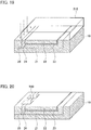
- an electric field relaxation electrode 70 is disposed above the side surfaces of the column regions 22, which face the second main electrode 40. That is, the electric field relaxation electrode 70 is disposed on an upper surface of an interlayer insulating film 80 disposed on an upper surface of the semiconductor layer 20, and the electric field relaxation electrode 70 electrically connects to the second main electrode 40 through an opening portion provided in the interlayer insulating film 80.
- a conductor film such as a metal film is used for the electric field relaxation electrode 70.
- the electric field relaxation electrode 70 and the second main electrode 40 may be formed integrally with each other, for example, by using the same material as the second main electrode 40.
- an insulating film such as a silicon oxide film is used for the interlayer insulating film 80.
- the electric field relaxation electrode 70 is disposed above the boundary region between the drift region 21 and the column regions 22, on which an electric field is likely to concentrate, whereby a gradient of a potential distribution in the boundary region becomes gentle, and the concentration of the electric field can be relaxed. That is, the electric field relaxation electrode 70 is disposed above the boundary region, whereby the depletion layer smoothly extends in the boundary region. A curvature of the depletion layer is controlled as described above, whereby the potential changes gently, and the concentration of the electric field is relaxed. At this time, the electric field relaxation electrode 70 of which potential is the same as that of the second main electrode 40 is disposed above the boundary region close to the second main electrode 40, whereby the concentration of the electric field in the boundary region can be relaxed greatly.
- FIG. 13 illustrates the example where the electric field relaxation electrode 70 is disposed above the side surfaces of the column regions 22, which face the second main electrode 40
- the electric field relaxation electrode 70 may be disposed above side surfaces of the column regions 22, which are adjacent to the drift region 21 in parallel to the current path. That is, the electric field relaxation electrode 70 is disposed above a region on which the electric field concentrates.
- the electric field relaxation electrode 70 may electrically connect to the first main electrode 30 or the control electrodes 50.
- the drift region 21 and the column region 22 are disposed alternately with each other along a thickness direction of the substrate 10, and constitute an SJ structure. Then, the drift region 21, the electric field relaxation region 23 and the column region 22 are laminated on one another in the thickness direction.
- thicknesses thereof are set so as to satisfy Equation (1).
- Other configurations are the same as those of the first embodiment illustrated in FIG. 1 .
- the substrate 10 is doped with the n-type impurities by ion implantation using a patterned mask material 211 as a mask, and the drift region 21 is selectively formed.
- the substrate 10 is a non-doped SiC semiconductor. An intensity of energy of the ion implantation is adjusted, whereby the drift region 21 is formed at a position separate from the main surface of the substrate 10 by the sum of the thickness of the column region 22 and the thickness of the electric field relaxation region 23.
- an exposed portion is formed on a front surface of the drift region 21 by ion implantation using a mask material 212 as a mask.
- a mask material 212 as a mask.
- the substrate 10 is doped with the p-type impurities by ion implantation using mask materials 213 as masks, and the column region 22 is selectively formed.
- an intensity of energy of the ion implantation is adjusted, whereby the electric field relaxation region 23 that is not doped with impurities is formed between the drift region 21 and the column region 22.
- the well region 24 is formed by ion implantation of doping the substrate 10 with the p-type impurities by using mask materials 214 as masks.
- the source region 25 is formed by ion implantation of doping the substrate 10 with the n-type impurities by using a mask material 215 as a mask.
- the gate trenches 500 are formed by dry etching using a patterned mask material (not shown) as a mask. To a depth reaching the substrate 10, the gate trenches 500 are formed at positions in contact with the source region 25, the well region 24, the drift region 21 and the column regions 22.
- the gate trenches 500 are embedded to form the control electrodes 50.
- a method for forming the gate insulating films 60 and the control electrodes 50 is the same as the method described in the first embodiment.
- the semiconductor device illustrated in FIG. 14 is completed.
- the widths of the drift region 21 and the column regions 22 in the horizontal direction parallel to the main surface of the substrate 10 depend on accuracy of the photolithography technology or the like, and for example, are about 1 ⁇ m to several ten micrometers.
- the thicknesses of the drift region 21 and the column regions 22 can be accurately controlled by adjusting the intensities of the energy of the ion implantation of impurity doping. Therefore, the thickness of the drift region 21 and the thickness of the column region 22 can be thinned more than the widths thereof in the horizontal direction, for example, can be set to about several ten nanometers to several hundred nanometers. Hence, a repetition period of the drift region 21 and the column region 22, which constitute the SJ structure, can be shortened. Therefore, in the semiconductor device illustrated in FIG. 14 , it is easy to establish the pinch-off state.
- the drift region 21 and the column region 22 are each a single layer; however, a plurality of the drift regions 21 and a plurality of the column regions 22 may be laminated alternately on each other.
- an SJ structure is configured, in which a plurality of pn junctions are arrayed in a fixed period in the thickness direction of the substrate 10. With this configuration, the withstand voltage of the semiconductor device can be further enhanced.
- the semiconductor device according to the second embodiment of the present invention a decrease of the withstand voltage of the semiconductor device can be reduced, the semiconductor device having the SJ structure in which the drift regions 21 and the column regions 22 are arranged alternately with each other along the thickness direction of the substrate 10. Others are substantially similar to those of the first embodiment, and a duplicate description will be omitted.
- such semiconductor layers 20 are formed on side surfaces of a groove 100 formed on the main surface of the substrate 10.
- a thickness in a surface normal direction of the side surfaces of the groove (hereinafter, this direction will be referred to as a "surface normal direction") is set so as to satisfy Equation (1).
- SJ structures are configured on the side surfaces of the groove of the substrate 10 along the surface normal direction.
- the electric field relaxation regions 23 are disposed in contact with the side surfaces of the column regions 22, which face the second main electrodes 40. Moreover, the electric field relaxation regions 23 disposed in contact with the side surfaces of the column regions 22 which face the drift regions 21 in parallel to the current path are disposed between the drift regions 21 and the column regions 22 along the surface normal direction. Therefore, the decrease of the withstand voltage of the semiconductor device can be reduced.
- the drift regions 21 and the column regions 22 are formed on the side surfaces of the groove 100, whereby the width of the current path can be widened in a depth direction of the substrate 10. Therefore, the on-resistance per substrate area decreases.
- the semiconductor layers 20 are formed by ion-implanting the impurities from obliquely above to the groove 100 formed on the main surface of the substrate 10 by etching.
- a semiconductor device has a diode structure in which the well region 24 connects to the first main electrode 30. That is, the semiconductor device illustrated in FIG. 23 operates as a pn junction diode in which the first main electrode 30 is anode electrode and the second main electrode 40 is a cathode electrode. Also in the semiconductor device illustrated in FIG. 23 , the drift region 21 and the column regions 22 are arranged alternately with each other along the direction perpendicular to the current path, whereby an SJ structure is configured. End portions of the drift region 21 and the column regions 22 connect to the well region 24, and other end portion of the drift region 21 connects to the second main electrode 40.
- a low voltage forward voltage
- a high voltage reverse voltage
- the concentration of the electric field is relaxed by the electric field relaxation regions 23 disposed between the drift region 21 and the column regions 22, and the withstand voltage improves. Note that a leakage current at an off-time can be suppressed in the pn junction diode in which the well region 24 is disposed between the first main electrode 30 and the drift region 21 and the column regions 22.
- the semiconductor device according to the embodiment may be a Schottky barrier diode (SBD) in which the drift region 21 and the first main electrode 30 connect to each other.
- the well region 24 is not disposed between the drift region 21 and the first main electrode 30, and the drift region 21 and the first main electrode 30 electrically connect to each other while having an energy barrier on an interface therebetween.
- the second main electrode 40 makes an ohmic connection to the drift region 21.
- a metal material such as nickel and platinum, which has a high work function, is used for the first main electrode 30, whereby a Schottky junction is formed between the drift region 21 and the first main electrode 30.
- a material such as titanium, which has a low work function and makes an ohmic connection to the drift region 21, is used.
- the electric field relaxation regions 23 are disposed between the drift region 21 and the column regions 22, whereby the concentration of the electric field can be relaxed.
- the semiconductor device may be a transistor with another structure.
- the present invention is also applicable to a bipolar transistor in which the first main electrode 30 is an emitter electrode, the second main electrode 40 is a collector electrode, and the control electrode 50 is a base electrode.
- the semiconductor device of the present invention and the method for manufacturing the semiconductor device are usable for an electronic device industry including manufacturers which manufacture the semiconductor device having the SJ structure.
Landscapes
- Insulated Gate Type Field-Effect Transistor (AREA)
- Electrodes Of Semiconductors (AREA)
- Thin Film Transistor (AREA)
Abstract
Description
- The present invention relates to a semiconductor device and a method for manufacturing the same.
- In order to achieve a high withstand voltage and a low on-resistance, a semiconductor device with a super junction (SJ) structure has been developed (see Patent Literature 1). The SJ structure is a structure in which n-type drift regions and p-type column regions are arranged alternately with each other to periodically form pn junctions. In the semiconductor device with the SJ structure, even if a concentration of N-type impurities in the drift regions through which a main current flows is increased to lower the on-resistance, the withstand voltage thereof can be kept high since the drift regions are depleted at the time of reverse bias by depletion layers which extend from the pn junction.
- [Patent Literature] Japanese Patent Laid-Open Publication No.
2002-319680 - However, there has been a problem that the withstand voltage of the semiconductor device decreases by the fact that an electric field concentrates to boundaries between the drift regions and the column regions at the time of reverse bias.
- The present invention has been made in consideration of the above-described problem, and has an object to provide a semiconductor device that has a super junction structure and is capable of suppressing the decrease of the withstand voltage and to provide a method for manufacturing the semiconductor device.
- A semiconductor device according to an aspect of the present invention includes, in at least a part between a drift region and a column region which constitute a super junction structure, an electric field relaxation region that is either a low-concentration region in which an impurity concentration is lower than in a same conductivity-type adjacent region or a non-doped region.
- A method for manufacturing a semiconductor device according to another aspect of the present invention includes forming a drift region and a column region by ion-implanting impurities into a substrate, wherein an electric field relaxation region that is either a low-concentration region in which an impurity concentration is lower than in a same conductivity-type adjacent region or a non-doped region is formed in at least part between the drift region and the column region.
- According to the present invention, a semiconductor device that has a super junction structure and is capable of suppressing the decrease of the withstand voltage and a method for manufacturing the semiconductor device can be provided.
-
-
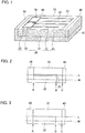
FIG. 1 is a schematic perspective view illustrating a configuration of a semiconductor device according to a first embodiment of the present invention. -
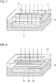
FIG. 2 is a plan view illustrating an example model for calculating an electric field intensity. -
FIG. 3 is a plan view illustrating a comparative example model for calculating the electric field intensity. -
FIG. 4 is a graph illustrating a result of calculating the electric field intensity. -
FIG. 5 is a graph illustrating a result of calculating the electric field intensity. -
FIG. 6 is a graph illustrating a result of calculating the electric field intensity. -
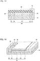
FIG. 7 is a perspective view for explaining a method for manufacturing the semiconductor device according to the first embodiment of the present invention (No. 1). -
FIG. 8 is a perspective view for explaining the method for manufacturing the semiconductor device according to the first embodiment of the present invention (No. 2). -
FIG. 9 is a perspective view for explaining the method for manufacturing the semiconductor device according to the first embodiment of the present invention (No. 3). -
FIG. 10 is a perspective view for explaining the method for manufacturing the semiconductor device according to the first embodiment of the present invention (No. 4). -
FIG. 11 is a perspective view for explaining the method for manufacturing the semiconductor device according to the first embodiment of the present invention (No. 5). -
FIG. 12 is a perspective view for explaining the method for manufacturing the semiconductor device according to the first embodiment of the present invention (No. 6). -
FIG. 13 is a schematic cross-sectional view illustrating a configuration of a semiconductor device according to a modified example of the first embodiment of the present invention. -
FIG. 14 is a schematic perspective view illustrating a configuration of a semiconductor device according to a second embodiment of the present invention. -
FIG. 15 is a perspective view for explaining a method for manufacturing the semiconductor device according to the second embodiment of the present invention (No. 1). -
FIG. 16 is a perspective view for explaining the method for manufacturing the semiconductor device according to the second embodiment of the present invention (No. 2). -
FIG. 17 is a perspective view for explaining the method for manufacturing the semiconductor device according to the second embodiment of the present invention (No. 3). -
FIG. 18 is a perspective view for explaining the method for manufacturing the semiconductor device according to the second embodiment of the present invention (No. 4). -
FIG. 19 is a perspective view for explaining the method for manufacturing the semiconductor device according to the second embodiment of the present invention (No. 5). -
FIG. 20 is a perspective view for explaining the method for manufacturing the semiconductor device according to the second embodiment of the present invention (No. 6). -
FIG. 21 is a perspective view for explaining the method for manufacturing the semiconductor device according to the second embodiment of the present invention (No. 7). -
FIG. 22 is a schematic perspective view illustrating a configuration of a semiconductor device according to a third embodiment of the present invention. -
FIG. 23 is a schematic perspective view illustrating a configuration of a semiconductor device according to a fourth embodiment of the present invention. -
FIG. 24 is a schematic perspective view illustrating another configuration of the semiconductor device according to the fourth embodiment of the present invention. - Hereinafter, a description will be given of embodiments with reference to the drawings. In the description of the drawings, the same reference numerals are assigned to the same portions, and a description thereof is omitted. However, the drawings are schematic, and relationships between thicknesses and plane dimensions, ratios of thicknesses of the respective layers, and the like include portions different from actual ones. Moreover, between the drawings, portions where dimensional relationships and ratios therebetween are different from each other are also included.
- As illustrated in
FIG. 1 , a semiconductor device according to a first embodiment of the present invention includes: asubstrate 10; asemiconductor layer 20 disposed on a main surface of thesubstrate 10; and a firstmain electrode 30 and a secondmain electrode 40, which are disposed on thesubstrate 10 separately from each other with thesemiconductor layer 20 sandwiched therebetween. The firstmain electrode 30 and the secondmain electrode 40 are individually end portions of a current path of a main current flowing through the semiconductor device in an on-state. - The
semiconductor layer 20 includes: a first conductivity-type drift region 21 through which the main current flows; and second conductivity-type column regions 22 and electricfield relaxation regions 23, which are disposed inside thedrift region 21. Each of the electricfield relaxation regions 23 is disposed in at least a part between thedrift region 21 and thecolumn region 22. Thecolumn regions 22 extend in parallel to the current path. An SJ structure is composed of thedrift regions 21 and thecolumn regions 22. The electricfield relaxation regions 23 are low-concentration regions in which an impurity concentration is lower than in adjacent regions with the same conductivity type, or non-doped regions which are not intentionally doped with impurities. In the semiconductor device illustrated inFIG. 1 , the electricfield relaxation regions 23 are disposed in contact with side surfaces of thecolumn regions 22, which face the secondmain electrode 40, and are disposed in contact with side surfaces of thecolumn regions 22 facing thedrift region 21 in parallel to the current path. - The first conductivity type and the second conductivity type are conductivity types opposite to each other. That is, if the first conductivity type is the n type, then the second conductivity type is the p-type, and the first conductivity type is the p-type, then the second conductivity type is the n-type. Hereinafter, a description will be given of the case where the first second conductivity type is the n-type and the second conductivity type is the p-type.
- The
semiconductor layer 20 illustrated inFIG. 1 further includes: a second conductivity-type well region 24 disposed between the firstmain electrode 30 and respective end portions of thedrift region 21 and thecolumn regions 22; and a first conductivity-type source region 25 disposed between thewell region 24 and the firstmain electrode 30. Thewell region 24 contacts thedrift region 21 and thecolumn regions 22. Thesource region 25 electrically connects to the firstmain electrode 30. - Moreover, the semiconductor device illustrated in
FIG. 1 further includescontrol electrodes 50 embedded in thesemiconductor layer 20. Thecontrol electrodes 50 face thedrift region 21, thewell region 24 and thesource region 25 withgate insulating films 60 interposed therebetween. The semiconductor device according to the first embodiment operates as a transistor that controls the main current by thecontrol electrodes 50. That is, the semiconductor device illustrated inFIG. 1 is a MOSFET in which the firstmain electrode 30 is a source electrode, the secondmain electrode 40 is a drain electrode, and thecontrol electrodes 50 are gate electrodes. The firstmain electrode 30 makes an ohmic connection to thesource region 25. The secondmain electrode 40 makes an ohmic connection to thedrift region 21. - A plurality of gate trenches are formed so as to reach the
substrate 10. Opening portions of the gate trenches lie astride upper surfaces of thesource region 25, thecolumn regions 22 and thewell region 24. Thegate insulating films 60 are disposed on inner wall surfaces of the gate trenches, and thecontrol electrodes 50 are disposed inside the gate trenches so that a periphery thereof is surrounded by thegate insulating films 60. Between the gate trenches, thedrift region 21 and thewell region 24 connect to each other, and thewell region 24 and thesource region 25 connect to each other. At the time of an on-operation, an inversion layer is formed in a channel region of thewell region 24, which contacts thegate insulating films 60. - The semiconductor device illustrated in
FIG. 1 has such an SJ structure in which a plurality of thedrift regions 21 and a plurality of thecolumn regions 22 are arranged alternately with each other along a direction perpendicular to the current path. Therefore, at the time of reverse voltage application (at the time of reverse bias), thedrift region 21 and thecolumn regions 22 are depleted by depletion layers which extend from pn junctions formed on interfaces between thedrift region 21 and thecolumn regions 22. Therefore, a high withstand voltage is obtained for the semiconductor device. - Further, in the semiconductor device illustrated in
FIG. 1 , the electricfield relaxation regions 23 are disposed between thedrift region 21 and thecolumn region 22. When the electricfield relaxation regions 23 are not non-doped regions, the electricfield relaxation regions 23 are of the same conductivity type as that of either of thedrift region 21 and thecolumn regions 22, which are adjacent thereto; however, the impurity concentration of the electricfield relaxation regions 23 is lower than an impurity concentration of the regions of the same conductivity type. That is, when the electricfield relaxation regions 23 are of the first conductivity type, the impurity concentration of the electricfield relaxation regions 23 is lower than the impurity concentration of thedrift region 21. Meanwhile, when the electricfield relaxation regions 23 are of the second conductivity type, the impurity concentration of the electricfield relaxation regions 23 is lower than the impurity concentration of thecolumn regions 22. Therefore, by the electricfield relaxation regions 23, electric field concentration in boundary regions where thedrift region 21 and thecolumn regions 22 face each other is relaxed. A width of the electricfield relaxation regions 23 is, for example, approximately 0.1 µm to 0.3 µm. - Note that, when the
drift region 21 is of the n-type, and the electricfield relaxation regions 23 is of the p-type, then the impurity concentration of the electricfield relaxation regions 23 may be higher than that of thedrift region 21. Moreover, when thecolumn regions 22 are of the p-type, and the electricfield relaxation regions 23 are of the n-type, then the impurity concentration of the electricfield relaxation regions 23 may be higher than thecolumn regions 22. - Hereinafter, a description will be given of basic operations of the semiconductor device illustrated in
FIG. 1 . - In an on-operation, a potential of the
control electrodes 50 is controlled in a state in which a positive potential is applied to the secondmain electrode 40 while taking a potential of the firstmain electrode 30 as a reference, whereby the semiconductor device operates as a transistor. That is, a voltage between thecontrol electrodes 50 and the firstmain electrode 30 is set to a predetermined threshold voltage or more, whereby inversion layers are formed in channel regions of thewell region 24 on side surfaces of thecontrol electrodes 50. Thus, the semiconductor device turns to an on-state, and the main current flows between the firstmain electrode 30 and the secondmain electrode 40. - Meanwhile, in an off-operation, the voltage between the
control electrodes 50 and the firstmain electrode 30 is set equal to or less than the predetermined threshold voltage. Thus, the inversion layer disappears, and the main current is shielded. - In an off-state, the depletion layers spread from the interfaces between the
drift region 21 and thecolumn regions 22, and when the reverse voltage increase to some extent, thedrift region 21 and thecolumn regions 22 turn to a pinch-off state. Thus, an electric field intensity of thedrift region 21 and thecolumn regions 22 forms a uniform rectangular distribution, and a maximum electric field applied to the semiconductor device decreases greatly. Thus, the withstand voltage of the semiconductor device improves. - In order to obtain a high withstand voltage by completely depleting the SJ structure in the off-state, it is required to set, to approximately 1, a ratio of a total amount of n-type impurities of the n-type semiconductor region and a total amount of p-type impurities of the p-type semiconductor regions. Therefore, the concentration Nd of the n-type impurities of the
drift region 21, the concentration Na of the p-type impurities of thecolumn regions 22, a width Wn of thedrift region 21, and a width Wp of thecolumn regions 22 are set so as to satisfy the following Equation (1).
drift region 21 and thecolumn regions 22 are arranged alternately with each other. - The impurity concentrations of the
drift region 21 and thecolumn regions 22 are set so as to satisfy Equation (1), whereby thedrift region 21 and thecolumn regions 22 are depleted by the depletion layers which extend from the pn junctions. Therefore, the withstand voltage of the semiconductor device is high. In addition, a resistance value of thedrift region 21 can be reduced. - However, at the time of reverse bias, the electric field is likely to concentrate on the pn junctions in the interfaces between the
drift region 21 and thecolumn regions 22. This is because the relationship of Equation (1) is not established in regions close to the pn junctions, and electric charges in the n-type semiconductor region and the p-type semiconductor regions are not balanced. The withstand voltage of the semiconductor device decreases when the electric field concentrates on the pn junctions. - In contrast, in the semiconductor device illustrated in
FIG. 1 , the electricfield relaxation regions 23 are arranged between thedrift region 21 and thecolumn regions 22, whereby the electric field concentration is relaxed. An effect of relaxing the electric field concentration by the electricfield relaxation regions 23 will be described below by using models individually illustrated inFIG. 2 and FIG. 3 . - The model illustrated in
FIG. 2 is an example model in which the electricfield relaxation region 23 is disposed between thedrift region 21 and thecolumn region 22 as in the semiconductor device illustrated inFIG. 1 . Meanwhile, the model illustrated inFIG. 3 is a comparative example model in which the electricfield relaxation region 23 is not disposed between thedrift region 21 and thecolumn region 22. Note that the electricfield relaxation region 23 is a non-doped region. -
FIG. 4 and FIG. 5 illustrate calculation results of electric field intensities along centerlines M which pass through around the crosswise centers of thecolumn regions 22 in the example model illustrated inFIG. 2 and the comparative example model illustrated inFIG. 3 . InFIG. 4 and FIG. 5 , the electric field intensity of the example model is illustrated by a characteristic E1 as a solid line, and the electric field intensity of the comparative example model is illustrated by a characteristic E2 as a broken line. A position A is a position where thewell region 24 and thecolumn region 22 connect to each other, a position B is a position of a side surface of thecolumn region 22, which faces the secondmain electrode 40, and a position C is a position where thedrift region 21 and the secondmain electrode 40 connect to each other. -
FIG. 4 illustrates calculation results of electric field intensities on front surfaces of the semiconductor layers 20. As illustrated inFIG. 4 , the electric field intensity of the example model is lower than of the comparative example model at the position B where the electric field intensity has a peak value. That is, in comparison with the comparative example model, an electric field distribution is more uniform in the example model. As described above, the concentration of the electric field on the side surface of thecolumn region 22, which faces the secondmain electrode 40, is relaxed by the electricfield relaxation region 23. -
FIG. 5 illustrates calculation results of electric field intensity distributions at plane levels equivalent to bottom surfaces of the secondmain electrodes 40. As illustrated inFIG. 5 , the electric field intensities have peak values also at the position C where thedrift region 21 and the secondmain electrode 40 connect to each other. In the example model, the electric field intensity is lower than in the comparative example model from the position B to the position C, and the concentration of the electric field is relaxed by the electricfield relaxation region 23. - As illustrated in
FIG. 5 , the electric field concentrates on a corner portion of the secondmain electrode 40 in the inside of thesemiconductor layer 20. Therefore, when the electricfield relaxation region 23 is formed to a depth of the bottom surface of thesemiconductor layer 20, the electric field is diffused along a depth direction, and the concentration of the electric field can be relaxed. Hence, the electricfield relaxation region 23 may be formed so as to reach the main surface of thesubstrate 10. - As described above, the electric field is concentrated on the region between each
column region 22 and the secondmain electrode 40. Therefore, though the electricfield relaxation region 23 is disposed on the entire region of the boundary between thedrift region 21 and thecolumn region 22 in the semiconductor device illustrated inFIG. 1 , the electricfield relaxation region 23 may be disposed in contact with only the side surface of thecolumn region 22, which faces the secondmain electrode 40. The electricfield relaxation region 23 is not disposed on side surfaces of thecolumn region 22, which face thedrift region 21 in parallel to the current path, whereby the width of thedrift region 21 is not narrowed, and an increase of an electrical resistance in the current path of the main current can be suppressed. - However, the concentration of the electric field also occurs in the boundary region where the
drift region 21 and thecolumn region 22 face each other, the boundary region being parallel to the current path.FIG. 6 illustrates electric field intensity distributions along boundary lines L illustrated inFIG. 2 and FIG. 3 . As illustrated inFIG. 6 , an electric field intensity distribution of the example model is more uniform in comparison with the comparative example model in which the electric field intensity has a peak value at the position B. As described above, the concentration of the electric field is relaxed by the electricfield relaxation region 23 also in the boundary region between thedrift region 21 and thecolumn region 22, the boundary region being parallel to the current path. Therefore, as illustrated inFIG. 1 , each electricfield relaxation region 23 may be disposed on the side surface of thecolumn region 22, which faces thedrift region 21 in parallel to the current path. - As described above, in accordance with the semiconductor device according to the first embodiment of the present invention, the electric
field relaxation region 23 is disposed on at least a part between thedrift region 21 and thecolumn region 22, whereby the concentration of the electric field is relaxed. As a result, the decrease of the withstand voltage of the semiconductor device having the SJ structure can be decreased. - For the
substrate 10, a semi-insulating substrate and an insulating substrate are suitably used. Thus, an element separation process at the time of integrating a plurality of semiconductor devices on thesame substrate 10 can be simplified. Moreover, at the time of mounting the semiconductor device on a cooler, it is possible to omit an insulating substrate placed between thesubstrate 10 and the cooler. Here, the insulating substrate refers to a substrate with resistivity of several kΩ·cm or more. - For example, a silicon carbide (SiC) substrate having insulating properties is used for the
substrate 10. SiC has some polytypes (crystal polymorphisms), and an SiC substrate with typical 4H can be used for thesubstrate 10. The SiC substrate is used for thesubstrate 10, whereby the insulating properties of thesubstrate 10 can be increased, and thermal conductivity thereof can be increased. Therefore, the back surface of thesubstrate 10 can be directly attached to a cooling mechanism, and the semiconductor device can be cooled efficiently. In accordance with this structure, since thermal conductivity of the SiC substrate is large, heat generated by the main current can be radiated efficiently when the semiconductor device is in the on-state. Moreover, SiC is a wide band gap semiconductor in which the number of intrinsic carriers is small, and accordingly, easily achieves high insulating properties. Therefore, use of the SiC substrate makes it possible to achieve a semiconductor device with a high withstand voltage. - Hereinafter, a method for manufacturing the semiconductor device according to the first embodiment of the present invention will be described with reference to the drawings. Note that the method for manufacturing a semiconductor device, which will be mentioned below, is merely an example, and the semiconductor device is achievable by a variety of manufacturing methods other than this mentioned method, the manufacturing methods including modified examples thereof. Hereinafter, a description will be given of the case of using a non-doped SiC substrate for the
substrate 10. - First, as illustrated in
FIG. 7 , thesubstrate 10 is doped with the n-type impurities by ion implantation using a patternedmask material 111 as a mask, and thedrift region 21 is selectively formed. In order to make the structure easy to understand, only an outer edge of the mask material is illustrated (the same applies below). - As a general mask material, a silicon oxide film can be used, and as a deposition method, a thermal CVD method or a plasma CVD method can be used. As a patterning method, a photolithography method can be used. That is, the mask material is etched by using a patterned photoresist film_as a mask. As an etching method, wet etching using hydrofluoric acid and dry etching such as reactive ion etching can be used. Thereafter, the photoresist film is removed by oxygen plasma, sulfuric acid or the like. In this way, the mask material is patterned.
- Next, the
column regions 22 which extend in parallel to thedrift region 21 are formed inside thedrift region 21 so as to form the electricfield relaxation regions 23 in at least a part between thedrift region 21 and thecolumn regions 22 themselves. That is, as illustrated inFIG. 8 , thesubstrate 10 is doped with the p-type impurities by ion implantation using a patternednew mask material 112 as a mask, and thecolumn regions 22 are selectively formed. Themask material 112 is designed so that, at this time, an exposed region of thesubstrate 10 is narrower than a region thereof in which thedrift region 21 is not formed. Thus, the non-doped electricfield relaxation regions 23 are formed between thedrift region 21 and thecolumn regions 22. - Thereafter, as illustrated in
FIG. 9 , thewell region 24 is formed by ion implantation of doping thesubstrate 10 with the p-type impurities by using amask material 113 as a mask. Moreover, as illustrated inFIG. 10 , thesource region 25 is formed by ion implantation of doping thesubstrate 10 with the n-type impurities by using amask material 114 as a mask. - In the ion implantation, for example, nitrogen (N) is used as the n-type impurities, and aluminum and boron are used as the p-type impurities. Note that a crystal defect can be suppressed from occurring in ion-implanted regions by performing the ion implantation in a state of heating the
substrate 10 to a temperature of approximately 600°C. Then, the ion-implanted impurities are activated by being subjected to heat treatment. For example, heat treatment at approximately 1700°C is performed in an argon atmosphere or a nitrogen atmosphere. - The impurity concentrations of the
column regions 22 and thedrift region 21 are, for example, approximately 1E15/cm3 to 1E19/cm3. However, the impurity concentrations of thedrift region 21 and thecolumn regions 22 are set so as to satisfy the relationship of Equation (1) so that thedrift region 21 and thecolumn regions 22 are depleted by the depletion layers generated between thedrift region 21 and thecolumn regions 22 in an off-state. - An impurity concentration of the
well region 24 is, for example, approximately 1E15/cm3 to 1E19/cm3. Moreover, an impurity concentration of thesource region 25 is, for example, approximately 1E18/cm3 to 1E21/cm3. - Note that manufacturing cost can be reduced in the case of ion-implanting impurities into the
substrate 10 to form thedrift region 21 and thecolumn regions 22 more than in the case forming thedrift region 21 and thecolumn regions 22 by epitaxial growth. - Next, as illustrated in
FIG. 11 ,gate trenches 500 are formed by dry etching using a patterned mask material (not shown) as a mask. To a depth reaching thesubstrate 10, thegate trenches 500 are formed at positions in contact with thesource region 25, thewell region 24, thedrift region 21 and thecolumn regions 22. - Thereafter, the
gate insulating films 60 are formed on inner wall surfaces of thegate trenches 500. A method for forming thegate insulating films 60 may by either a thermal oxidation method or a deposition method. As an example, in the case of the thermal oxidation method, the substrate is heated to a temperature of approximately 1100°C in an oxygen atmosphere. Thus, a silicon oxide film is formed on all portions where the substrate contacts oxygen. - After the
gate insulating films 60 are formed, annealing treatment at approximately 1000°C may be performed in an atmosphere of nitrogen, argon, N2O or the like in order to reduce an interface state on interfaces between thewell region 24 and thegate insulating films 60. Moreover, thermal oxidation in an atmosphere of rigid NO or N2O is also possible. A temperature in that case is suitably 1100°C to 1400°C. A thickness of thegate insulating films 60 is about several ten nanometers. - Next, the
gate trenches 500 are embedded to form thecontrol electrodes 50. A general material of thecontrol electrodes 50 is polysilicon films, and a description will be given here of the case of using the polysilicon films for thecontrol electrodes 50. - A reduced pressure CVD method or the like can be used as the deposition method of the polysilicon films. For example, a thickness of the polysilicon films to be deposited is set to a value larger than a half of a width of each of the
gate trenches 500, and thegate trenches 500 are embedded with the polysilicon films. Since the polysilicon films are formed from the inner wall surfaces of thegate trenches 500, thegate trenches 500 can be completely embedded with the polysilicon films by setting the thickness of the polysilicon films as described above. For example, when the width of thegate trenches 500 is 2 µm, the polysilicon films are formed so that a film thickness thereof becomes thicker than 1 µm. Moreover, after the polysilicon films are deposited, annealing treatment at 950°C is performed in phosphorus oxychloride (POCl3), whereby n-type polysilicon films are formed to impart conductivity to thecontrol electrodes 50. - Next, as illustrated in
FIG. 12 , the polysilicon films are etched to be planarized. A method of the etching may be isotropic etching or anisotropic selective etching. An amount of the etching is set so that the polysilicon films remain inside thegate trenches 500. For example, when the polysilicon films are deposited to a thickness of 1.5 µm for thegate trenches 500 with a width of 2 µm, the amount of etching the polysilicon films is set to 1.5 µm. However, in control for the etching, no problem occurs in the case of over etching of several percent with respect to the amount of etching of 1.5 µm. - Thereafter, the first
main electrode 30 and the secondmain electrode 40, which face each other with thesemiconductor layer 20 sandwiched therebetween, are formed separately from each other on thesubstrate 10 along a direction where thedrift region 21 extends. For example, the firstmain electrode 30 and the secondmain electrode 40 are formed on predetermined regions formed by selectively etching thesubstrate 10 by using an etching mask patterned by a photolithography technology and the like. Thus, the semiconductor device illustrated inFIG. 1 is completed. - As a material of the first
main electrode 30 and the secondmain electrode 40, there can be used metal materials such as titanium (Ti), nickel (Ni) and molybdenum (Mo) and laminated films of Ti/Ni/Ag and the like. For example, after such a metal material is entirely deposited by a sputtering method, an EB evaporation method or the like, the metal material is etched by dry etching using a patterned photoresist film as a mask, and each of the firstmain electrode 30 and the secondmain electrode 40 is formed. Alternatively, the firstmain electrode 30 and the secondmain electrode 40 may be formed by a plating process. - In accordance with the method for manufacturing a semiconductor device, which is described above, the electric
field relaxation regions 23 are formed between thedrift region 21 and thecolumn regions 22. Therefore, the concentration of the electric field at the time of reverse bias is relaxed, and the decrease of the withstand voltage of the semiconductor device having the SJ structure can be suppressed. - Note that, in the above, the description is given of the case of forming the electric
field relaxation regions 23 as non-doped semiconductor regions by leaving a part of thenon-doped substrate 10 between thedrift region 21 and thecolumn regions 22. However, the electricfield relaxation regions 23 are not limited to the non-doped regions. That is, the electricfield relaxation regions 23 may be either n-type semiconductor regions formed by doping thesubstrate 10 with n-type impurities or p-type semiconductor regions formed by doping thesubstrate 10 with p-type impurities. - For example, when the
drift region 21 is an n-type semiconductor region, and thecolumn regions 22 are p-type semiconductor regions, then the electricfield relaxation regions 23 may be set to be n-type semiconductor regions having a lower impurity concentration than thedrift region 21. Alternatively, the electricfield relaxation regions 23 may be set to be p-type semiconductor regions having a lower impurity concentration than thecolumn regions 22. - In the above, the description is given of the example of using an SiC substrate for the
substrate 10; however, a semi-insulating substrate or an insulating substrate other than the SiC substrate may be used for thesubstrate 10. For example, a GaN substrate, a diamond substrate, a zinc oxide (ZnO) substrate, an AlGaN substrate and the like, which are wide band gap substrates, may be used for thesubstrate 10. - Moreover, a wide band gap semiconductor may be used for the
semiconductor layer 20. Thus, it is possible to increase the impurity concentration while keeping on maintaining the withstand voltage to be high. Therefore, the withstand voltage of the semiconductor device can be increased, and the on-resistance can be reduced. - Further, the
semiconductor layer 20 in which the respective regions are made of the same material is used, whereby active regions of the semiconductor device are formed of the same semiconductor material. Thus, a malfunction caused by an occurrence of a defect due to junction of different types of semiconductor materials can be eliminated, and reliability of the semiconductor device can be improved. - Note that, in the above, the description is given of the example of using the first conductivity-type polysilicon films for the
control electrodes 50; however, second conductivity-type polysilicon films may be used for thecontrol electrodes 50. Moreover, other semiconductor materials may be used for thecontrol electrodes 50, or other conductive materials such as metal materials may be used. For example, second conductivity-type poly silicon carbide, SiGe, Al and the like can be used for the materials of thecontrol electrodes 50. - Further, though the example of using the silicon oxide films for the
gate insulating films 60 is described, silicon nitride films may be used for thegate insulating films 60. Moreover, laminated films of the silicon oxide films and the silicon nitride films may be used for thegate insulating films 60. Isotropic etching in the case of using the silicon nitride films for thegate insulating films 60 can be performed by washing using hot phosphoric acid at 160°C. - A semiconductor device according to a modified example of the first embodiment of the present invention further includes an electric field relaxation electrode disposed so as to cover at least a part of the region where the
drift region 21 and thecolumn regions 22 face each other. In the semiconductor device according to the modified example, which is illustrated inFIG. 13 , an electricfield relaxation electrode 70 is disposed above the side surfaces of thecolumn regions 22, which face the secondmain electrode 40. That is, the electricfield relaxation electrode 70 is disposed on an upper surface of aninterlayer insulating film 80 disposed on an upper surface of thesemiconductor layer 20, and the electricfield relaxation electrode 70 electrically connects to the secondmain electrode 40 through an opening portion provided in theinterlayer insulating film 80. - A conductor film such as a metal film is used for the electric
field relaxation electrode 70. The electricfield relaxation electrode 70 and the secondmain electrode 40 may be formed integrally with each other, for example, by using the same material as the secondmain electrode 40. For example, an insulating film such as a silicon oxide film is used for theinterlayer insulating film 80. - In the semiconductor device illustrated in
FIG. 13 , the electricfield relaxation electrode 70 is disposed above the boundary region between thedrift region 21 and thecolumn regions 22, on which an electric field is likely to concentrate, whereby a gradient of a potential distribution in the boundary region becomes gentle, and the concentration of the electric field can be relaxed. That is, the electricfield relaxation electrode 70 is disposed above the boundary region, whereby the depletion layer smoothly extends in the boundary region. A curvature of the depletion layer is controlled as described above, whereby the potential changes gently, and the concentration of the electric field is relaxed. At this time, the electricfield relaxation electrode 70 of which potential is the same as that of the secondmain electrode 40 is disposed above the boundary region close to the secondmain electrode 40, whereby the concentration of the electric field in the boundary region can be relaxed greatly. - Note that, though
FIG. 13 illustrates the example where the electricfield relaxation electrode 70 is disposed above the side surfaces of thecolumn regions 22, which face the secondmain electrode 40, the electricfield relaxation electrode 70 may be disposed above side surfaces of thecolumn regions 22, which are adjacent to thedrift region 21 in parallel to the current path. That is, the electricfield relaxation electrode 70 is disposed above a region on which the electric field concentrates. Moreover, though the example where the electricfield relaxation electrode 70 electrically connects to the secondmain electrode 40, the electricfield relaxation electrode 70 may electrically connect to the firstmain electrode 30 or thecontrol electrodes 50. - In a semiconductor device according to a second embodiment of the present invention, as illustrated in
FIG. 14 , thedrift region 21 and thecolumn region 22 are disposed alternately with each other along a thickness direction of thesubstrate 10, and constitute an SJ structure. Then, thedrift region 21, the electricfield relaxation region 23 and thecolumn region 22 are laminated on one another in the thickness direction. In the semiconductor device illustrated inFIG. 14 , in place of the impurity concentrations and widths of thedrift region 21 and thecolumn regions 22, thicknesses thereof are set so as to satisfy Equation (1). Other configurations are the same as those of the first embodiment illustrated inFIG. 1 . - Hereinafter, a method for manufacturing the semiconductor device according to the second embodiment of the present invention will be described with reference to the drawings. Note that the method for manufacturing a semiconductor device, which will be mentioned below, is merely an example, and the semiconductor device is achievable by a variety of manufacturing methods other than this mentioned method, the manufacturing methods including modified examples thereof.
- First, as illustrated in
FIG. 15 , thesubstrate 10 is doped with the n-type impurities by ion implantation using a patternedmask material 211 as a mask, and thedrift region 21 is selectively formed. Thesubstrate 10 is a non-doped SiC semiconductor. An intensity of energy of the ion implantation is adjusted, whereby thedrift region 21 is formed at a position separate from the main surface of thesubstrate 10 by the sum of the thickness of thecolumn region 22 and the thickness of the electricfield relaxation region 23. - Subsequently, as illustrated in
FIG. 16 , an exposed portion is formed on a front surface of thedrift region 21 by ion implantation using amask material 212 as a mask. For example, thedrift region 21 of a portion on which thecolumn region 22 is not laminated, the portion connecting to the secondmain electrode 40, is formed. - Next, as illustrated in
FIG. 17 , thesubstrate 10 is doped with the p-type impurities by ion implantation usingmask materials 213 as masks, and thecolumn region 22 is selectively formed. At this time, an intensity of energy of the ion implantation is adjusted, whereby the electricfield relaxation region 23 that is not doped with impurities is formed between thedrift region 21 and thecolumn region 22. - Thereafter, as illustrated in
FIG. 18 , thewell region 24 is formed by ion implantation of doping thesubstrate 10 with the p-type impurities by usingmask materials 214 as masks. Moreover, as illustrated inFIG. 19 , thesource region 25 is formed by ion implantation of doping thesubstrate 10 with the n-type impurities by using amask material 215 as a mask. - Next, as illustrated in
FIG. 20 , thegate trenches 500 are formed by dry etching using a patterned mask material (not shown) as a mask. To a depth reaching thesubstrate 10, thegate trenches 500 are formed at positions in contact with thesource region 25, thewell region 24, thedrift region 21 and thecolumn regions 22. - After the
gate insulating films 60 are formed on the inner wall surfaces of thegate trenches 500, as illustrated inFIG. 21 , thegate trenches 500 are embedded to form thecontrol electrodes 50. A method for forming thegate insulating films 60 and thecontrol electrodes 50 is the same as the method described in the first embodiment. - Thereafter, the first
main electrode 30 and the secondmain electrode 40, which face each other with thesemiconductor layer 20 sandwiched therebetween, are formed separately from each other on thesubstrate 10. In such a way as described above, the semiconductor device illustrated inFIG. 14 is completed. - In the semiconductor device illustrated in
FIG. 1 , the widths of thedrift region 21 and thecolumn regions 22 in the horizontal direction parallel to the main surface of thesubstrate 10 depend on accuracy of the photolithography technology or the like, and for example, are about 1 µm to several ten micrometers. Meanwhile, in the semiconductor device illustrated inFIG. 14 , the thicknesses of thedrift region 21 and thecolumn regions 22 can be accurately controlled by adjusting the intensities of the energy of the ion implantation of impurity doping. Therefore, the thickness of thedrift region 21 and the thickness of thecolumn region 22 can be thinned more than the widths thereof in the horizontal direction, for example, can be set to about several ten nanometers to several hundred nanometers. Hence, a repetition period of thedrift region 21 and thecolumn region 22, which constitute the SJ structure, can be shortened. Therefore, in the semiconductor device illustrated inFIG. 14 , it is easy to establish the pinch-off state. - In
FIG. 14 , thedrift region 21 and thecolumn region 22 are each a single layer; however, a plurality of thedrift regions 21 and a plurality of thecolumn regions 22 may be laminated alternately on each other. Thus, an SJ structure is configured, in which a plurality of pn junctions are arrayed in a fixed period in the thickness direction of thesubstrate 10. With this configuration, the withstand voltage of the semiconductor device can be further enhanced. - As described above, in accordance with the semiconductor device according to the second embodiment of the present invention, a decrease of the withstand voltage of the semiconductor device can be reduced, the semiconductor device having the SJ structure in which the
drift regions 21 and thecolumn regions 22 are arranged alternately with each other along the thickness direction of thesubstrate 10. Others are substantially similar to those of the first embodiment, and a duplicate description will be omitted. - In a semiconductor device according to a third embodiment of the present invention, as illustrated in
FIG. 22 , such semiconductor layers 20 are formed on side surfaces of agroove 100 formed on the main surface of thesubstrate 10. In the semiconductor device illustrated inFIG. 22 , in place of the impurity concentrations and widths of thedrift region 21 and thecolumn regions 22, a thickness in a surface normal direction of the side surfaces of the groove (hereinafter, this direction will be referred to as a "surface normal direction") is set so as to satisfy Equation (1). Thus, in the semiconductor device illustrated inFIG. 22 , SJ structures are configured on the side surfaces of the groove of thesubstrate 10 along the surface normal direction. - Also in the semiconductor device illustrated in
FIG. 22 , the electricfield relaxation regions 23 are disposed in contact with the side surfaces of thecolumn regions 22, which face the secondmain electrodes 40. Moreover, the electricfield relaxation regions 23 disposed in contact with the side surfaces of thecolumn regions 22 which face thedrift regions 21 in parallel to the current path are disposed between thedrift regions 21 and thecolumn regions 22 along the surface normal direction. Therefore, the decrease of the withstand voltage of the semiconductor device can be reduced. - Moreover, in accordance with the semiconductor device illustrated in
FIG. 22 , thedrift regions 21 and thecolumn regions 22 are formed on the side surfaces of thegroove 100, whereby the width of the current path can be widened in a depth direction of thesubstrate 10. Therefore, the on-resistance per substrate area decreases. The semiconductor layers 20 are formed by ion-implanting the impurities from obliquely above to thegroove 100 formed on the main surface of thesubstrate 10 by etching. - As illustrated in
FIG. 23 , a semiconductor device according to a fourth embodiment of the present invention has a diode structure in which thewell region 24 connects to the firstmain electrode 30. That is, the semiconductor device illustrated inFIG. 23 operates as a pn junction diode in which the firstmain electrode 30 is anode electrode and the secondmain electrode 40 is a cathode electrode. Also in the semiconductor device illustrated inFIG. 23 , thedrift region 21 and thecolumn regions 22 are arranged alternately with each other along the direction perpendicular to the current path, whereby an SJ structure is configured. End portions of thedrift region 21 and thecolumn regions 22 connect to thewell region 24, and other end portion of thedrift region 21 connects to the secondmain electrode 40. - In an on-operation, a low voltage (forward voltage) is applied to the second
main electrode 40 while the firstmain electrode 30 is being set to a reference potential, whereby an energy barrier between thewell region 24 and thedrift region 21 lowers. Therefore, electrons come to flow from thedrift region 21 to thewell region 24, and a forward current flows between the firstmain electrode 30 and the secondmain electrode 40. In an off-operation, a high voltage (reverse voltage) is applied to the secondmain electrode 40 while the firstmain electrode 30 is being set to the reference potential, whereby the energy barrier between thewell region 24 and thedrift region 21 rises. Therefore, the electrons come not to flow from thedrift region 21 to thewell region 24. - Also in the semiconductor device having such a diode structure illustrated in
FIG. 23 , the concentration of the electric field is relaxed by the electricfield relaxation regions 23 disposed between thedrift region 21 and thecolumn regions 22, and the withstand voltage improves. Note that a leakage current at an off-time can be suppressed in the pn junction diode in which thewell region 24 is disposed between the firstmain electrode 30 and thedrift region 21 and thecolumn regions 22. - Moreover, as illustrated in
FIG. 24 , the semiconductor device according to the embodiment may be a Schottky barrier diode (SBD) in which thedrift region 21 and the firstmain electrode 30 connect to each other. In the semiconductor device illustrated inFIG. 24 , thewell region 24 is not disposed between thedrift region 21 and the firstmain electrode 30, and thedrift region 21 and the firstmain electrode 30 electrically connect to each other while having an energy barrier on an interface therebetween. Meanwhile, the secondmain electrode 40 makes an ohmic connection to thedrift region 21. - In the semiconductor device illustrated in
FIG. 24 , a metal material such as nickel and platinum, which has a high work function, is used for the firstmain electrode 30, whereby a Schottky junction is formed between thedrift region 21 and the firstmain electrode 30. For the secondmain electrode 40, a material such as titanium, which has a low work function and makes an ohmic connection to thedrift region 21, is used. Also in the SBD illustrated inFIG. 24 , the electricfield relaxation regions 23 are disposed between thedrift region 21 and thecolumn regions 22, whereby the concentration of the electric field can be relaxed. - As above, the present invention has been described by the embodiments; however, it should not be understood that the description and the drawings, which form a part of this disclosure, limit the present invention. For those skilled in the art, varieties of alternative embodiments, examples and application technologies will be obvious from this disclosure.
- For example, in the above, the description is given of the case where the semiconductor device that operates as a transistor is a MOSFET. However, the semiconductor device may be a transistor with another structure. For example, the present invention is also applicable to a bipolar transistor in which the first
main electrode 30 is an emitter electrode, the secondmain electrode 40 is a collector electrode, and thecontrol electrode 50 is a base electrode. - As described above, it is natural that the present invention incorporates a variety of embodiments which are not described herein.
- The semiconductor device of the present invention and the method for manufacturing the semiconductor device are usable for an electronic device industry including manufacturers which manufacture the semiconductor device having the SJ structure.
-
- 10
- Substrate
- 20
- Semiconductor layer
- 21
- Drift region
- 22
- Column region
- 23
- Electric field relaxation region
- 24
- Well region
- 25
- Source region
- 30
- First main electrode
- 40
- Second main electrode
- 50
- Control electrode
- 60
- Gate insulating film
- 70
- Electric field relaxation electrode
Claims (15)
- A semiconductor device comprising:a substrate;a semiconductor layer disposed on a main surface of the substrate; anda first main electrode and a second main electrode, which are disposed on the substrate separately from each other with the semiconductor layer sandwiched therebetween and are individually end portions of a current path of a main current flowing in an on-state,wherein the semiconductor layer includes:a first conductivity-type drift region through which the main current flows;a second conductivity-type column region that is disposed inside the drift region and extends in parallel to the current path; andan electric field relaxation region that is disposed in at least a part between the drift region and the column region and is either a low-concentration region in which an impurity concentration is lower than in a same conductivity-type adjacent region or a non-doped region.
- The semiconductor device according to claim 1,
wherein the electric field relaxation region is disposed on a side surface of the column region, the side surface facing the second main electrode. - The semiconductor device according to claim 1 or 2,
wherein the electric field relaxation region is disposed on a side surface of the column region, the side surface facing the drift region in parallel to the current path. - The semiconductor device according to any one of claims 1 to 3,
wherein impurity concentrations of the drift region and the column region are set so that the drift region and the column region are depleted by a depletion layer generated between the drift region and the column region in an off-state in which the main current is cut off. - The semiconductor device according to any one of claims 1 to 4,
wherein the electric field relaxation region reaches the substrate. - The semiconductor device according to any one of claims 1 to 5,
wherein the semiconductor layer includes a second conductivity-type well region disposed between the drift region and the first main electrode and between the column region and the first main electrode. - The semiconductor device according to claim 6,
wherein the semiconductor layer includes a first conductivity-type source region disposed between the well region and the first main electrode and electrically connected to the first main electrode,
wherein the semiconductor device further includes a control electrode embedded in the semiconductor layer while facing the drift region, the well region and the source region with an insulating film interposed therebetween, and
wherein the semiconductor device operates as a transistor that controls the main current by the control electrode. - The semiconductor device according to any one of claims 1 to 7, further comprising an electric field relaxation electrode disposed so as to cover at least a part of a region where the drift region and the column region face each other and electrically connected to the first main electrode or the second main electrode.
- The semiconductor device according to any one of claims 1 to 8,
wherein, on a side surface of a groove formed in the substrate, the drift region and the column region are arranged alternately with each other along a surface normal direction of the side surface of the groove. - The semiconductor device according to any one of claims 1 to 8,
wherein the drift region and the column region are arranged alternately with each other along a thickness direction of the substrate. - The semiconductor device according to any one of claims 1 to 10,
wherein the semiconductor layer is formed of a wide band gap semiconductor. - The semiconductor device according to any one of claims 1 to 11,
wherein the respective regions of the semiconductor layer are formed of a same material. - The semiconductor device according to any one of claims 1 to 12,
wherein the substrate is a semi-insulating substrate or an insulating substrate. - The semiconductor device according to any one of claims 1 to 12,
wherein the substrate is a silicon carbide substrate. - A method for manufacturing a semiconductor device, the method comprising:forming a first conductivity-type drift region on a main surface of a substrate;forming a second conductivity-type column region inside the drift region, the column region extending in parallel to the drift region, so as to form an electric field relaxation region in at least a part between the column region and the drift region, the electric field relaxation region being either a low-concentration region in which an impurity concentration is lower than in a same conductivity-type adjacent region or a non-doped region; andforming a first main electrode and a second main electrode separately from each other on the substrate along a direction where the drift region extends, the first main electrode and the second main electrode facing each other with the drift region and the column region interposed therebetween,wherein the drift region and the column region are formed by ion-implanting impurities into the substrate.
Applications Claiming Priority (1)
| Application Number | Priority Date | Filing Date | Title |
|---|---|---|---|
| PCT/IB2018/001002 WO2020021298A1 (en) | 2018-07-27 | 2018-07-27 | Semiconductor device and manufacturing method therefor |
Publications (2)
| Publication Number | Publication Date |
|---|---|
| EP3832698A1 true EP3832698A1 (en) | 2021-06-09 |
| EP3832698A4 EP3832698A4 (en) | 2021-07-28 |
Family
ID=69181362
Family Applications (1)
| Application Number | Title | Priority Date | Filing Date |
|---|---|---|---|
| EP18927678.5A Pending EP3832698A4 (en) | 2018-07-27 | 2018-07-27 | SEMICONDUCTOR COMPONENT AND MANUFACTURING METHOD FOR IT |
Country Status (5)
| Country | Link |
|---|---|
| US (1) | US11557674B2 (en) |
| EP (1) | EP3832698A4 (en) |
| JP (1) | JP6969684B2 (en) |
| CN (1) | CN112514037A (en) |
| WO (1) | WO2020021298A1 (en) |
Families Citing this family (2)
| Publication number | Priority date | Publication date | Assignee | Title |
|---|---|---|---|---|
| EP4053893A4 (en) * | 2019-10-31 | 2023-11-15 | Kyocera Corporation | CONNECTION BOARD, ELECTRONIC DEVICE AND ELECTRONIC MODULE |
| CN115966596B (en) * | 2023-03-13 | 2023-06-16 | 南京邮电大学 | Separation groove transverse double-diffusion power device and manufacturing method thereof |
Family Cites Families (19)
| Publication number | Priority date | Publication date | Assignee | Title |
|---|---|---|---|---|
| JP2000286417A (en) * | 1999-03-30 | 2000-10-13 | Toshiba Corp | Power semiconductor device |
| JP2002319680A (en) * | 2001-04-24 | 2002-10-31 | Matsushita Electric Works Ltd | Semiconductor device |
| JP4470454B2 (en) * | 2003-11-04 | 2010-06-02 | 株式会社豊田中央研究所 | Semiconductor device and manufacturing method thereof |
| JP4923416B2 (en) * | 2005-03-08 | 2012-04-25 | 富士電機株式会社 | Super junction semiconductor device |
| JP2006261562A (en) * | 2005-03-18 | 2006-09-28 | Toyota Industries Corp | Semiconductor device |
| JP4182986B2 (en) * | 2006-04-19 | 2008-11-19 | トヨタ自動車株式会社 | Semiconductor device and manufacturing method thereof |
| JP5011881B2 (en) * | 2006-08-11 | 2012-08-29 | 株式会社デンソー | Manufacturing method of semiconductor device |
| JP2008177328A (en) * | 2007-01-18 | 2008-07-31 | Denso Corp | Semiconductor device and manufacturing method thereof |
| JP2008182054A (en) * | 2007-01-25 | 2008-08-07 | Toshiba Corp | Semiconductor device |
| JP2009152442A (en) * | 2007-12-21 | 2009-07-09 | Panasonic Corp | Semiconductor device and manufacturing method thereof |
| JP2009272397A (en) * | 2008-05-02 | 2009-11-19 | Toshiba Corp | Semiconductor device |
| JP2010103260A (en) * | 2008-10-22 | 2010-05-06 | Toshiba Corp | Method of manufacturing semiconductor device for power control |
| JP5762689B2 (en) * | 2010-02-26 | 2015-08-12 | 株式会社東芝 | Semiconductor device |
| JP2012164707A (en) * | 2011-02-03 | 2012-08-30 | Panasonic Corp | Semiconductor device, and method of manufacturing the same |
| JP2013201268A (en) * | 2012-03-23 | 2013-10-03 | Toshiba Corp | Semiconductor device |
| JPWO2013161116A1 (en) * | 2012-04-26 | 2015-12-21 | 三菱電機株式会社 | Semiconductor device and manufacturing method thereof |
| JP5812029B2 (en) * | 2012-06-13 | 2015-11-11 | 株式会社デンソー | Silicon carbide semiconductor device and manufacturing method thereof |
| JP2015216270A (en) * | 2014-05-12 | 2015-12-03 | ローム株式会社 | Semiconductor device and method of manufacturing semiconductor device |
| JP6750300B2 (en) * | 2016-05-16 | 2020-09-02 | 富士電機株式会社 | Semiconductor device and method of manufacturing semiconductor device |
-
2018
- 2018-07-27 JP JP2020531826A patent/JP6969684B2/en active Active
- 2018-07-27 CN CN201880096084.XA patent/CN112514037A/en active Pending
- 2018-07-27 US US17/262,001 patent/US11557674B2/en active Active
- 2018-07-27 WO PCT/IB2018/001002 patent/WO2020021298A1/en not_active Ceased
- 2018-07-27 EP EP18927678.5A patent/EP3832698A4/en active Pending
Also Published As
| Publication number | Publication date |
|---|---|
| US11557674B2 (en) | 2023-01-17 |
| JPWO2020021298A1 (en) | 2021-08-19 |
| CN112514037A (en) | 2021-03-16 |
| WO2020021298A1 (en) | 2020-01-30 |
| JP6969684B2 (en) | 2021-11-24 |
| US20210313466A1 (en) | 2021-10-07 |
| EP3832698A4 (en) | 2021-07-28 |
Similar Documents
| Publication | Publication Date | Title |
|---|---|---|
| KR101638754B1 (en) | Semiconductor device | |
| US9252261B2 (en) | Semiconductor device and manufacturing method of the same | |
| US11888057B2 (en) | Semiconductor device | |
| US20200020775A1 (en) | Semiconductor device and manufacturing method of the same | |
| US10854762B2 (en) | Semiconductor device | |
| US11366022B2 (en) | Semiconductor device having a temperature sensor | |
| US11557674B2 (en) | Semiconductor device and method for manufacturing the same | |
| US11756994B2 (en) | Semiconductor device and method of manufacturing semiconductor device | |
| US11557647B2 (en) | Semiconductor device and manufacturing method thereof | |
| JPWO2019186224A1 (en) | Semiconductor devices and their manufacturing methods | |
| JP6930393B2 (en) | Semiconductor devices and their manufacturing methods | |
| WO2025022142A1 (en) | Semiconductor device and manufacturing method for same | |
| EP4036957A1 (en) | Silicon carbide vertical conduction mosfet device for power applications and manufacturing process thereof | |
| US11881526B2 (en) | Semiconductor device and method for manufacturing same | |
| JP7312616B2 (en) | Semiconductor device and its manufacturing method |
Legal Events
| Date | Code | Title | Description |
|---|---|---|---|
| STAA | Information on the status of an ep patent application or granted ep patent |
Free format text: STATUS: THE INTERNATIONAL PUBLICATION HAS BEEN MADE |
|
| PUAI | Public reference made under article 153(3) epc to a published international application that has entered the european phase |
Free format text: ORIGINAL CODE: 0009012 |
|
| STAA | Information on the status of an ep patent application or granted ep patent |
Free format text: STATUS: REQUEST FOR EXAMINATION WAS MADE |
|
| 17P | Request for examination filed |
Effective date: 20210120 |
|
| AK | Designated contracting states |
Kind code of ref document: A1 Designated state(s): AL AT BE BG CH CY CZ DE DK EE ES FI FR GB GR HR HU IE IS IT LI LT LU LV MC MK MT NL NO PL PT RO RS SE SI SK SM TR |
|
| A4 | Supplementary search report drawn up and despatched |
Effective date: 20210629 |
|
| RIC1 | Information provided on ipc code assigned before grant |
Ipc: H01L 21/336 20060101AFI20210623BHEP Ipc: H01L 29/78 20060101ALI20210623BHEP |
|
| DAV | Request for validation of the european patent (deleted) | ||
| DAX | Request for extension of the european patent (deleted) | ||
| RAP3 | Party data changed (applicant data changed or rights of an application transferred) |
Owner name: RENAULT S.A.S Owner name: NISSAN MOTOR CO., LTD. |
|
| RAP3 | Party data changed (applicant data changed or rights of an application transferred) |
Owner name: RENAULT S.A.S Owner name: NISSAN MOTOR CO., LTD. |
|
| STAA | Information on the status of an ep patent application or granted ep patent |
Free format text: STATUS: EXAMINATION IS IN PROGRESS |
|
| 17Q | First examination report despatched |
Effective date: 20230124 |