EP3828922A1 - A method for bonding semiconductor components - Google Patents
A method for bonding semiconductor components Download PDFInfo
- Publication number
- EP3828922A1 EP3828922A1 EP19211529.3A EP19211529A EP3828922A1 EP 3828922 A1 EP3828922 A1 EP 3828922A1 EP 19211529 A EP19211529 A EP 19211529A EP 3828922 A1 EP3828922 A1 EP 3828922A1
- Authority
- EP
- European Patent Office
- Prior art keywords
- metal
- solder
- bumps
- component
- dies
- Prior art date
- Legal status (The legal status is an assumption and is not a legal conclusion. Google has not performed a legal analysis and makes no representation as to the accuracy of the status listed.)
- Pending
Links
Images



Classifications
-
- H—ELECTRICITY
- H10—SEMICONDUCTOR DEVICES; ELECTRIC SOLID-STATE DEVICES NOT OTHERWISE PROVIDED FOR
- H10W—GENERIC PACKAGES, INTERCONNECTIONS, CONNECTORS OR OTHER CONSTRUCTIONAL DETAILS OF DEVICES COVERED BY CLASS H10
- H10W90/00—Package configurations
-
- B—PERFORMING OPERATIONS; TRANSPORTING
- B23—MACHINE TOOLS; METAL-WORKING NOT OTHERWISE PROVIDED FOR
- B23K—SOLDERING OR UNSOLDERING; WELDING; CLADDING OR PLATING BY SOLDERING OR WELDING; CUTTING BY APPLYING HEAT LOCALLY, e.g. FLAME CUTTING; WORKING BY LASER BEAM
- B23K1/00—Soldering, e.g. brazing, or unsoldering
- B23K1/008—Soldering within a furnace
-
- H—ELECTRICITY
- H10—SEMICONDUCTOR DEVICES; ELECTRIC SOLID-STATE DEVICES NOT OTHERWISE PROVIDED FOR
- H10W—GENERIC PACKAGES, INTERCONNECTIONS, CONNECTORS OR OTHER CONSTRUCTIONAL DETAILS OF DEVICES COVERED BY CLASS H10
- H10W72/00—Interconnections or connectors in packages
- H10W72/01—Manufacture or treatment
- H10W72/0198—Manufacture or treatment batch processes
-
- H—ELECTRICITY
- H10—SEMICONDUCTOR DEVICES; ELECTRIC SOLID-STATE DEVICES NOT OTHERWISE PROVIDED FOR
- H10W—GENERIC PACKAGES, INTERCONNECTIONS, CONNECTORS OR OTHER CONSTRUCTIONAL DETAILS OF DEVICES COVERED BY CLASS H10
- H10W90/00—Package configurations
- H10W90/701—Package configurations characterised by the relative positions of pads or connectors relative to package parts
-
- B—PERFORMING OPERATIONS; TRANSPORTING
- B23—MACHINE TOOLS; METAL-WORKING NOT OTHERWISE PROVIDED FOR
- B23K—SOLDERING OR UNSOLDERING; WELDING; CLADDING OR PLATING BY SOLDERING OR WELDING; CUTTING BY APPLYING HEAT LOCALLY, e.g. FLAME CUTTING; WORKING BY LASER BEAM
- B23K2101/00—Articles made by soldering, welding or cutting
- B23K2101/36—Electric or electronic devices
- B23K2101/40—Semiconductor devices
-
- H—ELECTRICITY
- H10—SEMICONDUCTOR DEVICES; ELECTRIC SOLID-STATE DEVICES NOT OTHERWISE PROVIDED FOR
- H10W—GENERIC PACKAGES, INTERCONNECTIONS, CONNECTORS OR OTHER CONSTRUCTIONAL DETAILS OF DEVICES COVERED BY CLASS H10
- H10W72/00—Interconnections or connectors in packages
- H10W72/01—Manufacture or treatment
- H10W72/012—Manufacture or treatment of bump connectors, dummy bumps or thermal bumps
- H10W72/01215—Manufacture or treatment of bump connectors, dummy bumps or thermal bumps forming coatings
-
- H—ELECTRICITY
- H10—SEMICONDUCTOR DEVICES; ELECTRIC SOLID-STATE DEVICES NOT OTHERWISE PROVIDED FOR
- H10W—GENERIC PACKAGES, INTERCONNECTIONS, CONNECTORS OR OTHER CONSTRUCTIONAL DETAILS OF DEVICES COVERED BY CLASS H10
- H10W72/00—Interconnections or connectors in packages
- H10W72/071—Connecting or disconnecting
- H10W72/072—Connecting or disconnecting of bump connectors
-
- H—ELECTRICITY
- H10—SEMICONDUCTOR DEVICES; ELECTRIC SOLID-STATE DEVICES NOT OTHERWISE PROVIDED FOR
- H10W—GENERIC PACKAGES, INTERCONNECTIONS, CONNECTORS OR OTHER CONSTRUCTIONAL DETAILS OF DEVICES COVERED BY CLASS H10
- H10W72/00—Interconnections or connectors in packages
- H10W72/071—Connecting or disconnecting
- H10W72/072—Connecting or disconnecting of bump connectors
- H10W72/07221—Aligning
-
- H—ELECTRICITY
- H10—SEMICONDUCTOR DEVICES; ELECTRIC SOLID-STATE DEVICES NOT OTHERWISE PROVIDED FOR
- H10W—GENERIC PACKAGES, INTERCONNECTIONS, CONNECTORS OR OTHER CONSTRUCTIONAL DETAILS OF DEVICES COVERED BY CLASS H10
- H10W72/00—Interconnections or connectors in packages
- H10W72/071—Connecting or disconnecting
- H10W72/072—Connecting or disconnecting of bump connectors
- H10W72/07231—Techniques
-
- H—ELECTRICITY
- H10—SEMICONDUCTOR DEVICES; ELECTRIC SOLID-STATE DEVICES NOT OTHERWISE PROVIDED FOR
- H10W—GENERIC PACKAGES, INTERCONNECTIONS, CONNECTORS OR OTHER CONSTRUCTIONAL DETAILS OF DEVICES COVERED BY CLASS H10
- H10W72/00—Interconnections or connectors in packages
- H10W72/071—Connecting or disconnecting
- H10W72/072—Connecting or disconnecting of bump connectors
- H10W72/07231—Techniques
- H10W72/07232—Compression bonding, e.g. thermocompression bonding
-
- H—ELECTRICITY
- H10—SEMICONDUCTOR DEVICES; ELECTRIC SOLID-STATE DEVICES NOT OTHERWISE PROVIDED FOR
- H10W—GENERIC PACKAGES, INTERCONNECTIONS, CONNECTORS OR OTHER CONSTRUCTIONAL DETAILS OF DEVICES COVERED BY CLASS H10
- H10W72/00—Interconnections or connectors in packages
- H10W72/071—Connecting or disconnecting
- H10W72/072—Connecting or disconnecting of bump connectors
- H10W72/07231—Techniques
- H10W72/07236—Soldering or alloying
-
- H—ELECTRICITY
- H10—SEMICONDUCTOR DEVICES; ELECTRIC SOLID-STATE DEVICES NOT OTHERWISE PROVIDED FOR
- H10W—GENERIC PACKAGES, INTERCONNECTIONS, CONNECTORS OR OTHER CONSTRUCTIONAL DETAILS OF DEVICES COVERED BY CLASS H10
- H10W72/00—Interconnections or connectors in packages
- H10W72/071—Connecting or disconnecting
- H10W72/072—Connecting or disconnecting of bump connectors
- H10W72/07251—Connecting or disconnecting of bump connectors characterised by changes in properties of the bump connectors during connecting
- H10W72/07252—Connecting or disconnecting of bump connectors characterised by changes in properties of the bump connectors during connecting changes in structures or sizes
-
- H—ELECTRICITY
- H10—SEMICONDUCTOR DEVICES; ELECTRIC SOLID-STATE DEVICES NOT OTHERWISE PROVIDED FOR
- H10W—GENERIC PACKAGES, INTERCONNECTIONS, CONNECTORS OR OTHER CONSTRUCTIONAL DETAILS OF DEVICES COVERED BY CLASS H10
- H10W72/00—Interconnections or connectors in packages
- H10W72/071—Connecting or disconnecting
- H10W72/072—Connecting or disconnecting of bump connectors
- H10W72/07251—Connecting or disconnecting of bump connectors characterised by changes in properties of the bump connectors during connecting
- H10W72/07253—Connecting or disconnecting of bump connectors characterised by changes in properties of the bump connectors during connecting changes in shapes
-
- H—ELECTRICITY
- H10—SEMICONDUCTOR DEVICES; ELECTRIC SOLID-STATE DEVICES NOT OTHERWISE PROVIDED FOR
- H10W—GENERIC PACKAGES, INTERCONNECTIONS, CONNECTORS OR OTHER CONSTRUCTIONAL DETAILS OF DEVICES COVERED BY CLASS H10
- H10W72/00—Interconnections or connectors in packages
- H10W72/071—Connecting or disconnecting
- H10W72/072—Connecting or disconnecting of bump connectors
- H10W72/07251—Connecting or disconnecting of bump connectors characterised by changes in properties of the bump connectors during connecting
- H10W72/07254—Connecting or disconnecting of bump connectors characterised by changes in properties of the bump connectors during connecting changes in dispositions
-
- H—ELECTRICITY
- H10—SEMICONDUCTOR DEVICES; ELECTRIC SOLID-STATE DEVICES NOT OTHERWISE PROVIDED FOR
- H10W—GENERIC PACKAGES, INTERCONNECTIONS, CONNECTORS OR OTHER CONSTRUCTIONAL DETAILS OF DEVICES COVERED BY CLASS H10
- H10W72/00—Interconnections or connectors in packages
- H10W72/071—Connecting or disconnecting
- H10W72/073—Connecting or disconnecting of die-attach connectors
-
- H—ELECTRICITY
- H10—SEMICONDUCTOR DEVICES; ELECTRIC SOLID-STATE DEVICES NOT OTHERWISE PROVIDED FOR
- H10W—GENERIC PACKAGES, INTERCONNECTIONS, CONNECTORS OR OTHER CONSTRUCTIONAL DETAILS OF DEVICES COVERED BY CLASS H10
- H10W72/00—Interconnections or connectors in packages
- H10W72/20—Bump connectors, e.g. solder bumps or copper pillars; Dummy bumps; Thermal bumps
- H10W72/221—Structures or relative sizes
-
- H—ELECTRICITY
- H10—SEMICONDUCTOR DEVICES; ELECTRIC SOLID-STATE DEVICES NOT OTHERWISE PROVIDED FOR
- H10W—GENERIC PACKAGES, INTERCONNECTIONS, CONNECTORS OR OTHER CONSTRUCTIONAL DETAILS OF DEVICES COVERED BY CLASS H10
- H10W72/00—Interconnections or connectors in packages
- H10W72/20—Bump connectors, e.g. solder bumps or copper pillars; Dummy bumps; Thermal bumps
- H10W72/221—Structures or relative sizes
- H10W72/227—Multiple bumps having different sizes
-
- H—ELECTRICITY
- H10—SEMICONDUCTOR DEVICES; ELECTRIC SOLID-STATE DEVICES NOT OTHERWISE PROVIDED FOR
- H10W—GENERIC PACKAGES, INTERCONNECTIONS, CONNECTORS OR OTHER CONSTRUCTIONAL DETAILS OF DEVICES COVERED BY CLASS H10
- H10W72/00—Interconnections or connectors in packages
- H10W72/20—Bump connectors, e.g. solder bumps or copper pillars; Dummy bumps; Thermal bumps
- H10W72/231—Shapes
- H10W72/237—Multiple bump connectors having different shapes
-
- H—ELECTRICITY
- H10—SEMICONDUCTOR DEVICES; ELECTRIC SOLID-STATE DEVICES NOT OTHERWISE PROVIDED FOR
- H10W—GENERIC PACKAGES, INTERCONNECTIONS, CONNECTORS OR OTHER CONSTRUCTIONAL DETAILS OF DEVICES COVERED BY CLASS H10
- H10W72/00—Interconnections or connectors in packages
- H10W72/20—Bump connectors, e.g. solder bumps or copper pillars; Dummy bumps; Thermal bumps
- H10W72/241—Dispositions, e.g. layouts
-
- H—ELECTRICITY
- H10—SEMICONDUCTOR DEVICES; ELECTRIC SOLID-STATE DEVICES NOT OTHERWISE PROVIDED FOR
- H10W—GENERIC PACKAGES, INTERCONNECTIONS, CONNECTORS OR OTHER CONSTRUCTIONAL DETAILS OF DEVICES COVERED BY CLASS H10
- H10W72/00—Interconnections or connectors in packages
- H10W72/20—Bump connectors, e.g. solder bumps or copper pillars; Dummy bumps; Thermal bumps
- H10W72/241—Dispositions, e.g. layouts
- H10W72/242—Dispositions, e.g. layouts relative to the surface, e.g. recessed, protruding
-
- H—ELECTRICITY
- H10—SEMICONDUCTOR DEVICES; ELECTRIC SOLID-STATE DEVICES NOT OTHERWISE PROVIDED FOR
- H10W—GENERIC PACKAGES, INTERCONNECTIONS, CONNECTORS OR OTHER CONSTRUCTIONAL DETAILS OF DEVICES COVERED BY CLASS H10
- H10W72/00—Interconnections or connectors in packages
- H10W72/20—Bump connectors, e.g. solder bumps or copper pillars; Dummy bumps; Thermal bumps
- H10W72/241—Dispositions, e.g. layouts
- H10W72/247—Dispositions of multiple bumps
- H10W72/248—Top-view layouts, e.g. mirror arrays
-
- H—ELECTRICITY
- H10—SEMICONDUCTOR DEVICES; ELECTRIC SOLID-STATE DEVICES NOT OTHERWISE PROVIDED FOR
- H10W—GENERIC PACKAGES, INTERCONNECTIONS, CONNECTORS OR OTHER CONSTRUCTIONAL DETAILS OF DEVICES COVERED BY CLASS H10
- H10W72/00—Interconnections or connectors in packages
- H10W72/20—Bump connectors, e.g. solder bumps or copper pillars; Dummy bumps; Thermal bumps
- H10W72/251—Materials
- H10W72/252—Materials comprising solid metals or solid metalloids, e.g. PbSn, Ag or Cu
-
- H—ELECTRICITY
- H10—SEMICONDUCTOR DEVICES; ELECTRIC SOLID-STATE DEVICES NOT OTHERWISE PROVIDED FOR
- H10W—GENERIC PACKAGES, INTERCONNECTIONS, CONNECTORS OR OTHER CONSTRUCTIONAL DETAILS OF DEVICES COVERED BY CLASS H10
- H10W72/00—Interconnections or connectors in packages
- H10W72/20—Bump connectors, e.g. solder bumps or copper pillars; Dummy bumps; Thermal bumps
- H10W72/251—Materials
- H10W72/257—Multiple bump connectors having different materials
-
- H—ELECTRICITY
- H10—SEMICONDUCTOR DEVICES; ELECTRIC SOLID-STATE DEVICES NOT OTHERWISE PROVIDED FOR
- H10W—GENERIC PACKAGES, INTERCONNECTIONS, CONNECTORS OR OTHER CONSTRUCTIONAL DETAILS OF DEVICES COVERED BY CLASS H10
- H10W72/00—Interconnections or connectors in packages
- H10W72/20—Bump connectors, e.g. solder bumps or copper pillars; Dummy bumps; Thermal bumps
- H10W72/261—Functions other than electrical connecting
- H10W72/263—Providing mechanical bonding or support, e.g. dummy bumps
-
- H—ELECTRICITY
- H10—SEMICONDUCTOR DEVICES; ELECTRIC SOLID-STATE DEVICES NOT OTHERWISE PROVIDED FOR
- H10W—GENERIC PACKAGES, INTERCONNECTIONS, CONNECTORS OR OTHER CONSTRUCTIONAL DETAILS OF DEVICES COVERED BY CLASS H10
- H10W72/00—Interconnections or connectors in packages
- H10W72/20—Bump connectors, e.g. solder bumps or copper pillars; Dummy bumps; Thermal bumps
- H10W72/261—Functions other than electrical connecting
- H10W72/267—Multiple bump connectors having different functions
-
- H—ELECTRICITY
- H10—SEMICONDUCTOR DEVICES; ELECTRIC SOLID-STATE DEVICES NOT OTHERWISE PROVIDED FOR
- H10W—GENERIC PACKAGES, INTERCONNECTIONS, CONNECTORS OR OTHER CONSTRUCTIONAL DETAILS OF DEVICES COVERED BY CLASS H10
- H10W72/00—Interconnections or connectors in packages
- H10W72/20—Bump connectors, e.g. solder bumps or copper pillars; Dummy bumps; Thermal bumps
- H10W72/29—Bond pads specially adapted therefor
-
- H—ELECTRICITY
- H10—SEMICONDUCTOR DEVICES; ELECTRIC SOLID-STATE DEVICES NOT OTHERWISE PROVIDED FOR
- H10W—GENERIC PACKAGES, INTERCONNECTIONS, CONNECTORS OR OTHER CONSTRUCTIONAL DETAILS OF DEVICES COVERED BY CLASS H10
- H10W72/00—Interconnections or connectors in packages
- H10W72/90—Bond pads, in general
- H10W72/921—Structures or relative sizes of bond pads
- H10W72/926—Multiple bond pads having different sizes
-
- H—ELECTRICITY
- H10—SEMICONDUCTOR DEVICES; ELECTRIC SOLID-STATE DEVICES NOT OTHERWISE PROVIDED FOR
- H10W—GENERIC PACKAGES, INTERCONNECTIONS, CONNECTORS OR OTHER CONSTRUCTIONAL DETAILS OF DEVICES COVERED BY CLASS H10
- H10W72/00—Interconnections or connectors in packages
- H10W72/90—Bond pads, in general
- H10W72/941—Dispositions of bond pads
- H10W72/944—Dispositions of multiple bond pads
- H10W72/9445—Top-view layouts, e.g. mirror arrays
-
- H—ELECTRICITY
- H10—SEMICONDUCTOR DEVICES; ELECTRIC SOLID-STATE DEVICES NOT OTHERWISE PROVIDED FOR
- H10W—GENERIC PACKAGES, INTERCONNECTIONS, CONNECTORS OR OTHER CONSTRUCTIONAL DETAILS OF DEVICES COVERED BY CLASS H10
- H10W72/00—Interconnections or connectors in packages
- H10W72/90—Bond pads, in general
- H10W72/951—Materials of bond pads
- H10W72/952—Materials of bond pads comprising metals or metalloids, e.g. PbSn, Ag or Cu
-
- H—ELECTRICITY
- H10—SEMICONDUCTOR DEVICES; ELECTRIC SOLID-STATE DEVICES NOT OTHERWISE PROVIDED FOR
- H10W—GENERIC PACKAGES, INTERCONNECTIONS, CONNECTORS OR OTHER CONSTRUCTIONAL DETAILS OF DEVICES COVERED BY CLASS H10
- H10W74/00—Encapsulations, e.g. protective coatings
- H10W74/10—Encapsulations, e.g. protective coatings characterised by their shape or disposition
- H10W74/15—Encapsulations, e.g. protective coatings characterised by their shape or disposition on active surfaces of flip-chip devices, e.g. underfills
-
- H—ELECTRICITY
- H10—SEMICONDUCTOR DEVICES; ELECTRIC SOLID-STATE DEVICES NOT OTHERWISE PROVIDED FOR
- H10W—GENERIC PACKAGES, INTERCONNECTIONS, CONNECTORS OR OTHER CONSTRUCTIONAL DETAILS OF DEVICES COVERED BY CLASS H10
- H10W90/00—Package configurations
- H10W90/20—Configurations of stacked chips
- H10W90/297—Configurations of stacked chips characterised by the through-semiconductor vias [TSVs] in the stacked chips
-
- H—ELECTRICITY
- H10—SEMICONDUCTOR DEVICES; ELECTRIC SOLID-STATE DEVICES NOT OTHERWISE PROVIDED FOR
- H10W—GENERIC PACKAGES, INTERCONNECTIONS, CONNECTORS OR OTHER CONSTRUCTIONAL DETAILS OF DEVICES COVERED BY CLASS H10
- H10W90/00—Package configurations
- H10W90/701—Package configurations characterised by the relative positions of pads or connectors relative to package parts
- H10W90/721—Package configurations characterised by the relative positions of pads or connectors relative to package parts of bump connectors
- H10W90/722—Package configurations characterised by the relative positions of pads or connectors relative to package parts of bump connectors between stacked chips
-
- H—ELECTRICITY
- H10—SEMICONDUCTOR DEVICES; ELECTRIC SOLID-STATE DEVICES NOT OTHERWISE PROVIDED FOR
- H10W—GENERIC PACKAGES, INTERCONNECTIONS, CONNECTORS OR OTHER CONSTRUCTIONAL DETAILS OF DEVICES COVERED BY CLASS H10
- H10W90/00—Package configurations
- H10W90/701—Package configurations characterised by the relative positions of pads or connectors relative to package parts
- H10W90/721—Package configurations characterised by the relative positions of pads or connectors relative to package parts of bump connectors
- H10W90/724—Package configurations characterised by the relative positions of pads or connectors relative to package parts of bump connectors between a chip and a stacked insulating package substrate, interposer or RDL
Definitions
- the present invention is related the 3D stacking and interconnecting of integrated circuit dies and wafers.
- 3D stacking provides shorter interconnects to enable reduction in power consumption and higher operating frequency of the electronic devices which are part of an integrated circuit.
- Fine pitch microbumps and Through Silicon Vias TSVs
- TSVs Through Silicon Vias
- Direct metal to metal connection is key for 3D stacking for both wafer to wafer and die to wafer bonding methods.
- Direct bonding offers many advantages over solder bonding, such as a lower electrical resistance, cheaper processing, direct TSV to pad bonding and scaling to smaller pitches.
- the bonding process for directly bonding a metal bump to a metal pad or bump of the same or another metal is slow. The process takes a heating step during tens of minutes, and therefore has lower throughput, especially for die to wafer bonding.
- the long bonding times can be acceptable for wafer to wafer bonding as the wafers contain many dies that are bonded simultaneously during one bonding process. However, for die to wafer bonding, the throughput will be low.
- solder-based bonding a metal with low melting point such as Sn, In, Bi or their alloys is used for fast bonding in the range of a few seconds with low pressures.
- solder bonding also suffers from a number of disadvantages, such as the formation of an intermetallic compound which raises reliability issues.
- the contact resistance is higher, the technique is not scalable and the bump processing is expensive.
- the invention aims to provide a fast bonding method for 3D stacking, that does not suffer from the above drawbacks. This aim is achieved by the method according to the appended claims.
- a first component for example a semiconductor die is bonded to a second component, for example a semiconductor wafer or another die, by direct metal-metal bonds between metal bumps on one component and corresponding bumps or contact pads on the other component.
- a number of solder bumps are provided on one of the components, and corresponding contact areas on the other component, and fast solder connections are established between said bumps and contact areas, without realizing the metal-metal bonds.
- the latter metal-metal bonds are established in a heating step performed after the soldering step.
- This enables a fast bonding process applied to multiple dies bonded on different areas of the wafer and/or stacked one on top of the other, followed by a single heating step for realizing metal-metal bonds between the respective dies and the wafer or between multiple stacked dies.
- the method allows to improve the throughput of the bonding process, as the heating step takes place only once for a plurality of dies and/or wafers.
- the invention is in particular related to a method for bonding a first semiconductor component to a second semiconductor component, at least one of the components comprising a plurality of protruding metal contact structures, by bonding said plurality of protruding contact structures to corresponding protruding metal contact structures or metal contacts pads on the other component, the bonding taking place by direct metal to metal contact bonding, characterized in that:
- the surface area of the solder bumps and the contact areas is chosen so that during the soldering process applied for realising the solder connections, the molten solder material enhances the alignment of the solder bumps to the contact areas due to a self-aligning influence of the capillary forces exhibited by the molten material on the solder bumps and the contact areas.
- the surface area of the solder bumps is higher than the surface area of the metal contact structures.
- the first component may be a semiconductor die, and the second component may be a semiconductor wafer.
- a plurality of dies are bonded to the wafer through said steps of aligning and establishing solder connections, and wherein the step of subjecting the assembly to a heat treatment is performed simultaneously for the plurality of dies.
- a plurality of dies may be bonded in at least one stack, a first die being bonded to the wafer through said steps of aligning and establishing solder connections, and one or more additional dies being bonded to the back side of preceding dies through said steps of aligning and establishing solder connections, wherein the step of subjecting the assembly to a heat treatment is performed simultaneously for the at least one stack of dies.
- the solder bumps may be dummy solder bumps.
- the protruding metal contact structures and corresponding pads are arranged in a two-dimensional array, and wherein the solder bumps and corresponding contact areas are located around the respective arrays.
- the protruding metal contact structures and the corresponding metal structures or pads are formed of the same metal.
- a dielectric underfill material is applied that fills the gaps between the solder connections and the bonded metal protrusions.
- a semiconductor die is bonded to a semiconductor wafer.
- the wafer comprises a plurality of processed dies, which are yet to be separated.
- the semiconductor die is to be bonded to one of these processed dies or a part thereof, to form a 3D stack of interconnected dies.
- Both these semiconductor components, the separate die and the wafer comprise a number of contact structures on their surface, which may be metal contact bumps or contact pads.
- Figures 1 and 2 illustrate corresponding portions respectively of the die 1 and of the wafer 2, which are to be bonded together.
- both the die 1 and the wafer 2 comprise a semiconductor substrate 3, most commonly a silicon substrate, and on top thereof a plurality of active devices such as transistors and diodes in the front end of line (FEOL) part 4, and a network of interconnect lines and vias embedded in a dielectric material in the back end of line (BEOL) part 5.
- the upper layer of the BEOL part 5 is shown in more detail and comprises contact pads 6 embedded in the dielectric 7.
- the BEOL network is connected to a plurality of terminals on the surfaces of the die 1 and of the wafer 2.
- the terminals appear in the form of contact structures 10 protruding outward from the surface of the contact pads 6. These protruding contact structures will hereafter be referred to as contact bumps 10.
- the terminals are the actual contact pads 6 as such, lying essentially in the plane of the surface of the wafer 2. Planar contact pads could also be formed on top of the BEOL part 5 of the wafer 2. According to other embodiments, both components could be provided with contact bumps 10 which are to be bonded to each other.
- the process described hereafter is applicable to the bonding of contact bumps to pads or bumps of the same metal, for example to establish a Cu-Cu bond, a Co-Co bond or a Ni-Ni bond. Bonding between different metals is not excluded from the scope of the invention, although this may require the addition of additives to the metals, such as catalyst metals like Au or Pt, added in the form of colloids.
- the contact bumps 10 of the die 1 are to be bonded to the contact pads 6 on the wafer 2, by the direct metal-metal bond.
- realizing such a bond requires a long process which is disadvantageous in terms of the process throughput, especially in the case of die-to-wafer bonding.
- the die 1 is provided with a number of solder bumps 11, while the wafer 2 is provided with contact areas 12 corresponding to the locations of the solder bumps 11 when the die is aligned to the wafer.
- the solder bumps 11 and contact areas 12 are dummy contact structures, i.e. they are not electrically connected to the FEOL parts and to the BEOL networks of the respective components, as they primarily serve another purpose, namely to establish a fast solder bond between the components 1 and 2, without realizing the actual metal-metal bond between the bumps 10 and the contact pads 6.
- the actual metal-metal bond is realized in a subsequent heating step.
- the die 1 is aligned to the wafer 2, by aligning the solder bumps 11 to the contact areas 12, and the contact bumps 10 to the contact pads 6.
- the die 1 is lowered towards the wafer 2 so that the solder bumps 11 are in physical contact with the contact areas 12 (see Figure 4 ), at which point the solder bumps 11 are pressed to the contact areas 12 and the temperature is rapidly raised above the melting point of the solder material so that the solder melts and forms a solder connection 13 consisting fully or for the most part of an intermetallic compound (IMC) when the temperature is again lowered.
- the IMC is a compound of the solder metal with the metal of the contact area 12 and/or of the pad 6 of the die onto which the solder bump 10 is placed.
- the solidified solder connections 13 are of lower height than the initial height of the solder bumps 11.
- said initial height of the solder bumps 11 is chosen to be higher than the height of the metal contact bumps 10, so that after the soldering process, these contact bumps 10 of the die 1 are in physical contact with the contact pads 6 of the wafer 2.
- the height of the solder bumps 11 may be 5 micrometer, with the metal bumps 10 having a height of 3 micrometer.
- the heating process for establishing the metal-metal bonds takes place after the soldering process. However, because the solder connections 13 have already bonded the die 1 to the wafer 2, this heating process does not need to be performed separately for each die.
- the heating process may for example be performed by heating the assembly of the wafer and several dies to a temperature of about 300°C for a period of about one hour.
- This approach thereby enables to increase the throughput of the die-to-wafer bonding process, as only one heating process is required to establish the metal-metal bonds between the wafer and a plurality of dies, whereas in the prior art, the heating process was required separately for each die.
- the heating step could be performed in the same tool as the soldering step, or in a different tool, for example by moving the assembly of the wafer 2 and the die 1 to a heating oven and applying the heat treatment in that oven.
- This furthermore enables subjecting multiple assemblies of wafers having one or more dies pre-bonded to them through the above-described soldering step to the heating step by loading a batch of such wafers into the oven.
- the method of the invention can also be applied for bonding a wafer to another wafer.
- the above-described batch could thus also comprise one or more wafer-wafer assemblies.
- the intermetallic compound must have a higher melting point than the temperature applied during the heating step, which is the case in most soldering processes. In this way, the IMC does not melt during the heating step performed according to the invention, after the soldering step. If the solder connections 13 still comprise a small amount of solder material, this amount will melt during the heating step, but this is allowable and will even be helpful in pulling the components together.
- the diameter of the solder bumps 11 is preferably higher than the diameter of the metal bumps 10.
- the surface area of the solder bumps 11 and the contact areas 12 is chosen sufficiently high so as to enable the ability of the molten solder material to realize an auto-alignment of the die 1 to the wafer 2, due to capillary forces generated by the liquid solder material, which will automatically cause the solder bumps 11 to align to the contact areas 12.
- the invention is particularly advantageous for realizing bonds between arrays of contact bumps 10 and contact pads 6 with very low diameter and pitch, for example in the order of a 10-micron pitch or less.
- the invention is not limited to the example shown in the drawings, where a number of solder bumps 11 are placed specifically around a group of contact bumps 10.
- the solder bumps 11 could be distributed more randomly across the surfaces of the components 1 and 2.
- the deliberate placement of the solder bumps 11 in the vicinity of the contact bumps 10, especially in the vicinity of an array of closely pitched contact bumps 10, represents a preferred embodiment of the invention.
- the solder bumps 11 are not necessarily placed on the component provided with contact bumps 10, but could instead be provided on the other component.
- a dielectric underfill material is applied that fills up the gaps between the interconnected solder bumps and metal contact bumps.
- the underfill may be applied before bonding, or after the soldering step and before the heating step.
- the methods for applying the underfill in both cases, and suitable underfill materials are known in the art and may be applied as such in the invention.
- FIG. 5 illustrates an embodiment wherein two dies are stacked on the wafer 1.
- the first die 1 is now provided with TSV connections 15 through the substrate 3, which connect the contact bumps 10 to contact pads 6 on the back side of the die 1.
- dummy contact areas 12 are provided on the backside of the die 1.
- the contact pads 6 and the dummy contact areas 12 on the back side of the die 1 are configured to receive respectively the metal contact bumps 10 and dummy solder bumps 11 of the second die 20, which is to be bonded to the backside of the first die 1.
- the sequence is as follows:
- the stack may comprise more than two dies.
- the final heating step takes place after all the dies have been bonded by the respective solder connections.
Landscapes
- Engineering & Computer Science (AREA)
- Mechanical Engineering (AREA)
- Wire Bonding (AREA)
Abstract
Description
- The present invention is related the 3D stacking and interconnecting of integrated circuit dies and wafers.
- 3D stacking provides shorter interconnects to enable reduction in power consumption and higher operating frequency of the electronic devices which are part of an integrated circuit. Fine pitch microbumps and Through Silicon Vias (TSVs) enable high density interconnects and therefore high bandwidth data transfer between different blocks or partitions to further improve the performance and functionality of electronic devices.
- Direct metal to metal connection is key for 3D stacking for both wafer to wafer and die to wafer bonding methods. There are two methods of metal bonding in 3D stacking: direct bonding and solder bonding. Direct bonding offers many advantages over solder bonding, such as a lower electrical resistance, cheaper processing, direct TSV to pad bonding and scaling to smaller pitches. However, the bonding process for directly bonding a metal bump to a metal pad or bump of the same or another metal is slow. The process takes a heating step during tens of minutes, and therefore has lower throughput, especially for die to wafer bonding. The long bonding times can be acceptable for wafer to wafer bonding as the wafers contain many dies that are bonded simultaneously during one bonding process. However, for die to wafer bonding, the throughput will be low.
- Therefore, especially for die to wafer applications, a fast bonding method is needed, and today this is often the solder bonding approach. In solder-based bonding a metal with low melting point such as Sn, In, Bi or their alloys is used for fast bonding in the range of a few seconds with low pressures. However, solder bonding also suffers from a number of disadvantages, such as the formation of an intermetallic compound which raises reliability issues. Furthermore, the contact resistance is higher, the technique is not scalable and the bump processing is expensive.
- The invention aims to provide a fast bonding method for 3D stacking, that does not suffer from the above drawbacks. This aim is achieved by the method according to the appended claims.
- According to the invention, a first component, for example a semiconductor die is bonded to a second component, for example a semiconductor wafer or another die, by direct metal-metal bonds between metal bumps on one component and corresponding bumps or contact pads on the other component. In addition, a number of solder bumps are provided on one of the components, and corresponding contact areas on the other component, and fast solder connections are established between said bumps and contact areas, without realizing the metal-metal bonds. The latter metal-metal bonds are established in a heating step performed after the soldering step. This enables a fast bonding process applied to multiple dies bonded on different areas of the wafer and/or stacked one on top of the other, followed by a single heating step for realizing metal-metal bonds between the respective dies and the wafer or between multiple stacked dies. The method allows to improve the throughput of the bonding process, as the heating step takes place only once for a plurality of dies and/or wafers.
- The invention is in particular related to a method for bonding a first semiconductor component to a second semiconductor component, at least one of the components comprising a plurality of protruding metal contact structures, by bonding said plurality of protruding contact structures to corresponding protruding metal contact structures or metal contacts pads on the other component, the bonding taking place by direct metal to metal contact bonding, characterized in that:
- one of the components is provided with a plurality of solder bumps for establishing solder connections between the solder bumps and corresponding contact areas provided on the other component,
- The bonding process comprises the steps of :
- ∘ aligning the components so that the solder bumps are aligned to the corresponding contact areas,
- ∘ realising said solder connections between the corresponding solders bumps and contact areas, wherein the solder bumps and contact areas are configured so that the protruding metal contact structures of one of the components are in physical contact with the corresponding protruding metal contact structures or the metal pads of the other component while not forming a metal bond, when the solder connections are established, thereby obtaining an assembly of the first and second component bonded only through the solder connections,
- ∘ subjecting the assembly to a heat treatment for bonding the protruding metal contact structures to the corresponding metal structures or pads.
- According to an embodiment, the surface area of the solder bumps and the contact areas is chosen so that during the soldering process applied for realising the solder connections, the molten solder material enhances the alignment of the solder bumps to the contact areas due to a self-aligning influence of the capillary forces exhibited by the molten material on the solder bumps and the contact areas.
- According to an embodiment, the surface area of the solder bumps is higher than the surface area of the metal contact structures. The first component may be a semiconductor die, and the second component may be a semiconductor wafer.
- According to an embodiment, a plurality of dies are bonded to the wafer through said steps of aligning and establishing solder connections, and wherein the step of subjecting the assembly to a heat treatment is performed simultaneously for the plurality of dies.
- A plurality of dies may be bonded in at least one stack, a first die being bonded to the wafer through said steps of aligning and establishing solder connections, and one or more additional dies being bonded to the back side of preceding dies through said steps of aligning and establishing solder connections, wherein the step of subjecting the assembly to a heat treatment is performed simultaneously for the at least one stack of dies.
- The solder bumps may be dummy solder bumps.
- According to an embodiment, the protruding metal contact structures and corresponding pads are arranged in a two-dimensional array, and wherein the solder bumps and corresponding contact areas are located around the respective arrays.
- According to an embodiment, the protruding metal contact structures and the corresponding metal structures or pads are formed of the same metal.
- According to an embodiment, a dielectric underfill material is applied that fills the gaps between the solder connections and the bonded metal protrusions.
- The figures illustrate the invention in a schematic way. The relative dimensions of the depicted features are not necessarily in proportion to actual electronic components.
-
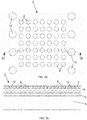
Figure 1a illustrates a portion of the surface of a semiconductor die, comprising an array of contact bumps and specifically placed solder bumps around the array.Figure 1b shows a cross section of the area shown inFigure 1a . -
Figure 2a illustrates a portion of the surface of a semiconductor wafer, comprising an array of contact pads and specifically placed contact areas around the array.Figure 2b shows a cross section of the area shown inFigure 2a . -
Figure 3 illustrates the alignment of the die fromFigure 1 to the wafer ofFigure 2 . -
Figure 4 illustrates the result of the bonding of the die to the wafer through soldering the solder bumps to the contact areas. - The invention will be described on the basis of an exemplary embodiment that does not limit the invention scope. According to the embodiment, a semiconductor die is bonded to a semiconductor wafer. The wafer comprises a plurality of processed dies, which are yet to be separated. The semiconductor die is to be bonded to one of these processed dies or a part thereof, to form a 3D stack of interconnected dies. Both these semiconductor components, the separate die and the wafer, comprise a number of contact structures on their surface, which may be metal contact bumps or contact pads.
-
Figures 1 and2 illustrate corresponding portions respectively of thedie 1 and of thewafer 2, which are to be bonded together. As well known to the skilled reader, both thedie 1 and thewafer 2 comprise asemiconductor substrate 3, most commonly a silicon substrate, and on top thereof a plurality of active devices such as transistors and diodes in the front end of line (FEOL)part 4, and a network of interconnect lines and vias embedded in a dielectric material in the back end of line (BEOL)part 5. The upper layer of theBEOL part 5 is shown in more detail and comprisescontact pads 6 embedded in the dielectric 7. The BEOL network is connected to a plurality of terminals on the surfaces of thedie 1 and of thewafer 2. In the case of thedie 1 shown inFigure 1 , the terminals appear in the form ofcontact structures 10 protruding outward from the surface of thecontact pads 6. These protruding contact structures will hereafter be referred to ascontact bumps 10. In the case of thewafer 2 shown inFigure 2 , the terminals are theactual contact pads 6 as such, lying essentially in the plane of the surface of thewafer 2. Planar contact pads could also be formed on top of theBEOL part 5 of thewafer 2. According to other embodiments, both components could be provided withcontact bumps 10 which are to be bonded to each other. The process described hereafter is applicable to the bonding of contact bumps to pads or bumps of the same metal, for example to establish a Cu-Cu bond, a Co-Co bond or a Ni-Ni bond. Bonding between different metals is not excluded from the scope of the invention, although this may require the addition of additives to the metals, such as catalyst metals like Au or Pt, added in the form of colloids. - The contact bumps 10 of the
die 1 are to be bonded to thecontact pads 6 on thewafer 2, by the direct metal-metal bond. As stated above, realizing such a bond requires a long process which is disadvantageous in terms of the process throughput, especially in the case of die-to-wafer bonding. - According to the invention, this problem is solved by providing additional bonding structures on the components. In the case shown in the drawings, the
die 1 is provided with a number of solder bumps 11, while thewafer 2 is provided withcontact areas 12 corresponding to the locations of the solder bumps 11 when the die is aligned to the wafer. According to preferred embodiments, the solder bumps 11 andcontact areas 12 are dummy contact structures, i.e. they are not electrically connected to the FEOL parts and to the BEOL networks of the respective components, as they primarily serve another purpose, namely to establish a fast solder bond between thecomponents bumps 10 and thecontact pads 6. The actual metal-metal bond is realized in a subsequent heating step. - As illustrated in
Figure 3 , thedie 1 is aligned to thewafer 2, by aligning the solder bumps 11 to thecontact areas 12, and the contact bumps 10 to thecontact pads 6. Thedie 1 is lowered towards thewafer 2 so that the solder bumps 11 are in physical contact with the contact areas 12 (seeFigure 4 ), at which point the solder bumps 11 are pressed to thecontact areas 12 and the temperature is rapidly raised above the melting point of the solder material so that the solder melts and forms asolder connection 13 consisting fully or for the most part of an intermetallic compound (IMC) when the temperature is again lowered. The IMC is a compound of the solder metal with the metal of thecontact area 12 and/or of thepad 6 of the die onto which thesolder bump 10 is placed. This process is known as the TCB process (Thermocompression bonding). This is therefore a solder process as known in the art, and the process can be executed according to well-known practice and using existing processing tools. As known to the skilled person, this soldering process is fast, and may be realized in the order of seconds, for example in about 5s for most of the known combinations of solder metal and metals of thecontact areas 12 and of thecontact pads 6. Any of such known combinations may be used in the method of the invention. The melting temperature of the solder is lower than the melting temperature of the metal used for the metal contact bumps 10 and thecorresponding contact pads 6. - Due to the melting of the solder, the solidified
solder connections 13 are of lower height than the initial height of the solder bumps 11. As shown in the drawings, said initial height of the solder bumps 11 is chosen to be higher than the height of the metal contact bumps 10, so that after the soldering process, these contact bumps 10 of thedie 1 are in physical contact with thecontact pads 6 of thewafer 2. For example, the height of the solder bumps 11 may be 5 micrometer, with the metal bumps 10 having a height of 3 micrometer. These heights and the pressure applied during TCB bonding are configured so that after the soldering process, the metal bumps 10 of the die and the metal pads of the wafer form a so-called 'cold joint'. The metal-metal bond is not realized at this point, as this requires a prolonged heating process in order to obtain the required interdiffusion of the metal of thebumps 10 and thecontact pads 6. According to the invention, the heating process for establishing the metal-metal bonds takes place after the soldering process. However, because thesolder connections 13 have already bonded thedie 1 to thewafer 2, this heating process does not need to be performed separately for each die. Several dies can be bonded to the wafer using the above-described soldering approach, followed by a heating process for realizing the metal-metal bonds between the plurality of dies and the wafer. The heating process may for example be performed by heating the assembly of the wafer and several dies to a temperature of about 300°C for a period of about one hour. - This approach thereby enables to increase the throughput of the die-to-wafer bonding process, as only one heating process is required to establish the metal-metal bonds between the wafer and a plurality of dies, whereas in the prior art, the heating process was required separately for each die.
- The heating step could be performed in the same tool as the soldering step, or in a different tool, for example by moving the assembly of the
wafer 2 and thedie 1 to a heating oven and applying the heat treatment in that oven. This furthermore enables subjecting multiple assemblies of wafers having one or more dies pre-bonded to them through the above-described soldering step to the heating step by loading a batch of such wafers into the oven. - The method of the invention can also be applied for bonding a wafer to another wafer. The above-described batch could thus also comprise one or more wafer-wafer assemblies.
- The intermetallic compound must have a higher melting point than the temperature applied during the heating step, which is the case in most soldering processes. In this way, the IMC does not melt during the heating step performed according to the invention, after the soldering step. If the
solder connections 13 still comprise a small amount of solder material, this amount will melt during the heating step, but this is allowable and will even be helpful in pulling the components together. - As seen in the drawings, the diameter of the solder bumps 11 is preferably higher than the diameter of the metal bumps 10. According to preferred embodiments, the surface area of the solder bumps 11 and the
contact areas 12 is chosen sufficiently high so as to enable the ability of the molten solder material to realize an auto-alignment of thedie 1 to thewafer 2, due to capillary forces generated by the liquid solder material, which will automatically cause the solder bumps 11 to align to thecontact areas 12. - Because of the auto-alignment aspect, the invention is particularly advantageous for realizing bonds between arrays of contact bumps 10 and
contact pads 6 with very low diameter and pitch, for example in the order of a 10-micron pitch or less. - The invention is not limited to the example shown in the drawings, where a number of solder bumps 11 are placed specifically around a group of contact bumps 10. The solder bumps 11 could be distributed more randomly across the surfaces of the
components pitched contact bumps 10, represents a preferred embodiment of the invention. The solder bumps 11 are not necessarily placed on the component provided with contact bumps 10, but could instead be provided on the other component. - According to preferred embodiments, a dielectric underfill material is applied that fills up the gaps between the interconnected solder bumps and metal contact bumps. The underfill may be applied before bonding, or after the soldering step and before the heating step. The methods for applying the underfill in both cases, and suitable underfill materials are known in the art and may be applied as such in the invention.
- The invention is also applicable to the stacking of multiple dies, one on top of the other.
Figure 5 illustrates an embodiment wherein two dies are stacked on thewafer 1. Thefirst die 1 is now provided withTSV connections 15 through thesubstrate 3, which connect the contact bumps 10 to contactpads 6 on the back side of thedie 1. Also,dummy contact areas 12 are provided on the backside of thedie 1. Thecontact pads 6 and thedummy contact areas 12 on the back side of thedie 1 are configured to receive respectively the metal contact bumps 10 and dummy solder bumps 11 of thesecond die 20, which is to be bonded to the backside of thefirst die 1. According to the invention, the sequence is as follows: - Aligning the
first die 1 to thewafer 2 and realizing thesolder connections 13, - Aligning the
second die 20 to thefirst die 1 and realizing solder connections between the solder bumps 11 of thesecond die 20 and thecontact areas 12 on the back side of thefirst die 1, - Heating the assembly of the
wafer 2 and the two dies 1 and 20 to a bonding temperature to establish metal-metal bonds between thefirst die 1 and thewafer 2 and between thesecond die 20 and thefirst die 1. - The stack may comprise more than two dies. The final heating step takes place after all the dies have been bonded by the respective solder connections.
- While the invention has been illustrated and described in detail in the drawings and foregoing description, such illustration and description are to be considered illustrative or exemplary and not restrictive. Other variations to the disclosed embodiments can be understood and effected by those skilled in the art in practicing the claimed invention, from a study of the drawings, the disclosure and the appended claims. In the claims, the word "comprising" does not exclude other elements or steps, and the indefinite article "a" or "an" does not exclude a plurality. The mere fact that certain measures are recited in mutually different dependent claims does not indicate that a combination of these measures cannot be used to advantage. Any reference signs in the claims should not be construed as limiting the scope.
Claims (10)
- A method for bonding a first semiconductor component (1) to a second semiconductor component (2), at least one of the components comprising a plurality of protruding metal contact structures (10), by bonding said plurality of protruding contact structures to corresponding protruding metal contact structures or metal contacts pads (6) on the other component, the bonding taking place by direct metal to metal contact bonding,
characterized in that:- one of the components is provided with a plurality of solder bumps (11) for establishing solder connections (13) between the solder bumps (11) and corresponding contact areas (12) provided on the other component,- The bonding process comprises the steps of :∘ aligning the components (1,2) so that the solder bumps (11) are aligned to the corresponding contact areas (12),∘ realising said solder connections (13) between the corresponding solders bumps (11) and contact areas (12), wherein the solder bumps (11) and contact areas (12) are configured so that the protruding metal contact structures (10) of one of the components are in physical contact with the corresponding protruding metal contact structures or the metal pads (6) of the other component while not forming a metal bond, when the solder connections (13) are established, thereby obtaining an assembly of the first and second component (1,2) bonded only through the solder connections (13),∘ subjecting the assembly to a heat treatment for bonding the protruding metal contact structures (10) to the corresponding metal structures or pads (6). - The method according to claim 1, wherein the surface area of the solder bumps (11) and the contact areas (12) is chosen so that during the soldering process applied for realising the solder connections, the molten solder material enhances the alignment of the solder bumps (11) to the contact areas (12) due to a self-aligning influence of the capillary forces exhibited by the molten material on the solder bumps (11) and the contact areas (12).
- The method according to claim 2, wherein the surface area of the solder bumps (11) is higher than the surface area of the metal contact structures (10).
- The method according to any one of claims 1 to 3, wherein the first component is a semiconductor die (1), and the second component is a semiconductor wafer (2).
- The method according to claim 4, wherein a plurality of dies (1) are bonded to the wafer (2) through said steps of aligning and establishing solder connections (13), and wherein the step of subjecting the assembly to a heat treatment is performed simultaneously for the plurality of dies (1).
- The method according to claim 4 or 5, wherein a plurality of dies are bonded in at least one stack, a first die (1) being bonded to the wafer (2) through said steps of aligning and establishing solder connections (13), and one or more additional dies (20) being bonded to the back side of preceding dies through said steps of aligning and establishing solder connections (13), and wherein the step of subjecting the assembly to a heat treatment is performed simultaneously for the at least one stack of dies.
- The method according to any one of the preceding claims, wherein the solder bumps (11) are dummy solder bumps.
- The method according to any one of the preceding claims, wherein the protruding metal contact structures (10) and corresponding pads (6) are arranged in a two-dimensional array, and wherein the solder bumps (11) and corresponding contact areas (12) are located around the respective arrays.
- The method according to any one of the preceding claims, wherein the protruding metal contact structures (10) and the corresponding metal structures or pads (6) are formed of the same metal.
- The method according to any one of the preceding claims, wherein a dielectric underfill material is applied that fills the gaps between the solder connections (13) and the bonded metal protrusions (10).
Priority Applications (2)
| Application Number | Priority Date | Filing Date | Title |
|---|---|---|---|
| EP19211529.3A EP3828922A1 (en) | 2019-11-26 | 2019-11-26 | A method for bonding semiconductor components |
| US17/102,249 US11810892B2 (en) | 2019-11-26 | 2020-11-23 | Method of direct bonding semiconductor components |
Applications Claiming Priority (1)
| Application Number | Priority Date | Filing Date | Title |
|---|---|---|---|
| EP19211529.3A EP3828922A1 (en) | 2019-11-26 | 2019-11-26 | A method for bonding semiconductor components |
Publications (1)
| Publication Number | Publication Date |
|---|---|
| EP3828922A1 true EP3828922A1 (en) | 2021-06-02 |
Family
ID=68731678
Family Applications (1)
| Application Number | Title | Priority Date | Filing Date |
|---|---|---|---|
| EP19211529.3A Pending EP3828922A1 (en) | 2019-11-26 | 2019-11-26 | A method for bonding semiconductor components |
Country Status (2)
| Country | Link |
|---|---|
| US (1) | US11810892B2 (en) |
| EP (1) | EP3828922A1 (en) |
Cited By (2)
| Publication number | Priority date | Publication date | Assignee | Title |
|---|---|---|---|---|
| US11562975B2 (en) | 2021-04-29 | 2023-01-24 | Sandisk Technologies Llc | Bonded assembly employing metal-semiconductor bonding and metal-metal bonding and methods of forming the same |
| US12068282B2 (en) | 2021-08-18 | 2024-08-20 | Micron Technology, Inc. | Hybrid metallic structures in stacked semiconductor devices and associated systems and methods |
Families Citing this family (6)
| Publication number | Priority date | Publication date | Assignee | Title |
|---|---|---|---|---|
| US10847485B2 (en) | 2018-12-21 | 2020-11-24 | Taiwan Semiconductor Manufacturing Co., Ltd. | Chip package structure and method for forming the same |
| JP7524632B2 (en) * | 2020-06-29 | 2024-07-30 | 日本電気株式会社 | Quantum Devices |
| JP2024153958A (en) * | 2021-09-02 | 2024-10-30 | キオクシア株式会社 | Semiconductor device and method for manufacturing the same |
| US20230386988A1 (en) * | 2022-05-31 | 2023-11-30 | Taiwan Semiconductor Manufacturing Company Limited | Semiconductor package with variable pillar height and methods for forming the same |
| CN118458690A (en) * | 2024-05-28 | 2024-08-09 | 山东产研微纳与智能制造研究院有限公司 | Method for improving wafer bonding alignment precision based on liquid surface tension |
| CN119673787B (en) * | 2024-12-10 | 2025-06-24 | 北京芯力技术创新中心有限公司 | Chip stacking method on wafer and semiconductor device |
Citations (4)
| Publication number | Priority date | Publication date | Assignee | Title |
|---|---|---|---|---|
| JP2004253598A (en) * | 2003-02-20 | 2004-09-09 | Fujitsu Ltd | Electronic component mounting method |
| US20170025387A1 (en) * | 2015-07-24 | 2017-01-26 | Shinko Electric Industries Co., Ltd. | Packaging structure |
| US9754893B2 (en) * | 2014-09-29 | 2017-09-05 | Semiconductor Manufacturing International (Shanghai) Corporation | Semiconductor structure and fabrication method thereof |
| US10014235B2 (en) * | 2014-03-07 | 2018-07-03 | Nitto Denko Corporation | Underfill material, laminated sheet and method for producing semiconductor device |
Family Cites Families (7)
| Publication number | Priority date | Publication date | Assignee | Title |
|---|---|---|---|---|
| US7041533B1 (en) | 2000-06-08 | 2006-05-09 | Micron Technology, Inc. | Stereolithographic method for fabricating stabilizers for semiconductor devices |
| US6870270B2 (en) | 2002-12-28 | 2005-03-22 | Intel Corporation | Method and structure for interfacing electronic devices |
| US8030761B2 (en) * | 2007-05-23 | 2011-10-04 | United Test And Assembly Center Ltd. | Mold design and semiconductor package |
| US20110084375A1 (en) | 2009-10-13 | 2011-04-14 | Freescale Semiconductor, Inc | Semiconductor device package with integrated stand-off |
| JP6221499B2 (en) | 2013-08-19 | 2017-11-01 | 富士通株式会社 | Electronic device and method of manufacturing electronic device |
| US9570421B2 (en) | 2013-11-14 | 2017-02-14 | Taiwan Semiconductor Manufacturing Co., Ltd. | Stacking of multiple dies for forming three dimensional integrated circuit (3DIC) structure |
| TWI578697B (en) | 2015-12-07 | 2017-04-11 | 穩懋半導體股份有限公司 | Protective structure for semiconductor component package |
-
2019
- 2019-11-26 EP EP19211529.3A patent/EP3828922A1/en active Pending
-
2020
- 2020-11-23 US US17/102,249 patent/US11810892B2/en active Active
Patent Citations (4)
| Publication number | Priority date | Publication date | Assignee | Title |
|---|---|---|---|---|
| JP2004253598A (en) * | 2003-02-20 | 2004-09-09 | Fujitsu Ltd | Electronic component mounting method |
| US10014235B2 (en) * | 2014-03-07 | 2018-07-03 | Nitto Denko Corporation | Underfill material, laminated sheet and method for producing semiconductor device |
| US9754893B2 (en) * | 2014-09-29 | 2017-09-05 | Semiconductor Manufacturing International (Shanghai) Corporation | Semiconductor structure and fabrication method thereof |
| US20170025387A1 (en) * | 2015-07-24 | 2017-01-26 | Shinko Electric Industries Co., Ltd. | Packaging structure |
Cited By (2)
| Publication number | Priority date | Publication date | Assignee | Title |
|---|---|---|---|---|
| US11562975B2 (en) | 2021-04-29 | 2023-01-24 | Sandisk Technologies Llc | Bonded assembly employing metal-semiconductor bonding and metal-metal bonding and methods of forming the same |
| US12068282B2 (en) | 2021-08-18 | 2024-08-20 | Micron Technology, Inc. | Hybrid metallic structures in stacked semiconductor devices and associated systems and methods |
Also Published As
| Publication number | Publication date |
|---|---|
| US20210159207A1 (en) | 2021-05-27 |
| US11810892B2 (en) | 2023-11-07 |
Similar Documents
| Publication | Publication Date | Title |
|---|---|---|
| US11810892B2 (en) | Method of direct bonding semiconductor components | |
| US6221753B1 (en) | Flip chip technique for chip assembly | |
| US20210175194A1 (en) | Bond pad with micro-protrusions for direct metallic bonding | |
| US8759972B2 (en) | Semiconductor device and method of forming composite bump-on-lead interconnection | |
| US9263426B2 (en) | PoP structure with electrically insulating material between packages | |
| JP3186941B2 (en) | Semiconductor chips and multi-chip semiconductor modules | |
| US20090258459A1 (en) | Packaged System of Semiconductor Chips Having a Semiconductor Interposer | |
| US7745258B2 (en) | Manufacturing method of semiconductor device | |
| US7026188B2 (en) | Electronic device and method for manufacturing the same | |
| US9496154B2 (en) | Use of underfill tape in microelectronic components, and microelectronic components with cavities coupled to through-substrate vias | |
| US10651151B2 (en) | 3D integration using Al—Ge eutectic bond interconnect | |
| US11935824B2 (en) | Integrated circuit package module including a bonding system | |
| US9679875B2 (en) | Reduced volume interconnect for three-dimensional chip stack | |
| US9349705B2 (en) | Method of fabricating a semiconductor structure having conductive bumps with a plurality of metal layers | |
| US6489180B1 (en) | Flip-chip packaging process utilizing no-flow underfill technique | |
| US9425174B1 (en) | Integrated circuit package with solderless interconnection structure | |
| EP2075828A1 (en) | Semiconductor device and a method for aligining and bonding a first and second element for the fabrication of a semiconductor device | |
| JP2000286304A (en) | Semiconductor element manufacturing method, semiconductor element, semiconductor device manufacturing method, semiconductor device, and mounting module | |
| CN112908873A (en) | Semiconductor module assembling method, semiconductor module and electronic device | |
| CN117747556A (en) | Packaging structure with adhesive layer and packaging method thereof | |
| JP2002170847A (en) | Semiconductor device manufacturing method and semiconductor device | |
| USRE44500E1 (en) | Semiconductor device and method of forming composite bump-on-lead interconnection | |
| KR101053746B1 (en) | Semiconductor system and manufacturing method thereof | |
| US20250118691A1 (en) | Semiconductor Component Comprising Structured Contacts and A Method for Producing the Component | |
| US9589877B2 (en) | Semiconductor device and method for manufacturing the same |
Legal Events
| Date | Code | Title | Description |
|---|---|---|---|
| PUAI | Public reference made under article 153(3) epc to a published international application that has entered the european phase |
Free format text: ORIGINAL CODE: 0009012 |
|
| STAA | Information on the status of an ep patent application or granted ep patent |
Free format text: STATUS: THE APPLICATION HAS BEEN PUBLISHED |
|
| AK | Designated contracting states |
Kind code of ref document: A1 Designated state(s): AL AT BE BG CH CY CZ DE DK EE ES FI FR GB GR HR HU IE IS IT LI LT LU LV MC MK MT NL NO PL PT RO RS SE SI SK SM TR |
|
| STAA | Information on the status of an ep patent application or granted ep patent |
Free format text: STATUS: REQUEST FOR EXAMINATION WAS MADE |
|
| 17P | Request for examination filed |
Effective date: 20211201 |
|
| RBV | Designated contracting states (corrected) |
Designated state(s): AL AT BE BG CH CY CZ DE DK EE ES FI FR GB GR HR HU IE IS IT LI LT LU LV MC MK MT NL NO PL PT RO RS SE SI SK SM TR |