EP3824466B1 - A refresh scheme in a memory controller - Google Patents
A refresh scheme in a memory controller Download PDFInfo
- Publication number
- EP3824466B1 EP3824466B1 EP19837001.7A EP19837001A EP3824466B1 EP 3824466 B1 EP3824466 B1 EP 3824466B1 EP 19837001 A EP19837001 A EP 19837001A EP 3824466 B1 EP3824466 B1 EP 3824466B1
- Authority
- EP
- European Patent Office
- Prior art keywords
- refresh
- memory
- accesses
- command
- type
- Prior art date
- Legal status (The legal status is an assumption and is not a legal conclusion. Google has not performed a legal analysis and makes no representation as to the accuracy of the status listed.)
- Active
Links
Images



Classifications
-
- G—PHYSICS
- G06—COMPUTING OR CALCULATING; COUNTING
- G06F—ELECTRIC DIGITAL DATA PROCESSING
- G06F13/00—Interconnection of, or transfer of information or other signals between, memories, input/output devices or central processing units
- G06F13/14—Handling requests for interconnection or transfer
- G06F13/16—Handling requests for interconnection or transfer for access to memory bus
- G06F13/1605—Handling requests for interconnection or transfer for access to memory bus based on arbitration
- G06F13/161—Handling requests for interconnection or transfer for access to memory bus based on arbitration with latency improvement
- G06F13/1636—Handling requests for interconnection or transfer for access to memory bus based on arbitration with latency improvement using refresh
-
- G—PHYSICS
- G06—COMPUTING OR CALCULATING; COUNTING
- G06F—ELECTRIC DIGITAL DATA PROCESSING
- G06F13/00—Interconnection of, or transfer of information or other signals between, memories, input/output devices or central processing units
- G06F13/14—Handling requests for interconnection or transfer
- G06F13/16—Handling requests for interconnection or transfer for access to memory bus
- G06F13/1605—Handling requests for interconnection or transfer for access to memory bus based on arbitration
- G06F13/1642—Handling requests for interconnection or transfer for access to memory bus based on arbitration with request queuing
-
- G—PHYSICS
- G06—COMPUTING OR CALCULATING; COUNTING
- G06F—ELECTRIC DIGITAL DATA PROCESSING
- G06F13/00—Interconnection of, or transfer of information or other signals between, memories, input/output devices or central processing units
- G06F13/14—Handling requests for interconnection or transfer
- G06F13/16—Handling requests for interconnection or transfer for access to memory bus
- G06F13/18—Handling requests for interconnection or transfer for access to memory bus based on priority control
-
- G—PHYSICS
- G06—COMPUTING OR CALCULATING; COUNTING
- G06F—ELECTRIC DIGITAL DATA PROCESSING
- G06F3/00—Input arrangements for transferring data to be processed into a form capable of being handled by the computer; Output arrangements for transferring data from processing unit to output unit, e.g. interface arrangements
- G06F3/06—Digital input from, or digital output to, record carriers, e.g. RAID, emulated record carriers or networked record carriers
- G06F3/0601—Interfaces specially adapted for storage systems
- G06F3/0628—Interfaces specially adapted for storage systems making use of a particular technique
- G06F3/0655—Vertical data movement, i.e. input-output transfer; data movement between one or more hosts and one or more storage devices
- G06F3/0658—Controller construction arrangements
-
- G—PHYSICS
- G06—COMPUTING OR CALCULATING; COUNTING
- G06F—ELECTRIC DIGITAL DATA PROCESSING
- G06F3/00—Input arrangements for transferring data to be processed into a form capable of being handled by the computer; Output arrangements for transferring data from processing unit to output unit, e.g. interface arrangements
- G06F3/06—Digital input from, or digital output to, record carriers, e.g. RAID, emulated record carriers or networked record carriers
- G06F3/0601—Interfaces specially adapted for storage systems
- G06F3/0628—Interfaces specially adapted for storage systems making use of a particular technique
- G06F3/0655—Vertical data movement, i.e. input-output transfer; data movement between one or more hosts and one or more storage devices
- G06F3/0659—Command handling arrangements, e.g. command buffers, queues, command scheduling
-
- G—PHYSICS
- G11—INFORMATION STORAGE
- G11C—STATIC STORES
- G11C11/00—Digital stores characterised by the use of particular electric or magnetic storage elements; Storage elements therefor
- G11C11/21—Digital stores characterised by the use of particular electric or magnetic storage elements; Storage elements therefor using electric elements
- G11C11/34—Digital stores characterised by the use of particular electric or magnetic storage elements; Storage elements therefor using electric elements using semiconductor devices
- G11C11/40—Digital stores characterised by the use of particular electric or magnetic storage elements; Storage elements therefor using electric elements using semiconductor devices using transistors
- G11C11/401—Digital stores characterised by the use of particular electric or magnetic storage elements; Storage elements therefor using electric elements using semiconductor devices using transistors forming cells needing refreshing or charge regeneration, i.e. dynamic cells
- G11C11/406—Management or control of the refreshing or charge-regeneration cycles
- G11C11/40603—Arbitration, priority and concurrent access to memory cells for read/write or refresh operations
-
- G—PHYSICS
- G11—INFORMATION STORAGE
- G11C—STATIC STORES
- G11C11/00—Digital stores characterised by the use of particular electric or magnetic storage elements; Storage elements therefor
- G11C11/21—Digital stores characterised by the use of particular electric or magnetic storage elements; Storage elements therefor using electric elements
- G11C11/34—Digital stores characterised by the use of particular electric or magnetic storage elements; Storage elements therefor using electric elements using semiconductor devices
- G11C11/40—Digital stores characterised by the use of particular electric or magnetic storage elements; Storage elements therefor using electric elements using semiconductor devices using transistors
- G11C11/401—Digital stores characterised by the use of particular electric or magnetic storage elements; Storage elements therefor using electric elements using semiconductor devices using transistors forming cells needing refreshing or charge regeneration, i.e. dynamic cells
- G11C11/406—Management or control of the refreshing or charge-regeneration cycles
- G11C11/40611—External triggering or timing of internal or partially internal refresh operations, e.g. auto-refresh or CAS-before-RAS triggered refresh
-
- G—PHYSICS
- G11—INFORMATION STORAGE
- G11C—STATIC STORES
- G11C11/00—Digital stores characterised by the use of particular electric or magnetic storage elements; Storage elements therefor
- G11C11/21—Digital stores characterised by the use of particular electric or magnetic storage elements; Storage elements therefor using electric elements
- G11C11/34—Digital stores characterised by the use of particular electric or magnetic storage elements; Storage elements therefor using electric elements using semiconductor devices
- G11C11/40—Digital stores characterised by the use of particular electric or magnetic storage elements; Storage elements therefor using electric elements using semiconductor devices using transistors
- G11C11/401—Digital stores characterised by the use of particular electric or magnetic storage elements; Storage elements therefor using electric elements using semiconductor devices using transistors forming cells needing refreshing or charge regeneration, i.e. dynamic cells
- G11C11/406—Management or control of the refreshing or charge-regeneration cycles
- G11C11/40618—Refresh operations over multiple banks or interleaving
-
- G—PHYSICS
- G11—INFORMATION STORAGE
- G11C—STATIC STORES
- G11C11/00—Digital stores characterised by the use of particular electric or magnetic storage elements; Storage elements therefor
- G11C11/21—Digital stores characterised by the use of particular electric or magnetic storage elements; Storage elements therefor using electric elements
- G11C11/34—Digital stores characterised by the use of particular electric or magnetic storage elements; Storage elements therefor using electric elements using semiconductor devices
- G11C11/40—Digital stores characterised by the use of particular electric or magnetic storage elements; Storage elements therefor using electric elements using semiconductor devices using transistors
- G11C11/401—Digital stores characterised by the use of particular electric or magnetic storage elements; Storage elements therefor using electric elements using semiconductor devices using transistors forming cells needing refreshing or charge regeneration, i.e. dynamic cells
- G11C11/4063—Auxiliary circuits, e.g. for addressing, decoding, driving, writing, sensing or timing
- G11C11/407—Auxiliary circuits, e.g. for addressing, decoding, driving, writing, sensing or timing for memory cells of the field-effect type
- G11C11/4076—Timing circuits
-
- G—PHYSICS
- G11—INFORMATION STORAGE
- G11C—STATIC STORES
- G11C11/00—Digital stores characterised by the use of particular electric or magnetic storage elements; Storage elements therefor
- G11C11/21—Digital stores characterised by the use of particular electric or magnetic storage elements; Storage elements therefor using electric elements
- G11C11/34—Digital stores characterised by the use of particular electric or magnetic storage elements; Storage elements therefor using electric elements using semiconductor devices
- G11C11/40—Digital stores characterised by the use of particular electric or magnetic storage elements; Storage elements therefor using electric elements using semiconductor devices using transistors
- G11C11/401—Digital stores characterised by the use of particular electric or magnetic storage elements; Storage elements therefor using electric elements using semiconductor devices using transistors forming cells needing refreshing or charge regeneration, i.e. dynamic cells
- G11C11/406—Management or control of the refreshing or charge-regeneration cycles
- G11C11/40615—Internal triggering or timing of refresh, e.g. hidden refresh, self refresh, pseudo-SRAMs
Definitions
- DRAM dynamic random-access memory
- DDR double data rate
- JEDEC Joint Electron Devices Engineering Council
- DRAM chips are not persistent memory devices. Therefore, periodic memory refresh is needed by the DRAM chips for data retention during normal operation of the computer system.
- Memory refresh is a background maintenance process required during operation of semiconductor DRAM. Each bit of memory data is stored as the presence or absence of an electric charge on small capacitors which form the DRAM chips. Charges on the capacitors leak away over time, and without a memory refresh, stored data will be lost.
- external circuitry sends commands to cause the memory to periodically read a row and rewrite the row, restoring the charges on the capacitors of the memory cells of the row to the original charge level. While refresh is occurring, the memory is not available for normal read and write operations.
- US 2018/018133 discloses a data processing system with a memory controller having a refresh logic circuit that generates refresh requests separate from normal read and write memory access requests, and an arbiter that arbitrates between normal read and write memory access requests stored in a command queue and the refresh requests generated by the refresh logic circuit.
- US 2018/018291 A1 discloses a memory controller having three sub-arbiters for different types of page statuses, and a final arbiter that selects between three sub-arbitration winners as well as a refresh operation from refresh logic that generates autorefresh commands periodically.
- the invention provides a memory controller in accordance with claim 1, a data processing system in accordance with claim 8, and a method for managing refresh of a memory in a memory system in accordance with claim 9.
- a memory controller includes a command queue, an arbiter, a refresh logic circuit, and a final arbiter.
- the command queue receives and stores memory access requests for a memory.
- the arbiter selectively picks accesses from the command queue according to a first type of accesses and a second type of accesses. The first type of accesses and the second type of accesses correspond to different page statuses of corresponding memory accesses in the memory.
- the refresh logic circuit generates a refresh command to a bank of the memory.
- the refresh logic circuit provides a priority indicator with the refresh command whose value is set according to a number of pending refreshes.
- the final arbiter selectively orders the refresh command with respect to memory access requests of the first type accesses and the second type accesses. The ordering is based on the priority indicator.
- a data processing system in another form, includes a memory accessing agent, a memory system, and a memory controller.
- the memory accessing agent provides memory access requests for a memory.
- the memory system is coupled to the memory accessing agent.
- the memory controller is coupled to the memory system and the memory accessing agent includes a command queue, an arbiter, and a final arbiter.
- the command queue stores memory access commands received from the memory accessing agent.
- the arbiter selectively picks memory accesses from the command queue according to a first type of access and a second type of access. Each type of access corresponds to a different page status of a bank in the memory.
- the final arbiter arbitrates based on input received from a refresh logic circuit.
- the refresh logic circuit generates a refresh command to the bank of the memory and provides a priority indicator to the refresh command.
- the value of the priority indicator is set according to a number of pending refreshes, to selectively order the refresh command with respect to a first type of access and a second type of access.
- a method for managing refresh of a memory in a memory system via a memory controller A plurality of memory access requests is received and stored in a command queue. The memory accesses requests are selectively picked from the command queue according to a first type of accesses and a second type of accesses. The first type of accesses and a second type of accesses correspond to different page statuses of corresponding memory accesses in the memory.
- a refresh command is generated to a bank of the memory.
- a priority indicator is provided with the refresh command. The refresh command is selectively ordered with respect to memory access requests of the first type access and the second type access based on the priority indicator.
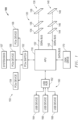
- FIG. 1 illustrates in block diagram form a data processing system 100 according to some embodiments.
- Data processing system 100 includes generally a data processor 110 in the form of an accelerated processing unit (APU), a memory system 120, a peripheral component interconnect express (PCIe) system 150, a universal serial bus (USB) system 160, and a disk drive 170.
- Data processor 110 operates as the central processing unit (CPU) of data processing system 100 and provides various buses and interfaces useful in modern computer systems. These interfaces include two double data rate (DDRx) memory channels, a PCIe root complex for connection to a PCIe link, a USB controller for connection to a USB network, and an interface to a Serial Advanced Technology Attachment (SATA) mass storage device.
- DDRx double data rate
- PCIe root complex for connection to a PCIe link
- USB controller for connection to a USB network
- SATA Serial Advanced Technology Attachment
- Memory system 120 includes a memory channel 130 and a memory channel 140.
- Memory channel 130 includes a set of dual inline memory modules (DIMMs) connected to a DDRx bus 132, including representative DIMMs 134, 136, and 138 that in this example correspond to separate ranks.
- memory channel 140 includes a set of DIMMs connected to a DDRx bus 142, including representative DIMMs 144, 146, and 148.
- PCIe system 150 includes a PCIe switch 152 connected to the PCIe root complex in data processor 110, a PCIe device 154, a PCIe device 156, and a PCIe device 158.
- PCIe device 156 in turn is connected to a system basic input/output system (BIOS) memory 157.
- BIOS memory 157 can be any of a variety of non-volatile memory types, such as read-only memory (ROM), flash electrically erasable programmable ROM (EEPROM), and the like.
- USB system 160 includes a USB hub 162 connected to a USB master in data processor 110, and representative USB devices 164, 166, and 168 each connected to USB hub 162.
- USB devices 164, 166, and 168 could be devices such as a keyboard, a mouse, a flash EEPROM port, and the like.
- Disk drive 170 is connected to data processor 110 over a SATA bus and provides mass storage for the operating system, application programs, application files, and the like.
- Data processing system 100 is suitable for use in modem computing applications by providing a memory channel 130 and a memory channel 140.
- Each of memory channels 130 and 140 can connect to state-of-the-art DDR memories such as DDR version four (DDR4), low power DDR4 (LPDDR4), graphics DDR version five (GDDR5), and high bandwidth memory (HBM), and can be adapted for future memory technologies.
- DDR4 DDR version four
- LPDDR4 low power DDR4
- GDDR5 graphics DDR version five
- HBM high bandwidth memory
- FIG. 2 illustrates in block diagram form an APU 200 suitable for use in data processing system 100 of FIG. 1 .
- APU 200 includes generally a central processing unit (CPU) core complex 210, a graphics core 220, a set of display engines 230, a memory management hub 240, a data fabric 250, a set of peripheral controllers 260, a set of peripheral bus controllers 270, a system management unit (SMU) 280, and a set of memory controllers 290.
- CPU central processing unit
- graphics core 220 for use in data processing system 100 of FIG. 1
- graphics core complex 210 includes generally a graphics core complex 210, a graphics core 220, a set of display engines 230, a memory management hub 240, a data fabric 250, a set of peripheral controllers 260, a set of peripheral bus controllers 270, a system management unit (SMU) 280, and a set of memory controllers 290.
- SMU system management unit
- CPU core complex 210 includes a CPU core 212 and a CPU core 214.
- CPU core complex 210 includes two CPU cores, but in other embodiments CPU core complex 210 can include an arbitrary number of CPU cores.
- Each of CPU cores 212 and 214 is bidirectionally connected to a system management network (SMN), which forms a control fabric, and to data fabric 250, and is capable of providing memory access requests to data fabric 250.
- SSN system management network
- Each of CPU cores 212 and 214 may be unitary cores, or may further be a core complex with two or more unitary cores sharing certain resources such as caches.
- Graphics core 220 is a high performance graphics processing unit (GPU) capable of performing graphics operations such as vertex processing, fragment processing, shading, texture blending, and the like in a highly integrated and parallel fashion. Graphics core 220 is bidirectionally connected to the SMN and to data fabric 250, and is capable of providing memory access requests to data fabric 250.
- APU 200 may either support a unified memory architecture in which CPU core complex 210 and graphics core 220 share the same memory space, or a memory architecture in which CPU core complex 210 and graphics core 220 share a portion of the memory space, while graphics core 220 also uses a private graphics memory not accessible by CPU core complex 210.
- Display engines 230 render and rasterize objects generated by graphics core 220 for display on a monitor. Graphics core 220 and display engines 230 are bidirectionally connected to a common memory management hub 240 for uniform translation into appropriate addresses in memory system 120, and memory management hub 240 is bidirectionally connected to data fabric 250 for generating such memory accesses and receiving read data returned from the memory system.
- Data fabric 250 includes a crossbar switch for routing memory access requests and memory responses between any memory accessing agent and memory controllers 290. It also includes a system memory map, defined by BIOS, for determining destinations of memory accesses based on the system configuration, as well as buffers for each virtual connection.
- BIOS system memory map
- Peripheral controllers 260 include a USB controller 262 and a SATA interface controller 264, each of which is bidirectionally connected to a system hub 266 and to the SMN bus. These two controllers are merely exemplary of peripheral controllers that may be used in APU 200.
- Peripheral bus controllers 270 include a system controller or "Southbridge” (SB) 272 and a PCIe controller 274, each of which is bidirectionally connected to an input/output (I/O) hub 276 and to the SMN bus.
- I/O hub 276 is also bidirectionally connected to system hub 266 and to data fabric 250.
- a CPU core can program registers in USB controller 262, SATA interface controller 264, SB 272, or PCIe controller 274 through accesses that data fabric 250 routes through I/O hub 276.
- SMU 280 is a local controller that controls the operation of the resources on APU 200 and synchronizes communication among them. SMU 280 manages power-up sequencing of the various processors on APU 200 and controls multiple off-chip devices via reset, enable and other signals. SMU 280 includes one or more clock sources not shown in FIG. 2 , such as a phase locked loop (PLL), to provide clock signals for each of the components of APU 200. SMU 280 also manages power for the various processors and other functional blocks, and may receive measured power consumption values from CPU cores 212 and 214 and graphics core 220 to determine appropriate power states.
- PLL phase locked loop
- APU 200 also implements various system monitoring and power saving functions.
- one system monitoring function is thermal monitoring. For example, if APU 200 becomes hot, then SMU 280 can reduce the frequency and voltage of CPU cores 212 and 214 and/or graphics core 220. If APU 200 becomes too hot, then it can be shut down entirely. Thermal events can also be received from external sensors by SMU 280 via the SMN bus, and SMU 280 can reduce the clock frequency and/or power supply voltage in response.
- FIG. 3 illustrates in block diagram form a memory controller 300 and an associated physical interface (PHY) 330 suitable for use in APU 200 of FIG. 2 according to some embodiments.
- Memory controller 300 includes a memory channel 310 and a power engine 320.
- Memory channel 310 includes a host interface 312, a memory channel controller 314, and a physical interface 316.
- Host interface 312 bidirectionally connects memory channel controller 314 to data fabric 250 over a scalable data port (SDP).
- SDP scalable data port
- Physical interface 316 bidirectionally connects memory channel controller 314 to PHY 330 over a bus that conforms to the DDR-PHY Interface Specification (DFI).
- DFI DDR-PHY Interface Specification
- Power engine 320 is bidirectionally connected to SMU 280 over the SMN bus, to PHY 330 over the Advanced Peripheral Bus (APB), and is also bidirectionally connected to memory channel controller 314.
- PHY 330 has a bidirectional connection to a memory channel such as memory channel 130 or memory channel 140 of FIG. 1 .
- Memory controller 300 is an instantiation of a memory controller for a single memory channel using a single memory channel controller 314, and has a power engine 320 to control operation of memory channel controller 314 in a manner that will be described further below.
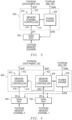
- FIG. 4 illustrates in block diagram form another memory controller 400 and associated PHYs 440 and 450 suitable for use in APU 200 of FIG. 2 according to some embodiments.
- Memory controller 400 includes memory channels 410 and 420 and a power engine 430.
- Memory channel 410 includes a host interface 412, a memory channel controller 414, and a physical interface 416.
- Host interface 412 bidirectionally connects memory channel controller 414 to data fabric 250 over an SDP.
- Physical interface 416 bidirectionally connects memory channel controller 414 to PHY 440, and conforms to the DFI Specification.
- Memory channel 420 includes a host interface 422, a memory channel controller 424, and a physical interface 426.
- Host interface 422 bidirectionally connects memory channel controller 424 to data fabric 250 over another SDP.
- Physical interface 426 bidirectionally connects memory channel controller 424 to PHY 450, and conforms to the DFI Specification.
- Power engine 430 is bidirectionally connected to SMU 280 over the SMN bus, to PHYs 440 and 450 over the APB, and is also bidirectionally connected to memory channel controllers 414 and 424.
- PHY 440 has a bidirectional connection to a memory channel such as memory channel 130 of FIG. 1 .
- PHY 450 has a bidirectional connection to a memory channel such as memory channel 140 of FIG. 1 .
- Memory controller 400 is an instantiation of a memory controller having two memory channel controllers and uses a shared power engine 430 to control operation of both memory channel controller 414 and memory channel controller 424 in a manner that will be described further below.
- FIG. 5 illustrates in block diagram form a memory controller 500 according to some embodiments.
- Memory controller 500 includes a memory channel controller 510 and a power controller 550.
- Memory channel controller 510 includes an interface 512, a queue 514, a command queue 520, an address generator 522, a content addressable memory (CAM) 524, a replay queue 530, a refresh logic circuit block 532, a timing block 534, a page table 536, an arbiter 538, an error correction code (ECC) check block 542, an ECC generation block 544, and a data buffer (DB) 546.
- ECC error correction code
- Interface 512 has a first bidirectional connection to data fabric 250 over an external bus, and has an output.
- this external bus is compatible with the advanced extensible interface version four specified by ARM Holdings, PLC of Cambridge, England, known as "AXI4", but can be other types of interfaces in other embodiments.
- Interface 512 translates memory access requests from a first clock domain known as the FCLK (or MEMCLK) domain to a second clock domain internal to memory controller 500 known as the UCLK domain.
- queue 514 provides memory accesses from the UCLK domain to the DFICLK domain associated with the DFI interface.
- Address generator 522 decodes addresses of memory access requests received from data fabric 250 over the AXI4 bus.
- the memory access requests include access addresses in the physical address space represented as a normalized address.
- Address generator 522 converts the normalized addresses into a format that can be used to address the actual memory devices in memory system 120, as well as to efficiently schedule related accesses. This format includes a region identifier that associates the memory access request with a particular rank, a row address, a column address, a bank address, and a bank group.
- the system BIOS queries the memory devices in memory system 120 to determine their size and configuration, and programs a set of configuration registers associated with address generator 522.
- Address generator 522 uses the configuration stored in the configuration registers to translate the normalized addresses into the appropriate format.
- Command queue 520 is a queue of memory access requests received from the memory accessing agents in data processing system 100, such as CPU cores 212 and 214 and graphics core 220.
- Command queue 520 stores the address fields decoded by address generator 522 as well other address information that allows arbiter 538 to select memory accesses efficiently, including access type and quality of service (QoS) identifiers.
- CAM 524 includes information to enforce ordering rules, such as write after write (WAW) and read after write (RAW) ordering rules.
- Replay queue 530 is a temporary queue for storing memory accesses picked by arbiter 538 that are awaiting responses, such as address and command parity responses, write cyclic redundancy check (CRC) responses for DDR4 DRAM or write and read CRC responses for GDDR5 DRAM.
- Replay queue 530 accesses ECC check block 542 to determine whether the returned ECC is correct or indicates an error. Replay queue 530 allows the accesses to be replayed in the case of a parity or CRC error of one of these cycles.
- Refresh logic circuit 532 includes state machines for various powerdown, refresh, and termination resistance (ZQ) calibration cycles that are generated separately from normal read and write memory access requests received from memory accessing agents. For example, if a memory rank is in precharge powerdown, it must be periodically awakened to run refresh cycles. Refresh logic circuit 532 generates auto-refresh commands periodically to prevent data errors caused by leaking of charge off storage capacitors of memory cells in DRAM chips. In addition, refresh logic circuit 532 periodically calibrates ZQ to prevent mismatch in on-die termination resistance due to thermal changes in the system. Refresh logic circuit 532 also decides when to put DRAM devices in different power down modes.
- ZQ termination resistance
- Arbiter 538 is bidirectionally connected to command queue 520 and is the heart of memory channel controller 510. It improves efficiency by intelligent scheduling of accesses to improve the usage of the memory bus. Arbiter 538 uses timing block 534 to enforce proper timing relationships by determining whether certain accesses in command queue 520 are eligible for issuance based on DRAM timing parameters. For example, each DRAM has a minimum specified time between activate commands to the same bank, known as "t RC ". Timing block 534 maintains a set of counters that determine eligibility based on this and other timing parameters specified in the JEDEC specification, and is bidirectionally connected to replay queue 530. Page table 536 maintains state information about active pages in each bank and rank of the memory channel for arbiter 538, and is bidirectionally connected to replay queue 530.
- ECC generation block 544 computes an ECC according to the write data.
- DB 546 stores the write data and ECC for received memory access requests. It outputs the combined write data/ECC to queue 514 when arbiter 538 picks the corresponding write access for dispatch to the memory channel.
- Power controller 550 includes an interface 552 to an advanced extensible interface, version one (AXI), an APB interface 554, and a power engine 560.
- Interface 552 has a first bidirectional connection to the SMN, which includes an input for receiving an event signal labeled "EVENT_n" shown separately in FIG. 5 , and an output.
- APB interface 554 has an input connected to the output of interface 552, and an output for connection to a PHY over an APB.
- Power engine 560 has an input connected to the output of interface 552, and an output connected to an input of queue 514.
- Power engine 560 includes a set of configuration registers 562, a microcontroller ( ⁇ C) 564, a self refresh controller (SLFREF/PE) 566, and a reliable read/write training engine (RRW/TE) 568.
- Configuration registers 562 are programmed over the AXI bus, and store configuration information to control the operation of various blocks in memory controller 500. Accordingly, configuration registers 562 have outputs connected to these blocks that are not shown in detail in FIG. 5 .
- Self refresh controller 566 is an engine that allows the manual generation of refreshes in addition to the automatic generation of refreshes by refresh logic circuit 532.
- Reliable read/write training engine 568 provides a continuous memory access stream to memory or I/O devices for such purposes as DDR interface read latency training and loopback testing.
- Memory channel controller 510 includes circuitry that allows it to pick memory accesses for dispatch to the associated memory channel.
- address generator 522 decodes the address information into predecoded information including rank, row address, column address, bank address, and bank group in the memory system, and command queue 520 stores the predecoded information.
- Configuration registers 562 store configuration information to determine how address generator 522 decodes the received address information.
- Arbiter 538 uses the decoded address information, timing eligibility information indicated by timing block 534, and active page information indicated by page table 536 to efficiently schedule memory accesses while observing other criteria such as QoS requirements.
- arbiter 538 implements a preference for accesses to open pages to avoid the overhead of precharge and activation commands required to change memory pages, and hides overhead accesses to one bank by interleaving them with read and write accesses to another bank. In particular during normal operation, arbiter 538 may decide to keeps pages open in different banks until they are required to be precharged prior to selecting a different page.
- FIG. 6 illustrates a block diagram of a portion 600 of memory controller 500 of FIG. 5 according to some embodiments.
- Portion 600 includes arbiter 538, refresh logic circuit 532, and a set of control circuits 660 associated with the operation of arbiter 538.
- Arbiter 538 includes a set of sub-arbiters 605 and a final arbiter 650.
- Sub-arbiters 605 include a sub-arbiter 610, a sub-arbiter 620, and a sub-arbiter 630.
- Sub-arbiter 610 includes a page hit arbiter 612 labeled "PH ARB", and an output register 614.
- Page hit arbiter 612 has a first input connected to command queue 520, a second input, and an output.
- Register 614 has a data input connected to the output of page hit arbiter 612, a clock input for receiving the UCLK signal, and an output.
- Sub-arbiter 620 includes a page conflict arbiter 622 labeled "PC ARB", and an output register 624.
- Page conflict arbiter 622 has a first input connected to command queue 520, a second input, and an output.
- Register 624 has a data input connected to the output of page conflict arbiter 622, a clock input for receiving the UCLK signal, and an output.
- Sub-arbiter 630 includes a page miss arbiter 632 labeled "PM ARB”, and an output register 634.
- Page miss arbiter 632 has a first input connected to command queue 520, a second input, and an output.
- Register 634 has a data input connected to the output of page miss arbiter 632, a clock input for receiving the UCLK signal, and an output.
- Final arbiter 650 has a first input connected to the output of page close predictor 662, a second input connected to the output of refresh logic circuit 532, a third input connected to the output of output register 614, a fourth input connected to the output of output register 624, a fifth input connected to the output of register 634, and a first output for providing an arbitration winner to queue 514.
- refresh logic circuit 532 provides a priority indicator with an associated refresh command.
- Refresh logic circuit 532 also has an input connected to the output of final arbiter 650.
- Control circuits 660 include timing block 534 and page table 536 as previously described with respect to FIG. 5 , and a page close predictor 662.
- Timing block 534 has an input and an output connected to the first inputs of page hit arbiter 612, page conflict arbiter 622, and page miss arbiter 632.
- Page table 536 has an input connected to an output of replay queue 530, an output connected to an input of replay queue 530, an output connected to the input of command queue 520, an output connected to the input of timing block 534, and an output connected to the input of page close predictor 662.
- Page close predictor 662 has an input connected to one output of page table 536, an input connected to the output of output register 614, and an output connected to the second input of final arbiter 650.
- arbiter 538 selects memory access requests (commands) from command queue 520 and refresh logic 532 by taking into account the page status of each entry and the priority of each refresh command.
- the memory access priority is based on the intermediate refresh interval, but can be altered based on the page status of the memory access request and on a priority indicator status of the refresh command.
- Arbiter 538 includes three sub-arbiters that operate in parallel with refresh logic circuit 532 to address the mismatch between the processing and transmission limits of existing integrated circuit technology.
- the winners of the respective sub-arbitrations are presented to final arbiter 650 along with a refresh command having a priority indicator.
- Final arbiter 650 selects between these three sub-arbitration winners and a refresh operation from refresh logic 532 to output to queue 514.
- Timing block 534 includes an array of binary counters that count durations related to the particular operations for each bank in each rank. The number of timers needed to determine the status depends on the timing parameter, the number of banks for the given memory type, and the number of ranks supported by the system on a given memory channel. The number of timing parameters that are implemented in turn depends on the type of memory implemented in the system. For example, GDDR5 memories require more timers to comply with more timing parameters than other DDRx memory types. By including an array of generic timers implemented as binary counters, timing block 534 can be scaled and reused for different memory types.
- a page hit is a read or write cycle to an open page.
- Page hit arbiter 612 arbitrates between accesses in command queue 520 to open pages.
- a page conflict is an access to one row in a bank when another row in the bank is currently activated.
- Page conflict arbiter 622 arbitrates between accesses in command queue 520 to pages that conflict with the page that is currently open in the corresponding bank and rank.
- Page conflict arbiter 622 selects a sub-arbitration winner that causes the issuance of a precharge command.
- a page miss is an access to a bank that is in the precharged state.
- Page miss arbiter 632 arbitrates between accesses in command queue 520 to precharged memory banks.
- Arbiter 538 selectively picks accesses from command queue 520 according to the type of memory access.
- Each of page hit arbiter 612, page conflict arbiter 622, and page miss arbiter 632 outputs a first type of accesses or a second type of accesses.
- the first type of accesses and the second type of accesses correspond to different page statuses of corresponding memory accesses in the memory. More specifically, page hit arbiter 612 outputs a first type access. Page conflict arbiter 622 and page miss arbiter 632 each output a second type access. After determining the relative priority among the three sub-arbitration winners, final arbiter 650 then determines whether the sub-arbitration winners conflict with the refresh command (i.e. whether they are directed to the same bank and rank). When there are no such conflicts and the refresh time interval is met, then final arbiter 650 selects the refresh command. When there are conflicts, then final arbiter 650 complies with the following rules.
- final arbiter 650 selects the access indicated by page hit arbiter 612.
- the priority indicator for the refresh command is a second priority status (urgent priority) and the sub-arbitration winner is from page hit arbiter 612
- final arbiter 650 selects the access indicated by refresh logic circuit 532, thereby prioritizing the refresh command to execute instead of the page hit.
- refresh logic circuit 532 elevates the priority status of the refresh command to an urgent status, based on an urgent refresh count threshold.
- Refresh logic circuit 532 provides a priority indicator with the refresh command to specify a priority status of the refresh command to final arbiter 650.
- Refresh logic circuit 532 sets the value of the priority indicator according to a number of pending refreshes.
- Refresh logic circuit 532 assigns to the priority indicator a first priority status or a second priority status.
- Refresh logic 532 evenly spreads out a per bank refresh cycle based on a predetermined time period.
- the predetermined time period is an intermediate refresh interval that is a timing dependent refresh interval, that is based on refresh time interval (tREFI) and the number of memory banks that are assigned to the memory controller.
- the trigger of the intermediate refresh is dependent on a threshold of owed refreshes.
- refresh logic circuit 532 priority is initially set based on the number of pending refreshes.
- refresh logic circuit 532 elevates the refresh command to execute between the first type of accesses and the second type of accesses. More specifically, final arbiter 650 sends the refresh command when there is no page hit transaction to the target memory banks. In response to the second priority status, final arbiter 650 elevates the refresh command above the first type of accesses and the second type of accesses. Thereby, in some cases, final arbiter 650 prioritizes the refresh command to execute instead of pending requests to the memory bank.
- arbiter 538 can selectively pick accesses based on sub-arbitrations, and categorize them as a first type of access and a second type of access.
- Final arbiter 650 can select refresh commands based on input received from refresh logic circuit 532 which generates the refresh command to bank 134 of memory 132 based on the number of pending refreshes.
- Final arbiter 650 orders the refresh command with respect to a first type of access and a second type of access.
- the intermediate refresh time interval is a time period that is less than tREFI. Ordering the refresh commands based on the types of memory accesses and according to the number of pending refreshes allows refresh commands to be sent at a higher frequency than the refresh time interval and in a sufficient amount of time to avoid penalties due to urgent refreshes.
- arbiter 538 could include a different number of sub-arbiters.
- arbiter 538 could include two sub-arbiters, one arbiter for page hits and another arbiter for page conflicts and page misses. In this case, arbiter 538 is able to access page types based on the two sub-arbitrations.
- refresh logic circuit 532 generates the refresh command per bank in one tREFI so that during high workloads when some banks are refreshing, other transactions are utilizing other banks with memory 132 to more fully take advantage of bus bandwidth of memory 132.
- final arbiter 650 asserts an urgent refresh status to the intermediate refresh command having a first or second priority status when a predetermined clock cycle expires and the page of the bank is closed. This allows the intermediate refresh per bank command to be generated to memory 132 evenly and consistently.
- Final arbiter 650 arbitrates an intermediate refresh per bank command to generate to the bank between page hits and page misses.
- Elevating the priority of the intermediate refresh per bank command to generate between page hits and page misses further saves memory 132 from penalties that derive from closing the pages.
- intermediate refresh per bank command alleviates the clock cycles required between opening a row of memory and accessing columns within the row (t rcd ), and alleviates the clock cycles required between issuing the precharge command and opening the next row (t rp ).
- the arbiter 538 relegates the priority of the memory banks using a priority indicator. In response to simultaneously receiving a refresh command to at least two memory banks with an equivalent priority indicator, arbiter 538 relegates the memory bank that is a most recent recipient of the refresh command below the bank of memory that is the least recent recipient of the refresh command. In response to receiving an urgent refresh command from refresh logic circuit 532, arbiter 538 blocks the activation of a row of the corresponding bank so that no new activity is started in the bank. After receiving an urgent refresh command for the bank, arbiter 538 sends the refresh request to the bank in two conditions.
- arbiter 538 sends the urgent refresh command to the bank right away if the refresh timing was met at the same time as the urgent refresh command was generated. Second, if the refresh timing was not met at the same time that the urgent refresh command was generated, arbiter 538 waits for the refresh timing to be met, and then sends a refresh request to the corresponding bank.
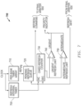
- FIG. 7 illustrates a block diagram of a refresh logic circuit 700 that may be used for refresh logic circuit 532 of FIGs. 5 and 6 according to some embodiments.
- Refresh logic circuit 700 includes generally a refresh internal timer 705, a per-bank timer array 710, a pending refresh queue 720, an owed refresh counter 730, a first comparator 740, and a second comparator 750.
- Refresh internal timer 705 has an input connected to a clock source and an output for providing an incremental count to owed refresh counter 730.
- Per-bank timer array 710 has an input for receiving a clock signal, and an output for providing a per-bank refresh to pending refresh queue 720.
- Pending refresh queue 720 has a first input connected to per-bank timer array 710, a second input, and an output for providing the refresh command to final arbiter 650.
- Owed refresh counter 730 has a first input labeled "INC”, a second input labeled "DEC" connected to the output of final arbiter 650, and an output. The output of owed refresh counter 730 provides an owed refresh count to first comparator 740 and second comparator 750.
- First comparator 740 also includes a second input for receiving a programmable urgent refresh limit, and an output for providing a priority indicator to the refresh command.
- Second comparator 750 also includes a second input for receiving a programmable intermediate refresh limit, and an output labeled "URGENT" for providing a priority indicator to final arbiter 650 with the refresh command signal.
- Final arbiter 650 provides a "refresh sent" signal to pending refresh queue 720 and owed refresh counter 730 to track the number of pending refreshes.
- refresh logic circuit 700 receives a clock signal for tracking tREFI.
- Refresh logic circuit 700 determines the intermediate refresh time interval based on tREFI and provides a refresh command based on the clock signal and the total number of banks assigned to the memory controller.
- Each cycle an intermediate time period elapses without a refresh sent, refresh timer interval timer 705 signals to increment owed refresh counter 730.
- Per-bank timer array 710 receives the clock signal and provides a refresh command to pending refresh queue 720 that corresponds to a respective memory bank.
- Pending refresh queue 720 provides the refresh command and priority indicator to final arbiter 650.
- Refresh logic circuit 700 sets the value of the priority indicator according to a number of pending refreshes.
- First comparator 740 compares the number of owed refreshes to the urgent refresh limit and elevates the priority indicator for a pending refresh command when owed refresh counter 730 is above the urgent refresh limit.
- Second comparator 750 compares the number of owed refreshes to the intermediate refresh limit and sets the priority indicator to a first priority status when owed refresh counter 730 is above an intermediate refresh count threshold.
- refresh logic circuit 700 generates per two bank refresh commands.
- Refresh logic circuit 700 elevates a priority indicator for a pending refresh command for the paired bank when the priority indicator is a first priority status and a refresh timer is above a refresh timing interval. Accordingly, when one of the paired banks are page closed and the intermediate refresh interval has elapsed, the priority indicator is elevated to urgent refresh status for both paired banks.
- final arbiter 650 precharges both banks.
- refresh logic circuit 700 allows arbiter 538 to send most refreshes in time to avoid latency penalties due to urgent refreshes. Further, memory bandwidth is increased thereby enabling improved processor performance. In one example memory bandwidth utilization is increased by approximately 3% for double data rate type six synchronous graphics random-access memory (GDDR6) when intermediate refresh per bank is used in comparison to when only a casual or urgent refresh per bank scheme is utilized.
- GDDR6 synchronous graphics random-access memory
- the circuits of FIGs. 5 , 6 , and 7 may be implemented with various combinations of hardware and software.
- the hardware circuitry may include priority encoders, finite state machines, programmable logic arrays (PLAs), and the like, arbiter 538 could be implemented with a microcontroller executing stored program instructions to evaluate the relative timing eligibility of the pending commands.
- some of the instructions may be stored in a non-transitory computer memory or computer readable storage medium for execution by the microcontroller.
- the non-transitory computer readable storage medium includes a magnetic or optical disk storage device, solid-state storage devices such as Flash memory, or other non-volatile memory device or devices.
- the computer readable instructions stored on the non-transitory computer readable storage medium may be in source code, assembly language code, object code, or other instruction format that is interpreted and/or executable by one or more processors.
- APU 110 of FIG. 1 or memory controller 500 of FIG. 5 or any portions thereof, such as arbiter 538, may be described or represented by a computer accessible data structure in the form of a database or other data structure which can be read by a program and used, directly or indirectly, to fabricate integrated circuits.
- this data structure may be a behavioral-level description or register-transfer level (RTL) description of the hardware functionality in a high level design language (HDL) such as Verilog or VHDL.
- HDL high level design language
- the description may be read by a synthesis tool which may synthesize the description to produce a netlist comprising a list of gates from a synthesis library.
- the netlist includes a set of gates that also represent the functionality of the hardware comprising integrated circuits.
- the netlist may then be placed and routed to produce a data set describing geometric shapes to be applied to masks.
- the masks may then be used in various semiconductor fabrication steps to produce the integrated circuits.
- the database on the computer accessible storage medium may be the netlist (with or without the synthesis library) or the data set, as desired, or Graphic Data System (GDS) II data.
- GDS Graphic Data System
- Memory controller 500 and/or arbiter 538 may vary in different embodiments.
- Memory controller 500 may interface to other types of memory besides DDRx memory, such as high bandwidth memory (HBM), RAMbus DRAM (RDRAM), synchronous graphics random access memory and the like.
- HBM high bandwidth memory
- RDRAM RAMbus DRAM
- synchronous graphics random access memory and the like.
- HBM high bandwidth memory
- RDRAM RAMbus DRAM
- synchronous graphics random access memory synchronous graphics random access memory and the like.
- the illustrated embodiment showed each bank of memory corresponding to intermediate refresh per bank time intervals, in other embodiments both banks of a paired bank of memory can support responding to an intermediate refresh per bank time interval.
Landscapes
- Engineering & Computer Science (AREA)
- Theoretical Computer Science (AREA)
- Microelectronics & Electronic Packaging (AREA)
- Computer Hardware Design (AREA)
- Physics & Mathematics (AREA)
- General Engineering & Computer Science (AREA)
- General Physics & Mathematics (AREA)
- Human Computer Interaction (AREA)
- Dram (AREA)
- Memory System (AREA)
Description
- Computer systems typically use inexpensive and high density dynamic random-access memory (DRAM) chips for main memory. Most DRAM chips sold today are compatible with various double data rate (DDR) DRAM standards promulgated by the Joint Electron Devices Engineering Council (JEDEC). DRAM chips are not persistent memory devices. Therefore, periodic memory refresh is needed by the DRAM chips for data retention during normal operation of the computer system. Memory refresh is a background maintenance process required during operation of semiconductor DRAM. Each bit of memory data is stored as the presence or absence of an electric charge on small capacitors which form the DRAM chips. Charges on the capacitors leak away over time, and without a memory refresh, stored data will be lost. To prevent data loss, external circuitry sends commands to cause the memory to periodically read a row and rewrite the row, restoring the charges on the capacitors of the memory cells of the row to the original charge level. While refresh is occurring, the memory is not available for normal read and write operations.
- Attempts have been made to mediate the effects of refresh operations on DRAM bandwidth. Known memory controllers adopt one of two processes for refreshing DRAM. In a first example the memory controller waits until no other accesses to the memory are pending, then the memory controller provides a refresh to the memory. These are called casual refreshes. In another example, when the memory controller has waited too long, and the memory is in critical need of a refresh, and the memory controller provides urgent refreshes. Each of the foregoing examples may result in memory transactions being stalled, consequently producing a penalty in memory performance.
-
US 2018/018133 discloses a data processing system with a memory controller having a refresh logic circuit that generates refresh requests separate from normal read and write memory access requests, and an arbiter that arbitrates between normal read and write memory access requests stored in a command queue and the refresh requests generated by the refresh logic circuit.US 2018/018291 A1 discloses a memory controller having three sub-arbiters for different types of page statuses, and a final arbiter that selects between three sub-arbitration winners as well as a refresh operation from refresh logic that generates autorefresh commands periodically. - The invention provides a memory controller in accordance with claim 1, a data processing system in accordance with claim 8, and a method for managing refresh of a memory in a memory system in accordance with claim 9.
-
-
FIG. 1 illustrates in block diagram form a data processing system according to some embodiments; -
FIG. 2 illustrates in block diagram form an accelerated processing unit (APU) suitable for use in the data processing system ofFIG. 1 ; -
FIG. 3 illustrates in block diagram form a memory controller and associated physical interface (PHY) suitable for use in the APU ofFIG. 2 according to some embodiments; -
FIG. 4 illustrates in block diagram form another memory controller and associated PHY suitable for use in the APU ofFIG. 2 according to some embodiments; -
FIG. 5 illustrates in block diagram form a memory controller according to some embodiments; -
FIG. 6 illustrates a block diagram of a portion of memory controller according to some embodiments; and -
FIG. 7 illustrates a block diagram of a refresh logic circuit that may be used for the refresh logic circuit ofFIGs. 5 and6 according to some embodiments. - In the following description, the use of the same reference numerals in different drawings indicates similar or identical items. Unless otherwise noted, the word "coupled" and its associated verb forms include both direct connection and indirect electrical connection by means known in the art, and unless otherwise noted any description of direct connection implies alternate embodiments using suitable forms of indirect electrical connection as well.
- As will be described below in one form, a memory controller includes a command queue, an arbiter, a refresh logic circuit, and a final arbiter. The command queue receives and stores memory access requests for a memory. The arbiter selectively picks accesses from the command queue according to a first type of accesses and a second type of accesses. The first type of accesses and the second type of accesses correspond to different page statuses of corresponding memory accesses in the memory. The refresh logic circuit generates a refresh command to a bank of the memory. The refresh logic circuit provides a priority indicator with the refresh command whose value is set according to a number of pending refreshes. The final arbiter selectively orders the refresh command with respect to memory access requests of the first type accesses and the second type accesses. The ordering is based on the priority indicator.
- In another form, a data processing system includes a memory accessing agent, a memory system, and a memory controller. The memory accessing agent provides memory access requests for a memory. The memory system is coupled to the memory accessing agent. The memory controller is coupled to the memory system and the memory accessing agent includes a command queue, an arbiter, and a final arbiter. The command queue stores memory access commands received from the memory accessing agent. The arbiter selectively picks memory accesses from the command queue according to a first type of access and a second type of access. Each type of access corresponds to a different page status of a bank in the memory. The final arbiter arbitrates based on input received from a refresh logic circuit. The refresh logic circuit generates a refresh command to the bank of the memory and provides a priority indicator to the refresh command. The value of the priority indicator is set according to a number of pending refreshes, to selectively order the refresh command with respect to a first type of access and a second type of access.
- In yet another form, a method for managing refresh of a memory in a memory system via a memory controller. A plurality of memory access requests is received and stored in a command queue. The memory accesses requests are selectively picked from the command queue according to a first type of accesses and a second type of accesses. The first type of accesses and a second type of accesses correspond to different page statuses of corresponding memory accesses in the memory. A refresh command is generated to a bank of the memory. A priority indicator is provided with the refresh command. The refresh command is selectively ordered with respect to memory access requests of the first type access and the second type access based on the priority indicator.
-
FIG. 1 illustrates in block diagram form adata processing system 100 according to some embodiments.Data processing system 100 includes generally adata processor 110 in the form of an accelerated processing unit (APU), amemory system 120, a peripheral component interconnect express (PCIe)system 150, a universal serial bus (USB)system 160, and adisk drive 170.Data processor 110 operates as the central processing unit (CPU) ofdata processing system 100 and provides various buses and interfaces useful in modern computer systems. These interfaces include two double data rate (DDRx) memory channels, a PCIe root complex for connection to a PCIe link, a USB controller for connection to a USB network, and an interface to a Serial Advanced Technology Attachment (SATA) mass storage device. -
Memory system 120 includes amemory channel 130 and amemory channel 140.Memory channel 130 includes a set of dual inline memory modules (DIMMs) connected to aDDRx bus 132, includingrepresentative DIMMs memory channel 140 includes a set of DIMMs connected to aDDRx bus 142, includingrepresentative DIMMs -
PCIe system 150 includes aPCIe switch 152 connected to the PCIe root complex indata processor 110, aPCIe device 154, aPCIe device 156, and aPCIe device 158.PCIe device 156 in turn is connected to a system basic input/output system (BIOS)memory 157.System BIOS memory 157 can be any of a variety of non-volatile memory types, such as read-only memory (ROM), flash electrically erasable programmable ROM (EEPROM), and the like. -
USB system 160 includes aUSB hub 162 connected to a USB master indata processor 110, andrepresentative USB devices USB hub 162.USB devices -
Disk drive 170 is connected todata processor 110 over a SATA bus and provides mass storage for the operating system, application programs, application files, and the like. -
Data processing system 100 is suitable for use in modem computing applications by providing amemory channel 130 and amemory channel 140. Each ofmemory channels -
FIG. 2 illustrates in block diagram form anAPU 200 suitable for use indata processing system 100 ofFIG. 1 .APU 200 includes generally a central processing unit (CPU)core complex 210, agraphics core 220, a set ofdisplay engines 230, amemory management hub 240, adata fabric 250, a set ofperipheral controllers 260, a set ofperipheral bus controllers 270, a system management unit (SMU) 280, and a set ofmemory controllers 290. -
CPU core complex 210 includes aCPU core 212 and aCPU core 214. In this example,CPU core complex 210 includes two CPU cores, but in other embodimentsCPU core complex 210 can include an arbitrary number of CPU cores. Each ofCPU cores data fabric 250, and is capable of providing memory access requests todata fabric 250. Each ofCPU cores -
Graphics core 220 is a high performance graphics processing unit (GPU) capable of performing graphics operations such as vertex processing, fragment processing, shading, texture blending, and the like in a highly integrated and parallel fashion.Graphics core 220 is bidirectionally connected to the SMN and todata fabric 250, and is capable of providing memory access requests todata fabric 250. In this regard,APU 200 may either support a unified memory architecture in whichCPU core complex 210 andgraphics core 220 share the same memory space, or a memory architecture in whichCPU core complex 210 andgraphics core 220 share a portion of the memory space, whilegraphics core 220 also uses a private graphics memory not accessible byCPU core complex 210. -
Display engines 230 render and rasterize objects generated bygraphics core 220 for display on a monitor.Graphics core 220 anddisplay engines 230 are bidirectionally connected to a commonmemory management hub 240 for uniform translation into appropriate addresses inmemory system 120, andmemory management hub 240 is bidirectionally connected todata fabric 250 for generating such memory accesses and receiving read data returned from the memory system. -
Data fabric 250 includes a crossbar switch for routing memory access requests and memory responses between any memory accessing agent andmemory controllers 290. It also includes a system memory map, defined by BIOS, for determining destinations of memory accesses based on the system configuration, as well as buffers for each virtual connection. -
Peripheral controllers 260 include aUSB controller 262 and a SATA interface controller 264, each of which is bidirectionally connected to asystem hub 266 and to the SMN bus. These two controllers are merely exemplary of peripheral controllers that may be used inAPU 200. -
Peripheral bus controllers 270 include a system controller or "Southbridge" (SB) 272 and aPCIe controller 274, each of which is bidirectionally connected to an input/output (I/O)hub 276 and to the SMN bus. I/O hub 276 is also bidirectionally connected tosystem hub 266 and todata fabric 250. Thus, for example a CPU core can program registers inUSB controller 262, SATA interface controller 264,SB 272, orPCIe controller 274 through accesses thatdata fabric 250 routes through I/O hub 276. -
SMU 280 is a local controller that controls the operation of the resources onAPU 200 and synchronizes communication among them.SMU 280 manages power-up sequencing of the various processors onAPU 200 and controls multiple off-chip devices via reset, enable and other signals.SMU 280 includes one or more clock sources not shown inFIG. 2 , such as a phase locked loop (PLL), to provide clock signals for each of the components ofAPU 200.SMU 280 also manages power for the various processors and other functional blocks, and may receive measured power consumption values fromCPU cores graphics core 220 to determine appropriate power states. -
APU 200 also implements various system monitoring and power saving functions. In particular one system monitoring function is thermal monitoring. For example, ifAPU 200 becomes hot, thenSMU 280 can reduce the frequency and voltage ofCPU cores graphics core 220. IfAPU 200 becomes too hot, then it can be shut down entirely. Thermal events can also be received from external sensors bySMU 280 via the SMN bus, andSMU 280 can reduce the clock frequency and/or power supply voltage in response. -
FIG. 3 illustrates in block diagram form amemory controller 300 and an associated physical interface (PHY) 330 suitable for use inAPU 200 ofFIG. 2 according to some embodiments.Memory controller 300 includes a memory channel 310 and apower engine 320. Memory channel 310 includes ahost interface 312, amemory channel controller 314, and aphysical interface 316.Host interface 312 bidirectionally connectsmemory channel controller 314 todata fabric 250 over a scalable data port (SDP).Physical interface 316 bidirectionally connectsmemory channel controller 314 toPHY 330 over a bus that conforms to the DDR-PHY Interface Specification (DFI).Power engine 320 is bidirectionally connected toSMU 280 over the SMN bus, to PHY 330 over the Advanced Peripheral Bus (APB), and is also bidirectionally connected tomemory channel controller 314.PHY 330 has a bidirectional connection to a memory channel such asmemory channel 130 ormemory channel 140 ofFIG. 1 .Memory controller 300 is an instantiation of a memory controller for a single memory channel using a singlememory channel controller 314, and has apower engine 320 to control operation ofmemory channel controller 314 in a manner that will be described further below. -
FIG. 4 illustrates in block diagram form anothermemory controller 400 and associatedPHYs APU 200 ofFIG. 2 according to some embodiments.Memory controller 400 includesmemory channels 410 and 420 and apower engine 430.Memory channel 410 includes ahost interface 412, amemory channel controller 414, and aphysical interface 416.Host interface 412 bidirectionally connectsmemory channel controller 414 todata fabric 250 over an SDP.Physical interface 416 bidirectionally connectsmemory channel controller 414 toPHY 440, and conforms to the DFI Specification. Memory channel 420 includes a host interface 422, amemory channel controller 424, and aphysical interface 426. Host interface 422 bidirectionally connectsmemory channel controller 424 todata fabric 250 over another SDP.Physical interface 426 bidirectionally connectsmemory channel controller 424 toPHY 450, and conforms to the DFISpecification. Power engine 430 is bidirectionally connected toSMU 280 over the SMN bus, to PHYs 440 and 450 over the APB, and is also bidirectionally connected tomemory channel controllers PHY 440 has a bidirectional connection to a memory channel such asmemory channel 130 ofFIG. 1 .PHY 450 has a bidirectional connection to a memory channel such asmemory channel 140 ofFIG. 1 .Memory controller 400 is an instantiation of a memory controller having two memory channel controllers and uses a sharedpower engine 430 to control operation of bothmemory channel controller 414 andmemory channel controller 424 in a manner that will be described further below. -
FIG. 5 illustrates in block diagram form amemory controller 500 according to some embodiments.Memory controller 500 includes amemory channel controller 510 and apower controller 550.Memory channel controller 510 includes aninterface 512, aqueue 514, acommand queue 520, anaddress generator 522, a content addressable memory (CAM) 524, areplay queue 530, a refreshlogic circuit block 532, atiming block 534, a page table 536, anarbiter 538, an error correction code (ECC)check block 542, anECC generation block 544, and a data buffer (DB) 546. -
Interface 512 has a first bidirectional connection todata fabric 250 over an external bus, and has an output. Inmemory controller 500, this external bus is compatible with the advanced extensible interface version four specified by ARM Holdings, PLC of Cambridge, England, known as "AXI4", but can be other types of interfaces in other embodiments.Interface 512 translates memory access requests from a first clock domain known as the FCLK (or MEMCLK) domain to a second clock domain internal tomemory controller 500 known as the UCLK domain. Similarly,queue 514 provides memory accesses from the UCLK domain to the DFICLK domain associated with the DFI interface. -
Address generator 522 decodes addresses of memory access requests received fromdata fabric 250 over the AXI4 bus. The memory access requests include access addresses in the physical address space represented as a normalized address.Address generator 522 converts the normalized addresses into a format that can be used to address the actual memory devices inmemory system 120, as well as to efficiently schedule related accesses. This format includes a region identifier that associates the memory access request with a particular rank, a row address, a column address, a bank address, and a bank group. On startup, the system BIOS queries the memory devices inmemory system 120 to determine their size and configuration, and programs a set of configuration registers associated withaddress generator 522.Address generator 522 uses the configuration stored in the configuration registers to translate the normalized addresses into the appropriate format.Command queue 520 is a queue of memory access requests received from the memory accessing agents indata processing system 100, such asCPU cores graphics core 220.Command queue 520 stores the address fields decoded byaddress generator 522 as well other address information that allowsarbiter 538 to select memory accesses efficiently, including access type and quality of service (QoS) identifiers.CAM 524 includes information to enforce ordering rules, such as write after write (WAW) and read after write (RAW) ordering rules. -
Replay queue 530 is a temporary queue for storing memory accesses picked byarbiter 538 that are awaiting responses, such as address and command parity responses, write cyclic redundancy check (CRC) responses for DDR4 DRAM or write and read CRC responses for GDDR5 DRAM.Replay queue 530 accessesECC check block 542 to determine whether the returned ECC is correct or indicates an error.Replay queue 530 allows the accesses to be replayed in the case of a parity or CRC error of one of these cycles. -
Refresh logic circuit 532 includes state machines for various powerdown, refresh, and termination resistance (ZQ) calibration cycles that are generated separately from normal read and write memory access requests received from memory accessing agents. For example, if a memory rank is in precharge powerdown, it must be periodically awakened to run refresh cycles.Refresh logic circuit 532 generates auto-refresh commands periodically to prevent data errors caused by leaking of charge off storage capacitors of memory cells in DRAM chips. In addition,refresh logic circuit 532 periodically calibrates ZQ to prevent mismatch in on-die termination resistance due to thermal changes in the system.Refresh logic circuit 532 also decides when to put DRAM devices in different power down modes. -
Arbiter 538 is bidirectionally connected tocommand queue 520 and is the heart ofmemory channel controller 510. It improves efficiency by intelligent scheduling of accesses to improve the usage of the memory bus.Arbiter 538 usestiming block 534 to enforce proper timing relationships by determining whether certain accesses incommand queue 520 are eligible for issuance based on DRAM timing parameters. For example, each DRAM has a minimum specified time between activate commands to the same bank, known as "tRC".Timing block 534 maintains a set of counters that determine eligibility based on this and other timing parameters specified in the JEDEC specification, and is bidirectionally connected to replayqueue 530. Page table 536 maintains state information about active pages in each bank and rank of the memory channel forarbiter 538, and is bidirectionally connected to replayqueue 530. - In response to write memory access requests received from
interface 512,ECC generation block 544 computes an ECC according to the write data.DB 546 stores the write data and ECC for received memory access requests. It outputs the combined write data/ECC to queue 514 whenarbiter 538 picks the corresponding write access for dispatch to the memory channel. -
Power controller 550 includes aninterface 552 to an advanced extensible interface, version one (AXI), anAPB interface 554, and apower engine 560.Interface 552 has a first bidirectional connection to the SMN, which includes an input for receiving an event signal labeled "EVENT_n" shown separately inFIG. 5 , and an output.APB interface 554 has an input connected to the output ofinterface 552, and an output for connection to a PHY over anAPB. Power engine 560 has an input connected to the output ofinterface 552, and an output connected to an input ofqueue 514.Power engine 560 includes a set of configuration registers 562, a microcontroller (µC) 564, a self refresh controller (SLFREF/PE) 566, and a reliable read/write training engine (RRW/TE) 568. Configuration registers 562 are programmed over the AXI bus, and store configuration information to control the operation of various blocks inmemory controller 500. Accordingly, configuration registers 562 have outputs connected to these blocks that are not shown in detail inFIG. 5 .Self refresh controller 566 is an engine that allows the manual generation of refreshes in addition to the automatic generation of refreshes byrefresh logic circuit 532. Reliable read/write training engine 568 provides a continuous memory access stream to memory or I/O devices for such purposes as DDR interface read latency training and loopback testing. -
Memory channel controller 510 includes circuitry that allows it to pick memory accesses for dispatch to the associated memory channel. In order to make the desired arbitration decisions,address generator 522 decodes the address information into predecoded information including rank, row address, column address, bank address, and bank group in the memory system, andcommand queue 520 stores the predecoded information. Configuration registers 562 store configuration information to determine howaddress generator 522 decodes the received address information.Arbiter 538 uses the decoded address information, timing eligibility information indicated by timingblock 534, and active page information indicated by page table 536 to efficiently schedule memory accesses while observing other criteria such as QoS requirements. For example,arbiter 538 implements a preference for accesses to open pages to avoid the overhead of precharge and activation commands required to change memory pages, and hides overhead accesses to one bank by interleaving them with read and write accesses to another bank. In particular during normal operation,arbiter 538 may decide to keeps pages open in different banks until they are required to be precharged prior to selecting a different page. -
FIG. 6 illustrates a block diagram of aportion 600 ofmemory controller 500 ofFIG. 5 according to some embodiments.Portion 600 includesarbiter 538, refreshlogic circuit 532, and a set ofcontrol circuits 660 associated with the operation ofarbiter 538.Arbiter 538 includes a set ofsub-arbiters 605 and afinal arbiter 650.Sub-arbiters 605 include a sub-arbiter 610, a sub-arbiter 620, and a sub-arbiter 630.Sub-arbiter 610 includes a page hitarbiter 612 labeled "PH ARB", and anoutput register 614. Page hitarbiter 612 has a first input connected tocommand queue 520, a second input, and an output.Register 614 has a data input connected to the output of page hitarbiter 612, a clock input for receiving the UCLK signal, and an output.Sub-arbiter 620 includes apage conflict arbiter 622 labeled "PC ARB", and anoutput register 624.Page conflict arbiter 622 has a first input connected tocommand queue 520, a second input, and an output.Register 624 has a data input connected to the output ofpage conflict arbiter 622, a clock input for receiving the UCLK signal, and an output.Sub-arbiter 630 includes apage miss arbiter 632 labeled "PM ARB", and anoutput register 634.Page miss arbiter 632 has a first input connected tocommand queue 520, a second input, and an output.Register 634 has a data input connected to the output ofpage miss arbiter 632, a clock input for receiving the UCLK signal, and an output.Final arbiter 650 has a first input connected to the output of pageclose predictor 662, a second input connected to the output ofrefresh logic circuit 532, a third input connected to the output ofoutput register 614, a fourth input connected to the output ofoutput register 624, a fifth input connected to the output ofregister 634, and a first output for providing an arbitration winner to queue 514. - The output of
refresh logic circuit 532 provides a priority indicator with an associated refresh command.Refresh logic circuit 532 also has an input connected to the output offinal arbiter 650. -
Control circuits 660 include timingblock 534 and page table 536 as previously described with respect toFIG. 5 , and a pageclose predictor 662.Timing block 534 has an input and an output connected to the first inputs of page hitarbiter 612,page conflict arbiter 622, and page missarbiter 632. Page table 536 has an input connected to an output ofreplay queue 530, an output connected to an input ofreplay queue 530, an output connected to the input ofcommand queue 520, an output connected to the input oftiming block 534, and an output connected to the input of pageclose predictor 662. Pageclose predictor 662 has an input connected to one output of page table 536, an input connected to the output ofoutput register 614, and an output connected to the second input offinal arbiter 650. - In operation,
arbiter 538 selects memory access requests (commands) fromcommand queue 520 and refreshlogic 532 by taking into account the page status of each entry and the priority of each refresh command. The memory access priority is based on the intermediate refresh interval, but can be altered based on the page status of the memory access request and on a priority indicator status of the refresh command.Arbiter 538 includes three sub-arbiters that operate in parallel withrefresh logic circuit 532 to address the mismatch between the processing and transmission limits of existing integrated circuit technology. The winners of the respective sub-arbitrations are presented tofinal arbiter 650 along with a refresh command having a priority indicator.Final arbiter 650 selects between these three sub-arbitration winners and a refresh operation fromrefresh logic 532 to output to queue 514. - Each of page hit
arbiter 612,page conflict arbiter 622, and page missarbiter 632 has an input connected to the output oftiming block 534 to determine timing eligibility of commands incommand queue 520 that fall into these respective categories.Timing block 534 includes an array of binary counters that count durations related to the particular operations for each bank in each rank. The number of timers needed to determine the status depends on the timing parameter, the number of banks for the given memory type, and the number of ranks supported by the system on a given memory channel. The number of timing parameters that are implemented in turn depends on the type of memory implemented in the system. For example, GDDR5 memories require more timers to comply with more timing parameters than other DDRx memory types. By including an array of generic timers implemented as binary counters, timing block 534 can be scaled and reused for different memory types. - A page hit is a read or write cycle to an open page. Page hit
arbiter 612 arbitrates between accesses incommand queue 520 to open pages. A page conflict is an access to one row in a bank when another row in the bank is currently activated.Page conflict arbiter 622 arbitrates between accesses incommand queue 520 to pages that conflict with the page that is currently open in the corresponding bank and rank.Page conflict arbiter 622 selects a sub-arbitration winner that causes the issuance of a precharge command. A page miss is an access to a bank that is in the precharged state.Page miss arbiter 632 arbitrates between accesses incommand queue 520 to precharged memory banks.Arbiter 538 selectively picks accesses fromcommand queue 520 according to the type of memory access. Each of page hitarbiter 612,page conflict arbiter 622, and page missarbiter 632 outputs a first type of accesses or a second type of accesses. - The first type of accesses and the second type of accesses correspond to different page statuses of corresponding memory accesses in the memory. More specifically, page hit
arbiter 612 outputs a first type access.Page conflict arbiter 622 and page missarbiter 632 each output a second type access. After determining the relative priority among the three sub-arbitration winners,final arbiter 650 then determines whether the sub-arbitration winners conflict with the refresh command (i.e. whether they are directed to the same bank and rank). When there are no such conflicts and the refresh time interval is met, thenfinal arbiter 650 selects the refresh command. When there are conflicts, thenfinal arbiter 650 complies with the following rules. When the priority indicator for the refresh command is a first priority status (intermediate priority) and page hitarbiter 612 selects a pending page hit, thenfinal arbiter 650 selects the access indicated by page hitarbiter 612. When the priority indicator for the refresh command is a second priority status (urgent priority) and the sub-arbitration winner is from page hitarbiter 612,final arbiter 650 selects the access indicated byrefresh logic circuit 532, thereby prioritizing the refresh command to execute instead of the page hit. In some cases refreshlogic circuit 532 elevates the priority status of the refresh command to an urgent status, based on an urgent refresh count threshold. -
Refresh logic circuit 532 provides a priority indicator with the refresh command to specify a priority status of the refresh command tofinal arbiter 650.Refresh logic circuit 532 sets the value of the priority indicator according to a number of pending refreshes.Refresh logic circuit 532 assigns to the priority indicator a first priority status or a second priority status.Refresh logic 532 evenly spreads out a per bank refresh cycle based on a predetermined time period. The predetermined time period is an intermediate refresh interval that is a timing dependent refresh interval, that is based on refresh time interval (tREFI) and the number of memory banks that are assigned to the memory controller. The trigger of the intermediate refresh is dependent on a threshold of owed refreshes. - Within
refresh logic circuit 532, priority is initially set based on the number of pending refreshes. In general, refreshlogic circuit 532 elevates the refresh command to execute between the first type of accesses and the second type of accesses. More specifically,final arbiter 650 sends the refresh command when there is no page hit transaction to the target memory banks. In response to the second priority status,final arbiter 650 elevates the refresh command above the first type of accesses and the second type of accesses. Thereby, in some cases,final arbiter 650 prioritizes the refresh command to execute instead of pending requests to the memory bank. - By using sub-arbiters for page hits, page conflicts, and page misses,
arbiter 538 can selectively pick accesses based on sub-arbitrations, and categorize them as a first type of access and a second type of access.Final arbiter 650 can select refresh commands based on input received fromrefresh logic circuit 532 which generates the refresh command tobank 134 ofmemory 132 based on the number of pending refreshes.Final arbiter 650 orders the refresh command with respect to a first type of access and a second type of access. The intermediate refresh time interval is a time period that is less than tREFI. Ordering the refresh commands based on the types of memory accesses and according to the number of pending refreshes allows refresh commands to be sent at a higher frequency than the refresh time interval and in a sufficient amount of time to avoid penalties due to urgent refreshes. - In other embodiments,
arbiter 538 could include a different number of sub-arbiters. For example,arbiter 538 could include two sub-arbiters, one arbiter for page hits and another arbiter for page conflicts and page misses. In this case,arbiter 538 is able to access page types based on the two sub-arbitrations. - In some embodiments, refresh
logic circuit 532 generates the refresh command per bank in one tREFI so that during high workloads when some banks are refreshing, other transactions are utilizing other banks withmemory 132 to more fully take advantage of bus bandwidth ofmemory 132. In general, to send out the intermediate refresh command during transactionsfinal arbiter 650 asserts an urgent refresh status to the intermediate refresh command having a first or second priority status when a predetermined clock cycle expires and the page of the bank is closed. This allows the intermediate refresh per bank command to be generated tomemory 132 evenly and consistently.Final arbiter 650 arbitrates an intermediate refresh per bank command to generate to the bank between page hits and page misses. Elevating the priority of the intermediate refresh per bank command to generate between page hits and page misses further savesmemory 132 from penalties that derive from closing the pages. Advantageously, intermediate refresh per bank command alleviates the clock cycles required between opening a row of memory and accessing columns within the row (trcd), and alleviates the clock cycles required between issuing the precharge command and opening the next row (trp). - In some embodiments, the
arbiter 538 relegates the priority of the memory banks using a priority indicator. In response to simultaneously receiving a refresh command to at least two memory banks with an equivalent priority indicator,arbiter 538 relegates the memory bank that is a most recent recipient of the refresh command below the bank of memory that is the least recent recipient of the refresh command. In response to receiving an urgent refresh command fromrefresh logic circuit 532,arbiter 538 blocks the activation of a row of the corresponding bank so that no new activity is started in the bank. After receiving an urgent refresh command for the bank,arbiter 538 sends the refresh request to the bank in two conditions. First,arbiter 538 sends the urgent refresh command to the bank right away if the refresh timing was met at the same time as the urgent refresh command was generated. Second, if the refresh timing was not met at the same time that the urgent refresh command was generated,arbiter 538 waits for the refresh timing to be met, and then sends a refresh request to the corresponding bank. -
FIG. 7 illustrates a block diagram of arefresh logic circuit 700 that may be used forrefresh logic circuit 532 ofFIGs. 5 and6 according to some embodiments.Refresh logic circuit 700 includes generally a refreshinternal timer 705, a per-bank timer array 710, a pendingrefresh queue 720, an owedrefresh counter 730, afirst comparator 740, and asecond comparator 750. - Refresh
internal timer 705 has an input connected to a clock source and an output for providing an incremental count to owedrefresh counter 730. Per-bank timer array 710 has an input for receiving a clock signal, and an output for providing a per-bank refresh to pendingrefresh queue 720.Pending refresh queue 720 has a first input connected to per-bank timer array 710, a second input, and an output for providing the refresh command tofinal arbiter 650. Owedrefresh counter 730 has a first input labeled "INC", a second input labeled "DEC" connected to the output offinal arbiter 650, and an output. The output of owedrefresh counter 730 provides an owed refresh count tofirst comparator 740 andsecond comparator 750.First comparator 740 also includes a second input for receiving a programmable urgent refresh limit, and an output for providing a priority indicator to the refresh command.Second comparator 750 also includes a second input for receiving a programmable intermediate refresh limit, and an output labeled "URGENT" for providing a priority indicator tofinal arbiter 650 with the refresh command signal.Final arbiter 650 provides a "refresh sent" signal to pendingrefresh queue 720 and owedrefresh counter 730 to track the number of pending refreshes. - In operation, refresh
logic circuit 700 receives a clock signal for tracking tREFI.Refresh logic circuit 700 determines the intermediate refresh time interval based on tREFI and provides a refresh command based on the clock signal and the total number of banks assigned to the memory controller. Each cycle an intermediate time period elapses without a refresh sent, refreshtimer interval timer 705 signals to increment owedrefresh counter 730. Per-bank timer array 710 receives the clock signal and provides a refresh command to pendingrefresh queue 720 that corresponds to a respective memory bank.Pending refresh queue 720 provides the refresh command and priority indicator tofinal arbiter 650.Refresh logic circuit 700 sets the value of the priority indicator according to a number of pending refreshes.First comparator 740 compares the number of owed refreshes to the urgent refresh limit and elevates the priority indicator for a pending refresh command when owedrefresh counter 730 is above the urgent refresh limit.Second comparator 750 compares the number of owed refreshes to the intermediate refresh limit and sets the priority indicator to a first priority status when owedrefresh counter 730 is above an intermediate refresh count threshold. - In some embodiments, refresh
logic circuit 700 generates per two bank refresh commands.Refresh logic circuit 700 elevates a priority indicator for a pending refresh command for the paired bank when the priority indicator is a first priority status and a refresh timer is above a refresh timing interval. Accordingly, when one of the paired banks are page closed and the intermediate refresh interval has elapsed, the priority indicator is elevated to urgent refresh status for both paired banks. In response to pages being open in the target banks,final arbiter 650 precharges both banks. - By selecting indicating intermediate priority for per-bank refresh commands, refresh
logic circuit 700 allowsarbiter 538 to send most refreshes in time to avoid latency penalties due to urgent refreshes. Further, memory bandwidth is increased thereby enabling improved processor performance. In one example memory bandwidth utilization is increased by approximately 3% for double data rate type six synchronous graphics random-access memory (GDDR6) when intermediate refresh per bank is used in comparison to when only a casual or urgent refresh per bank scheme is utilized. - The circuits of
FIGs. 5 ,6 , and7 may be implemented with various combinations of hardware and software. For example, the hardware circuitry may include priority encoders, finite state machines, programmable logic arrays (PLAs), and the like,arbiter 538 could be implemented with a microcontroller executing stored program instructions to evaluate the relative timing eligibility of the pending commands. In this case some of the instructions may be stored in a non-transitory computer memory or computer readable storage medium for execution by the microcontroller. In various embodiments, the non-transitory computer readable storage medium includes a magnetic or optical disk storage device, solid-state storage devices such as Flash memory, or other non-volatile memory device or devices. The computer readable instructions stored on the non-transitory computer readable storage medium may be in source code, assembly language code, object code, or other instruction format that is interpreted and/or executable by one or more processors. -
APU 110 ofFIG. 1 ormemory controller 500 ofFIG. 5 or any portions thereof, such asarbiter 538, may be described or represented by a computer accessible data structure in the form of a database or other data structure which can be read by a program and used, directly or indirectly, to fabricate integrated circuits. For example, this data structure may be a behavioral-level description or register-transfer level (RTL) description of the hardware functionality in a high level design language (HDL) such as Verilog or VHDL. The description may be read by a synthesis tool which may synthesize the description to produce a netlist comprising a list of gates from a synthesis library. The netlist includes a set of gates that also represent the functionality of the hardware comprising integrated circuits. The netlist may then be placed and routed to produce a data set describing geometric shapes to be applied to masks. The masks may then be used in various semiconductor fabrication steps to produce the integrated circuits. Alternatively, the database on the computer accessible storage medium may be the netlist (with or without the synthesis library) or the data set, as desired, or Graphic Data System (GDS) II data. - While particular embodiments have been described, various modifications to these embodiments will be apparent to those skilled in the art. For example, the internal architecture of
memory controller 500 and/orarbiter 538 may vary in different embodiments.Memory controller 500 may interface to other types of memory besides DDRx memory, such as high bandwidth memory (HBM), RAMbus DRAM (RDRAM), synchronous graphics random access memory and the like. While the illustrated embodiment showed each bank of memory corresponding to intermediate refresh per bank time intervals, in other embodiments both banks of a paired bank of memory can support responding to an intermediate refresh per bank time interval.
Claims (15)
- A memory controller (500), comprising:a command queue (520) for receiving and storing memory access requests for a memory (120);an arbiter (605) for selectively picking accesses from the command queue (520) and categorizing them as a first type of accesses or a second type of accesses, wherein the first type of accesses and the second type of accesses correspond to different page statuses of corresponding memory accesses in the memory;a refresh logic circuit (532) for generating a refresh command to a bank of the memory (120), and providing a priority indicator with the refresh command whose value is set according to a number of pending per-bank refreshes, wherein the refresh logic circuit (532) assigns the priority indicator one of a first priority status and a second priority status; anda final arbiter (650) for selectively ordering the refresh command with respect to memory access requests of the first type accesses and the second type accesses based on the priority indicator, wherein the final arbiter prioritizes the refresh command to execute in an order between the first type of accesses and the second type of accesses when the priority indicator is the first priority status.
- The memory controller of claim 1, wherein the refresh logic circuit (532) further elevates the refresh command to execute in an order above the first type of accesses and the second type of accesses if the priority indicator for the refresh command is the second priority status.
- The memory controller of claim 1, wherein the refresh logic circuit (532) comprises:a refresh counter (720) that counts the number of pending per-bank refreshes; anda comparator (750) coupled to the refresh counter (720) that provides the first priority status to the refresh command if the refresh counter (720) exceeds a predetermined threshold.
- The memory controller of claim 3, wherein, based on a refresh interval, the refresh logic circuit (532) further elevates the priority indicator for a pending refresh command when the refresh counter (720) is between a lower limit and an upper limit.
- The memory controller of claim 1, wherein the refresh logic circuit (532) further assigns the priority indicator using an output of a programmable counter (730), and the programmable counter (730) tracks a number of pending refresh commands.
- The memory controller of claim 5, wherein the refresh logic circuit (532) further elevates the priority indicator for a pending refresh command when the programmable counter (730) is above an urgent refresh limit.
- The memory controller of claim 1, wherein in response to simultaneously receiving a priority indicator for more than one bank, the final arbiter (650) relegates the priority indicator of the bank of the memory (120) that is a most recent recipient of the refresh command below the bank of the memory (120) that is a least recent recipient of the refresh command.
- A data processing system, comprising:a memory accessing agent (210/220) for providing memory access requests for a memory;a memory system (120) coupled to the memory accessing agent (210/220); anda memory controller (500) as recited in any of claims 1-7.
- A method for managing refresh of a memory in a memory system (120) via a memory controller, the method comprising:receiving a plurality of memory access requests;storing the plurality of memory access requests in a command queue (520); andselectively picking memory accesses requests from the command queue (520) and categorizing them as a first type of accesses or a second type of accesses that correspond to different page statuses of corresponding memory accesses in the memory (120);generating a refresh command to a bank of the memory (120), and providing a priority indicator with the refresh command whose value is set according to a number of pending per-bank refreshes, wherein providing the priority indicator to the refresh command further comprises assigning the priority indicator one of a first priority status and a second priority status, and prioritizing the refresh command between the first type accesses and the second type accesses when the priority indicator is the first priority status; andselectively ordering the refresh command to execute in an order with respect to memory access requests of the first type of accesses and the second type of accesses based on the priority indicator.
- The method of claim 9, wherein providing the priority indicator to the refresh command further comprises:
elevating the refresh command to execute in an order above the first type accesses and the second type of accesses if the priority indicator for the refresh command is the second priority status. - The method of claim 9, further comprising assigning the priority indicator based on a predetermined threshold of a refresh counter (730), wherein the refresh counter (730) counts the number of pending per-bank refreshes in the memory (120).
- The method of claim 11, further comprising elevating the priority indicator for a pending refresh command, based on a refresh interval, when the refresh counter (730) is between a lower limit and an upper limit.
- The method of claim 9, further comprising assigning the priority indicator using an output of a programmable counter (730), and the programmable counter (730) tracks a number of refresh commands that are scheduled and incomplete.
- The method of claim 9, further comprising selectively picking accesses using sub-arbitrations, wherein an arbiter (500) comprises a plurality of sub-arbiters (610/620/630) and one sub-arbitration is a page hit and each other sub-arbitration is not a page hit.
- The method of claim 9, wherein the refresh command is for a selected bank.
Applications Claiming Priority (3)
| Application Number | Priority Date | Filing Date | Title |
|---|---|---|---|
| CN201810775044.XA CN110729006B (en) | 2018-07-16 | 2018-07-16 | Refresh Schemes in Memory Controllers |
| US16/038,738 US10593391B2 (en) | 2018-07-16 | 2018-07-18 | Refresh scheme in a memory controller |
| PCT/US2019/038541 WO2020018234A1 (en) | 2018-07-16 | 2019-06-21 | A refresh scheme in a memory controller |
Publications (3)
| Publication Number | Publication Date |
|---|---|
| EP3824466A1 EP3824466A1 (en) | 2021-05-26 |
| EP3824466A4 EP3824466A4 (en) | 2022-04-06 |
| EP3824466B1 true EP3824466B1 (en) | 2024-12-18 |
Family
ID=69139641
Family Applications (1)
| Application Number | Title | Priority Date | Filing Date |
|---|---|---|---|
| EP19837001.7A Active EP3824466B1 (en) | 2018-07-16 | 2019-06-21 | A refresh scheme in a memory controller |
Country Status (6)
| Country | Link |
|---|---|
| US (1) | US10593391B2 (en) |
| EP (1) | EP3824466B1 (en) |
| JP (1) | JP2022514128A (en) |
| KR (1) | KR102728014B1 (en) |
| CN (1) | CN110729006B (en) |
| WO (1) | WO2020018234A1 (en) |
Families Citing this family (26)
| Publication number | Priority date | Publication date | Assignee | Title |
|---|---|---|---|---|
| US8949520B2 (en) * | 2009-01-22 | 2015-02-03 | Rambus Inc. | Maintenance operations in a DRAM |
| US10475519B2 (en) | 2018-03-23 | 2019-11-12 | Micron Technology, Inc. | Methods for detecting and mitigating memory media degradation and memory devices employing the same |
| JP2020170315A (en) * | 2019-04-02 | 2020-10-15 | キヤノン株式会社 | Access control device |
| CN110265029A (en) * | 2019-06-21 | 2019-09-20 | 百度在线网络技术(北京)有限公司 | Speech chip and electronic equipment |
| KR102818463B1 (en) * | 2019-07-25 | 2025-06-10 | 삼성전자주식회사 | Master device and method of controlling the same |
| US11222685B2 (en) * | 2020-05-15 | 2022-01-11 | Advanced Micro Devices, Inc. | Refresh management for DRAM |
| US11561862B2 (en) | 2020-05-29 | 2023-01-24 | Advanced Micro Devices, Inc. | Refresh management for DRAM |
| US11809743B2 (en) * | 2020-09-21 | 2023-11-07 | Advanced Micro Devices, Inc. | Refresh management list for DRAM |
| CN112259141B (en) * | 2020-10-27 | 2023-11-03 | 海光信息技术股份有限公司 | Dynamic random access memory refresh method, memory controller, and electronic device |
| CN112382321B (en) * | 2020-11-12 | 2024-05-31 | 海光信息技术股份有限公司 | Dynamic random access memory refresh method, memory controller, and electronic device |
| US11755235B2 (en) * | 2020-11-13 | 2023-09-12 | Ciena Corporation | Increasing random access bandwidth of a DDR memory in a counter application |
| CN112650697B (en) * | 2020-12-24 | 2023-04-18 | 西安翔腾微电子科技有限公司 | Arbitration circuit of multiple main devices based on DDR3 storage controller interface |
| US11669274B2 (en) * | 2021-03-31 | 2023-06-06 | Advanced Micro Devices, Inc. | Write bank group mask during arbitration |
| US12265844B2 (en) | 2021-09-07 | 2025-04-01 | Apple Inc. | Quality of service techniques in distributed graphics processor |
| WO2023038759A1 (en) * | 2021-09-07 | 2023-03-16 | Apple Inc. | Quality of service techniques in distributed graphics processor |
| KR102932769B1 (en) | 2021-09-29 | 2026-03-03 | 삼성전자주식회사 | Memory device, memory system having the same and operating method thereof |
| US12411537B2 (en) | 2022-01-26 | 2025-09-09 | Samsung Electronics Co., Ltd. | Power reduction for systems having multiple ranks of memory |
| KR102957757B1 (en) * | 2022-02-04 | 2026-04-24 | 구글 엘엘씨 | Traffic-aware adaptive precharge scheduler for efficient refresh management in DRAM memory controllers |
| US20250279130A1 (en) * | 2022-03-24 | 2025-09-04 | Google Llc | Efficient Dram Refresh Management Using Graded Refresh Alert Levels |
| JP7373034B1 (en) | 2022-08-09 | 2023-11-01 | 華邦電子股▲ふん▼有限公司 | pseudo-static random access memory |
| KR102733505B1 (en) * | 2022-09-14 | 2024-11-25 | 윈본드 일렉트로닉스 코포레이션 | Pseudo-static random access memory |
| CN115691604A (en) * | 2022-10-27 | 2023-02-03 | 湖南国科微电子股份有限公司 | Memory refresh control method, refresh controller and electronic device |
| US12118247B2 (en) * | 2022-12-22 | 2024-10-15 | Advanced Micro Devices, Inc. | Performance of bank refresh |
| KR20250074007A (en) * | 2023-11-20 | 2025-05-27 | 에스케이하이닉스 주식회사 | Memory controller and memory system including the same |
| CN117951052A (en) * | 2024-01-31 | 2024-04-30 | 海光信息技术股份有限公司 | Memory controller, memory access method, chip and electronic device |
| CN121171283A (en) * | 2025-09-24 | 2025-12-19 | 算苗科技(北京)有限公司 | Self-adaptive memory refreshing method, memory controller and storage medium |
Citations (1)
| Publication number | Priority date | Publication date | Assignee | Title |
|---|---|---|---|---|
| US20180018291A1 (en) * | 2016-07-15 | 2018-01-18 | Advanced Micro Devices, Inc. | Command arbitration for high speed memory interfaces |
Family Cites Families (49)
| Publication number | Priority date | Publication date | Assignee | Title |
|---|---|---|---|---|
| US5179667A (en) * | 1988-09-14 | 1993-01-12 | Silicon Graphics, Inc. | Synchronized DRAM control apparatus using two different clock rates |
| KR0142795B1 (en) * | 1994-12-01 | 1998-08-17 | 문정환 | Dram refresh circuit |
| US5557578A (en) | 1995-05-01 | 1996-09-17 | Apple Computer, Inc. | Dynamic memory refresh controller and method |
| JPH09259031A (en) * | 1996-03-27 | 1997-10-03 | Hitachi Ltd | Frame memory access control method |
| JPH09288614A (en) | 1996-04-22 | 1997-11-04 | Mitsubishi Electric Corp | Semiconductor integrated circuit device, semiconductor memory device, and control circuit therefor |
| JPH1011964A (en) * | 1996-06-28 | 1998-01-16 | Toshiba Corp | Memory control device and memory control method |
| JPH10149311A (en) * | 1996-11-20 | 1998-06-02 | Ricoh Co Ltd | Memory controller |
| US6286083B1 (en) | 1998-07-08 | 2001-09-04 | Compaq Computer Corporation | Computer system with adaptive memory arbitration scheme |
| US6356485B1 (en) | 1999-02-13 | 2002-03-12 | Integrated Device Technology, Inc. | Merging write cycles by comparing at least a portion of the respective write cycle addresses |
| FR2797970A1 (en) * | 1999-08-31 | 2001-03-02 | Koninkl Philips Electronics Nv | ADDRESSING A MEMORY |
| EP1269330B1 (en) * | 2000-04-03 | 2004-03-24 | Advanced Micro Devices, Inc. | Bus bridge including a memory controller having an improved memory request arbitration mechanism |
| US6631440B2 (en) | 2000-11-30 | 2003-10-07 | Hewlett-Packard Development Company | Method and apparatus for scheduling memory calibrations based on transactions |
| US6804758B2 (en) | 2001-06-29 | 2004-10-12 | Xgi Technology Inc. | Method for adaptive arbitration of requests for memory access in a multi-stage pipeline engine |
| US6785793B2 (en) | 2001-09-27 | 2004-08-31 | Intel Corporation | Method and apparatus for memory access scheduling to reduce memory access latency |
| US7426621B2 (en) | 2005-12-09 | 2008-09-16 | Advanced Micro Devices, Inc. | Memory access request arbitration |
| US7617368B2 (en) | 2006-06-14 | 2009-11-10 | Nvidia Corporation | Memory interface with independent arbitration of precharge, activate, and read/write |
| US8271746B1 (en) | 2006-11-03 | 2012-09-18 | Nvidia Corporation | Tiering of linear clients |
| US8074011B2 (en) * | 2006-12-06 | 2011-12-06 | Fusion-Io, Inc. | Apparatus, system, and method for storage space recovery after reaching a read count limit |
| US9104599B2 (en) * | 2007-12-06 | 2015-08-11 | Intelligent Intellectual Property Holdings 2 Llc | Apparatus, system, and method for destaging cached data |
| KR20090102789A (en) * | 2006-12-06 | 2009-09-30 | 퓨전 멀티시스템즈, 인크.(디비에이 퓨전-아이오) | Apparatus, system, and method for data storage using progressive raid |
| US7734856B2 (en) | 2007-08-22 | 2010-06-08 | Lantiq Deutschland Gmbh | Method for operating a plurality of arbiters and arbiter system |
| US9195618B2 (en) | 2009-06-16 | 2015-11-24 | Nvidia Corporation | Method and system for scheduling memory requests |
| US20120200549A1 (en) * | 2009-09-16 | 2012-08-09 | Sharp Kabushiki Kaisha | Display Device And Drive Method For Display Device |
| US8615629B2 (en) | 2010-01-18 | 2013-12-24 | Marvell International Ltd. | Access scheduler |
| US8392650B2 (en) * | 2010-04-01 | 2013-03-05 | Intel Corporation | Fast exit from self-refresh state of a memory device |
| US8285892B2 (en) | 2010-05-05 | 2012-10-09 | Lsi Corporation | Quantum burst arbiter and memory controller |
| WO2012116369A2 (en) * | 2011-02-25 | 2012-08-30 | Fusion-Io, Inc. | Apparatus, system, and method for managing contents of a cache |
| US8909874B2 (en) | 2012-02-13 | 2014-12-09 | International Business Machines Corporation | Memory reorder queue biasing preceding high latency operations |
| US9075710B2 (en) * | 2012-04-17 | 2015-07-07 | SanDisk Technologies, Inc. | Non-volatile key-value store |
| US9245604B2 (en) | 2013-05-08 | 2016-01-26 | International Business Machines Corporation | Prioritizing refreshes in a memory device |
| EP4220413B1 (en) * | 2013-05-16 | 2024-10-16 | Advanced Micro Devices, Inc. | Memory system with region-specific memory access scheduling |
| US9313164B2 (en) * | 2013-06-24 | 2016-04-12 | Qualcomm Incorporated | Updating rich communication suite capability information over a communications network |
| US9281046B2 (en) | 2013-10-08 | 2016-03-08 | Advanced Micro Devices, Inc. | Data processor with memory controller for high reliability operation and method |
| AR099040A1 (en) * | 2014-01-09 | 2016-06-22 | Qualcomm Inc | SYSTEMS AND METHODS OF RETURN CHANNEL COMMUNICATION OF DYNAMIC ACCESS DYNAMIC MEMORY (DRAM) |
| US9848517B2 (en) * | 2014-05-22 | 2017-12-19 | Saint Regis Mohawk Tribe | System and method for thermally coupling memory devices to a memory controller in a computer memory board |
| US9153311B1 (en) * | 2014-05-27 | 2015-10-06 | SRC Computers, LLC | System and method for retaining DRAM data when reprogramming reconfigurable devices with DRAM memory controllers |
| CN107077882B (en) * | 2015-05-04 | 2023-03-28 | 华为技术有限公司 | DRAM refreshing method, device and system |
| KR102321793B1 (en) * | 2015-08-12 | 2021-11-08 | 삼성전자주식회사 | Semiconductor memory device managing flexsible refresh skip area |
| KR102399475B1 (en) * | 2015-12-28 | 2022-05-18 | 삼성전자주식회사 | Refresh controller and memory device including the same |
| US9576637B1 (en) | 2016-05-25 | 2017-02-21 | Advanced Micro Devices, Inc. | Fine granularity refresh |
| US11675659B2 (en) * | 2016-07-15 | 2023-06-13 | Advanced Micro Devices, Inc. | DDR memory error recovery |
| US10402120B2 (en) * | 2016-07-15 | 2019-09-03 | Advanced Micro Devices, Inc. | Memory controller arbiter with streak and read/write transaction management |
| JP6697360B2 (en) * | 2016-09-20 | 2020-05-20 | キオクシア株式会社 | Memory system and processor system |
| KR102728528B1 (en) * | 2016-12-26 | 2024-11-13 | 에스케이하이닉스 주식회사 | Memory decvice, memory system including the same, and refresh operation thereof |
| US9997212B1 (en) * | 2017-04-24 | 2018-06-12 | Micron Technology, Inc. | Accessing data in memory |
| US10109339B1 (en) * | 2017-07-28 | 2018-10-23 | Micron Technology, Inc. | Memory devices with selective page-based refresh |
| JP6806019B2 (en) * | 2017-09-26 | 2020-12-23 | オムロン株式会社 | Control device |
| US10297304B1 (en) * | 2017-11-12 | 2019-05-21 | Nanya Technology Corporation | Memory device and operating method thereof |
| JP6576480B2 (en) * | 2018-01-16 | 2019-09-18 | 華邦電子股▲ふん▼有限公司Winbond Electronics Corp. | Memory device and data refresh method thereof |
-
2018
- 2018-07-16 CN CN201810775044.XA patent/CN110729006B/en active Active
- 2018-07-18 US US16/038,738 patent/US10593391B2/en active Active
-
2019
- 2019-06-21 WO PCT/US2019/038541 patent/WO2020018234A1/en not_active Ceased
- 2019-06-21 KR KR1020207035479A patent/KR102728014B1/en active Active
- 2019-06-21 EP EP19837001.7A patent/EP3824466B1/en active Active
- 2019-06-21 JP JP2020564249A patent/JP2022514128A/en active Pending
Patent Citations (1)
| Publication number | Priority date | Publication date | Assignee | Title |
|---|---|---|---|---|
| US20180018291A1 (en) * | 2016-07-15 | 2018-01-18 | Advanced Micro Devices, Inc. | Command arbitration for high speed memory interfaces |
Also Published As
| Publication number | Publication date |
|---|---|
| KR20210021302A (en) | 2021-02-25 |
| JP2022514128A (en) | 2022-02-10 |
| EP3824466A1 (en) | 2021-05-26 |
| US10593391B2 (en) | 2020-03-17 |
| KR102728014B1 (en) | 2024-11-11 |
| CN110729006A (en) | 2020-01-24 |
| WO2020018234A1 (en) | 2020-01-23 |
| US20200020384A1 (en) | 2020-01-16 |
| EP3824466A4 (en) | 2022-04-06 |
| CN110729006B (en) | 2022-07-05 |
Similar Documents
| Publication | Publication Date | Title |
|---|---|---|
| US10593391B2 (en) | Refresh scheme in a memory controller | |
| US10684969B2 (en) | Command arbitration for high speed memory interfaces | |
| US10402120B2 (en) | Memory controller arbiter with streak and read/write transaction management | |
| EP3436958B1 (en) | Low power memory throttling | |
| JP7521132B2 (en) | Write bank group mask during arbitration | |
| JP7649804B2 (en) | DRAM Command Streak Management | |
| EP4315013B1 (en) | Dram command streak efficiency management | |
| EP4150468A1 (en) | Efficient memory bus management | |
| EP3270294B1 (en) | Command arbitration for high-speed memory interfaces | |
| US20250110664A1 (en) | Efficient bus turnaround for memory controller |
Legal Events
| Date | Code | Title | Description |
|---|---|---|---|
| STAA | Information on the status of an ep patent application or granted ep patent |
Free format text: STATUS: THE INTERNATIONAL PUBLICATION HAS BEEN MADE |
|
| PUAI | Public reference made under article 153(3) epc to a published international application that has entered the european phase |
Free format text: ORIGINAL CODE: 0009012 |
|
| STAA | Information on the status of an ep patent application or granted ep patent |
Free format text: STATUS: REQUEST FOR EXAMINATION WAS MADE |
|
| 17P | Request for examination filed |
Effective date: 20210211 |
|
| AK | Designated contracting states |
Kind code of ref document: A1 Designated state(s): AL AT BE BG CH CY CZ DE DK EE ES FI FR GB GR HR HU IE IS IT LI LT LU LV MC MK MT NL NO PL PT RO RS SE SI SK SM TR |
|
| DAV | Request for validation of the european patent (deleted) | ||
| DAX | Request for extension of the european patent (deleted) | ||
| REG | Reference to a national code |
Ref country code: DE Ref legal event code: R079 Free format text: PREVIOUS MAIN CLASS: G11C0011406000 Ipc: G06F0013160000 Ref document number: 602019063758 Country of ref document: DE |
|
| A4 | Supplementary search report drawn up and despatched |
Effective date: 20220304 |
|
| RIC1 | Information provided on ipc code assigned before grant |
Ipc: G11C 11/406 20060101ALI20220228BHEP Ipc: G06F 13/16 20060101AFI20220228BHEP |
|
| STAA | Information on the status of an ep patent application or granted ep patent |
Free format text: STATUS: EXAMINATION IS IN PROGRESS |
|
| 17Q | First examination report despatched |
Effective date: 20230704 |
|
| GRAP | Despatch of communication of intention to grant a patent |
Free format text: ORIGINAL CODE: EPIDOSNIGR1 |
|
| STAA | Information on the status of an ep patent application or granted ep patent |
Free format text: STATUS: GRANT OF PATENT IS INTENDED |
|
| INTG | Intention to grant announced |
Effective date: 20240809 |
|
| GRAS | Grant fee paid |
Free format text: ORIGINAL CODE: EPIDOSNIGR3 |
|
| GRAA | (expected) grant |
Free format text: ORIGINAL CODE: 0009210 |
|
| STAA | Information on the status of an ep patent application or granted ep patent |
Free format text: STATUS: THE PATENT HAS BEEN GRANTED |
|
| AK | Designated contracting states |
Kind code of ref document: B1 Designated state(s): AL AT BE BG CH CY CZ DE DK EE ES FI FR GB GR HR HU IE IS IT LI LT LU LV MC MK MT NL NO PL PT RO RS SE SI SK SM TR |
|
| P01 | Opt-out of the competence of the unified patent court (upc) registered |
Free format text: CASE NUMBER: APP_60806/2024 Effective date: 20241112 |
|
| REG | Reference to a national code |
Ref country code: CH Ref legal event code: EP |
|
| REG | Reference to a national code |
Ref country code: DE Ref legal event code: R096 Ref document number: 602019063758 Country of ref document: DE |
|
| REG | Reference to a national code |
Ref country code: IE Ref legal event code: FG4D |
|
| REG | Reference to a national code |
Ref country code: LT Ref legal event code: MG9D |
|
| PG25 | Lapsed in a contracting state [announced via postgrant information from national office to epo] |
Ref country code: HR Free format text: LAPSE BECAUSE OF FAILURE TO SUBMIT A TRANSLATION OF THE DESCRIPTION OR TO PAY THE FEE WITHIN THE PRESCRIBED TIME-LIMIT Effective date: 20241218 |
|
| PG25 | Lapsed in a contracting state [announced via postgrant information from national office to epo] |
Ref country code: FI Free format text: LAPSE BECAUSE OF FAILURE TO SUBMIT A TRANSLATION OF THE DESCRIPTION OR TO PAY THE FEE WITHIN THE PRESCRIBED TIME-LIMIT Effective date: 20241218 |
|
| PG25 | Lapsed in a contracting state [announced via postgrant information from national office to epo] |
Ref country code: BG Free format text: LAPSE BECAUSE OF FAILURE TO SUBMIT A TRANSLATION OF THE DESCRIPTION OR TO PAY THE FEE WITHIN THE PRESCRIBED TIME-LIMIT Effective date: 20241218 |
|
| PG25 | Lapsed in a contracting state [announced via postgrant information from national office to epo] |
Ref country code: NO Free format text: LAPSE BECAUSE OF FAILURE TO SUBMIT A TRANSLATION OF THE DESCRIPTION OR TO PAY THE FEE WITHIN THE PRESCRIBED TIME-LIMIT Effective date: 20250318 |
|
| REG | Reference to a national code |
Ref country code: NL Ref legal event code: MP Effective date: 20241218 |
|
| PG25 | Lapsed in a contracting state [announced via postgrant information from national office to epo] |
Ref country code: LV Free format text: LAPSE BECAUSE OF FAILURE TO SUBMIT A TRANSLATION OF THE DESCRIPTION OR TO PAY THE FEE WITHIN THE PRESCRIBED TIME-LIMIT Effective date: 20241218 Ref country code: GR Free format text: LAPSE BECAUSE OF FAILURE TO SUBMIT A TRANSLATION OF THE DESCRIPTION OR TO PAY THE FEE WITHIN THE PRESCRIBED TIME-LIMIT Effective date: 20250319 |
|
| PG25 | Lapsed in a contracting state [announced via postgrant information from national office to epo] |
Ref country code: RS Free format text: LAPSE BECAUSE OF FAILURE TO SUBMIT A TRANSLATION OF THE DESCRIPTION OR TO PAY THE FEE WITHIN THE PRESCRIBED TIME-LIMIT Effective date: 20250318 |
|
| PG25 | Lapsed in a contracting state [announced via postgrant information from national office to epo] |
Ref country code: NL Free format text: LAPSE BECAUSE OF FAILURE TO SUBMIT A TRANSLATION OF THE DESCRIPTION OR TO PAY THE FEE WITHIN THE PRESCRIBED TIME-LIMIT Effective date: 20241218 |
|
| REG | Reference to a national code |
Ref country code: AT Ref legal event code: MK05 Ref document number: 1752800 Country of ref document: AT Kind code of ref document: T Effective date: 20241218 |
|
| PG25 | Lapsed in a contracting state [announced via postgrant information from national office to epo] |
Ref country code: SM Free format text: LAPSE BECAUSE OF FAILURE TO SUBMIT A TRANSLATION OF THE DESCRIPTION OR TO PAY THE FEE WITHIN THE PRESCRIBED TIME-LIMIT Effective date: 20241218 |
|
| PG25 | Lapsed in a contracting state [announced via postgrant information from national office to epo] |
Ref country code: PL Free format text: LAPSE BECAUSE OF FAILURE TO SUBMIT A TRANSLATION OF THE DESCRIPTION OR TO PAY THE FEE WITHIN THE PRESCRIBED TIME-LIMIT Effective date: 20241218 |
|
| PGFP | Annual fee paid to national office [announced via postgrant information from national office to epo] |
Ref country code: DE Payment date: 20250519 Year of fee payment: 7 |
|
| PG25 | Lapsed in a contracting state [announced via postgrant information from national office to epo] |
Ref country code: ES Free format text: LAPSE BECAUSE OF FAILURE TO SUBMIT A TRANSLATION OF THE DESCRIPTION OR TO PAY THE FEE WITHIN THE PRESCRIBED TIME-LIMIT Effective date: 20241218 |
|
| PGFP | Annual fee paid to national office [announced via postgrant information from national office to epo] |
Ref country code: GB Payment date: 20250603 Year of fee payment: 7 |
|
| PG25 | Lapsed in a contracting state [announced via postgrant information from national office to epo] |
Ref country code: IS Free format text: LAPSE BECAUSE OF FAILURE TO SUBMIT A TRANSLATION OF THE DESCRIPTION OR TO PAY THE FEE WITHIN THE PRESCRIBED TIME-LIMIT Effective date: 20250418 |
|
| PG25 | Lapsed in a contracting state [announced via postgrant information from national office to epo] |
Ref country code: PT Free format text: LAPSE BECAUSE OF FAILURE TO SUBMIT A TRANSLATION OF THE DESCRIPTION OR TO PAY THE FEE WITHIN THE PRESCRIBED TIME-LIMIT Effective date: 20250421 |
|
| PG25 | Lapsed in a contracting state [announced via postgrant information from national office to epo] |
Ref country code: EE Free format text: LAPSE BECAUSE OF FAILURE TO SUBMIT A TRANSLATION OF THE DESCRIPTION OR TO PAY THE FEE WITHIN THE PRESCRIBED TIME-LIMIT Effective date: 20241218 |
|
| PG25 | Lapsed in a contracting state [announced via postgrant information from national office to epo] |
Ref country code: AT Free format text: LAPSE BECAUSE OF FAILURE TO SUBMIT A TRANSLATION OF THE DESCRIPTION OR TO PAY THE FEE WITHIN THE PRESCRIBED TIME-LIMIT Effective date: 20241218 Ref country code: RO Free format text: LAPSE BECAUSE OF FAILURE TO SUBMIT A TRANSLATION OF THE DESCRIPTION OR TO PAY THE FEE WITHIN THE PRESCRIBED TIME-LIMIT Effective date: 20241218 |
|
| PG25 | Lapsed in a contracting state [announced via postgrant information from national office to epo] |
Ref country code: SK Free format text: LAPSE BECAUSE OF FAILURE TO SUBMIT A TRANSLATION OF THE DESCRIPTION OR TO PAY THE FEE WITHIN THE PRESCRIBED TIME-LIMIT Effective date: 20241218 |
|
| PG25 | Lapsed in a contracting state [announced via postgrant information from national office to epo] |
Ref country code: CZ Free format text: LAPSE BECAUSE OF FAILURE TO SUBMIT A TRANSLATION OF THE DESCRIPTION OR TO PAY THE FEE WITHIN THE PRESCRIBED TIME-LIMIT Effective date: 20241218 |
|
| PG25 | Lapsed in a contracting state [announced via postgrant information from national office to epo] |
Ref country code: IT Free format text: LAPSE BECAUSE OF FAILURE TO SUBMIT A TRANSLATION OF THE DESCRIPTION OR TO PAY THE FEE WITHIN THE PRESCRIBED TIME-LIMIT Effective date: 20241218 |
|
| PG25 | Lapsed in a contracting state [announced via postgrant information from national office to epo] |
Ref country code: SE Free format text: LAPSE BECAUSE OF FAILURE TO SUBMIT A TRANSLATION OF THE DESCRIPTION OR TO PAY THE FEE WITHIN THE PRESCRIBED TIME-LIMIT Effective date: 20241218 |
|
| REG | Reference to a national code |
Ref country code: DE Ref legal event code: R097 Ref document number: 602019063758 Country of ref document: DE |
|
| PG25 | Lapsed in a contracting state [announced via postgrant information from national office to epo] |
Ref country code: DK Free format text: LAPSE BECAUSE OF FAILURE TO SUBMIT A TRANSLATION OF THE DESCRIPTION OR TO PAY THE FEE WITHIN THE PRESCRIBED TIME-LIMIT Effective date: 20241218 |
|
| PLBE | No opposition filed within time limit |
Free format text: ORIGINAL CODE: 0009261 |
|
| STAA | Information on the status of an ep patent application or granted ep patent |
Free format text: STATUS: NO OPPOSITION FILED WITHIN TIME LIMIT |
|
| REG | Reference to a national code |
Ref country code: CH Ref legal event code: L10 Free format text: ST27 STATUS EVENT CODE: U-0-0-L10-L00 (AS PROVIDED BY THE NATIONAL OFFICE) Effective date: 20251029 |
|
| 26N | No opposition filed |
Effective date: 20250919 |
|
| REG | Reference to a national code |
Ref country code: CH Ref legal event code: H13 Free format text: ST27 STATUS EVENT CODE: U-0-0-H10-H13 (AS PROVIDED BY THE NATIONAL OFFICE) Effective date: 20260127 |
|
| PG25 | Lapsed in a contracting state [announced via postgrant information from national office to epo] |
Ref country code: MC Free format text: LAPSE BECAUSE OF FAILURE TO SUBMIT A TRANSLATION OF THE DESCRIPTION OR TO PAY THE FEE WITHIN THE PRESCRIBED TIME-LIMIT Effective date: 20241218 |
|
| PG25 | Lapsed in a contracting state [announced via postgrant information from national office to epo] |
Ref country code: LU Free format text: LAPSE BECAUSE OF NON-PAYMENT OF DUE FEES Effective date: 20250621 |
|
| REG | Reference to a national code |
Ref country code: BE Ref legal event code: MM Effective date: 20250630 |
|
| PG25 | Lapsed in a contracting state [announced via postgrant information from national office to epo] |
Ref country code: IE Free format text: LAPSE BECAUSE OF NON-PAYMENT OF DUE FEES Effective date: 20250621 |
|
| PG25 | Lapsed in a contracting state [announced via postgrant information from national office to epo] |
Ref country code: BE Free format text: LAPSE BECAUSE OF NON-PAYMENT OF DUE FEES Effective date: 20250630 |
|
| PG25 | Lapsed in a contracting state [announced via postgrant information from national office to epo] |
Ref country code: FR Free format text: LAPSE BECAUSE OF NON-PAYMENT OF DUE FEES Effective date: 20250630 |
|
| PG25 | Lapsed in a contracting state [announced via postgrant information from national office to epo] |
Ref country code: CH Free format text: LAPSE BECAUSE OF NON-PAYMENT OF DUE FEES Effective date: 20250630 |