EP1269330B1 - Bus bridge including a memory controller having an improved memory request arbitration mechanism - Google Patents
Bus bridge including a memory controller having an improved memory request arbitration mechanism Download PDFInfo
- Publication number
- EP1269330B1 EP1269330B1 EP00980619A EP00980619A EP1269330B1 EP 1269330 B1 EP1269330 B1 EP 1269330B1 EP 00980619 A EP00980619 A EP 00980619A EP 00980619 A EP00980619 A EP 00980619A EP 1269330 B1 EP1269330 B1 EP 1269330B1
- Authority
- EP
- European Patent Office
- Prior art keywords
- request
- memory controller
- page
- priority
- memory
- Prior art date
- Legal status (The legal status is an assumption and is not a legal conclusion. Google has not performed a legal analysis and makes no representation as to the accuracy of the status listed.)
- Expired - Lifetime
Links
Images


Classifications
-
- G—PHYSICS
- G06—COMPUTING; CALCULATING OR COUNTING
- G06F—ELECTRIC DIGITAL DATA PROCESSING
- G06F13/00—Interconnection of, or transfer of information or other signals between, memories, input/output devices or central processing units
- G06F13/38—Information transfer, e.g. on bus
- G06F13/40—Bus structure
- G06F13/4004—Coupling between buses
- G06F13/4027—Coupling between buses using bus bridges
- G06F13/4031—Coupling between buses using bus bridges with arbitration
-
- G—PHYSICS
- G06—COMPUTING; CALCULATING OR COUNTING
- G06F—ELECTRIC DIGITAL DATA PROCESSING
- G06F13/00—Interconnection of, or transfer of information or other signals between, memories, input/output devices or central processing units
- G06F13/14—Handling requests for interconnection or transfer
- G06F13/16—Handling requests for interconnection or transfer for access to memory bus
- G06F13/1668—Details of memory controller
-
- G—PHYSICS
- G06—COMPUTING; CALCULATING OR COUNTING
- G06F—ELECTRIC DIGITAL DATA PROCESSING
- G06F13/00—Interconnection of, or transfer of information or other signals between, memories, input/output devices or central processing units
- G06F13/14—Handling requests for interconnection or transfer
- G06F13/16—Handling requests for interconnection or transfer for access to memory bus
- G06F13/18—Handling requests for interconnection or transfer for access to memory bus based on priority control
Definitions
- This invention relates to computer systems and, more particularly, to arbitration mechanisms employed within memory controllers.
- Computer systems typically include a plurality of devices that are interconnected by one or more buses.
- many conventional computer systems comprise a processor that is coupled to a main memory through a bus bridge.
- the bus bridge may be coupled to various peripheral devices, such as network interface cards, video accelerators, audio cards, SCSI adapters, telephony cards, etc. through a high bandwidth local expansion bus, such as the Peripheral Component Interconnect (PCI) bus.
- PCI Peripheral Component Interconnect
- the bus bridge may further be coupled to a graphics controller through a second expansion bus, such as an Advanced Graphics Port (AGP) bus.
- AGP Advanced Graphics Port
- the bus bridge may further include a memory controller.
- a memory controller receives various requests to read from or write to the main memory.
- the memory controller may receive these incoming requests from various sources, such as the processor or a peripheral connected through one of the expansion buses.
- the bus bridge may include a processor bus interface, a PCI bus interface and an AGP bus interface to provide appropriate interfaces to the memory controller.
- the main memory may be implemented using synchronous dynamic random access memory (SDRAM).
- FIG 1 illustrates an exemplary memory subsystem 100 including a memory controller 10 coupled to a plurality of SDRAM modules 16A-C through SDRAM bus 12.
- the plurality of SDRAM modules 16A-C are connected to SDRAM bus 12 through memory expansion slots designated as 14A-C.
- Each SDRAM module illustratively includes a plurality of banks (i.e., denoted Bank 1- Bank 4).
- Each bank includes a plurality of pages.
- Memory controller 10 receives a memory access address that dictates which page will be accessed in a given bank within a given module.
- the access address determines which chip select signal, CS1-3, will be asserted in order to select the particular module that contains the page and bank to be accessed.
- the page in which the particular location resides Prior to reading from or writing to a particular location in the SDRAM, the page in which the particular location resides must be activated or opened.
- a page is opened by an activation cycle initiated by memory controller 10 on SDRAM bus 12.
- the read or write is performed by a read/write cycle initiated by memory controller 10. Since two pages in a given bank cannot be opened simultaneously, prior to opening a given page, another page in the bank may need to be closed.
- the memory controller 10 closes a page by initiating a precharge cycle on SDRAM bus 12.
- the latency for servicing a particular read or write request depends upon the state of memory subsystem 100 when a corresponding SDRAM cycle(s) (e.g. read/write cycle, activation cycle, and precharge cycle) is driven by memory controller 10 on SDRAM bus 12. For example, consider a situation in which memory controller 10 receives a request to read from or write to an active page in a particular bank.
- SDRAM cycle(s) e.g. read/write cycle, activation cycle, and precharge cycle
- memory controller 10 Since the page is already active, memory controller 10 initiates only a read/write cycle to read from or write to the selected page.
- a request to a page that is already active is commonly referred to as a page hit request Page hit requests have the lowest latency since only one cycle is initiated by memory controller 10.
- memory controller 10 may receive a request to open a page in a bank that has no activated page. The selected page is opened or activated by an activation cycle initiated by memory controller 10. A read/write cycle is then initiated by memory controller 10 to read from or write to the open page.
- a request to open a page in a bank that has no activated page is commonly referred to as a page miss bank request Page miss bank requests have the second lowest latency because two separate cycles are initiated by memory controller 10.
- memory controller 10 may receive a request to open a page in a different module.
- a one cycle turnaround bubble the currently active module is first deselected and then the module that contains the page to be accessed is selected.
- a one cycle turnaround bubble is necessitated to ensure that the two modules, i.e. the deselected and selected modules, are not driving SDRAM bus 106 simultaneously.
- the selected page is opened by an activation cycle.
- a read/write cycle is then initiated to read from or write to the open page.
- a request to open a page in a different module is commonly referred to as a page miss-different chip select request. Page miss-different chip select requests have the third lowest latency because of the one cycle turnaround bubble and the two separate cycles that are initiated by memory controller 10.
- memory controller 10 may receive a request to open a page not active in an already active bank.
- the currently active page is closed or deactivated by a precharge cycle initiated by memory controller 10.
- the selected page is then opened or activated by an activation cycle.
- a separate cycle, the read/write cycle, is then initiated to read from or write to the open page.
- a request to open a page not active in an already active bank is commonly referred to as a page conflict request. Page conflict requests have the longest latency because three separate cycles are initiated by memory controller 10.
- memory controller 10 may be configured such that incoming requests are serviced in order of receipt.
- a disadvantage of memory controller 10 servicing requests in order of receipt is that a request that may have been categorized as one particular type of request may become categorized as a different type of request that has a longer latency. For example, if memory controller 10 receives a page conflict request followed by three consecutive page hit requests and services them in order of receipt, then memory controller 10 first services the page conflict request. However, after servicing the page conflict request, the page hit requests may become page conflict requests.
- Memory controller 10 services a page conflict request by initiating a precharge cycle to close the current page and initiating an activation cycle to activate the selected page followed by initiating a read/write cycle.
- the selected page that is opened is a different page than the page requested by the page hit requests.
- the page hit requests may subsequently become page conflict requests. That is, the former page hit requests may request to read from or write to a formerly active page that is no longer active. The current page may then have to be closed and a new page activated increasing the time to service the requests.
- a memory controller 10 servicing incoming requests in order of receipt may not optimally utilize the memory bus. Therefore it is desirable to access the SDRAM more efficiently.
- a bus bridge including a memory controller having an improved memory request arbitration mechanism.
- a bus bridge comprises a memory controller coupled to a main memory through a memory bus.
- the bus bridge may further comprise a processor bus interface and a first peripheral bus interface both coupled to the memory controller.
- the processor bus interface provides an interface between the memory controller and a processor.
- the first peripheral bus interface provides an interface between the memory controller and the first peripheral bus.
- the memory controller receives various requests to read from or write to the main memory.
- the memory controller may receive these incoming requests from the processor bus interface and the first peripheral bus interface.
- the memory controller is configured to accept and arbitrate among these incoming requests.
- the memory controller may be configured to categorize these incoming requests into a page hit request, a page miss bank request and a page miss-different chip select request.
- a page hit request has the lowest latency because the page requested is already active.
- the page miss bank request has a longer latency than the page hit request because an activation cycle is required to open the selected page followed by a read/write cycle to read from or write to the selected page.
- the page miss-different chip select request has a longer latency than the page hit and page miss bank request because there is a one cycle turnaround bubble followed by an activation and read/write cycle.
- the memory controller may be configured to prioritize these requests based on latency. Subsequently, the page hit request has a higher arbitration priority than page miss bank and page miss different chip-select request Page miss bank request has a higher arbitration priority than page miss different chip-select request The memory controller will then service those requests with a higher arbitration priority than those requests with a lower arbitration priority and hence may improve the utilization of the memory bus, such as an SDRAM bus.
- the memory controller may accept and arbitrate among an additional incoming request such as a page conflict request.
- a page conflict request has a longer latency than the page hit, page miss bank and page miss-different chip select request because the memory controller initiates a precharge, activation and read/write cycle. Consequently, the memory controller may be further configured to provide the page miss-different chip select request a higher arbitration priority than the page conflict request The memory controller will then service those requests with a higher arbitration priority than those requests with a lower arbitration priority and hence may improve the utilization of the memory bus, such as an SDRAM bus.
- the memory controller may be configured to prevent the servicing of page hit requests repeatedly at the exclusion of servicing requests with a lesser priority.
- the memory controller includes a programmable logic unit which limits the number of page hit requests serviced consecutively from one to thirty-two.
- the programmable logic unit includes a register configured to store the page hit limit and a counter coupled to the register. The counter is configured to count the number of priority hits that were serviced by the memory controller consecutively.
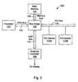
- FIG. 2 illustrates one embodiment of a computer system.
- Computer system 200 includes a processor 101 coupled to a variety of system components through a bus bridge 102.
- a main memory 104 is coupled to bus bridge 102 through a memory bus 106.
- a graphics controller 108 is coupled to bus bridge 102 through an AGP bus 110.
- a plurality of PCI (Peripheral Component Interconnect) devices 112A-112B are coupled to bus bridge 102 through a PCI bus 114.
- PCI Peripheral Component Interconnect
- Processor 101 is illustrative of, for example, an AthlonTM Microprocessor. It is understood, however, that in other embodiments of computer system 200, alternative types of microprocessors may be employed. In other embodiments, an external cache unit (not shown) may further be coupled to processor 101.
- Bus bridge 102 provides an interface between processor 101, main memory 104, graphics controller 108, and devices attached to PCI bus 114. When an operation is received from one of the devices connected to bus bridge 102, bus bridge 102 routes the operation to the targeted device. Bus bridge 102 generally translates an operation from the protocol used by the source device or bus to the protocol used by the target device or bus.
- Main memory 104 is a memory in which application programs and data are stored. Processor 101 executes primarily out of main memory 104.
- main memory 104 may be dynamic random access memory (DRAM) or preferably, in other embodiments, main memory 104 may be synchronous dynamic random access memory (SDRAM).
- DRAM dynamic random access memory
- SDRAM synchronous dynamic random access memory
- PCI devices 112A-112B are illustrative of a variety of peripheral devices such as, for example, network interface cards, video accelerators, audio cards, hard or floppy disk drives, small computer systems interface (SCSI) adapters and telephony cards.
- peripheral devices such as, for example, network interface cards, video accelerators, audio cards, hard or floppy disk drives, small computer systems interface (SCSI) adapters and telephony cards.
- SCSI small computer systems interface
- ISA device 118 is illustrative of one of a variety of peripheral devices such as a modem, a sound card, and a variety of data acquisition cards such as general purpose interface bus (GPIB) or field bus interface cards.
- GPS general purpose interface bus
- Graphics controller 108 is provided to control the rendering and images for a display device.
- Graphics controller 108 may embody a typical graphics accelerator generally known in the art to render three-dimensional data structures which can be effectively shifted into and out of main memory 104.
- Graphics controller 108 may therefore be a master of AGP bus 110 in that it can request and receive access to a target interface within bus bridge 102 and thereby obtain access to main memory 104.
- bus bridge 102 may receive requests from CPU bus 103, PCI bus 114 and AGP bus 110 to read from or write to main memory 104. Bus bridge 102 may categorize these requests according to a prioritization scheme which takes into account the priority of each request relative to each other request and the state of main memory 104 at the time of the request. In this manner, bus bridge 102 may advantageously optimize the utilization of the bandwidth of memory bus 106, thus increasing overall performance of the computer system.
- Bus bridge 102 includes a CPU interface 204, a PCI interface 212, an AGP interface 214 and a memory controller 210.
- Memory controller 210 is coupled to CPU interface 204, PCI interface 212 and AGP interface 214.
- Memory controller 210 is also coupled to a main memory 104 through memory bus 106. It is noted that the components of bus bridge 102 may be embodied on a single integrated circuit chip or they may be embodied within other components of computer system 200 of Figure 2.
- memory controller 210 uses a plurality of queues as a request buffering mechanism.
- the queues are configured to receive requests from CPU bus 103, PCI bus 114 and AGP bus 110 through CPU interface 204, PCI interface 212 and AGP interface 214, respectively.
- Memory controller 210 comprises an arbiter 310 which is coupled to a scheduler 320 and a graphics address remapping table (GART) table walk 330.
- Arbiter 310 is also coupled to CPU interface 204, PCI interface 212 and AGP interface 214.
- Scheduler 320 is coupled to main memory 104 through memory bus 106.
- Arbiter 310 includes a memory read queue (MRQ) 224, a memory write queue (MWQ) 222, an advanced graphics port queue (AGPQ) 226 and a priority logic block 315.
- Arbiter 310 may be configured to receive external memory requests from CPU interface 204, PCI interface 212 and AGP interface 214.
- Arbiter 310 may also be configured to receive one internal memory request from GART table walk 330 and one bypass request (BYP). The external requests are stored in one of MRQ 224, MWQ 224 or AGPQ 226.
- MRQ 224 stores requests to read from main memory 104.
- MWQ 222 stores requests to write to main memory 104 and
- AGPQ 226 stores requests to read from or write to main memory 104.
- MRQ 224 may be embodied in four separate buffers to accommodate up to four memory read requests. It is described here as one queue for the sake of simplicity. The size of MWQ is one entry and the size of AGPQ is one entry. It is noted however that in various other embodiments, the sizes of MRQ 224, MWQ 222 and AGPQ 226 may be different.
- Priority logic block 315 selects and presents one of the requests to scheduler 320 according to a fixed priority which is described further below. Scheduler 320 then schedules the request, either read or write, onto memory bus 106.
- main memory 104 is embodied in SDRAM.
- SDRAM accesses typically occur in page mode. These page mode accesses may be categorized into page hit requests (PH), page miss bank requests (PMb), page miss different chip select requests (PMc) and page conflict requests (PC). The priority given to the requests is based on the latency associated with each type of request.
- Priority logic block 315 includes categorizing multiplexers 410A, 410B, 410C and 410D which use combinational logic to categorize a plurality of requests received from MRQ 224, MWQ 222 and AGPQ 226 of Figure 4 into the four categories described above: page hit (PH), page miss bank (PMB), page miss-different chip select (PMC) and page conflict (PC).
- categorizing multiplexers 410A, 410B, 410C and 410D may each be referred to as categorizing multiplexer 410.
- Categorizing multiplexers 410 are configured to select one request from each category, (e.g. PH, PMb, PMc and PC), based on a categorizing scheme as illustrated in Figure 6.
- the outputs of categorizing multiplexers 410 are input to a priority select multiplexer 420.
- Priority select multiplexer 420 selects the next request to be scheduled to scheduler 320.
- Priority select multiplexer 420 selects from the following external/internal requests: an opportunistic precharge (OP), a high priority request from AGP interface 214 (Hi AGP), a high priority memory write request(Hi MWQ), an internal request from Gart Table Walk (GTW) 330 as well as the four categorized requests (PH, PMb, PMc, PC) from categorizing multiplexers 410, and an internal idle precharge signal.
- OP opportunistic precharge
- Hi AGP high priority request from AGP interface 214
- Hi MWQ high priority memory write request(Hi MWQ)
- GTW Gart Table Walk
- Priority select multiplexer 420 prioritizes the output requests from categorizing multiplexers 410 (e.g. PH's, PMb's, PMc's and PC's) based on the latency exhibited by these requests. As stated earlier, PH requests receive a higher arbitration priority over PMb, PMc and PC requests. However, to prevent starvation of service to requests with a lesser priority, priority select multiplexer 420 may be configured to stop servicing PH requests when a predetermined limit is reached. Priority select multiplexer 420 may include a programmable logic unit 421 which limits the number of page hit requests serviced consecutively from one to thirty-two.
- Programmable logic unit 421 includes a limit register 422 configured to store the PH request limit and a counter 423 coupled to limit register 422.
- Counter 423 is configured to count the number of priority hits that were serviced by scheduler 320 consecutively. Once counter 423 reaches the programmable limit, priority select multiplexer 420 may select a different request, for example, a PMb or a PMc. Counter 423 will then be reset to zero and will begin recounting the number of priority hits serviced by scheduler 320 consecutively.
- Categorizing multiplexer 410 uses combinational logic comprising a plurality of multiplexers to select the highest priority request. It is noted that other embodiments may use other logic blocks and configurations.
- Categorizing multiplexer 410 also includes an internal signal to indicate that neither AGPQ request nor MWQ request is valid. This internal request is called an invalid category pointer (INV).
- INV invalid category pointer
- Multiplexer 610 provides requests from MRQ0 a higher priority than requests from memory read queue 1, MRQ1.
- Multiplexer 620 provides requests from memory read queue 2, MRQ2, a higher priority than requests from memory read queue 3, MRQ3.
- Multiplexer 630 provides requests from MRQ0 and MRQ1 a higher priority than requests from MRQ2 and MRQ3.
- Multiplexer 640 provides requests from MWQ, a higher priority than requests from AGPQ.
- Multiplexer 640 further provides requests from AGPQ a higher priority than invalid category pointer.
- Multiplexer 650 provides requests from MRQ0-3, a higher priority than requests from MWQ and AGPQ.
- the output of categorizing multiplexer 410 is a valid category request pointer for input into priority select multiplexer 420 of Figure 4.
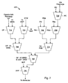
- Priority select multiplexer 420 assigns its incoming requests a priority from highest to lowest as follows: bypass (BYP), OP, Hi MWQ, Hi AGP, GTW, PH, PMb, PMc, PC and idle precharge.
- Multiplexer 710 gives OP a higher priority than Hi MWQ.
- Multiplexer 720 gives Hi AGP a higher priority than GTW.
- Multiplexer 730 gives PC a higher priority than idle precharge.
- Multiplexer 740 gives PH a higher priority over PMb.
- Multiplexer 750 gives PMc a higher priority than both PC and Idle Precharge.
- Multiplexer 760 gives Precharge and Hi MWQ a higher priority than Hi AGP and GTW.
- Multiplexer 770 gives PH and PMb a higher priority than PMc, PC and Idle Precharge.
- Multiplexer 780 gives Precharge, Hi MWQ, Hi AGP and GTW a higher priority than PH, PMB, PMC, PC and idle precharge.
- Multiplexer 790 gives Bypass the highest priority. The output of multiplexer 790 is the selected request sent to scheduler 320.
- the BYP request is issued only when there are no current valid chip selects. This may occur when memory controller 210 is completely idle. Since no chip select signal is currently valid, a PMc request will be treated as a PMb request. Whenever a BYP request is accepted, the BYP request may pass directly through scheduler 320 of Figure 5 and onto the memory bus 106 of Figure 4 in one cycle.
- BYP is given highest priority since the request may be placed on memory bus 106 in one cycle. However, the instances in which memory controller is completely idle may be rare.
- the OP request is given second highest priority of all other requests. OP is issued only one cycle after an 8 quad word PH or PMb request has been accepted to reduce the probability that a PC request will occur.
- the idle precharge request is issued when no new valid requests have been presented to arbiter 310 for more than a programmable number of cycles and therefore it is given the lowest priority of all requests.
- FIG 8 illustrates one embodiment of scheduler 320 of Figure 5. Circuit components that correspond to those shown in Figures 2 through 7 are numbered identically for simplicity and clarity.
- Scheduler 320 schedules the requests received from priority select multiplexer 420 of Figure 5 onto memory bus 106 of Figure 8.
- Scheduler 320 comprises three queues coupled to a priority multiplexer 840. The three queues are: a pre-charge queue (PQ) 820, an activate queue (AQ) 810 and a read/write queue (RWQ) 830.
- Scheduler 320 may be configured to provide PQ 820 with the highest priority followed by AQ 810 followed by RWQ 830.
- a request to initiate an OP cycle is loaded into PQ 820.
- a request to initiate an activation cycle is loaded into AQ 810.
- a request to initiate a read/write cycle is loaded into RWQ 830.
- the size of AQ 810 and PQ 820 is one deep.
- the size of RWQ 830 is 3 deep. The depth of one forces scheduler to accept the next request at the latest possible time before the last request is finished processing and memory bus 106 becomes idle. Waiting until the latest possible time to accept the next request from arbiter 310 of Figure 5 gives arbiter 310 the opportunity to examine more requests, thereby increasing the probability that a PH or PMb request will be presented. It is noted however, that the size of the queues in scheduler 320 of Figure 8 may be varied in different embodiments.
- each bank of SDRAM module 16A-C includes a plurality of pages that are accessed by a particular memory access address.
- one or more cycles will be initiated by scheduler 320 of Figure 8 to access the requested page.
- scheduler 320 receives a PH request
- a request to initiate a read/write cycle is loaded in RWQ 830 of Figure 8.
- RWQ 830 of Figure 8.
- scheduler 320 receives a PMb request
- a request to initiate both an activation cycle and a read/write cycle will be loaded in AQ 810 and RWQ 830, respectively.
- AQ 810 has a higher priority than RWQ 830
- the activation cycle will be initiated before the read/write cycle.
- scheduler 320 receives a PMc request, a request to initiate an activation cycle and a read/write cycle will also be loaded in activate queue 810 and read/write queue 830, respectively. After the one cycle turnaround bubble described in the description of Figure 1, scheduler 320 of Figure 8 will initiate an activation cycle followed by a read/write cycle.
- scheduler 320 receives a PC request, a request to initiate a precharge cycle, an activation cycle and a read/write cycle will be loaded in PQ 820, AQ 820 and RWQ 830 respectively. Since PQ 820 has the highest priority, the precharge cycle will execute first, then the activation cycle followed by the read/write cycle. However, since PC requests typically offer the worst latency, a PC request may be converted to an OP request followed by a PMb request This allows more optimal requests that are received later than the PC to be interleaved between the OP and the PMb.
- scheduler 320 may therefore pass this request through AQ 820 to memory bus 106 in one cycle.
- scheduler 320 may also be configured to control various other SDRAM related activities including: refresh cycles to the SDRAM, initialization and configuration of the SDRAM out of reset and power up and power down of the SDRAM.
- This invention is applicable to computer systems.
Description
Claims (10)
- A bus bridge (102) comprising:wherein said memory controller (210) is configured to accept and arbitrate a plurality of incoming requests from said processor bus interface (204) and said first peripheral bus interface (212), characterised in that said memory controller (210) categorizes said plurality of incoming requests into a page hit request, a page miss bank request and a page miss-different chip select request, wherein said memory controller (210) is configured to provide said page hit request with a higher arbitration priority than said page miss bank request, and wherein said memory controller (210) is configured to provide said page miss bank request with a higher arbitration priority than said page miss-different chip select request.a memory controller (210) for controlling accesses to a memory (104);a processor bus interface (204) coupled to said memory controller (210), wherein said processor bus interface (204) provides an interface between said memory controller (210) and a processor (101);a first peripheral bus interface (212) coupled to said memory controller (210), wherein said first peripheral bus interface provides an interface between said memory controller (210) and a first peripheral bus (114);
- The bus bridge (102) as recited in claim 1, wherein said memory (104) is coupled to said bus bridge (102) through a memory bus (106), wherein said memory bus (106) is a synchronous dynamic random access memory bus.
- The bus bridge (102) as recited in claim 1, wherein said memory controller (210) comprises:an arbiter (310) which is configured to arbitrate between said incoming requests, wherein said arbiter (310) comprises a plurality of categorizing multiplexers (410) configured to categorize said plurality of incoming requests.
- The bus bridge (102) as recited in claim 3, wherein each one of said plurality of categorizing multiplexers (410) is a multiplexing unit, wherein each multiplexing unit comprises a plurality of multiplexers (610-650) which are configured to select one request from said plurality of incoming requests.
- The bus bridge (102) as recited in claim 4, wherein said arbiter (310) further comprises:a priority select multiplexer unit (420) coupled to receive a plurality of categorized incoming requests from said plurality of categorizing multiplexers, wherein said priority select multiplexer unit (420) is configured to select a priority request to be scheduled based on a fixed priority, wherein said priority select multiplexer unit (420) comprises a plurality of multiplexers (710-790).
- The bus bridge (102) as recited in claim 5, wherein said memory controller (210) further comprises:a scheduler (320) coupled to receive said priority request selected by said priority select multiplexer unit (420), wherein said scheduler (320) is configured to schedule said priority request onto said synchronous dynamic random access memory bus, wherein said scheduler comprises a pre-charge queue (820), an activate queue (810), and a read/write queue (830), wherein a precharge cycle is loaded into said pre-charge queue, wherein an activation cycle is loaded into said activate queue, wherein a read/write cycle is loaded into said read/write queue.
- The bus bridge (102) as recited in claim 1, wherein said memory controller (210) is further configured to categorize said plurality of incoming requests into a page conflict request, wherein said memory controller (210) is configured to provide said miss bank-different chip select request with a higher arbitration priority than said page conflict request.
- The bus bridge (102) as recited in claim 7, wherein said plurality of incoming requests comprises:at least one request from said processor bus interface (204);at least one request from said first peripheral bus interface (212);at least one request from said second peripheral bus interface (214); andat least one request from a graphics address remapping table (GART) table walk (330).
- A method of operating a memory controller (210) comprising:receiving incoming requests from a processor bus interface (204), and a first peripheral bus interface (212);categorizing said incoming requests into a plurality of categories, wherein said plurality of categories comprise a page hit request, a page miss bank request, and a page miss-different chip select request;prioritizing among said incoming requests, wherein said page hit request receives a higher arbitration priority than said page miss bank request, wherein said page miss bank request receives a higher arbitration priority than said page miss-different chip select request.
- A computer system comprising:wherein said bus bridge (102) comprises a memory controller (210), wherein said memory controller (210) is configured to accept and arbitrate a plurality of incoming requests from said processor bus interface (204), said first peripheral bus interface (212) and said second peripheral bus interface (214), characterised in that said memory controller (210) categorizes said plurality of incoming requests into a page hit request, a page miss bank request and a page miss-different chip select request, wherein said memory controller (210) is configured to provide said page hit request with a higher arbitration priority than said page miss bank request, wherein said memory controller (210) is configured to provide said page miss bank request with a higher arbitration priority than said page miss-different chip select request.a microprocessor (101) coupled to a processor bus interface (204), wherein said microprocessor (101) generates one or more requests;a main memory (104) coupled to a memory bus interface;a bus bridge (102) coupled to provide an interface between said processor bus interface (204), said memory bus interface, a first peripheral bus interface (212), and a second peripheral bus interface (214), wherein said first peripheral bus interface (212) generates at least one request, wherein said second peripheral bus interface (214) generates at least one request;
Applications Claiming Priority (3)
| Application Number | Priority Date | Filing Date | Title |
|---|---|---|---|
| US54123400A | 2000-04-03 | 2000-04-03 | |
| US541234 | 2000-04-03 | ||
| PCT/US2000/031963 WO2001075620A1 (en) | 2000-04-03 | 2000-11-21 | Bus bridge including a memory controller having an improved memory request arbitration mechanism |
Publications (2)
| Publication Number | Publication Date |
|---|---|
| EP1269330A1 EP1269330A1 (en) | 2003-01-02 |
| EP1269330B1 true EP1269330B1 (en) | 2004-03-24 |
Family
ID=24158732
Family Applications (1)
| Application Number | Title | Priority Date | Filing Date |
|---|---|---|---|
| EP00980619A Expired - Lifetime EP1269330B1 (en) | 2000-04-03 | 2000-11-21 | Bus bridge including a memory controller having an improved memory request arbitration mechanism |
Country Status (6)
| Country | Link |
|---|---|
| EP (1) | EP1269330B1 (en) |
| JP (1) | JP2004500667A (en) |
| KR (1) | KR20020089428A (en) |
| CN (1) | CN1452745A (en) |
| DE (1) | DE60009355T2 (en) |
| WO (1) | WO2001075620A1 (en) |
Families Citing this family (23)
| Publication number | Priority date | Publication date | Assignee | Title |
|---|---|---|---|---|
| US6578117B2 (en) * | 2001-10-12 | 2003-06-10 | Sonics, Inc. | Method and apparatus for scheduling requests using ordered stages of scheduling criteria |
| US6961834B2 (en) * | 2001-10-12 | 2005-11-01 | Sonics, Inc. | Method and apparatus for scheduling of requests to dynamic random access memory device |
| US7194561B2 (en) * | 2001-10-12 | 2007-03-20 | Sonics, Inc. | Method and apparatus for scheduling requests to a resource using a configurable threshold |
| US6804738B2 (en) | 2001-10-12 | 2004-10-12 | Sonics, Inc. | Method and apparatus for scheduling a resource to meet quality-of-service restrictions |
| US7020762B2 (en) * | 2002-12-24 | 2006-03-28 | Intel Corporation | Method and apparatus for determining a dynamic random access memory page management implementation |
| KR100518576B1 (en) * | 2003-05-24 | 2005-10-04 | 삼성전자주식회사 | Bus arbiter and bus arbitrating method |
| US9087036B1 (en) | 2004-08-12 | 2015-07-21 | Sonics, Inc. | Methods and apparatuses for time annotated transaction level modeling |
| US7665069B2 (en) | 2003-10-31 | 2010-02-16 | Sonics, Inc. | Method and apparatus for establishing a quality of service model |
| KR100690621B1 (en) * | 2005-02-04 | 2007-03-09 | 엘지전자 주식회사 | Method for arbitrating bus |
| KR100784385B1 (en) * | 2005-08-10 | 2007-12-11 | 삼성전자주식회사 | System and method of arbitrating requests for a shared resource |
| JP2008017441A (en) | 2006-06-06 | 2008-01-24 | Ricoh Co Ltd | Data processing apparatus, data processing method, and program |
| US8868397B2 (en) | 2006-11-20 | 2014-10-21 | Sonics, Inc. | Transaction co-validation across abstraction layers |
| US20080162852A1 (en) * | 2006-12-28 | 2008-07-03 | Surya Kareenahalli | Tier-based memory read/write micro-command scheduler |
| JP5034551B2 (en) * | 2007-02-26 | 2012-09-26 | 富士通セミコンダクター株式会社 | Memory controller, semiconductor memory access control method and system |
| KR100973419B1 (en) * | 2008-06-11 | 2010-07-30 | 인하대학교 산학협력단 | Method and apparatus for arbitrating a bus |
| US8615637B2 (en) * | 2009-09-10 | 2013-12-24 | Advanced Micro Devices, Inc. | Systems and methods for processing memory requests in a multi-processor system using a probe engine |
| US8838901B2 (en) | 2010-05-07 | 2014-09-16 | International Business Machines Corporation | Coordinated writeback of dirty cachelines |
| US8683128B2 (en) | 2010-05-07 | 2014-03-25 | International Business Machines Corporation | Memory bus write prioritization |
| KR20140028618A (en) | 2012-08-29 | 2014-03-10 | 삼성전자주식회사 | Memory device for reducimg write fail, system includinmg tha same, and method there-of |
| KR102098248B1 (en) | 2013-06-03 | 2020-04-07 | 삼성전자 주식회사 | Memory controller using a memory device with released timing specification according to temperature |
| CN104765577B (en) * | 2015-04-28 | 2017-08-15 | 杭州中天微系统有限公司 | A kind of adaptive high-speed memory system of frequency |
| CN106528464A (en) * | 2016-11-08 | 2017-03-22 | 英业达科技有限公司 | Computer system with memory access conflict control |
| CN109491785B (en) * | 2018-10-24 | 2021-01-26 | 龙芯中科技术股份有限公司 | Memory access scheduling method, device and equipment |
Family Cites Families (4)
| Publication number | Priority date | Publication date | Assignee | Title |
|---|---|---|---|---|
| US5222223A (en) * | 1989-02-03 | 1993-06-22 | Digital Equipment Corporation | Method and apparatus for ordering and queueing multiple memory requests |
| US5638534A (en) * | 1995-03-31 | 1997-06-10 | Samsung Electronics Co., Ltd. | Memory controller which executes read and write commands out of order |
| US5745913A (en) * | 1996-08-05 | 1998-04-28 | Exponential Technology, Inc. | Multi-processor DRAM controller that prioritizes row-miss requests to stale banks |
| EP0924621A3 (en) * | 1997-12-22 | 2000-06-28 | Compaq Computer Corporation | Computer system including bridge logic having a fair arbitration mechanism to support isochronous devices |
-
2000
- 2000-11-21 KR KR1020027013238A patent/KR20020089428A/en not_active Application Discontinuation
- 2000-11-21 EP EP00980619A patent/EP1269330B1/en not_active Expired - Lifetime
- 2000-11-21 DE DE60009355T patent/DE60009355T2/en not_active Expired - Fee Related
- 2000-11-21 JP JP2001573232A patent/JP2004500667A/en not_active Withdrawn
- 2000-11-21 CN CN 00819403 patent/CN1452745A/en active Pending
- 2000-11-21 WO PCT/US2000/031963 patent/WO2001075620A1/en active IP Right Grant
Also Published As
| Publication number | Publication date |
|---|---|
| JP2004500667A (en) | 2004-01-08 |
| DE60009355T2 (en) | 2005-02-24 |
| WO2001075620A1 (en) | 2001-10-11 |
| EP1269330A1 (en) | 2003-01-02 |
| DE60009355D1 (en) | 2004-04-29 |
| KR20020089428A (en) | 2002-11-29 |
| CN1452745A (en) | 2003-10-29 |
Similar Documents
| Publication | Publication Date | Title |
|---|---|---|
| EP1269330B1 (en) | Bus bridge including a memory controller having an improved memory request arbitration mechanism | |
| US6505260B2 (en) | Computer system with adaptive memory arbitration scheme | |
| US6006303A (en) | Priority encoding and decoding for memory architecture | |
| US7617368B2 (en) | Memory interface with independent arbitration of precharge, activate, and read/write | |
| US6269433B1 (en) | Memory controller using queue look-ahead to reduce memory latency | |
| US6412048B1 (en) | Traffic controller using priority and burst control for reducing access latency | |
| US5655151A (en) | DMA controller having a plurality of DMA channels each having multiple register sets storing different information controlling respective data transfer | |
| US6393506B1 (en) | Virtual channel bus and system architecture | |
| EP1540485B1 (en) | Out of order dram sequencer | |
| EP2430554B1 (en) | Hierarchical memory arbitration technique for disparate sources | |
| US6330646B1 (en) | Arbitration mechanism for a computer system having a unified memory architecture | |
| US8095744B2 (en) | Device for controlling access from a plurality of masters to shared memory composed of a plurality of banks each having a plurality of pages | |
| US7363406B2 (en) | Dynamic access scheduling memory controller | |
| US5475829A (en) | Computer system which overrides write protection status during execution in system management mode | |
| US10783104B2 (en) | Memory request management system | |
| US7127573B1 (en) | Memory controller providing multiple power modes for accessing memory devices by reordering memory transactions | |
| US20040193779A1 (en) | Memory controller | |
| US6523098B1 (en) | Mechanism for efficient low priority write draining | |
| US8271746B1 (en) | Tiering of linear clients | |
| US6233661B1 (en) | Computer system with memory controller that hides the next cycle during the current cycle | |
| US6360305B1 (en) | Method and apparatus for optimizing memory performance with opportunistic pre-charging | |
| US20110197008A1 (en) | Card host lsi and set device including the lsi | |
| JP5058116B2 (en) | DMAC issue mechanism by streaming ID method | |
| US20080098153A1 (en) | Memory access controller | |
| JP3235578B2 (en) | Memory access control method |
Legal Events
| Date | Code | Title | Description |
|---|---|---|---|
| PUAI | Public reference made under article 153(3) epc to a published international application that has entered the european phase |
Free format text: ORIGINAL CODE: 0009012 |
|
| 17P | Request for examination filed |
Effective date: 20020918 |
|
| AK | Designated contracting states |
Kind code of ref document: A1 Designated state(s): AT BE CH CY DE DK ES FI FR GB GR IE IT LI LU MC NL PT SE TR |
|
| AX | Request for extension of the european patent |
Free format text: AL;LT;LV;MK;RO;SI |
|
| RIN1 | Information on inventor provided before grant (corrected) |
Inventor name: NOVAK, STEVE |
|
| GRAP | Despatch of communication of intention to grant a patent |
Free format text: ORIGINAL CODE: EPIDOSNIGR1 |
|
| GRAS | Grant fee paid |
Free format text: ORIGINAL CODE: EPIDOSNIGR3 |
|
| GRAA | (expected) grant |
Free format text: ORIGINAL CODE: 0009210 |
|
| AK | Designated contracting states |
Kind code of ref document: B1 Designated state(s): DE GB |
|
| REG | Reference to a national code |
Ref country code: GB Ref legal event code: FG4D |
|
| REG | Reference to a national code |
Ref country code: IE Ref legal event code: FG4D |
|
| REF | Corresponds to: |
Ref document number: 60009355 Country of ref document: DE Date of ref document: 20040429 Kind code of ref document: P |
|
| LTIE | Lt: invalidation of european patent or patent extension |
Effective date: 20040324 |
|
| PGFP | Annual fee paid to national office [announced via postgrant information from national office to epo] |
Ref country code: GB Payment date: 20041004 Year of fee payment: 5 |
|
| PGFP | Annual fee paid to national office [announced via postgrant information from national office to epo] |
Ref country code: DE Payment date: 20041130 Year of fee payment: 5 |
|
| PLBE | No opposition filed within time limit |
Free format text: ORIGINAL CODE: 0009261 |
|
| STAA | Information on the status of an ep patent application or granted ep patent |
Free format text: STATUS: NO OPPOSITION FILED WITHIN TIME LIMIT |
|
| 26N | No opposition filed |
Effective date: 20041228 |
|
| PG25 | Lapsed in a contracting state [announced via postgrant information from national office to epo] |
Ref country code: GB Free format text: LAPSE BECAUSE OF NON-PAYMENT OF DUE FEES Effective date: 20051121 |
|
| PG25 | Lapsed in a contracting state [announced via postgrant information from national office to epo] |
Ref country code: DE Free format text: LAPSE BECAUSE OF NON-PAYMENT OF DUE FEES Effective date: 20060601 |
|
| GBPC | Gb: european patent ceased through non-payment of renewal fee |
Effective date: 20051121 |