EP3822749A1 - Touch display device and method of manufacturing of the same - Google Patents
Touch display device and method of manufacturing of the same Download PDFInfo
- Publication number
- EP3822749A1 EP3822749A1 EP20200245.7A EP20200245A EP3822749A1 EP 3822749 A1 EP3822749 A1 EP 3822749A1 EP 20200245 A EP20200245 A EP 20200245A EP 3822749 A1 EP3822749 A1 EP 3822749A1
- Authority
- EP
- European Patent Office
- Prior art keywords
- electrode
- touch
- pad electrode
- layer
- pad
- Prior art date
- Legal status (The legal status is an assumption and is not a legal conclusion. Google has not performed a legal analysis and makes no representation as to the accuracy of the status listed.)
- Granted
Links
Images



Classifications
-
- G—PHYSICS
- G06—COMPUTING OR CALCULATING; COUNTING
- G06F—ELECTRIC DIGITAL DATA PROCESSING
- G06F3/00—Input arrangements for transferring data to be processed into a form capable of being handled by the computer; Output arrangements for transferring data from processing unit to output unit, e.g. interface arrangements
- G06F3/01—Input arrangements or combined input and output arrangements for interaction between user and computer
- G06F3/03—Arrangements for converting the position or the displacement of a member into a coded form
- G06F3/041—Digitisers, e.g. for touch screens or touch pads, characterised by the transducing means
- G06F3/0412—Digitisers structurally integrated in a display
-
- G—PHYSICS
- G06—COMPUTING OR CALCULATING; COUNTING
- G06F—ELECTRIC DIGITAL DATA PROCESSING
- G06F3/00—Input arrangements for transferring data to be processed into a form capable of being handled by the computer; Output arrangements for transferring data from processing unit to output unit, e.g. interface arrangements
- G06F3/01—Input arrangements or combined input and output arrangements for interaction between user and computer
- G06F3/03—Arrangements for converting the position or the displacement of a member into a coded form
- G06F3/041—Digitisers, e.g. for touch screens or touch pads, characterised by the transducing means
- G06F3/044—Digitisers, e.g. for touch screens or touch pads, characterised by the transducing means by capacitive means
- G06F3/0448—Details of the electrode shape, e.g. for enhancing the detection of touches, for generating specific electric field shapes, for enhancing display quality
-
- G—PHYSICS
- G06—COMPUTING OR CALCULATING; COUNTING
- G06F—ELECTRIC DIGITAL DATA PROCESSING
- G06F3/00—Input arrangements for transferring data to be processed into a form capable of being handled by the computer; Output arrangements for transferring data from processing unit to output unit, e.g. interface arrangements
- G06F3/01—Input arrangements or combined input and output arrangements for interaction between user and computer
- G06F3/03—Arrangements for converting the position or the displacement of a member into a coded form
- G06F3/041—Digitisers, e.g. for touch screens or touch pads, characterised by the transducing means
- G06F3/0414—Digitisers, e.g. for touch screens or touch pads, characterised by the transducing means using force sensing means to determine a position
- G06F3/04144—Digitisers, e.g. for touch screens or touch pads, characterised by the transducing means using force sensing means to determine a position using an array of force sensing means
-
- G—PHYSICS
- G06—COMPUTING OR CALCULATING; COUNTING
- G06F—ELECTRIC DIGITAL DATA PROCESSING
- G06F3/00—Input arrangements for transferring data to be processed into a form capable of being handled by the computer; Output arrangements for transferring data from processing unit to output unit, e.g. interface arrangements
- G06F3/01—Input arrangements or combined input and output arrangements for interaction between user and computer
- G06F3/03—Arrangements for converting the position or the displacement of a member into a coded form
- G06F3/041—Digitisers, e.g. for touch screens or touch pads, characterised by the transducing means
- G06F3/0416—Control or interface arrangements specially adapted for digitisers
- G06F3/04164—Connections between sensors and controllers, e.g. routing lines between electrodes and connection pads
-
- G—PHYSICS
- G06—COMPUTING OR CALCULATING; COUNTING
- G06F—ELECTRIC DIGITAL DATA PROCESSING
- G06F3/00—Input arrangements for transferring data to be processed into a form capable of being handled by the computer; Output arrangements for transferring data from processing unit to output unit, e.g. interface arrangements
- G06F3/01—Input arrangements or combined input and output arrangements for interaction between user and computer
- G06F3/03—Arrangements for converting the position or the displacement of a member into a coded form
- G06F3/041—Digitisers, e.g. for touch screens or touch pads, characterised by the transducing means
- G06F3/044—Digitisers, e.g. for touch screens or touch pads, characterised by the transducing means by capacitive means
- G06F3/0445—Digitisers, e.g. for touch screens or touch pads, characterised by the transducing means by capacitive means using two or more layers of sensing electrodes, e.g. using two layers of electrodes separated by a dielectric layer
-
- G—PHYSICS
- G06—COMPUTING OR CALCULATING; COUNTING
- G06F—ELECTRIC DIGITAL DATA PROCESSING
- G06F3/00—Input arrangements for transferring data to be processed into a form capable of being handled by the computer; Output arrangements for transferring data from processing unit to output unit, e.g. interface arrangements
- G06F3/01—Input arrangements or combined input and output arrangements for interaction between user and computer
- G06F3/03—Arrangements for converting the position or the displacement of a member into a coded form
- G06F3/041—Digitisers, e.g. for touch screens or touch pads, characterised by the transducing means
- G06F3/044—Digitisers, e.g. for touch screens or touch pads, characterised by the transducing means by capacitive means
- G06F3/0446—Digitisers, e.g. for touch screens or touch pads, characterised by the transducing means by capacitive means using a grid-like structure of electrodes in at least two directions, e.g. using row and column electrodes
-
- G—PHYSICS
- G09—EDUCATION; CRYPTOGRAPHY; DISPLAY; ADVERTISING; SEALS
- G09F—DISPLAYING; ADVERTISING; SIGNS; LABELS OR NAME-PLATES; SEALS
- G09F9/00—Indicating arrangements for variable information in which the information is built-up on a support by selection or combination of individual elements
- G09F9/30—Indicating arrangements for variable information in which the information is built-up on a support by selection or combination of individual elements in which the desired character or characters are formed by combining individual elements
- G09F9/301—Indicating arrangements for variable information in which the information is built-up on a support by selection or combination of individual elements in which the desired character or characters are formed by combining individual elements flexible foldable or roll-able electronic displays, e.g. thin LCD, OLED
-
- H—ELECTRICITY
- H10—SEMICONDUCTOR DEVICES; ELECTRIC SOLID-STATE DEVICES NOT OTHERWISE PROVIDED FOR
- H10K—ORGANIC ELECTRIC SOLID-STATE DEVICES
- H10K59/00—Integrated devices, or assemblies of multiple devices, comprising at least one organic light-emitting element covered by group H10K50/00
- H10K59/10—OLED displays
- H10K59/12—Active-matrix OLED [AMOLED] displays
-
- H—ELECTRICITY
- H10—SEMICONDUCTOR DEVICES; ELECTRIC SOLID-STATE DEVICES NOT OTHERWISE PROVIDED FOR
- H10K—ORGANIC ELECTRIC SOLID-STATE DEVICES
- H10K59/00—Integrated devices, or assemblies of multiple devices, comprising at least one organic light-emitting element covered by group H10K50/00
- H10K59/40—OLEDs integrated with touch screens
-
- H—ELECTRICITY
- H10—SEMICONDUCTOR DEVICES; ELECTRIC SOLID-STATE DEVICES NOT OTHERWISE PROVIDED FOR
- H10K—ORGANIC ELECTRIC SOLID-STATE DEVICES
- H10K59/00—Integrated devices, or assemblies of multiple devices, comprising at least one organic light-emitting element covered by group H10K50/00
- H10K59/80—Constructional details
- H10K59/87—Passivation; Containers; Encapsulations
- H10K59/873—Encapsulations
-
- H—ELECTRICITY
- H10—SEMICONDUCTOR DEVICES; ELECTRIC SOLID-STATE DEVICES NOT OTHERWISE PROVIDED FOR
- H10K—ORGANIC ELECTRIC SOLID-STATE DEVICES
- H10K71/00—Manufacture or treatment specially adapted for the organic devices covered by this subclass
-
- G—PHYSICS
- G06—COMPUTING OR CALCULATING; COUNTING
- G06F—ELECTRIC DIGITAL DATA PROCESSING
- G06F2203/00—Indexing scheme relating to G06F3/00 - G06F3/048
- G06F2203/041—Indexing scheme relating to G06F3/041 - G06F3/045
- G06F2203/04102—Flexible digitiser, i.e. constructional details for allowing the whole digitising part of a device to be flexed or rolled like a sheet of paper
-
- G—PHYSICS
- G06—COMPUTING OR CALCULATING; COUNTING
- G06F—ELECTRIC DIGITAL DATA PROCESSING
- G06F2203/00—Indexing scheme relating to G06F3/00 - G06F3/048
- G06F2203/041—Indexing scheme relating to G06F3/041 - G06F3/045
- G06F2203/04103—Manufacturing, i.e. details related to manufacturing processes specially suited for touch sensitive devices
-
- G—PHYSICS
- G06—COMPUTING OR CALCULATING; COUNTING
- G06F—ELECTRIC DIGITAL DATA PROCESSING
- G06F2203/00—Indexing scheme relating to G06F3/00 - G06F3/048
- G06F2203/041—Indexing scheme relating to G06F3/041 - G06F3/045
- G06F2203/04112—Electrode mesh in capacitive digitiser: electrode for touch sensing is formed of a mesh of very fine, normally metallic, interconnected lines that are almost invisible to see. This provides a quite large but transparent electrode surface, without need for ITO or similar transparent conductive material
Definitions
- the present disclosure relates to a touch display device, and more particularly, to a touch display device being capable of minimizing a defect and a manufacturing method of the touch display device.
- a touch sensor is installed in a flat panel display device, e.g., a liquid crystal display (LCD) device, a field emission display (FED) device, a plasma display panel (PDP), an electroluminescent display device or an electrophoretic display device, and is an input device to input predetermined information by user's press or touch while viewing the display device.
- a flat panel display device e.g., a liquid crystal display (LCD) device, a field emission display (FED) device, a plasma display panel (PDP), an electroluminescent display device or an electrophoretic display device, and is an input device to input predetermined information by user's press or touch while viewing the display device.
- the touch senor for the display devices may be classified into an add-on type touch screen panel (touch sensor), an on-cell type touch screen panel and an integrated type (or an in-cell type) touch screen panel.
- touch screen panel In the add-on type touch screen panel, after a display panel and a touch screen panel are independently manufactured, the touch screen panel is attached on an upper substrate of the display panel.
- the touch screen panel In the on-cell type touch screen panel, elements (or members) for the touch sensor are formed on a surface of an upper substrate of a display panel.
- the touch sensor is included inside a display panel.
- the touch sensor or the touch screen panel is widely applied to an organic light emitting display (OLED) device as the flexible or foldable display device.
- OLED organic light emitting display
- touch sensor used for a flexible, bendable, or foldable touch display device various types of touch sensors, i.e., the add-on type, the on-cell type or the integrated type, can be used.
- the add-on type touch display device which is manufactured by attaching the touch panel on the display panel, is relatively thick, it is difficult to realize a flexible or foldable display device.
- the integrated type touch sensor is most frequently used for the flexible or foldable OLED device.
- an encapsulation layer which includes an organic material and/or an inorganic material, is required in the OLED device to minimize moisture or oxygen penetration, a manufacturing method of the integrated touch OLED device is complicated.
- the integrated type touch OLED device may be easily damaged by the bending stress which may occur in a folding operation.
- the touch sensor may be disposed or bonded on the encapsulation layer.
- the on-cell type touch sensor can be applied to display devices other than the OLED device.
- the touch sensor is electrically connected to a pad region for transmitting and receiving data.
- the pad region is disposed on the outside, not on the inside, where the touch sensor and the display substrate are bonded.
- defects may occur due to the above-mentioned structure.
- a step of bonding the touch sensor on the temporary manufacturing substrate with the display panel is performed.
- the temporary manufacturing substrate is removed (separated).
- the pad region for transmitting and receiving data of the touch sensor may not be smoothly separated from the temporary manufacturing substrate such that defects may be generated.
- the present disclosure is directed to a touch display device and a manufacturing method of the same that substantially obviate one or more of the problems due to limitations and disadvantages of the related art, and have other advantages.
- An aspect of the present disclosure is a touch display device comprising: a plurality of light emitting elements; an adhesive layer over the light emitting elements; a first touch electrode and a second touch electrode over the adhesive layer and in an active area; a pad electrode over the adhesive layer and in a touch pad region; and a protection layer over the first touch electrode, the second touch electrode and the pad electrode, wherein the first touch electrode and the second touch electrode are insulated by an insulating layer, and the protection layer includes at least one contact hole corresponding to the pad electrode, and wherein the pad electrode includes a plurality of electrode layers, and one of the plurality of electrode layers extends from the first touch electrode or the second touch electrode.
- a surface of at least one of the plurality of electrode layers is plasma-treated.
- an interface between a first electrode layer of the plurality of electrode layers at an uppermost position and a second electrode layer of the plurality of electrode layers is plasma-treated.
- the at least one contact hole has a pentagonal shape or a hexagonal shape.
- the pad electrode corresponds to two or more contact holes.
- the touch display device further comprises an encapsulation layer between the light emitting elements and the adhesion layer.
- each of the light emitting elements is an organic light emitting diode
- the encapsulation layer covers the organic light emitting diode
- the protection layer is formed of photo-acryl, and an inner surface of the contact hole has a reverse-tapered shape.
- the pad electrode includes a first pad electrode in the at least one contact hole, a second pad electrode contacting the first pad electrode, and a third pad electrode contacting the second pad electrode.
- the second pad electrode and the third pad electrode are respectively disposed on the same layer as the first touch electrode and the second touch electrode.
- an edge of the first pad electrode covers a side surface of the protection layer in the contact hole.
- the protection layer is disposed between the first pad electrode and the second pad electrode.
- Another aspect of the present disclosure is a method of manufacturing a touch display device comprising: forming a sacrificial layer on a temporary substrate; forming a protection layer including a contact hole in a touch pad region on the sacrificial layer; forming a first pad electrode in the touch pad region; forming a touch electrode on the protection layer and a second pad electrode on the first pad electrode; attaching the temporary substrate and a display substrate; and removing the temporary substrate and the sacrificial layer.
- the method further comprises: performing a plasma treatment to a portion of the protection layer.
- the plasma treatment uses one of an Ar gas plasma, an O 2 gas plasma, a H 2 gas plasma and a N 2 gas plasma.
- a portion of the first pad electrode is plasma-treated in the step of performing the plasma treatment.
- the step of removing the temporary substrate and the sacrificial layer includes irradiating a laser to reduce an adhesion strength of the sacrificial layer.
- a portion of the sacrificial layer is exposed through the contact hole.
- the first pad electrode contacts the portion of the sacrificial layer in the contact hole.
- the step of forming the first pad electrode is prior to the step of forming the protection layer.
- the protection layer covers edges of the first pad electrode.
- the contact hole has a pentagonal shape or a hexagonal shape.
- the method further comprises: forming an insulating layer covering the touch electrode, which is a first touch electrode, and exposing the second pad electrode; and forming a second touch electrode on the insulating layer and a third pad electrode on the second pad electrode, wherein one of the second pad electrode and the third pad electrode is electrically connected to one of the first touch electrode and the second touch electrode.
- the one of the second pad electrode and the third pad electrode extends from the one of the first touch electrode and the second touch electrode.
- the pad region may be damaged in the on-cell type touch display device.
- the inventors of the present disclosure have invented a touch display device (or a touch display apparatus) and a manufacturing method of the same being capable of minimizing defects that may occur in the process of manufacturing the touch display device including an on-cell type touch sensor.
- the present disclosure is to provide a touch display device being capable of minimizing defects that may occur in a manufacturing process for a pad region for transmitting and receiving touch-related data.
- the present disclosure is to provide a touch display device being capable of minimizing defect yield in a manufacturing process for a pad region for transmitting and receiving touch signal.
- Each of features of the various embodiments of the present disclosure may be partially or wholly combined or mixed with each other, and technically various interlocking and driving is possible.
- Each of the embodiments may be independently implemented with respect to each other or may be implemented together in an association relationship.
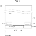
- FIG. 1 is a schematic plane view of a touch display device according to an embodiment of the present disclosure
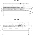
- FIGs. 2A and 2B are schematic cross-sectional views taken along the lines I-I' and II-II' of FIG. 1 , respectively.
- a touch display device 100 includes a display substrate DSP and a touch substrate TSP.
- the display substrate DSP may be an organic light emitting display substrate, but it is not limited thereto.
- the display substrate DSP may include a substrate PI, which includes an active area AA and first and second bezel areas BA1 and BA2, a light emitting element LS, which includes an anode, an organic emitting layer and a cathode, over the substrate PI and a thin film transistor (TFT) on the substrate PI for controlling the light emitting element LS according to a driving signal.
- a substrate PI which includes an active area AA and first and second bezel areas BA1 and BA2
- a light emitting element LS which includes an anode, an organic emitting layer and a cathode, over the substrate PI and a thin film transistor (TFT) on the substrate PI for controlling the light emitting element LS according to a driving signal.
- TFT thin film transistor
- the display substrate DSP and the touch substrate TSP may have a structure that is bonded by an adhesive layer AL, and the adhesive layer AL may be an epoxy-based adhesive layer.
- the adhesive layer AL may have a structure that is directly adjacent or directly contacts an encapsulation layer ENC of the display substrate DSP and a second insulating layer Passi of the touch substrate TSP.
- the organic emitting layer in the light emitting element LS is vulnerable to oxygen and moisture. Accordingly, the organic emitting layer may be covered by the encapsulation layer ENC to minimize the penetration of oxygen and moisture into the light emitting element LS.
- the encapsulation layer ENC may further include an absorbent or a nano-material for improving the light efficiency of light emitted from the light emitting element LS.
- the encapsulation layer ENC may include a plurality of layers, in which an organic material layer and an inorganic material layer are alternately stacked, and may further include various configurations for preventing cracks in order to provide a flexible display device. The explanation to this configuration is omitted.
- the light emitting element LS including the anode, the organic emitting layer, and the cathode is controlled by a circuit unit including the TFT. Electrical signals and current for such control may be supplied through a circuit board connected to a data pad DP.
- the light emitting element LS controls the amount of light, and various wavelengths of light can be emitted through a plurality of light emitting elements LS to display a desired image.
- the light emitting element (or, each of the light emitting elements) LS may further include a color filter layer.
- the substrate PI of the display substrate DSP may be a polyimide substrate to be used for a flexible display device or a foldable display device and may have a multi-layered structure.
- the display substrate DSP may further include a planarization layer FL for the arrangement of the light emitting elements LS.
- the planarization layer FL may be made of a material such as photo-acryl and may include a plurality of layers such that the light emitting elements LS, the TFT and the signal lines, e.g., the data lines, which are connected to the TFT, may be disposed on or over the planarization layer FL or between the plurality of layers.
- the data lines may be electrically connected to a data pad DP in the second bezel area BA2.
- the data pad DP may be not covered by the touch substrate TSP for connection with the circuit board.
- the touch substrate TSP may include at least one touch pad region, e.g. touch pad regions TP1 and TP2, to transmit the electrical signal from the touch sensor to the circuit board.
- the touch pad regions TP1 and TP2 may be disposed in the first bezel area BA1 of the touch substrate TSP.
- the touch substrate TSP has the active area AA and the first bezel area BA1.
- the touch substrate TSP includes a protection layer PAC, a first insulating layer ILD, the second insulating layer Passi, a first touch electrode TX and a second touch electrode RX.
- each of the first touch electrode TX and the second touch electrode RX constituting the touch sensor may be touch electrodes having a metal mesh shape.
- the first touch electrode TX and the second touch electrode RX are insulated by the first insulating layer ILD.
- Each of the first touch electrode TX and the second touch electrode RX may be made of a transparent conductive material, e.g., indium-tin-oxide (ITO), indium-zinc-oxide (IZO), or gallium-doped zinc oxide (GZO), or a metallic material, e.g., titanium (Ti), aluminum (Al), copper (Cu), or molybdenum (Mo).
- a transparent conductive material e.g., indium-tin-oxide (ITO), indium-zinc-oxide (IZO), or gallium-doped zinc oxide (GZO)
- a metallic material e.g., titanium (Ti), aluminum (Al), copper (Cu), or molybdenum (Mo).
- Each of the first touch electrode TX and the second touch electrode RX may have a single-layered structure or a multi-layered structure.
- the touch pad regions TP1 and TP2 include at least one pad electrode PE.
- the pad electrode PE may have a multi-layered structure including at least one metal or conductive material.
- the protection layer PAC may have an open section for electrical connection with a circuit board.
- the protection layer PAC may have functions of photo-resist (PR) and a passivation layer.
- the protection layer PAC may be formed of an organic material having low dielectric constant.
- At least one electrode layer of the pad electrode PE may be an electrode formed by extension of the first touch electrode TX or the second touch electrode RX.
- one of the first and second touch electrodes TX and RX may extend into one of the touch pad regions TP1 and TP2 and the other one of the first and second touch electrodes TX and RX may extend into the other one of the touch pad regions TP1 and TP2 to form the at least one electrode of the pad electrode PE.
- the pad electrode PE in the first touch pad region TP1 is electrically connected to the first touch electrode TX
- the pad electrode PE in the second touch pad region TP2 is electrically connected to the second touch electrode RX.
- the pad electrode PE in the first touch pad region TP1 is electrically connected to the second touch electrode RX
- the pad electrode PE in the second touch pad region TP2 is electrically connected to the first touch electrode TX.
- the pad electrode PE in the first touch pad region TP1 extends from one of the first and second touch electrodes TX and RX
- the pad electrode PE in the second touch pad region TP2 extends from the other one of the first and second touch electrodes TX and RX.
- the pad electrode PE may be connected to one of the first and second touch electrodes TX and RX by a routing line.
- a plurality of first touch electrodes TX and a plurality of second touch electrodes RX are disposed on the touch substrate TSP. Since the first touch electrode TX and the second touch electrode RX cross each other with the first insulating layer ILD interposed therebetween, a mutual capacitance is formed therebetween. Accordingly, when the touch substrate TSP is touched, the mutual capacitance between the first touch electrode TX and the second touch electrode RX is changed. The coordinates of the touch position can be detected by measuring the change of the mutual capacitance.
- FIG. 3 is a schematic plan view illustrating a touch pad region of a touch display device according to an embodiment of the present disclosure
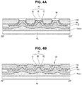
- FIGs. 4A and 4B are schematic cross-sectional views taken along the lines III-III' and IV-IV' of FIG. 3 , respectively.
- the touch pad region has a plurality of open sections (or openings) OP.
- the open section OP is a contact hole that exposes a portion of the pad electrode PE, and the exposed pad electrode PE is electrically connected to a flexible substrate or a circuit board by using a connection element such as a conductive ball.
- the single pad electrode PE may correspond to the plurality of open sections OP. Namely, the pad electrode PE may correspond to two or more contact holes.
- the open section (OP) may have a polygonal shape such as a rectangular shape, pentagonal shape or hexagonal shape.
- a laser lift-off (LLO) process is performed in the step of removing the temporary substrate.
- the heat by the laser, which is applied to the pad electrode PE is more uniformly dissipated in the open section OP of the hexagonal shape than in the open section OP of the rectangular shape.
- a thermal stress to an adjacent element by the open section OP of the hexagonal shape is decreased in comparison to the open section OP of the rectangular shape. Accordingly, the open section OP of the hexagonal shape is preferred.
- the uniformity of heat transfer and heat dissipation can minimize anomalies in the adhesive strength between the pad electrode PE and the temporary substrate during the LLO process such that defects such as tearing of the pad electrode PE can be minimized or prevented.
- the pad electrode PE may have a multi-layered structure including at least one electrode layer.
- the pad electrode PE includes an electrode layer extending from the first touch electrode TX or the second touch electrode RX.
- the pad electrode PE may be electrically connected to the first touch electrode TX or the second touch electrode RX.
- the pad electrode PE may be electrically connected to the first touch electrode TX or the second touch electrode RX by a separate wiring electrode, i.e., the routing line.
- the pad electrode PE includes a first pad electrode BE as a top layer.
- the first pad electrode BE may be disposed to correspond to the open section OP of the protection layer PAC.
- the first pad electrode BE may be disposed to fill the inner side surface of the open section OP in the protection layer PAC according to the arrangement order of the first pad electrode BE and the protection layer PAC. Namely, as shown in FIG. 4A , a center of the first pad electrode BE may correspond to the open section OP in the protection layer PAC to be exposed through the open section OP, and edges of the first pad electrode BE may contact the side surface of the protection layer PAC in the open section OP.
- FIG. 4A a center of the first pad electrode BE may correspond to the open section OP in the protection layer PAC to be exposed through the open section OP, and edges of the first pad electrode BE may contact the side surface of the protection layer PAC in the open section OP.
- FIG. 4A Alternatively, as shown in FIG.
- a center of the first pad electrode BE may correspond to the open section OP in the protection layer PAC to be exposed through the open section OP, and edges of the first pad electrode BE may be covered by the protection layer PAC.
- the protection layer PAC may be disposed between the first pad electrode BE and a second pad electrode TE.
- the pad electrode PE may be an electrode layer including a plurality of electrode layers (sub-layers) as described above.
- the pad electrode PE may include the first pad electrode BE, the second pad electrode TE, which is formed of the same material and disposed on the same layer as the first touch electrode TX, and a third pad electrode RE, which is formed of the same material and disposed on the same layer as the second touch electrode RX.
- the pad electrode PE may have a triple-layered structure.
- the pad electrode PE may have a double-layered structure including the first pad electrode BE and the second pad electrode TE without the third pad electrode RE or the first pad electrode BE and the third pad electrode RE without the second pad electrode TE.
- the required thickness of the pad electrode PE may be provided by forming the pad electrode PE of the same metallic material as the first and second touch electrodes TX and RX in the step of forming the first and second touch electrodes TX and RX.
- a wiring electrode for electrical connection between the pad electrode PE and the touch sensor can be formed at the same time.
- a barrier layer BR is disposed on the protection layer PAC to improve the uniformity of the touch signal.
- the film releasing (or separating) problem may occur in a peripheral region of the substrate.
- a plasma treatment may be performed on the barrier layer BR to prevent the above problem.
- the open section OP in the protection layer PAC may be a reverse-tapered shape with respect to a surface of the adhesive layer AL or the substrate PI of the display substrate DSP.
- the first pad electrode BE is plasma-treated while performing a process of plasma treatment to increase the adhesion strength of the protection layer PAC. Namely, any one layer of the first pad electrode BE may be a plasma-treated electrode layer.
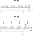
- FIGs. 5A to 5E are schematic cross-sectional views illustrating a manufacturing method of a touch display device according to an embodiment of the present disclosure.
- the explanation of the manufacturing method of the touch display device is focused on a step of forming the pad electrode.
- the touch substrate TSP including the touch sensor is formed using a temporary substrate SUB. Since a glass substrate has an advantage in a laser lift-off (LLO) process using a laser, the temporary substrate SUB may be a glass substrate.
- LLO laser lift-off
- a sacrificial layer SL is disposed (formed) on the glass substrate, and then a protection layer PAC is disposed on the sacrificial layer SL, as shown in FIG. 5A .
- the sacrificial layer SL may be hydrogenated amorphous silicon (a-Si:H) or hydrogenated and doped amorphous silicon (a-Si:H;n+ or a-Si:H;p+).
- the hydrogen of the sacrificial layer SL is combined (connected or bonded) with the silicon of the temporary substrate SUB.
- the combination (connection or the bond) between the hydrogen of the sacrificial layer SL and the silicon of the temporary substrate SUB are cut off such that the separation of the temporary substrate SUB becomes easier.
- the protection layer PAC is disposed on the sacrificial layer SL.
- the protection layer PAC may be an organic insulating layer of photo-acryl.
- a plurality of open sections OP are formed in the protection layer PAC.
- a portion of the sacrificial layer SL is exposed through each open section OP in the protection layer PAC.
- Each open section OP is formed by removing a portion of the protection layer PAC.
- the portion of the protection layer PAC may be removed by a dry-etching process or a wet-etching process.
- the protection layer PAC has a tapered shape with respect to the temporary substrate SUB. Namely, with respect to the temporary substrate SUB, an upper portion of each open section OP has a width (area) greater than a lower portion of the respective opening section OP.
- the first pad electrode BE is disposed on the protection layer PAC.
- the first pad electrode BE may include a single metal layer, such as a molybdenum (Mo) layer or an indium-tin-oxide (ITO) layer, or multiple metal layers, such as Mo/Al or Mo/Al/Mo.
- the first pad electrode BE may be disposed to cover the open section OP in the protection layer PAC.
- the single pad electrode may include a plurality of first pad electrodes BE respectively covering the plurality of open sections OP. The first pad electrodes BE in adjacent open sections OP are spaced apart from each other.
- the first pad electrode BE in the open section OP contacts the portion of the sacrificial layer SL exposed through the open section OP.
- the first pad electrode BE may cover a side surface of the protection layer PAC in the open section OP. Adjacent two first pad electrodes BE are spaced apart from each other in a top surface of the protection layer PAC between adjacent two open sections OP.
- a plasma treatment process is performed on the protection layer PAC to improve an adhesion strength at the interface.
- the first pad electrode BE arranged in the open section OP is also plasma-treated.
- the plasma treatment process is performed using an ionized gas such as argon (Ar), oxygen (O 2 ), hydrogen (H2) and nitrogen (N 2 ).
- the adhesion strength between the barrier layer BR and each of the protection layer PAC and the first pad electrode BE and/or between the second pad electrode TE and the first pad electrode BE are improved by the plasma treatment to the protection layer PAC and/or the first pad electrode BE such that the problem of defects in a flexible environment is minimized or prevented.
- the sacrificial layer SL on the temporary substrate SUB is exposed to the plasma treatment process, there may be a problem in the laser lift-off process of the sacrificial layer SL.
- the plasma treatment is performed after forming the first pad electrode BE, which covers the open section OP, the sacrificial layer SL on the temporary substrate SUB is not exposed to the plasma treatment process such that the problem in the laser lift-off process is prevented.
- the arrangement order of the first pad electrode BE and the protection layer PAC may be changed.
- the protection layer PAC is disposed after the first pad electrode BE is disposed on the sacrificial layer SL.
- the open section OP may be formed in the protection layer PAC by forming a contact hole corresponding to the first pad electrode BE.
- the arrangement order between the first pad electrode BE and the protection layer PAC may be selectively changed.
- the first pad electrode BE may be disposed on the inner surface of the open section OP according to the arrangement order.
- the protection layer PAC is disposed before the first pad electrode BE is disposed, there is an advantage of obtaining a more stable electrical connection characteristic in connection with a circuit board using a conductive ball.
- the protection layer PAC is disposed before the first pad electrode BE is disposed, the electrical connection of the first pad electrode with another electrode, which is disposed by extending from the touch sensor over the first pad electrode BE, can be further improved.
- the barrier layer BR is disposed on the protection layer PAC to improve the uniformity of the touch signal.
- the plasma treatment process is performed onto the protection layer PAC.
- the barrier layer BR may be formed to correspond to an upper surface and a side surface of the protection layer PAC. As a result, in the open section OP, both ends of the first pad electrode BE are covered with the barrier layer BR, and a center of the first pad electrode BE is exposed.
- the barrier layer BR may be omitted.
- first touch electrode TX, the second pad electrode TE, the first insulating layer ILD, the second touch electrode RX and the third pad electrode RE are sequentially formed.
- the first touch electrode TX and the second touch electrode RX are insulated by the first insulating layer ILD in the active area AA, while the second pad electrode TE and the third pad electrode RE contact each other in the touch pad region to form the pad electrode PE.
- the first touch electrode TX and the second pad electrode TE are formed.
- the first touch electrode TX and the second pad electrode TE are formed of the same material and spaced apart from each other.
- the first insulating layer ILD covering the first touch electrode TX and exposing the second pad electrode TE is formed. Edges of the second pad electrode TE may be covered with the first insulating layer ILD.
- the second touch electrode RX corresponding to the first touch electrode TX, is formed on the first insulating layer ILD, and the third pad electrode RE extending from the second touch electrode RX is formed on the second pad electrode TE.
- the pad electrode PE in the opening section OP may have a triple-layered structure including the first to third pad electrodes BE, TE and RE, and the pad electrode PE on the protection layer PAC between adjacent open sections OP may have a double-layered structure including the second and third pad electrodes TE and RE.
- Each of the first touch electrode TX, the second pad electrode TE, the second touch electrode RX and the third pad electrode RE may include a single-layered structure of a metallic material, e.g., Al, AlNd, Mo, MoTi, Cu, or Cr, or a transparent conductive material, e.g., indium-tin-oxide (ITO), indium-zinc-oxide (IZO) or gallium-doped zinc oxide (GZO).
- each of the first touch electrode TX and the second touch electrode RX may include a double-layered structure of a metal layer and a transparent conductive material layer.
- the first and second touch electrodes TX and Rx may be arranged to form a mesh shape.
- the second insulating layer Passi is disposed on the pad electrode PE to protect the pad electrode PE and to provide a planar (or flat) top surface.
- the temporary substrate SUB is removed (separated).
- the touch substrate TSP and the display substrate DSP are attached by an adhesive layer AL.
- the adhesive layer AL may be an epoxy adhesive. Namely, the touch substrate TSP and the display substrate DSP are attached such that the second insulating layer Passi of the touch substrate TSP faces the display substrate DSP.
- a laser is irradiated onto a rear surface of the temporary substrate SUB.
- the hydrogen in amorphous silicon of the sacrificial layer SL is dehydrogenated by the laser such that a surface of the sacrificial layer SL bursts.
- the sacrificial layer SL with the temporary substrate SUB are separated from the protection layer PAC.
- a wet-etching process using an acid solution or the like may be optionally performed to remove a residue of the sacrificial layer SL on the protection layer PAC and the first pad electrode BE.
- the laser in the process of separating the temporary substrate SUB may be a diode pumped solid state (DPSS) laser or an excimer laser.
- DPSS diode pumped solid state
Landscapes
- Engineering & Computer Science (AREA)
- Theoretical Computer Science (AREA)
- General Engineering & Computer Science (AREA)
- Physics & Mathematics (AREA)
- General Physics & Mathematics (AREA)
- Human Computer Interaction (AREA)
- Manufacturing & Machinery (AREA)
- Quality & Reliability (AREA)
- Computer Networks & Wireless Communication (AREA)
- Microelectronics & Electronic Packaging (AREA)
- Devices For Indicating Variable Information By Combining Individual Elements (AREA)
- Position Input By Displaying (AREA)
- Electroluminescent Light Sources (AREA)
- Optics & Photonics (AREA)
Abstract
Description
- This application claims priority to and the benefit of Republic of Korea Patent Application No.
10-2019-00146437 - The present disclosure relates to a touch display device, and more particularly, to a touch display device being capable of minimizing a defect and a manufacturing method of the touch display device.
- A touch sensor is installed in a flat panel display device, e.g., a liquid crystal display (LCD) device, a field emission display (FED) device, a plasma display panel (PDP), an electroluminescent display device or an electrophoretic display device, and is an input device to input predetermined information by user's press or touch while viewing the display device.
- The touch senor for the display devices may be classified into an add-on type touch screen panel (touch sensor), an on-cell type touch screen panel and an integrated type (or an in-cell type) touch screen panel. In the add-on type touch screen panel, after a display panel and a touch screen panel are independently manufactured, the touch screen panel is attached on an upper substrate of the display panel. In the on-cell type touch screen panel, elements (or members) for the touch sensor are formed on a surface of an upper substrate of a display panel. In the integrated type touch sensor, the touch sensor is included inside a display panel.
- Recently, a flexible or foldable touch display device is developed. Particularly, the touch sensor or the touch screen panel is widely applied to an organic light emitting display (OLED) device as the flexible or foldable display device.
- As a touch sensor used for a flexible, bendable, or foldable touch display device, various types of touch sensors, i.e., the add-on type, the on-cell type or the integrated type, can be used. However, since the add-on type touch display device, which is manufactured by attaching the touch panel on the display panel, is relatively thick, it is difficult to realize a flexible or foldable display device.
- On the other hand, the integrated type touch sensor is most frequently used for the flexible or foldable OLED device. However, since an encapsulation layer (or encapsulating film), which includes an organic material and/or an inorganic material, is required in the OLED device to minimize moisture or oxygen penetration, a manufacturing method of the integrated touch OLED device is complicated. In addition, the integrated type touch OLED device may be easily damaged by the bending stress which may occur in a folding operation.
- In the on-cell type touch OLED device, the touch sensor may be disposed or bonded on the encapsulation layer. In addition, the on-cell type touch sensor can be applied to display devices other than the OLED device.
- In a bonding method of the on-cell type touch display device, the touch sensor is electrically connected to a pad region for transmitting and receiving data. The pad region is disposed on the outside, not on the inside, where the touch sensor and the display substrate are bonded. However, defects may occur due to the above-mentioned structure.
- Specifically, in order to manufacture a touch sensor by the bonding method, after the touch sensor is formed using a temporary manufacturing substrate, a step of bonding the touch sensor on the temporary manufacturing substrate with the display panel is performed.
- After the touch sensor disposed on the temporary manufacturing substrate is attached to the display panel, the temporary manufacturing substrate is removed (separated). However, in the manufacturing method of the touch display device, the pad region for transmitting and receiving data of the touch sensor may not be smoothly separated from the temporary manufacturing substrate such that defects may be generated.
- Accordingly, the present disclosure is directed to a touch display device and a manufacturing method of the same that substantially obviate one or more of the problems due to limitations and disadvantages of the related art, and have other advantages.
- Additional features and advantages of the disclosure will be set forth in the description which follows, and in part will be apparent from the description, or may be learned by practice of the disclosure. The objectives and other advantages of the disclosure will be realized and attained by the structure particularly pointed out in the written description and claims hereof as well as the appended drawings.
- To achieve these and other advantages in accordance with the purpose of the embodiments of the present disclosure, as described herein, there is provided a touch display device and a method of manufacturing a touch display device according to the independent claims. Further embodiments are described in the dependent claims. An aspect of the present disclosure is a touch display device comprising: a plurality of light emitting elements; an adhesive layer over the light emitting elements; a first touch electrode and a second touch electrode over the adhesive layer and in an active area; a pad electrode over the adhesive layer and in a touch pad region; and a protection layer over the first touch electrode, the second touch electrode and the pad electrode, wherein the first touch electrode and the second touch electrode are insulated by an insulating layer, and the protection layer includes at least one contact hole corresponding to the pad electrode, and wherein the pad electrode includes a plurality of electrode layers, and one of the plurality of electrode layers extends from the first touch electrode or the second touch electrode.
- In one or more embodiments, a surface of at least one of the plurality of electrode layers is plasma-treated.
- In one or more embodiments, an interface between a first electrode layer of the plurality of electrode layers at an uppermost position and a second electrode layer of the plurality of electrode layers is plasma-treated.
- In one or more embodiments, the at least one contact hole has a pentagonal shape or a hexagonal shape.
- In one or more embodiments, the pad electrode corresponds to two or more contact holes.
- In one or more embodiments, the touch display device further comprises an encapsulation layer between the light emitting elements and the adhesion layer.
- In one or more embodiments, each of the light emitting elements is an organic light emitting diode, and the encapsulation layer covers the organic light emitting diode.
- In one or more embodiments, the protection layer is formed of photo-acryl, and an inner surface of the contact hole has a reverse-tapered shape.
- In one or more embodiments, the pad electrode includes a first pad electrode in the at least one contact hole, a second pad electrode contacting the first pad electrode, and a third pad electrode contacting the second pad electrode.
- In one or more embodiments, the second pad electrode and the third pad electrode are respectively disposed on the same layer as the first touch electrode and the second touch electrode.
- In one or more embodiments, an edge of the first pad electrode covers a side surface of the protection layer in the contact hole.
- In one or more embodiments, the protection layer is disposed between the first pad electrode and the second pad electrode.
- Another aspect of the present disclosure is a method of manufacturing a touch display device comprising: forming a sacrificial layer on a temporary substrate; forming a protection layer including a contact hole in a touch pad region on the sacrificial layer; forming a first pad electrode in the touch pad region; forming a touch electrode on the protection layer and a second pad electrode on the first pad electrode; attaching the temporary substrate and a display substrate; and removing the temporary substrate and the sacrificial layer.
- In one or more embodiments, the method further comprises: performing a plasma treatment to a portion of the protection layer.
- In one or more embodiments, the plasma treatment uses one of an Ar gas plasma, an O2 gas plasma, a H2 gas plasma and a N2 gas plasma.
- In one or more embodiments, a portion of the first pad electrode is plasma-treated in the step of performing the plasma treatment.
- In one or more embodiments, the step of removing the temporary substrate and the sacrificial layer includes irradiating a laser to reduce an adhesion strength of the sacrificial layer.
- In one or more embodiments, a portion of the sacrificial layer is exposed through the contact hole.
- In one or more embodiments, the first pad electrode contacts the portion of the sacrificial layer in the contact hole.
- In one or more embodiments, the step of forming the first pad electrode is prior to the step of forming the protection layer.
- In one or more embodiments, the protection layer covers edges of the first pad electrode.
- In one or more embodiments, the contact hole has a pentagonal shape or a hexagonal shape.
- In one or more embodiments, the method further comprises: forming an insulating layer covering the touch electrode, which is a first touch electrode, and exposing the second pad electrode; and forming a second touch electrode on the insulating layer and a third pad electrode on the second pad electrode, wherein one of the second pad electrode and the third pad electrode is electrically connected to one of the first touch electrode and the second touch electrode.
- In one or more embodiments, the one of the second pad electrode and the third pad electrode extends from the one of the first touch electrode and the second touch electrode.
- It is to be understood that both the foregoing general description and the following detailed description are examples and are explanatory and are intended to provide further explanation of the invention as claimed.
- The accompanying drawings, which are included to provide a further understanding of the disclosure and are incorporated in and constitute a part of this application, illustrate aspect of the disclosure and together with the description serve to explain the principles of the disclosure.
-
FIG. 1 is a schematic plane view of a touch display device according to an embodiment of the present disclosure. -
FIGs. 2A and 2B are schematic cross-sectional views taken along the lines I-I' and II-II' ofFIG. 1 , respectively. -
FIG. 3 is a schematic plan view illustrating a touch pad region of a touch display device according to an embodiment of the present disclosure. -
FIGs. 4A and 4B are schematic cross-sectional views taken along the lines III-III' and IV-IV' ofFIG. 3 , respectively. -
FIGs. 5A to 5E are schematic cross-sectional views illustrating a manufacturing method of a touch display device according to an embodiment of the present disclosure. - As mentioned above, the pad region may be damaged in the on-cell type touch display device. The inventors of the present disclosure have invented a touch display device (or a touch display apparatus) and a manufacturing method of the same being capable of minimizing defects that may occur in the process of manufacturing the touch display device including an on-cell type touch sensor.
- The present disclosure is to provide a touch display device being capable of minimizing defects that may occur in a manufacturing process for a pad region for transmitting and receiving touch-related data.
- The present disclosure is to provide a touch display device being capable of minimizing defect yield in a manufacturing process for a pad region for transmitting and receiving touch signal.
- The object of the present disclosure is not limited to the above-mentioned objects, and other objects will be clearly understood by those skilled in the art from the following description.
- Advantages and technical features of the present disclosure, and methods for achieving the advantages and the technical features will be clarified with reference to embodiments described below in detail together with the accompanying drawings. However, the present disclosure is not limited to the embodiments disclosed below, but will be implemented in various different forms. The embodiments allow the disclosure of the present disclosure to be complete and the ordinary skilled in the art to fully understand. The present disclosure is only defined by the scope of the claims.
- The shapes, sizes, ratios, angles, numbers, etc., disclosed in the drawings for describing the embodiments of the present invention are exemplary, and the present invention is not limited to the drawings. The same reference numerals refer to the same components throughout the specification. In addition, in the description of the present disclosure, when it is determined that detailed descriptions of related known technologies may unnecessarily obscure the subject matter of the present disclosure, detailed descriptions thereof will be omitted. When 'include', 'have', 'consist of', etc., are used in this specification, other parts may be added unless 'only' is used. When a component is expressed as a singular number, the plural number is included unless otherwise specified.
- In interpreting the components, it is interpreted as including an error range even if there is no explicit description.
- In the case of the description of a positional relationship, for example, when a positional relationship of two parts is described as 'on', 'over', 'under', 'at a side', etc., one or more other parts may be positioned between the two parts unless 'right' or 'direct' is used.
- Terms such as 'first', 'second', etc., are used to describe various components, but the components are not limited by these terms. These terms are only used to distinguish one component from another component. Accordingly, the first component mentioned below may be the second component within the technical spirit of the present disclosure.
- Each of features of the various embodiments of the present disclosure may be partially or wholly combined or mixed with each other, and technically various interlocking and driving is possible. Each of the embodiments may be independently implemented with respect to each other or may be implemented together in an association relationship.
- Reference will now be made in detail to aspects of the disclosure, examples of which are illustrated in the accompanying drawings.
-
FIG. 1 is a schematic plane view of a touch display device according to an embodiment of the present disclosure, andFIGs. 2A and 2B are schematic cross-sectional views taken along the lines I-I' and II-II' ofFIG. 1 , respectively. - Referring to
FIGs. 1 ,2A and 2B , atouch display device 100 includes a display substrate DSP and a touch substrate TSP. The display substrate DSP may be an organic light emitting display substrate, but it is not limited thereto. - The display substrate DSP may include a substrate PI, which includes an active area AA and first and second bezel areas BA1 and BA2, a light emitting element LS, which includes an anode, an organic emitting layer and a cathode, over the substrate PI and a thin film transistor (TFT) on the substrate PI for controlling the light emitting element LS according to a driving signal.
- The display substrate DSP and the touch substrate TSP may have a structure that is bonded by an adhesive layer AL, and the adhesive layer AL may be an epoxy-based adhesive layer. The adhesive layer AL may have a structure that is directly adjacent or directly contacts an encapsulation layer ENC of the display substrate DSP and a second insulating layer Passi of the touch substrate TSP.
- The organic emitting layer in the light emitting element LS is vulnerable to oxygen and moisture. Accordingly, the organic emitting layer may be covered by the encapsulation layer ENC to minimize the penetration of oxygen and moisture into the light emitting element LS.
- The encapsulation layer ENC may further include an absorbent or a nano-material for improving the light efficiency of light emitted from the light emitting element LS. In addition, the encapsulation layer ENC may include a plurality of layers, in which an organic material layer and an inorganic material layer are alternately stacked, and may further include various configurations for preventing cracks in order to provide a flexible display device. The explanation to this configuration is omitted.
- The light emitting element LS including the anode, the organic emitting layer, and the cathode is controlled by a circuit unit including the TFT. Electrical signals and current for such control may be supplied through a circuit board connected to a data pad DP.
- The light emitting element LS controls the amount of light, and various wavelengths of light can be emitted through a plurality of light emitting elements LS to display a desired image. The light emitting element (or, each of the light emitting elements) LS may further include a color filter layer.
- The substrate PI of the display substrate DSP may be a polyimide substrate to be used for a flexible display device or a foldable display device and may have a multi-layered structure.
- On the other hand, the display substrate DSP may further include a planarization layer FL for the arrangement of the light emitting elements LS. The planarization layer FL may be made of a material such as photo-acryl and may include a plurality of layers such that the light emitting elements LS, the TFT and the signal lines, e.g., the data lines, which are connected to the TFT, may be disposed on or over the planarization layer FL or between the plurality of layers.
- The data lines may be electrically connected to a data pad DP in the second bezel area BA2. In this instance, the data pad DP may be not covered by the touch substrate TSP for connection with the circuit board.
- On the other hand, the touch substrate TSP may include at least one touch pad region, e.g. touch pad regions TP1 and TP2, to transmit the electrical signal from the touch sensor to the circuit board. The touch pad regions TP1 and TP2 may be disposed in the first bezel area BA1 of the touch substrate TSP.
- The touch substrate TSP has the active area AA and the first bezel area BA1. The touch substrate TSP includes a protection layer PAC, a first insulating layer ILD, the second insulating layer Passi, a first touch electrode TX and a second touch electrode RX.
- Although not shown, each of the first touch electrode TX and the second touch electrode RX constituting the touch sensor may be touch electrodes having a metal mesh shape. The first touch electrode TX and the second touch electrode RX are insulated by the first insulating layer ILD.
- Each of the first touch electrode TX and the second touch electrode RX may be made of a transparent conductive material, e.g., indium-tin-oxide (ITO), indium-zinc-oxide (IZO), or gallium-doped zinc oxide (GZO), or a metallic material, e.g., titanium (Ti), aluminum (Al), copper (Cu), or molybdenum (Mo). Each of the first touch electrode TX and the second touch electrode RX may have a single-layered structure or a multi-layered structure.
- The touch pad regions TP1 and TP2 include at least one pad electrode PE. The pad electrode PE may have a multi-layered structure including at least one metal or conductive material. The protection layer PAC may have an open section for electrical connection with a circuit board.
- The protection layer PAC may have functions of photo-resist (PR) and a passivation layer. For example, the protection layer PAC may be formed of an organic material having low dielectric constant.
- Referring to
FIGs. 2A and 2B , at least one electrode layer of the pad electrode PE may be an electrode formed by extension of the first touch electrode TX or the second touch electrode RX. Namely, one of the first and second touch electrodes TX and RX may extend into one of the touch pad regions TP1 and TP2 and the other one of the first and second touch electrodes TX and RX may extend into the other one of the touch pad regions TP1 and TP2 to form the at least one electrode of the pad electrode PE. As a result, as shown inFIG. 2A , the pad electrode PE in the first touch pad region TP1 is electrically connected to the first touch electrode TX, while the pad electrode PE in the second touch pad region TP2 is electrically connected to the second touch electrode RX. Alternatively, as shown inFIG. 2B , the pad electrode PE in the first touch pad region TP1 is electrically connected to the second touch electrode RX, while the pad electrode PE in the second touch pad region TP2 is electrically connected to the first touch electrode TX. - In
FIGs. 2A and 2B , the pad electrode PE in the first touch pad region TP1 extends from one of the first and second touch electrodes TX and RX, and the pad electrode PE in the second touch pad region TP2 extends from the other one of the first and second touch electrodes TX and RX. Alternatively, the pad electrode PE may be connected to one of the first and second touch electrodes TX and RX by a routing line. - A plurality of first touch electrodes TX and a plurality of second touch electrodes RX are disposed on the touch substrate TSP. Since the first touch electrode TX and the second touch electrode RX cross each other with the first insulating layer ILD interposed therebetween, a mutual capacitance is formed therebetween. Accordingly, when the touch substrate TSP is touched, the mutual capacitance between the first touch electrode TX and the second touch electrode RX is changed. The coordinates of the touch position can be detected by measuring the change of the mutual capacitance.
-
FIG. 3 is a schematic plan view illustrating a touch pad region of a touch display device according to an embodiment of the present disclosure, andFIGs. 4A and 4B are schematic cross-sectional views taken along the lines III-III' and IV-IV' ofFIG. 3 , respectively. - Referring to
FIGs. 3 and4A to 4B , the touch pad region has a plurality of open sections (or openings) OP. The open section OP is a contact hole that exposes a portion of the pad electrode PE, and the exposed pad electrode PE is electrically connected to a flexible substrate or a circuit board by using a connection element such as a conductive ball. - The single pad electrode PE may correspond to the plurality of open sections OP. Namely, the pad electrode PE may correspond to two or more contact holes. The open section (OP) may have a polygonal shape such as a rectangular shape, pentagonal shape or hexagonal shape. As described below, the step of removing the temporary substrate in the manufacturing process of the touch substrate TSP using the temporary substrate is essential. A laser lift-off (LLO) process is performed in the step of removing the temporary substrate.
- In the process of removing the temporary substrate with the LLO process, the heat by the laser, which is applied to the pad electrode PE, is more uniformly dissipated in the open section OP of the hexagonal shape than in the open section OP of the rectangular shape. In addition, a thermal stress to an adjacent element by the open section OP of the hexagonal shape is decreased in comparison to the open section OP of the rectangular shape. Accordingly, the open section OP of the hexagonal shape is preferred.
- The uniformity of heat transfer and heat dissipation can minimize anomalies in the adhesive strength between the pad electrode PE and the temporary substrate during the LLO process such that defects such as tearing of the pad electrode PE can be minimized or prevented.
- Referring to
FIGs. 4A and 4B , the pad electrode PE may have a multi-layered structure including at least one electrode layer. - As mentioned above, the pad electrode PE includes an electrode layer extending from the first touch electrode TX or the second touch electrode RX. The pad electrode PE may be electrically connected to the first touch electrode TX or the second touch electrode RX. Alternatively, the pad electrode PE may be electrically connected to the first touch electrode TX or the second touch electrode RX by a separate wiring electrode, i.e., the routing line.
- The pad electrode PE includes a first pad electrode BE as a top layer. The first pad electrode BE may be disposed to correspond to the open section OP of the protection layer PAC. The first pad electrode BE may be disposed to fill the inner side surface of the open section OP in the protection layer PAC according to the arrangement order of the first pad electrode BE and the protection layer PAC. Namely, as shown in
FIG. 4A , a center of the first pad electrode BE may correspond to the open section OP in the protection layer PAC to be exposed through the open section OP, and edges of the first pad electrode BE may contact the side surface of the protection layer PAC in the open section OP. Alternatively, as shown inFIG. 4B , a center of the first pad electrode BE may correspond to the open section OP in the protection layer PAC to be exposed through the open section OP, and edges of the first pad electrode BE may be covered by the protection layer PAC. The protection layer PAC may be disposed between the first pad electrode BE and a second pad electrode TE. - The pad electrode PE may be an electrode layer including a plurality of electrode layers (sub-layers) as described above. For example, the pad electrode PE may include the first pad electrode BE, the second pad electrode TE, which is formed of the same material and disposed on the same layer as the first touch electrode TX, and a third pad electrode RE, which is formed of the same material and disposed on the same layer as the second touch electrode RX. Namely, the pad electrode PE may have a triple-layered structure. Alternatively, the pad electrode PE may have a double-layered structure including the first pad electrode BE and the second pad electrode TE without the third pad electrode RE or the first pad electrode BE and the third pad electrode RE without the second pad electrode TE. Since the pad electrode PE needs to maintain a certain thickness in the electrical connection using the circuit board and the conductive ball, the required thickness of the pad electrode PE may be provided by forming the pad electrode PE of the same metallic material as the first and second touch electrodes TX and RX in the step of forming the first and second touch electrodes TX and RX. In addition, a wiring electrode for electrical connection between the pad electrode PE and the touch sensor can be formed at the same time.
- A barrier layer BR is disposed on the protection layer PAC to improve the uniformity of the touch signal. When the barrier layer BR is disposed, the film releasing (or separating) problem may occur in a peripheral region of the substrate. A plasma treatment may be performed on the barrier layer BR to prevent the above problem.
- The open section OP in the protection layer PAC may be a reverse-tapered shape with respect to a surface of the adhesive layer AL or the substrate PI of the display substrate DSP.
- The first pad electrode BE is plasma-treated while performing a process of plasma treatment to increase the adhesion strength of the protection layer PAC. Namely, any one layer of the first pad electrode BE may be a plasma-treated electrode layer.
-
FIGs. 5A to 5E are schematic cross-sectional views illustrating a manufacturing method of a touch display device according to an embodiment of the present disclosure. - The explanation of the manufacturing method of the touch display device is focused on a step of forming the pad electrode.
- The touch substrate TSP including the touch sensor is formed using a temporary substrate SUB. Since a glass substrate has an advantage in a laser lift-off (LLO) process using a laser, the temporary substrate SUB may be a glass substrate.
- In a method of manufacturing a touch display device using the glass substrate as the temporary substrate SUB, a sacrificial layer SL is disposed (formed) on the glass substrate, and then a protection layer PAC is disposed on the sacrificial layer SL, as shown in
FIG. 5A . - The sacrificial layer SL may be hydrogenated amorphous silicon (a-Si:H) or hydrogenated and doped amorphous silicon (a-Si:H;n+ or a-Si:H;p+).
- The hydrogen of the sacrificial layer SL is combined (connected or bonded) with the silicon of the temporary substrate SUB. When the laser is irradiated, the combination (connection or the bond) between the hydrogen of the sacrificial layer SL and the silicon of the temporary substrate SUB are cut off such that the separation of the temporary substrate SUB becomes easier.
- The protection layer PAC is disposed on the sacrificial layer SL. For example, the protection layer PAC may be an organic insulating layer of photo-acryl. A plurality of open sections OP are formed in the protection layer PAC. A portion of the sacrificial layer SL is exposed through each open section OP in the protection layer PAC. Each open section OP is formed by removing a portion of the protection layer PAC. For example, the portion of the protection layer PAC may be removed by a dry-etching process or a wet-etching process. The protection layer PAC has a tapered shape with respect to the temporary substrate SUB. Namely, with respect to the temporary substrate SUB, an upper portion of each open section OP has a width (area) greater than a lower portion of the respective opening section OP.
- As shown in
FIG. 5B , the first pad electrode BE is disposed on the protection layer PAC. For example, the first pad electrode BE may include a single metal layer, such as a molybdenum (Mo) layer or an indium-tin-oxide (ITO) layer, or multiple metal layers, such as Mo/Al or Mo/Al/Mo. The first pad electrode BE may be disposed to cover the open section OP in the protection layer PAC. As will be described later, the single pad electrode may include a plurality of first pad electrodes BE respectively covering the plurality of open sections OP. The first pad electrodes BE in adjacent open sections OP are spaced apart from each other. The first pad electrode BE in the open section OP contacts the portion of the sacrificial layer SL exposed through the open section OP. In addition, the first pad electrode BE may cover a side surface of the protection layer PAC in the open section OP. Adjacent two first pad electrodes BE are spaced apart from each other in a top surface of the protection layer PAC between adjacent two open sections OP. - Thereafter, a plasma treatment process is performed on the protection layer PAC to improve an adhesion strength at the interface. In this instance, the first pad electrode BE arranged in the open section OP is also plasma-treated. The plasma treatment process is performed using an ionized gas such as argon (Ar), oxygen (O2), hydrogen (H2) and nitrogen (N2). The adhesion strength between the barrier layer BR and each of the protection layer PAC and the first pad electrode BE and/or between the second pad electrode TE and the first pad electrode BE are improved by the plasma treatment to the protection layer PAC and/or the first pad electrode BE such that the problem of defects in a flexible environment is minimized or prevented. Namely, since a surface of the protection layer PAC and a surface of the first pad electrode BE are plasma-treated, an adhesion strength between the protection layer PAC and the barrier layer BR and an adhesion strength between the first pad electrode BE and the second pad electrode TE are improved. In other words, in a case that the touch substrate TSP and the display substrate DSP are attached, an interface between a lower surface of the first pad electrode BE, which is disposed at an uppermost position, and an upper surface of the second pad electrode TE, which is adjacent to the first pad electrode BE, is plasma-treated.
- When the sacrificial layer SL on the temporary substrate SUB is exposed to the plasma treatment process, there may be a problem in the laser lift-off process of the sacrificial layer SL. However, in the present disclosure, since the plasma treatment is performed after forming the first pad electrode BE, which covers the open section OP, the sacrificial layer SL on the temporary substrate SUB is not exposed to the plasma treatment process such that the problem in the laser lift-off process is prevented.
- In the above-described configuration, the arrangement order of the first pad electrode BE and the protection layer PAC may be changed. In this case, after the first pad electrode BE is disposed on the sacrificial layer SL, the protection layer PAC is disposed. The open section OP may be formed in the protection layer PAC by forming a contact hole corresponding to the first pad electrode BE. By performing the plasma treatment process onto the protection layer PAC and the first pad electrode BE after the protection layer PAC is formed, the same effect can be obtained.
- The arrangement order between the first pad electrode BE and the protection layer PAC may be selectively changed. The first pad electrode BE may be disposed on the inner surface of the open section OP according to the arrangement order. When the first pad electrode BE is disposed before the protection layer PAC is disposed, there is an advantage of obtaining a more stable electrical connection characteristic in connection with a circuit board using a conductive ball. On the other hand, when the protection layer PAC is disposed before the first pad electrode BE is disposed, the electrical connection of the first pad electrode with another electrode, which is disposed by extending from the touch sensor over the first pad electrode BE, can be further improved.
- As shown in
FIG. 5C , the barrier layer BR is disposed on the protection layer PAC to improve the uniformity of the touch signal. In the outer portion (peripheral portion) of the touch substrate TSP, where the barrier layer BR and the sacrificial layer SL directly contact, the releasing (separation) problem of the barrier layer BR from the sacrificial layer SL may occur. In the present disclosure, the plasma treatment process is performed onto the protection layer PAC. - For example, the barrier layer BR may be formed to correspond to an upper surface and a side surface of the protection layer PAC. As a result, in the open section OP, both ends of the first pad electrode BE are covered with the barrier layer BR, and a center of the first pad electrode BE is exposed. The barrier layer BR may be omitted.
- Next, the first touch electrode TX, the second pad electrode TE, the first insulating layer ILD, the second touch electrode RX and the third pad electrode RE are sequentially formed. The first touch electrode TX and the second touch electrode RX are insulated by the first insulating layer ILD in the active area AA, while the second pad electrode TE and the third pad electrode RE contact each other in the touch pad region to form the pad electrode PE.
- In more detail, after the barrier layer BR is formed, the first touch electrode TX and the second pad electrode TE are formed. The first touch electrode TX and the second pad electrode TE are formed of the same material and spaced apart from each other. The second pad electrode TE in the open section OP contacts the first pad electrode BE.
- Next, the first insulating layer ILD covering the first touch electrode TX and exposing the second pad electrode TE is formed. Edges of the second pad electrode TE may be covered with the first insulating layer ILD.
- Next, the second touch electrode RX, corresponding to the first touch electrode TX, is formed on the first insulating layer ILD, and the third pad electrode RE extending from the second touch electrode RX is formed on the second pad electrode TE. The pad electrode PE in the opening section OP may have a triple-layered structure including the first to third pad electrodes BE, TE and RE, and the pad electrode PE on the protection layer PAC between adjacent open sections OP may have a double-layered structure including the second and third pad electrodes TE and RE.
- Each of the first touch electrode TX, the second pad electrode TE, the second touch electrode RX and the third pad electrode RE may include a single-layered structure of a metallic material, e.g., Al, AlNd, Mo, MoTi, Cu, or Cr, or a transparent conductive material, e.g., indium-tin-oxide (ITO), indium-zinc-oxide (IZO) or gallium-doped zinc oxide (GZO). Alternatively, each of the first touch electrode TX and the second touch electrode RX may include a double-layered structure of a metal layer and a transparent conductive material layer. When the first and second touch electrodes TX and RX have the single-layered structure, the first and second touch electrodes TX and Rx may be arranged to form a mesh shape.
- Next, the second insulating layer Passi is disposed on the pad electrode PE to protect the pad electrode PE and to provide a planar (or flat) top surface.
- As shown in
FIGs. 5D and5E , the temporary substrate SUB is removed (separated). - Particularly, as shown in
FIG. 5D , the touch substrate TSP and the display substrate DSP are attached by an adhesive layer AL. The adhesive layer AL may be an epoxy adhesive. Namely, the touch substrate TSP and the display substrate DSP are attached such that the second insulating layer Passi of the touch substrate TSP faces the display substrate DSP. - After the touch substrate TSP and the display substrate DSP are attached, a laser is irradiated onto a rear surface of the temporary substrate SUB. The hydrogen in amorphous silicon of the sacrificial layer SL is dehydrogenated by the laser such that a surface of the sacrificial layer SL bursts. As a result, the sacrificial layer SL with the temporary substrate SUB are separated from the protection layer PAC.
- Next, a wet-etching process using an acid solution or the like may be optionally performed to remove a residue of the sacrificial layer SL on the protection layer PAC and the first pad electrode BE.
- The laser in the process of separating the temporary substrate SUB may be a diode pumped solid state (DPSS) laser or an excimer laser.
- It will be apparent to those skilled in the art that various modifications and variations can be made in the aspects of the disclosure without departing from the scope of the disclosure. Thus, it is intended that the present disclosure covers the modifications and variations of this disclosure provided they come within the scope of the appended claims.
Claims (15)
- A touch display device (100), comprising:a plurality of light emitting elements (LS);an adhesive layer (AL) over the light emitting elements (LS);a first touch electrode (TX) and a second touch electrode (RX) over the adhesive layer (AL) and in an active area (AA);a pad electrode (PE) over the adhesive layer (AL) and in a touch pad region (TP1, TP2); anda protection layer (PAC) over the first touch electrode (TX), the second touch electrode (RX) and the pad electrode (PE),wherein the first touch electrode (TX) and the second touch electrode (RX) are insulated by an insulating layer (ILD), and the protection layer (PAC) includes at least one contact hole (OP) corresponding to the pad electrode (PE), andwherein the pad electrode (PE) includes a plurality of electrode layers, and one of the plurality of electrode layers extends from the first touch electrode (TX) or the second touch electrode (RX).
- The touch display device (100) according to claim 1, wherein a surface of at least one of the plurality of electrode layers is plasma-treated.
- The touch display device (100) according to claim 1 or 2, wherein an interface between a first electrode layer of the plurality of electrode layers at an uppermost position and a second electrode layer of the plurality of electrode layers is plasma-treated.
- The touch display device (100) according to any one of claims 1 to 3, wherein the at least one contact hole (OP) has a pentagonal shape or a hexagonal shape, and the pad electrode (PE) corresponds to two or more contact holes (OP).
- The touch display device (100) according to any one of claims 1 to 4, further comprising an encapsulation layer (ENC) between the light emitting elements (LS) and the adhesion layer (AL),
wherein each of the light emitting elements (LS) is an organic light emitting diode, and the encapsulation layer (ENC) covers the organic light emitting diode. - The touch display device (100) according to any one of claims 1 to 5, wherein the protection layer (PAC) is formed of photo-acryl, and an inner surface of the at least one contact hole (OP) has a reverse-tapered shape.
- The touch display device (100) according to any one of claims 1 to 6, wherein the pad electrode (PE) includes a first pad electrode (BE) in the at least one contact hole (OP), a second pad electrode (TE) contacting the first pad electrode (BE), and a third pad electrode (RE) contacting the second pad electrode (TE), and
wherein the second pad electrode (TE) and the third pad electrode (RE) are respectively disposed on the same layer as the first touch electrode (TX) and the second touch electrode (RX). - The touch display device (100) according to claim 7, wherein an edge of the first pad electrode (BE) covers a side surface of the protection layer (PAC) in the contact hole (OP), or wherein the protection layer (PAC) is disposed between the first pad electrode (BE) and the second pad electrode (TE).
- A method of manufacturing a touch display device (100), comprising:forming a sacrificial layer (SL) on a temporary substrate (SUB);forming a protection layer (PAC) including a contact hole (OP) in a touch pad region (TP1, TP2) on the sacrificial layer (SL);forming a first pad electrode (BE) in the touch pad region;forming a touch electrode on the protection layer (PAC) and a second pad electrode (TE) on the first pad electrode (BE);attaching the temporary substrate (SUB) and a display substrate (DSP); andremoving the temporary substrate (SUB) and the sacrificial layer (SL).
- The method according to claim 9, further comprising: performing a plasma treatment to a portion of the protection layer (PAC),
wherein, preferably, the plasma treatment uses one of an Ar gas plasma, an O2 gas plasma, a H2 gas plasma and a N2 gas plasma, and a portion of the first pad electrode (BE) is plasma-treated in the step of performing the plasma treatment. - The method according to claim 9 or 10, wherein the step of removing the temporary substrate (SUB) and the sacrificial layer (SL) includes irradiating a laser to reduce an adhesion strength of the sacrificial layer (SL).
- The method according to any one of claims 9 to 11, wherein a portion of the sacrificial layer (SL) is exposed through the contact hole (OP),
wherein, preferably, the first pad electrode (BE) contacts the portion of the sacrificial layer (SL) in the contact hole (OP). - The method according to any one of claims 9 or 11, wherein the step of forming the first pad electrode (BE) is prior to the step of forming the protection layer (PAC),
wherein, preferably, the protection layer (PAC) covers edges of the first pad electrode. - The method according to any one of claims 9 to 13, wherein the contact hole (OP) has a pentagonal shape or a hexagonal shape.
- The method according to any one of claims 9 to 14, further comprising:forming an insulating layer (ILD) covering the touch electrode, which is a first touch electrode (TX), and exposing the second pad electrode (TE); andforming a second touch electrode (RX) on the insulating layer (ILD) and a third pad electrode (RE) on the second pad electrode (TE),wherein one of the second pad electrode (TE) and the third pad electrode (RE) is electrically connected to one of the first touch electrode (TX) and the second touch electrode (RX),wherein, preferably, the one of the second pad electrode (EE) and the and third pad electrode (RE) extends from the one of the first touch electrode (TX) and the second touch electrode (RX).
Priority Applications (1)
| Application Number | Priority Date | Filing Date | Title |
|---|---|---|---|
| EP24150873.8A EP4328723A3 (en) | 2019-11-15 | 2020-10-06 | Touch display device and method of manufacturing of the same |
Applications Claiming Priority (1)
| Application Number | Priority Date | Filing Date | Title |
|---|---|---|---|
| KR1020190146437A KR20210059239A (en) | 2019-11-15 | 2019-11-15 | Touch display apparatus and manufacturing method of the same |
Related Child Applications (2)
| Application Number | Title | Priority Date | Filing Date |
|---|---|---|---|
| EP24150873.8A Division-Into EP4328723A3 (en) | 2019-11-15 | 2020-10-06 | Touch display device and method of manufacturing of the same |
| EP24150873.8A Division EP4328723A3 (en) | 2019-11-15 | 2020-10-06 | Touch display device and method of manufacturing of the same |
Publications (2)
| Publication Number | Publication Date |
|---|---|
| EP3822749A1 true EP3822749A1 (en) | 2021-05-19 |
| EP3822749B1 EP3822749B1 (en) | 2024-04-17 |
Family
ID=72752749
Family Applications (2)
| Application Number | Title | Priority Date | Filing Date |
|---|---|---|---|
| EP20200245.7A Active EP3822749B1 (en) | 2019-11-15 | 2020-10-06 | Touch display device and method of manufacturing of the same |
| EP24150873.8A Pending EP4328723A3 (en) | 2019-11-15 | 2020-10-06 | Touch display device and method of manufacturing of the same |
Family Applications After (1)
| Application Number | Title | Priority Date | Filing Date |
|---|---|---|---|
| EP24150873.8A Pending EP4328723A3 (en) | 2019-11-15 | 2020-10-06 | Touch display device and method of manufacturing of the same |
Country Status (6)
| Country | Link |
|---|---|
| US (3) | US11513624B2 (en) |
| EP (2) | EP3822749B1 (en) |
| JP (2) | JP7171670B2 (en) |
| KR (1) | KR20210059239A (en) |
| CN (2) | CN112817472B (en) |
| TW (1) | TWI753596B (en) |
Families Citing this family (2)
| Publication number | Priority date | Publication date | Assignee | Title |
|---|---|---|---|---|
| KR20210059239A (en) | 2019-11-15 | 2021-05-25 | 엘지디스플레이 주식회사 | Touch display apparatus and manufacturing method of the same |
| US12207534B2 (en) * | 2021-12-03 | 2025-01-21 | Wuhan China Star Optoelectronics Semiconductor Display Technology Co., Ltd. | Flexible display panel and manufacturing method thereof |
Citations (2)
| Publication number | Priority date | Publication date | Assignee | Title |
|---|---|---|---|---|
| US20180211082A1 (en) * | 2017-01-23 | 2018-07-26 | Dongwoo Fine-Chem Co., Ltd. | High-performance film-type touch sensor and method of fabricating the same |
| US20180329552A1 (en) * | 2017-05-11 | 2018-11-15 | Lg Display Co., Ltd. | Display device |
Family Cites Families (21)
| Publication number | Priority date | Publication date | Assignee | Title |
|---|---|---|---|---|
| KR101314779B1 (en) * | 2010-08-18 | 2013-10-08 | 엘지디스플레이 주식회사 | Electrostatic capacity type touch screen panel and method of manufacturing the same |
| KR101807849B1 (en) * | 2010-12-08 | 2017-12-12 | 삼성디스플레이 주식회사 | Organinc light emitting display device and manufacturing method for the same |
| JP5836656B2 (en) * | 2011-06-15 | 2015-12-24 | 三菱電機株式会社 | Touch screen, touch panel and display device |
| JP2014021675A (en) * | 2012-07-17 | 2014-02-03 | Fujimori Kogyo Co Ltd | Hard coat film and touch panel using the same |
| KR101341030B1 (en) | 2012-08-29 | 2013-12-13 | 엘지디스플레이 주식회사 | Organic emitting display device and method for manufacturing the same |
| KR102124906B1 (en) * | 2013-12-26 | 2020-07-07 | 엘지디스플레이 주식회사 | Organic electro luminescent device having touch screen and method of fabricationg the same |
| KR102299875B1 (en) * | 2014-11-07 | 2021-09-07 | 엘지디스플레이 주식회사 | Touch panel, method of manufacturing the same and touch panel integrated organic light emitting display device |
| KR102325190B1 (en) * | 2015-04-13 | 2021-11-10 | 삼성디스플레이 주식회사 | Touch panel |
| KR102490624B1 (en) | 2015-10-30 | 2023-01-20 | 엘지디스플레이 주식회사 | Flexible Display and Method for Manufacturing the Same |
| KR102392683B1 (en) * | 2015-11-30 | 2022-05-02 | 엘지디스플레이 주식회사 | Display device with a built-in touch screen |
| JP2017117086A (en) * | 2015-12-22 | 2017-06-29 | 信越ポリマー株式会社 | Conductive sheet for capacitive touch sensor, capacitive touch sensor |
| KR101908982B1 (en) * | 2016-08-31 | 2018-10-17 | 엘지디스플레이 주식회사 | Organic light emitting display with touch sensor and fabricating method thereof |
| KR101926527B1 (en) * | 2016-09-30 | 2018-12-10 | 엘지디스플레이 주식회사 | Organic light emitting display with touch sensor and fabricating method thereof |
| KR20180044640A (en) * | 2016-10-24 | 2018-05-03 | 엘지디스플레이 주식회사 | Touch screen panel, display device with the same, and method of manufacturing the same |
| JP6518384B2 (en) * | 2017-03-06 | 2019-05-22 | 富士フイルム株式会社 | Touch panel, conductive sheet for touch panel, and touch sensor |
| KR102438256B1 (en) * | 2017-06-07 | 2022-08-30 | 엘지디스플레이 주식회사 | Organic Light Emitting Display Device Having a Touch Screen And Method for Manufacturing the Same |
| CN107491233B (en) * | 2017-09-08 | 2020-04-28 | 京东方科技集团股份有限公司 | Color film substrate, display panel and display device |
| KR101842176B1 (en) | 2017-10-27 | 2018-03-26 | 동우 화인켐 주식회사 | Connecting structure for electrode and electric device comprising the same |
| KR102376822B1 (en) | 2017-10-30 | 2022-03-18 | 엘지디스플레이 주식회사 | Display device with integrated touch screen and method for fabricating the same |
| KR20210059239A (en) | 2019-11-15 | 2021-05-25 | 엘지디스플레이 주식회사 | Touch display apparatus and manufacturing method of the same |
| CN112018159B (en) * | 2020-08-27 | 2023-06-02 | 京东方科技集团股份有限公司 | Touch display panel |
-
2019
- 2019-11-15 KR KR1020190146437A patent/KR20210059239A/en not_active Ceased
-
2020
- 2020-09-18 CN CN202010986379.3A patent/CN112817472B/en active Active
- 2020-09-18 CN CN202410235668.8A patent/CN118244917A/en active Pending
- 2020-10-06 EP EP20200245.7A patent/EP3822749B1/en active Active
- 2020-10-06 TW TW109134624A patent/TWI753596B/en active
- 2020-10-06 EP EP24150873.8A patent/EP4328723A3/en active Pending
- 2020-10-21 JP JP2020176497A patent/JP7171670B2/en active Active
- 2020-10-28 US US17/082,605 patent/US11513624B2/en active Active
-
2022
- 2022-10-28 US US17/976,722 patent/US12099669B2/en active Active
- 2022-11-02 JP JP2022176373A patent/JP7491978B2/en active Active
-
2024
- 2024-08-29 US US18/820,251 patent/US12524095B2/en active Active
Patent Citations (2)
| Publication number | Priority date | Publication date | Assignee | Title |
|---|---|---|---|---|
| US20180211082A1 (en) * | 2017-01-23 | 2018-07-26 | Dongwoo Fine-Chem Co., Ltd. | High-performance film-type touch sensor and method of fabricating the same |
| US20180329552A1 (en) * | 2017-05-11 | 2018-11-15 | Lg Display Co., Ltd. | Display device |
Also Published As
| Publication number | Publication date |
|---|---|
| KR20210059239A (en) | 2021-05-25 |
| US20210149513A1 (en) | 2021-05-20 |
| EP3822749B1 (en) | 2024-04-17 |
| US11513624B2 (en) | 2022-11-29 |
| JP2023017900A (en) | 2023-02-07 |
| JP7491978B2 (en) | 2024-05-28 |
| CN112817472B (en) | 2024-03-22 |
| US20240419274A1 (en) | 2024-12-19 |
| TWI753596B (en) | 2022-01-21 |
| EP4328723A3 (en) | 2024-03-20 |
| JP7171670B2 (en) | 2022-11-15 |
| EP4328723A2 (en) | 2024-02-28 |
| US12099669B2 (en) | 2024-09-24 |
| TW202121025A (en) | 2021-06-01 |
| US20230047791A1 (en) | 2023-02-16 |
| US12524095B2 (en) | 2026-01-13 |
| JP2021082270A (en) | 2021-05-27 |
| CN112817472A (en) | 2021-05-18 |
| CN118244917A (en) | 2024-06-25 |
Similar Documents
| Publication | Publication Date | Title |
|---|---|---|
| US12524095B2 (en) | Display device | |
| TWI911726B (en) | Display apparatus | |
| US7936121B2 (en) | Organic light emitting display device | |
| KR102566090B1 (en) | Organic light emitting display device and method of manufacturing the same | |
| KR20140003046A (en) | Touch window and fabricating method of the same, and lcd using the same | |
| CN108735099B (en) | Display device | |
| JP2006337983A (en) | Method for manufacturing flexible display device | |
| JP2014074757A (en) | Manufacturing method of display device | |
| KR20180025052A (en) | Flexible Display Device | |
| CN111162100A (en) | Organic light-emitting display device and method of manufacturing the same | |
| KR102230692B1 (en) | Organic light emitting display device and method of manufacturing the same | |
| KR20250052354A (en) | Display apparatus | |
| US10672854B2 (en) | Display device | |
| US10621893B2 (en) | Display device, manufacturing method for display device, manufacturing apparatus of display device, mounting device, and controller | |
| CN118870851A (en) | Display panel manufacturing method, display panel and display device | |
| CN113421903B (en) | Display substrate and preparation method thereof, display panel, display device | |
| KR20210074061A (en) | Flexible display device | |
| KR20200072177A (en) | A conductive layer and a display panel having the same | |
| KR102931361B1 (en) | Flexible display apparatus | |
| KR102569924B1 (en) | Organic light emitting display panel and fabricating method of the same | |
| KR20260061382A (en) | Touch display apparatus and manufacturing method of the same | |
| KR20210060718A (en) | Display device and method of manufacturing display device | |
| JP2019067654A (en) | Display device | |
| KR20210080811A (en) | Organic light emitting display device | |
| KR20210068708A (en) | Flexible display device |
Legal Events
| Date | Code | Title | Description |
|---|---|---|---|
| PUAI | Public reference made under article 153(3) epc to a published international application that has entered the european phase |
Free format text: ORIGINAL CODE: 0009012 |
|
| STAA | Information on the status of an ep patent application or granted ep patent |
Free format text: STATUS: REQUEST FOR EXAMINATION WAS MADE |
|
| 17P | Request for examination filed |
Effective date: 20201006 |
|
| AK | Designated contracting states |
Kind code of ref document: A1 Designated state(s): AL AT BE BG CH CY CZ DE DK EE ES FI FR GB GR HR HU IE IS IT LI LT LU LV MC MK MT NL NO PL PT RO RS SE SI SK SM TR |
|
| RBV | Designated contracting states (corrected) |
Designated state(s): AL AT BE BG CH CY CZ DE DK EE ES FI FR GB GR HR HU IE IS IT LI LT LU LV MC MK MT NL NO PL PT RO RS SE SI SK SM TR |
|
| STAA | Information on the status of an ep patent application or granted ep patent |
Free format text: STATUS: EXAMINATION IS IN PROGRESS |
|
| 17Q | First examination report despatched |
Effective date: 20220307 |
|
| GRAP | Despatch of communication of intention to grant a patent |
Free format text: ORIGINAL CODE: EPIDOSNIGR1 |
|
| STAA | Information on the status of an ep patent application or granted ep patent |
Free format text: STATUS: GRANT OF PATENT IS INTENDED |
|
| RIC1 | Information provided on ipc code assigned before grant |
Ipc: G06F 3/044 20060101ALI20231010BHEP Ipc: G06F 3/041 20060101AFI20231010BHEP |
|
| INTG | Intention to grant announced |
Effective date: 20231115 |
|
| GRAS | Grant fee paid |
Free format text: ORIGINAL CODE: EPIDOSNIGR3 |
|
| GRAA | (expected) grant |
Free format text: ORIGINAL CODE: 0009210 |
|
| STAA | Information on the status of an ep patent application or granted ep patent |
Free format text: STATUS: THE PATENT HAS BEEN GRANTED |
|
| AK | Designated contracting states |
Kind code of ref document: B1 Designated state(s): AL AT BE BG CH CY CZ DE DK EE ES FI FR GB GR HR HU IE IS IT LI LT LU LV MC MK MT NL NO PL PT RO RS SE SI SK SM TR |
|
| REG | Reference to a national code |
Ref country code: GB Ref legal event code: FG4D |
|
| REG | Reference to a national code |
Ref country code: CH Ref legal event code: EP |
|
| REG | Reference to a national code |
Ref country code: DE Ref legal event code: R096 Ref document number: 602020029064 Country of ref document: DE |
|
| REG | Reference to a national code |
Ref country code: IE Ref legal event code: FG4D |
|
| REG | Reference to a national code |
Ref country code: LT Ref legal event code: MG9D |
|
| REG | Reference to a national code |
Ref country code: NL Ref legal event code: MP Effective date: 20240417 |
|
| REG | Reference to a national code |
Ref country code: AT Ref legal event code: MK05 Ref document number: 1677875 Country of ref document: AT Kind code of ref document: T Effective date: 20240417 |
|
| PG25 | Lapsed in a contracting state [announced via postgrant information from national office to epo] |
Ref country code: NL Free format text: LAPSE BECAUSE OF FAILURE TO SUBMIT A TRANSLATION OF THE DESCRIPTION OR TO PAY THE FEE WITHIN THE PRESCRIBED TIME-LIMIT Effective date: 20240417 |
|
| PG25 | Lapsed in a contracting state [announced via postgrant information from national office to epo] |
Ref country code: NL Free format text: LAPSE BECAUSE OF FAILURE TO SUBMIT A TRANSLATION OF THE DESCRIPTION OR TO PAY THE FEE WITHIN THE PRESCRIBED TIME-LIMIT Effective date: 20240417 |
|
| PG25 | Lapsed in a contracting state [announced via postgrant information from national office to epo] |
Ref country code: IS Free format text: LAPSE BECAUSE OF FAILURE TO SUBMIT A TRANSLATION OF THE DESCRIPTION OR TO PAY THE FEE WITHIN THE PRESCRIBED TIME-LIMIT Effective date: 20240817 |
|
| PG25 | Lapsed in a contracting state [announced via postgrant information from national office to epo] |
Ref country code: BG Free format text: LAPSE BECAUSE OF FAILURE TO SUBMIT A TRANSLATION OF THE DESCRIPTION OR TO PAY THE FEE WITHIN THE PRESCRIBED TIME-LIMIT Effective date: 20240417 |
|
| PG25 | Lapsed in a contracting state [announced via postgrant information from national office to epo] |
Ref country code: FI Free format text: LAPSE BECAUSE OF FAILURE TO SUBMIT A TRANSLATION OF THE DESCRIPTION OR TO PAY THE FEE WITHIN THE PRESCRIBED TIME-LIMIT Effective date: 20240417 Ref country code: HR Free format text: LAPSE BECAUSE OF FAILURE TO SUBMIT A TRANSLATION OF THE DESCRIPTION OR TO PAY THE FEE WITHIN THE PRESCRIBED TIME-LIMIT Effective date: 20240417 |
|
| PG25 | Lapsed in a contracting state [announced via postgrant information from national office to epo] |
Ref country code: GR Free format text: LAPSE BECAUSE OF FAILURE TO SUBMIT A TRANSLATION OF THE DESCRIPTION OR TO PAY THE FEE WITHIN THE PRESCRIBED TIME-LIMIT Effective date: 20240718 |
|
| PG25 | Lapsed in a contracting state [announced via postgrant information from national office to epo] |
Ref country code: PT Free format text: LAPSE BECAUSE OF FAILURE TO SUBMIT A TRANSLATION OF THE DESCRIPTION OR TO PAY THE FEE WITHIN THE PRESCRIBED TIME-LIMIT Effective date: 20240819 |
|
| PG25 | Lapsed in a contracting state [announced via postgrant information from national office to epo] |
Ref country code: ES Free format text: LAPSE BECAUSE OF FAILURE TO SUBMIT A TRANSLATION OF THE DESCRIPTION OR TO PAY THE FEE WITHIN THE PRESCRIBED TIME-LIMIT Effective date: 20240417 |
|
| PG25 | Lapsed in a contracting state [announced via postgrant information from national office to epo] |
Ref country code: AT Free format text: LAPSE BECAUSE OF FAILURE TO SUBMIT A TRANSLATION OF THE DESCRIPTION OR TO PAY THE FEE WITHIN THE PRESCRIBED TIME-LIMIT Effective date: 20240417 |
|
| PG25 | Lapsed in a contracting state [announced via postgrant information from national office to epo] |
Ref country code: PL Free format text: LAPSE BECAUSE OF FAILURE TO SUBMIT A TRANSLATION OF THE DESCRIPTION OR TO PAY THE FEE WITHIN THE PRESCRIBED TIME-LIMIT Effective date: 20240417 |
|
| PG25 | Lapsed in a contracting state [announced via postgrant information from national office to epo] |
Ref country code: LV Free format text: LAPSE BECAUSE OF FAILURE TO SUBMIT A TRANSLATION OF THE DESCRIPTION OR TO PAY THE FEE WITHIN THE PRESCRIBED TIME-LIMIT Effective date: 20240417 |
|
| PG25 | Lapsed in a contracting state [announced via postgrant information from national office to epo] |
Ref country code: PT Free format text: LAPSE BECAUSE OF FAILURE TO SUBMIT A TRANSLATION OF THE DESCRIPTION OR TO PAY THE FEE WITHIN THE PRESCRIBED TIME-LIMIT Effective date: 20240819 Ref country code: PL Free format text: LAPSE BECAUSE OF FAILURE TO SUBMIT A TRANSLATION OF THE DESCRIPTION OR TO PAY THE FEE WITHIN THE PRESCRIBED TIME-LIMIT Effective date: 20240417 Ref country code: NO Free format text: LAPSE BECAUSE OF FAILURE TO SUBMIT A TRANSLATION OF THE DESCRIPTION OR TO PAY THE FEE WITHIN THE PRESCRIBED TIME-LIMIT Effective date: 20240717 Ref country code: LV Free format text: LAPSE BECAUSE OF FAILURE TO SUBMIT A TRANSLATION OF THE DESCRIPTION OR TO PAY THE FEE WITHIN THE PRESCRIBED TIME-LIMIT Effective date: 20240417 Ref country code: IS Free format text: LAPSE BECAUSE OF FAILURE TO SUBMIT A TRANSLATION OF THE DESCRIPTION OR TO PAY THE FEE WITHIN THE PRESCRIBED TIME-LIMIT Effective date: 20240817 Ref country code: HR Free format text: LAPSE BECAUSE OF FAILURE TO SUBMIT A TRANSLATION OF THE DESCRIPTION OR TO PAY THE FEE WITHIN THE PRESCRIBED TIME-LIMIT Effective date: 20240417 Ref country code: GR Free format text: LAPSE BECAUSE OF FAILURE TO SUBMIT A TRANSLATION OF THE DESCRIPTION OR TO PAY THE FEE WITHIN THE PRESCRIBED TIME-LIMIT Effective date: 20240718 Ref country code: FI Free format text: LAPSE BECAUSE OF FAILURE TO SUBMIT A TRANSLATION OF THE DESCRIPTION OR TO PAY THE FEE WITHIN THE PRESCRIBED TIME-LIMIT Effective date: 20240417 Ref country code: ES Free format text: LAPSE BECAUSE OF FAILURE TO SUBMIT A TRANSLATION OF THE DESCRIPTION OR TO PAY THE FEE WITHIN THE PRESCRIBED TIME-LIMIT Effective date: 20240417 Ref country code: BG Free format text: LAPSE BECAUSE OF FAILURE TO SUBMIT A TRANSLATION OF THE DESCRIPTION OR TO PAY THE FEE WITHIN THE PRESCRIBED TIME-LIMIT Effective date: 20240417 Ref country code: AT Free format text: LAPSE BECAUSE OF FAILURE TO SUBMIT A TRANSLATION OF THE DESCRIPTION OR TO PAY THE FEE WITHIN THE PRESCRIBED TIME-LIMIT Effective date: 20240417 Ref country code: RS Free format text: LAPSE BECAUSE OF FAILURE TO SUBMIT A TRANSLATION OF THE DESCRIPTION OR TO PAY THE FEE WITHIN THE PRESCRIBED TIME-LIMIT Effective date: 20240717 |
|
| PG25 | Lapsed in a contracting state [announced via postgrant information from national office to epo] |
Ref country code: DK Free format text: LAPSE BECAUSE OF FAILURE TO SUBMIT A TRANSLATION OF THE DESCRIPTION OR TO PAY THE FEE WITHIN THE PRESCRIBED TIME-LIMIT Effective date: 20240417 |
|
| REG | Reference to a national code |
Ref country code: DE Ref legal event code: R097 Ref document number: 602020029064 Country of ref document: DE |
|
| PG25 | Lapsed in a contracting state [announced via postgrant information from national office to epo] |
Ref country code: EE Free format text: LAPSE BECAUSE OF FAILURE TO SUBMIT A TRANSLATION OF THE DESCRIPTION OR TO PAY THE FEE WITHIN THE PRESCRIBED TIME-LIMIT Effective date: 20240417 |
|
| PG25 | Lapsed in a contracting state [announced via postgrant information from national office to epo] |
Ref country code: CZ Free format text: LAPSE BECAUSE OF FAILURE TO SUBMIT A TRANSLATION OF THE DESCRIPTION OR TO PAY THE FEE WITHIN THE PRESCRIBED TIME-LIMIT Effective date: 20240417 |
|
| PG25 | Lapsed in a contracting state [announced via postgrant information from national office to epo] |
Ref country code: RO Free format text: LAPSE BECAUSE OF FAILURE TO SUBMIT A TRANSLATION OF THE DESCRIPTION OR TO PAY THE FEE WITHIN THE PRESCRIBED TIME-LIMIT Effective date: 20240417 Ref country code: SK Free format text: LAPSE BECAUSE OF FAILURE TO SUBMIT A TRANSLATION OF THE DESCRIPTION OR TO PAY THE FEE WITHIN THE PRESCRIBED TIME-LIMIT Effective date: 20240417 |
|
| PG25 | Lapsed in a contracting state [announced via postgrant information from national office to epo] |
Ref country code: SM Free format text: LAPSE BECAUSE OF FAILURE TO SUBMIT A TRANSLATION OF THE DESCRIPTION OR TO PAY THE FEE WITHIN THE PRESCRIBED TIME-LIMIT Effective date: 20240417 |
|
| PG25 | Lapsed in a contracting state [announced via postgrant information from national office to epo] |
Ref country code: SM Free format text: LAPSE BECAUSE OF FAILURE TO SUBMIT A TRANSLATION OF THE DESCRIPTION OR TO PAY THE FEE WITHIN THE PRESCRIBED TIME-LIMIT Effective date: 20240417 Ref country code: SK Free format text: LAPSE BECAUSE OF FAILURE TO SUBMIT A TRANSLATION OF THE DESCRIPTION OR TO PAY THE FEE WITHIN THE PRESCRIBED TIME-LIMIT Effective date: 20240417 Ref country code: RO Free format text: LAPSE BECAUSE OF FAILURE TO SUBMIT A TRANSLATION OF THE DESCRIPTION OR TO PAY THE FEE WITHIN THE PRESCRIBED TIME-LIMIT Effective date: 20240417 Ref country code: EE Free format text: LAPSE BECAUSE OF FAILURE TO SUBMIT A TRANSLATION OF THE DESCRIPTION OR TO PAY THE FEE WITHIN THE PRESCRIBED TIME-LIMIT Effective date: 20240417 Ref country code: DK Free format text: LAPSE BECAUSE OF FAILURE TO SUBMIT A TRANSLATION OF THE DESCRIPTION OR TO PAY THE FEE WITHIN THE PRESCRIBED TIME-LIMIT Effective date: 20240417 Ref country code: CZ Free format text: LAPSE BECAUSE OF FAILURE TO SUBMIT A TRANSLATION OF THE DESCRIPTION OR TO PAY THE FEE WITHIN THE PRESCRIBED TIME-LIMIT Effective date: 20240417 |
|
| PG25 | Lapsed in a contracting state [announced via postgrant information from national office to epo] |
Ref country code: IT Free format text: LAPSE BECAUSE OF FAILURE TO SUBMIT A TRANSLATION OF THE DESCRIPTION OR TO PAY THE FEE WITHIN THE PRESCRIBED TIME-LIMIT Effective date: 20240417 |
|
| PLBE | No opposition filed within time limit |
Free format text: ORIGINAL CODE: 0009261 |
|
| STAA | Information on the status of an ep patent application or granted ep patent |
Free format text: STATUS: NO OPPOSITION FILED WITHIN TIME LIMIT |
|
| 26N | No opposition filed |
Effective date: 20250120 |
|
| PG25 | Lapsed in a contracting state [announced via postgrant information from national office to epo] |
Ref country code: SI Free format text: LAPSE BECAUSE OF FAILURE TO SUBMIT A TRANSLATION OF THE DESCRIPTION OR TO PAY THE FEE WITHIN THE PRESCRIBED TIME-LIMIT Effective date: 20240417 |
|
| REG | Reference to a national code |
Ref country code: CH Ref legal event code: PL |
|
| PG25 | Lapsed in a contracting state [announced via postgrant information from national office to epo] |
Ref country code: MC Free format text: LAPSE BECAUSE OF FAILURE TO SUBMIT A TRANSLATION OF THE DESCRIPTION OR TO PAY THE FEE WITHIN THE PRESCRIBED TIME-LIMIT Effective date: 20240417 |
|
| PG25 | Lapsed in a contracting state [announced via postgrant information from national office to epo] |
Ref country code: BE Free format text: LAPSE BECAUSE OF NON-PAYMENT OF DUE FEES Effective date: 20241031 Ref country code: LU Free format text: LAPSE BECAUSE OF NON-PAYMENT OF DUE FEES Effective date: 20241006 |
|
| PG25 | Lapsed in a contracting state [announced via postgrant information from national office to epo] |
Ref country code: CH Free format text: LAPSE BECAUSE OF NON-PAYMENT OF DUE FEES Effective date: 20241031 |
|
| REG | Reference to a national code |
Ref country code: BE Ref legal event code: MM Effective date: 20241031 |
|
| PG25 | Lapsed in a contracting state [announced via postgrant information from national office to epo] |
Ref country code: SE Free format text: LAPSE BECAUSE OF FAILURE TO SUBMIT A TRANSLATION OF THE DESCRIPTION OR TO PAY THE FEE WITHIN THE PRESCRIBED TIME-LIMIT Effective date: 20240417 |
|
| PGFP | Annual fee paid to national office [announced via postgrant information from national office to epo] |
Ref country code: GB Payment date: 20250820 Year of fee payment: 6 |
|
| PGFP | Annual fee paid to national office [announced via postgrant information from national office to epo] |
Ref country code: FR Payment date: 20250821 Year of fee payment: 6 |
|
| PG25 | Lapsed in a contracting state [announced via postgrant information from national office to epo] |
Ref country code: IE Free format text: LAPSE BECAUSE OF NON-PAYMENT OF DUE FEES Effective date: 20241006 |
|
| PGFP | Annual fee paid to national office [announced via postgrant information from national office to epo] |
Ref country code: DE Payment date: 20250820 Year of fee payment: 6 |
|
| PG25 | Lapsed in a contracting state [announced via postgrant information from national office to epo] |
Ref country code: CY Free format text: LAPSE BECAUSE OF FAILURE TO SUBMIT A TRANSLATION OF THE DESCRIPTION OR TO PAY THE FEE WITHIN THE PRESCRIBED TIME-LIMIT; INVALID AB INITIO Effective date: 20201006 |
|
| PG25 | Lapsed in a contracting state [announced via postgrant information from national office to epo] |
Ref country code: HU Free format text: LAPSE BECAUSE OF FAILURE TO SUBMIT A TRANSLATION OF THE DESCRIPTION OR TO PAY THE FEE WITHIN THE PRESCRIBED TIME-LIMIT; INVALID AB INITIO Effective date: 20201006 |