EP3817138B1 - Antenna - Google Patents
Antenna Download PDFInfo
- Publication number
- EP3817138B1 EP3817138B1 EP20193677.0A EP20193677A EP3817138B1 EP 3817138 B1 EP3817138 B1 EP 3817138B1 EP 20193677 A EP20193677 A EP 20193677A EP 3817138 B1 EP3817138 B1 EP 3817138B1
- Authority
- EP
- European Patent Office
- Prior art keywords
- conductor
- end portion
- antenna
- split ring
- stub
- Prior art date
- Legal status (The legal status is an assumption and is not a legal conclusion. Google has not performed a legal analysis and makes no representation as to the accuracy of the status listed.)
- Active
Links
- 239000004020 conductor Substances 0.000 claims description 371
- 230000005855 radiation Effects 0.000 claims description 15
- 239000003990 capacitor Substances 0.000 claims description 11
- 230000005540 biological transmission Effects 0.000 claims description 5
- 239000002184 metal Substances 0.000 description 7
- 230000008878 coupling Effects 0.000 description 2
- 238000010168 coupling process Methods 0.000 description 2
- 238000005859 coupling reaction Methods 0.000 description 2
- 238000010586 diagram Methods 0.000 description 2
- 239000000463 material Substances 0.000 description 2
- 238000000034 method Methods 0.000 description 2
- 239000011347 resin Substances 0.000 description 2
- 229920005989 resin Polymers 0.000 description 2
- 238000004891 communication Methods 0.000 description 1
- 230000001939 inductive effect Effects 0.000 description 1
- 238000012986 modification Methods 0.000 description 1
- 230000004048 modification Effects 0.000 description 1
- 238000007747 plating Methods 0.000 description 1
- 238000005476 soldering Methods 0.000 description 1
- 239000000758 substrate Substances 0.000 description 1
Images


Classifications
-
- H—ELECTRICITY
- H01—ELECTRIC ELEMENTS
- H01Q—ANTENNAS, i.e. RADIO AERIALS
- H01Q7/00—Loop antennas with a substantially uniform current distribution around the loop and having a directional radiation pattern in a plane perpendicular to the plane of the loop
-
- H—ELECTRICITY
- H01—ELECTRIC ELEMENTS
- H01Q—ANTENNAS, i.e. RADIO AERIALS
- H01Q9/00—Electrically-short antennas having dimensions not more than twice the operating wavelength and consisting of conductive active radiating elements
- H01Q9/04—Resonant antennas
- H01Q9/0485—Dielectric resonator antennas
-
- H—ELECTRICITY
- H01—ELECTRIC ELEMENTS
- H01Q—ANTENNAS, i.e. RADIO AERIALS
- H01Q9/00—Electrically-short antennas having dimensions not more than twice the operating wavelength and consisting of conductive active radiating elements
- H01Q9/04—Resonant antennas
- H01Q9/0407—Substantially flat resonant element parallel to ground plane, e.g. patch antenna
-
- H—ELECTRICITY
- H01—ELECTRIC ELEMENTS
- H01Q—ANTENNAS, i.e. RADIO AERIALS
- H01Q5/00—Arrangements for simultaneous operation of antennas on two or more different wavebands, e.g. dual-band or multi-band arrangements
- H01Q5/10—Resonant antennas
-
- H—ELECTRICITY
- H01—ELECTRIC ELEMENTS
- H01Q—ANTENNAS, i.e. RADIO AERIALS
- H01Q1/00—Details of, or arrangements associated with, antennas
- H01Q1/36—Structural form of radiating elements, e.g. cone, spiral, umbrella; Particular materials used therewith
-
- H—ELECTRICITY
- H01—ELECTRIC ELEMENTS
- H01Q—ANTENNAS, i.e. RADIO AERIALS
- H01Q1/00—Details of, or arrangements associated with, antennas
- H01Q1/44—Details of, or arrangements associated with, antennas using equipment having another main function to serve additionally as an antenna, e.g. means for giving an antenna an aesthetic aspect
- H01Q1/46—Electric supply lines or communication lines
-
- H—ELECTRICITY
- H01—ELECTRIC ELEMENTS
- H01Q—ANTENNAS, i.e. RADIO AERIALS
- H01Q1/00—Details of, or arrangements associated with, antennas
- H01Q1/50—Structural association of antennas with earthing switches, lead-in devices or lightning protectors
-
- H—ELECTRICITY
- H01—ELECTRIC ELEMENTS
- H01Q—ANTENNAS, i.e. RADIO AERIALS
- H01Q5/00—Arrangements for simultaneous operation of antennas on two or more different wavebands, e.g. dual-band or multi-band arrangements
- H01Q5/30—Arrangements for providing operation on different wavebands
- H01Q5/307—Individual or coupled radiating elements, each element being fed in an unspecified way
- H01Q5/314—Individual or coupled radiating elements, each element being fed in an unspecified way using frequency dependent circuits or components, e.g. trap circuits or capacitors
- H01Q5/321—Individual or coupled radiating elements, each element being fed in an unspecified way using frequency dependent circuits or components, e.g. trap circuits or capacitors within a radiating element or between connected radiating elements
Landscapes
- Waveguide Aerials (AREA)
- Control Of Motors That Do Not Use Commutators (AREA)
- Details Of Aerials (AREA)
Description
- This invention relates to an antenna.
-
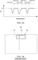
JP 6020451 B Fig. 24 , anantenna 90 has asplit ring resonator 96 using asplit ring 94 which is a ring-shaped conductor with a split or asplit portion 92. - The
antenna 90 ofPatent Document 1 can resonate at one operating frequency but not meet multiband. -
EP 3 001 503 A1 discloses an antenna according to the preamble ofclaim 1. -
WO 2013/027824 A1 discloses an antenna according to the preamble of claim 2. -
JP 2015 185910 A -
WO 2015/029383 A1 discloses an antenna device including a split ring resonance unit, and an impedance matching unit, a power-feeding unit, and a coupling unit, each of which being connected to the split resonance unit. The coupling unit and a metal section in the chassis are joined together, and the antenna device is mounted between a first edge section and a second edge section of the metal section finite distances away from the first edge section and the second edge section. The first edge section and the second edge section face each other. -
US 2006/279464 A1 discloses a dual-band antenna for radiating electromagnetic signals of different frequencies including a ground portion, a feeding part, a body and a shorting part. The feeding part is for feeding signals. The body includes a first radiating part and a second radiating part. The first radiating part includes a bent portion, a first free end, and a first connecting end. The bent portion is between the first free end and the first connecting end. The first connecting end is electronically connected to the feeding part. The second radiating part includes a second connecting end and a second free end. The second connecting end is connected to the first connecting end. The shorting part is between the body and the ground portion - It is an object of the present invention to provide an antenna having a structure which can resonate at a plurality of operating frequencies.
- The above mentioned object is achieved by the antenna according to one of
claims 1 to 4. - By combining an antenna having a split ring resonator with a first conductor and a second conductor which form, at least in part, an open stub or a short stub which has a predetermined electrical length, it is possible to provide an antenna which is small and has a plurality of operating frequencies.
- An appreciation of the objectives of the present invention and a more complete understanding of its structure may be had by studying the following description of the preferred embodiment and by referring to the accompanying drawings.
-
-
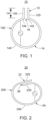
Fig. 1 is a diagram showing a basic structure of an antenna of the present invention. -
Fig. 2 is a diagram showing a modified example of the basic structure of the antenna of the present invention. -
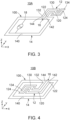
Fig. 3 is a schematic view showing an antenna according to a first embodiment of the present invention. -
Fig. 4 is a schematic view showing a first modified example of the antenna according to the first embodiment of the present invention. A feeding portion is not shown. -
Fig. 5 is a schematic view showing a second modified example of the antenna according to the first embodiment of the present invention. A feeding portion is not shown. -
Fig. 6 is a schematic view showing an antenna according to a second embodiment of the present invention. -
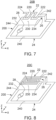
Fig. 7 is a schematic view showing a first modified example of the antenna according to the second embodiment of the present invention. -
Fig. 8 is a schematic view showing a second modified example of the antenna according to the second embodiment of the present invention. -
Fig. 9 is a schematic view showing a third modified example of the antenna according to the second embodiment of the present invention. -
Fig. 10 is a schematic view showing a fourth modified example of the antenna according to the second embodiment of the present invention. -
Fig. 11 is a schematic view showing a fifth modified example of the antenna according to the second embodiment of the present invention. A feeding portion is not shown. -
Fig. 12 is a schematic view showing a sixth modified example of the antenna according to the second embodiment of the present invention. A feeding portion is not shown. -
Fig. 13 is a schematic view showing a seventh modified example of the antenna according to the second embodiment of the present invention. A feeding portion is not shown. -
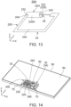
Fig. 14 is a perspective view showing an antenna device including an antenna according to a third embodiment of the present invention. -
Fig. 15 is a perspective view showing the antenna included in the antenna device ofFig. 14 . -
Fig. 16 is a top view showing the antenna ofFig. 15 . -
Fig. 17 is a bottom view showing the antenna ofFig. 15 . -
Fig. 18 is a front view showing the antenna ofFig. 15 . -
Fig. 19 is a rear view showing the antenna ofFig. 15 . -
Fig. 20 is a right-side view showing the antenna ofFig. 15 . -
Fig. 21 is a left-side view showing the antenna ofFig. 15 . -
Fig. 22 is a perspective view showing a modified example of the antenna according to the third embodiment of the present invention. -
Fig. 23 is a graph showing relationship between frequencies supplied to the antenna ofFig. 1 and reflection coefficients S11. Frequency bands at which a stub operates capacitively are represented by "capacitive". Other frequency bands at which the stub operates inductively are represented by "inductive". -
Fig. 24 is a top view showing an antenna disclosed inPatent Document 1. - While the invention is susceptible to various modifications and alternative forms, specific embodiments thereof are shown by way of example in the drawings and will herein be described in detail. It should be understood, however, that the drawings and detailed description thereto are not intended to limit the invention to the particular form disclosed, but on the contrary, the intention is to limit the and scope of the present invention as defined by the appended claims.
- First, referring to
Fig. 1 , the description will be made about a basic structure of an antenna according to the present invention. Anantenna 10 ofFig. 1 is provided with astub 12 and asplit ring 14. Thestub 12 is formed of a pair of conductors, afirst conductor 120 and asecond conductor 130, arranged apart from and in parallel with each other. Thesplit ring 14 is formed of a ring-shaped conductor, or athird conductor 140, with a split or asplit portion 16. Thefirst conductor 120 and thesecond conductor 130 are connected to afirst end portion 142 of thethird conductor 140 and asecond end portion 144 of thethird conductor 140, respectively. - As understood from
Fig. 1 , thethird conductor 140 has a ring shape and forms an inductor. Moreover, the end portions of thethird conductor 140, i.e. thefirst end portion 142 and thesecond end portion 144, are apart from and face each other to form a capacitor. Additionally, in the present specification, the word "ring shape" has a wide meaning including "circular frame shape", "ellipse or oval frame shape" and "polygonal frame shape". - As shown in
Fig. 1 , thefirst conductor 120 and the second conductor 130 (the stub 12) have an electrical length Le. The electrical length Le is a predetermined electrical length which is a length equal to or longer than a necessary length necessary for thefirst conductor 120 and thesecond conductor 130 to form a distributed parameter line at a predetermined frequency band. In other words, thefirst conductor 120 and thesecond conductor 130 form a transmission line having the predetermined electrical length. Since thestub 12 has the predetermined electrical length, it operates inductively or capacitively according to a frequency of an input power. - As understood from
Fig. 1 , thestub 12 and thesplit ring 14 as a whole form asplit ring resonator 100. Thesplit ring resonator 100 operates as an LC resonator which is formed of a capacitor formed of thestub 12, another capacitor formed of thesplit ring 14 and an inductor formed of thesplit ring 14. Since thestub 12 operates inductively or capacitively in accordance with the frequency supplied to thethird conductor 140, thesplit ring resonator 100 can have a plurality of resonance frequencies. In detail, as understood fromFig. 23 , thesplit ring resonator 100 causes LC resonance at frequencies at which thestub 12 becomes capacitive. There is a plurality of frequencies each of which makes thestub 12 capacitive. An operating frequency band of thesplit ring resonator 100 is a frequency band which includes the frequency at which thesplit ring resonator 100 resonates and which has a reflection coefficient S11 smaller than a predetermined value. Thus, thesplit ring resonator 100 has a plurality of operating frequencies. In other words, theantenna 10 has the plurality of operating frequencies. One of the operating frequencies is a low frequency at which thestub 12 has no significant electrical length and thesplit ring resonator 100 causes the LC resonance. Another one of the operating frequencies is an operating frequency corresponding to the electrical length of thestub 12. - In the
antenna 10 ofFig.1 , thestub 12 and thesplit ring 14 can be distinguished from each other. However, thestub 12 and thesplit ring 14 may have a part shared by them. For example, in anantenna 20 shown inFig. 2 , asecond conductor 230 forms astub 22 together with afirst conductor 220. At the same time, thesecond conductor 230 forms asplit ring 24 with asplit portion 26 together with athird conductor 240. Then, thestub 22 and thesplit ring 24 form asplit ring resonator 200. As just described, at least one of thefirst conductor 220 and thesecond conductor 230 may form a part of thesplit ring 24. With this structure, theantenna 20 has a plurality of operating frequencies as with theantenna 10. In addition, since thesecond conductor 230 serves as both of a part of thestub 22 and a part of thesplit ring 24, theantenna 20 can be downsized in comparison with theantenna 10. - In the structure shown in
Fig. 1 or 2 , thestub first conductor second conductor first conductor second conductor first conductor second conductor - Referring to
Fig. 3 , anantenna 10A according to a first embodiment of the present invention has the same structure as theantenna 10 shown inFig. 1 . In other words, theantenna 10A is provided with thestub 12 and thesplit ring 14. In detail, theantenna 10A is provided with thefirst conductor 120, thesecond conductor 130 and thethird conductor 140 which are arranged on the same plane. Materials of thefirst conductor 120, thesecond conductor 130 and thethird conductor 140 are not particularly limited, provided that they are conductive materials. For example, each of thefirst conductor 120, thesecond conductor 130 and thethird conductor 140 may be made of a metal plate. Alternatively, each of thefirst conductor 120, thesecond conductor 130 and thethird conductor 140 may be made of a conductive film included in a circuit board. Moreover, thefirst conductor 120, thesecond conductor 130 and thethird conductor 140 may be separate members or a single member in which they are united. - As shown in
Fig. 3 , each of thefirst conductor 120, thesecond conductor 130 and thethird conductor 140 has afirst end portion second end portion first end portion 122 of thefirst conductor 120 is connected to thefirst end portion 142 of thethird conductor 140. Thefirst end portion 132 of thesecond conductor 130 is connected to thesecond end portion 144 of thethird conductor 140. - As shown in
Fig. 3 , each of thefirst conductor 120 and thesecond conductor 130 has a shape with a plurality of elbow portions. Thefirst conductor 120 and thesecond conductor 130 are juxtaposed with a predetermined interval therebetween to form thestub 12. In the present embodiment, thestub 12 is an open stub. In other words, both of thesecond end portion 124 of thefirst conductor 120 and thesecond end portion 134 of thesecond conductor 130 are open ends. Thestub 12 has a predetermined electrical length. The predetermined electrical length is equal to or longer than a half of a wavelength (= 0.5λ, λ: wavelength) corresponding to one of operation frequencies of theantenna 10A. In other words, the predetermined electrical length is equal to or more than 0.5 times a wavelength of any one of the operating frequencies. In the present embodiment, the electrical length of thestub 12 depends on an electrical length from thefirst end portion 122 of thefirst conductor 120 to thesecond end portion 124 of thefirst conductor 120 or on an electrical length from thefirst end portion 132 of thesecond conductor 130 to thesecond end portion 134 of thesecond conductor 130. - As shown in
Fig. 3 , thethird conductor 140 forms thesplit ring 14 having a rectangular shape. Thefirst end portion 142 of thethird conductor 140 and thesecond end portion 144 of thethird conductor 140 are located apart from each other and form thesplit portion 16 of thesplit ring 14. Thethird conductor 140 is provided with a feedingportion 18. Thestub 12 works inductively or capacitively according to a frequency supplied thereto. Accordingly, thesplit ring resonator 100 formed of thestub 12 and thesplit ring 14 can have a plurality of resonance frequencies. Thus, theantenna 10A can have a plurality of operating frequencies. - In the
antenna 10A shown inFig. 3 , thestub 12 is formed on the same plane as thesplit ring 14 and located outward of thesplit ring 14. However, the present invention is not limited thereto. As in anantenna 10B shown inFig. 4 , thefirst conductor 120 and thesecond conductor 130 which form thestub 12 may be provided inside thesplit ring 14. With this structure, theantenna 10B can be downsized in comparison with theantenna 10A. - In each of the
antenna 10A shown inFig. 3 and theantenna 10B shown inFig. 4 , thestub 12 is formed as the open stub. However, the present invention is not limited thereto. Thestub 12 may be formed as a short stub. For example, as in anantenna 10C shown inFig. 5 , by connecting thesecond end portion 124 of thefirst conductor 120 and thesecond end portion 134 of thesecond conductor 130 to each other by means of afourth conductor 150, astub 12C can be formed as a short stub. However, the present invention is not limited thereto. In order to form the short stub, thefirst conductor 120 and thesecond conductor 130 should be connected to each other by means of thefourth conductor 150 at a position which is apart from thefirst end portion 142 of thethird conductor 140 and thesecond end portion 144 of thethird conductor 140. The electrical length of thestub 12C which is the short stub depends on the electrical length of thefirst conductor 120 or the electrical length of thesecond conductor 130. In addition, the electrical length (the predetermined electrical length) of thestub 12C is equal to or longer than three fourths of a wavelength (= 0.75λ) corresponding to one of the operating frequencies. In other words, the predetermined electrical length is equal to or more than 0.75 times a wavelength of any one of the operating frequencies. - Referring to
Fig. 6 , anantenna 20A according to a second embodiment of the present invention has the same structure as theantenna 20 shown inFig. 2 . In other words, theantenna 20A is provided with thestub 22 and thesplit ring 24. In detail, theantenna 20A ofFig. 6 is provided with thefirst conductor 220, thesecond conductor 230 and thethird conductor 240. Materials of thefirst conductor 220, thesecond conductor 230 and thethird conductor 240 are not particularly limited, provided that they are conductive materials. Each of thefirst conductor 220, thesecond conductor 230 and thethird conductor 240 may be formed of a metal plate. Alternatively, thefirst conductor 220, thesecond conductor 230 and thethird conductor 240 may be formed of a plurality of conductive layers and vias included in a multilayer wiring substrate. Moreover, thefirst conductor 220, thesecond conductor 230 and thethird conductor 240 may be formed as separate members or a single member in which they are united. - As shown in
Fig. 6 , each of thefirst conductor 220, thesecond conductor 230 and thethird conductor 240 has afirst end portion second end portion first end portion 222 of thefirst conductor 220 is connected to thefirst end portion 242 of thethird conductor 240. Thefirst end portion 232 of thesecond conductor 230 is connected to thesecond end portion 244 of thethird conductor 240. - As shown in
Fig. 6 , each of thefirst conductor 220 and thesecond conductor 230 has a rectangular shape long in a lateral direction. Thefirst conductor 220 extends from thefirst end portion 222 thereof in a first lateral direction, and thesecond conductor 230 extends from thefirst end portion 232 thereof in a second lateral direction. Thefirst conductor 220 and thesecond conductor 230 are arranged apart from each other in an up-down direction and in parallel with each other. In other words, thefirst conductor 220 and thesecond conductor 230 are apart from and face each other. In the up-down direction, thefirst conductor 220 is located upward of thesecond conductor 230. Thus, thefirst conductor 220 and thesecond conductor 230 form thestub 22. Theantenna 20A of the present embodiment can reduce a footprint thereof since thestub 22 is formed three-dimensionally. In the present embodiment, the lateral direction is an X-direction. A negative X-direction is the first lateral direction while a positive X-direction is the second lateral direction. Moreover, in the present embodiment, the up-down direction is a Z-direction. A positive Z-direction is directed upward while a negative Z-direction is directed downward. - As understood from
Fig. 6 , in the present embodiment, thestub 22 is an open stub. In other word, each of thesecond end portion 224 of thefirst conductor 220 and thesecond end portion 234 of thesecond conductor 230 is an open end. Thestub 22 has the electrical length Le depending on a length of thefirst conductor 220 or a length of thesecond conductor 230 in the lateral direction. The electrical length (the predetermined electrical length) Le is equal to or longer than a half of a wavelength (= 0.5λ) corresponding one of operating frequencies of theantenna 20A. - As understood from
Fig.6 , thesecond conductor 230 and thethird conductor 240 form thesplit ring 24 having a rectangular shape. Thethird conductor 240 has two elbow portions so that thefirst end portion 242 is located upward of thesecond end portion 244 in the up-down direction. - As shown in
Fig. 6 , thesecond end portion 234 of thesecond conductor 230 and thefirst end portion 242 of thethird conductor 240 are located apart from each other and form thesplit portion 26 in thesplit ring 24. Thesecond conductor 230 is provided with a feedingportion 28. Thestub 22 works inductively or capacitively according to a frequency supplied thereto. Accordingly, thesplit ring resonator 200 formed of thestub 22 and thesplit ring 24 can have a plurality of resonance frequencies. Thus, theantenna 20A can have a plurality of operating frequencies. - In the
antenna 20A shown inFig. 6 , the feedingportion 28 is provided on thesecond conductor 230. However, the present invention is not limited thereto. The feedingportion 28 may be provided on thethird conductor 240 according to a shape and a size of each of thefirst conductor 220, thesecond conductor 230 and thethird conductor 240 and to an arrangement of them (seeFig. 2 ). In other words, in the antenna of this invention, the feedingportion 28 may be provided to either thesecond conductor 230 or thethird conductor 240. Alternatively, the feedingportion 28 may be provided on thefirst conductor 220. In that case, it should be noted that a function of thefirst conductor 220 and a function of thesecond conductor 230 are changed to each other. - In the
antenna 20A shown inFig. 6 , each of thefirst conductor 220 and thesecond conductor 230 has a rectangular shape long in the lateral direction. However, the present invention is not limited thereto. As in anantenna 20B shown inFig. 7 , thefirst conductor 220 may be formed into a meandering shape, and thesecond conductor 230 may be formed into a plane shape. To the contrary, thefirst conductor 220 may be formed into a plane shape, and thesecond conductor 230 may be formed into a meandering shape. Moreover, as in anantenna 20C shown inFig. 8 , thefirst conductor 220 may be formed into a spiral shape, and thesecond conductor 230 may be a plane shape. To the contrary, thefirst conductor 220 may be formed into a plane shape, and thesecond conductor 230 may be formed into a spiral shape. According to these structures, an electrical length of thestub 22 can be lengthen while upsizing of theantenna stub 22 depends on an electrical length of thefirst conductor 220 having the meandering or spiral shape or an electrical length of thesecond conductor 230 having the meandering or spiral shape. - In each of the
antennas Figs. 6 to 8 , thestub 22 is formed as the open stub. However, the present invention is not limited thereto. Thestub 22 may be formed as a short stub. For example, as in each of anantenna 20D shown inFig. 9 and anantenna 20E shown inFig. 10 , by connecting thesecond end portion 224 of thefirst conductor 220 and thesecond conductor 230 to each other by means of afourth conductor 250, astub fourth conductor 250 on thefirst conductor 220 is not limited at thesecond end portion 224 but may be at the vicinity of thesecond end portion 224. By changing the connecting position of thefourth conductor 250, operating frequencies of theantenna fourth conductor 250 which connects thefirst conductor 220 and thesecond conductor 230 to each other at thesecond end portion 224 of thefirst conductor 220 or at the vicinity of thesecond end portion 224. The electrical length of thestub first conductor 220 having the meandering or spiral shape. The electrical length of thestub - In each of the
antennas stub antenna 20F shown inFig. 11 , astub 22F may be formed two-dimensionally. In theantenna 20F ofFig. 11 , thefirst conductor 220 is disposed along an edge of thesecond conductor 230 with a predetermined interval therebetween. Thefirst conductor 220 is formed to have a narrow width, and thesecond conductor 230 is formed to have a wide width. Thefirst end portion 242 of thethird conductor 240 has a width corresponding to the width of thefirst conductor 220. Theantenna 20F having this structure also can have a plurality of operating frequencies. - Each of the
antenna Figs. 6 to 11 , thestub first conductor 220 and thesecond conductor 230. However, the present invention is not limited thereto. Thestub 22 may be formed of three or more conductors. For example, as in anantenna 20G shown inFig.12 , an additionalsecond conductor 230G arranged in parallel with thesecond conductor 230 may be provided. The additionalsecond conductor 230G has the same shape and the same size as thesecond conductor 230. The additionalsecond conductor 230G is connected to thesecond end portion 244 of thethird conductor 240 by means of aconnection portion 231. In the up-down direction, thefirst conductor 220 is located between thesecond conductor 230 and the additionalsecond conductor 230G. In the up-down direction, a distance from thefirst conductor 220 to thesecond conductor 230 is equal to a distance from thefirst conductor 220 to the additionalsecond conductor 230G. Theantenna 20G having this structure can also have a plurality of operating frequencies. - In each of the
antenna first conductor 220 and thesecond conductor 230 has the plane shape. However, the present invention is not limited thereto. For example, as in anantenna 20H shown inFig.13 , astub 22H may be formed by means of asecond conductor 230H having a cylindrical shape. Theantenna 20H having this structure can also have a plurality of operating frequencies. - Referring to
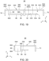
Fig. 14 , anantenna 30 according to a third embodiment of the present invention is a discrete part which is mounted on acircuit board 80 when used. Thecircuit board 80 is formed with afeeding line 82 and agrand plane 84 which are electrically connected to theantenna 30. However, the present invention is not limited thereto. The antenna of the present invention may be formed by means of a plurality of conductive layers and a plurality of vias included in a multilayer wiring board. Alternatively, the antenna of the present invention may be formed by another method, such as plating metal films on a resin body or sticking metal bodies on a resin body. - As understood from
Figs. 15 to 21 , theantenna 30 has afirst conductor 320, asecond conductor 330 and athird conductor 340. Thefirst conductor 320, thesecond conductor 330 and thethird conductor 340 form astub 32 and asplit ring 34. Thestub 32 and thesplit ring 34 form asplit ring resonator 300. In other words, theantenna 30 is provided with thesplit ring resonator 300 which is formed of thefirst conductor 320, thesecond conductor 330 and thethird conductor 340. In the present embodiment, thefirst conductor 320, thesecond conductor 330 and thethird conductor 340 are made of a single metal plate and formed integrally. However, the present invention is not limited thereto. Theantenna 30 may be formed by means of a plurality of conductive members. - As shown in
Figs. 15 to 17 , each of thefirst conductor 320, thesecond conductor 330 and thethird conductor 340 has afirst end portion second end portion first end portion 322 of thefirst conductor 320 is connected to thefirst end portion 342 of thethird conductor 340, and thefirst end portion 332 of thesecond conductor 330 is connected to thesecond end portion 344 of thethird conductor 340. - As shown in
Figs. 15 and 16 , thefirst conductor 320 has a meanderingportion 40 and anextension portion 42. Anend portion 402 of the meanderingportion 40 is thefirst end portion 322 of thefirst conductor 320. Anotherend portion 404 of the meanderingportion 40 is connected to anend portion 422 of theextension portion 42. Anotherend portion 424 of theextension portion 42 is thesecond end portion 324 of thefirst conductor 320. Theextension portion 42 extends from theend portion 404 of the meanderingportion 40 in the second lateral direction, then extends rearward and further extends in the first lateral direction. Thefirst conductor 320 forms thestub 32 in part. An electrical length of thefirst conductor 320 defines an electrical length (a predetermined electrical length) of thestub 32. - As shown in
Fig. 17 , thesecond conductor 330 is a flat plate having a rectangular shape long in a front-rear direction. In the present embodiment, the front-rear direction is a Y-direction. A positive Y-direction is directed rearward while a negative Y-direction is directed frontward. Thefirst end portion 332 of thesecond conductor 330 and thesecond end portion 334 of thesecond conductor 330 are a pair ofside edge portions front edge 54. Thefirst end portion 332 of thesecond conductor 330 is connected to thesecond end portion 344 of thethird conductor 340, and thesecond end portion 334 of thesecond conductor 330 is located near thefirst end portion 342 of thethird conductor 340. Thesecond end portion 334 of thesecond conductor 330 is not connected to thefirst end portion 342 of thethird conductor 340 but located apart from thefirst end portion 342. Thesecond conductor 330 and thethird conductor 340 form thesplit ring 34, and the second end portion334 of thesecond conductor 330 and thefirst end portion 342 of thethird conductor 340 form asplit portion 36 in thesplit ring 34. In the present embodiment, thesecond end portion 334 of thesecond conductor 330 is located downward of thefirst end portion 342 of thethird conductor 340 in the up-down direction. In the up-down direction, thesplit portion 36 is located between thesecond end portion 334 of thesecond conductor 330 and thefirst end portion 342 of thethird conductor 340. - As understood from
Figs. 18 and19 , in the up-down direction, thesecond conductor 330 is located downward of thefirst conductor 320. As understood fromFigs. 16 and17 , when seen along the up-down direction, thefirst conductor 320 and thesecond conductor 330 overlaps with each other. In details, when seen along the up-down direction, thesecond conductor 330 overlaps with the meanderingportion 40 of thefirst conductor 320. Thesecond conductor 330 forms thestub 32 in part. Moreover, thefirst conductor 320 and thesecond conductor 330 form thestub 32 in part. Thefirst conductor 320 and thesecond conductor 330 form thestub 32 at not only their parts identical with each other when seen along the up-down direction but also other parts of them. In other words, thefirst conductor 320 and thesecond conductor 330 form thestub 32 by arranging them near each other. - As understood from
Figs. 15 to 19 , thethird conductor 340 has afirst portion 60, asecond portion 62, athird portion 64, afourth portion 66 and a joiningportion 68. As shown inFig. 16 , thefirst portion 60 has an L-shape when seen along the up-down direction. Thesecond portion 62 has an I-shape extending in the lateral direction when seen along the up-down direction. Thethird portion 64 has an inverted L-shape when seen along the up-down direction. As shown inFig. 17 , thefourth portion 66 has an I-shape extending in the lateral direction when seen along the up-down direction. As shown inFig. 18 , the joiningportion 68 has an I-shape extending in the up-down direction when seen from the front thereof. - As shown in
Figs. 16 and17 , thefirst portion 60 of thethird conductor 340 and thethird portion 64 of thethird conductor 340 are located outward of thefirst conductor 320 and thesecond conductor 330 in the lateral direction. Moreover, thesecond portion 62 of thethird conductor 340 is located rearward of thefirst conductor 320 and thesecond conductor 330 in the front-rear direction. A front edge of thefourth portion 66 of thethird conductor 340 is located frontward of thefirst conductor 320 and identical with thefront edge 54 of thesecond conductor 330 in the front-rear direction. - As shown in
Figs. 15 and 16 , anend portion 602 of thefirst portion 60 is thefirst end portion 342 of thethird conductor 340. Anotherend portion 604 of thefirst portion 60 is connected to anend portion 622 of thesecond portion 62. Anotherend portion 624 of thesecond portion 62 is connected to anend portion 642 of thethird portion 64. As shown inFigs. 15 and18 , anotherend portion 644 of thethird portion 64 is connected to anend portion 682 of the joiningportion 68. Anotherend portion 684 of the joiningportion 68 is connected to anend portion 662 of thefourth portion 66. As shown inFigs. 15 and17 , anotherend portion 664 of thefourth portion 66 is thesecond end portion 344 of thethird conductor 340. - As understood from
Figs. 15 to 17 , thethird conductor 340 forms thesplit ring 34 in part. In detail, thethird conductor 340 forms thesplit ring 34 together with thesecond conductor 330. - As shown in
Fig. 16 , thethird conductor 340 is arranged in parallel with thefirst conductor 320 in part. In detail, each of thefourth portion 66 of thethird conductor 340, thethird portion 64 of thethird conductor 340 and thesecond portion 62 of thethird conductor 340 is arranged in parallel with each portion of theextension portion 42 of thefirst conductor 320. With this structure, thethird conductor 340 forms thestub 32 in part. In other words, in the present embodiment, thestub 32 is formed by means of not only thefirst conductor 320 and thesecond conductor 330 but a part of thethird conductor 340. - As shown in
Figs. 15 to 19 , thefourth portion 66 of thethird conductor 340 is provided with a feedingportion 38. In detail, the feedingportion 38 is an end portion of afeeding line portion 380. Thefeeding line portion 380 is provided almost at the middle of thefourth portion 66 in the lateral direction. Thefeeding line portion 380 extends rearward from thefourth portion 66 and further extends downward. The feedingportion 38 is electrically connected to thefeeding line 82 formed on the circuit board 80 (Fig. 14 ) when theantenna 30 is mounted on thecircuit board 80. Here, an electrical connecting method between the feedingportion 38 and thefeeding line 82 is not particularly limited. For example, the feedingportion 38 may be directly connected to thefeeding line 82 by soldering or the like. Alternatively, the feedingportion 38 may be located near a part of thefeeding line 82 with an interval therebetween to be connected capacitively or electromagnetically. At any rate, the feedingportion 38 and thefeeding line 82 should be connected to each other so that the feedingportion 38 is supplied with electric power from thefeeding line 82. - As shown in
Figs. 15 to 21 , each of thefirst portion 60 of thethird conductor 340 and thethird portion 64 of thethird conductor 340 is provided with a groundingportion 70. In detail, each of the groundingportions 70 has a rectangular plate shape. The groundingportions 70 are located outward of thethird conductor 340 in the lateral direction. One of the groundingportions 70 is provided at a front end of a side edge of thefirst portion 60, and the other of the groundingportions 70 is provided at the vicinity of a front end of a side edge of thethird portion 64. Each of the groundingportions 70 extends downward from thefirst portion 60 or thethird portion 64. The groundingportions 70 are connected to theground plane 84 formed in the circuit board 80 (seeFig.14 ) when theantenna 30 is mounted on thecircuit board 80. - As shown in
Figs. 15 to 21 , thesecond portion 62 of thethird conductor 340 is provided with a fixedportion 72. In detail, the fixedportion 72 extends downward from a rear edge of thesecond portion 62 at a middle part of thesecond portion 62 in the lateral direction. The fixedportion 72 is fixed to thecircuit board 80 and supports thethird conductor 340 when theantenna 30 is mounted on the circuit board 80 (Fig. 14 ). The fixedportion 72 may be connected to theground plane 84 or not. Although the fixedportion 72 is one in number in the present embodiment, two or morefixed portions 72 may be provided. - As understood from
Fig. 15 , in the present embodiment, thefirst conductor 320 is provided with no fixed portion. However, one or more fixed portions may be provided to support thefirst conductor 320 on the circuit board 80 (seeFig. 14 ). For example, by providing a fixed portion 73 (seeFig. 22 ) to theextension portion 42 of thefirst conductor 320, deformation of thefirst conductor 320 can be prevented. The fixed portion provided to thefirst conductor 320 should not be connected to any conductive portion included in thecircuit board 80 including theground plane 84. Moreover, in the present embodiment, thesecond conductor 330 is also provided with no fixed portion. However, one or more fixed portions may be provided to thesecond conductor 330 as with thefirst conductor 220. Also, the fixed portion provided to thesecond conductor 330 should not be connected to the conductive portion included in thecircuit board 80. - Although the
stub 32 is the open stub in the present embodiment, it may be formed as a short stub. In that case, thesecond end portion 324 of thefirst conductor 320 should be connected to thesecond conductor 330. In the case of the open stub, the electrical length (the predetermined electrical length) of thestub 32 must be equal to or longer than a half of a wavelength (= 0.5λ) corresponding to one of operating frequencies. On the other hand, in the case of the short stub, the electrical length (the predetermined electrical length) of thestub 32 must be equal to or longer than three fourths of a wavelength (= 0.75λ) corresponding to one of operating frequencies. Thus, thestub 32 has the predetermined length, so that theantenna 30 also has a plurality of operating frequencies. - Referring to
Fig. 22 , anantenna 30A according to a modified example of the third embodiment of the present invention is provided with aradiation element 74 in addition to the structure of theantenna 30. In the modified example, theradiation element 74 is integrally formed with other parts forming theantenna 30A. However, this invention is not limited thereto. Theradiation element 74 may be formed as a different member different from the other parts forming theantenna 30A. - As shown in
Fig. 22 , theradiation element 74 is connected to theend portion 684 of the joiningportion 68. Theradiation element 74 extends from theend portion 684 of the joiningportion 68 in the first lateral direction, and then slightly extends rearward. Theradiation element 74 forms the so-called inverted L-shape antenna. The electrical length of theradiation element 74 is defined with reference to one fourth of a wavelength of one of operating frequencies of theantenna 30A. In other words, the electrical length of theradiation element 74 corresponds to one fourth of one of wavelengths of the operating frequencies of theantenna 30A. - As shown in
Fig. 22 , theradiation element 74 is provided with a fixedportion 73. The fixedportion 73 is fixed on the circuit board 80 (seeFig.14 ) when theantenna 30A is mounted on thecircuit board 80. However, the fixedportion 73 should not be connected to the conductive portion included in thecircuit board 80. The fixedportion 73 supports theradiation element 74 mechanically. In the present embodiment, another fixedportion 73 is also provided to thefirst conductor 320. - As shown in
Fig. 22 , thefourth portion 66 of thethird conductor 340 is connected to theend portion 684 of the joiningportion 68 through anadditional portion 76. Theradiation element 74 and thefourth portion 66 are located on the same plane. Theradiation element 74 and thefourth portion 66 are arranged in parallel with each other with an interval therebetween. With this structure, theradiation element 74 resonates with thesplit ring resonator 300 and enhances the function of theantenna 30A.
Claims (6)
- An antenna (20D, 20E) having a split ring resonator (200), wherein:the antenna comprises a first conductor (220) and a second conductor (230) which form, at least in part, a short stub (22D, 22E) which has a predetermined electrical length (Le);the first conductor and the second conductor form a transmission line extending over the predetermined electrical length;the antenna further comprises a third conductor (240) and a feeding portion (28);each of the first conductor, the second conductor and the third conductor has a first end portion (222, 232, 242) and a second end portion (224, 234, 244);the first end portion (222) of the first conductor is connected to the first end portion (242) of the third conductor;the first end portion (232) of the second conductor is connected to the second end portion (244) of the third conductor;the second conductor and the third conductor form a split ring (24); the second end portion (234) of the second conductor and the first end portion (242) of the third conductor are located apart from each other to form a split portion of the split ring; andthe feeding portion is provided to the second conductor or the third conductor, characterized in thatthe antenna further comprises a fourth conductor (250) which connects the first conductor and the second conductor to each other at the second end portion of the first conductor or a vicinity of the second end portion of the first conductor;the first conductor, the second conductor and the fourth conductor form the short stub;the predetermined electrical length is equal to or more than 0.75 times a wavelength of any one of the operating frequencies; andthe antenna has a plurality of operating frequencies, wherein:the short stub (22D, 22E) and the split ring (24) as a whole form the split ring resonator (200);the split ring resonator operates as an LC resonator which is formed of a capacitor formed of the short stub (22D, 22E), another capacitor formed of the split ring (24) and an inductor formed of the split ring (24); andthe short stub (22D, 22E) operates inductively or capacitively in accordance with the frequency of an input power supplied thereto.
- An antenna (10C) having a split ring resonator (100), wherein:the antenna comprises a first conductor (120) and a second conductor (130);the antenna further comprises a third conductor (140);each of the first conductor, the second conductor and the third conductor has a first end portion (122, 132, 142) and a second end portion (124, 134, 144);the first end portion (122) of the first conductor (120) is connected to the first end portion (142) of the third conductor (140);the first end portion (132) of the second conductor (130) is connected to the second end portion (144) of the third conductor (140);the third conductor forms a split ring (14); andthe first end portion (142) of the third conductor and the second end portion (144) of the third conductor are located apart from each other to form a split portion (16) of the split ring, characterized in thatthe first conductor and the second conductor form at least in part a short stub (12C) which has a predetermined electrical length (Le);the first conductor and the second conductor form a transmission line extending over the predetermined electrical length;the antenna further comprises a fourth conductor (150) which connects the first conductor and the second conductor to each other at a position distant from the first end portion of the third conductor and the second end portion of the third conductor;the first conductor, the second conductor and the fourth conductor form the short stub (12C);the predetermined electrical length is equal to or more than 0.75 times a wavelength of any one of the operating frequencies; andthe antenna has a plurality of operating frequencies, wherein:the short stub (12C) and the split ring (14) as a whole form the split ring resonator (100);the split ring resonator operates as an LC resonator which is formed of a capacitor formed of the short stub (12C), another capacitor formed of the split ring (14) and an inductor formed of the split ring (14); andthe short stub (12C) operates inductively or capacitively in accordance with the frequency of an input power supplied thereto.
- An antenna (20B, 20C) having a split ring resonator (200), wherein:the antenna comprises a first conductor (220) and a second conductor (230) which form, at least in part, an open stub (22) which has a predetermined electrical length (Le);the first conductor and the second conductor form a transmission line extending over the predetermined electrical length;the antenna further comprises a third conductor (240) and a feeding portion (28);each of the first conductor, the second conductor and the third conductor has a first end portion (222, 232, 242) and a second end portion (224, 234, 244);the first end portion (222) of the first conductor is connected to the first end portion (242) of the third conductor;the first end portion (232) of the second conductor is connected to the second end portion (244) of the third conductor;the second conductor and the third conductor form a split ring (24); the second end portion (234) of the second conductor and the first end portion (242) of the third conductor are located apart from each other to form a split portion of the split ring;the feeding portion is provided to the second conductor or the third conductor; andcharacterized in thatthe predetermined electrical length is equal to or more than 0.5 times a wavelength of any one of the operating frequencies; andthe antenna has a plurality of operating frequencies, wherein:the stub (22) and the split ring (24) as a whole form the split ring resonator (200);the split ring resonator operates as an LC resonator which is formed of a capacitor formed of the stub (22), another capacitor formed of the split ring (24) and an inductor formed of the split ring (24); andthe stub (22) operates inductively or capacitively in accordance with the frequency of an input power supplied thereto.
- An antenna (10A, 10B) having a split ring resonator (100), wherein:the antenna comprises a first conductor (120) and a second conductor (130) which form, at least in part, an open stub (12) which has a predetermined electrical length (Le);the antenna further comprises a third conductor (140);each of the first conductor, the second conductor and the third conductor has a first end portion (122, 132, 142) and a second end portion (124, 134, 144);the first end portion (122) of the first conductor (120) is connected to the first end portion (142) of the third conductor (140);the first end portion (132) of the second conductor (130) is connected to the second end portion (144) of the third conductor (140);the third conductor forms a split ring (14); andthe first end portion (142) of the third conductor and the second end portion (144) of the third conductor are located apart from each other to form a split portion (16) of the split ring;characterized in thatthe first conductor and the second conductor form a transmission line extending over the predetermined electrical length;the predetermined electrical length is equal to or more than 0.5 times a wavelength of any one of the operating frequencies; andthe antenna has a plurality of operating frequencies, wherein:the open stub (12) and the split ring (14) as a whole form the split ring resonator (100);the split ring resonator operates as an LC resonator which is formed of a capacitor formed of the open stub (12), another capacitor formed of the split ring (14) and an inductor formed of the split ring (14); andthe open stub (12) operates inductively or capacitively in accordance with the frequency of an input power supplied thereto.
- The antenna as recited in any one of claims 1 to 4, wherein
the antenna further comprises a radiation element extending from the third conductor. - The antenna as recited in claim 5, wherein
the radiation element corresponds to one fourth of a wavelength of any one of the operating frequencies.
Applications Claiming Priority (1)
| Application Number | Priority Date | Filing Date | Title |
|---|---|---|---|
| JP2019196290A JP7404031B2 (en) | 2019-10-29 | 2019-10-29 | antenna |
Publications (2)
| Publication Number | Publication Date |
|---|---|
| EP3817138A1 EP3817138A1 (en) | 2021-05-05 |
| EP3817138B1 true EP3817138B1 (en) | 2023-11-08 |
Family
ID=72292412
Family Applications (1)
| Application Number | Title | Priority Date | Filing Date |
|---|---|---|---|
| EP20193677.0A Active EP3817138B1 (en) | 2019-10-29 | 2020-08-31 | Antenna |
Country Status (6)
| Country | Link |
|---|---|
| US (1) | US11626664B2 (en) |
| EP (1) | EP3817138B1 (en) |
| JP (1) | JP7404031B2 (en) |
| KR (1) | KR102402052B1 (en) |
| CN (1) | CN112751202A (en) |
| TW (1) | TWI794643B (en) |
Families Citing this family (5)
| Publication number | Priority date | Publication date | Assignee | Title |
|---|---|---|---|---|
| USD973039S1 (en) * | 2019-09-06 | 2022-12-20 | Murata Manufacturing Co., Ltd. | RFID tag |
| JP1662552S (en) * | 2019-09-06 | 2020-06-29 | ||
| USD949834S1 (en) * | 2019-09-06 | 2022-04-26 | Murata Manufacturing Co., Ltd. | RFID tag |
| JP7475126B2 (en) * | 2019-10-29 | 2024-04-26 | 日本航空電子工業株式会社 | antenna |
| JP1701515S (en) * | 2021-03-17 | 2021-12-06 |
Family Cites Families (46)
| Publication number | Priority date | Publication date | Assignee | Title |
|---|---|---|---|---|
| JPS6020451B2 (en) | 1980-07-31 | 1985-05-22 | 古河電気工業株式会社 | How to drain water from wire rod |
| WO2001017565A2 (en) | 1999-09-10 | 2001-03-15 | The Procter & Gamble Company | Polyoxyalkylenes conjugates as enzyme inhibitors |
| JP2002330023A (en) | 2001-04-27 | 2002-11-15 | Matsushita Electric Ind Co Ltd | Antenna unit and radio apparatus using the same |
| GB2381664B (en) * | 2001-10-12 | 2003-11-19 | Murata Manufacturing Co | Loop antenna, surface-mounted antenna and communication equipment having the same |
| KR100541080B1 (en) | 2002-12-16 | 2006-01-11 | 삼성전기주식회사 | Antenna for wireless-lan and wireless lan card with the same |
| JP3790249B2 (en) | 2004-01-13 | 2006-06-28 | 株式会社東芝 | Loop antenna and wireless communication device equipped with loop antenna |
| JP2005340933A (en) * | 2004-05-24 | 2005-12-08 | Mitsubishi Electric Corp | Circularly-polarized wave antenna and rectenna using the same |
| JP4436414B2 (en) | 2004-06-26 | 2010-03-24 | イー・エム・ダヴリュー・アンテナ カンパニー リミテッド | Resonant frequency adjustment method for multiband built-in antenna |
| JP4868874B2 (en) * | 2005-03-29 | 2012-02-01 | 富士通テン株式会社 | Loop antenna, antenna system using the antenna, and vehicle equipped with the antenna system |
| CN100592572C (en) * | 2005-06-10 | 2010-02-24 | 鸿富锦精密工业(深圳)有限公司 | Dual-frequency antenna |
| US7176838B1 (en) * | 2005-08-22 | 2007-02-13 | Motorola, Inc. | Multi-band antenna |
| US7768378B2 (en) * | 2006-04-26 | 2010-08-03 | Compx International Inc. | Field retrofittable refrigerator lock with audit trail |
| KR100808476B1 (en) | 2006-05-26 | 2008-03-03 | (사)한국전자산업진흥회 | built-in antenna for mobile communication terminal |
| JP4446203B2 (en) * | 2007-09-26 | 2010-04-07 | ミツミ電機株式会社 | Antenna element and broadband antenna device |
| JP2009152722A (en) * | 2007-12-19 | 2009-07-09 | Toshiba Corp | Antenna unit and radio equipment |
| GB0802729D0 (en) * | 2008-02-14 | 2008-03-26 | Isis Innovation | Resonant reflector assembly and method |
| TW200937742A (en) * | 2008-02-25 | 2009-09-01 | Quanta Comp Inc | Dual feed-in dual-band antenna |
| US7589682B1 (en) * | 2008-03-18 | 2009-09-15 | Cameo Communications Inc. | Single-plate dual-band antenna and wireless network device having the same |
| TWI411158B (en) * | 2008-04-09 | 2013-10-01 | Acer Inc | A multiband folded loop antenna |
| TW201027844A (en) * | 2009-01-06 | 2010-07-16 | Ralink Technology Corp | Loop antenna for wireless network |
| KR20110010416A (en) | 2009-07-24 | 2011-02-01 | 엘지전자 주식회사 | Portable terminal |
| US8164524B2 (en) * | 2009-07-27 | 2012-04-24 | Auden Techno Corp. | Built-in straight mobile antenna type dual band antenna assembly with improved HAC performance |
| US9136594B2 (en) * | 2009-08-20 | 2015-09-15 | Qualcomm Incorporated | Compact multi-band planar inverted F antenna |
| WO2011095207A1 (en) | 2010-02-03 | 2011-08-11 | Laird Technologies Ab | Antenna device and portable electronic device comprising such an antenna device |
| US9246221B2 (en) * | 2011-03-07 | 2016-01-26 | Apple Inc. | Tunable loop antennas |
| CN103620870B (en) | 2011-06-23 | 2017-02-15 | 加利福尼亚大学董事会 | Electrically small vertical split-ring resonator antennas |
| JP6020451B2 (en) * | 2011-08-24 | 2016-11-02 | 日本電気株式会社 | Antenna and electronic device |
| US8654023B2 (en) | 2011-09-02 | 2014-02-18 | Dockon Ag | Multi-layered multi-band antenna with parasitic radiator |
| AU2012330892B2 (en) | 2011-11-04 | 2017-02-02 | Dockon Ag | Capacitively coupled compound loop antenna |
| JP2014053885A (en) * | 2012-08-08 | 2014-03-20 | Canon Inc | Multi-band antenna |
| JP6240040B2 (en) * | 2013-08-27 | 2017-11-29 | Necプラットフォームズ株式会社 | ANTENNA DEVICE AND WIRELESS COMMUNICATION DEVICE |
| US20160294048A1 (en) | 2014-03-13 | 2016-10-06 | Huawei Device Co., Ltd | Antenna and Terminal |
| JP6014071B2 (en) | 2014-03-20 | 2016-10-25 | Necプラットフォームズ株式会社 | Communication device and antenna device |
| US10367248B2 (en) | 2014-03-31 | 2019-07-30 | Nec Corporation | Antenna, array antenna, and radio communication apparatus |
| JP6077507B2 (en) | 2014-09-19 | 2017-02-08 | Necプラットフォームズ株式会社 | Antenna and wireless communication device |
| JP6610652B2 (en) | 2015-02-16 | 2019-11-27 | 日本電気株式会社 | Multiband antenna, multiband antenna array, and wireless communication apparatus |
| US10615509B2 (en) | 2015-03-19 | 2020-04-07 | Nec Corporation | Antenna and wireless communication device |
| JP6763372B2 (en) | 2015-04-02 | 2020-09-30 | 日本電気株式会社 | Multi-band antenna and wireless communication device |
| JP6606871B2 (en) | 2015-06-04 | 2019-11-20 | 日本電気株式会社 | Antenna and wireless communication device |
| DE102015222131A1 (en) | 2015-11-10 | 2017-05-11 | Dialog Semiconductor B.V. | miniature antenna |
| JP6659519B2 (en) * | 2016-11-02 | 2020-03-04 | 株式会社東芝 | Antenna device |
| JP6624650B2 (en) | 2017-08-30 | 2019-12-25 | Necプラットフォームズ株式会社 | antenna |
| TWI661614B (en) * | 2018-01-08 | 2019-06-01 | 華碩電腦股份有限公司 | Loop antenna |
| JP6787415B2 (en) | 2019-01-07 | 2020-11-18 | ヤマハ株式会社 | Method of reducing coupling between flat antenna and antenna element |
| JP7216577B2 (en) | 2019-03-05 | 2023-02-01 | 日本航空電子工業株式会社 | antenna |
| JP7475126B2 (en) * | 2019-10-29 | 2024-04-26 | 日本航空電子工業株式会社 | antenna |
-
2019
- 2019-10-29 JP JP2019196290A patent/JP7404031B2/en active Active
-
2020
- 2020-08-31 EP EP20193677.0A patent/EP3817138B1/en active Active
- 2020-09-01 US US17/008,776 patent/US11626664B2/en active Active
- 2020-09-07 KR KR1020200113662A patent/KR102402052B1/en active IP Right Grant
- 2020-09-07 CN CN202010931937.6A patent/CN112751202A/en active Pending
- 2020-09-09 TW TW109130911A patent/TWI794643B/en active
Also Published As
| Publication number | Publication date |
|---|---|
| EP3817138A1 (en) | 2021-05-05 |
| US11626664B2 (en) | 2023-04-11 |
| TW202118146A (en) | 2021-05-01 |
| CN112751202A (en) | 2021-05-04 |
| KR102402052B1 (en) | 2022-05-24 |
| US20210126367A1 (en) | 2021-04-29 |
| TWI794643B (en) | 2023-03-01 |
| KR20210052203A (en) | 2021-05-10 |
| JP7404031B2 (en) | 2023-12-25 |
| JP2021072469A (en) | 2021-05-06 |
Similar Documents
| Publication | Publication Date | Title |
|---|---|---|
| EP3817138B1 (en) | Antenna | |
| US7525488B2 (en) | Meander feed structure antenna systems and methods | |
| US20140361948A1 (en) | Antenna system | |
| JP3992077B2 (en) | Antenna structure and wireless communication device including the same | |
| CN109462016A (en) | Antenna assembly and electronic equipment | |
| US11380997B2 (en) | Antenna | |
| TW201320468A (en) | Slot antenna | |
| JP5969821B2 (en) | Antenna device | |
| JP2014053885A (en) | Multi-band antenna | |
| JP6229814B2 (en) | Communication terminal device | |
| EP3244482B1 (en) | Dual band printed antenna | |
| US6567047B2 (en) | Multi-band in-series antenna assembly | |
| EP1441415A1 (en) | Compact antenna device with capacitive top load | |
| EP1489680A1 (en) | Glass antenna system for vehicles | |
| JP5291136B2 (en) | Multiband antenna | |
| US11303031B2 (en) | Antenna device and one set of antenna devices | |
| CN114762190A (en) | Antenna device | |
| CN111864349B (en) | Mobile terminal and antenna radiation method thereof | |
| KR102008716B1 (en) | Antenna apparatus and feeding structure thereof | |
| KR101491278B1 (en) | Antenna apparatus and feeding structure thereof | |
| KR102053080B1 (en) | Feeding structure | |
| KR101480592B1 (en) | Antenna apparatus and feeding structure thereof | |
| TWI771641B (en) | Antenna device and wireless communication device | |
| WO2023090212A1 (en) | Half-wavelength antenna device and low-profile antenna device using same | |
| CN101615715B (en) | Electronic device, antenna used by same and method for forming the antenna |
Legal Events
| Date | Code | Title | Description |
|---|---|---|---|
| PUAI | Public reference made under article 153(3) epc to a published international application that has entered the european phase |
Free format text: ORIGINAL CODE: 0009012 |
|
| STAA | Information on the status of an ep patent application or granted ep patent |
Free format text: STATUS: THE APPLICATION HAS BEEN PUBLISHED |
|
| AK | Designated contracting states |
Kind code of ref document: A1 Designated state(s): AL AT BE BG CH CY CZ DE DK EE ES FI FR GB GR HR HU IE IS IT LI LT LU LV MC MK MT NL NO PL PT RO RS SE SI SK SM TR |
|
| STAA | Information on the status of an ep patent application or granted ep patent |
Free format text: STATUS: REQUEST FOR EXAMINATION WAS MADE |
|
| 17P | Request for examination filed |
Effective date: 20210715 |
|
| RBV | Designated contracting states (corrected) |
Designated state(s): AL AT BE BG CH CY CZ DE DK EE ES FI FR GB GR HR HU IE IS IT LI LT LU LV MC MK MT NL NO PL PT RO RS SE SI SK SM TR |
|
| STAA | Information on the status of an ep patent application or granted ep patent |
Free format text: STATUS: EXAMINATION IS IN PROGRESS |
|
| 17Q | First examination report despatched |
Effective date: 20211015 |
|
| GRAP | Despatch of communication of intention to grant a patent |
Free format text: ORIGINAL CODE: EPIDOSNIGR1 |
|
| STAA | Information on the status of an ep patent application or granted ep patent |
Free format text: STATUS: GRANT OF PATENT IS INTENDED |
|
| INTG | Intention to grant announced |
Effective date: 20230104 |
|
| GRAJ | Information related to disapproval of communication of intention to grant by the applicant or resumption of examination proceedings by the epo deleted |
Free format text: ORIGINAL CODE: EPIDOSDIGR1 |
|
| STAA | Information on the status of an ep patent application or granted ep patent |
Free format text: STATUS: EXAMINATION IS IN PROGRESS |
|
| INTC | Intention to grant announced (deleted) | ||
| GRAP | Despatch of communication of intention to grant a patent |
Free format text: ORIGINAL CODE: EPIDOSNIGR1 |
|
| STAA | Information on the status of an ep patent application or granted ep patent |
Free format text: STATUS: GRANT OF PATENT IS INTENDED |
|
| INTG | Intention to grant announced |
Effective date: 20230606 |
|
| GRAS | Grant fee paid |
Free format text: ORIGINAL CODE: EPIDOSNIGR3 |
|
| GRAA | (expected) grant |
Free format text: ORIGINAL CODE: 0009210 |
|
| STAA | Information on the status of an ep patent application or granted ep patent |
Free format text: STATUS: THE PATENT HAS BEEN GRANTED |
|
| AK | Designated contracting states |
Kind code of ref document: B1 Designated state(s): AL AT BE BG CH CY CZ DE DK EE ES FI FR GB GR HR HU IE IS IT LI LT LU LV MC MK MT NL NO PL PT RO RS SE SI SK SM TR |
|
| REG | Reference to a national code |
Ref country code: GB Ref legal event code: FG4D |
|
| REG | Reference to a national code |
Ref country code: CH Ref legal event code: EP |
|
| REG | Reference to a national code |
Ref country code: DE Ref legal event code: R096 Ref document number: 602020020604 Country of ref document: DE |
|
| REG | Reference to a national code |
Ref country code: IE Ref legal event code: FG4D |
|
| REG | Reference to a national code |
Ref country code: LT Ref legal event code: MG9D |
|
| REG | Reference to a national code |
Ref country code: NL Ref legal event code: MP Effective date: 20231108 |
|
| PG25 | Lapsed in a contracting state [announced via postgrant information from national office to epo] |
Ref country code: GR Free format text: LAPSE BECAUSE OF FAILURE TO SUBMIT A TRANSLATION OF THE DESCRIPTION OR TO PAY THE FEE WITHIN THE PRESCRIBED TIME-LIMIT Effective date: 20240209 |
|
| PG25 | Lapsed in a contracting state [announced via postgrant information from national office to epo] |
Ref country code: IS Free format text: LAPSE BECAUSE OF FAILURE TO SUBMIT A TRANSLATION OF THE DESCRIPTION OR TO PAY THE FEE WITHIN THE PRESCRIBED TIME-LIMIT Effective date: 20240308 |
|
| PG25 | Lapsed in a contracting state [announced via postgrant information from national office to epo] |
Ref country code: LT Free format text: LAPSE BECAUSE OF FAILURE TO SUBMIT A TRANSLATION OF THE DESCRIPTION OR TO PAY THE FEE WITHIN THE PRESCRIBED TIME-LIMIT Effective date: 20231108 |
|
| REG | Reference to a national code |
Ref country code: AT Ref legal event code: MK05 Ref document number: 1630485 Country of ref document: AT Kind code of ref document: T Effective date: 20231108 |
|
| PG25 | Lapsed in a contracting state [announced via postgrant information from national office to epo] |
Ref country code: NL Free format text: LAPSE BECAUSE OF FAILURE TO SUBMIT A TRANSLATION OF THE DESCRIPTION OR TO PAY THE FEE WITHIN THE PRESCRIBED TIME-LIMIT Effective date: 20231108 |
|
| PG25 | Lapsed in a contracting state [announced via postgrant information from national office to epo] |
Ref country code: AT Free format text: LAPSE BECAUSE OF FAILURE TO SUBMIT A TRANSLATION OF THE DESCRIPTION OR TO PAY THE FEE WITHIN THE PRESCRIBED TIME-LIMIT Effective date: 20231108 |