EP3816619A1 - Ceramic applied electronic device and connector - Google Patents
Ceramic applied electronic device and connector Download PDFInfo
- Publication number
- EP3816619A1 EP3816619A1 EP20198203.0A EP20198203A EP3816619A1 EP 3816619 A1 EP3816619 A1 EP 3816619A1 EP 20198203 A EP20198203 A EP 20198203A EP 3816619 A1 EP3816619 A1 EP 3816619A1
- Authority
- EP
- European Patent Office
- Prior art keywords
- flat plate
- spring
- turnback
- plate portion
- insulators
- Prior art date
- Legal status (The legal status is an assumption and is not a legal conclusion. Google has not performed a legal analysis and makes no representation as to the accuracy of the status listed.)
- Granted
Links
Images











Classifications
-
- G—PHYSICS
- G01—MEASURING; TESTING
- G01N—INVESTIGATING OR ANALYSING MATERIALS BY DETERMINING THEIR CHEMICAL OR PHYSICAL PROPERTIES
- G01N27/00—Investigating or analysing materials by the use of electric, electrochemical, or magnetic means
- G01N27/26—Investigating or analysing materials by the use of electric, electrochemical, or magnetic means by investigating electrochemical variables; by using electrolysis or electrophoresis
- G01N27/403—Cells and electrode assemblies
- G01N27/406—Cells and probes with solid electrolytes
- G01N27/4062—Electrical connectors associated therewith
-
- G—PHYSICS
- G01—MEASURING; TESTING
- G01N—INVESTIGATING OR ANALYSING MATERIALS BY DETERMINING THEIR CHEMICAL OR PHYSICAL PROPERTIES
- G01N27/00—Investigating or analysing materials by the use of electric, electrochemical, or magnetic means
- G01N27/26—Investigating or analysing materials by the use of electric, electrochemical, or magnetic means by investigating electrochemical variables; by using electrolysis or electrophoresis
- G01N27/403—Cells and electrode assemblies
- G01N27/406—Cells and probes with solid electrolytes
- G01N27/407—Cells and probes with solid electrolytes for investigating or analysing gases
-
- G—PHYSICS
- G01—MEASURING; TESTING
- G01N—INVESTIGATING OR ANALYSING MATERIALS BY DETERMINING THEIR CHEMICAL OR PHYSICAL PROPERTIES
- G01N27/00—Investigating or analysing materials by the use of electric, electrochemical, or magnetic means
- G01N27/26—Investigating or analysing materials by the use of electric, electrochemical, or magnetic means by investigating electrochemical variables; by using electrolysis or electrophoresis
- G01N27/403—Cells and electrode assemblies
- G01N27/406—Cells and probes with solid electrolytes
- G01N27/407—Cells and probes with solid electrolytes for investigating or analysing gases
- G01N27/4071—Cells and probes with solid electrolytes for investigating or analysing gases using sensor elements of laminated structure
-
- G—PHYSICS
- G01—MEASURING; TESTING
- G01N—INVESTIGATING OR ANALYSING MATERIALS BY DETERMINING THEIR CHEMICAL OR PHYSICAL PROPERTIES
- G01N27/00—Investigating or analysing materials by the use of electric, electrochemical, or magnetic means
- G01N27/26—Investigating or analysing materials by the use of electric, electrochemical, or magnetic means by investigating electrochemical variables; by using electrolysis or electrophoresis
- G01N27/403—Cells and electrode assemblies
- G01N27/406—Cells and probes with solid electrolytes
- G01N27/407—Cells and probes with solid electrolytes for investigating or analysing gases
- G01N27/4073—Composition or fabrication of the solid electrolyte
-
- H—ELECTRICITY
- H01—ELECTRIC ELEMENTS
- H01R—ELECTRICALLY-CONDUCTIVE CONNECTIONS; STRUCTURAL ASSOCIATIONS OF A PLURALITY OF MUTUALLY-INSULATED ELECTRICAL CONNECTING ELEMENTS; COUPLING DEVICES; CURRENT COLLECTORS
- H01R12/00—Structural associations of a plurality of mutually-insulated electrical connecting elements, specially adapted for printed circuits, e.g. printed circuit boards [PCB], flat or ribbon cables, or like generally planar structures, e.g. terminal strips, terminal blocks; Coupling devices specially adapted for printed circuits, flat or ribbon cables, or like generally planar structures; Terminals specially adapted for contact with, or insertion into, printed circuits, flat or ribbon cables, or like generally planar structures
- H01R12/70—Coupling devices
- H01R12/82—Coupling devices connected with low or zero insertion force
- H01R12/85—Coupling devices connected with low or zero insertion force contact pressure producing means, contacts activated after insertion of printed circuits or like structures
-
- H—ELECTRICITY
- H01—ELECTRIC ELEMENTS
- H01R—ELECTRICALLY-CONDUCTIVE CONNECTIONS; STRUCTURAL ASSOCIATIONS OF A PLURALITY OF MUTUALLY-INSULATED ELECTRICAL CONNECTING ELEMENTS; COUPLING DEVICES; CURRENT COLLECTORS
- H01R13/00—Details of coupling devices of the kinds covered by groups H01R12/70 or H01R24/00 - H01R33/00
- H01R13/02—Contact members
- H01R13/10—Sockets for co-operation with pins or blades
-
- H—ELECTRICITY
- H01—ELECTRIC ELEMENTS
- H01R—ELECTRICALLY-CONDUCTIVE CONNECTIONS; STRUCTURAL ASSOCIATIONS OF A PLURALITY OF MUTUALLY-INSULATED ELECTRICAL CONNECTING ELEMENTS; COUPLING DEVICES; CURRENT COLLECTORS
- H01R13/00—Details of coupling devices of the kinds covered by groups H01R12/70 or H01R24/00 - H01R33/00
- H01R13/02—Contact members
- H01R13/22—Contacts for co-operating by abutting
- H01R13/24—Contacts for co-operating by abutting resilient; resiliently-mounted
- H01R13/2407—Contacts for co-operating by abutting resilient; resiliently-mounted characterized by the resilient means
-
- H—ELECTRICITY
- H01—ELECTRIC ELEMENTS
- H01R—ELECTRICALLY-CONDUCTIVE CONNECTIONS; STRUCTURAL ASSOCIATIONS OF A PLURALITY OF MUTUALLY-INSULATED ELECTRICAL CONNECTING ELEMENTS; COUPLING DEVICES; CURRENT COLLECTORS
- H01R13/00—Details of coupling devices of the kinds covered by groups H01R12/70 or H01R24/00 - H01R33/00
- H01R13/02—Contact members
- H01R13/26—Pin or blade contacts for sliding co-operation on one side only
-
- H—ELECTRICITY
- H01—ELECTRIC ELEMENTS
- H01R—ELECTRICALLY-CONDUCTIVE CONNECTIONS; STRUCTURAL ASSOCIATIONS OF A PLURALITY OF MUTUALLY-INSULATED ELECTRICAL CONNECTING ELEMENTS; COUPLING DEVICES; CURRENT COLLECTORS
- H01R13/00—Details of coupling devices of the kinds covered by groups H01R12/70 or H01R24/00 - H01R33/00
- H01R13/46—Bases; Cases
- H01R13/502—Bases; Cases composed of different pieces
-
- H—ELECTRICITY
- H01—ELECTRIC ELEMENTS
- H01R—ELECTRICALLY-CONDUCTIVE CONNECTIONS; STRUCTURAL ASSOCIATIONS OF A PLURALITY OF MUTUALLY-INSULATED ELECTRICAL CONNECTING ELEMENTS; COUPLING DEVICES; CURRENT COLLECTORS
- H01R13/00—Details of coupling devices of the kinds covered by groups H01R12/70 or H01R24/00 - H01R33/00
- H01R13/62—Means for facilitating engagement or disengagement of coupling parts or for holding them in engagement
- H01R13/639—Additional means for holding or locking coupling parts together, after engagement, e.g. separate keylock, retainer strap
-
- H—ELECTRICITY
- H01—ELECTRIC ELEMENTS
- H01R—ELECTRICALLY-CONDUCTIVE CONNECTIONS; STRUCTURAL ASSOCIATIONS OF A PLURALITY OF MUTUALLY-INSULATED ELECTRICAL CONNECTING ELEMENTS; COUPLING DEVICES; CURRENT COLLECTORS
- H01R4/00—Electrically-conductive connections between two or more conductive members in direct contact, i.e. touching one another; Means for effecting or maintaining such contact; Electrically-conductive connections having two or more spaced connecting locations for conductors and using contact members penetrating insulation
- H01R4/70—Insulation of connections
-
- H—ELECTRICITY
- H01—ELECTRIC ELEMENTS
- H01R—ELECTRICALLY-CONDUCTIVE CONNECTIONS; STRUCTURAL ASSOCIATIONS OF A PLURALITY OF MUTUALLY-INSULATED ELECTRICAL CONNECTING ELEMENTS; COUPLING DEVICES; CURRENT COLLECTORS
- H01R2201/00—Connectors or connections adapted for particular applications
- H01R2201/20—Connectors or connections adapted for particular applications for testing or measuring purposes
Definitions
- This invention relates to a ceramic applied electronic device, such as a nitrogen oxides (NO x ) sensor or an oxygen sensor incorporating a ceramic element, and also relates to a connector used in the ceramic applied electronic device.
- a ceramic applied electronic device such as a nitrogen oxides (NO x ) sensor or an oxygen sensor incorporating a ceramic element
- Fig. 1 illustrates an oxygen sensor for detecting the concentration of oxygen in exhaust gas from a vehicle, which is disclosed as a prior art associated with a ceramic applied electronic device in Japanese Patent Application Laid Open No. H10-253579 .
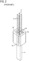
- Fig. 2 illustrates an assembly in a portion A in Fig. 1 .
- the oxygen sensor includes a ceramic element 11, and the ceramic element 11 is fixed in a main metal shell 12 by, for example, a glass seal 13.
- a cover 15 which covers a projecting portion of the ceramic element 11 is attached to an outer perimeter of a distal end of the main metal shell 12. Openings 15a which guide exhaust gas flowing through an exhaust pipe into the cover 15 are formed in the cover 15.
- the ceramic element 11 has an elongated shape and is square in sectional shape.
- Two electrode terminal portions 16 are formed on each of one outer surface and the other outer surface of one end portion of the ceramic element 11 (see Fig. 2 ).
- a conducting wire (specifically an elongated thin metal plate) 17 is connected to each electrode terminal portion 16.
- Each conducting wire 17 is connected to a lead wire 19 via a connector portion 18.
- Four lead wires 19 extend through a grommet 21 and extend further to outside the grommet 21. Distal end portions of the four lead wires 19 are coupled to a connector plug 22.
- Reference numeral 14 in Fig. 1 denotes a cylindrical metal casing
- reference numeral 23 denotes a protective tube which protects the lead wires 19.
- a coupling unit 25 which is composed of the ceramic element 11, the conducting wires 17, and insulating plates 24 is constructed by placing one conducting wire 17 on each electrode terminal portion 16 and placing the insulating plates 24 on the conducting wires 17.
- the electrode terminal portions 16 and the conducting wires 17 are connected to each other by tightening the coupling unit 25 with a metal ring 26 such that the coupling unit 25 fits tightly, as illustrated in Fig. 2 .
- the coupling unit 25 is tightened up by the metal ring 26, and each conducting wire 17 is pressed onto the electrode terminal portion 16 of the ceramic element 11.
- the electrode terminal portion 16 and the conducting wire 17 are electrically connected to each other.
- connection forces differ due to variation in dimensions among the ceramic elements 11 or the insulating plates 24 that are components of the coupling units 25, and a stable contact force may not be obtained between the conducting wire 17 and the electrode terminal portion 16.
- the coupling unit 25 is composed of high-rigidity members, a large force is needed in the process of press-fitting into the metal ring 26, and assembly work is difficult.
- An object of this invention is to provide a connector capable of being electrically connected to a ceramic element of a ceramic applied electronic device with good reliability and workability and a ceramic applied electronic device including the connector.
- a connector according to the present invention includes two insulators, two spring components, and a cylindrical sleeve.
- the two spring components are mounted on the two insulators for holding a ceramic element from two sides.
- a spring portion of each of the two spring components has an inclined surface which inclines in a movement direction in which the cylindrical sleeve moves toward the two spring components.
- the spring portion is elastically deformed when the cylindrical sleeve hangs over the spring portion.
- the two elastically deformed spring components push the two insulators so as to bring the two insulators closer to each other, and the two insulators tightly hold the ceramic element from the two sides. In this state, contacts mounted on each of the two insulators are pushed hard against terminal electrodes of the ceramic element.
- a ceramic applied electronic device according to the present invention includes the above-described connector.
- a connector according to this invention can be electrically connected to a ceramic element of a ceramic applied electronic device with good reliability and workability.
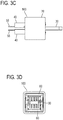
- FIGs. 3A, 3B , 3C, 3D , 4A, and 4B illustrate a configuration of a connector according to a first embodiment.
- a connector 100 is used to connect a ceramic element incorporated in a ceramic applied electronic device and lead wires for connection with an external apparatus.
- Figs. 3A, 3B , 3C, 3D , 4A, and 4B illustrate the connector 100, to which a ceramic element 30 is connected.
- the connector 100 includes two insulators 40, eight contacts 50, two spring components 60, and a cylindrical sleeve 70 which is hollow and rectangular in sectional shape.
- Fig. 5 is a partial exploded view of the connector 100, and Figs. 6A and 6B illustrate details of the insulator 40.
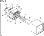
- Figs. 7A , 7B , and 8 illustrate the connector 100, to which the ceramic element 30 is not connected.
- the two insulators 40 each hold four contacts 50 aligned at a lower surface 40a.
- the two insulators 40 are arranged such that the lower surface 40a of one of the two insulators 40 and the lower surface 40a of the other face each other.
- Four grooves 41, four holes 42 and stopping portions 43 are formed at the insulator 40, as illustrated in Figs. 6A and 6B , the four grooves 41 housing distal ends of the contacts 50 which catch on the four grooves 41, the four holes 42 receiving insertion of parts of the contacts 50, and the stopping portions 43 stopping the contacts 50.
- Each stopping portion 43 is located in the hole 42.
- a projecting portion 44 is formed at one end in a width direction (that is, an array direction of the grooves 41) of the lower surface 40a of the insulator 40, and regulation portions 45 and 46 project at the other end.
- the projecting portion 44 and the regulation portions 45 and 46 serve as spacers.
- the projecting portion 44 of the one insulator 40 is located between the regulation portions 45 and 46 of the other insulator 40, and the projecting portion 44 of the other insulator 40 is located between the regulation portions 45 and 46 of the one insulator 40.
- a recessed portions 47 is formed at each of two corners in the width direction of one end having the grooves 41.
- Two projections 48 are formed at an upper surface 40b of the insulator 40, and positions of the two projections 48 substantially correspond to positions of the recessed portions 47 of the lower surface 40a.
- the insulator 40 is made of ceramic, such as an alumina sintered body.
- the contact 50 is held by the insulator 40, as illustrated in Figs. 5 , 7A , and 7B .
- the contact 50 includes a distal end portion 51 in a curved shape, contact portions 52 and 53 which are slightly bent, a rising portion 54 which is to be inserted into the hole 42 of the insulator 40, a hook portion 55 which is formed at a distal end of the rising portion 54, and a connection portion 56 which extends straight.
- the distal end portion 51 is housed in the groove 41 of the insulator 40 by being hooked around the groove 41 of the insulator 40.
- the contact portions 52 and 53 are electric contacts which are to come into contact with a terminal electrode of the ceramic element 30.
- the hook portion 55 is hooked on the stopping portion 43 of the insulator 40.
- the connection portion 56 is led out from the insulator 40.
- the spring component 60 made of metal is a plate portion which is turned back by approximately 180 degrees, as illustrated in Figs. 5 , 7A , and 7B , and has a square flat plate portion 61, a turnback piece 62 which is continuous with one end of the flat plate portion 61 and extends from the one end of the flat plate portion 61 toward the other end of the flat plate portion 61, and two hook portions 63 which project from two end portions in the width direction of a distal end of the turnback piece 62.
- the hook portions 63 are bent in a staple shape.
- the turnback piece 62 functions as a spring portion (spring piece), and a bent portion 62a is formed in the middle in an extension direction of the turnback piece 62.
- the turnback piece 62 has a V-shape in which the bent portion 62a is farther from the flat plate portion 61.
- An inclined surface 62b which gradually becomes farther from the flat plate portion 61 in a direction from the hook portions 63 toward the bent portion 62a is formed between the bent portion 62a and the hook portions 63.
- the spring component 60 is formed of, for example, a stainless material, and the cylindrical sleeve 70 is also formed of a stainless material.
- the spring component 60 is mounted on each of the two insulators 40 holding the contacts 50.
- each flat plate portion 61 is located on the upper surface 40b of the insulator 40, and distal ends of the two hook portions 63 are located in the recessed portions 47 of the lower surface 40a of the insulator 40 to hook the two hook portions 63 on the insulator 40.
- the flat plate portion 61 butts against the two projections 48, which prevents the spring component 60 from coming off from the insulator 40.
- the two insulators 40 with the spring components 60 mounted on the upper surfaces 40b, that is, outer surfaces are arranged such that the lower surfaces 40a face each other, as illustrated in Figs. 7A , 7B , and 8 .
- the two insulators 40 are positioned by a jig (not illustrated), and a spacing between the contact portions 52 (53) of the contacts 50 facing each other is indicated by d1 (see Fig. 7B ).
- Four terminal electrodes 32 are arrayed on a surface on the obverse side of the base end portion 31, as illustrated in Figs. 7A and 8 , and four terminal electrodes 32 are also arrayed on a surface on the reverse side.
- the terminal electrodes 32 are not illustrated in detail in Figs. 7B , 3B , and 4B .
- the ceramic element 30 Before insertion of the base end portion 31 between the two insulators 40, the ceramic element 30 is passed through the sleeve 70.
- the base end portion 31 of the ceramic element 30 after the passage through the sleeve 70 is inserted between the two insulators 40 (see Fig. 9 ).
- the sleeve 70 is moved, that is, slid to a position illustrated in Figs. 3A and 4B , thereby completing connection of the connector 100 and the ceramic element 30.
- the positioning jig described above is released from the two insulators 40.
- Letting t be a thickness of the ceramic element 30, as illustrated in Fig. 7B , the spacing d1 between the contact portions 52 of the contacts 50 facing each other and the thickness t satisfy d1 ⁇ t. The same applies to the spacing d1 between the contact portions 53 of the contacts 50 facing each other.
- the ceramic element 30 can be inserted between the two insulators 40 without the need for an insertion force. That is, the ceramic element 30 can be inserted with a zero insertion force (ZIF). d1 may be set slightly smaller than t. In this case, the ceramic element 30 can be inserted with a slight insertion force. That is, the ceramic element 30 can be inserted with a low insertion force (LIF).
- ZIF zero insertion force
- LIF low insertion force
- the inclined surface 62b has a slope descending gently toward the sleeve 70 that travels toward the spring component 60 and does not interfere with movement of the sleeve 70. Additionally, with a force received from the sleeve 70, the inclined surface 62b inclines toward the insulator 40.
- the sleeve 70 hangs over the turnback pieces 62 of the two spring components 60, and elastically deforms the two turnback pieces 62 in a direction in which the bent portions 62a are brought closer to each other by pushing the bent portions 62a.
- the two insulators 40 located on the two surfaces of the base end portion 31 of the ceramic element 30 are pushed by the flat plate portions 61 of the two spring components 60 to tightly hold the base end portion 31 from two sides. That is, the two insulators 40 firmly hold the ceramic element 30.
- the contact portions 52 and 53 of each contact 50 held by the insulator 40 are pushed against the terminal electrode 32 formed on the base end portion 31, which results in mutual electrical connection between the contact 50 and the terminal electrode 32.
- the turnback piece 62 is elastically deformed, the other end of the flat plate portion 61 is pressed by the distal end of the turnback piece 62, as illustrated in Fig. 4B . Accordingly, the whole of the flat plate portion 61 comes into good contact with the upper surface 40b of the insulator 40.
- the flat plate portion 61 is thus capable of pushing the insulator 40 in a balanced manner.
- the turnback piece 62 is made to function as a spring, which increases a contact force between the spring component 60 and the insulator 40.
- the turnback pieces 62 of the two spring components 60 are structured to hold the two insulators 40 and the base end portion 31 of the ceramic element 30 from two sides when elastically deformed.
- the structure accommodates the variation in dimensions, and a stable contact force is obtained. That is, the connector 100 is excellent in connection reliability between the connector 100 and the ceramic element 30 and is excellent in connection operability and can be connected to the ceramic element 30 with a small operational force.
- the insulator 40 Since the insulator 40 is pushed by a large surface of the flat plate portion 61 of the spring component 60, the insulator 40 made of ceramic is in no danger of breaking by a local force.
- m1 be a dimension between the upper surfaces 40b of the two insulators 40 in the state shown in Fig. 7B
- m2 be a dimension between the upper surfaces 40b of the two insulators 40 in the state shown in Fig. 4B
- m2 ⁇ m1 holds.
- the lead wires for connection with an external apparatus are connected to the connection portions 56 of the contacts 50 of the connector 100, and the terminal electrodes 32 of the ceramic element 30 and the lead wires are electrically connected to each other by the connector 100.
- a ceramic applied electronic device which includes the above-described connector 100 will next be described.
- Fig. 10 illustrates a gas sensor which is a ceramic applied electronic device according to the embodiment.
- the gas sensor includes the ceramic element 30 that detects a predetermined gas component from gas to be detected, a protective cover 80 which protects a distal end portion of the ceramic element 30, and a sensor assembly 90 which includes the connector 100 connected to the ceramic element 30.
- the ceramic element 30 has an elongated plate-like shape and has, for example, a structure in which six ceramic substrates composed of oxygen-ion-conducting solid electrolyte layers made of yttria-stabilized zirconia are stacked.
- the protective cover 80 includes an inner protective cover 81 which covers a distal end of the ceramic element 30 and an outer protective cover 82 which covers the inner protective cover 81.
- the inner protective cover 81 has a hole 81a for introduction of the gas to be detected at the distal end of the ceramic element 30, and the outer protective cover 82 has holes 82a for introduction of the gas to be detected at a side surface.
- the sensor assembly 90 includes a main metal shell 91, an internal cylinder 92 and an external cylinder 93 which are fixed to the main metal shell 91 through welding, and the connector 100 that is connected to the base end portion 31 of the ceramic element 30.
- reference character 91a denotes a threaded portion for mounting which is formed at the main metal shell 91.
- the external cylinder 93 surrounds the internal cylinder 92, a part of the ceramic element 30, and the connector 100.
- Lead wires 96 which are connected to the contacts 50 of the connector 100 are led out from the sensor assembly 90.
- the lead wires 96 are electrically connected to the terminal electrodes 32 of the ceramic element 30 via the connector 100.
- a gap between the external cylinder 93 and the lead wires 96 is sealed with a rubber plug 97.
- the above-described gas sensor is mounted on, for example, an exhaust gas pipe of a vehicle and is used to detect a gas component (for example, NO x or O 2 ) contained in exhaust gas. Since the connector 100 is used to connect the ceramic element 30 and the lead wires 96, high-reliability electrical connection of the ceramic element 30 and the lead wires 96 is implemented. Additionally, mounting of the connector 100 on the ceramic element 30 is easy (good workability).
- a gas component for example, NO x or O 2
- a configuration of a connector according to a second embodiment for connection of terminal electrodes of a ceramic element and lead wires will be described.
- Figs. 11A and 11B illustrate a connector 200, to which a ceramic element 30 is connected.
- Fig. 12 is a partial exploded view of the connector 200.
- Figs. 13A and 13B illustrate details of an insulator 40'.
- Figs. 14A and 14B illustrate the connector 200, to which the ceramic element 30 is not connected. Same constituent elements as those of the connector 100 are denoted by same reference characters, and a detailed description thereof will be omitted.
- the connector 200 is the same as the connector 100 except for shapes of two spring components 60' and shapes of two insulators 40'.
- the spring component 60' has a square flat plate portion 61, two turnback pieces 64, and two mounting pieces 65, as illustrated in Figs. 12 , 14A, and 14B .
- the two turnback pieces 64 are continuous with two ends of the flat plate portion 61 in a traveling direction of a sleeve 70 which travels toward the spring component 60' and extend toward a center of the flat plate portion 61 like folding wings, and distal ends 64a of the two turnback pieces 64 face each other.
- the two turnback pieces 64 function as spring portions (spring pieces).
- the distal end 64a of the turnback piece 64 is slightly bent inward (that is, toward a side with the flat plate portion 61).
- the two mounting pieces 65 are continuous with two ends of the flat plate portion 61 in a width direction (that is, a direction orthogonal to the traveling direction of the sleeve 70) of the spring component 60' and extend in a normal direction of the flat plate portion 61.
- the two mounting pieces 65 are located on one side of the flat plate portion 61 while the two turnback pieces 64 are located on the opposite side of the flat plate portion 61.
- a window 66 is formed in each of the two mounting pieces 65.
- the insulator 40' does not have the recessed portions 47 and the projections 48, unlike the insulator 40.
- a recessed portion 49 is formed in each of side surfaces 40c and 40d of the insulator 40' which are located at two ends in an array direction of four grooves 41, and a claw portion 49a is formed at the recessed portion 49.
- the insulator 40' is made of ceramic, such as an alumina sintered body.
- the spring component 60' is mounted on the insulator 40' by placing the flat plate portion 61 on an upper surface 40b of the insulator 40' and hooking the windows 66 of the two mounting pieces 65 on the claw portions 49a of the insulator 40'.
- Two insulators 40' with the spring components 60' mounted thereon are arranged such that lower surfaces 40a holding contacts 50 face each other, as illustrated in Figs. 14A and 14B .
- a base end portion 31 of the ceramic element 30 is inserted between the two insulators 40'. Connection of the connector 200 and the ceramic element 30 is completed by positioning the sleeve 70 at the position illustrated in Figs. 11A and 11B after the insertion.
- the sleeve 70 hangs over the turnback pieces 64 of the two spring components 60', and elastically deforms the turnback pieces 64 by pushing the distal ends 64a of the turnback pieces 64.
- the two insulators 40' located on two surfaces of the base end portion 31 of the ceramic element 30 are pushed by the flat plate portions 61 of the two spring components 60' to tightly hold the base end portion 31 from two sides. That is, the two insulators 40' firmly hold the ceramic element 30.
- the contact 50 and a terminal electrode 32 formed on the base end portion 31 are electrically connected to each other.
- each turnback piece 64 has an inclined surface 64b which gradually becomes farther from the flat plate portion 61 in a direction from a base portion (that is, a site near a boundary between the turnback piece 64 and the flat plate portion 61) of the turnback piece 64 toward the distal end of the turnback piece 64.
- the inclined surface 64b has a slope descending gently toward the sleeve 70 that travels toward the spring component 60' and does not interfere with movement of the sleeve 70. Additionally, with a force received from the sleeve 70, the turnback piece 64 inclines toward the insulator 40'.
- a configuration of a connector according to a third embodiment for connection of terminal electrodes of a ceramic element and lead wires will be described.
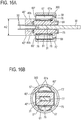
- Figs. 15A, 15B , 15C, 15D , 16A, and 16B illustrate a connector 300 according to the third embodiment, to which a ceramic element 30 is connected.
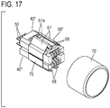
- Fig. 17 is a partial exploded view of the connector 300.
- Figs. 18A and 18B illustrate details of an insulator 40".
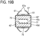
- Figs. 19A and 19B illustrate the connector 300, to which the ceramic element 30 is not connected. Same constituent elements as those of the connector 100 are denoted by same reference characters, and a detailed description thereof will be omitted.
- the spring component 60" has a square flat plate portion 61 and two turnback pieces 67, as illustrated in Figs. 17 , 19A , and 19B .
- the two turnback pieces 67 are continuous with two ends of the flat plate portion 61 in a direction perpendicular to a traveling direction of a sleeve 70' which travels toward the spring component 60" and extend toward a center of the flat plate portion 61 like folding wings, and distal ends 67a of the two turnback pieces 67 face each other.
- the two turnback pieces 67 function as spring portions (spring pieces).
- the distal end 67a of the turnback piece 67 is bent inward and is almost parallel to the flat plate portion 61.
- a projecting portion 68 which projects in the traveling direction of the sleeve 70' that travels toward the spring component 60" is formed at a front end portion (that is, one corner of the distal end 67a) of each of the two turnback pieces 67.
- Each projecting portion 68 has an inclined surface with a slope descending gently toward the sleeve 70' that travels toward the spring component 60".
- a slight notch 69 is formed in a central portion of each of the two ends of the flat plate portion 61 in the traveling direction of the sleeve 70' that travels toward the spring component 60".
- the insulator 40" does not have the recessed portions 47 and the projections 48, unlike the insulator 40.
- a recessed portion 40e which extends from one end to the other end in a width direction (that is, an array direction of four grooves 41) is formed in a middle portion of an upper surface 40b.
- the insulator 40" is also made of ceramic, such as an alumina sintered body.
- the spring component 60" is mounted on the insulator 40" using a metal fitting 75.
- the metal fitting 75 is formed by bending a metal plate and has a section in a hollow square shape.
- the metal fitting 75 is located in the recessed portions 40e of the two insulators 40" and holds the two insulators 40" from two sides.
- Two fixing pieces 76 project from two ends of a portion of the metal fitting 75, which is located in the recessed portion 40e of the insulator 40", in the traveling direction of the sleeve 70' that travels toward the spring component 60".
- a position of the fixing piece 76 corresponds to a position of the notch 69 formed in the flat plate portion 61 of the spring component 60".
- the flat plate portion 61 is fixed by bending the fixing pieces 76 after passage through the notches 69.
- the spring component 60" is mounted on the metal fitting 75.
- the metal fitting 75 and the two spring components 60" are mounted on the two insulators 40" holding contacts 50.
- a base end portion 31 of the ceramic element 30 is inserted between the two insulators 40" in the state illustrated in Figs. 19A and 19B .
- Connection of the connector 300 and the ceramic element 30 is completed by positioning the circular cylindrical sleeve 70' at the position illustrated in Figs. 15A, 15B , 15C, 15D , 16A, and 16B after the insertion.
- the sleeve 70' hangs over the turnback pieces 67 of the two spring components 60", and elastically deforms the turnback pieces 67 by pushing the distal ends 67a of the turnback pieces 67.
- the two insulators 40" located on two surfaces of the base end portion 31 of the ceramic element 30 are pushed by the flat plate portions 61 of the two spring components 60" along with the metal fitting 75 between the two insulators 40" and the flat plate portions 61 to tightly hold the base end portion 31 from two sides. That is, the two insulators 40" firmly hold the ceramic element 30.
- the contact 50 and a terminal electrode 32 formed on the base end portion 31 are electrically connected to each other.
- the projecting portion 68 has a slope descending gently toward the sleeve 70' that travels toward the spring component 60" and does not interfere with movement of the sleeve 70'. Additionally, with a force received from the sleeve 70', the turnback piece 67 inclines toward the insulator 40".
- a large opening 77 is formed in a portion of the metal fitting 75 which faces one of combinations, each having side surfaces 40c and 40d, of the two insulators 40".
- the opening 77 is deformed to cause portions of the metal fitting 75 which are located in the recessed portions 40e of the two insulators 40" to follow the recessed portions 40e well.
- the connectors 200 and 300 according to the second and third embodiments can also be used to connect the ceramic element 30 and the lead wires 96 in a ceramic applied electronic device and can be electrically connected to the ceramic element 30 with good workability and excellent reliability.
- Shapes of the sleeves 70 and 70' are each, for example, a circular cylindrical shape or a cylindrical shape which is hollow and polygonal in sectional shape.
- connection In the claims and the specification, unless otherwise noted, "connect”, “join”, “couple”, “interlock”, or synonyms therefor and all the word forms thereof, if any, do not necessarily deny the presence of one or more intermediate elements between two elements, for instance, two elements “connected” or “joined” to each other or “interlocked” with each other. Connection between elements, if required, may be physical connection, electrical connection, or a combination thereof.
Landscapes
- Chemical & Material Sciences (AREA)
- Life Sciences & Earth Sciences (AREA)
- Health & Medical Sciences (AREA)
- Physics & Mathematics (AREA)
- Chemical Kinetics & Catalysis (AREA)
- Electrochemistry (AREA)
- Molecular Biology (AREA)
- Analytical Chemistry (AREA)
- Biochemistry (AREA)
- General Health & Medical Sciences (AREA)
- General Physics & Mathematics (AREA)
- Immunology (AREA)
- Pathology (AREA)
- Details Of Connecting Devices For Male And Female Coupling (AREA)
- Measuring Oxygen Concentration In Cells (AREA)
Abstract
Description
- This invention relates to a ceramic applied electronic device, such as a nitrogen oxides (NOx) sensor or an oxygen sensor incorporating a ceramic element, and also relates to a connector used in the ceramic applied electronic device.
-
Fig. 1 illustrates an oxygen sensor for detecting the concentration of oxygen in exhaust gas from a vehicle, which is disclosed as a prior art associated with a ceramic applied electronic device in Japanese Patent Application Laid Open No.H10-253579 Fig. 2 illustrates an assembly in a portion A inFig. 1 . - The oxygen sensor includes a
ceramic element 11, and theceramic element 11 is fixed in amain metal shell 12 by, for example, aglass seal 13. Acover 15 which covers a projecting portion of theceramic element 11 is attached to an outer perimeter of a distal end of themain metal shell 12.Openings 15a which guide exhaust gas flowing through an exhaust pipe into thecover 15 are formed in thecover 15. - The
ceramic element 11 has an elongated shape and is square in sectional shape. Twoelectrode terminal portions 16 are formed on each of one outer surface and the other outer surface of one end portion of the ceramic element 11 (seeFig. 2 ). A conducting wire (specifically an elongated thin metal plate) 17 is connected to eachelectrode terminal portion 16. Each conductingwire 17 is connected to alead wire 19 via aconnector portion 18. Fourlead wires 19 extend through agrommet 21 and extend further to outside thegrommet 21. Distal end portions of the fourlead wires 19 are coupled to aconnector plug 22.Reference numeral 14 inFig. 1 denotes a cylindrical metal casing, andreference numeral 23 denotes a protective tube which protects thelead wires 19. - A
coupling unit 25 which is composed of theceramic element 11, the conductingwires 17, andinsulating plates 24 is constructed by placing one conductingwire 17 on eachelectrode terminal portion 16 and placing theinsulating plates 24 on the conductingwires 17. Theelectrode terminal portions 16 and the conductingwires 17 are connected to each other by tightening thecoupling unit 25 with ametal ring 26 such that thecoupling unit 25 fits tightly, as illustrated inFig. 2 . - That is, the
coupling unit 25 is tightened up by themetal ring 26, and each conductingwire 17 is pressed onto theelectrode terminal portion 16 of theceramic element 11. As a result, theelectrode terminal portion 16 and the conductingwire 17 are electrically connected to each other. - With the above-described connection structure, contact forces differ due to variation in dimensions among the
ceramic elements 11 or theinsulating plates 24 that are components of thecoupling units 25, and a stable contact force may not be obtained between the conductingwire 17 and theelectrode terminal portion 16. - Additionally, since the
coupling unit 25 is composed of high-rigidity members, a large force is needed in the process of press-fitting into themetal ring 26, and assembly work is difficult. - An object of this invention is to provide a connector capable of being electrically connected to a ceramic element of a ceramic applied electronic device with good reliability and workability and a ceramic applied electronic device including the connector.
- The following technical matters are described simply to facilitate the understanding of the main points of the present invention, not to limit the invention claimed in the claims explicitly or implicitly and not to express the possibility of accepting such a limitation that is imposed by a person other than those who will benefit from the present invention (for example, the applicant and the right holder). The general outline of the present invention described from other perspectives can be understood from, for example, the claims of this application as originally filed at the time of application.
- A connector according to the present invention includes two insulators, two spring components, and a cylindrical sleeve. The two spring components are mounted on the two insulators for holding a ceramic element from two sides. A spring portion of each of the two spring components has an inclined surface which inclines in a movement direction in which the cylindrical sleeve moves toward the two spring components. The spring portion is elastically deformed when the cylindrical sleeve hangs over the spring portion. The two elastically deformed spring components push the two insulators so as to bring the two insulators closer to each other, and the two insulators tightly hold the ceramic element from the two sides. In this state, contacts mounted on each of the two insulators are pushed hard against terminal electrodes of the ceramic element.
- A ceramic applied electronic device according to the present invention includes the above-described connector.
- These and other objects, features and advantages of the present invention will become apparent from the detailed description taken in conjunction with the accompanying drawings.
- A connector according to this invention can be electrically connected to a ceramic element of a ceramic applied electronic device with good reliability and workability.
- The subject matter, which is regarded as the invention, is particularly pointed out and distinctly claimed in the claims at the conclusion of the specification. The present invention itself, and manner in which it may be made or used, if any, may be better understood after a review of the following description in connection with the accompanying drawings in which:
-
Fig. 1 is a sectional view of a ceramic applied electronic device according to a conventional technique; -
Fig. 2 is a perspective view illustrating details of a portion A inFig. 1 ; -
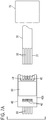
Fig. 3A is a plan view of a connector according to a first embodiment, to which a ceramic element is connected; -
Fig. 3B is a left side view of the connector according to the first embodiment, to which the ceramic element is connected; -
Fig. 3C is a front view of the connector according to the first embodiment, to which the ceramic element is connected; -
Fig. 3D is a right side view of the connector according to the first embodiment, to which the ceramic element is connected; -
Fig. 4A is a perspective view of the connector according to the first embodiment, to which the ceramic element is connected; -
Fig. 4B is an enlarged sectional view of the connector according to the first embodiment, to which the ceramic element is connected; -
Fig. 5 is a perspective view of the connector according to the first embodiment, which is partially exploded; -
Fig. 6A is a perspective view of an insulator illustrated inFig. 5 ; -
Fig. 6B is an upside-down perspective view of the insulator illustrated inFig. 6A ; -
Fig. 7A is a plan view of the connector according to the first embodiment, to which the ceramic element is not connected; -
Fig. 7B is a sectional view of the connector according to the first embodiment, to which the ceramic element is not connected; -
Fig. 8 is a perspective view of the connector according to the first embodiment, to which the ceramic element is not connected; -
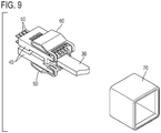
Fig. 9 is a perspective view illustrating the connector according to the first embodiment, to which a sleeve is not attached; -
Fig. 10 is a sectional view illustrating a ceramic applied electronic device according to the embodiment; -
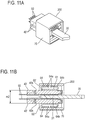
Fig. 11A is a perspective view of a connector according to a second embodiment, to which a ceramic element is connected; -
Fig. 11B is an enlarged sectional view of the connector according to the second embodiment, to which the ceramic element is connected; -
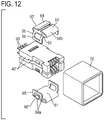
Fig. 12 is a perspective view of the connector according to the second embodiment, which is partially exploded; -
Fig. 13A is a perspective view of an insulator illustrated inFig. 12 ; -
Fig. 13B is an upside-down perspective view of the insulator illustrated inFig. 13A ; -
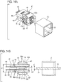
Fig. 14A is a perspective view of the connector according to the second embodiment, to which the ceramic element is not connected; -
Fig. 14B is an enlarged sectional view of the connector according to the second embodiment, to which the ceramic element is not connected; -
Fig. 15A is a plan view of a connector according to a third embodiment, to which a ceramic element is connected; -
Fig. 15B is a front view of the connector according to the third embodiment, to which the ceramic element is connected; -
Fig. 15C is a right side view of the connector according to the third embodiment, to which the ceramic element is connected; -
Fig. 15D is a perspective view of the connector according to the third embodiment, to which the ceramic element is connected; -
Fig. 16A is an enlarged sectional view taken along line E-E inFig. 15A ; -
Fig. 16B is an enlarged sectional view taken along line F-F inFig. 15B ; -
Fig. 17 is a perspective view of the connector according to the third embodiment, which is partially exploded; -
Fig. 18A is a perspective view of an insulator illustrated inFig. 17 ; -
Fig. 18B is an upside-down perspective view of the insulator illustrated inFig. 18A ; -
Fig. 19A is a sectional view of the connector according to the third embodiment, to which the ceramic element is not connected; and -
Fig. 19B is a sectional view taken along line C-C inFig. 19A . - With regard to reference numerals used, the following numbering is used throughout the drawings.
- 11:
- ceramic element
- 12:
- main metal shell
- 13:
- glass seal
- 14:
- cylindrical metal casing
- 15:
- cover
- 15a:
- opening
- 16:
- electrode terminal portion
- 17:
- conducting wire
- 18:
- connector portion
- 19:
- lead wire
- 21:
- grommet
- 22:
- connector plug
- 23:
- protective tube
- 24:
- insulating plate
- 25:
- coupling unit
- 26:
- metal ring
- 30:
- ceramic element
- 31:
- base end portion
- 32:
- terminal electrode
- 40:
- insulator
- 40':
- insulator
- 40":
- insulator
- 40a:
- lower surface
- 40b:
- upper surface
- 40c:
- side surface
- 40d:
- side surface
- 40e:
- recessed portion
- 41:
- groove
- 42:
- hole
- 43:
- stopping portion
- 44:
- projecting portion
- 45:
- regulation portion
- 46:
- regulation portion
- 47:
- recessed portion
- 48:
- projection
- 49:
- recessed portion
- 49a:
- claw portion
- 50:
- contact
- 51:
- distal end portion
- 52:
- contact portion
- 53:
- contact portion
- 54:
- rising portion
- 55:
- hook portion
- 56:
- connection portion
- 60:
- spring component
- 60':
- spring component
- 60":
- spring component
- 61:
- flat plate portion
- 62:
- turnback piece
- 62a:
- bent portion
- 62b:
- inclined surface
- 63:
- hook portion
- 64:
- turnback piece
- 64a:
- distal end
- 64b:
- inclined surface
- 65:
- mounting piece
- 66:
- window
- 67:
- turnback piece
- 67a:
- distal end
- 68:
- projecting portion
- 69:
- notch
- 70:
- sleeve
- 70':
- sleeve
- 75:
- metal fitting
- 76:
- fixing piece
- 77:
- opening
- 80:
- protective cover
- 81:
- inner protective cover
- 81a:
- hole
- 82:
- outer protective cover
- 82a:
- hole
- 90:
- sensor assembly
- 91:
- main metal shell
- 91a:
- threaded portion
- 92:
- internal cylinder
- 93:
- external cylinder
- 94a:
- ceramic supporter
- 94b:
- ceramic supporter
- 94c:
- ceramic supporter
- 95a:
- ceramic powder
- 95b:
- ceramic powder
- 96:
- lead wire
- 97:
- rubber plug
- 100:
- connector
- 200:
- connector
- 300:
- connector
- Embodiments of this invention will be described with reference to the drawings.
-
Figs. 3A, 3B ,3C, 3D ,4A, and 4B illustrate a configuration of a connector according to a first embodiment. Aconnector 100 is used to connect a ceramic element incorporated in a ceramic applied electronic device and lead wires for connection with an external apparatus.Figs. 3A, 3B ,3C, 3D ,4A, and 4B illustrate theconnector 100, to which aceramic element 30 is connected. - The
connector 100 includes twoinsulators 40, eightcontacts 50, twospring components 60, and acylindrical sleeve 70 which is hollow and rectangular in sectional shape.Fig. 5 is a partial exploded view of theconnector 100, andFigs. 6A and 6B illustrate details of theinsulator 40.Figs. 7A ,7B , and8 illustrate theconnector 100, to which theceramic element 30 is not connected. - The two
insulators 40 each hold fourcontacts 50 aligned at alower surface 40a. The twoinsulators 40 are arranged such that thelower surface 40a of one of the twoinsulators 40 and thelower surface 40a of the other face each other. Fourgrooves 41, fourholes 42 and stopping portions 43 (seeFig. 7B ) are formed at theinsulator 40, as illustrated inFigs. 6A and 6B , the fourgrooves 41 housing distal ends of thecontacts 50 which catch on the fourgrooves 41, the fourholes 42 receiving insertion of parts of thecontacts 50, and the stoppingportions 43 stopping thecontacts 50. Each stoppingportion 43 is located in thehole 42. - A projecting
portion 44 is formed at one end in a width direction (that is, an array direction of the grooves 41) of thelower surface 40a of theinsulator 40, andregulation portions portion 44 and theregulation portions insulators 40 are arranged with the onelower surface 40a and the otherlower surface 40a facing each other, the projectingportion 44 of the oneinsulator 40 is located between theregulation portions other insulator 40, and the projectingportion 44 of theother insulator 40 is located between theregulation portions insulator 40. - At the
lower surface 40a of theinsulator 40, a recessedportions 47 is formed at each of two corners in the width direction of one end having thegrooves 41. Twoprojections 48 are formed at anupper surface 40b of theinsulator 40, and positions of the twoprojections 48 substantially correspond to positions of the recessedportions 47 of thelower surface 40a. - The
insulator 40 is made of ceramic, such as an alumina sintered body. - Each
contact 50 is held by theinsulator 40, as illustrated inFigs. 5 ,7A , and7B . Thecontact 50 includes adistal end portion 51 in a curved shape,contact portions portion 54 which is to be inserted into thehole 42 of theinsulator 40, ahook portion 55 which is formed at a distal end of the risingportion 54, and aconnection portion 56 which extends straight. Thedistal end portion 51 is housed in thegroove 41 of theinsulator 40 by being hooked around thegroove 41 of theinsulator 40. Thecontact portions ceramic element 30. Thehook portion 55 is hooked on the stoppingportion 43 of theinsulator 40. Theconnection portion 56 is led out from theinsulator 40. - The
spring component 60 made of metal is a plate portion which is turned back by approximately 180 degrees, as illustrated inFigs. 5 ,7A , and7B , and has a squareflat plate portion 61, aturnback piece 62 which is continuous with one end of theflat plate portion 61 and extends from the one end of theflat plate portion 61 toward the other end of theflat plate portion 61, and twohook portions 63 which project from two end portions in the width direction of a distal end of theturnback piece 62. Thehook portions 63 are bent in a staple shape. - The
turnback piece 62 functions as a spring portion (spring piece), and abent portion 62a is formed in the middle in an extension direction of theturnback piece 62. Theturnback piece 62 has a V-shape in which thebent portion 62a is farther from theflat plate portion 61. Aninclined surface 62b which gradually becomes farther from theflat plate portion 61 in a direction from thehook portions 63 toward thebent portion 62a is formed between thebent portion 62a and thehook portions 63. - The
spring component 60 is formed of, for example, a stainless material, and thecylindrical sleeve 70 is also formed of a stainless material. - The
spring component 60 is mounted on each of the twoinsulators 40 holding thecontacts 50. In a state in which thespring components 60 are mounted on the twoinsulators 40, eachflat plate portion 61 is located on theupper surface 40b of theinsulator 40, and distal ends of the twohook portions 63 are located in the recessedportions 47 of thelower surface 40a of theinsulator 40 to hook the twohook portions 63 on theinsulator 40. Theflat plate portion 61 butts against the twoprojections 48, which prevents thespring component 60 from coming off from theinsulator 40. - The two
insulators 40 with thespring components 60 mounted on theupper surfaces 40b, that is, outer surfaces are arranged such that thelower surfaces 40a face each other, as illustrated inFigs. 7A ,7B , and8 . The twoinsulators 40 are positioned by a jig (not illustrated), and a spacing between the contact portions 52 (53) of thecontacts 50 facing each other is indicated by d1 (seeFig. 7B ). - A
base end portion 31 of theceramic element 30, which is to be connected to lead wires for connection with an external apparatus by theconnector 100, is inserted between the twoinsulators 40 in the state illustrated inFigs. 7A ,7B , and8 . Fourterminal electrodes 32 are arrayed on a surface on the obverse side of thebase end portion 31, as illustrated inFigs. 7A and8 , and fourterminal electrodes 32 are also arrayed on a surface on the reverse side. Theterminal electrodes 32 are not illustrated in detail inFigs. 7B ,3B , and4B . - Before insertion of the
base end portion 31 between the twoinsulators 40, theceramic element 30 is passed through thesleeve 70. Thebase end portion 31 of theceramic element 30 after the passage through thesleeve 70 is inserted between the two insulators 40 (seeFig. 9 ). After the insertion, thesleeve 70 is moved, that is, slid to a position illustrated inFigs. 3A and4B , thereby completing connection of theconnector 100 and theceramic element 30. When thesleeve 70 is positioned at the position illustrated inFigs. 3A and4B , the positioning jig described above is released from the twoinsulators 40. - Letting t be a thickness of the
ceramic element 30, as illustrated inFig. 7B , the spacing d1 between thecontact portions 52 of thecontacts 50 facing each other and the thickness t satisfy d1 ≥ t. The same applies to the spacing d1 between thecontact portions 53 of thecontacts 50 facing each other. - Thus, the
ceramic element 30 can be inserted between the twoinsulators 40 without the need for an insertion force. That is, theceramic element 30 can be inserted with a zero insertion force (ZIF). d1 may be set slightly smaller than t. In this case, theceramic element 30 can be inserted with a slight insertion force. That is, theceramic element 30 can be inserted with a low insertion force (LIF). - The
inclined surface 62b has a slope descending gently toward thesleeve 70 that travels toward thespring component 60 and does not interfere with movement of thesleeve 70. Additionally, with a force received from thesleeve 70, theinclined surface 62b inclines toward theinsulator 40. - In a state in which connection of the
connector 100 and theceramic element 30 is completed, thesleeve 70 hangs over theturnback pieces 62 of the twospring components 60, and elastically deforms the twoturnback pieces 62 in a direction in which thebent portions 62a are brought closer to each other by pushing thebent portions 62a. As a result, the twoinsulators 40 located on the two surfaces of thebase end portion 31 of theceramic element 30 are pushed by theflat plate portions 61 of the twospring components 60 to tightly hold thebase end portion 31 from two sides. That is, the twoinsulators 40 firmly hold theceramic element 30. Additionally, thecontact portions contact 50 held by theinsulator 40 are pushed against theterminal electrode 32 formed on thebase end portion 31, which results in mutual electrical connection between thecontact 50 and theterminal electrode 32. - As for the
flat plate portion 61 of thespring component 60 parallel to theupper surface 40b of theinsulator 40, when theturnback piece 62 is elastically deformed, the other end of theflat plate portion 61 is pressed by the distal end of theturnback piece 62, as illustrated inFig. 4B . Accordingly, the whole of theflat plate portion 61 comes into good contact with theupper surface 40b of theinsulator 40. Theflat plate portion 61 is thus capable of pushing theinsulator 40 in a balanced manner. As described above, theturnback piece 62 is made to function as a spring, which increases a contact force between thespring component 60 and theinsulator 40. - As has been described above, the
turnback pieces 62 of the twospring components 60 are structured to hold the twoinsulators 40 and thebase end portion 31 of theceramic element 30 from two sides when elastically deformed. Thus, even if there is variation in dimensions among theinsulators 40 or theceramic elements 30, the structure accommodates the variation in dimensions, and a stable contact force is obtained. That is, theconnector 100 is excellent in connection reliability between theconnector 100 and theceramic element 30 and is excellent in connection operability and can be connected to theceramic element 30 with a small operational force. - Since the
insulator 40 is pushed by a large surface of theflat plate portion 61 of thespring component 60, theinsulator 40 made of ceramic is in no danger of breaking by a local force. - Letting m1 be a dimension between the
upper surfaces 40b of the twoinsulators 40 in the state shown inFig. 7B , and m2 be a dimension between theupper surfaces 40b of the twoinsulators 40 in the state shown inFig. 4B , m2 < m1 holds. - The lead wires for connection with an external apparatus are connected to the
connection portions 56 of thecontacts 50 of theconnector 100, and theterminal electrodes 32 of theceramic element 30 and the lead wires are electrically connected to each other by theconnector 100. - A ceramic applied electronic device which includes the above-described
connector 100 will next be described. -
Fig. 10 illustrates a gas sensor which is a ceramic applied electronic device according to the embodiment. The gas sensor includes theceramic element 30 that detects a predetermined gas component from gas to be detected, aprotective cover 80 which protects a distal end portion of theceramic element 30, and asensor assembly 90 which includes theconnector 100 connected to theceramic element 30. - The
ceramic element 30 has an elongated plate-like shape and has, for example, a structure in which six ceramic substrates composed of oxygen-ion-conducting solid electrolyte layers made of yttria-stabilized zirconia are stacked. - The
protective cover 80 includes an innerprotective cover 81 which covers a distal end of theceramic element 30 and an outerprotective cover 82 which covers the innerprotective cover 81. The innerprotective cover 81 has ahole 81a for introduction of the gas to be detected at the distal end of theceramic element 30, and the outerprotective cover 82 hasholes 82a for introduction of the gas to be detected at a side surface. - The
sensor assembly 90 includes amain metal shell 91, aninternal cylinder 92 and anexternal cylinder 93 which are fixed to themain metal shell 91 through welding, and theconnector 100 that is connected to thebase end portion 31 of theceramic element 30. Referring toFig. 10 , although not illustrated in detail,reference character 91a denotes a threaded portion for mounting which is formed at themain metal shell 91. -
Ceramic supporters 94a to 94c andceramic powders ceramic supporters ceramic supporters internal cylinder 92. Theexternal cylinder 93 surrounds theinternal cylinder 92, a part of theceramic element 30, and theconnector 100. Leadwires 96 which are connected to thecontacts 50 of theconnector 100 are led out from thesensor assembly 90. Thelead wires 96 are electrically connected to theterminal electrodes 32 of theceramic element 30 via theconnector 100. A gap between theexternal cylinder 93 and thelead wires 96 is sealed with arubber plug 97. - The above-described gas sensor is mounted on, for example, an exhaust gas pipe of a vehicle and is used to detect a gas component (for example, NOx or O2) contained in exhaust gas. Since the
connector 100 is used to connect theceramic element 30 and thelead wires 96, high-reliability electrical connection of theceramic element 30 and thelead wires 96 is implemented. Additionally, mounting of theconnector 100 on theceramic element 30 is easy (good workability). - A configuration of a connector according to a second embodiment for connection of terminal electrodes of a ceramic element and lead wires will be described.
-
Figs. 11A and 11B illustrate aconnector 200, to which aceramic element 30 is connected.Fig. 12 is a partial exploded view of theconnector 200.Figs. 13A and 13B illustrate details of an insulator 40'.Figs. 14A and 14B illustrate theconnector 200, to which theceramic element 30 is not connected. Same constituent elements as those of theconnector 100 are denoted by same reference characters, and a detailed description thereof will be omitted. - The
connector 200 is the same as theconnector 100 except for shapes of two spring components 60' and shapes of two insulators 40'. - The spring component 60' has a square
flat plate portion 61, twoturnback pieces 64, and two mountingpieces 65, as illustrated inFigs. 12 ,14A, and 14B . The twoturnback pieces 64 are continuous with two ends of theflat plate portion 61 in a traveling direction of asleeve 70 which travels toward the spring component 60' and extend toward a center of theflat plate portion 61 like folding wings, anddistal ends 64a of the twoturnback pieces 64 face each other. The twoturnback pieces 64 function as spring portions (spring pieces). Thedistal end 64a of theturnback piece 64 is slightly bent inward (that is, toward a side with the flat plate portion 61). - The two mounting
pieces 65 are continuous with two ends of theflat plate portion 61 in a width direction (that is, a direction orthogonal to the traveling direction of the sleeve 70) of the spring component 60' and extend in a normal direction of theflat plate portion 61. The two mountingpieces 65 are located on one side of theflat plate portion 61 while the twoturnback pieces 64 are located on the opposite side of theflat plate portion 61. Awindow 66 is formed in each of the two mountingpieces 65. - The insulator 40' does not have the recessed
portions 47 and theprojections 48, unlike theinsulator 40. A recessedportion 49 is formed in each of side surfaces 40c and 40d of the insulator 40' which are located at two ends in an array direction of fourgrooves 41, and aclaw portion 49a is formed at the recessedportion 49. The insulator 40' is made of ceramic, such as an alumina sintered body. - As illustrated in
Figs. 14A and 14B , the spring component 60' is mounted on the insulator 40' by placing theflat plate portion 61 on anupper surface 40b of the insulator 40' and hooking thewindows 66 of the two mountingpieces 65 on theclaw portions 49a of the insulator 40'. - Two insulators 40' with the spring components 60' mounted thereon are arranged such that
lower surfaces 40a holding contacts 50 face each other, as illustrated inFigs. 14A and 14B . Abase end portion 31 of theceramic element 30 is inserted between the two insulators 40'. Connection of theconnector 200 and theceramic element 30 is completed by positioning thesleeve 70 at the position illustrated inFigs. 11A and 11B after the insertion. - In a state in which connection of the
connector 200 and theceramic element 30 is completed, thesleeve 70 hangs over theturnback pieces 64 of the two spring components 60', and elastically deforms theturnback pieces 64 by pushing the distal ends 64a of theturnback pieces 64. As a result, the two insulators 40' located on two surfaces of thebase end portion 31 of theceramic element 30 are pushed by theflat plate portions 61 of the two spring components 60' to tightly hold thebase end portion 31 from two sides. That is, the two insulators 40' firmly hold theceramic element 30. Thus, thecontact 50 and aterminal electrode 32 formed on thebase end portion 31 are electrically connected to each other. - According to the second embodiment, the insulator 40' can be pushed by a large surface of the
flat plate portion 61 of the spring component 60', as in the first embodiment. Additionally, eachturnback piece 64 has aninclined surface 64b which gradually becomes farther from theflat plate portion 61 in a direction from a base portion (that is, a site near a boundary between theturnback piece 64 and the flat plate portion 61) of theturnback piece 64 toward the distal end of theturnback piece 64. Theinclined surface 64b has a slope descending gently toward thesleeve 70 that travels toward the spring component 60' and does not interfere with movement of thesleeve 70. Additionally, with a force received from thesleeve 70, theturnback piece 64 inclines toward the insulator 40'. - A configuration of a connector according to a third embodiment for connection of terminal electrodes of a ceramic element and lead wires will be described.
-
Figs. 15A, 15B ,15C, 15D ,16A, and 16B illustrate aconnector 300 according to the third embodiment, to which aceramic element 30 is connected.Fig. 17 is a partial exploded view of theconnector 300.Figs. 18A and 18B illustrate details of aninsulator 40".Figs. 19A and19B illustrate theconnector 300, to which theceramic element 30 is not connected. Same constituent elements as those of theconnector 100 are denoted by same reference characters, and a detailed description thereof will be omitted. - The
spring component 60" has a squareflat plate portion 61 and twoturnback pieces 67, as illustrated inFigs. 17 ,19A , and19B . The twoturnback pieces 67 are continuous with two ends of theflat plate portion 61 in a direction perpendicular to a traveling direction of a sleeve 70' which travels toward thespring component 60" and extend toward a center of theflat plate portion 61 like folding wings, anddistal ends 67a of the twoturnback pieces 67 face each other. The twoturnback pieces 67 function as spring portions (spring pieces). Thedistal end 67a of theturnback piece 67 is bent inward and is almost parallel to theflat plate portion 61. - A projecting
portion 68 which projects in the traveling direction of the sleeve 70' that travels toward thespring component 60" is formed at a front end portion (that is, one corner of thedistal end 67a) of each of the twoturnback pieces 67. Each projectingportion 68 has an inclined surface with a slope descending gently toward the sleeve 70' that travels toward thespring component 60". A slight notch 69 (seeFig. 19A ) is formed in a central portion of each of the two ends of theflat plate portion 61 in the traveling direction of the sleeve 70' that travels toward thespring component 60". - The
insulator 40" does not have the recessedportions 47 and theprojections 48, unlike theinsulator 40. A recessedportion 40e which extends from one end to the other end in a width direction (that is, an array direction of four grooves 41) is formed in a middle portion of anupper surface 40b. Theinsulator 40" is also made of ceramic, such as an alumina sintered body. - The
spring component 60" is mounted on theinsulator 40" using ametal fitting 75. Themetal fitting 75 is formed by bending a metal plate and has a section in a hollow square shape. Themetal fitting 75 is located in the recessedportions 40e of the twoinsulators 40" and holds the twoinsulators 40" from two sides. - Two fixing
pieces 76 project from two ends of a portion of themetal fitting 75, which is located in the recessedportion 40e of theinsulator 40", in the traveling direction of the sleeve 70' that travels toward thespring component 60". A position of the fixingpiece 76 corresponds to a position of thenotch 69 formed in theflat plate portion 61 of thespring component 60". As illustrated inFig. 16A , theflat plate portion 61 is fixed by bending the fixingpieces 76 after passage through thenotches 69. As a result, thespring component 60" is mounted on themetal fitting 75. - The
metal fitting 75 and the twospring components 60" are mounted on the twoinsulators 40" holdingcontacts 50. Abase end portion 31 of theceramic element 30 is inserted between the twoinsulators 40" in the state illustrated inFigs. 19A and19B . Connection of theconnector 300 and theceramic element 30 is completed by positioning the circular cylindrical sleeve 70' at the position illustrated inFigs. 15A, 15B ,15C, 15D ,16A, and 16B after the insertion. - In a state in which connection of the
connector 300 and theceramic element 30 is completed, the sleeve 70' hangs over theturnback pieces 67 of the twospring components 60", and elastically deforms theturnback pieces 67 by pushing the distal ends 67a of theturnback pieces 67. As a result, the twoinsulators 40" located on two surfaces of thebase end portion 31 of theceramic element 30 are pushed by theflat plate portions 61 of the twospring components 60" along with the metal fitting 75 between the twoinsulators 40" and theflat plate portions 61 to tightly hold thebase end portion 31 from two sides. That is, the twoinsulators 40" firmly hold theceramic element 30. Thus, thecontact 50 and aterminal electrode 32 formed on thebase end portion 31 are electrically connected to each other. - According to the third embodiment, the projecting
portion 68 has a slope descending gently toward the sleeve 70' that travels toward thespring component 60" and does not interfere with movement of the sleeve 70'. Additionally, with a force received from the sleeve 70', theturnback piece 67 inclines toward theinsulator 40". - A
large opening 77 is formed in a portion of the metal fitting 75 which faces one of combinations, each havingside surfaces insulators 40". Thus, when themetal fitting 75 is pushed by thespring components 60", theopening 77 is deformed to cause portions of the metal fitting 75 which are located in the recessedportions 40e of the twoinsulators 40" to follow the recessedportions 40e well. - The
connectors ceramic element 30 and thelead wires 96 in a ceramic applied electronic device and can be electrically connected to theceramic element 30 with good workability and excellent reliability. - Shapes of the
sleeves 70 and 70' are each, for example, a circular cylindrical shape or a cylindrical shape which is hollow and polygonal in sectional shape. - While the invention has been described with reference to exemplary embodiments, it will be understood by those skilled in the art that various changes may be made and equivalents may be substituted for elements thereof without departing from the scope of the invention. In addition, many modifications may be made to adapt a particular system, device or component thereof to the teachings of the invention without departing from the essential scope thereof. Therefore, it is intended that the invention not be limited to the particular embodiments disclosed for carrying out this invention, but that the invention will include all embodiments falling within the scope of the appended claims.
- Moreover, the use of the terms "first", "second", "i-th", etc., if any, do not denote any order or importance, but rather the terms "first", "second", "i-th", etc. are used to distinguish one element from another. The term "first" does not necessarily mean "coming before all others in order". The terminology used herein is for the purpose of describing particular embodiments only and is not intended to limit the invention in any way. As used herein, the singular forms "a", "an" and "the" are intended to include the plural forms as well, unless the context clearly indicates otherwise. It will be further understood that the terms "comprise", "comprises", and/or "comprising," when used in this specification and/or the appended claims, specify the presence of stated features, steps, operations, elements, and/or components, but do not preclude the presence or addition of one or more other features, steps, operations, elements, components, and/or groups thereof. The same goes for "include", "includes", and/or "including". The term "and/or", if any, includes any and all combinations of one or more of the associated listed items. In the claims and the specification, unless otherwise noted, "connect", "join", "couple", "interlock", or synonyms therefor and all the word forms thereof, if any, do not necessarily deny the presence of one or more intermediate elements between two elements, for instance, two elements "connected" or "joined" to each other or "interlocked" with each other. Connection between elements, if required, may be physical connection, electrical connection, or a combination thereof.
- Unless otherwise defined, all terms (including technical and scientific terms) used herein have the same meaning as commonly understood by those skilled in the art to which the invention belongs. It will be further understood that terms, such as those defined in commonly used dictionaries, should be interpreted as having a meaning that is consistent with their meaning in the context of the relevant art and the present disclosure and will not be interpreted in an idealized or overly formal sense unless expressly so defined herein.
- In describing the invention, it will be understood that a number of techniques and steps are disclosed. Each of these has individual benefit and each can also be used in conjunction with one or more, or in some cases all, of the other disclosed techniques. Accordingly, for the sake of clarity, this description will refrain from repeating every possible combination of the individual techniques or steps in an unnecessary fashion. Nevertheless, the specification and claims should be read with the understanding that such combinations are entirely within the scope of the invention and the claims.
- The corresponding structures, materials, acts, and equivalents of all means or step plus function elements in the claims below, if any, are intended to include any structure, material, or act for performing the function in combination with other claimed elements as specifically claimed.
- The foregoing description of the embodiments of the invention has been presented for the purpose of illustration and description. It is not intended to be exhaustive and to limit the invention to the precise form disclosed. Modifications or variations are possible in light of the above teaching. The embodiments were chosen and described to provide the best illustration of the principles of the invention and its practical application, and to enable one of ordinary skill in the art to utilize the invention in various embodiments and with various modifications as are suited to the particular use contemplated. All such modifications and variations are within the scope of the invention as determined by the appended claims when interpreted in accordance with the breadth to which they are fairly, legally, and equitably entitled.
Claims (10)
- A ceramic applied electronic device which incorporates a ceramic element having terminal electrodes at a base end portion thereof and from which lead wires for connection with an external apparatus are led out, the ceramic applied electronic device comprising:two insulators which hold contacts connected to the lead wires and are arranged on two surfaces of the base end portion;two spring components which are located on respective outer surfaces of the two insulators and each have a flat plate portion parallel to the outer surface and a spring portion supported by the flat plate portion; anda cylindrical sleeve, whereinthe spring portion of each of the two spring components has an inclined surface which inclines in a movement direction in which the sleeve moves toward the two spring components,the spring portion of each of the two spring components is elastically deformed by the sleeve hanging over the spring portion,the two insulators hold the base end portion from two sides by being pushed by the flat plate portions of the two spring components in directions in which the two insulators are brought closer to each other, andthe contacts are pushed against the terminal electrodes.
- The ceramic applied electronic device according to Claim 1, wherein
the spring portion comprises a turnback piece which is continuous with one end of the flat plate portion and extends from the one end of the flat plate portion to the other end of the flat plate portion. - The ceramic applied electronic device according to Claim 2, wherein
the turnback piece has a bent portion,
the turnback piece has a V-shape in which the bent portion is farther from the flat plate portion, and
a distal end of the turnback piece is pushed against the other end of the flat plate portion. - The ceramic applied electronic device according to Claim 1, wherein
the spring portion comprises two turnback pieces which are continuous with two ends of the flat plate portion in the movement direction, and
distal ends of the two turnback pieces face each other. - The ceramic applied electronic device according to Claim 1, wherein
the spring portion comprises two turnback pieces which are continuous with two ends of the flat plate portion in a direction perpendicular to the movement direction,
distal ends of the two turnback pieces face each other, and
a projecting portion which has an inclined surface inclining in the movement direction protrudes from a front end portion of each of the two turnback pieces. - A connector for electrically connecting terminal electrodes on a base end portion of a ceramic element to lead wires, the connector comprising:two insulators which hold contacts connected to the lead wires;two spring components which are located on respective outer surfaces of the two insulators and each have a flat plate portion parallel to the outer surface and a spring portion supported by the flat plate portion; anda cylindrical sleeve, whereinthe spring portion of each of the two spring components has an inclined surface which inclines in a movement direction in which the sleeve moves toward the two spring components,the spring portion of each of the two spring components is elastically deformed in a state in which the sleeve hangs over the spring portion, andthe two insulators hold the base end portion from two sides and push the contacts against the terminal electrodes by being pushed by the flat plate portions of the two spring components in directions in which the two insulators are brought closer to each other when the sleeve hangs over the spring portions.
- The connector according to Claim 6, wherein
the spring portion comprises a turnback piece which is continuous with one end of the flat plate portion and extends from the one end of the flat plate portion to the other end of the flat plate portion. - The connector according to Claim 7, wherein
the turnback piece has a bent portion,
the turnback piece has a V-shape in which the bent portion is farther from the flat plate portion, and
a distal end of the turnback piece comes into contact with the other end of the flat plate portion in a state in which the sleeve hangs over the spring portion. - The connector according to Claim 6, wherein
the spring portion comprises two turnback pieces which are continuous with two ends of the flat plate portion in the movement direction, and
distal ends of the two turnback pieces face each other. - The connector according to Claim 6, wherein
the spring portion comprises two turnback pieces which are continuous with two ends of the flat plate portion in a direction perpendicular to the movement direction,
distal ends of the two turnback pieces face each other, and
a projecting portion which has an inclined surface inclining in the movement direction protrudes from a front end portion of each of the two turnback pieces.
Applications Claiming Priority (1)
| Application Number | Priority Date | Filing Date | Title |
|---|---|---|---|
| JP2019197327A JP7232168B2 (en) | 2019-10-30 | 2019-10-30 | Ceramic applied electronic devices and connectors |
Publications (2)
| Publication Number | Publication Date |
|---|---|
| EP3816619A1 true EP3816619A1 (en) | 2021-05-05 |
| EP3816619B1 EP3816619B1 (en) | 2022-03-23 |
Family
ID=72659053
Family Applications (1)
| Application Number | Title | Priority Date | Filing Date |
|---|---|---|---|
| EP20198203.0A Active EP3816619B1 (en) | 2019-10-30 | 2020-09-24 | Ceramic applied electronic device and connector |
Country Status (4)
| Country | Link |
|---|---|
| US (1) | US11585782B2 (en) |
| EP (1) | EP3816619B1 (en) |
| JP (1) | JP7232168B2 (en) |
| CN (1) | CN112748170A (en) |
Families Citing this family (1)
| Publication number | Priority date | Publication date | Assignee | Title |
|---|---|---|---|---|
| JP7314012B2 (en) | 2019-10-07 | 2023-07-25 | 日本航空電子工業株式会社 | Socket contacts and connectors |
Citations (6)
| Publication number | Priority date | Publication date | Assignee | Title |
|---|---|---|---|---|
| JPH10253579A (en) | 1996-10-14 | 1998-09-25 | Ngk Spark Plug Co Ltd | Ceramic applied electronic device used at high temperature and method of manufacturing the same |
| US7563118B1 (en) * | 2008-06-20 | 2009-07-21 | Delphi Technologies, Inc. | High temperature connector |
| US20090318014A1 (en) * | 2008-06-20 | 2009-12-24 | Delphi Technologies, Inc. | High Temperature Connector Body |
| US20120031171A1 (en) * | 2010-01-19 | 2012-02-09 | Ngk Insulators, Ltd. | Gas sensor and method for making the same |
| US20120192653A1 (en) * | 2009-10-13 | 2012-08-02 | Ngk Insulators, Ltd. | Contact member for gas sensor, gas sensor, constraint member, connecting method of sensor element and contact member of gas sensor, manufacturing method of gas sensor |
| US20120216599A1 (en) * | 2009-11-09 | 2012-08-30 | Ngk Insulators, Ltd. | Gas sensor, contact member of gas sensor and sensor element retaining member for contact member of gas sensor |
Family Cites Families (19)
| Publication number | Priority date | Publication date | Assignee | Title |
|---|---|---|---|---|
| US5246562A (en) * | 1990-10-26 | 1993-09-21 | Robert Bosch Gmbh | Gas measurement sensor, especially for determining oxygen concentration in exhaust gases of internal combustion engines |
| JP2001343356A (en) | 2000-03-30 | 2001-12-14 | Denso Corp | Gas sensor |
| JP4648539B2 (en) | 2000-11-30 | 2011-03-09 | 日本特殊陶業株式会社 | Sensor terminal connection structure |
| JP2004093306A (en) * | 2002-08-30 | 2004-03-25 | Denso Corp | Gas sensor |
| JP2005077122A (en) | 2003-08-28 | 2005-03-24 | Ngk Spark Plug Co Ltd | Sensor and metal terminal |
| JP2008298731A (en) * | 2007-06-04 | 2008-12-11 | Denso Corp | Gas sensor |
| JP4479842B2 (en) * | 2007-10-18 | 2010-06-09 | 株式会社デンソー | Gas sensor and manufacturing method thereof |
| US7798855B2 (en) * | 2007-12-14 | 2010-09-21 | Caterpillar Inc | Connector for sensor assembly |
| JP4961416B2 (en) * | 2008-12-10 | 2012-06-27 | 日本特殊陶業株式会社 | Sensor |
| JP2011133351A (en) | 2009-12-24 | 2011-07-07 | Denso Corp | Gas sensor and method of manufacturing the same |
| EP2554985B1 (en) | 2010-03-31 | 2018-03-21 | NGK Insulators, Ltd. | Contact member for gas sensor and method of connecting sensor elements of gas sensor to contact member |
| JP5582849B2 (en) | 2010-04-02 | 2014-09-03 | 日本航空電子工業株式会社 | Photoelectric composite connection mechanism |
| JP2015145831A (en) | 2014-02-03 | 2015-08-13 | 株式会社デンソー | Gas sensor |
| JP6331891B2 (en) | 2014-08-29 | 2018-05-30 | 株式会社デンソー | Gas sensor |
| JP6593273B2 (en) | 2016-08-01 | 2019-10-23 | 株式会社デンソー | Gas sensor |
| JP6724772B2 (en) * | 2016-12-23 | 2020-07-15 | 株式会社デンソー | Gas sensor |
| JP6981791B2 (en) * | 2017-06-30 | 2021-12-17 | 日本特殊陶業株式会社 | Gas sensor manufacturing method |
| JP7144344B2 (en) | 2019-03-05 | 2022-09-29 | 日本航空電子工業株式会社 | Electric wire connection structure and insulation displacement terminal |
| JP7249262B2 (en) * | 2019-10-30 | 2023-03-30 | 日本航空電子工業株式会社 | Ceramic applied electronic devices and connectors |
-
2019
- 2019-10-30 JP JP2019197327A patent/JP7232168B2/en active Active
-
2020
- 2020-09-02 US US17/010,227 patent/US11585782B2/en active Active
- 2020-09-24 EP EP20198203.0A patent/EP3816619B1/en active Active
- 2020-09-25 CN CN202011022816.6A patent/CN112748170A/en active Pending
Patent Citations (6)
| Publication number | Priority date | Publication date | Assignee | Title |
|---|---|---|---|---|
| JPH10253579A (en) | 1996-10-14 | 1998-09-25 | Ngk Spark Plug Co Ltd | Ceramic applied electronic device used at high temperature and method of manufacturing the same |
| US7563118B1 (en) * | 2008-06-20 | 2009-07-21 | Delphi Technologies, Inc. | High temperature connector |
| US20090318014A1 (en) * | 2008-06-20 | 2009-12-24 | Delphi Technologies, Inc. | High Temperature Connector Body |
| US20120192653A1 (en) * | 2009-10-13 | 2012-08-02 | Ngk Insulators, Ltd. | Contact member for gas sensor, gas sensor, constraint member, connecting method of sensor element and contact member of gas sensor, manufacturing method of gas sensor |
| US20120216599A1 (en) * | 2009-11-09 | 2012-08-30 | Ngk Insulators, Ltd. | Gas sensor, contact member of gas sensor and sensor element retaining member for contact member of gas sensor |
| US20120031171A1 (en) * | 2010-01-19 | 2012-02-09 | Ngk Insulators, Ltd. | Gas sensor and method for making the same |
Also Published As
| Publication number | Publication date |
|---|---|
| JP2021071347A (en) | 2021-05-06 |
| US20210131999A1 (en) | 2021-05-06 |
| JP7232168B2 (en) | 2023-03-02 |
| CN112748170A (en) | 2021-05-04 |
| US11585782B2 (en) | 2023-02-21 |
| EP3816619B1 (en) | 2022-03-23 |
Similar Documents
| Publication | Publication Date | Title |
|---|---|---|
| US11549907B2 (en) | Ceramic applied electronic device and connector | |
| JP4670197B2 (en) | Gas sensor | |
| WO2022177389A1 (en) | Electrically conductive contact pin and assembly thereof | |
| US7568378B2 (en) | Sensor | |
| US8287294B2 (en) | Connector | |
| WO2005090960A1 (en) | Gas sensor | |
| WO2015080332A1 (en) | Shunt resistor and shunt resistor assembly | |
| EP2490016B1 (en) | Contact member for a gas sensor, gas sensor and method for manufacturing a gas sensor | |
| WO2020095679A1 (en) | Probe pin and inspection jig | |
| US20060237315A1 (en) | Gas sensor | |
| EP3816619B1 (en) | Ceramic applied electronic device and connector | |
| US20080295576A1 (en) | Gas sensor having insulator assembly for supporting heater | |
| US7138604B2 (en) | Ceramic device, sensor device, method of making the same, and method for sensing gas | |
| US20040040370A1 (en) | Gas sensor having improved structure of electric connector | |
| CN108701933A (en) | Current measurement in insulator | |
| JP6527042B2 (en) | Wire probe holding structure | |
| JPH0734562U (en) | Conductive connection device | |
| JP2020034352A (en) | Housing for probe pin, inspection jig, inspection unit, and inspection device | |
| JP2002168825A (en) | Sensor terminal connection structure | |
| US20190178828A1 (en) | Gas sensor | |
| US20190162693A1 (en) | Sensor element and gas sensor including the same | |
| US20260086064A1 (en) | Gas sensor | |
| US20250216358A1 (en) | Gas sensor | |
| JPH06258373A (en) | Continuity inspection device for connector housing terminals | |
| JPH03180748A (en) | Gas detecting sensor |
Legal Events
| Date | Code | Title | Description |
|---|---|---|---|
| PUAI | Public reference made under article 153(3) epc to a published international application that has entered the european phase |
Free format text: ORIGINAL CODE: 0009012 |
|
| STAA | Information on the status of an ep patent application or granted ep patent |
Free format text: STATUS: THE APPLICATION HAS BEEN PUBLISHED |
|
| AK | Designated contracting states |
Kind code of ref document: A1 Designated state(s): AL AT BE BG CH CY CZ DE DK EE ES FI FR GB GR HR HU IE IS IT LI LT LU LV MC MK MT NL NO PL PT RO RS SE SI SK SM TR |
|
| RIN1 | Information on inventor provided before grant (corrected) |
Inventor name: HASHIGUCHI, OSAMU |
|
| STAA | Information on the status of an ep patent application or granted ep patent |
Free format text: STATUS: REQUEST FOR EXAMINATION WAS MADE |
|
| 17P | Request for examination filed |
Effective date: 20210720 |
|
| RBV | Designated contracting states (corrected) |
Designated state(s): AL AT BE BG CH CY CZ DE DK EE ES FI FR GB GR HR HU IE IS IT LI LT LU LV MC MK MT NL NO PL PT RO RS SE SI SK SM TR |
|
| GRAP | Despatch of communication of intention to grant a patent |
Free format text: ORIGINAL CODE: EPIDOSNIGR1 |
|
| STAA | Information on the status of an ep patent application or granted ep patent |
Free format text: STATUS: GRANT OF PATENT IS INTENDED |
|
| INTG | Intention to grant announced |
Effective date: 20211115 |
|
| RIN1 | Information on inventor provided before grant (corrected) |
Inventor name: HASHIGUCHI, OSAMU |
|
| GRAS | Grant fee paid |
Free format text: ORIGINAL CODE: EPIDOSNIGR3 |
|
| GRAA | (expected) grant |
Free format text: ORIGINAL CODE: 0009210 |
|
| STAA | Information on the status of an ep patent application or granted ep patent |
Free format text: STATUS: THE PATENT HAS BEEN GRANTED |
|
| AK | Designated contracting states |
Kind code of ref document: B1 Designated state(s): AL AT BE BG CH CY CZ DE DK EE ES FI FR GB GR HR HU IE IS IT LI LT LU LV MC MK MT NL NO PL PT RO RS SE SI SK SM TR |
|
| RAP3 | Party data changed (applicant data changed or rights of an application transferred) |
Owner name: JAPAN AVIATION ELECTRONICS INDUSTRY, LIMITED |
|
| REG | Reference to a national code |
Ref country code: GB Ref legal event code: FG4D |
|
| REG | Reference to a national code |
Ref country code: CH Ref legal event code: EP |
|
| RAP4 | Party data changed (patent owner data changed or rights of a patent transferred) |
Owner name: JAPAN AVIATION ELECTRONICS INDUSTRY, LIMITED |
|
| REG | Reference to a national code |
Ref country code: DE Ref legal event code: R096 Ref document number: 602020002324 Country of ref document: DE |
|
| REG | Reference to a national code |
Ref country code: IE Ref legal event code: FG4D |
|
| REG | Reference to a national code |
Ref country code: AT Ref legal event code: REF Ref document number: 1477779 Country of ref document: AT Kind code of ref document: T Effective date: 20220415 |
|
| REG | Reference to a national code |
Ref country code: LT Ref legal event code: MG9D |
|
| REG | Reference to a national code |
Ref country code: NL Ref legal event code: MP Effective date: 20220323 |
|
| PG25 | Lapsed in a contracting state [announced via postgrant information from national office to epo] |
Ref country code: SE Free format text: LAPSE BECAUSE OF FAILURE TO SUBMIT A TRANSLATION OF THE DESCRIPTION OR TO PAY THE FEE WITHIN THE PRESCRIBED TIME-LIMIT Effective date: 20220323 Ref country code: RS Free format text: LAPSE BECAUSE OF FAILURE TO SUBMIT A TRANSLATION OF THE DESCRIPTION OR TO PAY THE FEE WITHIN THE PRESCRIBED TIME-LIMIT Effective date: 20220323 Ref country code: NO Free format text: LAPSE BECAUSE OF FAILURE TO SUBMIT A TRANSLATION OF THE DESCRIPTION OR TO PAY THE FEE WITHIN THE PRESCRIBED TIME-LIMIT Effective date: 20220623 Ref country code: LT Free format text: LAPSE BECAUSE OF FAILURE TO SUBMIT A TRANSLATION OF THE DESCRIPTION OR TO PAY THE FEE WITHIN THE PRESCRIBED TIME-LIMIT Effective date: 20220323 Ref country code: HR Free format text: LAPSE BECAUSE OF FAILURE TO SUBMIT A TRANSLATION OF THE DESCRIPTION OR TO PAY THE FEE WITHIN THE PRESCRIBED TIME-LIMIT Effective date: 20220323 Ref country code: BG Free format text: LAPSE BECAUSE OF FAILURE TO SUBMIT A TRANSLATION OF THE DESCRIPTION OR TO PAY THE FEE WITHIN THE PRESCRIBED TIME-LIMIT Effective date: 20220623 |
|
| REG | Reference to a national code |
Ref country code: AT Ref legal event code: MK05 Ref document number: 1477779 Country of ref document: AT Kind code of ref document: T Effective date: 20220323 |
|
| PG25 | Lapsed in a contracting state [announced via postgrant information from national office to epo] |
Ref country code: LV Free format text: LAPSE BECAUSE OF FAILURE TO SUBMIT A TRANSLATION OF THE DESCRIPTION OR TO PAY THE FEE WITHIN THE PRESCRIBED TIME-LIMIT Effective date: 20220323 Ref country code: GR Free format text: LAPSE BECAUSE OF FAILURE TO SUBMIT A TRANSLATION OF THE DESCRIPTION OR TO PAY THE FEE WITHIN THE PRESCRIBED TIME-LIMIT Effective date: 20220624 Ref country code: FI Free format text: LAPSE BECAUSE OF FAILURE TO SUBMIT A TRANSLATION OF THE DESCRIPTION OR TO PAY THE FEE WITHIN THE PRESCRIBED TIME-LIMIT Effective date: 20220323 |
|
| PG25 | Lapsed in a contracting state [announced via postgrant information from national office to epo] |
Ref country code: NL Free format text: LAPSE BECAUSE OF FAILURE TO SUBMIT A TRANSLATION OF THE DESCRIPTION OR TO PAY THE FEE WITHIN THE PRESCRIBED TIME-LIMIT Effective date: 20220323 |
|
| PG25 | Lapsed in a contracting state [announced via postgrant information from national office to epo] |
Ref country code: SM Free format text: LAPSE BECAUSE OF FAILURE TO SUBMIT A TRANSLATION OF THE DESCRIPTION OR TO PAY THE FEE WITHIN THE PRESCRIBED TIME-LIMIT Effective date: 20220323 Ref country code: SK Free format text: LAPSE BECAUSE OF FAILURE TO SUBMIT A TRANSLATION OF THE DESCRIPTION OR TO PAY THE FEE WITHIN THE PRESCRIBED TIME-LIMIT Effective date: 20220323 Ref country code: RO Free format text: LAPSE BECAUSE OF FAILURE TO SUBMIT A TRANSLATION OF THE DESCRIPTION OR TO PAY THE FEE WITHIN THE PRESCRIBED TIME-LIMIT Effective date: 20220323 Ref country code: PT Free format text: LAPSE BECAUSE OF FAILURE TO SUBMIT A TRANSLATION OF THE DESCRIPTION OR TO PAY THE FEE WITHIN THE PRESCRIBED TIME-LIMIT Effective date: 20220725 Ref country code: ES Free format text: LAPSE BECAUSE OF FAILURE TO SUBMIT A TRANSLATION OF THE DESCRIPTION OR TO PAY THE FEE WITHIN THE PRESCRIBED TIME-LIMIT Effective date: 20220323 Ref country code: EE Free format text: LAPSE BECAUSE OF FAILURE TO SUBMIT A TRANSLATION OF THE DESCRIPTION OR TO PAY THE FEE WITHIN THE PRESCRIBED TIME-LIMIT Effective date: 20220323 Ref country code: CZ Free format text: LAPSE BECAUSE OF FAILURE TO SUBMIT A TRANSLATION OF THE DESCRIPTION OR TO PAY THE FEE WITHIN THE PRESCRIBED TIME-LIMIT Effective date: 20220323 Ref country code: AT Free format text: LAPSE BECAUSE OF FAILURE TO SUBMIT A TRANSLATION OF THE DESCRIPTION OR TO PAY THE FEE WITHIN THE PRESCRIBED TIME-LIMIT Effective date: 20220323 |
|
| PG25 | Lapsed in a contracting state [announced via postgrant information from national office to epo] |
Ref country code: PL Free format text: LAPSE BECAUSE OF FAILURE TO SUBMIT A TRANSLATION OF THE DESCRIPTION OR TO PAY THE FEE WITHIN THE PRESCRIBED TIME-LIMIT Effective date: 20220323 Ref country code: IS Free format text: LAPSE BECAUSE OF FAILURE TO SUBMIT A TRANSLATION OF THE DESCRIPTION OR TO PAY THE FEE WITHIN THE PRESCRIBED TIME-LIMIT Effective date: 20220723 Ref country code: AL Free format text: LAPSE BECAUSE OF FAILURE TO SUBMIT A TRANSLATION OF THE DESCRIPTION OR TO PAY THE FEE WITHIN THE PRESCRIBED TIME-LIMIT Effective date: 20220323 |
|
| REG | Reference to a national code |
Ref country code: DE Ref legal event code: R097 Ref document number: 602020002324 Country of ref document: DE |
|
| PLBE | No opposition filed within time limit |
Free format text: ORIGINAL CODE: 0009261 |
|
| STAA | Information on the status of an ep patent application or granted ep patent |
Free format text: STATUS: NO OPPOSITION FILED WITHIN TIME LIMIT |
|
| PG25 | Lapsed in a contracting state [announced via postgrant information from national office to epo] |
Ref country code: DK Free format text: LAPSE BECAUSE OF FAILURE TO SUBMIT A TRANSLATION OF THE DESCRIPTION OR TO PAY THE FEE WITHIN THE PRESCRIBED TIME-LIMIT Effective date: 20220323 |
|
| 26N | No opposition filed |
Effective date: 20230102 |
|
| PG25 | Lapsed in a contracting state [announced via postgrant information from national office to epo] |
Ref country code: MC Free format text: LAPSE BECAUSE OF FAILURE TO SUBMIT A TRANSLATION OF THE DESCRIPTION OR TO PAY THE FEE WITHIN THE PRESCRIBED TIME-LIMIT Effective date: 20220323 |
|
| REG | Reference to a national code |
Ref country code: BE Ref legal event code: MM Effective date: 20220930 |
|
| PG25 | Lapsed in a contracting state [announced via postgrant information from national office to epo] |
Ref country code: SI Free format text: LAPSE BECAUSE OF FAILURE TO SUBMIT A TRANSLATION OF THE DESCRIPTION OR TO PAY THE FEE WITHIN THE PRESCRIBED TIME-LIMIT Effective date: 20220323 |
|
| PG25 | Lapsed in a contracting state [announced via postgrant information from national office to epo] |
Ref country code: LU Free format text: LAPSE BECAUSE OF NON-PAYMENT OF DUE FEES Effective date: 20220924 |
|
| PG25 | Lapsed in a contracting state [announced via postgrant information from national office to epo] |
Ref country code: IT Free format text: LAPSE BECAUSE OF FAILURE TO SUBMIT A TRANSLATION OF THE DESCRIPTION OR TO PAY THE FEE WITHIN THE PRESCRIBED TIME-LIMIT Effective date: 20220323 Ref country code: IE Free format text: LAPSE BECAUSE OF NON-PAYMENT OF DUE FEES Effective date: 20220924 Ref country code: FR Free format text: LAPSE BECAUSE OF NON-PAYMENT OF DUE FEES Effective date: 20220930 |
|
| PG25 | Lapsed in a contracting state [announced via postgrant information from national office to epo] |
Ref country code: BE Free format text: LAPSE BECAUSE OF NON-PAYMENT OF DUE FEES Effective date: 20220930 |
|
| PG25 | Lapsed in a contracting state [announced via postgrant information from national office to epo] |
Ref country code: CY Free format text: LAPSE BECAUSE OF FAILURE TO SUBMIT A TRANSLATION OF THE DESCRIPTION OR TO PAY THE FEE WITHIN THE PRESCRIBED TIME-LIMIT Effective date: 20220323 |
|
| REG | Reference to a national code |
Ref country code: CH Ref legal event code: PL |
|
| PG25 | Lapsed in a contracting state [announced via postgrant information from national office to epo] |
Ref country code: MK Free format text: LAPSE BECAUSE OF FAILURE TO SUBMIT A TRANSLATION OF THE DESCRIPTION OR TO PAY THE FEE WITHIN THE PRESCRIBED TIME-LIMIT Effective date: 20220323 |
|
| PG25 | Lapsed in a contracting state [announced via postgrant information from national office to epo] |
Ref country code: TR Free format text: LAPSE BECAUSE OF FAILURE TO SUBMIT A TRANSLATION OF THE DESCRIPTION OR TO PAY THE FEE WITHIN THE PRESCRIBED TIME-LIMIT Effective date: 20220323 |
|
| PG25 | Lapsed in a contracting state [announced via postgrant information from national office to epo] |
Ref country code: CH Free format text: LAPSE BECAUSE OF NON-PAYMENT OF DUE FEES Effective date: 20230930 |
|
| PG25 | Lapsed in a contracting state [announced via postgrant information from national office to epo] |
Ref country code: HU Free format text: LAPSE BECAUSE OF FAILURE TO SUBMIT A TRANSLATION OF THE DESCRIPTION OR TO PAY THE FEE WITHIN THE PRESCRIBED TIME-LIMIT; INVALID AB INITIO Effective date: 20200924 Ref country code: CH Free format text: LAPSE BECAUSE OF NON-PAYMENT OF DUE FEES Effective date: 20230930 |
|
| PG25 | Lapsed in a contracting state [announced via postgrant information from national office to epo] |
Ref country code: MT Free format text: LAPSE BECAUSE OF FAILURE TO SUBMIT A TRANSLATION OF THE DESCRIPTION OR TO PAY THE FEE WITHIN THE PRESCRIBED TIME-LIMIT Effective date: 20220323 |
|
| GBPC | Gb: european patent ceased through non-payment of renewal fee |
Effective date: 20240924 |
|
| PG25 | Lapsed in a contracting state [announced via postgrant information from national office to epo] |
Ref country code: GB Free format text: LAPSE BECAUSE OF NON-PAYMENT OF DUE FEES Effective date: 20240924 |
|
| PGFP | Annual fee paid to national office [announced via postgrant information from national office to epo] |
Ref country code: DE Payment date: 20250730 Year of fee payment: 6 |
|
| PG25 | Lapsed in a contracting state [announced via postgrant information from national office to epo] |
Ref country code: CH Free format text: THE PATENT HAS BEEN ANNULLED BY A DECISION OF A NATIONAL AUTHORITY Effective date: 20230930 |