EP3813121A1 - Display substrate, drive method therefor, display apparatus, and high-precision metal mask template - Google Patents
Display substrate, drive method therefor, display apparatus, and high-precision metal mask template Download PDFInfo
- Publication number
- EP3813121A1 EP3813121A1 EP19821969.3A EP19821969A EP3813121A1 EP 3813121 A1 EP3813121 A1 EP 3813121A1 EP 19821969 A EP19821969 A EP 19821969A EP 3813121 A1 EP3813121 A1 EP 3813121A1
- Authority
- EP
- European Patent Office
- Prior art keywords
- sub
- pixel
- area
- display
- pixels
- Prior art date
- Legal status (The legal status is an assumption and is not a legal conclusion. Google has not performed a legal analysis and makes no representation as to the accuracy of the status listed.)
- Granted
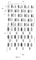
Links
Images









Classifications
-
- H—ELECTRICITY
- H10—SEMICONDUCTOR DEVICES; ELECTRIC SOLID-STATE DEVICES NOT OTHERWISE PROVIDED FOR
- H10K—ORGANIC ELECTRIC SOLID-STATE DEVICES
- H10K59/00—Integrated devices, or assemblies of multiple devices, comprising at least one organic light-emitting element covered by group H10K50/00
-
- H—ELECTRICITY
- H10—SEMICONDUCTOR DEVICES; ELECTRIC SOLID-STATE DEVICES NOT OTHERWISE PROVIDED FOR
- H10K—ORGANIC ELECTRIC SOLID-STATE DEVICES
- H10K59/00—Integrated devices, or assemblies of multiple devices, comprising at least one organic light-emitting element covered by group H10K50/00
- H10K59/10—OLED displays
- H10K59/12—Active-matrix OLED [AMOLED] displays
- H10K59/121—Active-matrix OLED [AMOLED] displays characterised by the geometry or disposition of pixel elements
-
- G—PHYSICS
- G09—EDUCATION; CRYPTOGRAPHY; DISPLAY; ADVERTISING; SEALS
- G09G—ARRANGEMENTS OR CIRCUITS FOR CONTROL OF INDICATING DEVICES USING STATIC MEANS TO PRESENT VARIABLE INFORMATION
- G09G3/00—Control arrangements or circuits, of interest only in connection with visual indicators other than cathode-ray tubes
- G09G3/20—Control arrangements or circuits, of interest only in connection with visual indicators other than cathode-ray tubes for presentation of an assembly of a number of characters, e.g. a page, by composing the assembly by combination of individual elements arranged in a matrix no fixed position being assigned to or needed to be assigned to the individual characters or partial characters
- G09G3/2007—Display of intermediate tones
- G09G3/2074—Display of intermediate tones using sub-pixels
-
- G—PHYSICS
- G07—CHECKING-DEVICES
- G07F—COIN-FREED OR LIKE APPARATUS
- G07F17/00—Coin-freed apparatus for hiring articles; Coin-freed facilities or services
- G07F17/32—Coin-freed apparatus for hiring articles; Coin-freed facilities or services for games, toys, sports, or amusements
- G07F17/3202—Hardware aspects of a gaming system, e.g. components, construction, architecture thereof
- G07F17/3204—Player-machine interfaces
- G07F17/3211—Display means
- G07F17/3213—Details of moving display elements, e.g. spinning reels, tumbling members
-
- G—PHYSICS
- G07—CHECKING-DEVICES
- G07F—COIN-FREED OR LIKE APPARATUS
- G07F17/00—Coin-freed apparatus for hiring articles; Coin-freed facilities or services
- G07F17/32—Coin-freed apparatus for hiring articles; Coin-freed facilities or services for games, toys, sports, or amusements
- G07F17/3202—Hardware aspects of a gaming system, e.g. components, construction, architecture thereof
- G07F17/3216—Construction aspects of a gaming system, e.g. housing, seats, ergonomic aspects
- G07F17/3218—Construction aspects of a gaming system, e.g. housing, seats, ergonomic aspects wherein at least part of the system is portable
-
- G—PHYSICS
- G07—CHECKING-DEVICES
- G07F—COIN-FREED OR LIKE APPARATUS
- G07F17/00—Coin-freed apparatus for hiring articles; Coin-freed facilities or services
- G07F17/32—Coin-freed apparatus for hiring articles; Coin-freed facilities or services for games, toys, sports, or amusements
- G07F17/3225—Data transfer within a gaming system, e.g. data sent between gaming machines and users
-
- G—PHYSICS
- G07—CHECKING-DEVICES
- G07F—COIN-FREED OR LIKE APPARATUS
- G07F17/00—Coin-freed apparatus for hiring articles; Coin-freed facilities or services
- G07F17/32—Coin-freed apparatus for hiring articles; Coin-freed facilities or services for games, toys, sports, or amusements
- G07F17/3244—Payment aspects of a gaming system, e.g. payment schemes, setting payout ratio, bonus or consolation prizes
-
- G—PHYSICS
- G07—CHECKING-DEVICES
- G07F—COIN-FREED OR LIKE APPARATUS
- G07F17/00—Coin-freed apparatus for hiring articles; Coin-freed facilities or services
- G07F17/32—Coin-freed apparatus for hiring articles; Coin-freed facilities or services for games, toys, sports, or amusements
- G07F17/326—Game play aspects of gaming systems
- G07F17/3267—Game outcomes which determine the course of the subsequent game, e.g. double or quits, free games, higher payouts, different new games
-
- G—PHYSICS
- G07—CHECKING-DEVICES
- G07F—COIN-FREED OR LIKE APPARATUS
- G07F17/00—Coin-freed apparatus for hiring articles; Coin-freed facilities or services
- G07F17/32—Coin-freed apparatus for hiring articles; Coin-freed facilities or services for games, toys, sports, or amusements
- G07F17/34—Coin-freed apparatus for hiring articles; Coin-freed facilities or services for games, toys, sports, or amusements depending on the stopping of moving members in a mechanical slot machine, e.g. "fruit" machines
-
- G—PHYSICS
- G09—EDUCATION; CRYPTOGRAPHY; DISPLAY; ADVERTISING; SEALS
- G09G—ARRANGEMENTS OR CIRCUITS FOR CONTROL OF INDICATING DEVICES USING STATIC MEANS TO PRESENT VARIABLE INFORMATION
- G09G3/00—Control arrangements or circuits, of interest only in connection with visual indicators other than cathode-ray tubes
- G09G3/20—Control arrangements or circuits, of interest only in connection with visual indicators other than cathode-ray tubes for presentation of an assembly of a number of characters, e.g. a page, by composing the assembly by combination of individual elements arranged in a matrix no fixed position being assigned to or needed to be assigned to the individual characters or partial characters
-
- H—ELECTRICITY
- H10—SEMICONDUCTOR DEVICES; ELECTRIC SOLID-STATE DEVICES NOT OTHERWISE PROVIDED FOR
- H10K—ORGANIC ELECTRIC SOLID-STATE DEVICES
- H10K59/00—Integrated devices, or assemblies of multiple devices, comprising at least one organic light-emitting element covered by group H10K50/00
- H10K59/10—OLED displays
- H10K59/12—Active-matrix OLED [AMOLED] displays
- H10K59/128—Active-matrix OLED [AMOLED] displays comprising two independent displays, e.g. for emitting information from two major sides of the display
-
- H—ELECTRICITY
- H10—SEMICONDUCTOR DEVICES; ELECTRIC SOLID-STATE DEVICES NOT OTHERWISE PROVIDED FOR
- H10K—ORGANIC ELECTRIC SOLID-STATE DEVICES
- H10K59/00—Integrated devices, or assemblies of multiple devices, comprising at least one organic light-emitting element covered by group H10K50/00
- H10K59/30—Devices specially adapted for multicolour light emission
- H10K59/35—Devices specially adapted for multicolour light emission comprising red-green-blue [RGB] subpixels
- H10K59/352—Devices specially adapted for multicolour light emission comprising red-green-blue [RGB] subpixels the areas of the RGB subpixels being different
-
- H—ELECTRICITY
- H10—SEMICONDUCTOR DEVICES; ELECTRIC SOLID-STATE DEVICES NOT OTHERWISE PROVIDED FOR
- H10K—ORGANIC ELECTRIC SOLID-STATE DEVICES
- H10K59/00—Integrated devices, or assemblies of multiple devices, comprising at least one organic light-emitting element covered by group H10K50/00
- H10K59/30—Devices specially adapted for multicolour light emission
- H10K59/35—Devices specially adapted for multicolour light emission comprising red-green-blue [RGB] subpixels
- H10K59/353—Devices specially adapted for multicolour light emission comprising red-green-blue [RGB] subpixels characterised by the geometrical arrangement of the RGB subpixels
-
- H—ELECTRICITY
- H10—SEMICONDUCTOR DEVICES; ELECTRIC SOLID-STATE DEVICES NOT OTHERWISE PROVIDED FOR
- H10K—ORGANIC ELECTRIC SOLID-STATE DEVICES
- H10K59/00—Integrated devices, or assemblies of multiple devices, comprising at least one organic light-emitting element covered by group H10K50/00
- H10K59/60—OLEDs integrated with inorganic light-sensitive elements, e.g. with inorganic solar cells or inorganic photodiodes
-
- G—PHYSICS
- G09—EDUCATION; CRYPTOGRAPHY; DISPLAY; ADVERTISING; SEALS
- G09G—ARRANGEMENTS OR CIRCUITS FOR CONTROL OF INDICATING DEVICES USING STATIC MEANS TO PRESENT VARIABLE INFORMATION
- G09G2300/00—Aspects of the constitution of display devices
- G09G2300/04—Structural and physical details of display devices
- G09G2300/0439—Pixel structures
- G09G2300/0452—Details of colour pixel setup, e.g. pixel composed of a red, a blue and two green components
-
- G—PHYSICS
- G09—EDUCATION; CRYPTOGRAPHY; DISPLAY; ADVERTISING; SEALS
- G09G—ARRANGEMENTS OR CIRCUITS FOR CONTROL OF INDICATING DEVICES USING STATIC MEANS TO PRESENT VARIABLE INFORMATION
- G09G2320/00—Control of display operating conditions
- G09G2320/02—Improving the quality of display appearance
- G09G2320/0233—Improving the luminance or brightness uniformity across the screen
-
- G—PHYSICS
- G09—EDUCATION; CRYPTOGRAPHY; DISPLAY; ADVERTISING; SEALS
- G09G—ARRANGEMENTS OR CIRCUITS FOR CONTROL OF INDICATING DEVICES USING STATIC MEANS TO PRESENT VARIABLE INFORMATION
- G09G2340/00—Aspects of display data processing
- G09G2340/04—Changes in size, position or resolution of an image
- G09G2340/0407—Resolution change, inclusive of the use of different resolutions for different screen areas
Definitions
- This disclosure relates to the field of display technologies, and particularly to a display substrate, a method for driving the same, a display apparatus, and a high-precision metal mask template.
- an all-screen panel with a high screen to panel ratio and an ultra-narrow bezel can greatly improve a visual effect over a general display panel, and thus has been widely favored.
- a front camera, an earphone, a fingerprint recognition area, a physical button, etc. are typically arranged on the front face of a display apparatus including an all-screen panel, e.g., a mobile phone, to photograph its user, to conduct a video session, to recognize a fingerprint, and to perform other functions.
- an all-screen panel e.g., a mobile phone
- An embodiment of this disclosure provides a display substrate including a display area including a first display sub-area and a second sub-area, wherein: a distribution density of pixels in the first display sub-area is higher than a distribution density of pixels in the second display sub-area.
- At least a part of sides of the second display sub-area coincide with at least a part of sides of the display area, and the other sides of the second display sub-area are surrounded by the first display sub-area.
- the first display sub-area and the second display sub-area are arranged in the row direction, or the first display sub-area and the second display sub-area are arranged in the column direction.
- the first display sub-area is arranged to surround the second display sub-area.
- the shape of the second display sub-area is one of a round, a drop shape, a rectangle, and a trapezia.
- the first display sub-area and the second display sub-area form a consecutive display area, and the shape of the display area is substantially a rectangle.
- the second display sub-area is located at a corner of the display area.
- the area of the second display sub-area is smaller than the area of the first display sub-area.
- the first display sub-area includes a plurality of first pixel elements and second pixel elements arranged adjacent to each other, wherein the first pixel elements include a first sub-pixel and a second sub-pixel, and the second pixel element includes a third sub-pixel and a second sub-pixel; and the second display sub-area includes a plurality of third pixel elements, and the third pixel elements include a first sub-pixel, a second sub-pixel, and a third sub-pixel arranged adjacent to each other.
- the sub-pixels in the second display sub-area are located in the same row as a part of the sub-pixels in the first display sub-area.
- the sub-pixels in the second display sub-area are located in the same column as a part of the sub-pixels in the first display sub-area.
- a light-emitting area of a first sub-pixel in the second display sub-area is not smaller than a light-emitting area of a first sub-pixel in the first display sub-area; a light-emitting area of a second sub-pixel in the second display sub-area is not smaller than a light-emitting area of a second sub-pixel in the first display sub-area; and a light-emitting area of a third sub-pixel in the second display sub-area is not smaller than a light-emitting area of a third sub-pixel in the first display sub-area.
- the plurality of third pixel elements are arranged in a matrix in the second display sub-area.
- the plurality of third pixel elements are arranged in a tessellated pattern in the second display sub-area.
- the first sub-pixel, the second sub-pixel, and the third sub-pixel in the third pixel element are arranged successively in the same row or column in the second display sub-area.
- the first sub-pixel and the third sub-pixel are arranged in the same row, and the second sub-pixel is located in an adjacent row to the row in which the first sub-pixel and the third sub-pixel are located.
- an orthographical projection of the center of the second sub-pixel onto a line connecting the center of the first sub-pixel with the center of the third sub-pixel lies between the center of the first sub-pixel, and the center of the third sub-pixel.
- the sub-pixels in two third pixel elements adjacent in the row direction are arranged in the same order in the row direction, and the sub-pixels in two third pixel elements adjacent in the column direction are arranged in opposite orders in the row direction.
- the sub-pixels in the third pixel elements in the second display sub-area are arranged in the same order.
- the sub-pixels in the third pixel elements in the same column are arranged in the same order; and the sub-pixels in the third pixel elements in two adjacent columns are arranged in opposite orders.
- the shapes of the first sub-pixels, the second sub-pixels, and the third sub-pixels are substantially the same in the second display sub-area.
- a light-emitting area of a second sub-pixel is smaller than or substantially equal to a light-emitting area of a first sub-pixel, and a light-emitting area of a second sub-pixel is smaller than or substantially equal to a light-emitting area of a third sub-pixel, in the second display sub-area.
- a light-emitting area of a first sub-pixel is substantially equal to a light-emitting area of a third sub-pixel in the second display sub-area.
- the first pixel elements and the second pixel elements are arranged alternately in the column direction, and the first pixel elements and the second pixel elements are arranged alternately in the row direction, in the first display sub-area.
- the second sub-pixel and the first sub-pixel in the first pixel elements are arranged in the same row, and the second sub-pixel and the third sub-pixel in the second pixel elements are arranged in the same row, in the first display sub-area; and for the first pixel element and the second pixel element adjacent in the row direction, the second sub-pixel in the first pixel element is not immediately adjacent to the second sub-pixel in the second pixel element.
- a light-emitting area of a first sub-pixel, a light-emitting area of a second sub-pixel, and a light-emitting area of a third sub-pixel are substantially the same in the first display sub-area.
- the second sub-pixel and the first sub-pixel in the first pixel elements are staggered in rows and columns, and the second sub-pixel and the third sub-pixel in the second pixel elements are arranged in the same row; and the first pixel element and the second pixel element adjacent in the column direction are a group of pixels, and in the same group of pixels, the second sub-pixel in the first pixel element, and the third sub-pixel in the second pixel element are arranged in the same row, and the second sub-pixel in the first pixel element, and the second sub-pixel in the second pixel element are located in the same column.
- a light-emitting area of a second sub-pixel is not larger than a light-emitting area of a first sub-pixel, and a light-emitting area of a second sub-pixel is not larger than a light-emitting area of a third sub-pixel, in the first display sub-area.
- two second sub-pixels in the same group of pixels are arranged adjacent to each other in the column direction, and the two second sub-pixels are arranged symmetric in the row direction.
- the shapes of the first sub-pixel and the third sub-pixel are substantially the same, and the shape of a combination of two second sub-pixels is substantially the same as the shape of the first sub-pixel, in the same group of pixels.
- the sub-pixels in the first pixel elements are arranged in the same order, and the sub-pixels in the second pixel elements are arranged in the same order, in the first display sub-area.
- the shape of at least one of a first sub-pixel and a third sub-pixel in the second display sub-area is substantially the same as the shape of a first sub-pixel in the first display sub-area.
- the shape of one of a first sub-pixel and a second sub-pixel in the first display sub-area is substantially the same as the shape of a second sub-pixel in the second display sub-area.
- the shape of the first sub-pixel is at least one of a rectangle and a hexagon.
- an embodiment of this disclosure further provides a display apparatus including the display substrate above.
- the display apparatus further includes a driver configured to drive the display substrate, wherein the driver is configured:
- an embodiment of this disclosure further provides a method for driving the display substrate, the method including: to drive the display substrate, the method including:
- determining for the sub-pixels in the first display sub-area the target grayscale of the sub-pixel includes:
- determining for the sub-pixels in the second display sub-area the target grayscale of the sub-pixel includes:
- an embodiment of this disclosure further provides a high-precision metal mask template for fabricating the display substrate above, wherein the high-precision metal mask template includes a plurality of opening areas corresponding in shape and position to the first sub-pixels, the second sub-pixels, or the third sub-pixels.
- the embodiments of this disclosure provide a display substrate, a method for driving the same, a display apparatus, and a high-precision metal mask template.
- a display substrate includes a display area including a first display sub-area A1 and a second sub-area A2, where a distribution density of pixels in the first display sub-area A1 is higher than a distribution density of pixels in the second display sub-area A2.
- the display area includes the first display sub-area in which pixels are distributed at a high density (e.g., a high resolution), and the second display sub-area in which pixels are distributed at a low density (e.g., a low resolution). Since the distribution density of pixels in the second display sub-area is lower, a camera and other elements can be arranged in the second display sub-display area, that is, the distribution density of the local pixels can be lowered to thereby improve the transmittivity of a screen so as to improve a screen to panel ratio of the display substrate.
- a high density e.g., a high resolution
- a low density e.g., a low resolution
- the distribution density of pixels can refer to the number of pixels arranged uniformly in a unit of area. If there are a large number of pixels arranged in a unit of area, then there will be a high distribution density of pixels, and thus a high resolution; and if there are a small number of pixels arranged in a unit of area, then there will be a low distribution density of pixels, and thus a low resolution.
- the number of second display sub-areas may be one or more; and the first display sub-area may be a consecutive area, or may be an inconsecutive area, dependent upon a real application environment, although an embodiment of the invention will not be limited thereto.
- the display substrate in the display substrate according to an embodiment of this disclosure, as illustrated in Fig. 1a to Fig. 1g , at least a part of sides of the second display sub-area A2 coincide with at least a part of sides of the display area, and the other sides of the second display sub-area A2 are surrounded by the first display sub-area A1, so that the second display sub-area A2 can be arranged at the edge of the display area.
- the first display sub-area A1 is arranged to surround the second display sub-area A2 so that the second display sub-area A2 can be arranged in the display area.
- the shape of the second display sub-area A2 can be arranged as a regular shape, and as illustrated in Fig. 1a to Fig. 1c , for example, the second display sub-area A2 can be arranged as a rectangle, where a top corner of the rectangle can be a right angle or can be an arc angle. As illustrated in Fig. Id, the second display sub-area A2 can be arranged as a trapezium, where a top corner of the trapezium can be a normal angle or can be an arc angle. As illustrated in Fig. 1h and Fig. 1i , the second display sub-area A2 can be arranged as a round.
- the shape of the second display sub-area A2 can be arranged as an irregular shape. As illustrated in Fig. 1e , for example, the second display sub-area A2 can be arranged as a drop shape.
- the shape of the second display sub-area can be designed according to the shape of an element arranged in the second display sub-area in a real application, although an embodiment of this disclosure will not be limited thereto.
- the first display sub-area A1 and the second display sub-area A2 form the consecutive display area
- the shape of the display area is substantially rectangular, so that the first display sub-area A1 and the second display sub-area A2 can be formed as complementary patterns to form the consecutive display area.
- the display area will be a rectangle, or if each top corner of the display area is an arc angle, then the shape of the display area will be substantially rectangular.
- a relative positional relationship between the first display sub-area and the second display sub-area, and their shapes will not be limited to any particular relative positional relationship and shapes, but can be arranged according to a screen design of the display substrate.
- the second display sub-area A2 can be arranged at the top-left corner of the first display sub-area A1 as illustrated in Fig. 1a .
- the second display sub-area A2 can be arranged at the top-right corner of the first display sub-area A1 as illustrated in Fig. 1b .
- the second display sub-area A2 can be arranged at the middle of the top of the first display sub-area A1 as illustrated in Fig.
- the first display sub-area A1 and the second display sub-area A2 can be arranged in the row direction as illustrated in Fig. 1f , where the second display sub-area A2 can be located above or below the first display sub-area A1.
- a sensor e.g., a sensor for recognizing a human face (e.g., an infrared sensor, etc.), can be further arranged in the second display sub-area A2.
- the first display sub-area A1 and the second display sub-area A2 can be arranged in the column direction as illustrated in Fig. 1g , where the second display sub-area A2 can be located to the left or right of first display sub-area A1.
- a sensor e.g., a sensor for recognizing a human face (e.g., an infrared sensor, etc.), can be further arranged in the second display sub-area A2.
- the second display sub-area A2 can be arranged at the center of the first display sub-area A1 as illustrated in Fig. 1h .
- the second display sub-area A2 can be arranged at a corner (e.g., the top-left corner) of the display area as illustrated in Fig. 1i .
- the particular position of the second display area A2 can be determined according to a real application environment in a real application, although an embodiment of the invention will not be limited thereto.
- the distribution density of pixels in the second display sub-area is determined according to an element arranged in the second display sub-area, and a display demand, although an embodiment of the invention will not be limited thereto.
- a camera is arranged in the second display sub-area, and if the distribution density of pixels is too high, then a good display effect will be guaranteed, but a definition of photographing may be degraded, or if the distribution density of pixels is too low, then a high definition of photographing will be guaranteed, but the display effect may be degraded.
- the distribution density of pixels in the second display sub-area is generally no lower than the distribution density of pixels in the first display sub-area by a factor of 1/4.
- the distribution density of pixels in the second display sub-area is 1/2, 1/3, or 1/4 of the distribution density of pixels in the first display sub-area.
- the ratio of the distribution density of pixels in the second display sub-area to the distribution density in the first display sub-area may be set smaller.
- the area of the second display sub-area A2 can be smaller than the area of the first display sub-area A1.
- the area of the second display sub-area can be designed according to an element arranged in the second display sub-area in a real application, although an embodiment of this disclosure will not be limited thereto.
- Pixel elements are generally arranged in the display area, and each pixel element includes a plurality of sub-pixels; and a pixel in an embodiment of this disclosure may refer to a combination of sub-pixels which can display an image at a pixel point independently, and for example, a pixel may refer to a pixel element.
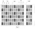
- the first display sub-area A1 includes a plurality of first pixel elements 10 and second pixel elements 20 arranged adjacent to each other, where each first pixel element 10 includes a first sub-pixel 1 and a second sub-pixel 2, and each second pixel element 20 includes a third sub-pixel 3 and a second sub-pixel 2.
- the number of pixels in the first display sub-area A1 is equal to the sum of the number of first pixel elements 10, and the number of second pixel elements 20, that is, the pixels are arranged in a pan tile pattern in the first display sub-area A1, and the image can be displayed at the pixel elements at a higher resolution than a physical resolution by borrowing the sub-pixels in their adjacent pixel elements.
- the second display sub-area A2 includes a plurality of third pixel elements 30, and each third pixel element 30 includes a first sub-pixel 1, a second sub-pixel 2, and a third sub-pixel 3 arranged adjacent to each other.
- the number of pixels in the second display sub-area A2 is equal to the number of third pixel elements 30, that is, a physical resolution of the pixels in the second display sub-area A2 is the display definition thereof.
- only an arrangement pattern of the third pixel elements 30 in the second display sub-area is illustrated, but a distribution density of the third pixel elements 30 in the second display sub-area A2 will not be limited to any particular distribution density.
- each pixel element can be a combination of sub-pixels at a pixel point, and for example, can be a combination of three, three, four or more of red, green, and blue sub-pixels, or each pixel element can be a combination of repeating elements or pixels, e.g., a combination of red, green, and blue sub-pixels.
- two adjacent pixel elements refer to two pixel elements between which there is not any other pixel element.
- Two adjacent sub-pixels refer to two sub-pixels between which there is not nay other sub-pixel.
- the arrangement of sub-pixels in the first display sub-area, and the arrangement of sub-pixels in the second display sub-area generally refer to the arrangements of sub-pixels inside the display sub-areas, and there may be a different arrangement of some sub-pixels at the edge of the display sub-area, although an embodiment of this disclosure will not be limited thereto.
- the first sub-pixels, the second sub-pixels, and the third sub-pixels are generally one of red, green, and blue sub-pixels respectively.
- the second sub-pixels are green sub-pixels
- the first sub-pixels are red or blue sub-pixels
- the third sub-pixels are blue or red sub-pixels.
- the sub-pixels in the second display sub-area A2 can be located in the same row as a part of the sub-pixels in the first display sub-area A1 so that the sub-pixels in the second display sub-area A2 correspond in row direction to the sub-pixels in the first display sub-area A1 instead of being arranged in a different row or column from the latter sub-pixels.
- the display substrate is fabricated in such a way that equivalently a part of the sub-pixels in the second display sub-area in a sub-pixel mask originally arranged regularly throughout the display area are removed, thus making it relatively easy to perform a fabrication process.
- the sub-pixels in the second display sub-area A2 can be located in the same column as a part of the sub-pixels in the first display sub-area A1 so that the sub-pixels in the second display sub-area A2 correspond in column direction to the sub-pixels in the first display sub-area A1 instead of being arranged in a different row or column from the latter sub-pixels.
- the display substrate is fabricated in such a way that a part of the sub-pixels in the second display sub-area in a sub-pixel mask originally arranged regularly throughout the display area are removed, thus making it relatively easy to perform a fabrication process. As illustrated in Fig.
- a light-emitting area of a first sub-pixel 1 in the second display sub-area A2 is substantially equal to a light-emitting area of a first sub-pixel 1 in the first display sub-area A1
- a light-emitting area of a third sub-pixel 3 in the second display sub-area A2 is substantially equal to a light-emitting area of a third sub-pixel 3 in the first display sub-area A1.
- a light-emitting area of a second sub-pixel 2 in the second display sub-area A2 is substantially equal to a light-emitting area of a second sub-pixel 2 in the first display sub-area A1.
- the distribution density of pixels in the second display sub-area is lower than the distribution density of pixels in the first display sub-area, so in order to display an image, brightness in the second distribution density of pixels is lower than brightness in the first distribution density of pixels so that there may be an apparent dark strip visible to human eyes, at the interface between the first display sub-area and the second display sub-area.
- brightness in the second distribution density of pixels is lower than brightness in the first distribution density of pixels so that there may be an apparent dark strip visible to human eyes, at the interface between the first display sub-area and the second display sub-area.
- a light-emitting area of a first sub-pixel 1 in the second display sub-area A2 is larger than a light-emitting area of a first sub-pixel 1 in the first display sub-area A1
- a light-emitting area of a second sub-pixel 2 in the second display sub-area A2 is larger than a light-emitting area of a second sub-pixel 2 in the first display sub-area A1
- a light-emitting area of a third sub-pixel 1 in the second display sub-area A2 is larger than a light-emitting area of a third sub-pixel 1 in the first display sub-area A1, that is, the light-emitting areas of the sub-pixels in the second display sub-area A2 can be increased to thereby lower the difference in brightness between the second display sub-area A2 and the first display sub-area A1 so as to alleviate the dark strip at the interface between the second display sub-area A2 and the first display sub-area A1.
- a plurality of third pixel elements 30 are arranged in a matrix in the second display sub-area A2 as illustrated in Fig. 2 to Fig. 5 , and Fig. 7 to Fig. 10 .
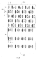
- a plurality of third pixel elements 30 are arranged in a tessellated pattern in the second display sub-area A2 as illustrated in Fig. 6 , and Fig. 11 to Fig. 13 , that is, the third pixel elements 30 are arranged in every other column in the row direction, and in every other row in the column direction.
- the third pixel elements 30 in the odd rows are arranged in the odd columns
- the third pixel elements 30 in the even rows are arranged in the even rows, so that the third pixel elements 30 are distributed uniformly in both the row direction and the column direction, thus resulting in uniform brightness in the second display sub-area A2.
- the third pixel elements 30 in the odd rows can be arranged in the even columns, and the third pixel elements 30 in the even rows can be arranged in the odd columns, so that any two third pixel elements are spaced from each other by a specific spacing, where for example, the spacing can be the length of at least one third pixel element in the row direction, and the length of at least one third pixel element in the column direction, although an embodiment of this disclosure will not be limited thereto.
- each third pixel element 30 in the second display sub-area A2 in each third pixel element 30 in the second display sub-area A2, the first sub-pixel 1 and the third sub-pixel 3 are arranged in the same row, and the second sub-pixel 2 is located in an adjacent row to the row in which the first sub-pixel 1 and the third sub-pixel 3 are located.
- first sub-pixel 1 and the third sub-pixel 3 in the same third pixel element 30 are located in the first row, and the second sub-pixel 2 is located in the second row, so that lines connecting the centers of the first sub-pixel, the second sub-pixel, and the third sub-pixel in the same third pixel element 30 constitute a triangle to thereby avoid traverse bright and dark strips from occurring in the second display sub-area.
- the center of a sub-pixel refers to the center of a light-emitting area of the sub-pixel.
- a sub-pixel generally includes an anode layer, a light-emitting layer, and a cathode layer structured in a stack, where in order to display an image, the light-emitting area corresponding to the stack structure is a light-emitting area of the sub-pixel, so that the area occupied by the light-emitting area is a light-emitting area.
- the light-emitting area can alternatively be an area occupied by an opening area defined by the pixel definition layer, for example, although an embodiment of this disclosure will not be limited thereto.
- an orthographical projection of the center of the second sub-pixel 2 onto the line L1 connecting the center of the first sub-pixel 1 with the center of the third sub-pixel 3 lies between the center of the first sub-pixel 1, and the center of the third sub-pixel 3.
- the orthographical projection of the center of the second sub-pixel 2 onto the line L1 connecting the center of the first sub-pixel 1 with the center of the third sub-pixel 3 lies onto the intersection between the connecting line L1 and the straight line L2.
- the distance between the center of the second sub-pixel 2, and the center of the first sub-pixel 1 in the third pixel element 30 can be equal to the distance between the center of the second sub-pixel 2, and the center of the third sub-pixel 3 so that these three sub-pixels are arranged in an isoceles triangle pattern to thereby avoid vertical bright and dark strips from occurring in the second display sub-area A2.
- the distance between the center of the second sub-pixel 2, and the center of the first sub-pixel 1 may not be exactly equal to the distance between the center of the second sub-pixel 2, and the center of the third sub-pixel 3, and there may be some error due to a limiting process condition or another factor, e.g., an arrangement of wires or through-holes, in a real process, so the shapes and the positions of the respective sub-pixels, and their relative positional relationship can substantially satisfy the condition above without departing from the scope of this disclosure.
- the first sub-pixel 1, the second sub-pixel 2, and the third sub-pixel 3 in the third pixel element 30 are arranged in the same row or column in the second display sub-area A2, although an embodiment of this disclosure will not be limited thereto.
- the first sub-pixel 1, the second sub-pixel 2, and the third sub-pixel 3 in the third pixel element 30 are arranged successively in the same row or column in the second display sub-area A2, although an embodiment of this disclosure will not be limited thereto.
- the display substrate according to an embodiment of this disclosure as illustrated in Fig. 2 to Fig. 4 , Fig. 6 to Fig. 9 , and Fig. 11 to Fig. 13 , the first sub-pixel 1, the second sub-pixel 2, and the third sub-pixel 3 in the third pixel element 30 are arranged successively in the same row or column in the second display sub-area A2, although an embodiment of this disclosure will not be limited thereto.
- the display substrate according to an embodiment of this disclosure as illustrated in Fig. 2 to Fig. 4 , Fig. 6 to Fig. 9 , and Fig. 11 to Fig.
- the first sub-pixel 1, the second sub-pixel 2, and the third sub-pixel 3 in the third pixel element 30 are arranged adjacent to each other in order in the same row or column in the second display sub-area A2, although an embodiment of this disclosure will not be limited thereto.
- the sub-pixels in two third pixel elements 30 adjacent in the row direction are arranged in the same order in the row direction, and the sub-pixels in two third pixel elements 30 adjacent in the column direction are arranged in opposite orders in the row direction, so that the first sub-pixels 1 and the third sub-pixels 3 can be arranged alternately in the column direction in the second display sub-area A2 to thereby avoid a color crosstalk from occurring in the column direction.
- the sub-pixels in two third pixel elements 30 adjacent in the row direction are arranged in the same order in the row direction
- the sub-pixels in two third pixel elements 30 adjacent in the column direction are arranged in opposite orders in the row direction, so that the first sub-pixels 1 and the third sub-pixels 3 can be arranged alternately in the column direction in the second display sub-area A2 to thereby avoid a color crosstalk from occurring in the column direction.
- the first sub-pixel 1, the second sub-pixel 2, and the third sub-pixel 3 in each of two adjacent third pixel elements 30 are arranged successively from the left to the right in the row direction.
- the first column of third pixel elements 30 as an example, in the column direction, the first sub-pixel 1, the second sub-pixel 2, and the third sub-pixel 3 in each third pixel element 30 in an odd row are arranged successively from the left to the right, and the first sub-pixel 1, the second sub-pixel 2, and the third sub-pixel 3 in each third pixel element 30 in an even row are arranged successively from the left to the right.
- the first sub-pixel 1, the second sub-pixel 2, and the third sub-pixel 3 in each third pixel element 30 in an even row are arranged successively from the left to the right.
- the first sub-pixel 1, the second sub-pixel 2, and the third sub-pixel 3 in each of two adjacent third pixel elements 30 are arranged in an upside-down triangle pattern in the row direction.
- the first column of third pixel elements 30 as an example, in the column direction, the first sub-pixel 1, the second sub-pixel 2, and the third sub-pixel 3 in each third pixel element 30 in an odd row are arranged in an upside-down triangle patter, and the first sub-pixel 1, the second sub-pixel 2, and the third sub-pixel 3 in each third pixel element 30 in an even row are arranged in an upside-down triangle patter.
- the sub-pixels in each third pixel element in the second display sub-area A2 can be arranged in the same order as illustrated in Fig. 2 , and Fig. 7 to Fig. 11 .
- the sub-pixels in each third pixel element 30 in the same column are arranged in the same order, and the sub-pixels in the third pixel elements 30 in two adjacent columns are arranged in opposite orders, in the second display sub-area A2 as illustrated in Fig. 13 .
- the first sub-pixel 1, the second sub-pixel 2, and the third sub-pixel 3 in each third pixel element 30 in an odd column are arranged successively from the left to the right
- the second sub-pixel 2 and the third sub-pixel 3 in each third pixel element 30 in an even column are arranged successively from the left to the right.
- the shapes of the first sub-pixels 1, the second sub-pixels 2, and the third sub-pixels 3 are substantially the same in the second display sub-area A2 as illustrated in Fig. 2 to Fig. 6 , and Fig. 8 to Fig. 13 .
- a light-emitting area of a second sub-pixel is smaller than or substantially equal to a light-emitting area of a first sub-pixel, and a light-emitting area of a second sub-pixel is smaller than or substantially equal to a light-emitting area of a third sub-pixel, in the second display sub-area.
- a light-emitting area of a second sub-pixel 2 is substantially equal to a light-emitting area of a first sub-pixel 1
- a light-emitting area of a second sub-pixel 2 is substantially equal to a light-emitting area of a third sub-pixel 3, in the second display sub-area A2.
- a light-emitting area of a second sub-pixel 2 is smaller than to a light-emitting area of a first sub-pixel 1
- a light-emitting area of a second sub-pixel 2 is smaller than or substantially equal to a light-emitting area of a third sub-pixel 3, in the second display sub-area.
- a light-emitting area of a second sub-pixel a light-emitting area of a first sub-pixel
- a light-emitting area of a third sub-pixel in the second display sub-area can be determined according to a real application, although an embodiment of this disclosure will not be limited thereto.
- a light-emitting area of a first sub-pixel 1 is substantially equal to a light-emitting area of a third sub-pixel 3 in the second display sub-area A2.
- the first pixel elements 10 and the second pixel elements 20 in the first display sub-area A1 can be arranged in any pan tile pattern, although an embodiment of this disclosure will not be limited thereto.
- the first pixel elements 10 and the second pixel elements 20 are arranged alternately in the column direction, and the first pixel elements 10 and the second pixel elements 20 are arranged alternately in the row direction, in the first display sub-area A1.
- the second sub-pixel 2 and the first sub-pixel 1 in each first pixel element 10 are arranged in the same row, and the second sub-pixel 2 and the third sub-pixel 3 in each second pixel element 20 are arranged in the same row, in the first display sub-area A1; and for the first pixel element 10 and the second pixel element 20 adjacent in the row direction, the second sub-pixel 2 in the first pixel element 10 is not immediately adjacent to the second sub-pixel 2 in the second pixel element 20.
- the second sub-pixel 2 in the first pixel element 10 is spaced from the second sub-pixel 2 in the second pixel element 20 by the third sub-pixel 3.
- the third sub-pixel 3 may be alternative implementations to the implementation above, and a repeated description thereof will be omitted here.
- a light-emitting area of a first sub-pixel 1, a light-emitting area of a second sub-pixel 2, and a light-emitting area of a third sub-pixel 3 can be substantially the same in the first display sub-area A2.
- the second sub-pixel 2 and the first sub-pixel 1 in each first pixel element 10 are staggered in rows and columns, and the second sub-pixel 2 and the third sub-pixel 3 in each second pixel element 20 are arranged in the same row, in the first display sub-area A1; and the first pixel element 10 and the second pixel element 20 adjacent in the column direction are a group of pixels 100, and in the same group of pixels 100, the second sub-pixel 2 in the first pixel element 10, and the third sub-pixel 3 in the second pixel element 20 are arranged in the same row, and the second sub-pixel 2 in the first pixel element 10, and the second sub-pixel 2 in the second pixel element 20 are located in the same column.
- two second sub-pixels 2 in the same group of pixels 100 are arranged adjacent to each other in the column direction, and the two second sub-pixels 2 are symmetric in the row direction even if they are arranged in a mirror pattern.
- the total light-emitting area of two second sub-pixels 2 is smaller than a light-emitting area of a first sub-pixel 1
- the total light-emitting area of two second sub-pixels 2 is smaller than a light-emitting area of a third sub-pixel 3, because the green sub-pixels have higher light-emission efficiency than that of the sub-pixels in the other colors.
- the sub-pixels in each first pixel element 10 are arranged in the same order, and the sub-pixels in each second pixel element 20 are arranged in the same order, in the first display sub-area.
- the first sub-pixel 1 and the second sub-pixel 2 in each first pixel element 10 are arranged successively from the left to the right, and the third sub-pixel 3 and the second sub-pixel 2 in each second pixel element 20 are arranged successively from the left to the right.
- the second sub-pixel 2 and the third sub-pixel 3 in each second pixel element 20 are arranged successively from the left to the right, and the first sub-pixel 1 and the second sub-pixel 2 in each first pixel element 10 are arranged successively from the top left to the bottom right.
- a light-emitting area of a second sub-pixel is not larger than a light-emitting area of a first sub-pixel, and a light-emitting area of a second sub-pixel is not larger than a light-emitting area of a third sub-pixel, in the first display sub-area.
- a light-emitting area of a second sub-pixel 2 is substantially equal to a light-emitting area of a first sub-pixel 1
- a light-emitting area of a second sub-pixel 2 is substantially equal to a light-emitting area of a third sub-pixel 3, in the first display sub-area A1.
- a light-emitting area of a second sub-pixel 2 is smaller than a light-emitting area of a first sub-pixel 1, and a light-emitting area of a second sub-pixel 2 is smaller than a light-emitting area of a third sub-pixel 3, in the first display sub-area A1. Since the number of first sub-pixels 1 is the same as the number of third sub-pixels 3, and the number of second sub-pixels 2 is twice the number of first sub-pixels 1, in the first display sub-area A1, the light-emitting area of each second sub-pixel 2 can be made smaller.
- a light-emitting area of a first sub-pixel 1 is substantially equal to a light-emitting area of a third sub-pixel 3 in the first display sub-area A1 as illustrated in Fig. 2 to Fig. 13 .
- the shapes of the first sub-pixels, the second sub-pixels, and the third sub-pixels in the first display sub-area will not be limited to any particular shapes, and may be regular or irregular shapes.
- a regular shape is generally easy to form from the perspective of a process.
- the shapes of the first sub-pixels, the second sub-pixels, and the third sub-pixels in the second display sub-area will not be limited to any particular shapes, and may be regular or irregular shapes.
- a regular shape is generally easy to form from the perspective of a process.
- the shapes of the first sub-pixel 1 and the third sub-pixel 3 are the same, and the shape of a combination of two second sub-pixels 2 is the same as the shape of the first sub-pixel 1 or the third sub-pixel 3, in the same group of pixels 100.
- the shape of a first sub-pixel is at least one of a rectangle and a hexagon. As illustrated in Fig. 2 to Fig. 6 , for example, the shape of a first sub-pixel 1 in each of the first display sub-area A1 and the second display sub-area A2 is rectangular. As illustrated in Fig. 7 to Fig.
- the shape of a first sub-pixel 1 in each of the first display sub-area A1 and the second display sub-area A2 is hexagonal.
- the shape of a first sub-pixel can alternatively be a rounded shape, elliptic, etc., although an embodiment of this disclosure will not be limited thereto.
- both of the shapes of the first sub-pixels 1 and the third sub-pixels 3 are hexagonal, and the shape of a combination of two sub-pixels 2 is hexagonal, in the first display sub-area A1.
- the shape of at least one of a first sub-pixel and a third sub-pixel in the second display sub-area is substantially the same as the shape of a first sub-pixel in the first display sub-area.
- the shape of a first sub-pixel 1 in the second display sub-area A2 is substantially the same as the shape of a first sub-pixel 1 in the first display sub-area A1.
- the shape of a third sub-pixel 3 in the second display sub-area A2 is substantially the same as the shape of a first sub-pixel 1 in the first display sub-area A1.
- Fig. 2 to Fig. 13 the shape of a third sub-pixel 3 in the second display sub-area A2 is substantially the same as the shape of a first sub-pixel 1 in the first display sub-area A1.
- the shape of a first sub-pixel 1, and the shape of a third sub-pixel 3 respectively in the second display sub-area A2 are substantially the same as the shape of a first sub-pixel 1 in the first display sub-area A1.
- the shape of one of a first sub-pixel and a second sub-pixel in the first display sub-area is substantially the same as the shape of a second sub-pixel in the second display sub-area.
- the shape of a first sub-pixel 1 in the first display sub-area A1 is substantially the same as the shape of a second sub-pixel 2 in the second display sub-area A2.
- the shape of a second sub-pixel 2 in the first display sub-area A1 is substantially the same as the shape of a second sub-pixel 2 in the second display sub-area A2.
- the shapes of the respective first sub-pixels 1, the respective second sub-pixels 2, and the respective third sub-pixels 3 in the same sub-area are substantially the same, and although there is substantially the same shape of these three kinds of sub-pixels, there may be different light-emitting areas thereof.
- a light-emitting area of a second sub-pixel 2 is smaller than a light-emitting area of a first sub-pixel 1
- a light-emitting area of a second sub-pixel 2 is smaller than a light-emitting area of a third sub-pixel 3, in the second display sub-area A2.
- a light-emitting area of a blue sub-pixel is larger than a light-emitting area of a red sub-pixel, which is larger than a light-emitting area of a green sub-pixel, or a light-emitting area of a blue sub-pixel is larger than a light-emitting area of a green sub-pixel, which is larger than a light-emitting area of a red sub-pixel, although an embodiment of this disclosure will not be limited thereto.
- the shape of a sub-pixel refers to the shape of a light-emitting area of the sub-pixel.
- the total light-emitting area of two second sub-pixels 2 is smaller than the area of a first sub-pixel 1
- the total light-emitting area of two second sub-pixels 2 is smaller than the area of a third sub-pixel 3, because the green sub-pixels have higher light-emission efficiency than that of the sub-pixels in the other colors.
- a light-emitting area of a second sub-pixel 2 is smaller than a light-emitting area of a first sub-pixel 1
- a light-emitting area of a second sub-pixel is smaller than a light-emitting area of a third sub-pixel 3.
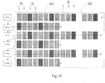
- the display substrate according to an embodiment of this disclosure generally displays an image by scanning the first display sub-area row by row. As illustrated in Fig. 15 , for example, when the first display sub-area A1 and the second display sub-area A2 are adjacent to each other in the row direction, gate driver circuits GOA1 to GOA5 output signals row by row, but only the GOA1, the GOA3, and the GOA5 output signals for the second display sub-area A2.
- an embodiment of this disclosure further provides a method for driving the display substrate according to any one of an embodiments above of this disclosure, and as illustrated in Fig. 14 , the method includes the following steps:
- a target grayscale of the sub-pixel is generally an initial grayscale thereof; and when the number of physical pixels in the first display sub-area is less than the number of pixels in the image data, there is a borrowing relationship between displaying sub-pixels, so a sub-pixel may correspond to two or more pixels in the image data, and thus the garget grayscale of the sub-pixel shall be calculated according to the initial grayscale of the sub-pixel in the raw image data, corresponding thereto.
- a physical pixel corresponds to a pixel in the image data, and a target grayscale of the sub-pixel is generally an initial grayscale thereof.
- a target grayscale of the sub-pixel is generally an initial grayscale thereof.
- a driver adjusts the grayscale of the sub-pixel in the second display sub-area according to a light-emitting area of the sub-pixel, and the distribution density of pixels in the second display sub-area. For example, if there is a larger light-emitting area of the sub-pixel, there is high overall brightness in the second display sub-area, and there are a larger number of sub-pixels distributed in the second display sub-area, then there will be high overall brightness in the second display sub-area.
- a physical pixel generally includes three RGB sub-pixels.
- both the first sub-pixels and the third sub-pixels are borrowed for displaying an image, so a first sub-pixel generally corresponds to two pixels in the image data, a third sub-pixel corresponds to two pixels in the image data, and no second sub-pixel is borrowed, and thus a second sub-pixel generally corresponds to a pixel in the image data.
- determining for each sub-pixel in the first display sub-area the target grayscale of the sub-pixel particularly can include:
- brightness in the second display sub-area can be adjusted as appropriate, where the brightness is in proportion to a light-emitting area and the distribution density of pixels.
- determining for each sub-pixel in the second display sub-area the target grayscale of the sub-pixel particularly can include:
- the error adjustment coefficient k can be adjusted according to a real display effect of the display substrate, although an embodiment of this disclosure will not be limited thereto.
- X k ⁇ s ⁇ ⁇ ⁇ x i , where x1 represents an initial grayscale of any one of the four sub-pixels.
- X k ⁇ s ⁇ ⁇ x 1 Gamma + x 2 Gamma 2 1 Gamma , where x1 and x2 represent initial grayscales of any two of the four sub-pixels.
- X k ⁇ s ⁇ ⁇ x 1 Gamma + x 2 Gamma + x 3 Gamma 3 1 Gamma , where x1, x2, and x3 represent initial grayscales of any three of the four sub-pixels.
- X k ⁇ s ⁇ ⁇ x 1 Gamma + x 2 Gamma + x 3 Gamma + x 4 Gamma 4 1 Gamma , where x1, x2, x3, and x4 represent initial grayscales of the four sub-pixels.
- an embodiment of this disclosure further provides a display apparatus including the display substrate according to any one of the embodiments above of this disclosure.
- the display apparatus can be a mobile phone, a tablet computer, a TV set, a monitor, a notebook computer, a digital photo frame, a navigator, or any other product or component with a display function.
- the display apparatus further includes a driver configured to drive the display substrate, where the driver of the display substrate can be an Integrated Circuit (IC), an external Central Processing Unit (CPU), a micro processor, etc., and is configured:
- IC Integrated Circuit
- CPU Central Processing Unit
- micro processor etc.
- the driver is configured to determine for each sub-pixel in the first display sub-area the target grayscale of the sub-pixel by:
- brightness in the second display sub-area can be adjusted as appropriate, where the brightness is in proportion to a light-emitting area and the distribution density of pixels.
- the driver is configured to determine for each sub-pixel in the second display sub-area the target grayscale of the sub-pixel by:
- the error adjustment coefficient k can be adjusted according to a real display effect of the display substrate, although an embodiment of this disclosure will not be limited thereto.
- the driver integrates all the algorithms for calculating the target grayscales of the sub-pixels in the respective sub-areas into an IC.
- the driver determines the target grayscales corresponding to the respective sub-pixels according to the received image data.
- Demura algorithm Furthermore before the display substrates displays at the target grayscales, in order to improve the uniformity of brightness, generally a Demura algorithm shall also be performed. A particular Demura algorithm is known in the art, so a repeated description thereof will be omitted here.
- an embodiment of this disclosure further provides a high-precision metal mask template for fabricating the display substrate according to any one of an embodiments of this disclosure, where the high-precision metal mask template includes a plurality of opening areas corresponding in shape and position to the first sub-pixels, the second sub-pixels, or the third sub-pixels.
- each sub-pixel generally includes an anode layer, a light-emitting layer, and a cathode layer, where the light-emitting layer is generally vapor-plated using the high-precision metal mask template above.
- the high-precision metal mask template for forming the first sub-pixels includes opening areas 01 corresponding in shape and position to the light-emitting layers of the first substrate 1 in the display substrate as illustrated in Fig. 16 .
- the area of an opening area 01 is generally larger than an area of a corresponding light-emitting area due to a limiting process factor.
- the display area includes the first display sub-area with a high distribution density of pixels (i.e., a high resolution), and the second display sub-area with a low distribution density of pixels (i.e., a low resolution), and since the distribution density of pixels in the second display sub-area is low, a camera and another element can be arranged in the second display sub-area, that is, the distribution density of the local pixels can be lowered to thereby improve the transmittivity of a screen so as to improve a screen to panel ratio of the display substrate.
- a high distribution density of pixels i.e., a high resolution
- the second display sub-area with a low distribution density of pixels i.e., a low resolution
- the grayscale of a sub-pixel in the second display sub-area can be adjusted according to the light-emitting area of the sub-pixel, and the distribution density of pixels, in the second display sub-area to thereby compensate for a significant difference in brightness between the second display sub-area and the first display sub-area due to the difference between the distribution density of pixels in the first display sub-area, and the distribution density of pixels in the second display sub-area so as to alleviate a dark strip from occurring at the interface between the first display sub-area and the second display sub-area, so that the image can be displayed throughout the screen.
Landscapes
- Physics & Mathematics (AREA)
- Engineering & Computer Science (AREA)
- General Physics & Mathematics (AREA)
- Microelectronics & Electronic Packaging (AREA)
- Geometry (AREA)
- Computer Hardware Design (AREA)
- Theoretical Computer Science (AREA)
- Chemical & Material Sciences (AREA)
- Life Sciences & Earth Sciences (AREA)
- Inorganic Chemistry (AREA)
- Sustainable Development (AREA)
- Electroluminescent Light Sources (AREA)
- Devices For Indicating Variable Information By Combining Individual Elements (AREA)
- Control Of El Displays (AREA)
- Physical Vapour Deposition (AREA)
- Control Of Indicators Other Than Cathode Ray Tubes (AREA)
Abstract
Description
- This application claims the benefits of Chinese Patent Application No.
201810639832.6 - This disclosure relates to the field of display technologies, and particularly to a display substrate, a method for driving the same, a display apparatus, and a high-precision metal mask template.
- As the display technologies are developing, an all-screen panel with a high screen to panel ratio and an ultra-narrow bezel can greatly improve a visual effect over a general display panel, and thus has been widely favored. At present, a front camera, an earphone, a fingerprint recognition area, a physical button, etc., are typically arranged on the front face of a display apparatus including an all-screen panel, e.g., a mobile phone, to photograph its user, to conduct a video session, to recognize a fingerprint, and to perform other functions. However the arrangement of these indispensable functional elements may hinder a screen to panel ratio from being improved.
- An embodiment of this disclosure provides a display substrate including a display area including a first display sub-area and a second sub-area, wherein:
a distribution density of pixels in the first display sub-area is higher than a distribution density of pixels in the second display sub-area. - Optionally in an embodiment of this disclosure, at least a part of sides of the second display sub-area coincide with at least a part of sides of the display area, and the other sides of the second display sub-area are surrounded by the first display sub-area.
- Optionally in an embodiment of this disclosure, the first display sub-area and the second display sub-area are arranged in the row direction, or the first display sub-area and the second display sub-area are arranged in the column direction.
- Optionally in an embodiment of this disclosure, the first display sub-area is arranged to surround the second display sub-area.
- Optionally in an embodiment of this disclosure, the shape of the second display sub-area is one of a round, a drop shape, a rectangle, and a trapezia.
- Optionally in an embodiment of this disclosure, the first display sub-area and the second display sub-area form a consecutive display area, and the shape of the display area is substantially a rectangle.
- Optionally in an embodiment of this disclosure, the second display sub-area is located at a corner of the display area.
- Optionally in an embodiment of this disclosure, the area of the second display sub-area is smaller than the area of the first display sub-area.
- Optionally in an embodiment of this disclosure, the first display sub-area includes a plurality of first pixel elements and second pixel elements arranged adjacent to each other, wherein the first pixel elements include a first sub-pixel and a second sub-pixel, and the second pixel element includes a third sub-pixel and a second sub-pixel; and the second display sub-area includes a plurality of third pixel elements, and the third pixel elements include a first sub-pixel, a second sub-pixel, and a third sub-pixel arranged adjacent to each other.
- Optionally in an embodiment of this disclosure, the sub-pixels in the second display sub-area are located in the same row as a part of the sub-pixels in the first display sub-area. Optionally in an embodiment of this disclosure, the sub-pixels in the second display sub-area are located in the same column as a part of the sub-pixels in the first display sub-area.
- Optionally in an embodiment of this disclosure, a light-emitting area of a first sub-pixel in the second display sub-area is not smaller than a light-emitting area of a first sub-pixel in the first display sub-area;
a light-emitting area of a second sub-pixel in the second display sub-area is not smaller than a light-emitting area of a second sub-pixel in the first display sub-area; and a light-emitting area of a third sub-pixel in the second display sub-area is not smaller than a light-emitting area of a third sub-pixel in the first display sub-area. - Optionally in an embodiment of this disclosure, the plurality of third pixel elements are arranged in a matrix in the second display sub-area.
- Optionally in an embodiment of this disclosure, the plurality of third pixel elements are arranged in a tessellated pattern in the second display sub-area.
- Optionally in an embodiment of this disclosure, the first sub-pixel, the second sub-pixel, and the third sub-pixel in the third pixel element are arranged successively in the same row or column in the second display sub-area.
- Optionally in an embodiment of this disclosure, in the third pixel element in the second display sub-area, the first sub-pixel and the third sub-pixel are arranged in the same row, and the second sub-pixel is located in an adjacent row to the row in which the first sub-pixel and the third sub-pixel are located.
- Optionally in an embodiment of this disclosure, in the same third pixel element, an orthographical projection of the center of the second sub-pixel onto a line connecting the center of the first sub-pixel with the center of the third sub-pixel lies between the center of the first sub-pixel, and the center of the third sub-pixel.
- Optionally in an embodiment of this disclosure, in the second display sub-area, the sub-pixels in two third pixel elements adjacent in the row direction are arranged in the same order in the row direction, and the sub-pixels in two third pixel elements adjacent in the column direction are arranged in opposite orders in the row direction.
- Optionally in an embodiment of this disclosure, the sub-pixels in the third pixel elements in the second display sub-area are arranged in the same order.
- Optionally in an embodiment of this disclosure, in the second display sub-area, the sub-pixels in the third pixel elements in the same column are arranged in the same order; and
the sub-pixels in the third pixel elements in two adjacent columns are arranged in opposite orders. - Optionally in an embodiment of this disclosure, the shapes of the first sub-pixels, the second sub-pixels, and the third sub-pixels are substantially the same in the second display sub-area.
- Optionally in an embodiment of this disclosure, a light-emitting area of a second sub-pixel is smaller than or substantially equal to a light-emitting area of a first sub-pixel, and a light-emitting area of a second sub-pixel is smaller than or substantially equal to a light-emitting area of a third sub-pixel, in the second display sub-area.
- Optionally in an embodiment of this disclosure, a light-emitting area of a first sub-pixel is substantially equal to a light-emitting area of a third sub-pixel in the second display sub-area.
- Optionally in an embodiment of this disclosure, the first pixel elements and the second pixel elements are arranged alternately in the column direction, and the first pixel elements and the second pixel elements are arranged alternately in the row direction, in the first display sub-area.
- Optionally in an embodiment of this disclosure, the second sub-pixel and the first sub-pixel in the first pixel elements are arranged in the same row, and the second sub-pixel and the third sub-pixel in the second pixel elements are arranged in the same row, in the first display sub-area; and
for the first pixel element and the second pixel element adjacent in the row direction, the second sub-pixel in the first pixel element is not immediately adjacent to the second sub-pixel in the second pixel element. - Optionally in an embodiment of this disclosure, a light-emitting area of a first sub-pixel, a light-emitting area of a second sub-pixel, and a light-emitting area of a third sub-pixel are substantially the same in the first display sub-area.
- Optionally in an embodiment of this disclosure, the second sub-pixel and the first sub-pixel in the first pixel elements are staggered in rows and columns, and the second sub-pixel and the third sub-pixel in the second pixel elements are arranged in the same row; and the first pixel element and the second pixel element adjacent in the column direction are a group of pixels, and in the same group of pixels, the second sub-pixel in the first pixel element, and the third sub-pixel in the second pixel element are arranged in the same row, and the second sub-pixel in the first pixel element, and the second sub-pixel in the second pixel element are located in the same column.
- Optionally in an embodiment of this disclosure, a light-emitting area of a second sub-pixel is not larger than a light-emitting area of a first sub-pixel, and a light-emitting area of a second sub-pixel is not larger than a light-emitting area of a third sub-pixel, in the first display sub-area.
- Optionally in an embodiment of this disclosure, two second sub-pixels in the same group of pixels are arranged adjacent to each other in the column direction, and the two second sub-pixels are arranged symmetric in the row direction.
- Optionally in an embodiment of this disclosure, the shapes of the first sub-pixel and the third sub-pixel are substantially the same, and the shape of a combination of two second sub-pixels is substantially the same as the shape of the first sub-pixel, in the same group of pixels.
- Optionally in an embodiment of this disclosure, the sub-pixels in the first pixel elements are arranged in the same order, and the sub-pixels in the second pixel elements are arranged in the same order, in the first display sub-area.
- Optionally in an embodiment of this disclosure, the shape of at least one of a first sub-pixel and a third sub-pixel in the second display sub-area is substantially the same as the shape of a first sub-pixel in the first display sub-area.
- Optionally in an embodiment of this disclosure, the shape of one of a first sub-pixel and a second sub-pixel in the first display sub-area is substantially the same as the shape of a second sub-pixel in the second display sub-area.
- Optionally in an embodiment of this disclosure, the shape of the first sub-pixel is at least one of a rectangle and a hexagon.
- Correspondingly an embodiment of this disclosure further provides a display apparatus including the display substrate above.
- Optionally in an embodiment of this disclosure, the display apparatus further includes a driver configured to drive the display substrate, wherein the driver is configured:
- to receive raw image data;
- for the sub-pixels in the first display sub-area, to determine a target grayscale of the sub-pixel according to an initial grayscale of a sub-pixel in the raw image data, corresponding to the sub-pixel;
- for the sub-pixels in the second display sub-area, to determine a target grayscale of the sub-pixel according to a light-emitting area of the sub-pixel, the distribution density of pixels in the second display sub-area, and an initial grayscale of a sub-pixel in the raw image data, corresponding to an area including the sub-pixel; and
- to drive the respective sub-pixels in the display substrate to display at their target grayscales.
- Correspondingly an embodiment of this disclosure further provides a method for driving the display substrate, the method including:
to drive the display substrate, the method including: - receiving raw image data;
- for the sub-pixels in the first display sub-area, determining a target grayscale of the sub-pixel according to an initial grayscale of a sub-pixel in the raw image data, corresponding to the sub-pixel;
- for the sub-pixels in the second display sub-area, determining a target grayscale of the sub-pixel according to a light-emitting area of the sub-pixel, the distribution density of pixels in the second display sub-area, and an initial grayscale of a sub-pixel in the raw image data, corresponding to an area including the sub-pixel; and
- driving the respective sub-pixels in the display substrate to display at their target grayscales.
- Optionally in an embodiment of this disclosure, determining for the sub-pixels in the first display sub-area the target grayscale of the sub-pixel includes:
- determining a target grayscale X corresponding to a first sub-pixel in the first display sub-area in the equation of

- determining a target grayscale Y of a second sub-pixel in the first display sub-area as an initial grayscale y of a second sub-pixel in the raw image data, corresponding to the second sub-pixel; and
- determining a target grayscale Z corresponding to a third sub-pixel in the first display sub-area in the equation of

- Optionally in an embodiment of this disclosure, determining for the sub-pixels in the second display sub-area the target grayscale of the sub-pixel includes:
- determining the target grayscale X corresponding to the sub-pixel in the equation of

- wherein n is any integer ranging from 1 to N, N is the number of sub-pixels in the raw image data, which correspond to the sub-pixel, Gamma represents a gamma value of the display substrate, s represents the ratio of a light-emitting area of a sub-pixel in the first display sub-area to a light-emitting area of a sub-pixel in the second display sub-area, ρ represents the ratio of the distribution density of pixels in the first display sub-area to the distribution density of pixels in the second display sub-area, k is an error adjustment coefficient, and xn is an initial grayscale of the n-th sub-pixel in the raw image data, corresponding to the sub-pixel.
- Correspondingly an embodiment of this disclosure further provides a high-precision metal mask template for fabricating the display substrate above, wherein the high-precision metal mask template includes a plurality of opening areas corresponding in shape and position to the first sub-pixels, the second sub-pixels, or the third sub-pixels.
-
-
Fig. 1a is a first schematic structural diagram of a display substrate according to an embodiment of this disclosure; -
Fig. 1b is a second schematic structural diagram of the display substrate according to an embodiment of this disclosure; -
Fig. 1c is a third schematic structural diagram of the display substrate according to an embodiment of this disclosure; -
Fig. 1d is a fourth schematic structural diagram of the display substrate according to an embodiment of this disclosure; -
Fig. 1e is a fifth schematic structural diagram of the display substrate according to an embodiment of this disclosure; -
Fig. 1f is a sixth schematic structural diagram of the display substrate according to an embodiment of this disclosure; -
Fig. 1g is a seventh schematic structural diagram of the display substrate according to an embodiment of this disclosure; -
Fig. 1h is an eighth schematic structural diagram of the display substrate according to an embodiment of this disclosure; -
Fig. 1i is a ninth schematic structural diagram of the display substrate according to an embodiment of this disclosure; -
Fig. 2 is a first schematic structural diagram of a part of the display substrate according to an embodiment of this disclosure; -
Fig. 3 is a second schematic structural diagram of a part of the display substrate according to an embodiment of this disclosure; -
Fig. 4 is a third schematic structural diagram of a part of the display substrate according to an embodiment of this disclosure; -
Fig. 5 is a fourth schematic structural diagram of a part of the display substrate according to an embodiment of this disclosure; -
Fig. 6 is a fifth schematic structural diagram of a part of the display substrate according to an embodiment of this disclosure; -
Fig. 7 is a sixth schematic structural diagram of a part of the display substrate according to an embodiment of this disclosure; -
Fig. 8 is a seventh schematic structural diagram of a part of the display substrate according to an embodiment of this disclosure; -
Fig. 9 is an eighth schematic structural diagram of a part of the display substrate according to an embodiment of this disclosure; -
Fig. 10 is a ninth schematic structural diagram of a part of the display substrate according to an embodiment of this disclosure; -
Fig. 11 is a tenth schematic structural diagram of a part of the display substrate according to an embodiment of this disclosure; -
Fig. 12 is an eleventh schematic structural diagram of a part of the display substrate according to an embodiment of this disclosure; -
Fig. 13 is a twelfth schematic structural diagram of a part of the display substrate according to an embodiment of this disclosure; -
Fig. 14 is a schematic flow chart of a method for driving the display substrate according to an embodiment of this disclosure; -
Fig. 15 is a demo diagram of the display substrate according to an embodiment of this disclosure, which is being scanned; and -
Fig. 16 is a schematic structural diagram of a high-precision metal mask template according to an embodiment of this disclosure. - The embodiments of this disclosure provide a display substrate, a method for driving the same, a display apparatus, and a high-precision metal mask template. In order to make the objects, technical solutions, and advantages of this disclosure more apparent, this disclosure will be described below in further details with reference to the drawings. Apparently the embodiments to be described are only a part but not all of the embodiments of this disclosure. Based upon the embodiments here of this disclosure, all the other embodiments which can occur to those ordinarily skilled in the art without any inventive effort shall come into the scope of this disclosure as claimed.
- The shapes and the sizes of respective components in the drawings are not intended to reflect any real proportion, but only intended to illustrate the disclosure of this application. As illustrated in
Fig. 1a to Fig. 1i , a display substrate according to an embodiment of this disclosure includes a display area including a first display sub-area A1 and a second sub-area A2, where a distribution density of pixels in the first display sub-area A1 is higher than a distribution density of pixels in the second display sub-area A2. - In the display substrate according to an embodiment of this disclosure, the display area includes the first display sub-area in which pixels are distributed at a high density (e.g., a high resolution), and the second display sub-area in which pixels are distributed at a low density (e.g., a low resolution). Since the distribution density of pixels in the second display sub-area is lower, a camera and other elements can be arranged in the second display sub-display area, that is, the distribution density of the local pixels can be lowered to thereby improve the transmittivity of a screen so as to improve a screen to panel ratio of the display substrate.
- It shall be noted that the distribution density of pixels can refer to the number of pixels arranged uniformly in a unit of area. If there are a large number of pixels arranged in a unit of area, then there will be a high distribution density of pixels, and thus a high resolution; and if there are a small number of pixels arranged in a unit of area, then there will be a low distribution density of pixels, and thus a low resolution.
- Furthermore in an embodiment of this disclosure, the distribution density of pixels is particularly calculated in the equation of

- In a particular implementation, in the display substrate according to an embodiment of this disclosure, the number of second display sub-areas may be one or more; and the first display sub-area may be a consecutive area, or may be an inconsecutive area, dependent upon a real application environment, although an embodiment of the invention will not be limited thereto.
- In a particular implementation, in the display substrate according to an embodiment of this disclosure, as illustrated in
Fig. 1a to Fig. 1g , at least a part of sides of the second display sub-area A2 coincide with at least a part of sides of the display area, and the other sides of the second display sub-area A2 are surrounded by the first display sub-area A1, so that the second display sub-area A2 can be arranged at the edge of the display area. - In a particular implementation, in the display substrate according to an embodiment of this disclosure, as illustrated in
Fig. 1h andFig. 1i , the first display sub-area A1 is arranged to surround the second display sub-area A2 so that the second display sub-area A2 can be arranged in the display area. - Furthermore in a particular implementation, the shape of the second display sub-area A2 can be arranged as a regular shape, and as illustrated in
Fig. 1a to Fig. 1c , for example, the second display sub-area A2 can be arranged as a rectangle, where a top corner of the rectangle can be a right angle or can be an arc angle. As illustrated in Fig. Id, the second display sub-area A2 can be arranged as a trapezium, where a top corner of the trapezium can be a normal angle or can be an arc angle. As illustrated inFig. 1h andFig. 1i , the second display sub-area A2 can be arranged as a round. Of course, the shape of the second display sub-area A2 can be arranged as an irregular shape. As illustrated inFig. 1e , for example, the second display sub-area A2 can be arranged as a drop shape. Of course, the shape of the second display sub-area can be designed according to the shape of an element arranged in the second display sub-area in a real application, although an embodiment of this disclosure will not be limited thereto. - Optionally in the display substrate according to an embodiment of this disclosure, as illustrated in
Fig. 1a to Fig. 1i , the first display sub-area A1 and the second display sub-area A2 form the consecutive display area, and the shape of the display area is substantially rectangular, so that the first display sub-area A1 and the second display sub-area A2 can be formed as complementary patterns to form the consecutive display area. Furthermore, for example, if each top corner of the display area is a right angle, then the display area will be a rectangle, or if each top corner of the display area is an arc angle, then the shape of the display area will be substantially rectangular. - In a particular implementation, in the display substrate according to an embodiment of this disclosure, a relative positional relationship between the first display sub-area and the second display sub-area, and their shapes will not be limited to any particular relative positional relationship and shapes, but can be arranged according to a screen design of the display substrate. For a mobile phone, for example, the second display sub-area A2 can be arranged at the top-left corner of the first display sub-area A1 as illustrated in
Fig. 1a . The second display sub-area A2 can be arranged at the top-right corner of the first display sub-area A1 as illustrated inFig. 1b . The second display sub-area A2 can be arranged at the middle of the top of the first display sub-area A1 as illustrated inFig. 1c to Fig. 1e . The first display sub-area A1 and the second display sub-area A2 can be arranged in the row direction as illustrated inFig. 1f , where the second display sub-area A2 can be located above or below the first display sub-area A1. In this way, a sensor, e.g., a sensor for recognizing a human face (e.g., an infrared sensor, etc.), can be further arranged in the second display sub-area A2. The first display sub-area A1 and the second display sub-area A2 can be arranged in the column direction as illustrated inFig. 1g , where the second display sub-area A2 can be located to the left or right of first display sub-area A1. In this way, a sensor, e.g., a sensor for recognizing a human face (e.g., an infrared sensor, etc.), can be further arranged in the second display sub-area A2. The second display sub-area A2 can be arranged at the center of the first display sub-area A1 as illustrated inFig. 1h . The second display sub-area A2 can be arranged at a corner (e.g., the top-left corner) of the display area as illustrated inFig. 1i . Of course, the particular position of the second display area A2 can be determined according to a real application environment in a real application, although an embodiment of the invention will not be limited thereto. - In a particular implementation, in the display substrate according to an embodiment of this disclosure, the distribution density of pixels in the second display sub-area is determined according to an element arranged in the second display sub-area, and a display demand, although an embodiment of the invention will not be limited thereto. For example, a camera is arranged in the second display sub-area, and if the distribution density of pixels is too high, then a good display effect will be guaranteed, but a definition of photographing may be degraded, or if the distribution density of pixels is too low, then a high definition of photographing will be guaranteed, but the display effect may be degraded. In a particular implementation, there is such an attainable resolution of the existing display substrate that the distribution density of pixels in the second display sub-area is generally no lower than the distribution density of pixels in the first display sub-area by a factor of 1/4. For example, the distribution density of pixels in the second display sub-area is 1/2, 1/3, or 1/4 of the distribution density of pixels in the first display sub-area. Of course, if the resolution of the display substrate is made higher, then the ratio of the distribution density of pixels in the second display sub-area to the distribution density in the first display sub-area may be set smaller.
- In a particular implementation, in the display substrate according to an embodiment of this disclosure, as illustrated in
Fig. 1a to Fig. 1i , the area of the second display sub-area A2 can be smaller than the area of the first display sub-area A1. Of course, the area of the second display sub-area can be designed according to an element arranged in the second display sub-area in a real application, although an embodiment of this disclosure will not be limited thereto. - Pixel elements are generally arranged in the display area, and each pixel element includes a plurality of sub-pixels; and a pixel in an embodiment of this disclosure may refer to a combination of sub-pixels which can display an image at a pixel point independently, and for example, a pixel may refer to a pixel element. Optionally in the display substrate according to an embodiment of this disclosure, as illustrated in
Fig. 2 to Fig. 13 , the first display sub-area A1 includes a plurality offirst pixel elements 10 andsecond pixel elements 20 arranged adjacent to each other, where eachfirst pixel element 10 includes afirst sub-pixel 1 and asecond sub-pixel 2, and eachsecond pixel element 20 includes athird sub-pixel 3 and asecond sub-pixel 2. In order to display an image, the number of pixels in the first display sub-area A1 is equal to the sum of the number offirst pixel elements 10, and the number ofsecond pixel elements 20, that is, the pixels are arranged in a pan tile pattern in the first display sub-area A1, and the image can be displayed at the pixel elements at a higher resolution than a physical resolution by borrowing the sub-pixels in their adjacent pixel elements. - The second display sub-area A2 includes a plurality of
third pixel elements 30, and eachthird pixel element 30 includes afirst sub-pixel 1, asecond sub-pixel 2, and athird sub-pixel 3 arranged adjacent to each other. In order to display an image, the number of pixels in the second display sub-area A2 is equal to the number ofthird pixel elements 30, that is, a physical resolution of the pixels in the second display sub-area A2 is the display definition thereof. Moreover in this embodiment, only an arrangement pattern of thethird pixel elements 30 in the second display sub-area is illustrated, but a distribution density of thethird pixel elements 30 in the second display sub-area A2 will not be limited to any particular distribution density. - It shall be noted that each pixel element can be a combination of sub-pixels at a pixel point, and for example, can be a combination of three, three, four or more of red, green, and blue sub-pixels, or each pixel element can be a combination of repeating elements or pixels, e.g., a combination of red, green, and blue sub-pixels.
- In a particular implementation, in the display substrate according to an embodiment of this disclosure, two adjacent pixel elements refer to two pixel elements between which there is not any other pixel element. Two adjacent sub-pixels refer to two sub-pixels between which there is not nay other sub-pixel.
- It shall be noted that in the display substrate according to an embodiment of this disclosure, since there is a limited space at the edge of a display sub-area, the arrangement of sub-pixels in the first display sub-area, and the arrangement of sub-pixels in the second display sub-area generally refer to the arrangements of sub-pixels inside the display sub-areas, and there may be a different arrangement of some sub-pixels at the edge of the display sub-area, although an embodiment of this disclosure will not be limited thereto.
- In a particular implementation, the first sub-pixels, the second sub-pixels, and the third sub-pixels are generally one of red, green, and blue sub-pixels respectively. Optionally in the display substrate according to an embodiment of this disclosure, the second sub-pixels are green sub-pixels, the first sub-pixels are red or blue sub-pixels, and the third sub-pixels are blue or red sub-pixels.
- Optionally in the display substrate according to an embodiment of this disclosure, as illustrated in
Fig. 2 to Fig. 5 , the sub-pixels in the second display sub-area A2 can be located in the same row as a part of the sub-pixels in the first display sub-area A1 so that the sub-pixels in the second display sub-area A2 correspond in row direction to the sub-pixels in the first display sub-area A1 instead of being arranged in a different row or column from the latter sub-pixels. In this way, the display substrate is fabricated in such a way that equivalently a part of the sub-pixels in the second display sub-area in a sub-pixel mask originally arranged regularly throughout the display area are removed, thus making it relatively easy to perform a fabrication process. Optionally in the display substrate according to an embodiment of this disclosure, as illustrated inFig. 6 to Fig. 13 , the sub-pixels in the second display sub-area A2 can be located in the same column as a part of the sub-pixels in the first display sub-area A1 so that the sub-pixels in the second display sub-area A2 correspond in column direction to the sub-pixels in the first display sub-area A1 instead of being arranged in a different row or column from the latter sub-pixels. In this way, the display substrate is fabricated in such a way that a part of the sub-pixels in the second display sub-area in a sub-pixel mask originally arranged regularly throughout the display area are removed, thus making it relatively easy to perform a fabrication process. As illustrated inFig. 2 , for example, equivalently a half of the second sub-pixels in the second display sub-area A2 are removed as compared with the first display sub-are A1, so the resolution of the second display sub-area A2 is 1/2 of the resolution of the first display sub-area A1. As illustrated inFig. 3 , for example, equivalently 3/4 of the second sub-pixels in the second display sub-area A2 are removed as compared with the first display sub-are A1, so the resolution of the second display sub-area A2 is 1/4 of the resolution of the first display sub-area A1. - Optionally in the display substrate according to an embodiment of this disclosure, as illustrated in
Fig. 2 to Fig. 8 , a light-emitting area of afirst sub-pixel 1 in the second display sub-area A2 is substantially equal to a light-emitting area of afirst sub-pixel 1 in the first display sub-area A1, and a light-emitting area of athird sub-pixel 3 in the second display sub-area A2 is substantially equal to a light-emitting area of athird sub-pixel 3 in the first display sub-area A1. As illustrated inFig. 2 to Fig. 7 , a light-emitting area of asecond sub-pixel 2 in the second display sub-area A2 is substantially equal to a light-emitting area of asecond sub-pixel 2 in the first display sub-area A1. - In a particular implementation, the distribution density of pixels in the second display sub-area is lower than the distribution density of pixels in the first display sub-area, so in order to display an image, brightness in the second distribution density of pixels is lower than brightness in the first distribution density of pixels so that there may be an apparent dark strip visible to human eyes, at the interface between the first display sub-area and the second display sub-area. Optionally in order to alleviate the dark strip, in the display substrate according to an embodiment of this disclosure, as illustrated in
Fig. 9 to Fig. 13 , a light-emitting area of afirst sub-pixel 1 in the second display sub-area A2 is larger than a light-emitting area of afirst sub-pixel 1 in the first display sub-area A1, a light-emitting area of asecond sub-pixel 2 in the second display sub-area A2 is larger than a light-emitting area of asecond sub-pixel 2 in the first display sub-area A1, and a light-emitting area of athird sub-pixel 1 in the second display sub-area A2 is larger than a light-emitting area of athird sub-pixel 1 in the first display sub-area A1, that is, the light-emitting areas of the sub-pixels in the second display sub-area A2 can be increased to thereby lower the difference in brightness between the second display sub-area A2 and the first display sub-area A1 so as to alleviate the dark strip at the interface between the second display sub-area A2 and the first display sub-area A1. - Optionally in the display substrate according to an embodiment of this disclosure, a plurality of
third pixel elements 30 are arranged in a matrix in the second display sub-area A2 as illustrated inFig. 2 to Fig. 5 , andFig. 7 to Fig. 10 . - Optionally in the display substrate according to an embodiment of this disclosure, a plurality of
third pixel elements 30 are arranged in a tessellated pattern in the second display sub-area A2 as illustrated inFig. 6 , andFig. 11 toFig. 13 , that is, thethird pixel elements 30 are arranged in every other column in the row direction, and in every other row in the column direction. As illustrated inFig. 6 , for example, thethird pixel elements 30 in the odd rows are arranged in the odd columns, and thethird pixel elements 30 in the even rows are arranged in the even rows, so that thethird pixel elements 30 are distributed uniformly in both the row direction and the column direction, thus resulting in uniform brightness in the second display sub-area A2. For example, alternatively thethird pixel elements 30 in the odd rows can be arranged in the even columns, and thethird pixel elements 30 in the even rows can be arranged in the odd columns, so that any two third pixel elements are spaced from each other by a specific spacing, where for example, the spacing can be the length of at least one third pixel element in the row direction, and the length of at least one third pixel element in the column direction, although an embodiment of this disclosure will not be limited thereto. - Optionally in the display substrate according to an embodiment of this disclosure, as illustrated in
Fig. 5 andFig. 10 , in eachthird pixel element 30 in the second display sub-area A2, thefirst sub-pixel 1 and thethird sub-pixel 3 are arranged in the same row, and thesecond sub-pixel 2 is located in an adjacent row to the row in which thefirst sub-pixel 1 and thethird sub-pixel 3 are located. For example, thefirst sub-pixel 1 and thethird sub-pixel 3 in the samethird pixel element 30 are located in the first row, and thesecond sub-pixel 2 is located in the second row, so that lines connecting the centers of the first sub-pixel, the second sub-pixel, and the third sub-pixel in the samethird pixel element 30 constitute a triangle to thereby avoid traverse bright and dark strips from occurring in the second display sub-area. - It shall be noted that in the display substrate according to an embodiment of this disclosure, the center of a sub-pixel refers to the center of a light-emitting area of the sub-pixel. Taking an OLED display panel as an example, a sub-pixel generally includes an anode layer, a light-emitting layer, and a cathode layer structured in a stack, where in order to display an image, the light-emitting area corresponding to the stack structure is a light-emitting area of the sub-pixel, so that the area occupied by the light-emitting area is a light-emitting area. Of course, the light-emitting area can alternatively be an area occupied by an opening area defined by the pixel definition layer, for example, although an embodiment of this disclosure will not be limited thereto.
- Optionally in the display substrate according to an embodiment of this disclosure, as illustrated in
Fig. 5 andFig. 10 , in the samethird pixel element 30, an orthographical projection of the center of thesecond sub-pixel 2 onto the line L1 connecting the center of thefirst sub-pixel 1 with the center of thethird sub-pixel 3 lies between the center of thefirst sub-pixel 1, and the center of thethird sub-pixel 3. For example, the orthographical projection of the center of thesecond sub-pixel 2 onto the line L1 connecting the center of thefirst sub-pixel 1 with the center of thethird sub-pixel 3 lies onto the intersection between the connecting line L1 and the straight line L2. In this way, the distance between the center of thesecond sub-pixel 2, and the center of thefirst sub-pixel 1 in thethird pixel element 30 can be equal to the distance between the center of thesecond sub-pixel 2, and the center of thethird sub-pixel 3 so that these three sub-pixels are arranged in an isoceles triangle pattern to thereby avoid vertical bright and dark strips from occurring in the second display sub-area A2. - In a particular implementation, the distance between the center of the
second sub-pixel 2, and the center of thefirst sub-pixel 1 may not be exactly equal to the distance between the center of thesecond sub-pixel 2, and the center of thethird sub-pixel 3, and there may be some error due to a limiting process condition or another factor, e.g., an arrangement of wires or through-holes, in a real process, so the shapes and the positions of the respective sub-pixels, and their relative positional relationship can substantially satisfy the condition above without departing from the scope of this disclosure. - Optionally in the display substrate according to an embodiment of this disclosure, as illustrated in
Fig. 2 to Fig. 4 ,Fig. 6 to Fig. 9 , andFig. 11 to Fig. 13 , thefirst sub-pixel 1, thesecond sub-pixel 2, and thethird sub-pixel 3 in thethird pixel element 30 are arranged in the same row or column in the second display sub-area A2, although an embodiment of this disclosure will not be limited thereto. - Of course, in a particular implementation, in the display substrate according to an embodiment of this disclosure, as illustrated in
Fig. 2 to Fig. 4 ,Fig. 6 to Fig. 9 , andFig. 11 to Fig. 13 , thefirst sub-pixel 1, thesecond sub-pixel 2, and thethird sub-pixel 3 in thethird pixel element 30 are arranged successively in the same row or column in the second display sub-area A2, although an embodiment of this disclosure will not be limited thereto. Furthermore, of course, in a particular implementation, in the display substrate according to an embodiment of this disclosure, as illustrated inFig. 2 to Fig. 4 ,Fig. 6 to Fig. 9 , andFig. 11 to Fig. 13 , thefirst sub-pixel 1, thesecond sub-pixel 2, and thethird sub-pixel 3 in thethird pixel element 30 are arranged adjacent to each other in order in the same row or column in the second display sub-area A2, although an embodiment of this disclosure will not be limited thereto. - Optionally in the display substrate according to an embodiment of this disclosure, as illustrated in
Fig. 2 ,Fig. 4 to Fig. 6 , andFig. 12 , in the second display sub-area A2, the sub-pixels in twothird pixel elements 30 adjacent in the row direction are arranged in the same order in the row direction, and the sub-pixels in twothird pixel elements 30 adjacent in the column direction are arranged in opposite orders in the row direction, so that thefirst sub-pixels 1 and thethird sub-pixels 3 can be arranged alternately in the column direction in the second display sub-area A2 to thereby avoid a color crosstalk from occurring in the column direction. As illustrated inFig. 2 , for example, taking the first row ofthird pixel elements 30 as an example, thefirst sub-pixel 1, thesecond sub-pixel 2, and thethird sub-pixel 3 in each of two adjacentthird pixel elements 30 are arranged successively from the left to the right in the row direction. Taking the first column ofthird pixel elements 30 as an example, in the column direction, thefirst sub-pixel 1, thesecond sub-pixel 2, and thethird sub-pixel 3 in eachthird pixel element 30 in an odd row are arranged successively from the left to the right, and thefirst sub-pixel 1, thesecond sub-pixel 2, and thethird sub-pixel 3 in eachthird pixel element 30 in an even row are arranged successively from the left to the right. As illustrated inFig. 5 , for example, taking the first row ofthird pixel elements 30 as an example, thefirst sub-pixel 1, thesecond sub-pixel 2, and thethird sub-pixel 3 in each of two adjacentthird pixel elements 30 are arranged in an upside-down triangle pattern in the row direction. Taking the first column ofthird pixel elements 30 as an example, in the column direction, thefirst sub-pixel 1, thesecond sub-pixel 2, and thethird sub-pixel 3 in eachthird pixel element 30 in an odd row are arranged in an upside-down triangle patter, and thefirst sub-pixel 1, thesecond sub-pixel 2, and thethird sub-pixel 3 in eachthird pixel element 30 in an even row are arranged in an upside-down triangle patter. - In a particular implementation, in the display substrate according to an embodiment of this disclosure, the sub-pixels in each third pixel element in the second display sub-area A2 can be arranged in the same order as illustrated in
Fig. 2 , andFig. 7 toFig. 11 . - In a particular implementation, in the display substrate according to an embodiment of this disclosure, the sub-pixels in each
third pixel element 30 in the same column are arranged in the same order, and the sub-pixels in thethird pixel elements 30 in two adjacent columns are arranged in opposite orders, in the second display sub-area A2 as illustrated inFig. 13 . For example, thefirst sub-pixel 1, thesecond sub-pixel 2, and thethird sub-pixel 3 in eachthird pixel element 30 in an odd column are arranged successively from the left to the right, and thesecond sub-pixel 2, and thethird sub-pixel 3 in eachthird pixel element 30 in an even column are arranged successively from the left to the right. - In a particular implementation, in the display substrate according to an embodiment of this disclosure, the shapes of the
first sub-pixels 1, thesecond sub-pixels 2, and thethird sub-pixels 3 are substantially the same in the second display sub-area A2 as illustrated inFig. 2 to Fig. 6 , andFig. 8 to Fig. 13 . - In a particular implementation, in the display substrate according to an embodiment of this disclosure, a light-emitting area of a second sub-pixel is smaller than or substantially equal to a light-emitting area of a first sub-pixel, and a light-emitting area of a second sub-pixel is smaller than or substantially equal to a light-emitting area of a third sub-pixel, in the second display sub-area. As illustrated in
Fig. 2 to Fig. 6 , for example, a light-emitting area of asecond sub-pixel 2 is substantially equal to a light-emitting area of afirst sub-pixel 1, and a light-emitting area of asecond sub-pixel 2 is substantially equal to a light-emitting area of athird sub-pixel 3, in the second display sub-area A2. As illustrated inFig. 7 to Fig. 13 , a light-emitting area of asecond sub-pixel 2 is smaller than to a light-emitting area of afirst sub-pixel 1, and a light-emitting area of asecond sub-pixel 2 is smaller than or substantially equal to a light-emitting area of athird sub-pixel 3, in the second display sub-area. Of course, the relationship between a light-emitting area of a second sub-pixel, a light-emitting area of a first sub-pixel, and a light-emitting area of a third sub-pixel in the second display sub-area can be determined according to a real application, although an embodiment of this disclosure will not be limited thereto. - In a particular implementation, in the display substrate according to an embodiment of this disclosure, as illustrated in
Fig. 2 to Fig. 13 , a light-emitting area of afirst sub-pixel 1 is substantially equal to a light-emitting area of athird sub-pixel 3 in the second display sub-area A2. - Optionally in the display substrate according to an embodiment of this disclosure, as illustrated in
Fig. 2 to Fig. 13 , thefirst pixel elements 10 and thesecond pixel elements 20 in the first display sub-area A1 can be arranged in any pan tile pattern, although an embodiment of this disclosure will not be limited thereto. - Optionally in the display substrate according to an embodiment of this disclosure, as illustrated in
Fig. 2 to Fig. 13 , thefirst pixel elements 10 and thesecond pixel elements 20 are arranged alternately in the column direction, and thefirst pixel elements 10 and thesecond pixel elements 20 are arranged alternately in the row direction, in the first display sub-area A1. - Optionally in the display substrate according to an embodiment of this disclosure, as illustrated in
Fig. 2 to Fig. 6 , thesecond sub-pixel 2 and thefirst sub-pixel 1 in eachfirst pixel element 10 are arranged in the same row, and thesecond sub-pixel 2 and thethird sub-pixel 3 in eachsecond pixel element 20 are arranged in the same row, in the first display sub-area A1; and for thefirst pixel element 10 and thesecond pixel element 20 adjacent in the row direction, thesecond sub-pixel 2 in thefirst pixel element 10 is not immediately adjacent to thesecond sub-pixel 2 in thesecond pixel element 20. For example, for thefirst pixel element 10 and thesecond pixel element 20 adjacent in the row direction, thesecond sub-pixel 2 in thefirst pixel element 10 is spaced from thesecond sub-pixel 2 in thesecond pixel element 20 by thethird sub-pixel 3. Of course, there may be alternative implementations to the implementation above, and a repeated description thereof will be omitted here. - Furthermore in the display substrate according to an embodiment of this disclosure, as illustrated in
Fig. 2 to Fig. 6 , a light-emitting area of afirst sub-pixel 1, a light-emitting area of asecond sub-pixel 2, and a light-emitting area of athird sub-pixel 3 can be substantially the same in the first display sub-area A2. - Optionally in the display substrate according to an embodiment of this disclosure, as illustrated in
Fig. 7 to Fig. 13 , thesecond sub-pixel 2 and thefirst sub-pixel 1 in eachfirst pixel element 10 are staggered in rows and columns, and thesecond sub-pixel 2 and thethird sub-pixel 3 in eachsecond pixel element 20 are arranged in the same row, in the first display sub-area A1; and thefirst pixel element 10 and thesecond pixel element 20 adjacent in the column direction are a group ofpixels 100, and in the same group ofpixels 100, thesecond sub-pixel 2 in thefirst pixel element 10, and thethird sub-pixel 3 in thesecond pixel element 20 are arranged in the same row, and thesecond sub-pixel 2 in thefirst pixel element 10, and thesecond sub-pixel 2 in thesecond pixel element 20 are located in the same column. - Furthermore in the display substrate according to an embodiment of this disclosure, as illustrated in
Fig. 7 to Fig. 12 , twosecond sub-pixels 2 in the same group ofpixels 100 are arranged adjacent to each other in the column direction, and the twosecond sub-pixels 2 are symmetric in the row direction even if they are arranged in a mirror pattern. Furthermore, in the first display sub-area A1, when thesecond sub-pixels 2 are green sub-pixels, the total light-emitting area of twosecond sub-pixels 2 is smaller than a light-emitting area of afirst sub-pixel 1, and the total light-emitting area of twosecond sub-pixels 2 is smaller than a light-emitting area of athird sub-pixel 3, because the green sub-pixels have higher light-emission efficiency than that of the sub-pixels in the other colors. - Optionally in the display substrate according to an embodiment of this disclosure, as illustrated in
Fig. 2 to Fig. 13 , the sub-pixels in eachfirst pixel element 10 are arranged in the same order, and the sub-pixels in eachsecond pixel element 20 are arranged in the same order, in the first display sub-area. As illustrated inFig. 2 to Fig. 6 , for example, thefirst sub-pixel 1 and thesecond sub-pixel 2 in eachfirst pixel element 10 are arranged successively from the left to the right, and thethird sub-pixel 3 and thesecond sub-pixel 2 in eachsecond pixel element 20 are arranged successively from the left to the right. As illustrated inFig. 7 to Fig. 13 , thesecond sub-pixel 2 and thethird sub-pixel 3 in eachsecond pixel element 20 are arranged successively from the left to the right, and thefirst sub-pixel 1 and thesecond sub-pixel 2 in eachfirst pixel element 10 are arranged successively from the top left to the bottom right. - Optionally in the display substrate according to an embodiment of this disclosure, a light-emitting area of a second sub-pixel is not larger than a light-emitting area of a first sub-pixel, and a light-emitting area of a second sub-pixel is not larger than a light-emitting area of a third sub-pixel, in the first display sub-area. As illustrated in
Fig. 2 to Fig. 6 , for example, a light-emitting area of asecond sub-pixel 2 is substantially equal to a light-emitting area of afirst sub-pixel 1, and a light-emitting area of asecond sub-pixel 2 is substantially equal to a light-emitting area of athird sub-pixel 3, in the first display sub-area A1. As illustrated inFig. 7 to Fig. 13 , a light-emitting area of asecond sub-pixel 2 is smaller than a light-emitting area of afirst sub-pixel 1, and a light-emitting area of asecond sub-pixel 2 is smaller than a light-emitting area of athird sub-pixel 3, in the first display sub-area A1. Since the number offirst sub-pixels 1 is the same as the number ofthird sub-pixels 3, and the number ofsecond sub-pixels 2 is twice the number offirst sub-pixels 1, in the first display sub-area A1, the light-emitting area of eachsecond sub-pixel 2 can be made smaller. - Optionally in the display substrate according to an embodiment of this disclosure, a light-emitting area of a
first sub-pixel 1 is substantially equal to a light-emitting area of athird sub-pixel 3 in the first display sub-area A1 as illustrated inFig. 2 to Fig. 13 . - In the display substrate according to an embodiment of this disclosure, the shapes of the first sub-pixels, the second sub-pixels, and the third sub-pixels in the first display sub-area will not be limited to any particular shapes, and may be regular or irregular shapes. In a particular implementation, a regular shape is generally easy to form from the perspective of a process.
- In the display substrate according to an embodiment of this disclosure, the shapes of the first sub-pixels, the second sub-pixels, and the third sub-pixels in the second display sub-area will not be limited to any particular shapes, and may be regular or irregular shapes. In a particular implementation, a regular shape is generally easy to form from the perspective of a process.
- Optionally in the display substrate according to an embodiment of this disclosure, as illustrated in
Fig. 7 to Fig. 12 , the shapes of thefirst sub-pixel 1 and thethird sub-pixel 3 are the same, and the shape of a combination of twosecond sub-pixels 2 is the same as the shape of thefirst sub-pixel 1 or thethird sub-pixel 3, in the same group ofpixels 100. Optionally in the display substrate according to an embodiment of this disclosure, the shape of a first sub-pixel is at least one of a rectangle and a hexagon. As illustrated inFig. 2 to Fig. 6 , for example, the shape of afirst sub-pixel 1 in each of the first display sub-area A1 and the second display sub-area A2 is rectangular. As illustrated inFig. 7 to Fig. 12 , the shape of afirst sub-pixel 1 in each of the first display sub-area A1 and the second display sub-area A2 is hexagonal. Of course, the shape of a first sub-pixel can alternatively be a rounded shape, elliptic, etc., although an embodiment of this disclosure will not be limited thereto. - Optionally in the display substrate according to an embodiment of this disclosure, as illustrated in
Fig. 7 to Fig. 12 , both of the shapes of thefirst sub-pixels 1 and thethird sub-pixels 3 are hexagonal, and the shape of a combination of twosub-pixels 2 is hexagonal, in the first display sub-area A1. - Optionally in the display substrate according to an embodiment of this disclosure, the shape of at least one of a first sub-pixel and a third sub-pixel in the second display sub-area is substantially the same as the shape of a first sub-pixel in the first display sub-area. As illustrated in
Fig. 2 to Fig. 13 , for example, the shape of afirst sub-pixel 1 in the second display sub-area A2 is substantially the same as the shape of afirst sub-pixel 1 in the first display sub-area A1. As illustrated inFig. 2 to Fig. 13 , the shape of athird sub-pixel 3 in the second display sub-area A2 is substantially the same as the shape of afirst sub-pixel 1 in the first display sub-area A1. As illustrated inFig. 2 to Fig. 13 , the shape of afirst sub-pixel 1, and the shape of athird sub-pixel 3 respectively in the second display sub-area A2 are substantially the same as the shape of afirst sub-pixel 1 in the first display sub-area A1. Optionally in the display substrate according to an embodiment of this disclosure, the shape of one of a first sub-pixel and a second sub-pixel in the first display sub-area is substantially the same as the shape of a second sub-pixel in the second display sub-area. As illustrated inFig. 2 to Fig. 6 , andFig. 8 to Fig. 13 , for example, the shape of afirst sub-pixel 1 in the first display sub-area A1 is substantially the same as the shape of asecond sub-pixel 2 in the second display sub-area A2. As illustrated inFig. 7 , the shape of asecond sub-pixel 2 in the first display sub-area A1 is substantially the same as the shape of asecond sub-pixel 2 in the second display sub-area A2. - It shall be noted the shapes of the respective
first sub-pixels 1, the respectivesecond sub-pixels 2, and the respectivethird sub-pixels 3 in the same sub-area are substantially the same, and although there is substantially the same shape of these three kinds of sub-pixels, there may be different light-emitting areas thereof. As illustrated inFig. 10 , for example, a light-emitting area of asecond sub-pixel 2 is smaller than a light-emitting area of afirst sub-pixel 1, and a light-emitting area of asecond sub-pixel 2 is smaller than a light-emitting area of athird sub-pixel 3, in the second display sub-area A2. In a real application, for example, they can be arranged in an implementation in which a light-emitting area of a blue sub-pixel is larger than a light-emitting area of a red sub-pixel, which is larger than a light-emitting area of a green sub-pixel, or a light-emitting area of a blue sub-pixel is larger than a light-emitting area of a green sub-pixel, which is larger than a light-emitting area of a red sub-pixel, although an embodiment of this disclosure will not be limited thereto. - It shall be noted that in the display substrate according to an embodiment of this disclosure, the shape of a sub-pixel refers to the shape of a light-emitting area of the sub-pixel.
- Optionally in the display substrate according to an embodiment of this disclosure, as illustrated in
Fig. 7 to Fig. 12 , when thesecond sub-pixels 2 in the first display sub-area A1 are green sub-pixels, the total light-emitting area of twosecond sub-pixels 2 is smaller than the area of afirst sub-pixel 1, and the total light-emitting area of twosecond sub-pixels 2 is smaller than the area of athird sub-pixel 3, because the green sub-pixels have higher light-emission efficiency than that of the sub-pixels in the other colors. - Optionally in the display substrate according to an embodiment of this disclosure, as illustrated in
Fig. 7 to Fig. 12 , when thesecond sub-pixels 2 in the second display sub-area A2 are green sub-pixels, a light-emitting area of asecond sub-pixel 2 is smaller than a light-emitting area of afirst sub-pixel 1, and a light-emitting area of a second sub-pixel is smaller than a light-emitting area of athird sub-pixel 3. - In a particular implementation, in the display substrate according to an embodiment of this disclosure, the display substrate according to an embodiment of this disclosure generally displays an image by scanning the first display sub-area row by row. As illustrated in
Fig. 15 , for example, when the first display sub-area A1 and the second display sub-area A2 are adjacent to each other in the row direction, gate driver circuits GOA1 to GOA5 output signals row by row, but only the GOA1, the GOA3, and the GOA5 output signals for the second display sub-area A2. - Based upon the same inventive idea, an embodiment of this disclosure further provides a method for driving the display substrate according to any one of an embodiments above of this disclosure, and as illustrated in
Fig. 14 , the method includes the following steps: - the step S1301 is to receive raw image data;
- the step S1302 is, for each sub-pixel in the first display sub-area, to determine a target grayscale of the sub-pixel according to an initial grayscale of a sub-pixel in the raw image data, corresponding to the sub-pixel; and for each sub-pixel in the second display sub-area, to determine a target grayscale of the sub-pixel according to a light-emitting area of the sub-pixel, the distribution density of pixels in the second display sub-area, and an initial grayscale of a sub-pixel in the raw image data, corresponding to an area including the sub-pixel; and
- the step S1303 is to drive the respective sub-pixels in the display substrate to display at their target grayscales.
- For a sub-pixel in the first display sub-area, when a physical pixel in the first display sub-area corresponds to a pixel in the image data, a target grayscale of the sub-pixel is generally an initial grayscale thereof; and when the number of physical pixels in the first display sub-area is less than the number of pixels in the image data, there is a borrowing relationship between displaying sub-pixels, so a sub-pixel may correspond to two or more pixels in the image data, and thus the garget grayscale of the sub-pixel shall be calculated according to the initial grayscale of the sub-pixel in the raw image data, corresponding thereto.
- For each sub-pixel in the second display sub-area, there is a low resolution, and in order to display an image, a physical pixel corresponds to a pixel in the image data, and a target grayscale of the sub-pixel is generally an initial grayscale thereof. However there may be such a problem there is a low resolution of the second display sub-area, and if the image is displayed directly at the initial grayscale, then there will be such a large difference in brightness between the second display sub-area and the first display sub-area that there may be an apparent dark strip at the interface between the second display sub-area and the first display sub-area. In order to address this problem, a driver according to this embodiment of this disclosure adjusts the grayscale of the sub-pixel in the second display sub-area according to a light-emitting area of the sub-pixel, and the distribution density of pixels in the second display sub-area. For example, if there is a larger light-emitting area of the sub-pixel, there is high overall brightness in the second display sub-area, and there are a larger number of sub-pixels distributed in the second display sub-area, then there will be high overall brightness in the second display sub-area.
- It shall be noted that a physical pixel generally includes three RGB sub-pixels.
- In a particular implementation, when the pixels are arranged in a pan tile pattern in the first display sub-area, both the first sub-pixels and the third sub-pixels are borrowed for displaying an image, so a first sub-pixel generally corresponds to two pixels in the image data, a third sub-pixel corresponds to two pixels in the image data, and no second sub-pixel is borrowed, and thus a second sub-pixel generally corresponds to a pixel in the image data.
- Accordingly optionally in the method according to an embodiment of this disclosure, determining for each sub-pixel in the first display sub-area the target grayscale of the sub-pixel particularly can include:
- determining a target grayscale X corresponding to a first sub-pixel in the equation of,

- determining a target grayscale Y of a second sub-pixel as an initial grayscale y of a second sub-pixel in the raw image data, corresponding to the second sub-pixel; and
- determining a target grayscale Z corresponding to a third sub-pixel in the equation of

- In a particular implementation, in order to alleviate a dark strip at the interface between the second display sub-area and the first display sub-area, brightness in the second display sub-area can be adjusted as appropriate, where the brightness is in proportion to a light-emitting area and the distribution density of pixels.
- Accordingly optionally in the method according to an embodiment of this disclosure, determining for each sub-pixel in the second display sub-area the target grayscale of the sub-pixel particularly can include:
- determining the target grayscale X corresponding to the sub-pixel in the equation of

- where n is any integer ranging from 1 to N, N is the number of sub-pixels in the raw image data, which correspond to the sub-pixel, Gamma represents a gamma value of the display substrate, s represents the ratio of a light-emitting area of a sub-pixel in the first display sub-area to a light-emitting area of a sub-pixel in the second display sub-area, ρ represents the ratio of the distribution density of pixels in the first display sub-area to the distribution density of pixels in the second display sub-area, k is an error adjustment coefficient, and xn is an initial grayscale of the n-th sub-pixel in the raw image data, corresponding to the sub-pixel.
- In a particular implementation, the error adjustment coefficient k can be adjusted according to a real display effect of the display substrate, although an embodiment of this disclosure will not be limited thereto.
- In a particular implementation, if there are m third pixel elements in a unit of area in the second display sub-area, and there are j pixels in the image data in the corresponding area, then there will be j/m pixels in image data corresponding to a third pixel element, that is, N=j/m. A target grayscale of a sub-pixel can be determined according to any one or more of N sub-pixels corresponding thereto. For example, with N=4, a target grayscale of a sub-pixel can be determined according to initial grayscales of any one or more of four sub-pixels in image data corresponding thereto. For example, if it is determined according to an initial grayscale of one of the sub-pixels, then X = k ∗ s ∗ ρ ∗ x i, where x1 represents an initial grayscale of any one of the four sub-pixels. For example, if it is determined according to initial grayscales of two of the sub-pixels, then



- Based upon the same inventive idea, an embodiment of this disclosure further provides a display apparatus including the display substrate according to any one of the embodiments above of this disclosure. The display apparatus can be a mobile phone, a tablet computer, a TV set, a monitor, a notebook computer, a digital photo frame, a navigator, or any other product or component with a display function. Reference can be made to an embodiment of the display substrate above for an implementation of the display apparatus, and a repeated description thereof will be omitted here.
- Optionally the display apparatus according to an embodiment of this disclosure further includes a driver configured to drive the display substrate, where the driver of the display substrate can be an Integrated Circuit (IC), an external Central Processing Unit (CPU), a micro processor, etc., and is configured:
- to receive raw image data;
- for each sub-pixel in the first display sub-area, to determine a target grayscale of the sub-pixel according to an initial grayscale of a sub-pixel in the raw image data, corresponding to the sub-pixel;
- for each sub-pixel in the second display sub-area, to determine a target grayscale of the sub-pixel according to a light-emitting area of the sub-pixel, the distribution density of pixels in the second display sub-area, and an initial grayscale of a sub-pixel in the raw image data, corresponding to an area including the sub-pixel; and
- to drive the respective sub-pixels in the display substrate to display at their target grayscales.
- Optionally in the display apparatus according to an embodiment of this disclosure, the driver is configured to determine for each sub-pixel in the first display sub-area the target grayscale of the sub-pixel by:
- determining a target grayscale X corresponding to a first sub-pixel in the first display sub-area in the equation of

- determining a target grayscale Y of a second sub-pixel in the first display sub-area as an initial grayscale y of a second sub-pixel in the raw image data, corresponding to the second sub-pixel; and
- determining a target grayscale Z corresponding to a third sub-pixel in the first display sub-area in the equation of

- In a particular implementation, in order to alleviate a dark strip at the interface between the second display sub-area and the first display sub-area, brightness in the second display sub-area can be adjusted as appropriate, where the brightness is in proportion to a light-emitting area and the distribution density of pixels.
- Accordingly optionally in the display apparatus according to an embodiment of this disclosure, the driver is configured to determine for each sub-pixel in the second display sub-area the target grayscale of the sub-pixel by:
- determining the target grayscale X corresponding to the sub-pixel in the equation of

- where n is any integer ranging from 1 to N, N is the number of sub-pixels in the raw image data, which correspond to the sub-pixel, Gamma represents a gamma value of the display substrate, s represents the ratio of a light-emitting area of a sub-pixel in the first display sub-area to a light-emitting area of a sub-pixel in the second display sub-area, ρ represents the ratio of the distribution density of pixels in the first display sub-area to the distribution density of pixels in the second display sub-area, k is an error adjustment coefficient, and xn is an initial grayscale of the n-th sub-pixel in the raw image data, corresponding to the sub-pixel.
- In a particular implementation, the error adjustment coefficient k can be adjusted according to a real display effect of the display substrate, although an embodiment of this disclosure will not be limited thereto.
- A reference can be made to the implementation of the driver in the display apparatus above for details of the method according to an embodiment of this disclosure.
- In a particular implementation, in the display apparatus according to an embodiment of this disclosure, the driver integrates all the algorithms for calculating the target grayscales of the sub-pixels in the respective sub-areas into an IC. In order to display an image, the driver determines the target grayscales corresponding to the respective sub-pixels according to the received image data.
- Furthermore before the display substrates displays at the target grayscales, in order to improve the uniformity of brightness, generally a Demura algorithm shall also be performed. A particular Demura algorithm is known in the art, so a repeated description thereof will be omitted here.
- Based upon the same inventive idea, an embodiment of this disclosure further provides a high-precision metal mask template for fabricating the display substrate according to any one of an embodiments of this disclosure, where the high-precision metal mask template includes a plurality of opening areas corresponding in shape and position to the first sub-pixels, the second sub-pixels, or the third sub-pixels.
- In a particular implementation, each sub-pixel generally includes an anode layer, a light-emitting layer, and a cathode layer, where the light-emitting layer is generally vapor-plated using the high-precision metal mask template above. Taking the display substrate as illustrated in
Fig. 12 as an example, the high-precision metal mask template for forming the first sub-pixels includes openingareas 01 corresponding in shape and position to the light-emitting layers of thefirst substrate 1 in the display substrate as illustrated inFig. 16 . The area of anopening area 01 is generally larger than an area of a corresponding light-emitting area due to a limiting process factor. Principles of high-precision metal mask template for forming the second sub-pixels, and the high-precision metal mask template for forming the third sub-pixels are similar to the principle of the high-precision metal mask template for forming the first sub-pixels, so a repeated description thereof will be omitted here. - In the display substrate, the method for driving the same, the display apparatus, and the high-precision metal mask template above according to the embodiments of this disclosure, the display area includes the first display sub-area with a high distribution density of pixels (i.e., a high resolution), and the second display sub-area with a low distribution density of pixels (i.e., a low resolution), and since the distribution density of pixels in the second display sub-area is low, a camera and another element can be arranged in the second display sub-area, that is, the distribution density of the local pixels can be lowered to thereby improve the transmittivity of a screen so as to improve a screen to panel ratio of the display substrate. Furthermore in order to drive the display substrate, the grayscale of a sub-pixel in the second display sub-area can be adjusted according to the light-emitting area of the sub-pixel, and the distribution density of pixels, in the second display sub-area to thereby compensate for a significant difference in brightness between the second display sub-area and the first display sub-area due to the difference between the distribution density of pixels in the first display sub-area, and the distribution density of pixels in the second display sub-area so as to alleviate a dark strip from occurring at the interface between the first display sub-area and the second display sub-area, so that the image can be displayed throughout the screen.
- Evidently those skilled in the art can make various modifications and variations to the invention without departing from the spirit and scope of the invention. Thus the invention is also intended to encompass these modifications and variations thereto so long as the modifications and variations come into the scope of the claims appended to the invention and their equivalents.
Claims (40)
- A display substrate, comprising a display area comprising a first display sub-area and a second sub-area, wherein:
a distribution density of pixels in the first display sub-area is higher than a distribution density of pixels in the second display sub-area. - The display substrate according to claim 1, wherein at least a part of sides of the second display sub-area coincide with at least a part of sides of the display area, and other sides of the second display sub-area are surrounded by the first display sub-area.
- The display substrate according to claim 2, wherein the first display sub-area and the second display sub-area are arranged in a row direction, or the first display sub-area and the second display sub-area are arranged in a column direction.
- The display substrate according to claim 1, wherein the first display sub-area is arranged to surround the second display sub-area.
- The display substrate according to claim 1, wherein a shape of the second display sub-area is one of a round, a drop shape, a rectangle, and a trapezia.
- The display substrate according to claim 1, wherein the first display sub-area and the second display sub-area form a consecutive display area, and a shape of the display area is substantially a rectangle.
- The display substrate according to claim 6, wherein the second display sub-area is located at a corner of the display area.
- The display substrate according to claim 1, wherein an area of the second display sub-area is smaller than an area of the first display sub-area.
- The display substrate according to any one of claims 1 to 8, wherein the first display sub-area comprises a plurality of first pixel elements and second pixel elements arranged adjacent to each other, wherein the first pixel elements comprise a first sub-pixel and a second sub-pixel, and the second pixel elements comprise a third sub-pixel and a second sub-pixel; and
the second display sub-area comprises a plurality of third pixel elements, and the third pixel elements comprise a first sub-pixel, a second sub-pixel, and a third sub-pixel arranged adjacent to each other. - The display substrate according to claim 9, wherein sub-pixels in the second display sub-area are located in a same row as a part of sub-pixels in the first display sub-area.
- The display substrate according to claim 9, wherein sub-pixels in the second display sub-area are located in a same column as a part of sub-pixels in the first display sub-area.
- The display substrate according to claim 9, wherein a light-emitting area of a first sub-pixel in the second display sub-area is not smaller than a light-emitting area of a first sub-pixel in the first display sub-area;
a light-emitting area of a second sub-pixel in the second display sub-area is not smaller than a light-emitting area of a second sub-pixel in the first display sub-area; and
a light-emitting area of a third sub-pixel in the second display sub-area is not smaller than a light-emitting area of a third sub-pixel in the first display sub-area. - The display substrate according to claim 9, wherein the plurality of third pixel elements are arranged in a matrix in the second display sub-area.
- The display substrate according to claim 9, wherein the plurality of third pixel elements are arranged in a tessellated pattern in the second display sub-area.
- The display substrate according to claim 9, wherein the first sub-pixel, the second sub-pixel, and the third sub-pixel in the third pixel element are arranged successively in the same row in the second display sub-area.
- The display substrate according to claim 9, wherein in the third pixel element in the second display sub-area, the first sub-pixel and the third sub-pixel are arranged in a same row, and the second sub-pixel is located in an adjacent row to the row in which the first sub-pixel and the third sub-pixel are located.
- The display substrate according to claim 16, wherein in a same third pixel element, an orthographical projection of a center of the second sub-pixel onto a line connecting a center of the first sub-pixel with a center of the third sub-pixel lies between the center of the first sub-pixel, and the center of the third sub-pixel.
- The display substrate according to any one of claims 9 to 17, wherein in the second display sub-area, the sub-pixels in two third pixel elements adjacent in the row direction are arranged in a same order in the row direction, and the sub-pixels in two third pixel elements adjacent in the column direction are arranged in opposite orders in the row direction.
- The display substrate according to any one of claims 9 to 17, wherein the sub-pixels in the third pixel elements in the second display sub-area are arranged in a same order.
- The display substrate according to any one of claims 9 to 17, wherein in the second display sub-area, the sub-pixels in the third pixel elements in a same column are arranged in a same order; and
the sub-pixels in the third pixel elements in two adjacent columns are arranged in opposite orders. - The display substrate according to any one of claims 9 to 20, wherein shapes of the first sub-pixels, the second sub-pixels, and the third sub-pixels are substantially same in the second display sub-area.
- The display substrate according to claim 21, wherein a light-emitting area of a second sub-pixel is smaller than or substantially equal to a light-emitting area of a first sub-pixel, and a light-emitting area of a second sub-pixel is smaller than or substantially equal to a light-emitting area of a third sub-pixel, in the second display sub-area.
- The display substrate according to claim 22, wherein a light-emitting area of a first sub-pixel is substantially equal to a light-emitting area of a third sub-pixel in the second display sub-area.
- The display substrate according to any one of claims 9 to 23, wherein the first pixel elements and the second pixel elements are arranged alternately in the column direction, and the first pixel elements and the second pixel elements are arranged alternately in the row direction, in the first display sub-area.
- The display substrate according to claim 24, wherein the second sub-pixel and the first sub-pixel in each first pixel element are arranged in a same row, and the second sub-pixel and the third sub-pixel in each second pixel element are arranged in a same row, in the first display sub-area; and
for the first pixel element and the second pixel element adjacent in the row direction, the second sub-pixel in the first pixel element is not immediately adjacent to the second sub-pixel in the second pixel element. - The display substrate according to claim 25, wherein a light-emitting area of a first sub-pixel, a light-emitting area of a second sub-pixel, and a light-emitting area of a third sub-pixel are substantially same in the first display sub-area.
- The display substrate according to claim 24, wherein the second sub-pixel and the first sub-pixel in the first pixel elements are staggered in rows and columns, and the second sub-pixel and the third sub-pixel in the second pixel elements are arranged in a same row; and
the first pixel element and the second pixel element adjacent in the column direction are a group of pixels, and in a same group of pixels, the second sub-pixel in the first pixel element, and the third sub-pixel in the second pixel element are arranged in a same row, and the second sub-pixel in the first pixel element, and the second sub-pixel in the second pixel element are located in a same column. - The display substrate according to claim 27, wherein a light-emitting area of a second sub-pixel is not larger than a light-emitting area of a first sub-pixel, and a light-emitting area of a second sub-pixel is not larger than a light-emitting area of a third sub-pixel, in the first display sub-area.
- The display substrate according to claim 27, wherein two second sub-pixels in the same group of pixels are arranged adjacent to each other in the column direction, and the two second sub-pixels are arranged symmetric in the row direction.
- The display substrate according to claim 27, wherein shapes of the first sub-pixel and the third sub-pixel are substantially same, and a shape of a combination of two second sub-pixels is substantially same as the shape of the first sub-pixel, in the same group of pixels.
- The display substrate according to claim 24, wherein the sub-pixels in the first pixel elements are arranged in a same order, and the sub-pixels in the second pixel elements are arranged in a same order, in the first display sub-area.
- The display substrate according to any one of claims 9 to 31, wherein a shape of at least one of a first sub-pixel and a third sub-pixel in the second display sub-area is substantially same as a shape of a first sub-pixel in the first display sub-area.
- The display substrate according to claim 32, wherein a shape of one of a first sub-pixel and a second sub-pixel in the first display sub-area is substantially same as a shape of a second sub-pixel in the second display sub-area.
- The display substrate according to claim 32 or 33, wherein the shape of the first sub-pixel is at least one of a rectangle and a hexagon.
- A display apparatus, comprising the display substrate according to any one of claims 1 to 34.
- The display apparatus according to claim 35, wherein the display apparatus further comprises a driver configured to drive the display substrate, wherein the driver is configured:to receive raw image data;for the sub-pixels in the first display sub-area, to determine a target grayscale of the sub-pixels according to an initial grayscale of a sub-pixels in the raw image data, corresponding to the sub-pixels;for the sub-pixels in the second display sub-area, to determine a target grayscale of the sub-pixels according to a light-emitting area of the sub-pixel, the distribution density of pixels in the second display sub-area, and an initial grayscale of a sub-pixel in the raw image data, corresponding to an area comprising the sub-pixel; andto drive the sub-pixels in the display substrate to display at the target grayscales.
- A method for driving the display substrate according to any one of claims 1 to 34, the method comprising:receiving raw image data;for the sub-pixels in the first display sub-area, determining a target grayscale of the sub-pixel according to an initial grayscale of a sub-pixel in the raw image data, corresponding to the sub-pixel;for the sub-pixels in the second display sub-area, determining a target grayscale of the sub-pixel according to a light-emitting area of the sub-pixel, the distribution density of pixels in the second display sub-area, and an initial grayscale of a sub-pixel in the raw image data, corresponding to an area comprising the sub-pixel; anddriving the sub-pixels in the display substrate to display at the target grayscales.
- The method according to claim 37, wherein determining for the sub-pixels in the first display sub-area the target grayscale of the sub-pixel comprises:determining a target grayscale X corresponding to a first sub-pixel in the first display sub-area in an equation of
 determining a target grayscale Y of a second sub-pixel in the first display sub-area as an initial grayscale y of a second sub-pixel in the raw image data, corresponding to the second sub-pixel; anddetermining a target grayscale Z corresponding to a third sub-pixel in the first display sub-area in an equation of
- The method according to claim 37, wherein determining for the sub-pixels in the second display sub-area the target grayscale of the sub-pixel comprises:determining the target grayscale X corresponding to the sub-pixel in an equation of
 wherein n is any integer ranging from 1 to N, N is a quantity of sub-pixels in the raw image data, which correspond to the sub-pixel, Gamma represents a gamma value of the display substrate, s represents a ratio of a light-emitting area of a sub-pixel in the first display sub-area to a light-emitting area of a sub-pixel in the second display sub-area, ρ represents a ratio of the distribution density of pixels in the first display sub-area to the distribution density of pixels in the second display sub-area, k is an error adjustment coefficient, and xn is an initial grayscale of the n-th sub-pixel in the raw image data, corresponding to the sub-pixel.
 - A high-precision metal mask template for fabricating the display substrate according to any one of claims 9 to 34, wherein the high-precision metal mask template comprises a plurality of opening areas corresponding in shape and position to the first sub-pixels, the second sub-pixels, or the third sub-pixels.
Priority Applications (2)
| Application Number | Priority Date | Filing Date | Title |
|---|---|---|---|
| EP25181138.6A EP4629225A1 (en) | 2018-06-20 | 2019-03-20 | Display substrate, drive method therefor, display apparatus, and high-precision metal mask template |
| EP23172946.8A EP4236654B1 (en) | 2018-06-20 | 2019-03-20 | Display substrate, drive method therefor, display apparatus, and high-precision metal mask template |
Applications Claiming Priority (2)
| Application Number | Priority Date | Filing Date | Title |
|---|---|---|---|
| CN201810639832.6A CN110620129B (en) | 2018-06-20 | 2018-06-20 | Display substrate, driving method thereof, display device and high-precision metal mask plate |
| PCT/CN2019/078871 WO2019242352A1 (en) | 2018-06-20 | 2019-03-20 | Display substrate, drive method therefor, display apparatus, and high-precision metal mask template |
Related Child Applications (4)
| Application Number | Title | Priority Date | Filing Date |
|---|---|---|---|
| EP23172946.8A Division-Into EP4236654B1 (en) | 2018-06-20 | 2019-03-20 | Display substrate, drive method therefor, display apparatus, and high-precision metal mask template |
| EP23172946.8A Division EP4236654B1 (en) | 2018-06-20 | 2019-03-20 | Display substrate, drive method therefor, display apparatus, and high-precision metal mask template |
| EP25181138.6A Division-Into EP4629225A1 (en) | 2018-06-20 | 2019-03-20 | Display substrate, drive method therefor, display apparatus, and high-precision metal mask template |
| EP25181138.6A Division EP4629225A1 (en) | 2018-06-20 | 2019-03-20 | Display substrate, drive method therefor, display apparatus, and high-precision metal mask template |
Publications (3)
| Publication Number | Publication Date |
|---|---|
| EP3813121A1 true EP3813121A1 (en) | 2021-04-28 |
| EP3813121A4 EP3813121A4 (en) | 2022-03-16 |
| EP3813121B1 EP3813121B1 (en) | 2026-01-07 |
Family
ID=68921076
Family Applications (3)
| Application Number | Title | Priority Date | Filing Date |
|---|---|---|---|
| EP25181138.6A Pending EP4629225A1 (en) | 2018-06-20 | 2019-03-20 | Display substrate, drive method therefor, display apparatus, and high-precision metal mask template |
| EP19821969.3A Active EP3813121B1 (en) | 2018-06-20 | 2019-03-20 | Display substrate, drive method therefor, display apparatus, and high-precision metal mask template |
| EP23172946.8A Active EP4236654B1 (en) | 2018-06-20 | 2019-03-20 | Display substrate, drive method therefor, display apparatus, and high-precision metal mask template |
Family Applications Before (1)
| Application Number | Title | Priority Date | Filing Date |
|---|---|---|---|
| EP25181138.6A Pending EP4629225A1 (en) | 2018-06-20 | 2019-03-20 | Display substrate, drive method therefor, display apparatus, and high-precision metal mask template |
Family Applications After (1)
| Application Number | Title | Priority Date | Filing Date |
|---|---|---|---|
| EP23172946.8A Active EP4236654B1 (en) | 2018-06-20 | 2019-03-20 | Display substrate, drive method therefor, display apparatus, and high-precision metal mask template |
Country Status (7)
| Country | Link |
|---|---|
| US (5) | US11538392B2 (en) |
| EP (3) | EP4629225A1 (en) |
| JP (3) | JP7355651B2 (en) |
| KR (4) | KR102772821B1 (en) |
| CN (1) | CN110620129B (en) |
| DE (1) | DE202019005999U1 (en) |
| WO (1) | WO2019242352A1 (en) |
Cited By (3)
| Publication number | Priority date | Publication date | Assignee | Title |
|---|---|---|---|---|
| EP3936973A1 (en) * | 2020-07-08 | 2022-01-12 | Samsung Display Co., Ltd. | Display panel and display device including the same |
| EP3936635A3 (en) * | 2020-06-15 | 2022-03-30 | Samsung Display Co., Ltd. | Mask assembly |
| EP3916789A4 (en) * | 2019-01-24 | 2022-09-14 | BOE Technology Group Co., Ltd. | PIXEL ARRANGEMENT STRUCTURE, DISPLAY BOARD AND DISPLAY DEVICE |
Families Citing this family (39)
| Publication number | Priority date | Publication date | Assignee | Title |
|---|---|---|---|---|
| CN110620129B (en) | 2018-06-20 | 2022-02-01 | 京东方科技集团股份有限公司 | Display substrate, driving method thereof, display device and high-precision metal mask plate |
| CN110619813B (en) | 2018-06-20 | 2021-05-14 | 京东方科技集团股份有限公司 | Display substrate, driving method thereof, display device, and high-precision metal mask |
| KR102697258B1 (en) * | 2018-09-27 | 2024-08-21 | 삼성디스플레이 주식회사 | Display device |
| CN110112189B (en) * | 2019-04-25 | 2021-03-23 | 武汉华星光电半导体显示技术有限公司 | Display panel and display device |
| KR102818817B1 (en) | 2019-08-09 | 2025-06-11 | 오티아이 루미오닉스 인크. | Optoelectronic device including auxiliary electrode and partition |
| KR102740554B1 (en) * | 2020-02-05 | 2024-12-11 | 삼성전자주식회사 | Operating Method for Gamma Voltage corresponding to display area and electronic device supporting the same |
| KR102849526B1 (en) | 2020-02-06 | 2025-08-26 | 삼성디스플레이 주식회사 | Display device and method for driving the same |
| CN111312739B (en) * | 2020-02-26 | 2022-10-21 | 云谷(固安)科技有限公司 | Display panel and display device |
| KR20210109709A (en) | 2020-02-27 | 2021-09-07 | 삼성디스플레이 주식회사 | Display device |
| KR102931985B1 (en) * | 2020-04-22 | 2026-03-03 | 삼성디스플레이 주식회사 | Display device |
| KR102830956B1 (en) * | 2020-04-22 | 2025-07-08 | 삼성디스플레이 주식회사 | display device and electric apparatus |
| CN111477103A (en) * | 2020-05-22 | 2020-07-31 | Oppo广东移动通信有限公司 | Display screen and electronic equipment |
| CN111653249B (en) * | 2020-06-01 | 2021-03-12 | 昆山国显光电有限公司 | Display control method and device of display panel and electronic equipment |
| CN113764460B (en) * | 2020-06-01 | 2025-02-25 | 京东方科技集团股份有限公司 | Display substrate and display device |
| CN111724456B (en) * | 2020-06-18 | 2024-05-24 | Oppo广东移动通信有限公司 | Image display method, device and computer readable storage medium |
| CN112037704B (en) | 2020-09-01 | 2023-01-24 | Oppo广东移动通信有限公司 | Display panel and electronic device |
| US12113279B2 (en) | 2020-09-22 | 2024-10-08 | Oti Lumionics Inc. | Device incorporating an IR signal transmissive region |
| CN112099274A (en) * | 2020-09-29 | 2020-12-18 | 厦门天马微电子有限公司 | Display panel and display device |
| US11620933B2 (en) * | 2020-10-13 | 2023-04-04 | Synaptics Incorporated | IR-drop compensation for a display panel including areas of different pixel layouts |
| EP4218225A1 (en) * | 2020-10-27 | 2023-08-02 | Google LLC | System and apparatus of under-display camera |
| KR102832805B1 (en) * | 2020-11-02 | 2025-07-11 | 삼성디스플레이 주식회사 | Display device |
| WO2022099624A1 (en) * | 2020-11-13 | 2022-05-19 | 京东方科技集团股份有限公司 | Display device, and brightness compensation circuit and brightness compensation method thereof |
| KR102826935B1 (en) * | 2020-11-13 | 2025-07-01 | 삼성디스플레이 주식회사 | Display device |
| US11985841B2 (en) | 2020-12-07 | 2024-05-14 | Oti Lumionics Inc. | Patterning a conductive deposited layer using a nucleation inhibiting coating and an underlying metallic coating |
| KR102924904B1 (en) * | 2020-12-30 | 2026-02-10 | 엘지디스플레이 주식회사 | Display panel and display device |
| JP2024038528A (en) | 2021-01-12 | 2024-03-21 | ソニーセミコンダクタソリューションズ株式会社 | Image display devices and electronic equipment |
| WO2022153892A1 (en) * | 2021-01-15 | 2022-07-21 | ソニーグループ株式会社 | Electronic device and control method |
| KR102837027B1 (en) * | 2021-03-12 | 2025-07-23 | 삼성디스플레이 주식회사 | Data driver and display device the data driver |
| CN113178467B (en) * | 2021-04-14 | 2022-07-29 | 武汉华星光电半导体显示技术有限公司 | Display panel and display device |
| US12207509B2 (en) | 2021-04-21 | 2025-01-21 | Chengdu Boe Optoelectronics Technology Co., Ltd. | Display substrate, display panel, and display device |
| WO2022226834A1 (en) * | 2021-04-28 | 2022-11-03 | 京东方科技集团股份有限公司 | Display panel and manufacturing method therefor, and display apparatus |
| CN113328053A (en) * | 2021-05-20 | 2021-08-31 | 武汉华星光电技术有限公司 | Display panel |
| US11721253B2 (en) * | 2021-10-19 | 2023-08-08 | Synaptics Incorporated | Demura processing for a display panel having multiple regions with different pixel densities |
| KR20230076972A (en) * | 2021-11-23 | 2023-06-01 | 삼성디스플레이 주식회사 | Display device |
| US12223921B2 (en) * | 2022-01-10 | 2025-02-11 | Wuhan Boe Optoelectronics Technology Co., Ltd. | Drive method for controlling data voltage of display panel, and display apparatus including source drive circuit for controlling data voltage of display panel |
| KR20240015988A (en) * | 2022-07-28 | 2024-02-06 | 엘지디스플레이 주식회사 | Display device |
| CN120418855A (en) * | 2023-01-05 | 2025-08-01 | 夏普显示科技株式会社 | Display device |
| KR20240133309A (en) * | 2023-02-28 | 2024-09-04 | 엘지디스플레이 주식회사 | Display device |
| JPWO2024218628A1 (en) * | 2023-04-21 | 2024-10-24 |
Family Cites Families (88)
| Publication number | Priority date | Publication date | Assignee | Title |
|---|---|---|---|---|
| US7495638B2 (en) * | 2003-05-13 | 2009-02-24 | Research Triangle Institute | Visual display with increased field of view |
| TWI258721B (en) | 2004-08-10 | 2006-07-21 | Ind Tech Res Inst | Full-color organic electroluminescence device |
| TWI386744B (en) * | 2004-12-14 | 2013-02-21 | 三星顯示器公司 | Thin film transistor panel and liquid crystal display using the same |
| TWI249970B (en) | 2005-01-12 | 2006-02-21 | Delta Optoelectronics Inc | Method for driving pixel of active display and system thereof |
| WO2006095635A1 (en) | 2005-03-07 | 2006-09-14 | Sharp Kabushiki Kaisha | Display device |
| KR20070067962A (en) * | 2005-12-26 | 2007-06-29 | 삼성전자주식회사 | Organic electroluminescent display and manufacturing method thereof |
| KR101217554B1 (en) * | 2006-05-09 | 2013-01-02 | 삼성전자주식회사 | seamless foldable display device |
| TWI356364B (en) * | 2006-10-17 | 2012-01-11 | Chimei Innolux Corp | Liquid crystal display device and image display me |
| TW200822058A (en) | 2006-11-09 | 2008-05-16 | Wintek Corp | Image processing device and method thereof and image display device |
| JP4721460B2 (en) | 2007-02-02 | 2011-07-13 | キヤノン株式会社 | Display device and manufacturing method thereof |
| JP2009169070A (en) * | 2008-01-16 | 2009-07-30 | Sony Corp | Color image display device, shadow mask, and method of manufacturing color image display device using shadow mask |
| US10373456B2 (en) | 2009-01-10 | 2019-08-06 | Mobile Tech, Inc. | Display for hand-held electronics |
| JP2010230797A (en) | 2009-03-26 | 2010-10-14 | Seiko Epson Corp | Display device and electronic device |
| JP2011048962A (en) * | 2009-08-26 | 2011-03-10 | Canon Inc | Organic el display device |
| US8698859B2 (en) | 2010-10-19 | 2014-04-15 | Blackberry Limited | Display screen having regions of differing pixel density |
| CN103123927B (en) * | 2013-01-24 | 2015-05-06 | 昆山维信诺显示技术有限公司 | Pixel structure for OLED display screen and metal mask thereof |
| KR102081287B1 (en) * | 2013-06-07 | 2020-02-26 | 삼성디스플레이 주식회사 | Flexible display device and method of fabricating the same |
| KR102124043B1 (en) * | 2013-07-25 | 2020-06-18 | 삼성디스플레이 주식회사 | Pixel array structure and display device employing the same |
| TWI522701B (en) | 2013-08-28 | 2016-02-21 | 群創光電股份有限公司 | Display panel and display device |
| TWI603305B (en) | 2013-09-27 | 2017-10-21 | 鴻海精密工業股份有限公司 | Display device, joint display and display panel |
| CN103745688B (en) * | 2014-01-02 | 2016-01-27 | 青岛海信电器股份有限公司 | A kind of display of organic electroluminescence and display packing thereof |
| CN103886809B (en) | 2014-02-21 | 2016-03-23 | 北京京东方光电科技有限公司 | Display packing and display device |
| CN105097865A (en) | 2014-04-23 | 2015-11-25 | 上海和辉光电有限公司 | Pixel arrangement structure for AMOLED (Active Matrix/Organic Light Emitting Diode) display |
| TWI539593B (en) | 2014-06-25 | 2016-06-21 | 友達光電股份有限公司 | Flexible display panel |
| CN104269411B (en) * | 2014-09-11 | 2018-07-27 | 京东方科技集团股份有限公司 | Display panel, organic light emitting diode display and display device |
| CN104282727B (en) * | 2014-09-30 | 2017-08-29 | 京东方科技集团股份有限公司 | A kind of dot structure and its display methods, display device |
| TWI541572B (en) * | 2014-10-27 | 2016-07-11 | 群創光電股份有限公司 | Display panel |
| WO2016083928A1 (en) * | 2014-11-28 | 2016-06-02 | Semiconductor Energy Laboratory Co., Ltd. | Image processing device, display system, and electronic device |
| CN104469344B (en) * | 2014-12-03 | 2017-03-01 | 北京智谷技术服务有限公司 | Light field display control method and device, light field display device |
| JP6654280B2 (en) | 2015-01-14 | 2020-02-26 | 天馬微電子有限公司 | Pixel array, electro-optical device, electric apparatus, and method of driving pixel array |
| WO2016116833A1 (en) * | 2015-01-22 | 2016-07-28 | 株式会社半導体エネルギー研究所 | Display device and electronic equipment |
| CN104615395B (en) | 2015-01-23 | 2018-06-05 | 青岛海信电器股份有限公司 | A kind of method for displaying image, device and multidomain display device |
| CN104658499B (en) | 2015-02-13 | 2017-11-07 | 青岛海信电器股份有限公司 | A kind of method for displaying image, device and multidomain liquid crystal display device |
| CN106033656A (en) | 2015-03-11 | 2016-10-19 | 群创光电股份有限公司 | display device |
| CN104795016B (en) | 2015-04-22 | 2016-06-01 | 京东方科技集团股份有限公司 | Pixel arrangement structure, array substrate, display unit and display control method |
| JP2017037274A (en) * | 2015-08-14 | 2017-02-16 | 株式会社 オルタステクノロジー | Liquid crystal display |
| KR102465080B1 (en) * | 2015-08-24 | 2022-11-10 | 엘지디스플레이 주식회사 | Display device and display panel |
| JP2017058671A (en) | 2015-09-14 | 2017-03-23 | 株式会社ジャパンディスプレイ | Display device |
| US10140909B2 (en) * | 2015-09-14 | 2018-11-27 | Japan Display Inc. | Display device |
| JP6446349B2 (en) | 2015-10-06 | 2018-12-26 | 株式会社ジャパンディスプレイ | Display device and display system |
| CN106935615B (en) * | 2015-12-30 | 2019-07-02 | 昆山工研院新型平板显示技术中心有限公司 | Preparation method of display body, display body and electronic display device |
| CN205355055U (en) * | 2016-02-18 | 2016-06-29 | 京东方科技集团股份有限公司 | Pixel arrangement structure, display panel and display device |
| KR20170113066A (en) | 2016-03-24 | 2017-10-12 | 삼성전자주식회사 | Electronic device with display and method for displaying image thereof |
| JP6584360B2 (en) | 2016-04-22 | 2019-10-02 | アルパイン株式会社 | Operating device having feedback mechanism |
| JP6148377B2 (en) | 2016-06-27 | 2017-06-14 | 株式会社三共 | Game machine |
| CN205845956U (en) | 2016-07-22 | 2016-12-28 | 京东方科技集团股份有限公司 | Pixel arrangement structure, display base plate, display device and mask plate |
| US10586495B2 (en) * | 2016-07-22 | 2020-03-10 | Semiconductor Energy Laboratory Co., Ltd. | Display device and electronic device |
| US10229960B2 (en) * | 2016-08-02 | 2019-03-12 | Universal Display Corporation | OLED displays with variable display regions |
| CN106324875B (en) * | 2016-10-24 | 2019-04-30 | 京东方科技集团股份有限公司 | A method, device and display device for determining overdrive voltage |
| CN206194742U (en) * | 2016-12-02 | 2017-05-24 | 京东方科技集团股份有限公司 | Structure, display device and mask plate are arranged to pixel |
| KR102566717B1 (en) * | 2016-12-12 | 2023-08-14 | 삼성전자 주식회사 | Electronic device having a biometric sensor |
| US10522642B2 (en) | 2016-12-14 | 2019-12-31 | Taiwan Semiconductor Manufacturing Co. Ltd. | Semiconductor device with air-spacer |
| CN106530994B (en) | 2016-12-30 | 2018-12-28 | 上海天马有机发光显示技术有限公司 | A kind of method and display device for eliminating display figure coloured silk side |
| CN106921767A (en) * | 2017-03-07 | 2017-07-04 | 捷开通讯(深圳)有限公司 | A kind of mobile terminal of screen accounting high |
| CN107146573B (en) * | 2017-06-26 | 2020-05-01 | 上海天马有机发光显示技术有限公司 | Display panel, display method thereof and display device |
| CN107103893B (en) * | 2017-06-30 | 2019-09-27 | 上海天马有机发光显示技术有限公司 | A Method for Improving the Display Effect of the Edge of a Circular Display |
| CN207338380U (en) * | 2017-07-21 | 2018-05-08 | 京东方科技集团股份有限公司 | A kind of electroluminescence display panel and display device |
| US10497307B2 (en) | 2017-08-17 | 2019-12-03 | Wuhan China Star Optoelectronics Technology Co., Ltd. | Driving method for AMOLED display and system thereof |
| CN107579102B (en) | 2017-08-31 | 2020-07-07 | 上海天马微电子有限公司 | Display panel and display device |
| WO2019048966A1 (en) * | 2017-09-05 | 2019-03-14 | 株式会社半導体エネルギー研究所 | Display system |
| CN107422517B (en) | 2017-09-19 | 2020-04-03 | 厦门天马微电子有限公司 | Special-shaped display panel and display device |
| CN107577078B (en) * | 2017-09-19 | 2021-11-12 | 厦门天马微电子有限公司 | Display panel and display device |
| WO2019062236A1 (en) | 2017-09-30 | 2019-04-04 | 昆山国显光电有限公司 | Display screen, display screen driving method and display device thereof |
| WO2019062221A1 (en) * | 2017-09-30 | 2019-04-04 | 云谷(固安)科技有限公司 | Display screen and display device |
| CN207264695U (en) | 2017-09-30 | 2018-04-20 | 云谷(固安)科技有限公司 | Terminal and display screen |
| WO2019062213A1 (en) * | 2017-09-30 | 2019-04-04 | 云谷(固安)科技有限公司 | Electronic terminal and display screen |
| CN207517341U (en) | 2017-09-30 | 2018-06-19 | 昆山国显光电有限公司 | Display device |
| CN112767871B (en) | 2017-10-27 | 2023-06-23 | 武汉天马微电子有限公司 | A display panel and electronic device |
| CN107819018B (en) * | 2017-10-31 | 2020-11-10 | 武汉天马微电子有限公司 | Electroluminescent display panel and display device |
| CN113707070B (en) * | 2017-10-31 | 2023-12-08 | 武汉天马微电子有限公司 | A display panel and display device |
| CN107808627B (en) | 2017-10-31 | 2021-07-02 | 武汉天马微电子有限公司 | A display panel, display screen and display device |
| CN107819020A (en) * | 2017-11-03 | 2018-03-20 | 武汉天马微电子有限公司 | An organic light emitting display panel and display device |
| CN107948354B (en) | 2017-11-22 | 2020-09-08 | Oppo广东移动通信有限公司 | Display components and electronic equipment |
| CN107945767A (en) | 2017-11-22 | 2018-04-20 | 广东欧珀移动通信有限公司 | Display components and electronic equipment |
| CN107844247B (en) | 2017-11-22 | 2021-04-02 | Oppo广东移动通信有限公司 | Display components and electronic equipment |
| CN107920142B (en) | 2017-11-22 | 2019-10-25 | Oppo广东移动通信有限公司 | electronic device |
| CN107919087B (en) * | 2018-01-03 | 2020-11-06 | 上海天马有机发光显示技术有限公司 | Display panel, driving method thereof and display device |
| KR102413113B1 (en) | 2018-01-08 | 2022-06-27 | 삼성전자주식회사 | An electronic device comprising a sensor for generating image data using incident light through an opening formed in a display |
| CN110137208A (en) | 2018-02-09 | 2019-08-16 | 京东方科技集团股份有限公司 | A kind of pixel arrangement structure, high-precision metal mask plate and display device |
| US11073712B2 (en) | 2018-04-10 | 2021-07-27 | Apple Inc. | Electronic device display for through-display imaging |
| US20190333434A1 (en) | 2018-04-29 | 2019-10-31 | Mikro Mesa Technology Co., Ltd. | High fill rate display |
| CN108648679B (en) | 2018-05-18 | 2020-06-26 | 京东方科技集团股份有限公司 | Display panel driving method and device, and display device |
| CN108810201B (en) | 2018-06-04 | 2020-07-17 | Oppo广东移动通信有限公司 | Electronic device and method for taking photo by using same |
| CN110620129B (en) | 2018-06-20 | 2022-02-01 | 京东方科技集团股份有限公司 | Display substrate, driving method thereof, display device and high-precision metal mask plate |
| CN110619813B (en) * | 2018-06-20 | 2021-05-14 | 京东方科技集团股份有限公司 | Display substrate, driving method thereof, display device, and high-precision metal mask |
| CN208507679U (en) | 2018-06-29 | 2019-02-15 | 京东方科技集团股份有限公司 | Display substrate, display device and high-precision metal mask |
| US10985231B2 (en) * | 2018-08-10 | 2021-04-20 | Au Optronics Corporation | Display device |
| CN110767694B (en) | 2018-12-28 | 2020-12-29 | 云谷(固安)科技有限公司 | Array substrate, display panel and display device |
-
2018
- 2018-06-20 CN CN201810639832.6A patent/CN110620129B/en active Active
-
2019
- 2019-03-20 KR KR1020247003790A patent/KR102772821B1/en active Active
- 2019-03-20 KR KR1020207018044A patent/KR102537938B1/en active Active
- 2019-03-20 EP EP25181138.6A patent/EP4629225A1/en active Pending
- 2019-03-20 KR KR1020257005498A patent/KR102925624B1/en active Active
- 2019-03-20 DE DE202019005999.7U patent/DE202019005999U1/en active Active
- 2019-03-20 WO PCT/CN2019/078871 patent/WO2019242352A1/en not_active Ceased
- 2019-03-20 KR KR1020237016423A patent/KR102635869B1/en active Active
- 2019-03-20 JP JP2019559752A patent/JP7355651B2/en active Active
- 2019-03-20 US US16/615,996 patent/US11538392B2/en active Active
- 2019-03-20 EP EP19821969.3A patent/EP3813121B1/en active Active
- 2019-03-20 EP EP23172946.8A patent/EP4236654B1/en active Active
-
2022
- 2022-04-28 US US17/731,672 patent/US12020624B2/en active Active
-
2023
- 2023-04-27 US US18/140,429 patent/US12033559B2/en active Active
- 2023-05-15 JP JP2023080031A patent/JP7511710B2/en active Active
- 2023-09-21 JP JP2023155805A patent/JP7607721B2/en active Active
-
2024
- 2024-04-19 US US18/640,047 patent/US12451044B2/en active Active
-
2025
- 2025-09-03 US US19/317,620 patent/US20250391311A1/en active Pending
Cited By (8)
| Publication number | Priority date | Publication date | Assignee | Title |
|---|---|---|---|---|
| EP3916789A4 (en) * | 2019-01-24 | 2022-09-14 | BOE Technology Group Co., Ltd. | PIXEL ARRANGEMENT STRUCTURE, DISPLAY BOARD AND DISPLAY DEVICE |
| US11764226B2 (en) | 2019-01-24 | 2023-09-19 | Boe Technology Group Co., Ltd. | Pixel arrangement structure, display panel and display device |
| US12154907B2 (en) | 2019-01-24 | 2024-11-26 | Boe Technology Group Co., Ltd. | Pixel arrangement structure, display panel and display device |
| EP4513261A3 (en) * | 2019-01-24 | 2025-06-11 | Boe Technology Group Co., Ltd. | Pixel arrangement structure, display panel and display device |
| EP3936635A3 (en) * | 2020-06-15 | 2022-03-30 | Samsung Display Co., Ltd. | Mask assembly |
| US11877500B2 (en) | 2020-06-15 | 2024-01-16 | Samsung Display Co., Ltd. | Mask assembly |
| EP3936973A1 (en) * | 2020-07-08 | 2022-01-12 | Samsung Display Co., Ltd. | Display panel and display device including the same |
| US11737331B2 (en) | 2020-07-08 | 2023-08-22 | Samsung Display Co., Ltd. | Display panel including non-uniform pixel density and display device including the same |
Also Published As
| Publication number | Publication date |
|---|---|
| US12033559B2 (en) | 2024-07-09 |
| CN110620129A (en) | 2019-12-27 |
| JP7607721B2 (en) | 2024-12-27 |
| KR102537938B1 (en) | 2023-05-31 |
| US20240265841A1 (en) | 2024-08-08 |
| US20220059011A1 (en) | 2022-02-24 |
| EP3813121B1 (en) | 2026-01-07 |
| EP4629225A1 (en) | 2025-10-08 |
| US12451044B2 (en) | 2025-10-21 |
| DE202019005999U1 (en) | 2024-03-14 |
| CN110620129B (en) | 2022-02-01 |
| KR102635869B1 (en) | 2024-02-14 |
| US20230260446A1 (en) | 2023-08-17 |
| KR102925624B1 (en) | 2026-02-11 |
| EP4236654A1 (en) | 2023-08-30 |
| JP2023171823A (en) | 2023-12-05 |
| KR102772821B1 (en) | 2025-02-27 |
| EP4236654B1 (en) | 2025-08-20 |
| WO2019242352A1 (en) | 2019-12-26 |
| EP3813121A4 (en) | 2022-03-16 |
| US20220254296A1 (en) | 2022-08-11 |
| US12020624B2 (en) | 2024-06-25 |
| KR20240019397A (en) | 2024-02-14 |
| JP2023106480A (en) | 2023-08-01 |
| KR20230070538A (en) | 2023-05-23 |
| US11538392B2 (en) | 2022-12-27 |
| JP7355651B2 (en) | 2023-10-03 |
| KR20250028522A (en) | 2025-02-28 |
| JP2021528671A (en) | 2021-10-21 |
| JP7511710B2 (en) | 2024-07-05 |
| KR20200078686A (en) | 2020-07-01 |
| US20250391311A1 (en) | 2025-12-25 |
Similar Documents
| Publication | Publication Date | Title |
|---|---|---|
| US12451044B2 (en) | Display substrate and display device | |
| US11776452B2 (en) | Display substrate and display device | |
| US11444130B2 (en) | Display substrate, display method thereof, display device, and fine metal mask |
Legal Events
| Date | Code | Title | Description |
|---|---|---|---|
| STAA | Information on the status of an ep patent application or granted ep patent |
Free format text: STATUS: THE INTERNATIONAL PUBLICATION HAS BEEN MADE |
|
| PUAI | Public reference made under article 153(3) epc to a published international application that has entered the european phase |
Free format text: ORIGINAL CODE: 0009012 |
|
| STAA | Information on the status of an ep patent application or granted ep patent |
Free format text: STATUS: REQUEST FOR EXAMINATION WAS MADE |
|
| 17P | Request for examination filed |
Effective date: 20200117 |
|
| AK | Designated contracting states |
Kind code of ref document: A1 Designated state(s): AL AT BE BG CH CY CZ DE DK EE ES FI FR GB GR HR HU IE IS IT LI LT LU LV MC MK MT NL NO PL PT RO RS SE SI SK SM TR |
|
| AX | Request for extension of the european patent |
Extension state: BA ME |
|
| DAV | Request for validation of the european patent (deleted) | ||
| DAX | Request for extension of the european patent (deleted) | ||
| A4 | Supplementary search report drawn up and despatched |
Effective date: 20220210 |
|
| RIC1 | Information provided on ipc code assigned before grant |
Ipc: G09G 3/20 20060101ALI20220204BHEP Ipc: H01L 27/32 20060101AFI20220204BHEP |
|
| STAA | Information on the status of an ep patent application or granted ep patent |
Free format text: STATUS: EXAMINATION IS IN PROGRESS |
|
| 17Q | First examination report despatched |
Effective date: 20230606 |
|
| REG | Reference to a national code |
Ref country code: DE Ref legal event code: R079 Free format text: PREVIOUS MAIN CLASS: H01L0027320000 Ipc: H10K0059121000 Ref document number: 602019080169 Country of ref document: DE |
|
| GRAP | Despatch of communication of intention to grant a patent |
Free format text: ORIGINAL CODE: EPIDOSNIGR1 |
|
| STAA | Information on the status of an ep patent application or granted ep patent |
Free format text: STATUS: GRANT OF PATENT IS INTENDED |
|
| RIC1 | Information provided on ipc code assigned before grant |
Ipc: H10K 59/121 20230101AFI20250826BHEP Ipc: G09G 3/20 20060101ALI20250826BHEP |
|
| INTG | Intention to grant announced |
Effective date: 20250916 |
|
| GRAS | Grant fee paid |
Free format text: ORIGINAL CODE: EPIDOSNIGR3 |
|
| GRAA | (expected) grant |
Free format text: ORIGINAL CODE: 0009210 |
|
| STAA | Information on the status of an ep patent application or granted ep patent |
Free format text: STATUS: THE PATENT HAS BEEN GRANTED |
|
| AK | Designated contracting states |
Kind code of ref document: B1 Designated state(s): AL AT BE BG CH CY CZ DE DK EE ES FI FR GB GR HR HU IE IS IT LI LT LU LV MC MK MT NL NO PL PT RO RS SE SI SK SM TR |
|
| REG | Reference to a national code |
Ref country code: CH Ref legal event code: F10 Free format text: ST27 STATUS EVENT CODE: U-0-0-F10-F00 (AS PROVIDED BY THE NATIONAL OFFICE) Effective date: 20260107 Ref country code: GB Ref legal event code: FG4D |
|
| REG | Reference to a national code |
Ref country code: DE Ref legal event code: R096 Ref document number: 602019080169 Country of ref document: DE |
|
| REG | Reference to a national code |
Ref country code: IE Ref legal event code: FG4D |
|
| PGFP | Annual fee paid to national office [announced via postgrant information from national office to epo] |
Ref country code: GB Payment date: 20260324 Year of fee payment: 8 |
|
| PGFP | Annual fee paid to national office [announced via postgrant information from national office to epo] |
Ref country code: DE Payment date: 20260319 Year of fee payment: 8 |