EP3812804A1 - Concave diffraction grating, method for production therefor, and optic device - Google Patents
Concave diffraction grating, method for production therefor, and optic device Download PDFInfo
- Publication number
- EP3812804A1 EP3812804A1 EP19855273.9A EP19855273A EP3812804A1 EP 3812804 A1 EP3812804 A1 EP 3812804A1 EP 19855273 A EP19855273 A EP 19855273A EP 3812804 A1 EP3812804 A1 EP 3812804A1
- Authority
- EP
- European Patent Office
- Prior art keywords
- diffraction grating
- concave
- grating
- substrate
- spacing
- Prior art date
- Legal status (The legal status is an assumption and is not a legal conclusion. Google has not performed a legal analysis and makes no representation as to the accuracy of the status listed.)
- Granted
Links
Images



Classifications
-
- G—PHYSICS
- G02—OPTICS
- G02B—OPTICAL ELEMENTS, SYSTEMS OR APPARATUS
- G02B5/00—Optical elements other than lenses
- G02B5/18—Diffraction gratings
- G02B5/1861—Reflection gratings characterised by their structure, e.g. step profile, contours of substrate or grooves, pitch variations, materials
-
- B—PERFORMING OPERATIONS; TRANSPORTING
- B29—WORKING OF PLASTICS; WORKING OF SUBSTANCES IN A PLASTIC STATE IN GENERAL
- B29D—PRODUCING PARTICULAR ARTICLES FROM PLASTICS OR FROM SUBSTANCES IN A PLASTIC STATE
- B29D11/00—Producing optical elements, e.g. lenses or prisms
- B29D11/0074—Production of other optical elements not provided for in B29D11/00009- B29D11/0073
- B29D11/00769—Producing diffraction gratings
-
- G—PHYSICS
- G01—MEASURING; TESTING
- G01J—MEASUREMENT OF INTENSITY, VELOCITY, SPECTRAL CONTENT, POLARISATION, PHASE OR PULSE CHARACTERISTICS OF INFRARED, VISIBLE OR ULTRAVIOLET LIGHT; COLORIMETRY; RADIATION PYROMETRY
- G01J3/00—Spectrometry; Spectrophotometry; Monochromators; Measuring colours
- G01J3/02—Details
- G01J3/0205—Optical elements not provided otherwise, e.g. optical manifolds, diffusers, windows
- G01J3/0208—Optical elements not provided otherwise, e.g. optical manifolds, diffusers, windows using focussing or collimating elements, e.g. lenses or mirrors; performing aberration correction
-
- G—PHYSICS
- G01—MEASURING; TESTING
- G01J—MEASUREMENT OF INTENSITY, VELOCITY, SPECTRAL CONTENT, POLARISATION, PHASE OR PULSE CHARACTERISTICS OF INFRARED, VISIBLE OR ULTRAVIOLET LIGHT; COLORIMETRY; RADIATION PYROMETRY
- G01J3/00—Spectrometry; Spectrophotometry; Monochromators; Measuring colours
- G01J3/02—Details
- G01J3/0297—Constructional arrangements for removing other types of optical noise or for performing calibration
-
- G—PHYSICS
- G01—MEASURING; TESTING
- G01J—MEASUREMENT OF INTENSITY, VELOCITY, SPECTRAL CONTENT, POLARISATION, PHASE OR PULSE CHARACTERISTICS OF INFRARED, VISIBLE OR ULTRAVIOLET LIGHT; COLORIMETRY; RADIATION PYROMETRY
- G01J3/00—Spectrometry; Spectrophotometry; Monochromators; Measuring colours
- G01J3/12—Generating the spectrum; Monochromators
- G01J3/18—Generating the spectrum; Monochromators using diffraction elements, e.g. grating
- G01J3/20—Rowland circle spectrometers
-
- G—PHYSICS
- G01—MEASURING; TESTING
- G01J—MEASUREMENT OF INTENSITY, VELOCITY, SPECTRAL CONTENT, POLARISATION, PHASE OR PULSE CHARACTERISTICS OF INFRARED, VISIBLE OR ULTRAVIOLET LIGHT; COLORIMETRY; RADIATION PYROMETRY
- G01J3/00—Spectrometry; Spectrophotometry; Monochromators; Measuring colours
- G01J3/28—Investigating the spectrum
- G01J3/2803—Investigating the spectrum using photoelectric array detector
-
- G—PHYSICS
- G02—OPTICS
- G02B—OPTICAL ELEMENTS, SYSTEMS OR APPARATUS
- G02B27/00—Optical systems or apparatus not provided for by any of the groups G02B1/00 - G02B26/00, G02B30/00
- G02B27/0025—Optical systems or apparatus not provided for by any of the groups G02B1/00 - G02B26/00, G02B30/00 for optical correction, e.g. distorsion, aberration
- G02B27/0037—Optical systems or apparatus not provided for by any of the groups G02B1/00 - G02B26/00, G02B30/00 for optical correction, e.g. distorsion, aberration with diffracting elements
-
- G—PHYSICS
- G02—OPTICS
- G02B—OPTICAL ELEMENTS, SYSTEMS OR APPARATUS
- G02B5/00—Optical elements other than lenses
- G02B5/18—Diffraction gratings
- G02B5/1847—Manufacturing methods
- G02B5/1857—Manufacturing methods using exposure or etching means, e.g. holography, photolithography, exposure to electron or ion beams
-
- B—PERFORMING OPERATIONS; TRANSPORTING
- B29—WORKING OF PLASTICS; WORKING OF SUBSTANCES IN A PLASTIC STATE IN GENERAL
- B29D—PRODUCING PARTICULAR ARTICLES FROM PLASTICS OR FROM SUBSTANCES IN A PLASTIC STATE
- B29D11/00—Producing optical elements, e.g. lenses or prisms
- B29D11/00009—Production of simple or compound lenses
- B29D11/0048—Moulds for lenses
-
- G—PHYSICS
- G01—MEASURING; TESTING
- G01J—MEASUREMENT OF INTENSITY, VELOCITY, SPECTRAL CONTENT, POLARISATION, PHASE OR PULSE CHARACTERISTICS OF INFRARED, VISIBLE OR ULTRAVIOLET LIGHT; COLORIMETRY; RADIATION PYROMETRY
- G01J3/00—Spectrometry; Spectrophotometry; Monochromators; Measuring colours
- G01J3/12—Generating the spectrum; Monochromators
- G01J3/18—Generating the spectrum; Monochromators using diffraction elements, e.g. grating
- G01J2003/1842—Types of grating
-
- G—PHYSICS
- G02—OPTICS
- G02B—OPTICAL ELEMENTS, SYSTEMS OR APPARATUS
- G02B27/00—Optical systems or apparatus not provided for by any of the groups G02B1/00 - G02B26/00, G02B30/00
- G02B27/42—Diffraction optics, i.e. systems including a diffractive element being designed for providing a diffractive effect
- G02B27/4233—Diffraction optics, i.e. systems including a diffractive element being designed for providing a diffractive effect having a diffractive element [DOE] contributing to a non-imaging application
- G02B27/4244—Diffraction optics, i.e. systems including a diffractive element being designed for providing a diffractive effect having a diffractive element [DOE] contributing to a non-imaging application in wavelength selecting devices
Definitions
- the present invention relates to a concave diffraction grating and a method for producing the same, and more particularly to a curved diffraction grating for dispersing and converging light and an optical device using the same.
- a curved diffraction grating being an optical element mounted on an optical device such as a spectrophotometer has both light dispersion and convergence performances.
- a curved diffraction grating being an optical element mounted on an optical device such as a spectrophotometer has both light dispersion and convergence performances.
- a mold of the concave diffraction grating is produced by a method of engraving a grating groove on a convex substrate with a machine such as a ruling engine. Then, the engraved grating groove is transferred to resin, metal, and the like, and thereby producing the concave diffraction grating.
- the aberration of the spectral light is suppressed by setting the spacing between the grating grooves to be unequal, as disclosed in PTL 1.
- a resist is formed on a concave substrate so that a spacing between grating grooves is unequal, and a laminar type (rectangular) grating groove is formed by ion etching to produce a concave diffraction grating.
- a planar diffraction grating having a sawtooth grating groove is interposed between uneven surface substrates, is deformed, and is joined onto a convex surface substrate to form a mold of a concave diffraction grating.
- the concave diffraction grating is produced by transferring the mold of the concave diffraction grating to metal, resin, or the like.
- the laminar type diffraction grating disclosed in PTL 2 is produced on a planar substrate and the method disclosed in PTL 3 is applied, it is possible to produce the curved diffraction grating that does not have an inclination in the perpendicular direction of the curved surface and has rectangular grating groove with the unequal spacing.
- the curved diffraction grating is interposed between the uneven surface substrates.
- the load is applied to the rectangular grating groove, and the rectangular grating groove may be damaged.
- the mold of the concave diffraction grating is transferred, there is a problem that it is difficult to separate the concave diffraction grating from the mold because the rectangular grating groove is engaged.
- the present invention provides a concave diffraction grating capable of improved diffraction efficiency by suppressing spherical aberration.
- the present invention provides an optical device in which it is possible to improve the diffraction efficiency by suppressing the spherical aberration and to install the detector on a straight line, by mounting the concave diffraction grating including grating grooves having a sawtooth shape with a constant blaze angle and arranged at the unequal spacing on the optical device.
- a concave diffraction grating disperses and focuses light.
- the concave diffraction grating includes a sawtooth grating groove on a concave substrate. The spacing between the sawtooth grating grooves is unequal.
- a concave diffraction grating is for dispersing and focusing light.
- the concave diffraction grating is formed by preparing a planar diffraction grating with a sawtooth shape which is formed on a planar substrate by photo-lithography and etching or machining and which forms unequally spaced grating grooves, deforming and mounting the planar diffraction grating along a fixed convex substrate to obtain a mold of a concave diffraction grating, and transferring the mold of the concave diffraction grating to a surface of a metal or a resin.
- a concave diffraction grating is for dispersing and focusing light.
- the concave diffraction grating is formed by preparing a first planar diffraction grating substrate with a sawtooth shape which is formed on a planar substrate by photo-lithography and etching or machining and which forms unequally spaced grating grooves, deforming and mounting a second diffraction grating substrate in a planar shape onto which a diffraction grating pattern formed on the first planar diffraction grating substrate is transferred, along a fixed convex substrate to obtain a mold of a concave diffraction grating, and transferring the mold of the concave diffraction grating to a surface of a metal or a resin.
- an optical device includes a first focusing lens that focuses light emitted from a light source and irradiates a sample with the light, a second focusing lens that focuses transmitted light obtained by light being transmitted through the sample, to an opening portion of a slit, and a concave diffraction grating that wavelength-disperses the light that is transmitted through the opening portion of the slit and guides the light to a plurality of detectors.
- the concave diffraction grating has sawtooth grating grooves on a concave substrate, and a spacing between the sawtooth grating grooves is unequal.
- a method for producing a concave diffraction grating includes (1) a step of forming a sawtooth shape on a planar substrate by photo-lithography and etching or machining to form unequal spacing grating grooves and to prepare a planar diffraction grating substrate, (2) a step of installing a concave substrate so that a concave surface faces a surface on which the grating grooves are formed and installing a convex substrate through an adhesive layer so that a convex surface faces an opposite surface of the surface on which the grating grooves are formed, (3) a bonding step of imitating the surface of the planar diffraction grating substrate, on which the grating grooves are formed, onto the concave substrate, and bonding the planar diffraction grating substrate to the convex substrate by the adhesive layer, (4) a step of detaching the concave substrate, and then removing an outer peripheral portion which is outside
- an optical device in which it is possible to improve the diffraction efficiency by suppressing the spherical aberration and to install the detector on a straight line, by mounting the concave diffraction grating including grating grooves having a sawtooth shape with a constant blaze angle and arranged at the unequal spacing on the optical device.
- FIG. 1 is an overall schematic block diagram illustrating an optical device using a concave diffraction grating in Embodiment 1 according to an embodiment of the present invention.
- An optical device 1 selectively absorbs light having a wavelength unique to a chemical bond of a chemical substance, a biological substance, or the like, and is used for concentration measurement and substance identification.
- the optical device 1 includes a white light source 11, a focusing lens 12a, a sample chamber 13, a focusing lens 12b, a slit 14, a concave diffraction grating 2, and detectors 16 arranged on a plurality of straight lines.
- Light from the white light source 11 is focused by the focusing lens 12a, and a measurement target in the sample chamber 13 is irradiated with the focused light.
- Light transmitted through the sample chamber 13 is focused on an opening portion of the slit 14 by the focusing lens 12b.
- Light that has passed through the slit 14 is wavelength-dispersed by the concave diffraction grating 2 to form a spectrum.
- the detector 16 detects the formed spectrum.
- FIG. 2 is a perspective view schematically illustrating a configuration of the concave diffraction grating 2 illustrated in FIG. 1 .
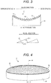
- FIG. 3 is an arrow view illustrating an A-A cross-section of the concave diffraction grating 2 illustrated in FIG. 2 and is an enlarged view of grating grooves.
- the concave diffraction grating 2 includes a concave substrate 24 having a curvature, a metal layer 22 on which a grating groove 21 is formed, and a resin layer 23 for fixing the metal layer 22 on the concave substrate 24.
- the reflective surface (surface) of the concave diffraction grating forms a portion of a spherical surface. Therefore, the concave diffraction grating may be referred to as a spherical diffraction grating.
- a concave diffraction grating having equal spacing grating grooves an image is formed on a Roland circle.
- an image can be formed approximately on a straight line.
- the concave diffraction grating 2 in which the spacing between the grating grooves 21 is gradually reduced in the blaze direction, an image can be formed approximately on a straight line.
- the blaze direction is defined as a direction from an apex angle 211 of the sawtooth grating groove 21 to an apex having the minimum angle (blaze angle 212). Therefore, such a concave diffraction grating has a shape in which the spacing between the grating grooves 21 adjacent to each other gradually changes from a wide spacing to a narrow spacing in the blaze direction.
- the concave diffraction grating 2 in which the spacing is arithmetically reduced in the blaze direction is applied to the optical device 1 illustrated in FIG. 1 , and thereby a plurality of detectors 16 can be arranged on a straight line.
- the concave diffraction grating 2 has a constant blaze angle 212, it is possible to selectively disperse light having a unique wavelength. Accordingly, it is possible to obtain the optical device 1 having low noise (stray light) and to improve detection efficiency.
- an optical device in which it is possible to improve the diffraction efficiency by suppressing the spherical aberration and to install the detector on a straight line, by mounting the concave diffraction grating including grating grooves having a sawtooth shape with a constant blaze angle and arranged at the unequal spacing on the optical device.
- FIG. 4 is a perspective view schematically illustrating a configuration of a mold of a concave diffraction grating in Embodiment 2 according to another embodiment of the present invention.
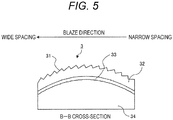
- FIG. 5 is an arrow view illustrating a B-B cross-section of the mold of the concave diffraction grating illustrated in FIG. 4 .
- a mold 3 of the concave diffraction grating is configured by a convex substrate 34 having a curvature, a metal diffraction grating 32 which is a metal film on which a grating groove 31 is formed, and an adhesive layer 33 for fixing the metal diffraction grating 32 being the metal film, on the convex substrate 34.
- the spacing between the grating grooves 31 of the metal diffraction grating 32 forming the mold 3 of the concave diffraction grating is arithmetically increased in the blaze direction.
- the spacing between the grating grooves 31 of the metal diffraction grating 32 is gradually increased in the blaze direction. Therefore, along the blaze direction, the metal diffraction grating 32 forming the mold 3 of the concave diffraction grating has a shape in which the spacing between the grating grooves 31 adjacent to each other gradually changes from a narrow spacing to a wide spacing.
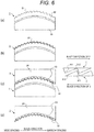
- FIG. 6 is a diagram illustrating a method for producing a concave diffraction grating using the mold of the concave diffraction grating illustrated in FIG. 4 .
- FIG. 6(a) is a diagram illustrating a step of preparing the mold of the concave diffraction grating.
- FIG. 6(b) is a diagram illustrating a step of forming a metal layer on the mold of the concave diffraction grating.
- FIG. 6(c) is a diagram illustrating a step of installing a concave substrate on the metal layer.
- FIG. 6(d) is a diagram illustrating a step of obtaining the concave diffraction grating by being separated from the mold of the concave diffraction grating.
- the mold 3 of the concave diffraction grating having the sawtooth grating grooves 31 is prepared in the step of preparing a mold of a concave diffraction grating illustrated in FIG. 6(a) .
- a separation layer (not illustrated) and the metal layer 22 are formed on the mold 3 of the concave diffraction grating having the sawtooth grating grooves 31.
- the resin layer 23 is formed on the metal layer 22, and then the concave substrate 24 is installed on the resin layer 23.
- the resin layer 23 is cured, and then the metal layer 22, the resin layer 23, and the concave substrate 24 are removed from the mold 3 of the concave diffraction grating. In this manner, the concave diffraction grating 2 is produced.
- the grating groove 31 may be transferred to the resin layer 23 by a technique such as nanoimprint using the mold 3 of the concave diffraction grating, and then the metal layer 22 may be formed on the surface thereof.
- the concave diffraction grating 2 is formed by transferring the mold 3 of the concave diffraction grating.
- a method for producing the mold of the concave diffraction grating will be described.
- a plurality of producing methods as follows can be used in the method for producing the concave diffraction grating represented by the spherical diffraction grating.
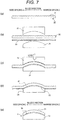
- FIG. 7 is a diagram illustrating a method for producing a mold of a concave diffraction grating in Embodiment 3 according to still another embodiment of the present invention.
- FIG. 7(a) is a diagram illustrating a step of forming a metal diffraction grating.
- FIG. 7 (b) is a diagram illustrating a step of installing a concave substrate above the metal diffraction grating and installing a convex substrate below the metal diffraction grating.
- FIG. 7(c) is a diagram illustrating a bonding step.
- FIG. 7(d) is a diagram illustrating a step of detaching the concave substrate.
- FIG. 7(e) is a diagram illustrating a step of obtaining the mold of the concave diffraction grating by removing an outer peripheral portion of the metal diffraction grating.
- the grating grooves 31 that have a sawtooth shape and have a spacing that is arithmetically increased in the blaze direction is mechanically engraved on a planar metal substrate, and thereby the metal diffraction grating 32 is formed.
- the spacing between the grating grooves 31 of the metal diffraction grating 32 is gradually increased in the blaze direction. Therefore, the metal diffraction grating 32 has a shape in which the spacing between the grating grooves 31 adjacent to each other gradually changes from the narrow spacing to the wide spacing in the blaze direction.
- the surface of the metal diffraction grating 32 on which the grating grooves 31 are formed is set as a concave substrate 35 side, and the adhesive layer 33 is installed on an opposite surface of the surface on which the grating grooves 31 are formed, that is, on a convex substrate 34 side.
- the concave substrate 35 is installed above the surface of the metal diffraction grating 32 on which the grating grooves 31 are formed, so that the concave surface of the concave substrate 35 faces the surface of the metal diffraction grating 32 on which the grating grooves 31 are formed, and the adhesive layer 33 is installed below an opposite surface of the surface of the metal diffraction grating 32 on which the grating grooves 31 are formed, so that the lower surface of the adhesive layer 33 faces the convex surface of the convex substrate 34.
- a temperature which is equal to or higher than the softening point of the adhesive layer 33 and a load are applied so that the formation surface of the grating groove 31 of the metal diffraction grating 32 is imitated on the concave substrate 35.
- the metal diffraction grating 32 is bonded to the convex surface of the convex substrate 34 by the adhesive layer 33.
- the adhesive layer 33 is cured by cooling with the load applied, and then the concave substrate 35 is detached (removed) .
- the mold 3 of the concave diffraction grating is formed by removing the outer peripheral portion of the metal diffraction grating 32 deformed on the curved surface (outer peripheral portion which is outside the convex surface of the convex substrate 34 in the metal diffraction grating 32).
- the surface on which the grating grooves 31 are formed serves as the surface accuracy of the concave substrate 35.
- the adhesive layer 33 is softened during bonding, and thus can absorb the influence of the thickness variation of the metal diffraction grating 32 and the surface accuracy variation of the convex substrate 34.
- the metal diffraction grating 32 in which the grating grooves 31 are formed on a metal planar substrate is produced by mechanical engraving or a semiconductor process (photo-lithography and etching), or the metal diffraction grating 32 is produced in a manner that a planar diffraction grating on which the grating grooves 31 are formed is transferred to a metal planar substrate by mechanical engraving or a semiconductor process. Sputtering, vapor deposition, and plating are used to transfer the grating grooves of the planar diffraction grating to the metal planar substrate.
- the mold 3 of the concave diffraction grating is produced by deforming the metal diffraction gratings 32 into the curved surface and mounting the metal diffraction gratings on the convex substrate 34.
- the mold 3 of the concave diffraction grating is transferred to the metal layer 22 and the resin layer 23 by the method illustrated in FIG. 6 in Embodiment 1 described above, and thus the concave diffraction grating 2 is produced.
- the angle of the engraving tool is constant.
- the sawtooth grating groove 31 having a constant blaze angle 312 can be formed to have small shape variation on the entire surface of the substrate.
- the sawtooth grating groove 31 having a constant blaze angle 312 ( FIG. 6 ) can be easily formed to have small shape variation, in comparison to photo-lithography and etching on a curved surface.
- a conventional device used for photo-lithography and etching can be applied.
- planar diffraction grating substrate (metal diffraction grating) 32 produced by the above method is deformed into the curved surface, and then is mounted on the convex substrate 34, it is possible to produce the mold 3 of the concave diffraction grating having grating grooves 31 in which a sawtooth shape having a substantially constant blaze angle is provided, and the spacing is arithmetically changed in the blaze direction on the entire surface of the curved surface (convex surface).
- the metal diffraction grating 32 In the deformation of the metal diffraction grating 32 into the curved surface and mounting the metal diffraction grating on the convex substrate 34, the metal diffraction grating 32 is interposed between the concave substrate 35 and the convex substrate 34 having high surface accuracy. The load and the temperature are applied to produce the mold 3 of the concave diffraction grating.
- the surface of the metal diffraction grating 32 on which the grating grooves 31 are formed is imitated to the concave substrate 35, it is possible to improve the surface accuracy of the mold 3 of the concave diffraction grating without influences of the substrate thickness variation of the metal diffraction grating 32, the thickness variation of the adhesive layer 33 for fixing the metal diffraction grating 32 and the convex substrate 34, the surface accuracy of the convex substrate, and the like.
- the metal diffraction grating 32 is interposed between the concave substrate 35 and the convex substrate 34 and is deformed into the curved surface by applying a load, there is a concern that the grating groove 31 may be deformed or crushed.
- the mold 3 of the concave diffraction grating having the grating grooves 31 that have a sawtooth shape having a substantially constant blaze angle and have a spacing that is arithmetically changed in the blaze direction, on the entire surface of the curved surface (convex surface).
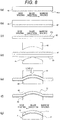
- FIG. 8 is a diagram illustrating a method for producing a mold of a concave diffraction grating in Embodiment 4 according to still yet another embodiment of the present invention.
- FIG. 8(a) is a diagram illustrating a step of forming a planar diffraction grating.
- FIG. 8(b) is a diagram illustrating a step of forming a metal diffraction grating.
- FIG. 8(c) is a diagram illustrating a step of separating the metal diffraction grating from the planar diffraction grating.
- FIG. 8(a) is a diagram illustrating a step of forming a planar diffraction grating.
- FIG. 8(b) is a diagram illustrating a step of forming a metal diffraction grating.
- FIG. 8(c) is a diagram illustrating a step of separating the metal diffraction grating from the planar diffraction grating
- FIG. 8(d) is a diagram illustrating a step of installing a concave substrate above the metal diffraction grating and installing a convex substrate below the metal diffraction grating.
- FIG. 8(e) is a diagram illustrating a bonding step.
- FIG. 8(f) is a diagram illustrating a step of detaching the concave substrate.
- FIG. 8 (g) is a diagram illustrating a step of obtaining the mold of the concave diffraction grating by removing an outer peripheral portion of the metal diffraction grating.
- grating grooves 41a having a sawtooth shape are reduced arithmetically in the blaze direction by mechanical engraving on a planar substrate to form a planar diffraction grating 40.
- the spacing between the grating grooves 41a of the planar diffraction grating 40 is gradually reduced in the blaze direction. Therefore, the planar diffraction grating 40 has a shape in which the spacing between the grating grooves 41a adjacent to each other gradually changes from the wide spacing to the narrow spacing in the blaze direction.
- a seed film is formed on the surface on which the grating grooves 41a are formed. Then, the metal is stacked by electrolytic plating to form a metal diffraction grating 42.
- the seed film is etched from the planar diffraction grating 40 to separate the metal diffraction grating 42.
- sawtooth grating grooves 41b of the metal diffraction grating 42 are formed to have a spacing that is arithmetically increased in the blaze direction.
- the spacing between the grating grooves 41b of the metal diffraction grating 42 is gradually increased in the blaze direction. Therefore, the metal diffraction grating 42 has a shape in which the spacing between the grating grooves 41b adjacent to each other gradually changes from the narrow spacing to the wide spacing in the blaze direction.
- the surface of the metal diffraction grating 42 on which the grating grooves 41b are formed is set as a concave substrate 45 side, and an adhesive layer 43 and a convex substrate 44 are installed on an opposite surface of the surface on which the grating grooves 41b are formed.
- the concave substrate 45 is installed above the surface of the metal diffraction grating 42 on which the grating grooves 41b are formed, so that the concave surface of the concave substrate 45 faces the surface of the metal diffraction grating 42 on which the grating grooves 41b are formed, and the adhesive layer 43 is installed below an opposite surface of the surface of the metal diffraction grating 42 on which the grating grooves 41b are formed, so that the lower surface of the adhesive layer 43 faces the convex surface of the convex substrate 44.
- a temperature which is equal to or higher than the softening point of the adhesive layer 43 and a load are applied so that the formation surface of the grating groove 41b of the metal diffraction grating 42 is imitated on the concave substrate 45.
- the metal diffraction grating 42 is bonded to the convex surface of the convex substrate 44 by the adhesive layer 43.
- the adhesive layer 43 is cured by cooling with the load applied, and then the concave substrate 45 is detached (removed).
- a mold 4 of the concave diffraction grating is formed by removing the outer peripheral portion of the metal diffraction grating 42 deformed on the curved surface (outer peripheral portion which is outside the convex surface of the convex substrate 44 in the metal diffraction grating 42).
- FIG. 9 is a diagram illustrating a method for producing a mold of a concave diffraction grating in Embodiment 5 according to still yet another embodiment of the present invention.
- FIG. 9(a) is a diagram illustrating a step of forming a metal diffraction grating.
- FIG. 9(b) is a diagram illustrating a step of installing a concave substrate above the metal diffraction grating and installing a convex substrate below the metal diffraction grating.
- FIG. 9(c) is a diagram illustrating a bonding step.
- FIG. 9(d) is a diagram illustrating a step of detaching the concave substrate.
- FIG. 9 (e) is a diagram illustrating a step of obtaining the mold of the concave diffraction grating by removing an outer peripheral portion of the metal diffraction grating.
- sawtooth grating grooves 51 having a spacing that is arithmetically increased in the blaze direction is formed by a semiconductor process (photo-lithography and etching) on a planar metal substrate, and thus a metal diffraction grating 52 is formed.
- the spacing between the grating grooves 51 of the metal diffraction grating 52 is gradually increased in the blaze direction. Therefore, the metal diffraction grating 52 has a shape in which the spacing between the grating grooves 51 adjacent to each other gradually changes from the narrow spacing to the wide spacing in the blaze direction.
- the surface of the metal diffraction grating 52 on which the grating grooves 51 are formed is set as a concave substrate 55 side, and an adhesive layer 53 and a convex substrate 54 are installed on an opposite surface of the surface on which the grating grooves 51 are formed.
- the concave substrate 55 is installed above the surface of the metal diffraction grating 52 on which the grating grooves 51 are formed, so that the concave surface of the concave substrate 55 faces the surface of the metal diffraction grating 52 on which the grating grooves 51 are formed, and the adhesive layer 53 is installed below an opposite surface of the surface of the metal diffraction grating 52 on which the grating grooves 51 are formed, so that the lower surface of the adhesive layer 53 faces the convex surface of the convex substrate 54.
- a temperature which is equal to or higher than the softening point of the adhesive layer 53 and a load are applied so that the formation surface of the grating groove 51 of the metal diffraction grating 52 is imitated on the concave substrate 55.
- the metal diffraction grating 52 is bonded to the convex surface of the convex substrate 54 by the adhesive layer 53.
- the adhesive layer 53 is cured by cooling with the load applied, and then the concave substrate 55 is detached (removed) .
- a mold 5 of the concave diffraction grating is formed by removing the outer peripheral portion of the metal diffraction grating 52, which is not bonded to the convex surface of the convex substrate 54 (outer peripheral portion which is outside the convex surface of the convex substrate 54 in the metal diffraction grating 52).
- the sawtooth grating grooves 51 having a spacing that is arithmetically increased in the blaze direction is formed by the semiconductor process (photo-lithography and etching) on the planar metal substrate, and thus the metal diffraction grating 52 is formed, it is possible to perform producing in a short time in comparison to producing of the metal diffraction grating 52 by mechanical engraving.
- FIG. 10 is a diagram illustrating a method for producing a mold of a concave diffraction grating in Embodiment 6 according to still yet another embodiment of the present invention.
- FIG. 10(a) is a diagram illustrating a step of forming a planar diffraction grating.
- FIG. 10(b) is a diagram illustrating a step of stacking a metal material.
- FIG. 10(c) is a diagram illustrating a step of forming a metal diffraction grating.
- FIG. 10(d) is a diagram illustrating a step of installing a concave substrate above the metal diffraction grating and installing a convex substrate below the metal diffraction grating.
- FIG. 10(a) is a diagram illustrating a step of forming a planar diffraction grating.
- FIG. 10(b) is a diagram illustrating a step of stacking a metal material.
- FIG. 10(c)
- FIG. 10(e) is a diagram illustrating a bonding step.
- FIG. 10(f) is a diagram illustrating a step of detaching the concave substrate.
- FIG. 10(g) is a diagram illustrating a step of obtaining the mold of the concave diffraction grating by removing an outer peripheral portion of the metal diffraction grating.
- grating grooves 61a having a sawtooth shape is formed on a planar substrate with a spacing that is arithmetically reduced in the blaze direction.
- a planar diffraction grating 60 is formed.
- the grating grooves 61a are formed by photo-lithography with a resist (resin).
- the spacing between the grating grooves 61a of the planar diffraction grating 60 is gradually reduced in the blaze direction. Therefore, the planar diffraction grating 60 has a shape in which the spacing between the grating grooves 61a adjacent to each other gradually changes from the wide spacing to the narrow spacing in the blaze direction.
- a seed film is formed on the surface on which the grating grooves 61a are formed, and then the metal material is stacked by electrolytic plating.
- the metal material is separated from the planar diffraction grating 60, and thus a metal diffraction grating 62 having sawtooth grating grooves 61b is formed with a spacing that is arithmetically increased in the blaze direction.
- the spacing between grating grooves 61b of the metal diffraction grating 62 is gradually increased in the blaze direction. Therefore, the metal diffraction grating 62 has a shape in which the spacing between the grating grooves 61b adjacent to each other gradually changes from the narrow spacing to the wide spacing in the blaze direction.
- planar diffraction grating 60 it is possible to produce the planar diffraction grating 60 by photo-lithography in a short time in comparison to producing with mechanical engraving.
- metal diffraction grating 62 it is possible to easily separate the metal diffraction grating 62 from the planar diffraction grating 60 by dissolving the resist (resin), when the metal diffraction grating 62 is intended to be separated from the planar diffraction grating 60.
- the surface of the metal diffraction grating 62 on which the grating grooves 61b are formed is set as a concave substrate 65 side, and an adhesive layer 63 and a convex substrate 64 are installed on an opposite surface of the surface on which the grating grooves 61b are formed.
- the concave substrate 65 is installed above the surface of the metal diffraction grating 62 on which the grating grooves 61b are formed, so that the concave surface of the concave substrate 65 faces the surface of the metal diffraction grating 62 on which the grating grooves 61b are formed, and the adhesive layer 63 is installed below an opposite surface of the surface of the metal diffraction grating 62 on which the grating grooves 61b are formed, so that the lower surface of the adhesive layer 63 faces the convex surface of the convex substrate 64.
- a temperature which is equal to or higher than the softening point of the adhesive layer 63 and a load are applied so that the formation surface of the grating groove 61b of the metal diffraction grating 62 is imitated on the concave substrate 65.
- the metal diffraction grating 62 is bonded to the convex surface of the convex substrate 64 by the adhesive layer 63.
- the adhesive layer 63 is cured by cooling with the load applied, and then the concave substrate 65 is detached (removed) .
- a mold 6 of the concave diffraction grating is formed by removing the outer peripheral portion of the metal diffraction grating 62 deformed on a curved surface, which is not bonded to the convex surface of the convex substrate 64 (outer peripheral portion which is outside the convex surface of the convex substrate 64 in the metal diffraction grating 62).
- planar diffraction grating 60 is produced by photo-lithography, it is possible to produce the planar diffraction grating 60 in a short time in comparison to producing by mechanical engraving. In addition, it is possible to easily separate the metal diffraction grating 62 from the planar diffraction grating 60 by dissolving the resist (resin), when the metal diffraction grating 62 is intended to be separated from the planar diffraction grating 60.
Landscapes
- Physics & Mathematics (AREA)
- Spectroscopy & Molecular Physics (AREA)
- General Physics & Mathematics (AREA)
- Optics & Photonics (AREA)
- Engineering & Computer Science (AREA)
- Manufacturing & Machinery (AREA)
- Health & Medical Sciences (AREA)
- Ophthalmology & Optometry (AREA)
- Mechanical Engineering (AREA)
- Diffracting Gratings Or Hologram Optical Elements (AREA)
- Spectrometry And Color Measurement (AREA)
Abstract
Description
- The present invention relates to a concave diffraction grating and a method for producing the same, and more particularly to a curved diffraction grating for dispersing and converging light and an optical device using the same.
- As the background technology in the present technical field, a curved diffraction grating being an optical element mounted on an optical device such as a spectrophotometer has both light dispersion and convergence performances. Thus, it is possible to reduce the number of components and to simplify the configuration of a device.
- Conventionally, in a spherical concave diffraction grating, if a spacing between grating grooves is equal, the spectral light is focused on the Roland circle. Thus, it is possible to improve the performance of an optical device by installing a detector on the Roland circle. However, there is a concern that the size of the optical device may be increased by installing the detector on the Roland circle. Therefore, by making a spacing between the grating grooves formed in the concave diffraction grating be unequal, it is possible to correct the focusing position, that is, the installation location of the detector from the Roland circle to an approximate linear position, and thus to reduce the size of the optical device. In order to realize such a spherical concave diffraction grating, for example, the methods disclosed in
PTLs 1 to 3 have been proposed. - Regarding a concave diffraction grating, a mold of the concave diffraction grating is produced by a method of engraving a grating groove on a convex substrate with a machine such as a ruling engine. Then, the engraved grating groove is transferred to resin, metal, and the like, and thereby producing the concave diffraction grating. In the spherical concave diffraction grating, the aberration of the spectral light is suppressed by setting the spacing between the grating grooves to be unequal, as disclosed in
PTL 1. - Further, in
PTL 2, a resist is formed on a concave substrate so that a spacing between grating grooves is unequal, and a laminar type (rectangular) grating groove is formed by ion etching to produce a concave diffraction grating. InPTL 3, a planar diffraction grating having a sawtooth grating groove is interposed between uneven surface substrates, is deformed, and is joined onto a convex surface substrate to form a mold of a concave diffraction grating. The concave diffraction grating is produced by transferring the mold of the concave diffraction grating to metal, resin, or the like. -
- PTL 1:
JP S55-13918 A - PTL 1:
JP 2011-106842 A - PTL 3:
WO 2016/059928 - In a spherical concave diffraction grating, if the spacing between grating grooves is equal, the spectral light is focused on the Roland circle. Thus, it is possible to improve the performance of an optical device by installing a detector on the Roland circle. However, there is a concern that the size of the optical device may be increased by installing the detector on the Roland circle. Therefore, by making the spacing between the grating grooves formed in the concave diffraction grating be unequal, it is possible to correct the focusing position, that is, the installation location of the detector from the Roland circle to an approximate linear position, and thus to reduce the size of the optical device. However, there are problems as follows.
- In the method for producing a concave diffraction grating, which is disclosed in
PTL 1, if a mold of a diffraction grating is produced by the method of engraving a convex substrate with a machine such as a ruling engine, the angle of the engraving tool is constant. Thus, there is a problem that a shallow portion and a deep portion are formed in a sawtooth grating groove at the center portion and the end portion of a curved substrate, and thus a blaze angle is not constant. - In the method for producing a curved diffraction grating using a semiconductor process, which is disclosed in
PTL 2, it is difficult to accurately produce a grating groove pattern of the resist on any curved substrate by photo-lithography, and etching on the curved surface may cause a problem that a laminar type (rectangular) grating groove having an inclination is formed from the perpendicular line of the curved surface. - In the technique for producing a mold of a curved diffraction grating, which is disclosed in
PTL 3, a sawtooth grating groove is formed on a planar substrate and then joined to a curved surface. Thus, it is possible to produce a concave diffraction grating having a constant blaze angle even at the center portion and the end portion of a curved substrate. However, suppression of aberrations is insufficient because the grating grooves are evenly spaced. The diffraction efficiency is lowered. Thus, it is not possible to effectively utilize detected light. - Further, if the laminar type diffraction grating disclosed in
PTL 2 is produced on a planar substrate and the method disclosed inPTL 3 is applied, it is possible to produce the curved diffraction grating that does not have an inclination in the perpendicular direction of the curved surface and has rectangular grating groove with the unequal spacing. However, the curved diffraction grating is interposed between the uneven surface substrates. Thus, if a load is applied, the load is applied to the rectangular grating groove, and the rectangular grating groove may be damaged. In addition, when the mold of the concave diffraction grating is transferred, there is a problem that it is difficult to separate the concave diffraction grating from the mold because the rectangular grating groove is engaged. - Therefore, the present invention provides a concave diffraction grating capable of improved diffraction efficiency by suppressing spherical aberration.
- Further, the present invention provides an optical device in which it is possible to improve the diffraction efficiency by suppressing the spherical aberration and to install the detector on a straight line, by mounting the concave diffraction grating including grating grooves having a sawtooth shape with a constant blaze angle and arranged at the unequal spacing on the optical device.
- In order to solve the above problems, a concave diffraction grating according to the present invention disperses and focuses light. The concave diffraction grating includes a sawtooth grating groove on a concave substrate. The spacing between the sawtooth grating grooves is unequal.
- Further, according to the present invention, a concave diffraction grating is for dispersing and focusing light. The concave diffraction grating is formed by preparing a planar diffraction grating with a sawtooth shape which is formed on a planar substrate by photo-lithography and etching or machining and which forms unequally spaced grating grooves, deforming and mounting the planar diffraction grating along a fixed convex substrate to obtain a mold of a concave diffraction grating, and transferring the mold of the concave diffraction grating to a surface of a metal or a resin.
- Further, according to the present invention, a concave diffraction grating is for dispersing and focusing light. The concave diffraction grating is formed by preparing a first planar diffraction grating substrate with a sawtooth shape which is formed on a planar substrate by photo-lithography and etching or machining and which forms unequally spaced grating grooves, deforming and mounting a second diffraction grating substrate in a planar shape onto which a diffraction grating pattern formed on the first planar diffraction grating substrate is transferred, along a fixed convex substrate to obtain a mold of a concave diffraction grating, and transferring the mold of the concave diffraction grating to a surface of a metal or a resin.
- Further, according to the present invention, an optical device includes a first focusing lens that focuses light emitted from a light source and irradiates a sample with the light, a second focusing lens that focuses transmitted light obtained by light being transmitted through the sample, to an opening portion of a slit, and a concave diffraction grating that wavelength-disperses the light that is transmitted through the opening portion of the slit and guides the light to a plurality of detectors. The concave diffraction grating has sawtooth grating grooves on a concave substrate, and a spacing between the sawtooth grating grooves is unequal.
- Further, according to the present invention, there is provided a method for producing a concave diffraction grating. The method includes (1) a step of forming a sawtooth shape on a planar substrate by photo-lithography and etching or machining to form unequal spacing grating grooves and to prepare a planar diffraction grating substrate, (2) a step of installing a concave substrate so that a concave surface faces a surface on which the grating grooves are formed and installing a convex substrate through an adhesive layer so that a convex surface faces an opposite surface of the surface on which the grating grooves are formed, (3) a bonding step of imitating the surface of the planar diffraction grating substrate, on which the grating grooves are formed, onto the concave substrate, and bonding the planar diffraction grating substrate to the convex substrate by the adhesive layer, (4) a step of detaching the concave substrate, and then removing an outer peripheral portion which is outside the convex surface of the convex substrate in the planar diffraction grating substrate, so as to form a mold of a concave diffraction grating, and (5) a step of transferring the mold of the concave diffraction grating to a surface of metal or resin.
- According to the present invention, it is possible to provide a concave diffraction grating capable of improving diffraction efficiency by suppressing spherical aberration.
- In addition, according to the present invention, it is possible to provide an optical device in which it is possible to improve the diffraction efficiency by suppressing the spherical aberration and to install the detector on a straight line, by mounting the concave diffraction grating including grating grooves having a sawtooth shape with a constant blaze angle and arranged at the unequal spacing on the optical device.
- Objects, configurations, and advantageous effects other than those described above will be clarified by the descriptions of the following embodiments.
-
- [
FIG. 1] FIG. 1 is an overall schematic block diagram illustrating an optical device using a concave diffraction grating inEmbodiment 1 according to an embodiment of the present invention. - [
FIG. 2] FIG. 2 is a perspective view schematically illustrating a configuration of the concave diffraction grating (spherical diffraction grating) illustrated inFIG. 1 . - [
FIG. 3] FIG. 3 is an arrow view illustrating an A-A cross-section of the concave diffraction grating illustrated inFIG. 2 and is an enlarged view of grating grooves. - [
FIG. 4] FIG. 4 is a perspective view schematically illustrating a configuration of a mold of a concave diffraction grating (spherical diffraction grating) inEmbodiment 2 according to another embodiment of the present invention. - [
FIG. 5] FIG. 5 is an arrow view illustrating a B-B cross-section of the mold of the concave diffraction grating illustrated inFIG. 4 . - [
FIG. 6] FIG. 6 is a diagram illustrating a method for producing a concave diffraction grating using the mold of the concave diffraction grating illustrated inFIG. 4 :FIG. 6(a) is a diagram illustrating a step of preparing the mold of the concave diffraction grating;FIG. 6(b) is a diagram illustrating a step of forming a metal layer on the mold of the concave diffraction grating;FIG. 6(c) is a diagram illustrating a step of installing a concave substrate on the metal layer; andFIG. 6(d) is a diagram illustrating a step of obtaining the concave diffraction grating by being separated from the mold of the concave diffraction grating. - [
FIG. 7] FIG. 7 is a diagram illustrating a method for producing a mold of a concave diffraction grating inEmbodiment 3 according to still another embodiment of the present invention:FIG. 7 (a) is a diagram illustrating a step of forming a metal diffraction grating;FIG. 7(b) is a diagram illustrating a step of installing a concave substrate above the metal diffraction grating and installing a convex substrate below the metal diffraction grating;FIG. 7 (c) is a diagram illustrating a bonding step;FIG. 7(d) is a diagram illustrating a step of detaching the concave substrate; andFIG. 7(e) is a diagram illustrating a step of obtaining the mold of the concave diffraction grating by removing an outer peripheral portion of the metal diffraction grating. - [
FIG. 8] FIG. 8 is a diagram illustrating a method for producing a mold of a concave diffraction grating inEmbodiment 4 according to still yet another embodiment of the present invention:FIG. 8 (a) is a diagram illustrating a step of forming a planar diffraction grating;FIG. 8(b) is a diagram illustrating a step of forming a metal diffraction grating;FIG. 8(c) is a diagram illustrating a step of separating the metal diffraction grating from the planar diffraction grating;FIG. 8(d) is a diagram illustrating a step of installing a concave substrate above the metal diffraction grating and installing a convex substrate below the metal diffraction grating;FIG. 8(e) is a diagram illustrating a bonding step;FIG. 8(f) is a diagram illustrating a step of detaching the concave substrate; andFIG. 8 (g) is a diagram illustrating a step of obtaining the mold of the concave diffraction grating by removing an outer peripheral portion of the metal diffraction grating. - [
FIG. 9] FIG. 9 is a diagram illustrating a method for producing a mold of a concave diffraction grating inEmbodiment 5 according to still yet another embodiment of the present invention:FIG. 9 (a) is a diagram illustrating a step of forming a metal diffraction grating;FIG. 9 (b) is a diagram illustrating a step of installing a concave substrate above the metal diffraction grating and installing a convex substrate below the metal diffraction grating;FIG. 9 (c) is a diagram illustrating a bonding step;FIG. 9(d) is a diagram illustrating a step of detaching the concave substrate; andFIG. 9(e) is a diagram illustrating a step of obtaining the mold of the concave diffraction grating by removing an outer peripheral portion of the metal diffraction grating. - [
FIG. 10] FIG. 10 is a diagram illustrating a method for producing a mold of a concave diffraction grating in Embodiment 6 according to still yet another embodiment of the present invention:FIG. 10(a) is a diagram illustrating a step of forming a planar diffraction grating;FIG. 10(b) is a diagram illustrating a step of stacking a metal material;FIG. 10(c) is a diagram illustrating a step of forming a metal diffraction grating;FIG. 10(d) is a diagram illustrating a step of installing a concave substrate above the metal diffraction grating and installing a convex substrate below the metal diffraction grating;FIG. 10(e) is a diagram illustrating a bonding step;FIG. 10(f) is a diagram illustrating a step of detaching the concave substrate; andFIG. 10(g) is a diagram illustrating a step of obtaining the mold of the concave diffraction grating by removing an outer peripheral portion of the metal diffraction grating. - Hereinafter, embodiments of the present invention will be described with reference to the drawings.
-
FIG. 1 is an overall schematic block diagram illustrating an optical device using a concave diffraction grating inEmbodiment 1 according to an embodiment of the present invention. Anoptical device 1 selectively absorbs light having a wavelength unique to a chemical bond of a chemical substance, a biological substance, or the like, and is used for concentration measurement and substance identification. As illustrated inFIG. 1 , theoptical device 1 includes awhite light source 11, a focusinglens 12a, asample chamber 13, a focusinglens 12b, aslit 14, aconcave diffraction grating 2, anddetectors 16 arranged on a plurality of straight lines. - Light from the
white light source 11 is focused by the focusinglens 12a, and a measurement target in thesample chamber 13 is irradiated with the focused light. Light transmitted through thesample chamber 13 is focused on an opening portion of theslit 14 by the focusinglens 12b. Light that has passed through theslit 14 is wavelength-dispersed by theconcave diffraction grating 2 to form a spectrum. Thedetector 16 detects the formed spectrum. - The
concave diffraction grating 2 will be described.FIG. 2 is a perspective view schematically illustrating a configuration of theconcave diffraction grating 2 illustrated inFIG. 1 .FIG. 3 is an arrow view illustrating an A-A cross-section of theconcave diffraction grating 2 illustrated inFIG. 2 and is an enlarged view of grating grooves. As illustrated inFIGS. 2 and3 , theconcave diffraction grating 2 includes aconcave substrate 24 having a curvature, ametal layer 22 on which agrating groove 21 is formed, and aresin layer 23 for fixing themetal layer 22 on theconcave substrate 24. The reflective surface (surface) of the concave diffraction grating forms a portion of a spherical surface. Therefore, the concave diffraction grating may be referred to as a spherical diffraction grating. In a concave diffraction grating having equal spacing grating grooves, an image is formed on a Roland circle. On the other hand, as illustrated inFIG. 3 , in theconcave diffraction grating 2 in which the spacing between thegrating grooves 21 is arithmetically reduced in a blaze direction, an image can be formed approximately on a straight line. In other words, in theconcave diffraction grating 2 in which the spacing between thegrating grooves 21 is gradually reduced in the blaze direction, an image can be formed approximately on a straight line. Here, as illustrated inFIG. 3 , the blaze direction is defined as a direction from anapex angle 211 of thesawtooth grating groove 21 to an apex having the minimum angle (blaze angle 212). Therefore, such a concave diffraction grating has a shape in which the spacing between thegrating grooves 21 adjacent to each other gradually changes from a wide spacing to a narrow spacing in the blaze direction. - As described above, the
concave diffraction grating 2 in which the spacing is arithmetically reduced in the blaze direction is applied to theoptical device 1 illustrated inFIG. 1 , and thereby a plurality ofdetectors 16 can be arranged on a straight line. Thus, it is possible to simplify mounting of thedetectors 16 and to reduce the size of theoptical device 1. - Further, since the
concave diffraction grating 2 has aconstant blaze angle 212, it is possible to selectively disperse light having a unique wavelength. Accordingly, it is possible to obtain theoptical device 1 having low noise (stray light) and to improve detection efficiency. - As described above, according to the present embodiment, it is possible to provide a concave diffraction grating capable of improving diffraction efficiency by suppressing spherical aberration.
- In addition, according to the present embodiment, it is possible to provide an optical device in which it is possible to improve the diffraction efficiency by suppressing the spherical aberration and to install the detector on a straight line, by mounting the concave diffraction grating including grating grooves having a sawtooth shape with a constant blaze angle and arranged at the unequal spacing on the optical device.
- In addition, according to the present embodiment, since it is possible to install the detectors on a straight line, it is possible to realize a small optical device.
- Further, it is possible to realize a low-cost optical device having a small number of optical element components.
- A structure of a mold of the concave diffraction grating and a method for producing the concave diffraction grating will be described with reference to
FIGS. 4 to 6 .FIG. 4 is a perspective view schematically illustrating a configuration of a mold of a concave diffraction grating inEmbodiment 2 according to another embodiment of the present invention.FIG. 5 is an arrow view illustrating a B-B cross-section of the mold of the concave diffraction grating illustrated inFIG. 4 . - As illustrated in
FIGS. 4 and5 , amold 3 of the concave diffraction grating is configured by aconvex substrate 34 having a curvature, ametal diffraction grating 32 which is a metal film on which agrating groove 31 is formed, and anadhesive layer 33 for fixing themetal diffraction grating 32 being the metal film, on theconvex substrate 34. As illustrated inFIG. 5 , the spacing between thegrating grooves 31 of themetal diffraction grating 32 forming themold 3 of the concave diffraction grating is arithmetically increased in the blaze direction. In other words, the spacing between thegrating grooves 31 of themetal diffraction grating 32 is gradually increased in the blaze direction. Therefore, along the blaze direction, themetal diffraction grating 32 forming themold 3 of the concave diffraction grating has a shape in which the spacing between thegrating grooves 31 adjacent to each other gradually changes from a narrow spacing to a wide spacing. - Next, a direction of producing the
concave diffraction grating 2 described inEmbodiment 1 described above will be described.FIG. 6 is a diagram illustrating a method for producing a concave diffraction grating using the mold of the concave diffraction grating illustrated inFIG. 4 .FIG. 6(a) is a diagram illustrating a step of preparing the mold of the concave diffraction grating.FIG. 6(b) is a diagram illustrating a step of forming a metal layer on the mold of the concave diffraction grating.FIG. 6(c) is a diagram illustrating a step of installing a concave substrate on the metal layer.FIG. 6(d) is a diagram illustrating a step of obtaining the concave diffraction grating by being separated from the mold of the concave diffraction grating. - Firstly, the
mold 3 of the concave diffraction grating having thesawtooth grating grooves 31 is prepared in the step of preparing a mold of a concave diffraction grating illustrated inFIG. 6(a) . - Then, in the step of forming a metal layer on the mold of the concave diffraction grating illustrated in
FIG. 6(b) , a separation layer (not illustrated) and themetal layer 22 are formed on themold 3 of the concave diffraction grating having thesawtooth grating grooves 31. In the step of installing a concave substrate on the metal layer illustrated inFIG. 6(c) , theresin layer 23 is formed on themetal layer 22, and then theconcave substrate 24 is installed on theresin layer 23. - In the step of obtaining the concave diffraction grating by being separated from the mold of the concave diffraction grating illustrated in
FIG. 6(d) , theresin layer 23 is cured, and then themetal layer 22, theresin layer 23, and theconcave substrate 24 are removed from themold 3 of the concave diffraction grating. In this manner, theconcave diffraction grating 2 is produced. - Note that, the grating
groove 31 may be transferred to theresin layer 23 by a technique such as nanoimprint using themold 3 of the concave diffraction grating, and then themetal layer 22 may be formed on the surface thereof. Here, theconcave diffraction grating 2 is formed by transferring themold 3 of the concave diffraction grating. Thus, as illustrated in the right figure ofFIG. 6 , in order to form theconcave diffraction grating 2 in which the spacing between thegrating grooves 21 is arithmetically reduced from theapex angle 211 toward the apex having theblaze angle 212, that is, in the blaze direction (blaze direction of the concave diffraction grating 2), it is necessary to form the concave diffraction grating by arithmetically increasing the spacing between thegrating grooves 31 of themold 3 of the concave diffraction grating, from anapex angle 311 toward an apex having ablaze angle 312, that is, in the blaze direction (blaze direction of themold 3 of the concave diffraction grating). - As described above, according to the present embodiment, it is possible to easily produce the
concave diffraction grating 2 described inEmbodiment 1 described above. - Next, a method for producing the mold of the concave diffraction grating will be described. A plurality of producing methods as follows can be used in the method for producing the concave diffraction grating represented by the spherical diffraction grating.
-
FIG. 7 is a diagram illustrating a method for producing a mold of a concave diffraction grating inEmbodiment 3 according to still another embodiment of the present invention.FIG. 7(a) is a diagram illustrating a step of forming a metal diffraction grating.FIG. 7 (b) is a diagram illustrating a step of installing a concave substrate above the metal diffraction grating and installing a convex substrate below the metal diffraction grating.FIG. 7(c) is a diagram illustrating a bonding step.FIG. 7(d) is a diagram illustrating a step of detaching the concave substrate.FIG. 7(e) is a diagram illustrating a step of obtaining the mold of the concave diffraction grating by removing an outer peripheral portion of the metal diffraction grating. - In the process of forming a metal diffraction grating illustrated in
FIG. 7(a) , thegrating grooves 31 that have a sawtooth shape and have a spacing that is arithmetically increased in the blaze direction is mechanically engraved on a planar metal substrate, and thereby themetal diffraction grating 32 is formed. In other words, the spacing between thegrating grooves 31 of themetal diffraction grating 32 is gradually increased in the blaze direction. Therefore, themetal diffraction grating 32 has a shape in which the spacing between thegrating grooves 31 adjacent to each other gradually changes from the narrow spacing to the wide spacing in the blaze direction. - Then, in the step of installing a concave substrate above the metal diffraction grating and installing a convex substrate below the metal diffraction grating, illustrated in
FIG. 7(b) , the surface of themetal diffraction grating 32 on which thegrating grooves 31 are formed is set as aconcave substrate 35 side, and theadhesive layer 33 is installed on an opposite surface of the surface on which thegrating grooves 31 are formed, that is, on aconvex substrate 34 side. That is, theconcave substrate 35 is installed above the surface of themetal diffraction grating 32 on which thegrating grooves 31 are formed, so that the concave surface of theconcave substrate 35 faces the surface of themetal diffraction grating 32 on which thegrating grooves 31 are formed, and theadhesive layer 33 is installed below an opposite surface of the surface of themetal diffraction grating 32 on which thegrating grooves 31 are formed, so that the lower surface of theadhesive layer 33 faces the convex surface of theconvex substrate 34. - In the bonding step illustrated in
FIG. 7 (c) , in a vacuum atmosphere, a temperature which is equal to or higher than the softening point of theadhesive layer 33 and a load are applied so that the formation surface of thegrating groove 31 of themetal diffraction grating 32 is imitated on theconcave substrate 35. In addition, themetal diffraction grating 32 is bonded to the convex surface of theconvex substrate 34 by theadhesive layer 33. - Then, in the step of detaching the concave substrate illustrated in
FIG. 7(d) , theadhesive layer 33 is cured by cooling with the load applied, and then theconcave substrate 35 is detached (removed) . Subsequently, in the step of obtaining the mold of the concave diffraction grating by removing the outer peripheral portion of the metal diffraction grating illustrated inFIG. 7(e) , themold 3 of the concave diffraction grating is formed by removing the outer peripheral portion of themetal diffraction grating 32 deformed on the curved surface (outer peripheral portion which is outside the convex surface of theconvex substrate 34 in the metal diffraction grating 32). - Since the
metal diffraction grating 32 is deformed into the curved surface by imitating theconcave substrate 35, the surface on which thegrating grooves 31 are formed serves as the surface accuracy of theconcave substrate 35. Further, theadhesive layer 33 is softened during bonding, and thus can absorb the influence of the thickness variation of themetal diffraction grating 32 and the surface accuracy variation of theconvex substrate 34. - The
metal diffraction grating 32 in which thegrating grooves 31 are formed on a metal planar substrate is produced by mechanical engraving or a semiconductor process (photo-lithography and etching), or themetal diffraction grating 32 is produced in a manner that a planar diffraction grating on which thegrating grooves 31 are formed is transferred to a metal planar substrate by mechanical engraving or a semiconductor process. Sputtering, vapor deposition, and plating are used to transfer the grating grooves of the planar diffraction grating to the metal planar substrate. Themold 3 of the concave diffraction grating is produced by deforming themetal diffraction gratings 32 into the curved surface and mounting the metal diffraction gratings on theconvex substrate 34. - The
mold 3 of the concave diffraction grating is transferred to themetal layer 22 and theresin layer 23 by the method illustrated inFIG. 6 inEmbodiment 1 described above, and thus theconcave diffraction grating 2 is produced. - When the
grating grooves 31 are formed on a planar substrate by mechanical engraving, the angle of the engraving tool is constant. Thus, thesawtooth grating groove 31 having aconstant blaze angle 312 can be formed to have small shape variation on the entire surface of the substrate. - When the
grating grooves 31 are formed on a planar substrate by a semiconductor process, thesawtooth grating groove 31 having a constant blaze angle 312 (FIG. 6 ) can be easily formed to have small shape variation, in comparison to photo-lithography and etching on a curved surface. In addition, a conventional device used for photo-lithography and etching can be applied. Since the planar diffraction grating substrate (metal diffraction grating) 32 produced by the above method is deformed into the curved surface, and then is mounted on theconvex substrate 34, it is possible to produce themold 3 of the concave diffraction grating havinggrating grooves 31 in which a sawtooth shape having a substantially constant blaze angle is provided, and the spacing is arithmetically changed in the blaze direction on the entire surface of the curved surface (convex surface). - In the deformation of the
metal diffraction grating 32 into the curved surface and mounting the metal diffraction grating on theconvex substrate 34, themetal diffraction grating 32 is interposed between theconcave substrate 35 and theconvex substrate 34 having high surface accuracy. The load and the temperature are applied to produce themold 3 of the concave diffraction grating. Since the surface of themetal diffraction grating 32 on which thegrating grooves 31 are formed is imitated to theconcave substrate 35, it is possible to improve the surface accuracy of themold 3 of the concave diffraction grating without influences of the substrate thickness variation of themetal diffraction grating 32, the thickness variation of theadhesive layer 33 for fixing themetal diffraction grating 32 and theconvex substrate 34, the surface accuracy of the convex substrate, and the like. When themetal diffraction grating 32 is interposed between theconcave substrate 35 and theconvex substrate 34 and is deformed into the curved surface by applying a load, there is a concern that thegrating groove 31 may be deformed or crushed. Since the load applied to thegrating grooves 31 from theconcave substrate 35 is distributed in a direction adjacent to the apex angle 311 (FIG. 6 ) of thesawtooth grating grooves 31, it is possible to produce themold 3 of the concave diffraction grating without deformation or crushing. - As described above, according to the present embodiment, it is possible to produce the
mold 3 of the concave diffraction grating having thegrating grooves 31 that have a sawtooth shape having a substantially constant blaze angle and have a spacing that is arithmetically changed in the blaze direction, on the entire surface of the curved surface (convex surface). - As a result, it is possible to produce the
concave diffraction grating 2 having a sawtooth shape having a substantially constant blaze angle transferred. - Further, according to the present embodiment, it is possible to improve the surface accuracy of the
mold 3 of the concave diffraction grating. -
FIG. 8 is a diagram illustrating a method for producing a mold of a concave diffraction grating inEmbodiment 4 according to still yet another embodiment of the present invention.FIG. 8(a) is a diagram illustrating a step of forming a planar diffraction grating.FIG. 8(b) is a diagram illustrating a step of forming a metal diffraction grating.FIG. 8(c) is a diagram illustrating a step of separating the metal diffraction grating from the planar diffraction grating.FIG. 8(d) is a diagram illustrating a step of installing a concave substrate above the metal diffraction grating and installing a convex substrate below the metal diffraction grating.FIG. 8(e) is a diagram illustrating a bonding step.FIG. 8(f) is a diagram illustrating a step of detaching the concave substrate.FIG. 8 (g) is a diagram illustrating a step of obtaining the mold of the concave diffraction grating by removing an outer peripheral portion of the metal diffraction grating. - In the step of forming the planar diffraction grating illustrated in
FIG. 8 (a) , gratinggrooves 41a having a sawtooth shape are reduced arithmetically in the blaze direction by mechanical engraving on a planar substrate to form aplanar diffraction grating 40. In other words, the spacing between thegrating grooves 41a of theplanar diffraction grating 40 is gradually reduced in the blaze direction. Therefore, theplanar diffraction grating 40 has a shape in which the spacing between thegrating grooves 41a adjacent to each other gradually changes from the wide spacing to the narrow spacing in the blaze direction. - Then, in the step of forming the metal diffraction grating illustrated in
FIG. 8(b) , a seed film is formed on the surface on which thegrating grooves 41a are formed. Then, the metal is stacked by electrolytic plating to form ametal diffraction grating 42. - In the step of separating the metal diffraction grating from the planar diffraction grating illustrated in
FIG. 8(c) , the seed film is etched from theplanar diffraction grating 40 to separate themetal diffraction grating 42. Here, sawtooth gratinggrooves 41b of themetal diffraction grating 42 are formed to have a spacing that is arithmetically increased in the blaze direction. In other words, the spacing between thegrating grooves 41b of themetal diffraction grating 42 is gradually increased in the blaze direction. Therefore, themetal diffraction grating 42 has a shape in which the spacing between thegrating grooves 41b adjacent to each other gradually changes from the narrow spacing to the wide spacing in the blaze direction. - Then, in the step of installing a concave substrate above the metal diffraction grating and installing a convex substrate below the metal diffraction grating, illustrated in
FIG. 8(d) , the surface of themetal diffraction grating 42 on which thegrating grooves 41b are formed is set as aconcave substrate 45 side, and anadhesive layer 43 and aconvex substrate 44 are installed on an opposite surface of the surface on which thegrating grooves 41b are formed. That is, theconcave substrate 45 is installed above the surface of themetal diffraction grating 42 on which thegrating grooves 41b are formed, so that the concave surface of theconcave substrate 45 faces the surface of themetal diffraction grating 42 on which thegrating grooves 41b are formed, and theadhesive layer 43 is installed below an opposite surface of the surface of themetal diffraction grating 42 on which thegrating grooves 41b are formed, so that the lower surface of theadhesive layer 43 faces the convex surface of theconvex substrate 44. - In the bonding step illustrated in
FIG. 8(e) , in a vacuum atmosphere, a temperature which is equal to or higher than the softening point of theadhesive layer 43 and a load are applied so that the formation surface of thegrating groove 41b of themetal diffraction grating 42 is imitated on theconcave substrate 45. In addition, themetal diffraction grating 42 is bonded to the convex surface of theconvex substrate 44 by theadhesive layer 43. - Then, in the step of detaching the concave substrate illustrated in
FIG. 8(f) , theadhesive layer 43 is cured by cooling with the load applied, and then theconcave substrate 45 is detached (removed). Subsequently, in the step of obtaining the mold of the concave diffraction grating by removing the outer peripheral portion of the metal diffraction grating illustrated inFIG. 8(g) , amold 4 of the concave diffraction grating is formed by removing the outer peripheral portion of themetal diffraction grating 42 deformed on the curved surface (outer peripheral portion which is outside the convex surface of theconvex substrate 44 in the metal diffraction grating 42). With the above method, it is possible to form themold 4 of the concave diffraction grating having a spacing that is arithmetically increased in the blaze direction. -
FIG. 9 is a diagram illustrating a method for producing a mold of a concave diffraction grating inEmbodiment 5 according to still yet another embodiment of the present invention.FIG. 9(a) is a diagram illustrating a step of forming a metal diffraction grating.FIG. 9(b) is a diagram illustrating a step of installing a concave substrate above the metal diffraction grating and installing a convex substrate below the metal diffraction grating.FIG. 9(c) is a diagram illustrating a bonding step.FIG. 9(d) is a diagram illustrating a step of detaching the concave substrate.FIG. 9 (e) is a diagram illustrating a step of obtaining the mold of the concave diffraction grating by removing an outer peripheral portion of the metal diffraction grating. - In the process of forming the metal diffraction grating illustrated in
FIG. 9(a) ,sawtooth grating grooves 51 having a spacing that is arithmetically increased in the blaze direction is formed by a semiconductor process (photo-lithography and etching) on a planar metal substrate, and thus ametal diffraction grating 52 is formed. In other words, the spacing between thegrating grooves 51 of themetal diffraction grating 52 is gradually increased in the blaze direction. Therefore, themetal diffraction grating 52 has a shape in which the spacing between thegrating grooves 51 adjacent to each other gradually changes from the narrow spacing to the wide spacing in the blaze direction. Here, it is possible to perform producing in a short time by applying the semiconductor process (photo-lithography and etching), in comparison to producing of themetal diffraction grating 52 by mechanical engraving. - Then, in the step of installing a concave substrate above the metal diffraction grating and installing a convex substrate below the metal diffraction grating, illustrated in
FIG. 9(b) , the surface of themetal diffraction grating 52 on which thegrating grooves 51 are formed is set as aconcave substrate 55 side, and anadhesive layer 53 and aconvex substrate 54 are installed on an opposite surface of the surface on which thegrating grooves 51 are formed. That is, theconcave substrate 55 is installed above the surface of themetal diffraction grating 52 on which thegrating grooves 51 are formed, so that the concave surface of theconcave substrate 55 faces the surface of themetal diffraction grating 52 on which thegrating grooves 51 are formed, and theadhesive layer 53 is installed below an opposite surface of the surface of themetal diffraction grating 52 on which thegrating grooves 51 are formed, so that the lower surface of theadhesive layer 53 faces the convex surface of theconvex substrate 54. - In the bonding step illustrated in
FIG. 9 (c) , in a vacuum atmosphere, a temperature which is equal to or higher than the softening point of theadhesive layer 53 and a load are applied so that the formation surface of thegrating groove 51 of themetal diffraction grating 52 is imitated on theconcave substrate 55. In addition, themetal diffraction grating 52 is bonded to the convex surface of theconvex substrate 54 by theadhesive layer 53. - Then, in the step of detaching the concave substrate illustrated in
FIG. 9(d) , theadhesive layer 53 is cured by cooling with the load applied, and then theconcave substrate 55 is detached (removed) . Subsequently, in the step of obtaining the mold of the concave diffraction grating by removing the outer peripheral portion of the metal diffraction grating illustrated inFIG. 9(e) , amold 5 of the concave diffraction grating is formed by removing the outer peripheral portion of themetal diffraction grating 52, which is not bonded to the convex surface of the convex substrate 54 (outer peripheral portion which is outside the convex surface of theconvex substrate 54 in the metal diffraction grating 52). - As described above, according to the present embodiment, since the
sawtooth grating grooves 51 having a spacing that is arithmetically increased in the blaze direction is formed by the semiconductor process (photo-lithography and etching) on the planar metal substrate, and thus themetal diffraction grating 52 is formed, it is possible to perform producing in a short time in comparison to producing of themetal diffraction grating 52 by mechanical engraving. -
FIG. 10 is a diagram illustrating a method for producing a mold of a concave diffraction grating in Embodiment 6 according to still yet another embodiment of the present invention.FIG. 10(a) is a diagram illustrating a step of forming a planar diffraction grating.FIG. 10(b) is a diagram illustrating a step of stacking a metal material.FIG. 10(c) is a diagram illustrating a step of forming a metal diffraction grating.FIG. 10(d) is a diagram illustrating a step of installing a concave substrate above the metal diffraction grating and installing a convex substrate below the metal diffraction grating.FIG. 10(e) is a diagram illustrating a bonding step.FIG. 10(f) is a diagram illustrating a step of detaching the concave substrate.FIG. 10(g) is a diagram illustrating a step of obtaining the mold of the concave diffraction grating by removing an outer peripheral portion of the metal diffraction grating. - In the process of forming the planar diffraction grating illustrated in
FIG. 10 (a) , gratinggrooves 61a having a sawtooth shape is formed on a planar substrate with a spacing that is arithmetically reduced in the blaze direction. Thus, aplanar diffraction grating 60 is formed. At this time, thegrating grooves 61a are formed by photo-lithography with a resist (resin). In other words, the spacing between thegrating grooves 61a of theplanar diffraction grating 60 is gradually reduced in the blaze direction. Therefore, theplanar diffraction grating 60 has a shape in which the spacing between thegrating grooves 61a adjacent to each other gradually changes from the wide spacing to the narrow spacing in the blaze direction. - Then, in the step of stacking a metal material illustrated in
FIG. 10(b) , a seed film is formed on the surface on which thegrating grooves 61a are formed, and then the metal material is stacked by electrolytic plating. - In the step of forming the metal diffraction grating illustrated in
FIG. 10(c) , the metal material is separated from theplanar diffraction grating 60, and thus ametal diffraction grating 62 havingsawtooth grating grooves 61b is formed with a spacing that is arithmetically increased in the blaze direction. In other words, the spacing betweengrating grooves 61b of themetal diffraction grating 62 is gradually increased in the blaze direction. Therefore, themetal diffraction grating 62 has a shape in which the spacing between thegrating grooves 61b adjacent to each other gradually changes from the narrow spacing to the wide spacing in the blaze direction. Here, it is possible to produce theplanar diffraction grating 60 by photo-lithography in a short time in comparison to producing with mechanical engraving. In addition, it is possible to easily separate themetal diffraction grating 62 from theplanar diffraction grating 60 by dissolving the resist (resin), when themetal diffraction grating 62 is intended to be separated from theplanar diffraction grating 60. - Then, in the step of installing a concave substrate above the metal diffraction grating and installing a convex substrate below the metal diffraction grating, illustrated in
FIG. 10(d) , the surface of themetal diffraction grating 62 on which thegrating grooves 61b are formed is set as aconcave substrate 65 side, and anadhesive layer 63 and aconvex substrate 64 are installed on an opposite surface of the surface on which thegrating grooves 61b are formed. That is, theconcave substrate 65 is installed above the surface of themetal diffraction grating 62 on which thegrating grooves 61b are formed, so that the concave surface of theconcave substrate 65 faces the surface of themetal diffraction grating 62 on which thegrating grooves 61b are formed, and theadhesive layer 63 is installed below an opposite surface of the surface of themetal diffraction grating 62 on which thegrating grooves 61b are formed, so that the lower surface of theadhesive layer 63 faces the convex surface of theconvex substrate 64. - In the bonding step illustrated in
FIG. 10 (e) , in a vacuum atmosphere, a temperature which is equal to or higher than the softening point of theadhesive layer 63 and a load are applied so that the formation surface of thegrating groove 61b of themetal diffraction grating 62 is imitated on theconcave substrate 65. In addition, themetal diffraction grating 62 is bonded to the convex surface of theconvex substrate 64 by theadhesive layer 63. - Then, in the step of detaching the concave substrate illustrated in
FIG. 10(f) , theadhesive layer 63 is cured by cooling with the load applied, and then theconcave substrate 65 is detached (removed) . Subsequently, in the step of obtaining the mold of the concave diffraction grating by removing the outer peripheral portion of the metal diffraction grating illustrated inFIG. 10(g) , a mold 6 of the concave diffraction grating is formed by removing the outer peripheral portion of themetal diffraction grating 62 deformed on a curved surface, which is not bonded to the convex surface of the convex substrate 64 (outer peripheral portion which is outside the convex surface of theconvex substrate 64 in the metal diffraction grating 62). - As described above, according to the present embodiment, since the
planar diffraction grating 60 is produced by photo-lithography, it is possible to produce theplanar diffraction grating 60 in a short time in comparison to producing by mechanical engraving. In addition, it is possible to easily separate themetal diffraction grating 62 from theplanar diffraction grating 60 by dissolving the resist (resin), when themetal diffraction grating 62 is intended to be separated from theplanar diffraction grating 60. - The present invention is not limited to the above embodiments, and various modifications may be provided.
- For example, the above embodiments are described in detail in order to explain the present invention in an easy-to-understand manner, and the above embodiments are not necessarily limited to a case including all the described configurations. Further, some components in one embodiment can be replaced with the components in another embodiment, and the configuration of another embodiment can be added to the configuration of one embodiment.
-
- 1
- optical device
- 2
- concave diffraction grating
- 3, 4, 5, 6
- mold of concave diffraction grating
- 11
- light source
- 12a, 12b
- focusing lens
- 13
- sample chamber
- 14
- slit
- 16
- detector
- 21
- grating groove
- 22
- metal layer
- 23
- resin layer
- 24
- concave substrate
- 30, 50, 60
- planar diffraction grating
- 31, 41, 51, 61
- grating groove
- 32, 42, 52, 62
- metal diffraction grating
- 33, 43, 53, 63
- adhesive layer
- 34, 44, 54, 64
- convex substrate
- 35, 45, 55, 65
- concave substrate
Claims (17)
- A concave diffraction grating for dispersing and focusing light, the grating comprising:sawtooth grating grooves on a concave substrate,wherein the sawtooth grating grooves are unequally spaced.
- A concave diffraction grating for dispersing and focusing light, the concave diffraction grating being formed by preparing a planar diffraction grating with a sawtooth shape which is formed on a planar substrate by photo-lithography and etching or machining and which forms unequally spaced grating grooves, deforming and mounting the planar diffraction grating along a fixed convex substrate to obtain a mold of a concave diffraction grating, and transferring the mold of the concave diffraction grating to a surface of a metal or a resin.
- The concave diffraction grating according to claim 1 or 2, wherein a spacing between the grating grooves has a shape of being arithmetically reduced in a blaze direction.
- The concave diffraction grating according to claim 1 or 2, wherein a spacing between grating grooves adjacent to each other has a shape of gradually changing from a wide spacing to a narrow spacing in a blaze direction.
- The concave diffraction grating according to claim 3, wherein a concave surface for dispersing and focusing the light is a spherical surface.
- The concave diffraction grating according to claim 4, wherein a concave surface for dispersing and focusing the light is a spherical surface.
- A concave diffraction grating for dispersing and focusing light, the concave diffraction grating being formed by preparing a first planar diffraction grating substrate with a sawtooth shape which is formed on a planar substrate by photo-lithography and etching or machining and which forms unequally spaced grating grooves, deforming and mounting a second diffraction grating substrate in a planar shape onto which a diffraction grating pattern formed on the first planar diffraction grating substrate is transferred, along a fixed convex substrate to obtain a mold of a concave diffraction grating, and transferring the mold of the concave diffraction grating to a surface of a metal or a resin.
- The concave diffraction grating according to claim 7, wherein a spacing between the grating grooves has a shape of being arithmetically reduced in a blaze direction.
- The concave diffraction grating according to claim 7, wherein a spacing between grating grooves adj acent to each other has a shape of gradually changing from a wide spacing to a narrow spacing in a blaze direction.
- The concave diffraction grating according to claim 8 or 9, wherein a concave surface for dispersing and focusing the light is a spherical surface.
- An optical device comprising:a first focusing lens that focuses light emitted from a light source and irradiates a sample with the light;a second focusing lens that focuses transmitted light obtained by light being transmitted through the sample, to an opening portion of a slit; anda concave diffraction grating that wavelength-disperses the light that is transmitted through the opening portion of the slit and guides the light to a plurality of detectors,wherein the concave diffraction grating has sawtooth grating grooves on a concave substrate, anda spacing between the sawtooth grating grooves is unequal.
- The optical device according to claim 11, wherein a spacing between the grating grooves has a shape of being arithmetically reduced in a blaze direction.
- The optical device according to claim 11, wherein a spacing between grating grooves adjacent to each other has a shape of gradually changing from a wide spacing to a narrow spacing in a blaze direction.
- The optical device according to claim 12 or 13, wherein the plurality of detectors are arranged on a straight line.
- A method for producing a concave diffraction grating, the method comprising:a step of forming a sawtooth shape on a planar substrate by photo-lithography and etching or machining to form unequal spacing grating grooves and to prepare a planar diffraction grating substrate;a step of installing a concave substrate so that a concave surface faces a surface on which the grating grooves are formed and installing a convex substrate through an adhesive layer so that a convex surface faces an opposite surface of the surface on which the grating grooves are formed;a bonding step of imitating the surface of the planar diffraction grating substrate, on which the grating grooves are formed, onto the concave substrate, and bonding the planar diffraction grating substrate to the convex substrate by the adhesive layer;a step of detaching the concave substrate, and then removing an outer peripheral portion which is outside the convex surface of the convex substrate in the planar diffraction grating substrate, so as to form a mold of a concave diffraction grating; anda step of transferring the mold of the concave diffraction grating to a surface of metal or resin.
- The method for producing a concave diffraction grating according to claim 15, wherein a spacing between the grating grooves has a shape of being arithmetically reduced in a blaze direction.
- The method for producing a concave diffraction grating according to claim 15, wherein a spacing between grating grooves adjacent to each other has a shape of gradually changing from a wide spacing to a narrow spacing in a blaze direction.
Applications Claiming Priority (2)
| Application Number | Priority Date | Filing Date | Title |
|---|---|---|---|
| JP2018160640A JP7096738B2 (en) | 2018-08-29 | 2018-08-29 | Concave diffraction grating and its manufacturing method |
| PCT/JP2019/017442 WO2020044658A1 (en) | 2018-08-29 | 2019-04-24 | Concave diffraction grating, method for production therefor, and optic device |
Publications (3)
| Publication Number | Publication Date |
|---|---|
| EP3812804A1 true EP3812804A1 (en) | 2021-04-28 |
| EP3812804A4 EP3812804A4 (en) | 2022-05-04 |
| EP3812804B1 EP3812804B1 (en) | 2024-04-03 |
Family
ID=69645082
Family Applications (1)
| Application Number | Title | Priority Date | Filing Date |
|---|---|---|---|
| EP19855273.9A Active EP3812804B1 (en) | 2018-08-29 | 2019-04-24 | Concave diffraction grating, method for producing the same, and optic device |
Country Status (5)
| Country | Link |
|---|---|
| US (1) | US11366255B2 (en) |
| EP (1) | EP3812804B1 (en) |
| JP (1) | JP7096738B2 (en) |
| CN (1) | CN112313548B (en) |
| WO (1) | WO2020044658A1 (en) |
Families Citing this family (3)
| Publication number | Priority date | Publication date | Assignee | Title |
|---|---|---|---|---|
| JP7491747B2 (en) | 2020-06-16 | 2024-05-28 | 株式会社日立ハイテク | Method for manufacturing concave diffraction grating |
| KR20260110252A (en) | 2023-12-27 | 2026-07-14 | 코니카 미놀타 가부시키가이샤 | diffraction grating and spectrometer |
| CN117913652A (en) * | 2024-01-22 | 2024-04-19 | 浙江法拉第激光科技有限公司 | Self-collimating external cavity semiconductor laser based on concave grating |
Family Cites Families (17)
| Publication number | Priority date | Publication date | Assignee | Title |
|---|---|---|---|---|
| US4012843A (en) | 1973-04-25 | 1977-03-22 | Hitachi, Ltd. | Concave diffraction grating and a manufacturing method thereof |
| JPS5733562B2 (en) * | 1973-04-25 | 1982-07-17 | ||
| JPS5513918A (en) | 1978-07-15 | 1980-01-31 | Matsushita Electric Works Ltd | Radiator |
| US4192994A (en) * | 1978-09-18 | 1980-03-11 | The United States Of America As Represented By The Administrator Of The National Aeronautics And Space Administration | Diffractoid grating configuration for X-ray and ultraviolet focusing |
| JPS63187202A (en) * | 1987-01-30 | 1988-08-02 | Hitachi Ltd | blazed holographic grating |
| US4798446A (en) | 1987-09-14 | 1989-01-17 | The United States Of America As Represented By The United States Department Of Energy | Aplanatic and quasi-aplanatic diffraction gratings |
| JPH0915410A (en) * | 1995-06-29 | 1997-01-17 | Olympus Optical Co Ltd | Method for manufacturing optical element and method for manufacturing optical element mold |
| DE10025694C2 (en) * | 2000-05-24 | 2003-06-05 | Zeiss Carl | Use of a diffraction grating |
| JP2003035808A (en) * | 2001-07-23 | 2003-02-07 | Minolta Co Ltd | Diffraction grating, polarization splitter and liquid crystal projector |
| JP4221965B2 (en) * | 2002-07-22 | 2009-02-12 | 日立電線株式会社 | Diffraction grating, wavelength multiplexer / demultiplexer, and wavelength multiplexed signal optical transmission module using them |
| JP2008051822A (en) * | 2007-10-09 | 2008-03-06 | Toshiba Corp | Chemical analyzer |
| JP2011106842A (en) | 2009-11-13 | 2011-06-02 | Japan Atomic Energy Agency | Diffraction grating spectrometer |
| US9372290B2 (en) * | 2010-05-07 | 2016-06-21 | Yung-Chuan Wu | Spectrum analyzer and reflection type diffraction grating thereof |
| AU2011100725B4 (en) * | 2011-06-17 | 2011-09-22 | Innovia Security Pty Ltd | Diffraction grating |
| CN102866445A (en) * | 2012-10-15 | 2013-01-09 | 上海理工大学 | Design method of grating with glaring concave surface |
| WO2016059928A1 (en) | 2014-10-16 | 2016-04-21 | 株式会社 日立ハイテクノロジーズ | Method of manufacturing mold for curved diffraction grating, method of manufacturing curved diffraction grating, curved diffraction grating, and optical device |
| CN106482832B (en) | 2015-08-24 | 2021-05-25 | 台湾超微光学股份有限公司 | Spectrometer, single light meter, diffraction grating, and manufacturing method thereof and master mold manufacturing method |
-
2018
- 2018-08-29 JP JP2018160640A patent/JP7096738B2/en active Active
-
2019
- 2019-04-24 WO PCT/JP2019/017442 patent/WO2020044658A1/en not_active Ceased
- 2019-04-24 EP EP19855273.9A patent/EP3812804B1/en active Active
- 2019-04-24 US US17/258,818 patent/US11366255B2/en active Active
- 2019-04-24 CN CN201980042410.3A patent/CN112313548B/en active Active
Also Published As
| Publication number | Publication date |
|---|---|
| US11366255B2 (en) | 2022-06-21 |
| JP2020034693A (en) | 2020-03-05 |
| JP7096738B2 (en) | 2022-07-06 |
| WO2020044658A1 (en) | 2020-03-05 |
| CN112313548B (en) | 2022-05-03 |
| EP3812804A4 (en) | 2022-05-04 |
| US20210271008A1 (en) | 2021-09-02 |
| CN112313548A (en) | 2021-02-02 |
| EP3812804B1 (en) | 2024-04-03 |
Similar Documents
| Publication | Publication Date | Title |
|---|---|---|
| US11366255B2 (en) | Concave diffraction grating, method for producing the same, and optical device | |
| EP3745166B1 (en) | Manufacturing method of concave diffrraction grating | |
| US20080158698A1 (en) | Lens barrel array and lens array and the method of making the same | |
| JP6510548B2 (en) | Method of manufacturing mold of curved surface diffraction grating, method of manufacturing curved surface diffraction grating, curved surface diffraction grating, and optical device | |
| US20150212000A1 (en) | Surface-enhanced raman scattering element | |
| US10343899B2 (en) | Method for wafer-level manufacturing of objects and corresponding semi-finished products | |
| EP2808709B1 (en) | Method for manufacturing a diffraction grating | |
| US10302486B2 (en) | Spectrometer module and fabrication method thereof | |
| US6839135B2 (en) | Optical device | |
| US20150290888A1 (en) | Method and device for producing a lens wafer | |
| JP7301201B2 (en) | Manufacturing method of concave diffraction grating | |
| US12591083B2 (en) | Method for manufacturing diffraction grating and method for manufacturing replica grating | |
| CN1800882A (en) | Optical module | |
| CN115917371A (en) | Manufacturing method and optical device of concave diffraction grating | |
| JP2016200504A (en) | Flow path device and manufacturing method thereof | |
| JP5115737B2 (en) | Wavelength demultiplexing spectrometer | |
| CN116848438A (en) | form optical system |
Legal Events
| Date | Code | Title | Description |
|---|---|---|---|
| STAA | Information on the status of an ep patent application or granted ep patent |
Free format text: STATUS: THE INTERNATIONAL PUBLICATION HAS BEEN MADE |
|
| PUAI | Public reference made under article 153(3) epc to a published international application that has entered the european phase |
Free format text: ORIGINAL CODE: 0009012 |
|
| STAA | Information on the status of an ep patent application or granted ep patent |
Free format text: STATUS: REQUEST FOR EXAMINATION WAS MADE |
|
| 17P | Request for examination filed |
Effective date: 20210119 |
|
| AK | Designated contracting states |
Kind code of ref document: A1 Designated state(s): AL AT BE BG CH CY CZ DE DK EE ES FI FR GB GR HR HU IE IS IT LI LT LU LV MC MK MT NL NO PL PT RO RS SE SI SK SM TR |
|
| AX | Request for extension of the european patent |
Extension state: BA ME |
|
| DAV | Request for validation of the european patent (deleted) | ||
| DAX | Request for extension of the european patent (deleted) | ||
| A4 | Supplementary search report drawn up and despatched |
Effective date: 20220405 |
|
| RIC1 | Information provided on ipc code assigned before grant |
Ipc: B29D 11/00 20060101ALI20220330BHEP Ipc: G01J 3/28 20060101ALI20220330BHEP Ipc: G01J 3/02 20060101ALI20220330BHEP Ipc: G01J 3/20 20060101ALI20220330BHEP Ipc: G02B 27/42 20060101ALI20220330BHEP Ipc: B29C 59/02 20060101ALI20220330BHEP Ipc: B29C 33/38 20060101ALI20220330BHEP Ipc: G01J 3/18 20060101ALI20220330BHEP Ipc: G02B 5/18 20060101AFI20220330BHEP |
|
| STAA | Information on the status of an ep patent application or granted ep patent |
Free format text: STATUS: EXAMINATION IS IN PROGRESS |
|
| 17Q | First examination report despatched |
Effective date: 20231011 |
|
| GRAP | Despatch of communication of intention to grant a patent |
Free format text: ORIGINAL CODE: EPIDOSNIGR1 |
|
| STAA | Information on the status of an ep patent application or granted ep patent |
Free format text: STATUS: GRANT OF PATENT IS INTENDED |
|
| INTG | Intention to grant announced |
Effective date: 20240105 |
|
| RIN1 | Information on inventor provided before grant (corrected) |
Inventor name: MATSUI, SHIGERU Inventor name: YAEGASHI, KENTA Inventor name: EBATA, YOSHISADA Inventor name: AONO, TAKANORI |
|
| GRAS | Grant fee paid |
Free format text: ORIGINAL CODE: EPIDOSNIGR3 |
|
| GRAA | (expected) grant |
Free format text: ORIGINAL CODE: 0009210 |
|
| STAA | Information on the status of an ep patent application or granted ep patent |
Free format text: STATUS: THE PATENT HAS BEEN GRANTED |
|
| AK | Designated contracting states |
Kind code of ref document: B1 Designated state(s): AL AT BE BG CH CY CZ DE DK EE ES FI FR GB GR HR HU IE IS IT LI LT LU LV MC MK MT NL NO PL PT RO RS SE SI SK SM TR |
|
| REG | Reference to a national code |
Ref country code: CH Ref legal event code: EP |
|
| REG | Reference to a national code |
Ref country code: DE Ref legal event code: R096 Ref document number: 602019049709 Country of ref document: DE |
|
| REG | Reference to a national code |
Ref country code: IE Ref legal event code: FG4D |
|
| REG | Reference to a national code |
Ref country code: LT Ref legal event code: MG9D |
|
| REG | Reference to a national code |
Ref country code: NL Ref legal event code: MP Effective date: 20240403 |
|
| REG | Reference to a national code |
Ref country code: AT Ref legal event code: MK05 Ref document number: 1672980 Country of ref document: AT Kind code of ref document: T Effective date: 20240403 |
|
| PG25 | Lapsed in a contracting state [announced via postgrant information from national office to epo] |
Ref country code: NL Free format text: LAPSE BECAUSE OF FAILURE TO SUBMIT A TRANSLATION OF THE DESCRIPTION OR TO PAY THE FEE WITHIN THE PRESCRIBED TIME-LIMIT Effective date: 20240403 |
|
| PG25 | Lapsed in a contracting state [announced via postgrant information from national office to epo] |
Ref country code: NL Free format text: LAPSE BECAUSE OF FAILURE TO SUBMIT A TRANSLATION OF THE DESCRIPTION OR TO PAY THE FEE WITHIN THE PRESCRIBED TIME-LIMIT Effective date: 20240403 |
|
| PG25 | Lapsed in a contracting state [announced via postgrant information from national office to epo] |
Ref country code: IS Free format text: LAPSE BECAUSE OF FAILURE TO SUBMIT A TRANSLATION OF THE DESCRIPTION OR TO PAY THE FEE WITHIN THE PRESCRIBED TIME-LIMIT Effective date: 20240803 |
|
| PG25 | Lapsed in a contracting state [announced via postgrant information from national office to epo] |
Ref country code: BG Free format text: LAPSE BECAUSE OF FAILURE TO SUBMIT A TRANSLATION OF THE DESCRIPTION OR TO PAY THE FEE WITHIN THE PRESCRIBED TIME-LIMIT Effective date: 20240403 |
|
| PG25 | Lapsed in a contracting state [announced via postgrant information from national office to epo] |
Ref country code: HR Free format text: LAPSE BECAUSE OF FAILURE TO SUBMIT A TRANSLATION OF THE DESCRIPTION OR TO PAY THE FEE WITHIN THE PRESCRIBED TIME-LIMIT Effective date: 20240403 Ref country code: FI Free format text: LAPSE BECAUSE OF FAILURE TO SUBMIT A TRANSLATION OF THE DESCRIPTION OR TO PAY THE FEE WITHIN THE PRESCRIBED TIME-LIMIT Effective date: 20240403 |
|
| PG25 | Lapsed in a contracting state [announced via postgrant information from national office to epo] |
Ref country code: GR Free format text: LAPSE BECAUSE OF FAILURE TO SUBMIT A TRANSLATION OF THE DESCRIPTION OR TO PAY THE FEE WITHIN THE PRESCRIBED TIME-LIMIT Effective date: 20240704 |
|
| PG25 | Lapsed in a contracting state [announced via postgrant information from national office to epo] |
Ref country code: PT Free format text: LAPSE BECAUSE OF FAILURE TO SUBMIT A TRANSLATION OF THE DESCRIPTION OR TO PAY THE FEE WITHIN THE PRESCRIBED TIME-LIMIT Effective date: 20240805 |
|
| PG25 | Lapsed in a contracting state [announced via postgrant information from national office to epo] |
Ref country code: ES Free format text: LAPSE BECAUSE OF FAILURE TO SUBMIT A TRANSLATION OF THE DESCRIPTION OR TO PAY THE FEE WITHIN THE PRESCRIBED TIME-LIMIT Effective date: 20240403 |
|
| PG25 | Lapsed in a contracting state [announced via postgrant information from national office to epo] |
Ref country code: CZ Free format text: LAPSE BECAUSE OF FAILURE TO SUBMIT A TRANSLATION OF THE DESCRIPTION OR TO PAY THE FEE WITHIN THE PRESCRIBED TIME-LIMIT Effective date: 20240403 |
|
| PG25 | Lapsed in a contracting state [announced via postgrant information from national office to epo] |
Ref country code: AT Free format text: LAPSE BECAUSE OF FAILURE TO SUBMIT A TRANSLATION OF THE DESCRIPTION OR TO PAY THE FEE WITHIN THE PRESCRIBED TIME-LIMIT Effective date: 20240403 |
|
| PG25 | Lapsed in a contracting state [announced via postgrant information from national office to epo] |
Ref country code: PL Free format text: LAPSE BECAUSE OF FAILURE TO SUBMIT A TRANSLATION OF THE DESCRIPTION OR TO PAY THE FEE WITHIN THE PRESCRIBED TIME-LIMIT Effective date: 20240403 |
|
| PG25 | Lapsed in a contracting state [announced via postgrant information from national office to epo] |
Ref country code: LV Free format text: LAPSE BECAUSE OF FAILURE TO SUBMIT A TRANSLATION OF THE DESCRIPTION OR TO PAY THE FEE WITHIN THE PRESCRIBED TIME-LIMIT Effective date: 20240403 |
|
| PG25 | Lapsed in a contracting state [announced via postgrant information from national office to epo] |
Ref country code: PT Free format text: LAPSE BECAUSE OF FAILURE TO SUBMIT A TRANSLATION OF THE DESCRIPTION OR TO PAY THE FEE WITHIN THE PRESCRIBED TIME-LIMIT Effective date: 20240805 Ref country code: PL Free format text: LAPSE BECAUSE OF FAILURE TO SUBMIT A TRANSLATION OF THE DESCRIPTION OR TO PAY THE FEE WITHIN THE PRESCRIBED TIME-LIMIT Effective date: 20240403 Ref country code: NO Free format text: LAPSE BECAUSE OF FAILURE TO SUBMIT A TRANSLATION OF THE DESCRIPTION OR TO PAY THE FEE WITHIN THE PRESCRIBED TIME-LIMIT Effective date: 20240703 Ref country code: LV Free format text: LAPSE BECAUSE OF FAILURE TO SUBMIT A TRANSLATION OF THE DESCRIPTION OR TO PAY THE FEE WITHIN THE PRESCRIBED TIME-LIMIT Effective date: 20240403 Ref country code: IS Free format text: LAPSE BECAUSE OF FAILURE TO SUBMIT A TRANSLATION OF THE DESCRIPTION OR TO PAY THE FEE WITHIN THE PRESCRIBED TIME-LIMIT Effective date: 20240803 Ref country code: HR Free format text: LAPSE BECAUSE OF FAILURE TO SUBMIT A TRANSLATION OF THE DESCRIPTION OR TO PAY THE FEE WITHIN THE PRESCRIBED TIME-LIMIT Effective date: 20240403 Ref country code: GR Free format text: LAPSE BECAUSE OF FAILURE TO SUBMIT A TRANSLATION OF THE DESCRIPTION OR TO PAY THE FEE WITHIN THE PRESCRIBED TIME-LIMIT Effective date: 20240704 Ref country code: FI Free format text: LAPSE BECAUSE OF FAILURE TO SUBMIT A TRANSLATION OF THE DESCRIPTION OR TO PAY THE FEE WITHIN THE PRESCRIBED TIME-LIMIT Effective date: 20240403 Ref country code: ES Free format text: LAPSE BECAUSE OF FAILURE TO SUBMIT A TRANSLATION OF THE DESCRIPTION OR TO PAY THE FEE WITHIN THE PRESCRIBED TIME-LIMIT Effective date: 20240403 Ref country code: CZ Free format text: LAPSE BECAUSE OF FAILURE TO SUBMIT A TRANSLATION OF THE DESCRIPTION OR TO PAY THE FEE WITHIN THE PRESCRIBED TIME-LIMIT Effective date: 20240403 Ref country code: BG Free format text: LAPSE BECAUSE OF FAILURE TO SUBMIT A TRANSLATION OF THE DESCRIPTION OR TO PAY THE FEE WITHIN THE PRESCRIBED TIME-LIMIT Effective date: 20240403 Ref country code: AT Free format text: LAPSE BECAUSE OF FAILURE TO SUBMIT A TRANSLATION OF THE DESCRIPTION OR TO PAY THE FEE WITHIN THE PRESCRIBED TIME-LIMIT Effective date: 20240403 Ref country code: RS Free format text: LAPSE BECAUSE OF FAILURE TO SUBMIT A TRANSLATION OF THE DESCRIPTION OR TO PAY THE FEE WITHIN THE PRESCRIBED TIME-LIMIT Effective date: 20240703 |
|
| REG | Reference to a national code |
Ref country code: CH Ref legal event code: PL |
|
| PG25 | Lapsed in a contracting state [announced via postgrant information from national office to epo] |
Ref country code: LU Free format text: LAPSE BECAUSE OF NON-PAYMENT OF DUE FEES Effective date: 20240424 |
|
| REG | Reference to a national code |
Ref country code: BE Ref legal event code: MM Effective date: 20240430 |
|
| PG25 | Lapsed in a contracting state [announced via postgrant information from national office to epo] |
Ref country code: LU Free format text: LAPSE BECAUSE OF NON-PAYMENT OF DUE FEES Effective date: 20240424 |
|
| REG | Reference to a national code |
Ref country code: DE Ref legal event code: R097 Ref document number: 602019049709 Country of ref document: DE |
|
| PG25 | Lapsed in a contracting state [announced via postgrant information from national office to epo] |
Ref country code: DK Free format text: LAPSE BECAUSE OF FAILURE TO SUBMIT A TRANSLATION OF THE DESCRIPTION OR TO PAY THE FEE WITHIN THE PRESCRIBED TIME-LIMIT Effective date: 20240403 |
|
| PG25 | Lapsed in a contracting state [announced via postgrant information from national office to epo] |
Ref country code: BE Free format text: LAPSE BECAUSE OF NON-PAYMENT OF DUE FEES Effective date: 20240430 |
|
| PG25 | Lapsed in a contracting state [announced via postgrant information from national office to epo] |
Ref country code: EE Free format text: LAPSE BECAUSE OF FAILURE TO SUBMIT A TRANSLATION OF THE DESCRIPTION OR TO PAY THE FEE WITHIN THE PRESCRIBED TIME-LIMIT Effective date: 20240403 |
|
| PG25 | Lapsed in a contracting state [announced via postgrant information from national office to epo] |
Ref country code: SK Free format text: LAPSE BECAUSE OF FAILURE TO SUBMIT A TRANSLATION OF THE DESCRIPTION OR TO PAY THE FEE WITHIN THE PRESCRIBED TIME-LIMIT Effective date: 20240403 Ref country code: RO Free format text: LAPSE BECAUSE OF FAILURE TO SUBMIT A TRANSLATION OF THE DESCRIPTION OR TO PAY THE FEE WITHIN THE PRESCRIBED TIME-LIMIT Effective date: 20240403 |
|
| PG25 | Lapsed in a contracting state [announced via postgrant information from national office to epo] |
Ref country code: SM Free format text: LAPSE BECAUSE OF FAILURE TO SUBMIT A TRANSLATION OF THE DESCRIPTION OR TO PAY THE FEE WITHIN THE PRESCRIBED TIME-LIMIT Effective date: 20240403 |
|
| PG25 | Lapsed in a contracting state [announced via postgrant information from national office to epo] |
Ref country code: SM Free format text: LAPSE BECAUSE OF FAILURE TO SUBMIT A TRANSLATION OF THE DESCRIPTION OR TO PAY THE FEE WITHIN THE PRESCRIBED TIME-LIMIT Effective date: 20240403 Ref country code: SK Free format text: LAPSE BECAUSE OF FAILURE TO SUBMIT A TRANSLATION OF THE DESCRIPTION OR TO PAY THE FEE WITHIN THE PRESCRIBED TIME-LIMIT Effective date: 20240403 Ref country code: RO Free format text: LAPSE BECAUSE OF FAILURE TO SUBMIT A TRANSLATION OF THE DESCRIPTION OR TO PAY THE FEE WITHIN THE PRESCRIBED TIME-LIMIT Effective date: 20240403 Ref country code: EE Free format text: LAPSE BECAUSE OF FAILURE TO SUBMIT A TRANSLATION OF THE DESCRIPTION OR TO PAY THE FEE WITHIN THE PRESCRIBED TIME-LIMIT Effective date: 20240403 Ref country code: DK Free format text: LAPSE BECAUSE OF FAILURE TO SUBMIT A TRANSLATION OF THE DESCRIPTION OR TO PAY THE FEE WITHIN THE PRESCRIBED TIME-LIMIT Effective date: 20240403 Ref country code: BE Free format text: LAPSE BECAUSE OF NON-PAYMENT OF DUE FEES Effective date: 20240430 Ref country code: CH Free format text: LAPSE BECAUSE OF NON-PAYMENT OF DUE FEES Effective date: 20240430 Ref country code: MC Free format text: LAPSE BECAUSE OF FAILURE TO SUBMIT A TRANSLATION OF THE DESCRIPTION OR TO PAY THE FEE WITHIN THE PRESCRIBED TIME-LIMIT Effective date: 20240403 |
|
| PLBE | No opposition filed within time limit |
Free format text: ORIGINAL CODE: 0009261 |
|
| STAA | Information on the status of an ep patent application or granted ep patent |
Free format text: STATUS: NO OPPOSITION FILED WITHIN TIME LIMIT |
|
| 26N | No opposition filed |
Effective date: 20250106 |
|
| PG25 | Lapsed in a contracting state [announced via postgrant information from national office to epo] |
Ref country code: IE Free format text: LAPSE BECAUSE OF NON-PAYMENT OF DUE FEES Effective date: 20240424 |
|
| PG25 | Lapsed in a contracting state [announced via postgrant information from national office to epo] |
Ref country code: SI Free format text: LAPSE BECAUSE OF FAILURE TO SUBMIT A TRANSLATION OF THE DESCRIPTION OR TO PAY THE FEE WITHIN THE PRESCRIBED TIME-LIMIT Effective date: 20240403 |
|
| PG25 | Lapsed in a contracting state [announced via postgrant information from national office to epo] |
Ref country code: FR Free format text: LAPSE BECAUSE OF NON-PAYMENT OF DUE FEES Effective date: 20240603 |
|
| PG25 | Lapsed in a contracting state [announced via postgrant information from national office to epo] |
Ref country code: CY Free format text: LAPSE BECAUSE OF FAILURE TO SUBMIT A TRANSLATION OF THE DESCRIPTION OR TO PAY THE FEE WITHIN THE PRESCRIBED TIME-LIMIT; INVALID AB INITIO Effective date: 20190424 |
|
| PG25 | Lapsed in a contracting state [announced via postgrant information from national office to epo] |
Ref country code: HU Free format text: LAPSE BECAUSE OF FAILURE TO SUBMIT A TRANSLATION OF THE DESCRIPTION OR TO PAY THE FEE WITHIN THE PRESCRIBED TIME-LIMIT; INVALID AB INITIO Effective date: 20190424 |
|
| PG25 | Lapsed in a contracting state [announced via postgrant information from national office to epo] |
Ref country code: SE Free format text: LAPSE BECAUSE OF FAILURE TO SUBMIT A TRANSLATION OF THE DESCRIPTION OR TO PAY THE FEE WITHIN THE PRESCRIBED TIME-LIMIT Effective date: 20240403 |
|
| PG25 | Lapsed in a contracting state [announced via postgrant information from national office to epo] |
Ref country code: IT Free format text: LAPSE BECAUSE OF FAILURE TO SUBMIT A TRANSLATION OF THE DESCRIPTION OR TO PAY THE FEE WITHIN THE PRESCRIBED TIME-LIMIT Effective date: 20240403 |
|
| PG25 | Lapsed in a contracting state [announced via postgrant information from national office to epo] |
Ref country code: TR Free format text: LAPSE BECAUSE OF FAILURE TO SUBMIT A TRANSLATION OF THE DESCRIPTION OR TO PAY THE FEE WITHIN THE PRESCRIBED TIME-LIMIT Effective date: 20240403 |
|
| PG25 | Lapsed in a contracting state [announced via postgrant information from national office to epo] |
Ref country code: LT Free format text: LAPSE BECAUSE OF FAILURE TO SUBMIT A TRANSLATION OF THE DESCRIPTION OR TO PAY THE FEE WITHIN THE PRESCRIBED TIME-LIMIT Effective date: 20240403 |
|
| PGFP | Annual fee paid to national office [announced via postgrant information from national office to epo] |
Ref country code: GB Payment date: 20260424 Year of fee payment: 8 |
|
| PGFP | Annual fee paid to national office [announced via postgrant information from national office to epo] |
Ref country code: DE Payment date: 20260626 Year of fee payment: 8 |