EP3806450A1 - Solid-state imaging apparatus and electronic device equipped with solid-state imaging apparatus - Google Patents
Solid-state imaging apparatus and electronic device equipped with solid-state imaging apparatus Download PDFInfo
- Publication number
- EP3806450A1 EP3806450A1 EP19807016.1A EP19807016A EP3806450A1 EP 3806450 A1 EP3806450 A1 EP 3806450A1 EP 19807016 A EP19807016 A EP 19807016A EP 3806450 A1 EP3806450 A1 EP 3806450A1
- Authority
- EP
- European Patent Office
- Prior art keywords
- pixel
- unit
- control
- column
- pixels
- Prior art date
- Legal status (The legal status is an assumption and is not a legal conclusion. Google has not performed a legal analysis and makes no representation as to the accuracy of the status listed.)
- Granted
Links
Images











Classifications
-
- H—ELECTRICITY
- H04—ELECTRIC COMMUNICATION TECHNIQUE
- H04N—PICTORIAL COMMUNICATION, e.g. TELEVISION
- H04N25/00—Circuitry of solid-state image sensors [SSIS]; Control thereof
- H04N25/40—Extracting pixel data from image sensors by controlling scanning circuits, e.g. by modifying the number of pixels sampled or to be sampled
- H04N25/44—Extracting pixel data from image sensors by controlling scanning circuits, e.g. by modifying the number of pixels sampled or to be sampled by partially reading an SSIS array
-
- H—ELECTRICITY
- H04—ELECTRIC COMMUNICATION TECHNIQUE
- H04N—PICTORIAL COMMUNICATION, e.g. TELEVISION
- H04N25/00—Circuitry of solid-state image sensors [SSIS]; Control thereof
- H04N25/40—Extracting pixel data from image sensors by controlling scanning circuits, e.g. by modifying the number of pixels sampled or to be sampled
- H04N25/44—Extracting pixel data from image sensors by controlling scanning circuits, e.g. by modifying the number of pixels sampled or to be sampled by partially reading an SSIS array
- H04N25/443—Extracting pixel data from image sensors by controlling scanning circuits, e.g. by modifying the number of pixels sampled or to be sampled by partially reading an SSIS array by reading pixels from selected two-dimensional [2D] regions of the array, e.g. for windowing or digital zooming
-
- H—ELECTRICITY
- H04—ELECTRIC COMMUNICATION TECHNIQUE
- H04N—PICTORIAL COMMUNICATION, e.g. TELEVISION
- H04N25/00—Circuitry of solid-state image sensors [SSIS]; Control thereof
- H04N25/70—SSIS architectures; Circuits associated therewith
- H04N25/76—Addressed sensors, e.g. MOS or CMOS sensors
- H04N25/779—Circuitry for scanning or addressing the pixel array
-
- H—ELECTRICITY
- H04—ELECTRIC COMMUNICATION TECHNIQUE
- H04N—PICTORIAL COMMUNICATION, e.g. TELEVISION
- H04N25/00—Circuitry of solid-state image sensors [SSIS]; Control thereof
- H04N25/70—SSIS architectures; Circuits associated therewith
- H04N25/76—Addressed sensors, e.g. MOS or CMOS sensors
- H04N25/78—Readout circuits for addressed sensors, e.g. output amplifiers or A/D converters
Definitions
- the present technology relates to a solid-state imaging device and an electronic device equipped with the solid-state imaging device, and particularly relates to a technology of a solid-state imaging device capable of more easily acquiring data in an imaging region.
- solid-state imaging devices image sensors that are principal components of digital cameras have been increased in demand. For example, it is considered to read pixel signals configuring image data from pixels at a high speed for each column in a solid-state imaging device having a complementary metal oxide semiconductor (CMOS) image sensor.
- CMOS complementary metal oxide semiconductor
- the image data output from the solid-state imaging device is required to have various output formats due to improvement in information processing technology. Therefore, for example, a technique relating to a solid-state imaging device capable of supporting various output formats has also been studied (see Patent Document 1).
- Patent Document 1 International Publication No. 2015/133323
- the present technology has been made in view of the foregoing and a principal object of the present technology is to provide a solid-state imaging device enabling output of a pixel signal in a row direction and capable of individually setting an imaging region and an electronic device equipped with the solid-state imaging device.
- the present inventor has succeeded in setting an imaging region in a pixel array and has reached completion of the present technology.
- the present technology first provides a solid-state imaging device including:
- At least two or more control signals for outputting the pixel signals of the plurality of pixels may be assigned for each row, and the control unit may set the range in the row direction and the range in the column direction to form a region and may set a plurality of the regions and assigns the control signals to the plurality of respective regions.
- control unit may set an accumulation time for accumulation for each of the plurality of regions.
- control unit may set the accumulation times set for the respective regions of the plurality of regions to be different from one another or to be same among the regions.
- control unit may control the two or more control signals to simultaneously output the pixel signals of the plurality of pixels corresponding to the two or more control signals in the range in the column direction set by the control unit.
- control unit may set the plurality of regions independently of one another.
- a signal line for transmitting the control signal may be connected to at least a reset transistor, an amplification transistor, and a select transistor.
- a switch configured to switch, for the each control signal, the pixel signals of the plurality of pixels output from the pixel array, may be further included.
- a selection unit configured to select a signal line for supplying the pixel signals of the plurality of pixels to the column/AD conversion unit may be further included, and the selection unit may include the switch, and may switch, for the each control signal, the pixel signals of the plurality of pixels output from the pixel array.
- control unit may switch the switch to cause a first A/D converter to convert the pixel signals of the pixels corresponding to first control for controlling at least some even rows into digital signals and cause a second A/D converter to convert the pixel signals of the pixels corresponding to second control for controlling at least some odd rows into digital signals, and cause the first A/D converter and the second A/D converter to output the pixel signals of the pixels, respectively, and next, cause the second A/D converter to convert the pixel signals of the pixels corresponding to the first control into digital signals and cause the first A/D converter to convert the pixel signals of the pixels corresponding to the second control into digital signals, and cause the first A/D converter and the second A/D converter to output the pixel signals of the pixels, respectively.
- control unit may switch the switch to output the pixel signal of the pixel corresponding to the first control by the control signal for performing the first control, or output the pixel signal of the pixel corresponding to the second control by the control signal for performing the second control, from among the pixels corresponding to both control of the first control and the second control.
- a plurality of the column A/D conversion units may be further included, and the control unit may set a standby mode of not allowing conversion into the digital signal, for at least some of the plurality of column A/D conversion units in association with some of the plurality of regions.
- control unit may set, for the each control signal, a gain that amplifies the digital signal converted by the column A/D converter.
- the present technology provides an electronic device in which a solid-state imaging device is mounted, the solid-state imaging device including:
- the image quality of a captured image can be improved by setting an imaging region.
- effects of the present technology are not limited to the above-described effects, and any of effects described in the present disclosure may be exhibited.
- the present technology relates to an electronic device equipped with a solid-state imaging device that sets a range of outputting pixel signals of a plurality of pixels in a pixel array in a row direction and a column direction, and setting an imaging region, and an electronic device equipped with the solid-state imaging device. According to the present technology, the image quality of a captured image can be improved.
- a solid-state imaging device has included a vertical scanning unit, and has caused the vertical scanning unit to output a pixel signal of a pixel by controlling an address in the column direction. Meanwhile, in the row direction, the solid-state imaging device has outputted a pixel signal and then an image processing circuit in a subsequent stage and connected to the solid-state imaging device has cut out an image in the row direction.
- the solid-state imaging device since the solid-state imaging device has not controlled a range of outputting pixel signals in the row direction, the solid-state imaging device has not been able to freely set the range of outputting pixel signals of pixels in a pixel array.
- the present technology has been made in view of the above circumstances and has enabled setting of an imaging region in a pixel array. Thereby, the present technology can improve the image quality of a captured image captured by the solid-state imaging device.
- a solid-state imaging device is a solid-state imaging device including a pixel array in which a plurality of pixels is two-dimensionally arrayed in a row direction and a column direction, a control unit configured to set a range to output pixel signals of the plurality of pixels in the pixel array to each of the row direction and the column direction, a vertical scanning unit configured to output the pixel signals of the plurality of pixels in the range in the column direction set by the control unit, for each row and in the column direction, and a column A/D converter configured to convert the pixel signals of the plurality of pixels in the range in the row direction set by the control unit from analog signals into digital signals, for each column and in the row direction.
- the solid-state imaging device can set the range to output pixel signals in the row direction and the column direction, thereby improving the image quality of a captured image.
- Fig. 1 illustrates a solid-state imaging device 100 as an example of the solid-state imaging device according to the first embodiment of the present technology.
- Fig. 1 is a block diagram illustrating a partial configuration example of a complementary metal oxide semiconductor (CMOS) image sensor as an embodiment of a solid-state imaging device to which the present technology is applied. Note that "upper” means an upper direction in Fig. 1 and “lower” means a lower direction in Fig. 1 unless otherwise specified.
- CMOS complementary metal oxide semiconductor
- the solid-state imaging device 100 illustrated in Fig. 1 is an imaging device that captures an image of an object and obtains digital data of a captured image.
- a CMOS image sensor will be described as an example in the present specification.
- the present technology can also be applied to an imaging device other than a CMOS image sensor, such as a charge coupled device (CCD) image sensor.
- CCD charge coupled device
- the solid-state imaging device 100 includes a pixel array unit 111, a readout unit 112A, a readout unit 112B, a control unit 131, a vertical scanning unit 132, a horizontal scanning unit 133, and a D/A conversion unit 113.
- the pixel array unit 111 has a plurality of pixels two-dimensionally arranged in the row direction and the column direction.
- the pixel array unit 111 is a pixel region in which pixel configurations (unit pixels) each having a photoelectric conversion element such as a photodiode are arranged in a planar manner.
- Each unit pixel of the pixel array unit 111 receives light from the object, photoelectrically converts incident light, and accumulates a charge. Then, each unit pixel of the pixel array unit 111 outputs the charge as a pixel signal at predetermined timing.
- a signal line (vertical signal line) that transfers the pixel signal is assigned to each column of the unit pixels. Furthermore, an operation regarding readout of the pixel signals are controlled for each line (row) of the unit pixels.
- the pixel array unit 111 includes a column pixel unit 121 that is a configuration for one column of the unit pixels as many as the number of columns.
- Fig. 1 illustrates only the configuration for one column, but the pixel array unit 111 has P (P is a natural number) column pixel units 121 in a case where the pixel array unit 111 has P columns of unit pixels, for example.
- the column pixel unit 121 has a plurality of (for example, N (N is a natural number of 2 or more)) signal lines (vertical signal lines) for transmitting pixel signals output from the unit pixels of the column. That is, the column pixel unit 121 can output a plurality of (for example, N) pixel signals in parallel.
- the control unit 131 has a function to set a range to output the pixel signals of a plurality of pixels in the pixel array unit 111 in the row direction and the column direction. Furthermore, the control unit 131 has a function to control an operation of each processing unit of the solid-state imaging device 100. The control unit 131 controls the vertical scanning unit 132 and the horizontal scanning unit 133 to output the pixel signals from the pixel array unit 111.
- the vertical scanning unit 132 outputs the pixel signals of a plurality of pixels in the range in the column direction set by the control unit 131, for each row and in the column direction. That is, the vertical scanning unit 132 is controlled by the control unit 131 to drive the unit pixels of each column of the pixel array unit 111 for each line and output the pixel signals. Furthermore, the vertical scanning unit 132 includes an address decoder 141 and a pixel drive unit 142.
- the address decoder 141 decodes address specifying information supplied from the control unit 131 and supplies a control signal to the configuration corresponding to the specified address of the pixel drive unit 142.
- the pixel drive unit 142 is controlled by the control unit 131 to supply a control signal for driving each unit pixel of the pixel array unit 111.
- the pixel drive unit 142 has a configuration to supply the control signal for each line of the pixel array unit 111.
- the pixel drive unit 142 supplies the control signal corresponding to control content specified by the control unit 131 to each unit pixel of the specified line of the pixel array unit 111, using the configuration specified by the address decoder 141. Note that this control signal may also be hereinafter referred to as a pixel control signal.
- the readout unit 112A reads the pixel signal from the pixel array unit 111, performs signal processing such as A/D conversion, and outputs the pixel signal.
- the readout unit 112A includes a selection unit 122A and a column A/D conversion unit 123A for each column (each column pixel unit 121) of the pixel array unit 111.
- Fig. 1 illustrates only the configuration for one column, but the readout unit 112A includes P (P is a natural number) selection units 122A and P column A/D conversion units 123A in the case where the pixel array unit 111 has P columns of unit pixels, for example.
- the selection unit 122A selects a signal line for supplying the pixel signal to the column/AD conversion unit 123A from among a plurality of (for example, N) vertical signal lines of the column pixel unit 121 corresponding to the selection unit 122A.
- the selection unit 122A controls connection between the vertical signal line of the column pixel unit 121 (the unit pixels connected to the vertical signal line) and the column A/D conversion unit 123A.
- the column A/D conversion unit 123A converts the pixel signals of a plurality of pixels in the range in the row direction set by the control unit 131 from analog signals into digital signals, for each column and in the row direction. In this case, the column A/D conversion unit 123A performs A/D conversion for the pixel signals (analog data) transmitted from the column pixel unit 121 via the selection unit 122A corresponding to the column A/D conversion unit 123A.
- the column A/D conversion unit 123A includes a plurality (for example, M (M is a natural number of 2 or more, where M ⁇ N)) A/D conversion units and can perform A/D conversion for a plurality (for example, M) pixel signals transmitted via the selection unit 122A in parallel. Thereby, the selection unit 122A can select, for example, M vertical signal lines from among the N lines and connect the M vertical signal lines to the column A/D conversion unit 123A.
- the column A/D conversion unit 123A performs the A/D conversion for the pixel signals using a ramp signal supplied from the D/A conversion unit 113. Details will be described below. Furthermore, the readout unit 112A includes a horizontal transfer unit 124A.
- the horizontal transfer unit 124A sequentially outputs the pixel signals (digital data) output from each column A/D conversion unit 123A, that is, the pixel signals of each column of the pixel array unit 111.
- P ⁇ M pixel signals are supplied in parallel to the horizontal transfer unit 124A.
- the horizontal transfer unit 124A sequentially transmits the P ⁇ M pixel signals.
- the pixel signals output from the horizontal transfer unit 124A are supplied to, for example, a processing unit (not illustrated) such as a signal processing unit connected in a subsequent stage.
- the processing unit in the subsequent stage may be provided inside the solid-state imaging device 100 or may be provided outside the solid-state imaging device 100.
- the readout unit 112B is a processing unit that performs similar processing to the readout unit 112A and has a similar configuration to the readout unit 112A. That is, the readout unit 112B includes a selection unit 122B and a column A/D conversion unit 123B for each column of the unit pixels of the pixel array unit 111.
- the selection unit 122B is a processing unit that performs similar processing to the selection unit 122A and has a similar configuration to the selection unit 122A.
- the column A/D conversion unit 123B is a processing unit that performs similar processing to the column A/D conversion unit 123A and has a similar configuration to the column A/D conversion unit 123A.
- the readout unit 112B includes a horizontal transfer unit 124B.
- the horizontal transfer unit 124B is a processing unit that performs similar processing to the horizontal transfer unit 124A and has similar configuration to the horizontal transfer unit 124A.
- selection unit(s) 122 in the case where there is no need to distinguish and describe the selection unit 122A and the selection unit 122B from each other, they are simply referred to as selection unit(s) 122.
- column A/D conversion unit 123A and the column A/D conversion unit 123B from each other they are simply referred to as column A/D conversion unit(s) 123.
- horizontal transfer unit 124A and the horizontal transfer unit 124B from each other they are simply referred to as horizontal transfer unit(s) 124.
- the D/A conversion unit 113 supplies a predetermined ramp signal to the column A/D conversion unit 123.
- the D/A conversion unit 113 includes, as an example, four D/A conversion units, that is, a D/A conversion unit 113A, a D/A conversion unit 113B, a D/A conversion unit 113C, and a D/A conversion unit 113D. Therefore, the D/A conversion unit 113 can supply four ramp signals. Note that the D/A conversion unit 113 is not limited to the four D/A conversion units 113 and can be changed according to the number of ramp signals.
- the above-described solid-state imaging device 100 includes two systems of paths for outputting the pixel signals from the pixel array unit 111. That is, in the case of Fig. 1 , the readout unit 112 includes the readout unit 112A and the readout unit 112B.
- the number of routes is arbitrary and may be one system or three or more systems. Hereinafter, the case of two systems and the case of four systems will be appropriately described.
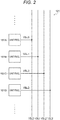
- Fig. 2 illustrates a main configuration example of the column pixel unit 121.
- a plurality of (for example, N (N is a natural number of 2 or more)) vertical signal lines is assigned to the column pixel unit 121.
- Each unit pixel of the column pixel unit 121 (that is, each unit pixel of the column of the pixel array) is connected to any of the plurality of vertical signal lines.
- the number of unit pixels included in the column pixel unit 121 is arbitrary.
- FIG. 2 In the case in Fig. 2 , four vertical signal lines (VSL0, VLS1, VSL2, and VSL3) are assigned, and four unit pixels (a unit pixel 151A, a unit pixel 151B, a unit pixel 151C, and a unit pixel 151D) are illustrated.
- the unit pixel 151A is connected to the vertical signal line VSL0.
- the unit pixel 151B is connected to the vertical signal line VSL1.
- the unit pixel 151C is connected to the vertical signal line VSL2.
- the unit pixel 151D is connected to the vertical signal line VSL3.
- the other unit pixels are similarly connected to any of the four vertical signal lines (VSL0, VLS1, VSL2, and VSL3).
- unit pixel(s) 151 in the case where there is no need to distinguish and describe the unit pixels from one another, they are simply referred to as unit pixel(s) 151. Furthermore, in the case where there is no need to distinguish and describe the vertical signal lines from one another, they are simply referred to as vertical signal line(s) VSL.
- Fig. 3 illustrates a main configuration example of the unit pixel 151.
- the unit pixel 151 includes a photodiode 161, a readout transistor 162, a reset transistor 163, an amplification transistor 164, and a select transistor 165.
- the photodiode 161 photoelectrically converts received light into a photocharge having a charge amount corresponding to a light amount of the received light and accumulates the photocharge.
- An anode electrode of the photodiode 161 is connected to a ground (pixel ground) of the pixel region, and a cathode electrode of the photodiode 161 is connected to a floating diffusion (FD) via the readout transistor 162.
- the readout transistor 162 controls readout of the photocharge from the photodiode 161.
- a drain electrode of the readout transistor 162 is connected to the floating diffusion, and a source electrode of the readout transistor 162 is connected to the cathode electrode of the photodiode 161.
- a control signal TRG is supplied from the pixel drive unit 142 to a gate electrode of the readout transistor 162.
- the reset transistor 163 resets a potential of the floating diffusion (FD).
- a drain electrode of the reset transistor 163 is connected to a power supply potential, and a source electrode of the reset transistor 163 is connected to the floating diffusion (FD).
- a control signal RST is supplied from the pixel drive unit 142 to a gate electrode of the reset transistor 163.
- the control signal RST that is, a gate potential of the reset transistor 163
- the floating diffusion (FD) is disconnected from the power supply potential.
- the control signal RST that is, the gate potential of the reset transistor 163
- the charge of the floating diffusion (FD) is discarded to the power supply potential, and the floating diffusion (FD) is reset.
- the amplification transistor 164 amplifies a potential change in the floating diffusion (FD) and outputs the amplified potential change as an electrical signal (analog signal).
- a gate electrode of the amplification transistor 164 is connected to the floating diffusion (FD)
- a drain electrode of the amplification transistor 164 is connected to the power supply potential
- a source electrode of the amplification transistor 164 is connected to a drain electrode of the select transistor 165.
- the amplification transistor 164 outputs the potential of the floating diffusion (FD) reset by the reset transistor 163 to the select transistor 165 as a reset signal (reset level).
- the amplification transistor 164 outputs the potential of the floating diffusion (FD), to which the photocharge has been transferred by the readout transistor 162, to the select transistor 165 as a light accumulation signal (signal level).
- the select transistor 165 controls output of the electrical signal supplied from the amplification transistor 164 to the vertical signal line VSL.
- a drain electrode of the select transistor 165 is connected to the source electrode of the amplification transistor 164 and a source electrode of the select transistor 165 is connected to the vertical signal line VSL.
- a control signal SEL is supplied from the pixel drive unit 142 to a gate electrode of the select transistor 165.
- the control signal SEL that is, a gate potential of the select transistor 165
- the amplification transistor 164 and the vertical signal line VSL are electrically disconnected.
- the pixel signal is not output from the unit pixel.
- the control signal SEL that is, the gate potential of the select transistor 165
- the unit pixel becomes selected. That is, the amplification transistor 164 and the vertical signal line VSL are electrically connected, and the signal output from the amplification transistor 164 is supplied to the vertical signal line VSL as the pixel signal of the unit pixel. That is, the pixel signal is read from the unit pixel.
- the configuration of the unit pixel 151 is arbitrary and is not limited to configuration illustrated in Fig. 3 .
- the readout transistor 162 may be omitted.
- the number of pixels per unit pixel is arbitrary, and may be one pixel as illustrated in Fig. 3 or may be a plurality of pixels.
- the unit pixel 151 includes four photodiodes 161 (a photodiode 161-0, a photodiode 161-1, a photodiode 161-2, and a photodiode 161-3).
- the unit pixel 151 is configured by four pixels.
- the photodiodes 161 may have the same characteristics as one another but may have the different characteristics from one another. For example, some or all of these photodiodes 161 may photoelectrically convert incident light in a wavelength band different from the others.
- the photodiodes 161-0 to 161-3 are arrayed in 2 rows and 2 columns.
- the photodiode 161-0 on the upper left in the 2 rows and 2 columns photoelectrically converts a red (R) band.
- the photodiode 161-1 on the upper right in the 2 rows and 2 columns photoelectrically converts a green (GR) band.
- the photodiode 161-2 on the lower left in the 2 rows and 2 columns photoelectrically converts a green (GB) band.
- the photodiode 161-3 on the lower right in the 2 rows and 2 columns photoelectrically converts a blue (B) band.
- the unit pixel 151 can form one unit of a Bayer array.
- the first embodiment is not limited to the Bayer array, and the same color may be shared by the floating diffusions (FD).
- the unit pixel 151 includes four read transistors 162 (a readout transistor 162-0, a readout transistor 162-1, a readout transistor 162-2, and a readout transistor 162-3).
- the readout transistor 162-0 controls readout of the photocharge from the photodiode 161-0 on the basis of the control signal TRG (TR0) supplied from the pixel drive unit 142.
- the readout transistor 162-1 controls readout of the photocharge from the photodiode 161-1 on the basis of the control signal TRG (TR1) supplied from the pixel drive unit 142.
- the readout transistor 162-2 controls readout of the photocharge from the photodiode 161-2 on the basis of the control signal TRG (TR2) supplied from the pixel drive unit 142.
- the readout transistor 162-3 controls readout of the photocharge from the photodiode 161-3 on the basis of the control signal TRG (TR3) supplied from the pixel drive unit 142.
- the configurations of the floating diffusion (FD), the reset transistor 163, the amplification transistor 164, the select transistor 165, and the like are shared in the unit pixel. Then, the pixel signals of the pixels (photodiode 161-0, photodiode 161-1, photodiode 161-2, and photodiode 161-3) are transmitted via the same vertical signal line VSL.
- the configuration of the unit pixel 151 will be described with reference to Fig. 4 .
- Fig. 5 is a diagram illustrating a main configuration example of the selection unit 122.
- a in Fig. 5 illustrates a configuration example of the selection unit 122A.
- B in Fig. 5 illustrates a configuration example of the selection unit 122B.
- the selection unit 122 is provided for each column pixel unit 121 and controls connection between the N vertical signal lines of the column pixel unit 121 and the M systems of A/D conversion units (M vertical signal lines) of the column A/D conversion unit 123.
- M vertical signal lines M vertical signal lines
- the selection unit 122A selects any two of the four vertical signal lines (VSL0 to VSL3) of the column pixel unit 121 corresponding to the selection unit 122A and connects the selected two vertical signal lines to the two vertical signal lines (VSLA0 and VSLA1) of the column A/D conversion unit 123A.
- the selection unit 122 may include a switch that switches the plurality of pixel signals output from the pixel array unit 111 for each control signal.
- the selection unit 122B has basically a similar configuration to the selection unit 122A. That is, in the case of the example in B in Fig. 5 , the selection unit 122B selects any two of the four vertical signal lines (VSL0, VSL1, VSL2, and VSL3) of the column pixel unit 121 corresponding to the selection unit 122B and connects the selected two vertical signal lines to the two vertical signal lines (VSLBO and VSLB1) of the column A/D conversion unit 123B.
- the selection unit 122 can switch the pixel signals of the plurality of pixels output by the pixel array unit 111 for each control signal.
- the selection unit 122 selects the vertical signal line VSL corresponding to a mode for outputting the pixel signal from among the plurality of vertical signal lines VSL assigned to the column.
- the control unit 131 causes the selection unit 122 to select one of the vertical signal lines VSL for each column. Then, the control unit 131 performs control such that the pixel signal from the pixel connected to the vertical signal line VSL selected by the selection unit 122 is output in that mode, and the output pixel signal is transmitted via the signal line selected by the selection unit 122.
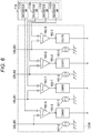
- Fig. 6 illustrates a main configuration example of the column A/D conversion unit 123B.
- the column A/D conversion unit 123 includes the M systems of A/D conversion units as described above.
- the column A/D conversion unit 123 includes four systems (VSLBO, VSLB1, VSLB2, and VSLB3) of A/D conversion units.
- the column A/D conversion unit 123B includes a current source 181-0, a comparator 182-0, and a counter 183-0, as the A/D conversion unit of the vertical signal line VSLB0 system.
- the current source 181-0 represents a load of a peripheral circuit connected to the vertical signal line VSLB0.
- the current source 181-0 is connected to the vertical signal line VSLB0 and the ground.
- the D/A conversion unit 113 supplies the ramp signal to each system of the column A/D conversion unit 123B.
- the D/A conversion unit 113 includes four D/A conversion units. Specifically, the D/A conversion unit 113 includes the D/A conversion unit 113A that supplies the ramp signal to the A/D conversion unit of the vertical signal line VSLB0 system, the D/A conversion unit 113B that supplies the ramp signal to the A/D conversion unit of the vertical signal line VSLB1 system, the D/A conversion unit 113C that supplies the ramp signal to the A/D conversion unit of the vertical signal line VSLB2 system, and the D/A conversion unit 113D that supplies the ramp signal to the A/D conversion unit of the vertical signal line VSLB3 system.
- the comparison unit 182-0 compares the pixel signal transmitted from the unit pixel 151 of the pixel array unit 111 via the vertical signal line VSL, the selection unit 122B, and the vertical signal line VSLB0 with the ramp signal supplied from the D/A conversion unit 113A, and supplies a comparison result (information indicating which of the values is larger) to the counter 183-0.
- the counter 183-0 counts a period from the start of counting to a change in a value of the comparison result, and outputs a count value to the horizontal transfer unit 124B as digital data of the pixel signal at the point of time when the value of the comparison result has changed.
- the column A/D conversion unit 123B includes a current source 181-1, a comparator 182-1, and a counter 183-1, as the A/D conversion unit of the vertical signal line VSLB1 system.
- the current source 181-1 has a similar configuration to the current source 181-0. That is, the current source 181-1 represents a load of a peripheral circuit connected to the vertical signal line VSLB1.
- the current source 181-1 is connected to the vertical signal line VSLB1 and the ground.
- the comparison unit 182-1 has a similar configuration to the comparison unit 182-0 and performs similar processing to the comparison unit 182-0. That is, the comparison unit 182-1 compares the pixel signal transmitted from the unit pixel 151 of the pixel array unit 111 via the vertical signal line VSL, the selection unit 122B, and the vertical signal line VSLB1 with the ramp signal supplied from the D/A conversion unit 113B, and supplies a comparison result (information indicating which of the values is larger) to the counter 183-1.
- the counter 183-1 has a similar configuration and performs similar processing to the counter 183-0. That is, the counter 183-1 counts a period from the start of counting to a change in a value of the comparison result, and outputs a count value to the horizontal transfer unit 124B as digital data of the pixel signal at the point of time when the value of the comparison result has changed.
- the column A/D conversion unit 123B includes a current source 181-2, a comparator 182-2, and a counter 183-2, as the A/D conversion unit of the vertical signal line VSLB1 system.
- the current source 181-2 has a similar configuration to the current source 181-0. That is, the current source 181-2 represents a load of a peripheral circuit connected to the vertical signal line VSLB1.
- the current source 181-2 is connected to the vertical signal line VSLB2 and the ground.
- the comparison unit 182-2 has a similar configuration to the comparison unit 182-0 and performs similar processing to the comparison unit 182-0. That is, the comparison unit 182-2 compares the pixel signal transmitted from the unit pixel 151 of the pixel array unit 111 via the vertical signal line VSL, the selection unit 122B, and the vertical signal line VSLB2 with the ramp signal supplied from the D/A conversion unit 113C, and supplies a comparison result (information indicating which of the values is larger) to the counter 183-2.
- the counter 183-2 has a similar configuration and performs similar processing to the counter 183-0. That is, the counter 183-2 counts a period from the start of counting to a change in a value of the comparison result, and outputs a count value to the horizontal transfer unit 124B as digital data of the pixel signal at the point of time when the value of the comparison result has changed.
- the column A/D conversion unit 123B includes a current source 181-3, a comparator 182-3, and a counter 183-3, as an A/D conversion unit of the vertical signal line VSLB3 system.
- the current source 181-3 has a similar configuration to the current source 181-0. That is, the current source 181-3 represents a load of a peripheral circuit connected to the vertical signal line VSLB3.
- the current source 181-3 is connected to the vertical signal line VSLB3 and the ground.
- the comparison unit 182-3 has a similar configuration to the comparison unit 182-0 and performs similar processing to the comparison unit 182-0. That is, the comparison unit 182-3 compares the pixel signal transmitted from the unit pixel 151 of the pixel array unit 111 via the vertical signal line VSL, the selection unit 122B, and the vertical signal line VSLB3 with the ramp signal supplied from the D/A conversion unit 113D, and supplies a comparison result (information indicating which of the values is larger) to the counter 183-3.
- the counter 183-3 has a similar configuration and performs similar processing to the counter 183-0. That is, the counter 183-3 counts a period from the start of counting to a change in a value of the comparison result, and outputs a count value to the horizontal transfer unit 124B as digital data of the pixel signal at the point of time when the value of the comparison result has changed.
- the column A/D conversion unit 123A also has a similar configuration and performs similar processing to the column A/D conversion unit 123B. That is, no matter how many configurations the column A/D conversion unit 123 has, each column A/D conversion unit 123 has a similar configuration and performs similar processing to the example in Fig. 6 .
- the number of systems of the A/D conversion units included in the column A/D conversion unit 123 is arbitrary, and may be one system or three or more systems. Regardless of the number of systems, the D/A conversion unit 113 can supply an independent ramp signal of each system. That is, for example, in the case where the column A/D conversion unit 123 includes M systems of A/D conversion units, independent M D/A conversion units 113 can be provided.
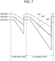
- Fig. 7 illustrates examples of the ramp signals output from the D/A conversion unit 113.
- the D/A conversion unit 113 generates and outputs the ramp signal under the control of the control unit 131.
- a gain of the ramp signal of the A/D conversion unit of the column A/D conversion unit 123 can be set using the slope of the ramp signal. For example, in a case where the slope of the ramp signal is small, the gain of the A/D conversion unit of the column A/D conversion unit 123 can be set to be large. On the other hand, in a case where the slope of the ramp signal is large, the gain of the A/D conversion unit of the column A/D conversion unit 123 can be set to be small.
- the D/A conversion unit 113 outputs the ramp signal twice for each readout of the pixel signal.
- a reset level (P phase) of the unit pixel 151 is read (this period is called P-phase readout period), and the pixel signal of the P-phase unit pixel 151 is A/D converted by the column A/D conversion unit 123.
- a signal (D phase) photoelectrically converted by the unit pixel 151 is read (this period is called D-phase readout period), and the pixel signal of the D-phase unit pixel 151 is A/D converted by the column A/D conversion unit 123.
- the slope of the ramp signal in the P-phase readout period and the slope of the ramp signal in the D-phase readout period are the same. Note that “upper” means an upper direction in Fig. 7 and “lower” means a lower direction in Fig. 7 unless otherwise specified.
- Fig. 7 illustrates that, for example, a ramp signal 1, a ramp signal 2, and a ramp signal 3 have different slopes from one another.
- the D-phase readout period can be shortened by making the slope steep while the D-phase readout period can be made long by making the slope gentle.
- the column A/D conversion unit 123B includes a comparison unit 182-0 and a counter 183-0 (see Fig. 6 ).
- the comparison unit 182-0 compares the magnitude of the pixel signal transmitted via the vertical signal line VSLB0 with the magnitude of the ramp signal supplied from the D/A conversion unit 113A. Then, the comparison unit 182-0 supplies a comparison result to the counter 183-0.
- the counter 183-0 counts a period from the start of comparison to a change in the comparison result in the comparison unit 182-0, and outputs a count value.
- the D-phase readout period becomes longer. Therefore, the gain of the A/D conversion unit of the column A/D conversion unit 123 can be set to be larger using the ramp signal 1 than using the ramp signal 2 and the ramp signal 3. Meanwhile, since the slope LA2 of the ramp signal 2 is larger than the slope LA1 of the ramp signal 1 and is smaller than the slope LA3 of the ramp signal 3, the D-phase readout period becomes a period between the ramp signal 1 and the ramp signal 3.
- the gain of the A/D conversion unit of the column A/D conversion unit 123 can be set to be larger using the ramp signal 2 than using the ramp signal 3 and to be smaller using the ramp signal 2 than using the ramp signal 1. Meanwhile, since the slope LA3 of the ramp signal 3 is larger than the slope LA1 of the ramp signal 1 and the slope LA2 of the ramp signal 2, the D-phase readout period becomes shorter. Therefore, the gain of the A/D conversion unit of the column A/D conversion unit 123 can be set to be smaller using the ramp signal 3 than using the ramp signal 1 and the ramp signal 2.
- the slopes are not limited to the three slopes.
- the slopes of the predetermined ramp signals can be set for the D/A conversion unit 113A, the D/A conversion unit 113B, the D/A conversion unit 113C, and the D/A conversion unit 113D, respectively.
- the D/A conversion unit 113 can set the gain for each system.
- the D/A conversion unit 113 can relatively shift offsets of the ramp signals 1, 2, and 3 in an up-down direction under the control of the control unit 131, as illustrated in Fig. 7 .
- the control unit 131 can prevent output data from including noise by relatively shifting the offsets of the ramp signals 1, 2, and 3 in the up-down direction.
- Fig. 8 illustrates a main configuration example of the address decoder 141.
- the address decoder 141 includes a logic circuit illustrated in Fig. 8 for each line of the pixel array. Then, control signals for specifying addresses such as an address for selecting a pixel (ADD_X), a readout latch reset (RLRST), a readout latch set (RLSET_X), an electronic shutter latch reset (SLRST), and an electronic shutter latch set (SLSET_X) are input from the sensor controller 131 to the address decoder 141.
- ADD_X address for selecting a pixel
- RLRST readout latch reset
- RLSET_X readout latch set
- SLRST electronic shutter latch reset
- SLSET_X electronic shutter latch set
- the address decoder 141 sets a value "H (high)" as a readout latch (RLQ) or an electronic shutter latch (SLQ) to the pixel drive unit 142 on the basis of the above input signals in the logic circuit of the line specified by the control unit 131.
- NOT_readout latch (XRLQ) and NOT _electronic shutter latch (XSLQ) are pulses in which the control signals have a negative logic.
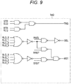
- Fig. 9 illustrates a main configuration example of the pixel drive unit 142.
- the pixel drive unit 142 includes a logic circuit illustrated in Fig. 9 for each line of the pixel array.
- the pixel drive unit 142 supplies the control signal TRG, the control signal SEL, and the control signal RST to the transistors of each unit pixel 151 of the appropriate line according to values of various control signals such as a readout latch output pulse RLQ and an electronic shutter latch SLQ supplied from the address decoder 141, and a readout transfer pulse RTR, an electronic shutter transfer pulse STR, an electronic shutter reset pulse SRST, a readout reset pulse RRST, and a readout select pulse RSEL supplied from the sensor controller 131.
- various control signals such as a readout latch output pulse RLQ and an electronic shutter latch SLQ supplied from the address decoder 141, and a readout transfer pulse RTR, an electronic shutter transfer pulse STR, an electronic shutter reset pulse SRST, a readout reset pulse RRST, and a readout select pulse RSEL supplied from the sensor controller 131.
- control unit 131 sets a range in the row direction and a range in the column direction to form a region, sets a plurality of (here, four) regions, and assigns the control signal for each of the four regions. For example, the control unit 131 assigns the A system control signal to the first region, the B system control signal to the second region, the C system control signal to the third region, and the D system control signal to the fourth region.
- Fig. 10 illustrates a concept of the control unit 131 controlling the unit pixel 151A, the unit pixel 151B, the unit pixel 151C, and the unit pixel 151D of the pixel array unit 111 in the solid-state imaging device 100 of the first embodiment.
- Fig. 10 is an explanatory diagram illustrating a concept of outputting the pixel signals of the unit pixel 151A, the unit pixel 151B, the unit pixel 151C, and the unit pixel 151D of the pixel array unit 111.
- the vertical scanning unit 132 is controlled by the control unit 131 to drive the unit pixels of each column of the pixel array unit 111 for each line and output the pixel signals. That is, the vertical scanning unit 132 outputs the pixel signals of a plurality of pixels in the range in the column direction set by the control unit 131, for each row and in the column direction.
- a pixel control signal CS1 controls the A system and causes the unit pixel 151A to output the pixel signal.
- a pixel control signal CS2 controls the B system and causes the unit pixel 151B to output the pixel signal.
- a pixel control signal CS3 controls the C system and causes the unit pixel 151C to output the pixel signal.
- a pixel control signal CS4 controls the D system and causes the unit pixel 151D to output the pixel signal.
- the readout unit 112 converts the pixel signals of the plurality of pixels in the range in the row direction set by the control unit 131 from analog signals into digital signals, for each column and in the row direction. That is, the readout unit 112 performs signal processing such as A/D conversion of the A system for the pixel signal output from the unit pixel 151A according to a control signal RS1 of the control unit 131, and outputs the signal.
- the readout unit 112 performs signal processing such as A/D conversion of the B system for the pixel signal output from the unit pixel 151B according to a control signal RS2 of the control unit 131, and outputs the signal.
- the readout unit 112 performs signal processing such as A/D conversion of the C system for the pixel signal read from the unit pixel 151C according to a control signal RS3 of the control unit 131, and outputs the signal.
- the readout unit 112 performs signal processing such as A/D conversion of the D system for the pixel signal read from the unit pixel 151D according to a control signal RS4 of the control unit 131, and outputs the signal.
- the control unit 131 can independently set a plurality of regions (regions of the A system to the D system).
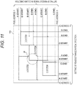
- Fig. 11 illustrates a concept in which the control unit 131 sets a region in the pixel array unit 111 for each pixel control signal.
- Fig. 11 is an explanatory diagram illustrating a concept of setting four regions of the A system to the D system in the pixel array unit 111.
- the direction from AD address 0 to X is the row direction
- the direction from pixel address 0 to Y is the column direction. Note that since the control unit 131 sets the range in the row direction and the column direction, the case where the start point and the end point are set oppositely is also included. In this case, the opposite directions of the row direction and the column direction are also included in the row direction and the column direction.
- the control unit 131 sets a range of outputting pixel signals from START of AD address A to END of the AD address A in the row direction, as the region of the A system. Furthermore, the control unit 131 sets a range of outputting the pixel signals from START of pixel address A to END of the pixel address A in the column direction. Thereby, the control unit 131 can set the region of the A system.
- control unit 131 sets a range of outputting pixel signals from START of AD address B to END of the AD address B in the row direction. Furthermore, the control unit 131 sets a range of outputting the pixel signals from START of pixel address B to END of the pixel address B in the column direction, as the region of the B system. Thereby, the control unit 131 can set the region of the B system.
- the control unit 131 sets a range of outputting pixel signals from START of AD address C to END of the AD address C in the row direction, as the region of the C system. Furthermore, the control unit 131 sets a range of outputting the pixel signals from START of pixel address C to END of the pixel address C in the column direction. Thereby, the control unit 131 can set the region of the C system.
- the control unit 131 sets a range of outputting pixel signals from START of AD address D to END of the AD address D in the row direction, as the region of the D system. Furthermore, the control unit 131 sets a range of outputting the pixel signals from START of pixel address D to END of the pixel address D in the column direction. Thereby, the control unit 131 can set the region of the D system.
- Fig. 12 illustrates a partially enlarged diagram of part of the region P where the region of the A system and the region of the B system overlap.
- Fig. 12 is a partially enlarged diagram of the overlapping region P.
- the plurality of unit pixels 151A, the plurality of unit pixels 151B, the plurality of unit pixels 151C, and the plurality of unit pixels 151D are arrayed in each row.
- a plurality of rows of the A system is controlled by the pixel control signal CS1 from the control unit 131.
- a plurality of rows of the B system is controlled by the pixel control signal CS2 from the control unit 131.
- control unit 131 performs control for each row and in the column direction, and the pixel array unit 111 outputs the pixel signals in the ranges in which the region of the A system and the region of the B system are set.
- control unit 131 can control two or more control signals to simultaneously output the pixel signals of the plurality of pixels corresponding to the two or more control signals in the range in the column direction set by the control unit 131. For example, in rows in which control of the A system and the control of the B system are adjacent to each other in the overlapping region P, two unit pixels 151A and two unit pixels 151B are output.
- the solid-state imaging device 100 can improve the resolution of the region P where the region of the A system and the region of the B system overlap.
- a pixel control signal CS1 of A system and a pixel control signal CS2 of B system will be described. Note that the same configuration as that of the solid-state imaging device 100 in the first embodiment is denoted by the same reference numeral, and redundant description is omitted as appropriate.
- Fig. 13 illustrates a concept of controlling a region of the A system and a region of the B system by the pixel control signal CS1 and the pixel control signal CS2.
- Fig. 13 is an explanatory diagram illustrating a control signal configuring the pixel control signal CS1 and the pixel control signal CS2.
- a signal line for transmitting the pixel control signal CS1 and the pixel control signal CS2 is connected to at least a reset transistor, an amplification transistor, and a select transistor.
- the pixel control signal CS1 and the pixel control signal CS2 are connected to a control signal TRG, a control signal SEL, and a control signal RST. That is, in the region of the A system, the pixel control signal CS1 is connected to a control signal TRGA1, a control signal SELA1, and a control signal RSTA1, and causes pixel signals of a plurality of pixels of the A system to be read out. That is, in the region of the B system, the pixel control signal CS2 is connected to a control signal TRGB1, a control signal SELB1, and a control signal RSTB1, and causes pixel signals of a plurality of pixels of the B system to be read out.
- a control unit 131 of a solid-state imaging device 100 can set an accumulation time for each of a plurality of regions. Specifically, the control unit 131 can set the accumulation time for each of the region of the A system, the region of the B system, a region of C system, and a region of D system by pixel control signals (the pixel control signal CS1, the pixel control signal CS2, a pixel control signal CS3, and a pixel control signal CS4).
- control unit 131 can set the accumulation times set for the plurality of respective regions (the region of the A system, the region of the B system, the region of the C system, and the region of the D system) to be different from one another or to be the same among the regions.
- the A system and the B system can be set to have long accumulation in which a photoelectric conversion element accumulates charges for a long time, as compared with the C system and the D system.
- control unit 131 can set the plurality of regions independently of one another. Specifically, the control unit 131 can independently set the region of the A system, the region of the B system, the region of the C system, and the region of the D system, and can control the region of the A system, the region of the B system, the region of the C system, and the region of the D system by the pixel control signals (the pixel control signal CS1, the pixel control signal CS2, a pixel control signal CS3, and a pixel control signal CS4), respectively. Thereby, the control unit 131 can individually control the accumulation time for photoelectric conversion for each region of the A system to the D system.
- the pixel control signal CS1, the pixel control signal CS2, a pixel control signal CS3, and a pixel control signal CS4 the control unit 131 can individually control the accumulation time for photoelectric conversion for each region of the A system to the D system.
- the number of pixel control signals CS1 and the number of pixel control signals CS2 are not limited to one in the A system and the B system.
- two systems of a pixel control signal CS1A1 and a pixel control signal CS1A2 may be provided, and two controls may be provided in the A system.
- the pixel control signal CS1A1 and the pixel control signal CS1A2 may have different accumulation times.
- Fig. 14 illustrates a concept of the control unit 131 of the solid-state imaging device 100 according to the second embodiment controlling a pixel array unit 111 independently for each system.
- Fig. 14 is an explanatory diagram illustrating a concept of controlling the pixel array unit 111 for each system.
- the A system and the B system in Fig. 14 have the same pixel address and AD address. Therefore, output pixels in the region of the A system and the region of the B system are doubled, and the resolution becomes high. Furthermore, the control unit 131 can control the pixel control signal CS1 of the A system and the pixel control signal CS2 of the B system to set longer accumulation than the regions of the C system and the D system.
- the regions of the C system and the D system have shorter accumulation by the pixel control signal CS3 and the pixel control signal CS4 than the regions of the A system and the B system.
- the control unit 131 can control the accumulation times of the A system, the B system, the C system, and the D system independently of one another.
- a plurality of unit pixels 151C of the C system and a plurality of unit pixels 151D of the D system can be output, respectively. Therefore, the resolution can be maximized by setting the output regions of the A system to the D system in the entire range.
- Fig. 15 illustrates a control example of setting the regions output in the A system to the D system in the entire range.
- Fig. 15 is an explanatory diagram illustrating a concept in which the four regions of the A system to the D system are set in an overlapping manner in the entire range of the pixel array unit 111.
- the control unit 131 sets a range of outputting pixel signals from START of AD address A to END of the AD address A in the row direction, as the region of the A system. Furthermore, the control unit 131 sets a range of outputting the pixel signals from START of pixel address A to END of the pixel address A in the column direction. Thereby, the control unit 131 can set the region of the A system.
- control unit 131 sets a range of outputting pixel signals from START of AD address B to END of the AD address B, which is the same address as the A system, in the row direction. Furthermore, the control unit 131 sets a range of outputting the pixel signals from START of pixel address B to END of the pixel address B, which is the same address as the A system, in the column direction as the region of the B system. Thereby, the control unit 131 can set the region of the B system, which is the same region as the A system.
- control unit 131 sets a range of outputting pixel signals from START of AD address C to END of the AD address C, which is the same address as the A system, in the row direction as the region of the C system. Furthermore, the control unit 131 sets a range of outputting the pixel signals from START of pixel address C to END of the pixel address C, which is the same address as the A system, in the column direction. Thereby, the control unit 131 can set the region of the C system, which is the same region as the A system.
- control unit 131 sets a range of outputting pixel signals from START of AD address D to END of the AD address D, which is the same address as the A system, in the row direction as the region of the D system. Furthermore, the control unit 131 sets a range of outputting the pixel signals from START of pixel address D to END of the pixel address D, which is the same address as the A system, in the column direction. Thereby, the control unit 131 can set the region of the D system, which is the same region as the A system.
- control unit 131 of the solid-state imaging device 100 can control the output of the pixel signals from the A system to the D system in the pixel array unit 111.
- the control unit 131 can output the pixel signals of the plurality of unit pixels (a plurality of unit pixels 151A, a plurality of unit pixels 151B, a plurality of unit pixels C, and a plurality of unit pixels D) of the A system to the D system. Therefore, an image with the maximum resolution can be obtained.
- the control unit 131 can set the accumulation times of the A system to the D system independently of one another.
- a control unit of the solid-state imaging device according to the third embodiment further sets, for each control signal, a gain for amplifying a signal converted by a column A/D converter into a digital signal, in addition to the control unit of the solid-state imaging device according to the first embodiment.
- the same configuration as that of the solid-state imaging device 100 in the first embodiment is denoted by the same reference numeral, and description is omitted as appropriate.
- Fig. 16 illustrates examples of ramp signals output from a D/A conversion unit 113.
- Fig. 16 illustrates that gain of a column A/D conversion unit 123 can be set according to a slope of a ramp signal.
- the D/A conversion unit 113 generates and outputs the ramp signal under control of a control unit 131.
- the gain of the ramp signal of the A/D conversion unit of the column A/D conversion unit 123 can be set using the slope of the ramp signal. For example, in a case where the slope of the ramp signal is small, the gain of the A/D conversion unit of the column A/D conversion unit 123 can be set to be large. On the other hand, in a case where the slope of the ramp signal is large, the gain of the A/D conversion unit of the column A/D conversion unit 123 can be set to be small. Furthermore, the D/A conversion unit 113 outputs the ramp signal twice for each readout of the pixel signal.
- a reset level (P phase) of a unit pixel 151 is read (this period is called P-phase readout period), and the pixel signal of the P-phase unit pixel 151 is A/D converted by the column A/D conversion unit 123.
- a signal (D phase) photoelectrically converted by the unit pixel 151 is read (this period is called D-phase readout period), and the pixel signal of the D-phase unit pixel 151 is A/D converted by the column A/D conversion unit 123.
- the slope of the ramp signal in the P-phase readout period and the slope of the ramp signal in the D-phase readout period are the same. Note that "upper” means an upper direction in Fig. 16 and “lower” means a lower direction in Fig. 16 unless otherwise specified.
- Fig. 16 illustrates that, for example, a ramp signal 1, a ramp signal 2, and a ramp signal 3 have different slopes from one another.
- the D-phase readout period can be shortened by making the slope steep while the D-phase readout period can be made long by making the slope gentle.
- a column A/D conversion unit 123B includes a comparison unit 182-0 and a counter 183-0 (see Fig. 6 ).
- the comparison unit 182-0 compares the magnitude of the pixel signal transmitted via a vertical signal line VSLB0 with the magnitude of the ramp signal supplied from a D/A conversion unit 113A. Then, the comparison unit 182-0 supplies a comparison result to the counter 183-0.
- the counter 183-0 counts a period from the start of comparison to a change in the comparison result in the comparison unit 182-0, and outputs a count value.
- the D-phase readout period becomes longer. Therefore, the gain of the A/D conversion unit of the column A/D conversion unit 123 can be set to be larger using the ramp signal 1 than using the ramp signal 2 and the ramp signal 3. Meanwhile, since the slope LA2 of the ramp signal 2 is larger than the slope LA1 of the ramp signal 1 and is smaller than the slope LA3 of the ramp signal 3, the D-phase readout period becomes a period between the ramp signal 1 and the ramp signal 3.
- the gain of the A/D conversion unit of the column A/D conversion unit 123 can be set to be larger using the ramp signal 2 than using the ramp signal 3 and to be smaller using the ramp signal 2 than using the ramp signal 1. Meanwhile, since the slope LA3 of the ramp signal 3 is larger than the slope LA1 of the ramp signal 1 and the slope LA2 of the ramp signal 2, the D-phase readout period becomes shorter. Therefore, the gain of the A/D conversion unit of the column A/D conversion unit 123 can be set to be smaller using the ramp signal 3 than using the ramp signal 1 and the ramp signal 2.
- the D/A conversion unit 113 supplies the ramp signals as illustrated in Fig. 16 to the column A/D conversion unit 123.
- the column A/D conversion unit 123 can change the gain according to the slopes (slope LA1, slope LA2, and slope LA3) of the ramp signals from the D/A conversion unit 113.
- the D/A conversion unit 113 includes the D/A conversion unit 113A, a D/A conversion unit 113B, a D/A conversion unit 113C, and a D/A conversion unit 113D for respective systems from A system to D system, the gains can be respectively set for the A system to the D system.
- the control unit 131 can set a first predetermined gain in the A system. Furthermore, in the D/A conversion unit 113B the control unit 131 can set a second predetermined gain in the B system. Furthermore, in the D/A conversion unit 113C the control unit 131 can set a third predetermined gain in the C system. Furthermore, in the D/A conversion unit 113D the control unit 131 can set a fourth predetermined gain in the D system. Note that the number of D/A conversion units 113 is not limited to four and the number of D/A conversion units 113 may be reduced by sharing them. Furthermore, the method of changing the gain is not limited thereto, and various methods can be applied.
- the D/A conversion unit 113 can relatively shift offsets of the ramp signals 1, 2, and 3 in an up-down direction under the control of the control unit 131, as illustrated in Fig. 16 .
- the control unit 131 can prevent output data from including noise by relatively shifting the offsets of the ramp signals 1, 2, and 3 in the up-down direction.
- a switch configured to switch, for each control signal, pixel signals of a plurality of pixels output from a pixel array unit 111, is further included in the solid-state imaging device according to the first embodiment.
- a selection unit 122 includes a switch will be described. Note that the same configuration as that of the solid-state imaging device 100 in the first embodiment is denoted by the same reference numeral, and description is omitted as appropriate.
- Fig. 17 illustrates a configuration of the solid-state imaging device according to the fourth embodiment, which further includes VSL switches SW (VSL switch SW1, VSL switch SW2, VSL switch SW3, VSL switch SW4, VSL switch SW5, VSL switch SW6, VSL switch SW7, and VSL switch SW8).
- Fig. 17 is an explanatory diagram illustrating the solid-state imaging device including the VSL switches SW1 to SW8.
- Fig. 17 illustrates a configuration of the solid-state imaging device including two systems of A system and B system.
- a vertical scanning unit 132 is controlled by a control unit 131 to drive unit pixels of each column of a pixel array unit 111 for each line and output the pixel signals.
- a pixel control signal CS1 controls the A system and causes a unit pixel 151A to output the pixel signal.
- a pixel control signal CS2 controls the B system and causes a unit pixel 151B to output the pixel signal.
- Unit pixels 151C to 151H are assumed to output pixel signals according to the pixel control signal CS1 or the pixel control signal CS2.
- VSL switches SW1 to SW8 are provided in the selection unit 122.
- the VSL switches SW1 to SW8 are controlled on the basis of control signals for controlling the VSL switches SW1 to SW8.
- a column A/D conversion unit 123 is controlled on the basis of a control signal RS1 corresponding to the pixel control signal CS1 and a control signal RS2 corresponding to the pixel control signal CS2.
- Fig. 18 illustrates a conceptual diagram in a case where there is no switching operation of the VSL switches SW1 to SW8.
- Fig. 18 is an explanatory diagram illustrating a state in which switching of the VSL switches SW1 to SW8 is fixed and the switching operation of the VSL switches SW1 to SW8 is not performed.
- a column A/D conversion unit 123A and a column A/D conversion unit 123B output the pixel signals of pixels in each row of the A system or the B system.
- the control unit causes a first A/D converter to convert pixel signals of pixels corresponding to first control for controlling at least some even rows into digital signals and causes a second A/D converter to convert pixel signals of pixels corresponding to second control for controlling at least some odd rows into digital signals, and causes the first A/D converter and the second A/D converter to output the pixel signals of the pixels, respectively.
- control unit switches the switch to cause the second A/D converter to convert the pixel signals of the pixels corresponding to the first control for controlling even rows into digital signals and cause the first A/D converter to convert the pixel signals of the pixels corresponding to the second control for controlling odd rows into digital signals, and cause the first A/D converter and the second A/D converter to output the pixel signals of the pixels, respectively.
- the pixel signals of the pixels corresponding to the first control and the pixel signals of the pixels corresponding to the second control can be alternately output in units of rows, whereby the resolution can be improved.
- Fig. 19 illustrates switching of the VSL switches SW1 to SW8 for alternately outputting the pixel signals of the pixels corresponding to the first control and the pixel signals of the pixels corresponding to the second control in units of rows.
- Fig. 19 is an explanatory diagram illustrating switching of the VSL switches SW1 to SW8 of the solid-state imaging device according to the fourth embodiment.
- the control unit 131 switches the VSL switches SW1 to SW8, so that a readout unit 112 can switch the column A/D conversion unit 123A and the column A/D conversion unit 123B to alternately output the pixels signals in units of rows.
- the column A/D conversion unit 123A outputs a unit pixel 151A, a unit pixel 151C, a unit pixel 151F, and a unit pixel 151H.
- the column A/D conversion unit 123B outputs a unit pixel 151B, a unit pixel 151D, a unit pixel 151E, and a unit pixel 151D.
- control unit 131 switches the VSL switches SW1 to SW8, so that the column A/D conversion unit 123A outputs the unit pixel 151B, the unit pixel 151D, the unit pixel 151E, and the unit pixel 151G.
- the column A/D conversion unit 123B outputs the unit pixel 151A, the unit pixel 151C, the unit pixel 151F, and the unit pixel 151H.
- the pixel signals of the pixels corresponding to the first control and the pixel signals of the pixels corresponding to the second control can be alternately output from the pixel array unit 111 in units of rows.
- the solid-state imaging device according to the fourth embodiment of the present technology can improve the resolution of an image in a set region.
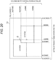
- Fig. 20 illustrates a state in which the pixel array unit 111 outputs pixel signals of pixels of the A system and the B system.
- Fig. 20 is an explanatory diagram illustrating a concept of alternately outputting even rows and odd rows in the A system and the B system of the pixel array unit 111.
- the pixel signals of the pixels of the A system and the B system can be alternately output for each row, whereby the resolution can be improved in the pixel array unit 111.
- a region Q where the region of the A system and the region of the B system overlap has the same resolution as the non-overlapping region.
- the VSL switches SW1 to SW8 are provided, the pixel signals of the pixels of one system are output when the other system of the two systems is being output.
- the pixel signals can be alternately output for each row.
- Fig. 21 illustrates a concept of outputting pixel signals of pixels of one system while being outputting pixel signals of the other system of two systems.
- Fig. 21 is an explanatory diagram illustrating a case in which the pixel signals of the pixels of a certain row of the B system is being output, the VSL switches SW1 to SW8 are switched to partially output pixel signals of pixels of the A system.
- Fig. 21A illustrates a case where the pixel signals of the pixels of the A system and the B system are output for each row in the overlapping region Q in Fig. 20 .
- Fig. 21B the pixel signal of the pixel of the A system is output to part of the pixel signals of the pixels of the B system, and the pixel signal of the pixel of the B system is interpolated in the output signal of the A system.
- the solid-state imaging device can alternately output the pixel signals of the pixels of the A system and the B system for each row by using the VSL switches SW1 to SW8. Furthermore, the solid-state imaging device according to the fourth embodiment of the present technology can interpolate the pixel signals of adjacent pixels by switching the VSL switches SW1 to SW8, thereby improving the resolution.
- a control unit switches a switch to output a pixel signal of a pixel corresponding to first control by a control signal for performing the first control, or output a pixel signal of a pixel corresponding to second control by a control signal for performing the second control, among pixels corresponding to both control of the first control and the second control, in the solid-state imaging device according to the fourth embodiment.
- the same configuration as that of the fifth embodiment is denoted by the same reference numeral, and description is omitted as appropriate.
- Fig. 22 illustrates a concept of outputting pixels corresponding to both the first control and the second control as pixel signals of pixels both of A system and B system.
- Fig. 22 is an explanatory diagram illustrating a state in which a control unit 131 switches VSL switches SW1 to SW8 to output pixel signals of the same pixels of both the A system and the B system.
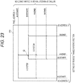
- Fig. 23 illustrates a concept in which a pixel array unit 111 can read pixel signals of the same pixels both of the A system and the B system.
- Fig. 23 is an explanatory diagram illustrating a state of outputting the pixel signals of the same pixels of both the A system and the B system. In the case in Fig. 23 , in a region Q where the A system and the B system overlap, the pixel signals of the pixels of the A system and the pixel signals of the pixels of the B system can be output.
- Fig. 24 illustrates a concept of outputting the pixels of the pixel signals both of the A system and the B system.
- Fig. 24 is an explanatory diagram illustrating a state in which the control unit 131 switches the VSL switches SW1 to SW8 to output pixel signals of the same pixels of both the A system and the B system.
- a region of the A system and a region of the B system can output the pixel signals of the same pixels both as the A system and the B system. Note that, in this case, the same pixels are output and thus accumulation times need to match. Furthermore, in the region Q where the region of the A system and the region of the B system overlap, the pixel signals can be output as both the A system and the B system. Note that, in the fifth embodiment, a frame rate decreases because the number of outputting pixel signals increases.
- a control unit can set a standby mode of not allowing conversion into a digital signal, for at least some of the plurality of column A/D conversion units, in association with some of a plurality of regions, in the solid-state imaging device according to the first embodiment.
- a control unit can set a standby mode of not allowing conversion into a digital signal, for at least some of the plurality of column A/D conversion units, in association with some of a plurality of regions, in the solid-state imaging device according to the first embodiment.
- Fig. 25 illustrates a state in which a control unit 131 sets a standby mode of not allowing some of column A/D conversion units 123 to convert pixels signals into digital signals.
- Fig. 25 is an explanatory diagram illustrating a state of setting the standby mode in the column A/D conversion units 123.
- a selection unit 122 includes VSL switches SW1 to SW4.
- VSL switches SW1 to SW4 Four vertical signal lines (VSL0, VLS1, VSL2, and VSL3) are connected to a column A/D conversion unit A, a column A/D conversion unit 123B, a column A/D conversion unit 123C, and a column A/D conversion unit 123D via VSL switches SW1 to SW4 in a constant manner.
- the control unit 131 controls the column A/D conversion unit 123A by a control signal RS1 corresponding to a pixel control signal CS1. Furthermore, the control unit 131 controls the column A/D conversion unit 123B by a control signal RS2 corresponding to a pixel control signal CS2. Furthermore, the control unit 131 controls the column A/D conversion unit 123C by a control signal RS3 corresponding to a pixel control signal CS3. Furthermore, the control unit 131 controls the column A/D conversion unit 123D by a control signal RS4 corresponding to a pixel control signal CS4.
- control unit 131 sets the standby mode of not allowing conversion into a digital signal, for at least some of the plurality of column A/D conversion units 123, in association with some of a plurality of regions.
- Fig. 26 illustrates an example in which the control unit 131 sets only the column A/D conversion unit 123A among the plurality of column A/D conversion units 123 to be enabled to convert pixel signals into digital signals.
- Fig. 26 is an explanatory diagram illustrating that the column A/D conversion unit 123B, the column A/D conversion unit 123C, and the column A/D conversion unit 123D are set to the standby mode of not performing processing of converting pixel signals into digital signals.
- the column A/D conversion unit 123 only the column A/D conversion unit 123A can execute digital conversion processing.
- the column A/D conversion unit 123B, the column A/D conversion unit 123C, and the column A/D conversion unit 123D cannot perform the digital conversion processing, so all the signals supposed to be output from the column A/D conversion unit 123B, the column A/D conversion unit 123C, and column A/D conversion unit 123D are output from the column A/D conversion unit 123A.
- Fig. 27 illustrates a concept of outputting pixel signals of pixels from the column A/D conversion unit 123A as the A system in a pixel array unit 111.
- Fig. 27 is an explanatory diagram illustrating a state of outputting pixel signals of pixels only in the A system.
- the control unit 131 sets long time as accumulation time of the A system, for example, and also sets a gain of the column A/D conversion unit 123A to be high.
- control unit 131 sets a range of outputting pixel signals from START of AD address A to END of the AD address A in a row direction, as a region of the A system. Furthermore, the control unit 131 sets a range of outputting the pixel signals from START of pixel address A to END of the pixel address A in the column direction. As a result, the control unit 131 can output the pixel signals of the pixels in the region of the A system from the column A/D conversion unit 123A.
- the solid-state imaging device 100 can suppress power consumption.
- control unit 131 can set the two column A/D conversion unit 123C and column A/D conversion unit 123D among the plurality of column A/D conversion units 123 to the standby mode of not allowing conversion into digital signals.
- Fig. 28 illustrates a state in which the two column A/D conversion units 123A and 123B are enabled, and the other column A/D conversion units 123C and 123D are set to the standby mode.
- Fig. 28 is an explanatory diagram illustrating the state in which the standby mode of not allowing digital conversion processing is set for the column A/D conversion unit 123C and the column A/D conversion unit 123D.
- the selection unit 122 always connects the vertical signal line VSL0 or the vertical signal line VSL2 to the column A/D conversion unit 123A, and always connects the vertical signal line VSL1 or the vertical signal line VSL3 to the column A/D conversion unit 123B. Thereby, the pixel array unit 111 can output pixel signals of pixels from the column A/D conversion unit 123A and the column A/D conversion unit 123B.
- Fig. 29 illustrates a concept of outputting pixel signals of pixels from the column A/D conversion unit 123A and the column A/D conversion unit 123B in the A system and the B system in the pixel array unit 111.
- Fig. 29 is an explanatory diagram illustrating a state in which pixel signals of pixels are output from the column A/D conversion unit 123A and the column A/D conversion unit 123B.
- the column A/D conversion unit 123 can output the pixel signals of the pixels of the A system with the gain of the column A/D conversion unit 123A and can output the pixel signals of the pixels of the B system with the gain of the column A/D conversion unit 123B. Since the column A/D conversion unit 123C corresponding to the region of the C system and the column A/D conversion unit 123D corresponding to the region of the D system are in the standby mode, the solid-state imaging device 100 can suppress power consumption.
- An electronic device is an electronic device in which a solid-state imaging device is mounted, the solid-state imaging device including a pixel array in which a plurality of pixels is two-dimensionally arrayed in a row direction and a column direction, a control unit configured to set a range to output pixel signals of the plurality of pixels in the pixel array to each of the row direction and the column direction, a vertical scanning unit configured to output the pixel signals of the plurality of pixels in the range in the column direction set by the control unit, for each row and in the column direction, and a column A/D converter configured to convert the pixel signals of the plurality of pixels in the range in the row direction set by the control unit from analog signals into digital signals, for each column and in the row direction.
- the electronic device may be an electronic device equipped with any one of the solid-state imaging devices according to the first to sixth embodiments of the present technology.
- Fig. 30 is a diagram illustrating use examples of one of the solid-state imaging devices according to the first to sixth embodiments of the present technology as an image sensor.
- the above-described solid-state imaging devices according to the first to sixth embodiments can be used in various cases for sensing light such as visible light, infrared light, ultraviolet light, and X-ray, as will be described below, for example. That is, as illustrated in Fig. 30 , one of the solid-state imaging devices according to the first to sixth embodiments can be used as a device (for example, as the electronic device according to the fifth embodiment) in the field of appreciation in which images to be provided for use in appreciation are captured, in the field of transportation, the field of home appliances, the field of medical and healthcare, the field of security, the field of beauty, the field of sports, or the field of agriculture, for example.
- one of the solid-state imaging devices according to the first to sixth embodiments can be used as a device for capturing an image to be provided for appreciation, such as a digital camera, a smart phone, or a mobile phone device having a camera function, for example.
- one of the solid-state imaging devices according to the first to sixth embodiments can be used as a device provided for use in traffic, such as an in-vehicle sensor that captures the front, rear, surroundings, and an interior of the vehicle for safe driving such as automatic stop, recognition of a driver's state, a monitoring camera that monitors traveling vehicles and roads, or a distance measuring sensor that measures a distance between vehicles, for example.
- a device provided for use in traffic such as an in-vehicle sensor that captures the front, rear, surroundings, and an interior of the vehicle for safe driving such as automatic stop, recognition of a driver's state, a monitoring camera that monitors traveling vehicles and roads, or a distance measuring sensor that measures a distance between vehicles, for example.
- one of the solid-state imaging devices according to the first to sixth embodiments can be used as a device provided for home appliances such as a TV receiver, a refrigerator, or an air conditioner, for capturing a gesture of a user and performing a device operation according to the gesture, for example.
- a device provided for home appliances such as a TV receiver, a refrigerator, or an air conditioner, for capturing a gesture of a user and performing a device operation according to the gesture, for example.
- one of the solid-state imaging devices according to the first to sixth embodiments can be used as a device provided for use in medical and healthcare, such as an endoscope or a device that performs angiography by receiving infrared light, for example.
- one of the solid-state imaging devices according to the first to sixth embodiments can be used as a device provided for use in security, such as a monitoring camera for crime prevention or a camera for person authentication use, for example.
- one of the solid-state imaging devices according to the first to sixth embodiments can be used as a device provided for use in beauty, such as a skin measuring instrument that captures skin or a microscope that captures scalp, for example.
- one of the solid-state imaging devices according to the first to sixth embodiments can be used as a device provided for use in sports, such as an action camera or a wearable camera for sport use, for example.
- one of the solid-state imaging devices according to the first to sixth embodiments can be used as a device provided for use in agriculture, such as a camera for monitoring the condition of fields and crops, for example.
- the above-described solid-state imaging device 100 can be applied to every type of electronic device having an imaging function, such as a camera system of a digital still camera or a video camera, or a mobile phone having an imaging function.
- Fig. 31 illustrates a schematic configuration of an electronic device 102 (camera) as an example.
- the electronic device 102 is, for example, a video camera capable of capturing a still image or a moving image, and includes a solid-state imaging device 101, an optical system (optical lens) 310, a shutter device 311, and a drive unit 313 that drives the solid-state imaging device 101 and the shutter device 311, and a signal processing unit 312.
- the optical system 310 guides image light (incident light) from an object to a pixel unit 101a of the solid-state imaging device 101.
- the optical system 310 may be configured by a plurality of optical lenses.
- the shutter device 311 controls a light irradiation period and a light shielding period for the solid-state imaging device 101.
- the drive unit 313 controls a transfer operation of the solid-state imaging device 101 and a shutter operation of the shutter device 311.
- the signal processing unit 312 performs various types of signal processing for a signal output from the solid-state imaging device 101.
- a video signal Dout after the signal processing is stored in a storage medium such as a memory or is output to a monitor or the like.
- first to sixth embodiments of the present technology are not limited to the above-described embodiments, and various changes can be made without departing from the gist of the present technology.
- the present technology can employ the following configurations.
Landscapes
- Engineering & Computer Science (AREA)
- Multimedia (AREA)
- Signal Processing (AREA)
- Transforming Light Signals Into Electric Signals (AREA)
Abstract
Description
- The present technology relates to a solid-state imaging device and an electronic device equipped with the solid-state imaging device, and particularly relates to a technology of a solid-state imaging device capable of more easily acquiring data in an imaging region.
- In recent years, solid-state imaging devices (image sensors) that are principal components of digital cameras have been increased in demand. For example, it is considered to read pixel signals configuring image data from pixels at a high speed for each column in a solid-state imaging device having a complementary metal oxide semiconductor (CMOS) image sensor.
- At the same time, the image data output from the solid-state imaging device is required to have various output formats due to improvement in information processing technology. Therefore, for example, a technique relating to a solid-state imaging device capable of supporting various output formats has also been studied (see Patent Document 1).
- Patent Document 1: International Publication No.
2015/133323 - By the way, in a pixel array in which a plurality of pixels is two-dimensionally arranged, even if a range to output the pixel signals in a column direction can be set as an imaging region, a range to output the pixel signals in a row direction has been difficult to set.
- Therefore, the present technology has been made in view of the foregoing and a principal object of the present technology is to provide a solid-state imaging device enabling output of a pixel signal in a row direction and capable of individually setting an imaging region and an electronic device equipped with the solid-state imaging device.
- As a result of earnest research to solve the above-described object, the present inventor has succeeded in setting an imaging region in a pixel array and has reached completion of the present technology.
- That is, the present technology first provides a solid-state imaging device including:
- a pixel array in which a plurality of pixels is two-dimensionally arrayed in a row direction and a column direction;
- a control unit configured to set a range to output pixel signals of the plurality of pixels in the pixel array to each of the row direction and the column direction;
- a vertical scanning unit configured to output the pixel signals of the plurality of pixels in the range in the column direction set by the control unit, for each row and in the column direction; and
- a column A/D converter configured to convert the pixel signals of the plurality of pixels in the range in the row direction set by the control unit from analog signals into digital signals, for each column and in the row direction.
- In the solid-state imaging device according to the present technology, at least two or more control signals for outputting the pixel signals of the plurality of pixels may be assigned for each row, and
the control unit
may set the range in the row direction and the range in the column direction to form a region and
may set a plurality of the regions and assigns the control signals to the plurality of respective regions. - In the solid-state imaging device according to the present technology, the control unit
may set an accumulation time for accumulation for each of the plurality of regions. In this case, the control unit may set the accumulation times set for the respective regions of the plurality of regions to be different from one another or to be same among the regions. - In the solid-state imaging device according to the present technology, the control unit
may control the two or more control signals to simultaneously output the pixel signals of the plurality of pixels corresponding to the two or more control signals in the range in the column direction set by the control unit. - In the solid-state imaging device according to the present technology, the control unit
may set the plurality of regions independently of one another. - In the solid-state imaging device according to the present technology, a signal line for transmitting the control signal may be connected to at least a reset transistor, an amplification transistor, and a select transistor.
- In the solid-state imaging device according to the present technology, a switch configured to switch, for the each control signal, the pixel signals of the plurality of pixels output from the pixel array, may be further included. Furthermore, in the present technology, a selection unit configured to select a signal line for supplying the pixel signals of the plurality of pixels to the column/AD conversion unit may be further included, and
the selection unit may include the switch, and
may switch, for the each control signal, the pixel signals of the plurality of pixels output from the pixel array. - In this case, the control unit may switch the switch to
cause a first A/D converter to convert the pixel signals of the pixels corresponding to first control for controlling at least some even rows into digital signals and cause a second A/D converter to convert the pixel signals of the pixels corresponding to second control for controlling at least some odd rows into digital signals, and cause the first A/D converter and the second A/D converter to output the pixel signals of the pixels, respectively, and
next, cause the second A/D converter to convert the pixel signals of the pixels corresponding to the first control into digital signals and cause the first A/D converter to convert the pixel signals of the pixels corresponding to the second control into digital signals, and cause the first A/D converter and the second A/D converter to output the pixel signals of the pixels, respectively. - Moreover, in the present technology,
the control unit may switch the switch to
output the pixel signal of the pixel corresponding to the first control by the control signal for performing the first control, or output the pixel signal of the pixel corresponding to the second control by the control signal for performing the second control, from among the pixels corresponding to both control of the first control and the second control. - In the solid-state imaging device according to the present technology, a plurality of the column A/D conversion units may be further included, and
the control unit
may set a standby mode of not allowing conversion into the digital signal, for at least some of the plurality of column A/D conversion units in association with some of the plurality of regions. - In the solid-state imaging device according to the present technology, the control unit
may set, for the each control signal, a gain that amplifies the digital signal converted by the column A/D converter. - Furthermore, the present technology provides an electronic device in which a solid-state imaging device is mounted,
the solid-state imaging device including: - a pixel array in which a plurality of pixels is two-dimensionally arrayed in a row direction and a column direction;
- a control unit configured to set a range to output pixel signals of the plurality of pixels in the pixel array to each of the row direction and the column direction;
- a vertical scanning unit configured to output the pixel signals of the plurality of pixels in the range in the column direction set by the control unit, for each row and in the column direction; and
- a column A/D converter configured to convert the pixel signals of the plurality of pixels in the range in the row direction set by the control unit from analog signals into digital signals, for each column and in the row direction.
- According to the present technology, the image quality of a captured image can be improved by setting an imaging region. Note that effects of the present technology are not limited to the above-described effects, and any of effects described in the present disclosure may be exhibited.
-
-
Fig. 1 is a block diagram illustrating a main configuration example of an image sensor to which the present technology is applied. -
Fig. 2 is a diagram illustrating a main configuration example of a column pixel unit. -
Fig. 3 is a diagram illustrating a main configuration example of a unit pixel. -
Fig. 4 is a diagram illustrating another configuration example of the unit pixel. -
Fig. 5 is a diagram illustrating a main configuration example of a selection unit. -
Fig. 6 is a diagram illustrating a main configuration example of a column A/D conversion unit. -
Fig. 7 is a graph illustrating examples of ramp signals output from a D/A conversion unit. -
Fig. 8 is a diagram illustrating a main configuration example of an address decoder. -
Fig. 9 is a diagram illustrating a main configuration example of a pixel drive unit. -
Fig. 10 is an explanatory diagram illustrating a concept of outputting pixel signals of unit pixels of a pixel array unit. -
Fig. 11 is an explanatory diagram illustrating a concept of setting four regions of A system to D system in the pixel array unit. -
Fig. 12 is a partially enlarged diagram of an overlapping region. -
Fig. 13 is an explanatory diagram illustrating a control signal configuring a pixel control signal. -
Fig. 14 is an explanatory diagram illustrating a concept of controlling the pixel array unit for each system. -
Fig. 15 is an explanatory diagram illustrating a concept in which the four regions of the A system to the D system are set in an overlapping manner in the entire range of the pixel array unit. -
Fig. 16 is a graph illustrating examples of ramp signals output from the D/A conversion unit. -
Fig. 17 is an explanatory diagram illustrating a solid-state imaging device including VSL switches. -
Fig. 18 is an explanatory diagram illustrating a state in which no switching operations of the VSL switches are performed. -
Fig. 19 is an explanatory diagram illustrating switching operations of the VSL switches. -
Fig. 20 is an explanatory diagram illustrating a concept of alternately outputting even rows and odd rows in the A system and the B system of the pixel array unit. -
Fig. 21 is explanatory diagrams illustrating a state of switching the VSL switches and outputting a pixel signal of a pixel in the A system to some output of the B system. -
Fig. 22 is an explanatory diagram illustrating a state in which a control unit can switch the VSL switches to output the same pixel of both the A system and the B system. -
Fig. 23 is an explanatory diagram illustrating a state of outputting pixel signals of the same pixels of both the A system and the B system. -
Fig. 24 is an explanatory diagram illustrating a state in which the control unit can switch the VSL switches to output the pixel signals of the same pixels of both the A system and the B system. -
Fig. 25 is an explanatory diagram illustrating a state of setting a standby mode in the column A/D conversion unit. -
Fig. 26 is an explanatory diagram illustrating a state of setting the standby mode of not allowing some column A/D conversion unit to perform digital conversion processing. -
Fig. 27 is an explanatory diagram illustrating a state of outputting pixel signals of pixels only in the A system. -
Fig. 28 is an explanatory diagram illustrating a state of setting the standby mode of not allowing digital conversion processing in two column A/D conversion units. -
Fig. 29 is an explanatory diagram illustrating a state of outputting pixel signals of pixels from two column A/D conversion units. -
Fig. 30 is a diagram illustrating use examples of the solid-state imaging device of the first to sixth embodiments to which the present technology is applied. -
Fig. 31 is a functional block diagram of an example of an electronic device to which the present technology is applied. - Hereinafter, favorable embodiments for implementing the present technology will be described with reference to the drawings. Note that the embodiments described below describe examples of a representative embodiment of the present technology, and the scope of the present technology is not construed in a narrow manner by the embodiments.
- Note that the description will be given in the following order.
- 1. Outline of Present Technology
- 2. First Embodiment (Example 1 of Solid-State Imaging Device)
- 3. Second Embodiment (Example 2 of Solid-State Imaging Device)
- 4. Third Embodiment (Example 3 of Solid-State Imaging Device)
- 5. Fourth Embodiment (Example 4 of Solid-State Imaging Device)
- 6. Fifth Embodiment (Example 5 of Solid-State Imaging Device)
- 7. Sixth Embodiment (Example 6 of Solid-State Imaging Device)
- 8. Seventh Embodiment Regarding Electronic Device
- 9. Use Example of Solid-State Imaging Device To Which Present Technology is Applied
- First, an outline of the present technology will be described. The present technology relates to an electronic device equipped with a solid-state imaging device that sets a range of outputting pixel signals of a plurality of pixels in a pixel array in a row direction and a column direction, and setting an imaging region, and an electronic device equipped with the solid-state imaging device. According to the present technology, the image quality of a captured image can be improved.
- A solid-state imaging device has included a vertical scanning unit, and has caused the vertical scanning unit to output a pixel signal of a pixel by controlling an address in the column direction. Meanwhile, in the row direction, the solid-state imaging device has outputted a pixel signal and then an image processing circuit in a subsequent stage and connected to the solid-state imaging device has cut out an image in the row direction.
- Here, since the solid-state imaging device has not controlled a range of outputting pixel signals in the row direction, the solid-state imaging device has not been able to freely set the range of outputting pixel signals of pixels in a pixel array.
- The present technology has been made in view of the above circumstances and has enabled setting of an imaging region in a pixel array. Thereby, the present technology can improve the image quality of a captured image captured by the solid-state imaging device.
- A solid-state imaging device according to a first embodiment of the present technology is a solid-state imaging device including a pixel array in which a plurality of pixels is two-dimensionally arrayed in a row direction and a column direction, a control unit configured to set a range to output pixel signals of the plurality of pixels in the pixel array to each of the row direction and the column direction, a vertical scanning unit configured to output the pixel signals of the plurality of pixels in the range in the column direction set by the control unit, for each row and in the column direction, and a column A/D converter configured to convert the pixel signals of the plurality of pixels in the range in the row direction set by the control unit from analog signals into digital signals, for each column and in the row direction.
- The solid-state imaging device according to the first embodiment of the present technology can set the range to output pixel signals in the row direction and the column direction, thereby improving the image quality of a captured image.
-
Fig. 1 illustrates a solid-state imaging device 100 as an example of the solid-state imaging device according to the first embodiment of the present technology.Fig. 1 is a block diagram illustrating a partial configuration example of a complementary metal oxide semiconductor (CMOS) image sensor as an embodiment of a solid-state imaging device to which the present technology is applied. Note that "upper" means an upper direction inFig. 1 and "lower" means a lower direction inFig. 1 unless otherwise specified. - The solid-
state imaging device 100 illustrated inFig. 1 is an imaging device that captures an image of an object and obtains digital data of a captured image. Note that a CMOS image sensor will be described as an example in the present specification. However, the present technology can also be applied to an imaging device other than a CMOS image sensor, such as a charge coupled device (CCD) image sensor. - As illustrated in
Fig. 1 , the solid-state imaging device 100 includes apixel array unit 111, areadout unit 112A, areadout unit 112B, acontrol unit 131, avertical scanning unit 132, ahorizontal scanning unit 133, and a D/A conversion unit 113. - The
pixel array unit 111 has a plurality of pixels two-dimensionally arranged in the row direction and the column direction. Thepixel array unit 111 is a pixel region in which pixel configurations (unit pixels) each having a photoelectric conversion element such as a photodiode are arranged in a planar manner. Each unit pixel of thepixel array unit 111 receives light from the object, photoelectrically converts incident light, and accumulates a charge. Then, each unit pixel of thepixel array unit 111 outputs the charge as a pixel signal at predetermined timing. - A signal line (vertical signal line) that transfers the pixel signal is assigned to each column of the unit pixels. Furthermore, an operation regarding readout of the pixel signals are controlled for each line (row) of the unit pixels.
- The
pixel array unit 111 includes acolumn pixel unit 121 that is a configuration for one column of the unit pixels as many as the number of columns.Fig. 1 illustrates only the configuration for one column, but thepixel array unit 111 has P (P is a natural number)column pixel units 121 in a case where thepixel array unit 111 has P columns of unit pixels, for example. Thecolumn pixel unit 121 has a plurality of (for example, N (N is a natural number of 2 or more)) signal lines (vertical signal lines) for transmitting pixel signals output from the unit pixels of the column. That is, thecolumn pixel unit 121 can output a plurality of (for example, N) pixel signals in parallel. - The
control unit 131 has a function to set a range to output the pixel signals of a plurality of pixels in thepixel array unit 111 in the row direction and the column direction. Furthermore, thecontrol unit 131 has a function to control an operation of each processing unit of the solid-state imaging device 100. Thecontrol unit 131 controls thevertical scanning unit 132 and thehorizontal scanning unit 133 to output the pixel signals from thepixel array unit 111. - The
vertical scanning unit 132 outputs the pixel signals of a plurality of pixels in the range in the column direction set by thecontrol unit 131, for each row and in the column direction. That is, thevertical scanning unit 132 is controlled by thecontrol unit 131 to drive the unit pixels of each column of thepixel array unit 111 for each line and output the pixel signals. Furthermore, thevertical scanning unit 132 includes anaddress decoder 141 and apixel drive unit 142. - The
address decoder 141 decodes address specifying information supplied from thecontrol unit 131 and supplies a control signal to the configuration corresponding to the specified address of thepixel drive unit 142. - The
pixel drive unit 142 is controlled by thecontrol unit 131 to supply a control signal for driving each unit pixel of thepixel array unit 111. Thepixel drive unit 142 has a configuration to supply the control signal for each line of thepixel array unit 111. Thepixel drive unit 142 supplies the control signal corresponding to control content specified by thecontrol unit 131 to each unit pixel of the specified line of thepixel array unit 111, using the configuration specified by theaddress decoder 141. Note that this control signal may also be hereinafter referred to as a pixel control signal. - The
readout unit 112A reads the pixel signal from thepixel array unit 111, performs signal processing such as A/D conversion, and outputs the pixel signal. Thereadout unit 112A includes aselection unit 122A and a column A/D conversion unit 123A for each column (each column pixel unit 121) of thepixel array unit 111.Fig. 1 illustrates only the configuration for one column, but thereadout unit 112A includes P (P is a natural number)selection units 122A and P column A/D conversion units 123A in the case where thepixel array unit 111 has P columns of unit pixels, for example. - The
selection unit 122A selects a signal line for supplying the pixel signal to the column/AD conversion unit 123A from among a plurality of (for example, N) vertical signal lines of thecolumn pixel unit 121 corresponding to theselection unit 122A. In this case, theselection unit 122A controls connection between the vertical signal line of the column pixel unit 121 (the unit pixels connected to the vertical signal line) and the column A/D conversion unit 123A. - The column A/
D conversion unit 123A converts the pixel signals of a plurality of pixels in the range in the row direction set by thecontrol unit 131 from analog signals into digital signals, for each column and in the row direction. In this case, the column A/D conversion unit 123A performs A/D conversion for the pixel signals (analog data) transmitted from thecolumn pixel unit 121 via theselection unit 122A corresponding to the column A/D conversion unit 123A. The column A/D conversion unit 123A includes a plurality (for example, M (M is a natural number of 2 or more, where M ≤ N)) A/D conversion units and can perform A/D conversion for a plurality (for example, M) pixel signals transmitted via theselection unit 122A in parallel. Thereby, theselection unit 122A can select, for example, M vertical signal lines from among the N lines and connect the M vertical signal lines to the column A/D conversion unit 123A. - The column A/
D conversion unit 123A performs the A/D conversion for the pixel signals using a ramp signal supplied from the D/A conversion unit 113. Details will be described below. Furthermore, thereadout unit 112A includes ahorizontal transfer unit 124A. - The
horizontal transfer unit 124A sequentially outputs the pixel signals (digital data) output from each column A/D conversion unit 123A, that is, the pixel signals of each column of thepixel array unit 111. For example, in a case where thepixel array unit 111 includes P columns of unit pixels and each column A/D conversion unit 123A includes M A/D conversion units, P × M pixel signals are supplied in parallel to thehorizontal transfer unit 124A. Thehorizontal transfer unit 124A sequentially transmits the P × M pixel signals. The pixel signals output from thehorizontal transfer unit 124A are supplied to, for example, a processing unit (not illustrated) such as a signal processing unit connected in a subsequent stage. The processing unit in the subsequent stage may be provided inside the solid-state imaging device 100 or may be provided outside the solid-state imaging device 100. - The
readout unit 112B is a processing unit that performs similar processing to thereadout unit 112A and has a similar configuration to thereadout unit 112A. That is, thereadout unit 112B includes aselection unit 122B and a column A/D conversion unit 123B for each column of the unit pixels of thepixel array unit 111. Theselection unit 122B is a processing unit that performs similar processing to theselection unit 122A and has a similar configuration to theselection unit 122A. The column A/D conversion unit 123B is a processing unit that performs similar processing to the column A/D conversion unit 123A and has a similar configuration to the column A/D conversion unit 123A. Thereadout unit 112B includes ahorizontal transfer unit 124B. Thehorizontal transfer unit 124B is a processing unit that performs similar processing to thehorizontal transfer unit 124A and has similar configuration to thehorizontal transfer unit 124A. - Hereinafter, in the case where there is no need to distinguish and describe the
readout unit 112A and thereadout unit 112B from each other, they are simply referred to as readout unit(s) 112. Similarly, in the case where there is no need to distinguish and describe theselection unit 122A and theselection unit 122B from each other, they are simply referred to as selection unit(s) 122. Similarly, in the case where there is no need to distinguish and describe the column A/D conversion unit 123A and the column A/D conversion unit 123B from each other, they are simply referred to as column A/D conversion unit(s) 123. Similarly, in the case where there is no need to distinguish and describe thehorizontal transfer unit 124A and thehorizontal transfer unit 124B from each other, they are simply referred to as horizontal transfer unit(s) 124. - The D/
A conversion unit 113 supplies a predetermined ramp signal to the column A/D conversion unit 123. The D/A conversion unit 113 includes, as an example, four D/A conversion units, that is, a D/A conversion unit 113A, a D/A conversion unit 113B, a D/A conversion unit 113C, and a D/A conversion unit 113D. Therefore, the D/A conversion unit 113 can supply four ramp signals. Note that the D/A conversion unit 113 is not limited to the four D/A conversion units 113 and can be changed according to the number of ramp signals. - The above-described solid-
state imaging device 100 according to the first embodiment illustrated inFig. 1 includes two systems of paths for outputting the pixel signals from thepixel array unit 111. That is, in the case ofFig. 1 , thereadout unit 112 includes thereadout unit 112A and thereadout unit 112B. The number of routes is arbitrary and may be one system or three or more systems. Hereinafter, the case of two systems and the case of four systems will be appropriately described. -
Fig. 2 illustrates a main configuration example of thecolumn pixel unit 121. As described above, a plurality of (for example, N (N is a natural number of 2 or more)) vertical signal lines is assigned to thecolumn pixel unit 121. Each unit pixel of the column pixel unit 121 (that is, each unit pixel of the column of the pixel array) is connected to any of the plurality of vertical signal lines. Furthermore, the number of unit pixels included in thecolumn pixel unit 121 is arbitrary. - In the case in
Fig. 2 , four vertical signal lines (VSL0, VLS1, VSL2, and VSL3) are assigned, and four unit pixels (aunit pixel 151A, aunit pixel 151B, aunit pixel 151C, and aunit pixel 151D) are illustrated. Theunit pixel 151A is connected to the vertical signal line VSL0. Theunit pixel 151B is connected to the vertical signal line VSL1. Theunit pixel 151C is connected to the vertical signal line VSL2. Theunit pixel 151D is connected to the vertical signal line VSL3. In a case where thecolumn pixel unit 121 includes five or more unit pixels, the other unit pixels are similarly connected to any of the four vertical signal lines (VSL0, VLS1, VSL2, and VSL3). - Note that, hereinafter, in the case where there is no need to distinguish and describe the unit pixels from one another, they are simply referred to as unit pixel(s) 151. Furthermore, in the case where there is no need to distinguish and describe the vertical signal lines from one another, they are simply referred to as vertical signal line(s) VSL.
-
Fig. 3 illustrates a main configuration example of theunit pixel 151. As illustrated inFig. 3 , theunit pixel 151 includes aphotodiode 161, areadout transistor 162, areset transistor 163, anamplification transistor 164, and aselect transistor 165. - The
photodiode 161 photoelectrically converts received light into a photocharge having a charge amount corresponding to a light amount of the received light and accumulates the photocharge. An anode electrode of thephotodiode 161 is connected to a ground (pixel ground) of the pixel region, and a cathode electrode of thephotodiode 161 is connected to a floating diffusion (FD) via thereadout transistor 162. - The
readout transistor 162 controls readout of the photocharge from thephotodiode 161. A drain electrode of thereadout transistor 162 is connected to the floating diffusion, and a source electrode of thereadout transistor 162 is connected to the cathode electrode of thephotodiode 161. Furthermore, a control signal TRG is supplied from thepixel drive unit 142 to a gate electrode of thereadout transistor 162. When the control signal TRG (that is, a gate potential of the readout transistor 162) is in an OFF state, the photocharge is not read from the photodiode 161 (the photocharge is accumulated in the photodiode 161). When the control signal TRG (that is, the gate potential of the readout transistor 162) is in an ON state, the photocharge accumulated in thephotodiode 161 is read out and supplied to the floating diffusion (FD). - The
reset transistor 163 resets a potential of the floating diffusion (FD). A drain electrode of thereset transistor 163 is connected to a power supply potential, and a source electrode of thereset transistor 163 is connected to the floating diffusion (FD). Furthermore, a control signal RST is supplied from thepixel drive unit 142 to a gate electrode of thereset transistor 163. When the control signal RST (that is, a gate potential of the reset transistor 163) is in the OFF state, the floating diffusion (FD) is disconnected from the power supply potential. When the control signal RST (that is, the gate potential of the reset transistor 163) is in the ON state, the charge of the floating diffusion (FD) is discarded to the power supply potential, and the floating diffusion (FD) is reset. - The
amplification transistor 164 amplifies a potential change in the floating diffusion (FD) and outputs the amplified potential change as an electrical signal (analog signal). A gate electrode of theamplification transistor 164 is connected to the floating diffusion (FD), a drain electrode of theamplification transistor 164 is connected to the power supply potential, and a source electrode of theamplification transistor 164 is connected to a drain electrode of theselect transistor 165. For example, theamplification transistor 164 outputs the potential of the floating diffusion (FD) reset by thereset transistor 163 to theselect transistor 165 as a reset signal (reset level). Furthermore, theamplification transistor 164 outputs the potential of the floating diffusion (FD), to which the photocharge has been transferred by thereadout transistor 162, to theselect transistor 165 as a light accumulation signal (signal level). - The
select transistor 165 controls output of the electrical signal supplied from theamplification transistor 164 to the vertical signal line VSL. A drain electrode of theselect transistor 165 is connected to the source electrode of theamplification transistor 164 and a source electrode of theselect transistor 165 is connected to the vertical signal line VSL. Furthermore, a control signal SEL is supplied from thepixel drive unit 142 to a gate electrode of theselect transistor 165. When the control signal SEL (that is, a gate potential of the select transistor 165) is in the OFF state, theamplification transistor 164 and the vertical signal line VSL are electrically disconnected. - Therefore, in the OFF state, the pixel signal is not output from the unit pixel. When the control signal SEL (that is, the gate potential of the select transistor 165) is in the ON state, the unit pixel becomes selected. That is, the
amplification transistor 164 and the vertical signal line VSL are electrically connected, and the signal output from theamplification transistor 164 is supplied to the vertical signal line VSL as the pixel signal of the unit pixel. That is, the pixel signal is read from the unit pixel. - Note that the configuration of the
unit pixel 151 is arbitrary and is not limited to configuration illustrated inFig. 3 . For example, thereadout transistor 162 may be omitted. Furthermore, the number of pixels per unit pixel is arbitrary, and may be one pixel as illustrated inFig. 3 or may be a plurality of pixels. - Here, the configuration example of the unit pixel having a plurality of pixels is illustrated in
Fig. 4 . In the example inFig. 4 , theunit pixel 151 includes four photodiodes 161 (a photodiode 161-0, a photodiode 161-1, a photodiode 161-2, and a photodiode 161-3). In this case, theunit pixel 151 is configured by four pixels. Thephotodiodes 161 may have the same characteristics as one another but may have the different characteristics from one another. For example, some or all of thesephotodiodes 161 may photoelectrically convert incident light in a wavelength band different from the others. - For example, the photodiodes 161-0 to 161-3 are arrayed in 2 rows and 2 columns. In this case, the photodiode 161-0 on the upper left in the 2 rows and 2 columns photoelectrically converts a red (R) band. Furthermore, the photodiode 161-1 on the upper right in the 2 rows and 2 columns photoelectrically converts a green (GR) band. Furthermore, the photodiode 161-2 on the lower left in the 2 rows and 2 columns photoelectrically converts a green (GB) band. Furthermore, the photodiode 161-3 on the lower right in the 2 rows and 2 columns photoelectrically converts a blue (B) band. Thereby, the
unit pixel 151 can form one unit of a Bayer array. - Note that the first embodiment is not limited to the Bayer array, and the same color may be shared by the floating diffusions (FD).
- Furthermore, in the case in
Fig. 4 , theunit pixel 151 includes four read transistors 162 (a readout transistor 162-0, a readout transistor 162-1, a readout transistor 162-2, and a readout transistor 162-3). - The readout transistor 162-0 controls readout of the photocharge from the photodiode 161-0 on the basis of the control signal TRG (TR0) supplied from the
pixel drive unit 142. The readout transistor 162-1 controls readout of the photocharge from the photodiode 161-1 on the basis of the control signal TRG (TR1) supplied from thepixel drive unit 142. The readout transistor 162-2 controls readout of the photocharge from the photodiode 161-2 on the basis of the control signal TRG (TR2) supplied from thepixel drive unit 142. The readout transistor 162-3 controls readout of the photocharge from the photodiode 161-3 on the basis of the control signal TRG (TR3) supplied from thepixel drive unit 142. - In the case in
Fig. 4 , the configurations of the floating diffusion (FD), thereset transistor 163, theamplification transistor 164, theselect transistor 165, and the like are shared in the unit pixel. Then, the pixel signals of the pixels (photodiode 161-0, photodiode 161-1, photodiode 161-2, and photodiode 161-3) are transmitted via the same vertical signal line VSL. In the following description, the configuration of theunit pixel 151 will be described with reference toFig. 4 . -
Fig. 5 is a diagram illustrating a main configuration example of theselection unit 122. A inFig. 5 illustrates a configuration example of theselection unit 122A. B inFig. 5 illustrates a configuration example of theselection unit 122B. Theselection unit 122 is provided for eachcolumn pixel unit 121 and controls connection between the N vertical signal lines of thecolumn pixel unit 121 and the M systems of A/D conversion units (M vertical signal lines) of the column A/D conversion unit 123. In the case of the example in A inFig. 5 , theselection unit 122A selects any two of the four vertical signal lines (VSL0 to VSL3) of thecolumn pixel unit 121 corresponding to theselection unit 122A and connects the selected two vertical signal lines to the two vertical signal lines (VSLA0 and VSLA1) of the column A/D conversion unit 123A. Theselection unit 122 may include a switch that switches the plurality of pixel signals output from thepixel array unit 111 for each control signal. - The
selection unit 122B has basically a similar configuration to theselection unit 122A. That is, in the case of the example in B inFig. 5 , theselection unit 122B selects any two of the four vertical signal lines (VSL0, VSL1, VSL2, and VSL3) of thecolumn pixel unit 121 corresponding to theselection unit 122B and connects the selected two vertical signal lines to the two vertical signal lines (VSLBO and VSLB1) of the column A/D conversion unit 123B. - That is, the
selection unit 122 can switch the pixel signals of the plurality of pixels output by thepixel array unit 111 for each control signal. In each column, theselection unit 122 selects the vertical signal line VSL corresponding to a mode for outputting the pixel signal from among the plurality of vertical signal lines VSL assigned to the column. At that time, thecontrol unit 131 causes theselection unit 122 to select one of the vertical signal lines VSL for each column. Then, thecontrol unit 131 performs control such that the pixel signal from the pixel connected to the vertical signal line VSL selected by theselection unit 122 is output in that mode, and the output pixel signal is transmitted via the signal line selected by theselection unit 122. -
Fig. 6 illustrates a main configuration example of the column A/D conversion unit 123B. The column A/D conversion unit 123 includes the M systems of A/D conversion units as described above. In the case inFig. 6 , the column A/D conversion unit 123 includes four systems (VSLBO, VSLB1, VSLB2, and VSLB3) of A/D conversion units. Then, the column A/D conversion unit 123B includes a current source 181-0, a comparator 182-0, and a counter 183-0, as the A/D conversion unit of the vertical signal line VSLB0 system. The current source 181-0 represents a load of a peripheral circuit connected to the vertical signal line VSLB0. The current source 181-0 is connected to the vertical signal line VSLB0 and the ground. - The D/
A conversion unit 113 supplies the ramp signal to each system of the column A/D conversion unit 123B. In the case inFig. 6 , the D/A conversion unit 113 includes four D/A conversion units. Specifically, the D/A conversion unit 113 includes the D/A conversion unit 113A that supplies the ramp signal to the A/D conversion unit of the vertical signal line VSLB0 system, the D/A conversion unit 113B that supplies the ramp signal to the A/D conversion unit of the vertical signal line VSLB1 system, the D/A conversion unit 113C that supplies the ramp signal to the A/D conversion unit of the vertical signal line VSLB2 system, and the D/A conversion unit 113D that supplies the ramp signal to the A/D conversion unit of the vertical signal line VSLB3 system. - The comparison unit 182-0 compares the pixel signal transmitted from the
unit pixel 151 of thepixel array unit 111 via the vertical signal line VSL, theselection unit 122B, and the vertical signal line VSLB0 with the ramp signal supplied from the D/A conversion unit 113A, and supplies a comparison result (information indicating which of the values is larger) to the counter 183-0. - The counter 183-0 counts a period from the start of counting to a change in a value of the comparison result, and outputs a count value to the
horizontal transfer unit 124B as digital data of the pixel signal at the point of time when the value of the comparison result has changed. - The column A/
D conversion unit 123B includes a current source 181-1, a comparator 182-1, and a counter 183-1, as the A/D conversion unit of the vertical signal line VSLB1 system. The current source 181-1 has a similar configuration to the current source 181-0. That is, the current source 181-1 represents a load of a peripheral circuit connected to the vertical signal line VSLB1. The current source 181-1 is connected to the vertical signal line VSLB1 and the ground. - The comparison unit 182-1 has a similar configuration to the comparison unit 182-0 and performs similar processing to the comparison unit 182-0. That is, the comparison unit 182-1 compares the pixel signal transmitted from the
unit pixel 151 of thepixel array unit 111 via the vertical signal line VSL, theselection unit 122B, and the vertical signal line VSLB1 with the ramp signal supplied from the D/A conversion unit 113B, and supplies a comparison result (information indicating which of the values is larger) to the counter 183-1. - The counter 183-1 has a similar configuration and performs similar processing to the counter 183-0. That is, the counter 183-1 counts a period from the start of counting to a change in a value of the comparison result, and outputs a count value to the
horizontal transfer unit 124B as digital data of the pixel signal at the point of time when the value of the comparison result has changed. - The column A/
D conversion unit 123B includes a current source 181-2, a comparator 182-2, and a counter 183-2, as the A/D conversion unit of the vertical signal line VSLB1 system. The current source 181-2 has a similar configuration to the current source 181-0. That is, the current source 181-2 represents a load of a peripheral circuit connected to the vertical signal line VSLB1. The current source 181-2 is connected to the vertical signal line VSLB2 and the ground. - The comparison unit 182-2 has a similar configuration to the comparison unit 182-0 and performs similar processing to the comparison unit 182-0. That is, the comparison unit 182-2 compares the pixel signal transmitted from the
unit pixel 151 of thepixel array unit 111 via the vertical signal line VSL, theselection unit 122B, and the vertical signal line VSLB2 with the ramp signal supplied from the D/A conversion unit 113C, and supplies a comparison result (information indicating which of the values is larger) to the counter 183-2. - The counter 183-2 has a similar configuration and performs similar processing to the counter 183-0. That is, the counter 183-2 counts a period from the start of counting to a change in a value of the comparison result, and outputs a count value to the
horizontal transfer unit 124B as digital data of the pixel signal at the point of time when the value of the comparison result has changed. - The column A/
D conversion unit 123B includes a current source 181-3, a comparator 182-3, and a counter 183-3, as an A/D conversion unit of the vertical signal line VSLB3 system. The current source 181-3 has a similar configuration to the current source 181-0. That is, the current source 181-3 represents a load of a peripheral circuit connected to the vertical signal line VSLB3. The current source 181-3 is connected to the vertical signal line VSLB3 and the ground. - The comparison unit 182-3 has a similar configuration to the comparison unit 182-0 and performs similar processing to the comparison unit 182-0. That is, the comparison unit 182-3 compares the pixel signal transmitted from the
unit pixel 151 of thepixel array unit 111 via the vertical signal line VSL, theselection unit 122B, and the vertical signal line VSLB3 with the ramp signal supplied from the D/A conversion unit 113D, and supplies a comparison result (information indicating which of the values is larger) to the counter 183-3. - The counter 183-3 has a similar configuration and performs similar processing to the counter 183-0. That is, the counter 183-3 counts a period from the start of counting to a change in a value of the comparison result, and outputs a count value to the
horizontal transfer unit 124B as digital data of the pixel signal at the point of time when the value of the comparison result has changed. - The column A/
D conversion unit 123A also has a similar configuration and performs similar processing to the column A/D conversion unit 123B. That is, no matter how many configurations the column A/D conversion unit 123 has, each column A/D conversion unit 123 has a similar configuration and performs similar processing to the example inFig. 6 . - Note that the number of systems of the A/D conversion units included in the column A/
D conversion unit 123 is arbitrary, and may be one system or three or more systems. Regardless of the number of systems, the D/A conversion unit 113 can supply an independent ramp signal of each system. That is, for example, in the case where the column A/D conversion unit 123 includes M systems of A/D conversion units, independent M D/Aconversion units 113 can be provided. -
Fig. 7 illustrates examples of the ramp signals output from the D/A conversion unit 113. The D/A conversion unit 113 generates and outputs the ramp signal under the control of thecontrol unit 131. Here, a gain of the ramp signal of the A/D conversion unit of the column A/D conversion unit 123 can be set using the slope of the ramp signal. For example, in a case where the slope of the ramp signal is small, the gain of the A/D conversion unit of the column A/D conversion unit 123 can be set to be large. On the other hand, in a case where the slope of the ramp signal is large, the gain of the A/D conversion unit of the column A/D conversion unit 123 can be set to be small. Furthermore, the D/A conversion unit 113 outputs the ramp signal twice for each readout of the pixel signal. In the first output of the ramp signal, a reset level (P phase) of theunit pixel 151 is read (this period is called P-phase readout period), and the pixel signal of the P-phase unit pixel 151 is A/D converted by the column A/D conversion unit 123. In the second output of the ramp signal, a signal (D phase) photoelectrically converted by theunit pixel 151 is read (this period is called D-phase readout period), and the pixel signal of the D-phase unit pixel 151 is A/D converted by the column A/D conversion unit 123. Furthermore, the slope of the ramp signal in the P-phase readout period and the slope of the ramp signal in the D-phase readout period are the same. Note that "upper" means an upper direction inFig. 7 and "lower" means a lower direction inFig. 7 unless otherwise specified. -
Fig. 7 illustrates that, for example, aramp signal 1, aramp signal 2, and aramp signal 3 have different slopes from one another. As for the slope of the ramp signal, the D-phase readout period can be shortened by making the slope steep while the D-phase readout period can be made long by making the slope gentle. For example, the column A/D conversion unit 123B includes a comparison unit 182-0 and a counter 183-0 (seeFig. 6 ). The comparison unit 182-0 compares the magnitude of the pixel signal transmitted via the vertical signal line VSLB0 with the magnitude of the ramp signal supplied from the D/A conversion unit 113A. Then, the comparison unit 182-0 supplies a comparison result to the counter 183-0. The counter 183-0 counts a period from the start of comparison to a change in the comparison result in the comparison unit 182-0, and outputs a count value. - Therefore, for example, since a slope LA1 of the
ramp signal 1 is smaller than a slope LA2 of theramp signal 2 and a slope LA3 of theramp signal 3, the D-phase readout period becomes longer. Therefore, the gain of the A/D conversion unit of the column A/D conversion unit 123 can be set to be larger using theramp signal 1 than using theramp signal 2 and theramp signal 3. Meanwhile, since the slope LA2 of theramp signal 2 is larger than the slope LA1 of theramp signal 1 and is smaller than the slope LA3 of theramp signal 3, the D-phase readout period becomes a period between theramp signal 1 and theramp signal 3. Therefore, the gain of the A/D conversion unit of the column A/D conversion unit 123 can be set to be larger using theramp signal 2 than using theramp signal 3 and to be smaller using theramp signal 2 than using theramp signal 1. Meanwhile, since the slope LA3 of theramp signal 3 is larger than the slope LA1 of theramp signal 1 and the slope LA2 of theramp signal 2, the D-phase readout period becomes shorter. Therefore, the gain of the A/D conversion unit of the column A/D conversion unit 123 can be set to be smaller using theramp signal 3 than using theramp signal 1 and theramp signal 2. - Note that, in the D/
A conversion unit 113, the slopes (slopes LA1, LA2, and LA3) are not limited to the three slopes. The slopes of the predetermined ramp signals can be set for the D/A conversion unit 113A, the D/A conversion unit 113B, the D/A conversion unit 113C, and the D/A conversion unit 113D, respectively. Thereby, the D/A conversion unit 113 can set the gain for each system. Furthermore, the D/A conversion unit 113 can relatively shift offsets of the ramp signals 1, 2, and 3 in an up-down direction under the control of thecontrol unit 131, as illustrated inFig. 7 . Thecontrol unit 131 can prevent output data from including noise by relatively shifting the offsets of the ramp signals 1, 2, and 3 in the up-down direction. -
Fig. 8 illustrates a main configuration example of theaddress decoder 141. Theaddress decoder 141 includes a logic circuit illustrated inFig. 8 for each line of the pixel array. Then, control signals for specifying addresses such as an address for selecting a pixel (ADD_X), a readout latch reset (RLRST), a readout latch set (RLSET_X), an electronic shutter latch reset (SLRST), and an electronic shutter latch set (SLSET_X) are input from thesensor controller 131 to theaddress decoder 141. Theaddress decoder 141 sets a value "H (high)" as a readout latch (RLQ) or an electronic shutter latch (SLQ) to thepixel drive unit 142 on the basis of the above input signals in the logic circuit of the line specified by thecontrol unit 131. NOT_readout latch (XRLQ) and NOT _electronic shutter latch (XSLQ) are pulses in which the control signals have a negative logic. -
Fig. 9 illustrates a main configuration example of thepixel drive unit 142. Thepixel drive unit 142 includes a logic circuit illustrated inFig. 9 for each line of the pixel array. - The
pixel drive unit 142 supplies the control signal TRG, the control signal SEL, and the control signal RST to the transistors of eachunit pixel 151 of the appropriate line according to values of various control signals such as a readout latch output pulse RLQ and an electronic shutter latch SLQ supplied from theaddress decoder 141, and a readout transfer pulse RTR, an electronic shutter transfer pulse STR, an electronic shutter reset pulse SRST, a readout reset pulse RRST, and a readout select pulse RSEL supplied from thesensor controller 131. - Next, region control in which the solid-
state imaging device 100 according to the first embodiment of the present technology independently controls four systems and generates an image will be described. - In the first embodiment, at least two or more control signals for outputting the pixel signals of a plurality of pixels are assigned to each row. The
control unit 131 sets a range in the row direction and a range in the column direction to form a region, sets a plurality of (here, four) regions, and assigns the control signal for each of the four regions. For example, thecontrol unit 131 assigns the A system control signal to the first region, the B system control signal to the second region, the C system control signal to the third region, and the D system control signal to the fourth region. -
Fig. 10 illustrates a concept of thecontrol unit 131 controlling theunit pixel 151A, theunit pixel 151B, theunit pixel 151C, and theunit pixel 151D of thepixel array unit 111 in the solid-state imaging device 100 of the first embodiment.Fig. 10 is an explanatory diagram illustrating a concept of outputting the pixel signals of theunit pixel 151A, theunit pixel 151B, theunit pixel 151C, and theunit pixel 151D of thepixel array unit 111. - As illustrated in
Fig. 10 , thevertical scanning unit 132 is controlled by thecontrol unit 131 to drive the unit pixels of each column of thepixel array unit 111 for each line and output the pixel signals. That is, thevertical scanning unit 132 outputs the pixel signals of a plurality of pixels in the range in the column direction set by thecontrol unit 131, for each row and in the column direction. Specifically, a pixel control signal CS1 controls the A system and causes theunit pixel 151A to output the pixel signal. Furthermore, a pixel control signal CS2 controls the B system and causes theunit pixel 151B to output the pixel signal. Furthermore, a pixel control signal CS3 controls the C system and causes theunit pixel 151C to output the pixel signal. Then, a pixel control signal CS4 controls the D system and causes theunit pixel 151D to output the pixel signal. - The
readout unit 112 converts the pixel signals of the plurality of pixels in the range in the row direction set by thecontrol unit 131 from analog signals into digital signals, for each column and in the row direction. That is, thereadout unit 112 performs signal processing such as A/D conversion of the A system for the pixel signal output from theunit pixel 151A according to a control signal RS1 of thecontrol unit 131, and outputs the signal. Thereadout unit 112 performs signal processing such as A/D conversion of the B system for the pixel signal output from theunit pixel 151B according to a control signal RS2 of thecontrol unit 131, and outputs the signal. Thereadout unit 112 performs signal processing such as A/D conversion of the C system for the pixel signal read from theunit pixel 151C according to a control signal RS3 of thecontrol unit 131, and outputs the signal. Thereadout unit 112 performs signal processing such as A/D conversion of the D system for the pixel signal read from theunit pixel 151D according to a control signal RS4 of thecontrol unit 131, and outputs the signal. - Next, the region control for each region of the A system to the D system will be described. The
control unit 131 can independently set a plurality of regions (regions of the A system to the D system). -
Fig. 11 illustrates a concept in which thecontrol unit 131 sets a region in thepixel array unit 111 for each pixel control signal.Fig. 11 is an explanatory diagram illustrating a concept of setting four regions of the A system to the D system in thepixel array unit 111. Here, inFig. 11 , the direction fromAD address 0 to X is the row direction, and the direction frompixel address 0 to Y is the column direction. Note that since thecontrol unit 131 sets the range in the row direction and the column direction, the case where the start point and the end point are set oppositely is also included. In this case, the opposite directions of the row direction and the column direction are also included in the row direction and the column direction. - The
control unit 131 sets a range of outputting pixel signals from START of AD address A to END of the AD address A in the row direction, as the region of the A system. Furthermore, thecontrol unit 131 sets a range of outputting the pixel signals from START of pixel address A to END of the pixel address A in the column direction. Thereby, thecontrol unit 131 can set the region of the A system. - Similarly, the
control unit 131 sets a range of outputting pixel signals from START of AD address B to END of the AD address B in the row direction. Furthermore, thecontrol unit 131 sets a range of outputting the pixel signals from START of pixel address B to END of the pixel address B in the column direction, as the region of the B system. Thereby, thecontrol unit 131 can set the region of the B system. - The
control unit 131 sets a range of outputting pixel signals from START of AD address C to END of the AD address C in the row direction, as the region of the C system. Furthermore, thecontrol unit 131 sets a range of outputting the pixel signals from START of pixel address C to END of the pixel address C in the column direction. Thereby, thecontrol unit 131 can set the region of the C system. - The
control unit 131 sets a range of outputting pixel signals from START of AD address D to END of the AD address D in the row direction, as the region of the D system. Furthermore, thecontrol unit 131 sets a range of outputting the pixel signals from START of pixel address D to END of the pixel address D in the column direction. Thereby, thecontrol unit 131 can set the region of the D system. - Next, a region P where the region of the A system and the region of the B system overlap is described with reference to a partially enlarged diagram.
-
Fig. 12 illustrates a partially enlarged diagram of part of the region P where the region of the A system and the region of the B system overlap.Fig. 12 is a partially enlarged diagram of the overlapping region P. - In the
pixel array unit 111, the plurality ofunit pixels 151A, the plurality ofunit pixels 151B, the plurality ofunit pixels 151C, and the plurality ofunit pixels 151D are arrayed in each row. In the region of the A system of thepixel array unit 111, a plurality of rows of the A system is controlled by the pixel control signal CS1 from thecontrol unit 131. Furthermore, in the region of the B system of thepixel array unit 111, a plurality of rows of the B system is controlled by the pixel control signal CS2 from thecontrol unit 131. - In this way, the
control unit 131 performs control for each row and in the column direction, and thepixel array unit 111 outputs the pixel signals in the ranges in which the region of the A system and the region of the B system are set. - Furthermore, in the solid-
state imaging device 100, thecontrol unit 131 can control two or more control signals to simultaneously output the pixel signals of the plurality of pixels corresponding to the two or more control signals in the range in the column direction set by thecontrol unit 131. For example, in rows in which control of the A system and the control of the B system are adjacent to each other in the overlapping region P, twounit pixels 151A and twounit pixels 151B are output. - As a result, the solid-
state imaging device 100 according to the first embodiment can improve the resolution of the region P where the region of the A system and the region of the B system overlap. - Next, a pixel control signal CS1 of A system and a pixel control signal CS2 of B system will be described. Note that the same configuration as that of the solid-
state imaging device 100 in the first embodiment is denoted by the same reference numeral, and redundant description is omitted as appropriate. -
Fig. 13 illustrates a concept of controlling a region of the A system and a region of the B system by the pixel control signal CS1 and the pixel control signal CS2.Fig. 13 is an explanatory diagram illustrating a control signal configuring the pixel control signal CS1 and the pixel control signal CS2. - In a second embodiment of the present technology, a signal line for transmitting the pixel control signal CS1 and the pixel control signal CS2 is connected to at least a reset transistor, an amplification transistor, and a select transistor.
- In the second embodiment, the pixel control signal CS1 and the pixel control signal CS2 are connected to a control signal TRG, a control signal SEL, and a control signal RST. That is, in the region of the A system, the pixel control signal CS1 is connected to a control signal TRGA1, a control signal SELA1, and a control signal RSTA1, and causes pixel signals of a plurality of pixels of the A system to be read out. That is, in the region of the B system, the pixel control signal CS2 is connected to a control signal TRGB1, a control signal SELB1, and a control signal RSTB1, and causes pixel signals of a plurality of pixels of the B system to be read out.
- Furthermore, a
control unit 131 of a solid-state imaging device 100 according to the second embodiment of the present technology can set an accumulation time for each of a plurality of regions. Specifically, thecontrol unit 131 can set the accumulation time for each of the region of the A system, the region of the B system, a region of C system, and a region of D system by pixel control signals (the pixel control signal CS1, the pixel control signal CS2, a pixel control signal CS3, and a pixel control signal CS4). - In this case, the
control unit 131 can set the accumulation times set for the plurality of respective regions (the region of the A system, the region of the B system, the region of the C system, and the region of the D system) to be different from one another or to be the same among the regions. For example, the A system and the B system can be set to have long accumulation in which a photoelectric conversion element accumulates charges for a long time, as compared with the C system and the D system. - Furthermore, the
control unit 131 can set the plurality of regions independently of one another. Specifically, thecontrol unit 131 can independently set the region of the A system, the region of the B system, the region of the C system, and the region of the D system, and can control the region of the A system, the region of the B system, the region of the C system, and the region of the D system by the pixel control signals (the pixel control signal CS1, the pixel control signal CS2, a pixel control signal CS3, and a pixel control signal CS4), respectively. Thereby, thecontrol unit 131 can individually control the accumulation time for photoelectric conversion for each region of the A system to the D system. - Note that the number of pixel control signals CS1 and the number of pixel control signals CS2 are not limited to one in the A system and the B system. For example, in the control of the A system, two systems of a pixel control signal CS1A1 and a pixel control signal CS1A2 may be provided, and two controls may be provided in the A system. In this case, the pixel control signal CS1A1 and the pixel control signal CS1A2 may have different accumulation times.
-
Fig. 14 illustrates a concept of thecontrol unit 131 of the solid-state imaging device 100 according to the second embodiment controlling apixel array unit 111 independently for each system.Fig. 14 is an explanatory diagram illustrating a concept of controlling thepixel array unit 111 for each system. - The A system and the B system in
Fig. 14 have the same pixel address and AD address. Therefore, output pixels in the region of the A system and the region of the B system are doubled, and the resolution becomes high. Furthermore, thecontrol unit 131 can control the pixel control signal CS1 of the A system and the pixel control signal CS2 of the B system to set longer accumulation than the regions of the C system and the D system. - The regions of the C system and the D system have shorter accumulation by the pixel control signal CS3 and the pixel control signal CS4 than the regions of the A system and the B system. However, the embodiment is not limited thereto. The
control unit 131 can control the accumulation times of the A system, the B system, the C system, and the D system independently of one another. - Furthermore, in the regions of the C system and the D system, a plurality of
unit pixels 151C of the C system and a plurality ofunit pixels 151D of the D system can be output, respectively. Therefore, the resolution can be maximized by setting the output regions of the A system to the D system in the entire range. -
Fig. 15 illustrates a control example of setting the regions output in the A system to the D system in the entire range.Fig. 15 is an explanatory diagram illustrating a concept in which the four regions of the A system to the D system are set in an overlapping manner in the entire range of thepixel array unit 111. - The
control unit 131 sets a range of outputting pixel signals from START of AD address A to END of the AD address A in the row direction, as the region of the A system. Furthermore, thecontrol unit 131 sets a range of outputting the pixel signals from START of pixel address A to END of the pixel address A in the column direction. Thereby, thecontrol unit 131 can set the region of the A system. - Similarly, the
control unit 131 sets a range of outputting pixel signals from START of AD address B to END of the AD address B, which is the same address as the A system, in the row direction. Furthermore, thecontrol unit 131 sets a range of outputting the pixel signals from START of pixel address B to END of the pixel address B, which is the same address as the A system, in the column direction as the region of the B system. Thereby, thecontrol unit 131 can set the region of the B system, which is the same region as the A system. - Similarly, the
control unit 131 sets a range of outputting pixel signals from START of AD address C to END of the AD address C, which is the same address as the A system, in the row direction as the region of the C system. Furthermore, thecontrol unit 131 sets a range of outputting the pixel signals from START of pixel address C to END of the pixel address C, which is the same address as the A system, in the column direction. Thereby, thecontrol unit 131 can set the region of the C system, which is the same region as the A system. - Similarly, the
control unit 131 sets a range of outputting pixel signals from START of AD address D to END of the AD address D, which is the same address as the A system, in the row direction as the region of the D system. Furthermore, thecontrol unit 131 sets a range of outputting the pixel signals from START of pixel address D to END of the pixel address D, which is the same address as the A system, in the column direction. Thereby, thecontrol unit 131 can set the region of the D system, which is the same region as the A system. - Thereby, the
control unit 131 of the solid-state imaging device 100 according to the first embodiment of the present technology can control the output of the pixel signals from the A system to the D system in thepixel array unit 111. In this case, thecontrol unit 131 can output the pixel signals of the plurality of unit pixels (a plurality ofunit pixels 151A, a plurality ofunit pixels 151B, a plurality of unit pixels C, and a plurality of unit pixels D) of the A system to the D system. Therefore, an image with the maximum resolution can be obtained. - Furthermore, since the A system to the D system are respectively controlled by the pixel control signal CS1, the pixel control signal CS2, the pixel control signal CS3, and the pixel control signal CS4, the
control unit 131 can set the accumulation times of the A system to the D system independently of one another. - Next, a solid-state imaging device according to a third embodiment of the present technology will be described. A control unit of the solid-state imaging device according to the third embodiment further sets, for each control signal, a gain for amplifying a signal converted by a column A/D converter into a digital signal, in addition to the control unit of the solid-state imaging device according to the first embodiment. Note that the same configuration as that of the solid-
state imaging device 100 in the first embodiment is denoted by the same reference numeral, and description is omitted as appropriate. -
Fig. 16 illustrates examples of ramp signals output from a D/A conversion unit 113.Fig. 16 illustrates that gain of a column A/D conversion unit 123 can be set according to a slope of a ramp signal. - The D/
A conversion unit 113 generates and outputs the ramp signal under control of acontrol unit 131. Here, the gain of the ramp signal of the A/D conversion unit of the column A/D conversion unit 123 can be set using the slope of the ramp signal. For example, in a case where the slope of the ramp signal is small, the gain of the A/D conversion unit of the column A/D conversion unit 123 can be set to be large. On the other hand, in a case where the slope of the ramp signal is large, the gain of the A/D conversion unit of the column A/D conversion unit 123 can be set to be small. Furthermore, the D/A conversion unit 113 outputs the ramp signal twice for each readout of the pixel signal. In the first output of the ramp signal, a reset level (P phase) of aunit pixel 151 is read (this period is called P-phase readout period), and the pixel signal of the P-phase unit pixel 151 is A/D converted by the column A/D conversion unit 123. In the second output of the ramp signal, a signal (D phase) photoelectrically converted by theunit pixel 151 is read (this period is called D-phase readout period), and the pixel signal of the D-phase unit pixel 151 is A/D converted by the column A/D conversion unit 123. Furthermore, the slope of the ramp signal in the P-phase readout period and the slope of the ramp signal in the D-phase readout period are the same. Note that "upper" means an upper direction inFig. 16 and "lower" means a lower direction inFig. 16 unless otherwise specified. -
Fig. 16 illustrates that, for example, aramp signal 1, aramp signal 2, and aramp signal 3 have different slopes from one another. As for the slope of the ramp signal, the D-phase readout period can be shortened by making the slope steep while the D-phase readout period can be made long by making the slope gentle. For example, a column A/D conversion unit 123B includes a comparison unit 182-0 and a counter 183-0 (seeFig. 6 ). The comparison unit 182-0 compares the magnitude of the pixel signal transmitted via a vertical signal line VSLB0 with the magnitude of the ramp signal supplied from a D/A conversion unit 113A. Then, the comparison unit 182-0 supplies a comparison result to the counter 183-0. The counter 183-0 counts a period from the start of comparison to a change in the comparison result in the comparison unit 182-0, and outputs a count value. - Therefore, for example, since a slope LA1 of the
ramp signal 1 is smaller than a slope LA2 of theramp signal 2 and a slope LA3 of theramp signal 3, the D-phase readout period becomes longer. Therefore, the gain of the A/D conversion unit of the column A/D conversion unit 123 can be set to be larger using theramp signal 1 than using theramp signal 2 and theramp signal 3. Meanwhile, since the slope LA2 of theramp signal 2 is larger than the slope LA1 of theramp signal 1 and is smaller than the slope LA3 of theramp signal 3, the D-phase readout period becomes a period between theramp signal 1 and theramp signal 3. Therefore, the gain of the A/D conversion unit of the column A/D conversion unit 123 can be set to be larger using theramp signal 2 than using theramp signal 3 and to be smaller using theramp signal 2 than using theramp signal 1. Meanwhile, since the slope LA3 of theramp signal 3 is larger than the slope LA1 of theramp signal 1 and the slope LA2 of theramp signal 2, the D-phase readout period becomes shorter. Therefore, the gain of the A/D conversion unit of the column A/D conversion unit 123 can be set to be smaller using theramp signal 3 than using theramp signal 1 and theramp signal 2. - Therefore, the D/
A conversion unit 113 supplies the ramp signals as illustrated inFig. 16 to the column A/D conversion unit 123. As a result, the column A/D conversion unit 123 can change the gain according to the slopes (slope LA1, slope LA2, and slope LA3) of the ramp signals from the D/A conversion unit 113. Furthermore, since the D/A conversion unit 113 includes the D/A conversion unit 113A, a D/A conversion unit 113B, a D/A conversion unit 113C, and a D/A conversion unit 113D for respective systems from A system to D system, the gains can be respectively set for the A system to the D system. - For example, in the D/
A conversion unit 113A thecontrol unit 131 can set a first predetermined gain in the A system. Furthermore, in the D/A conversion unit 113B thecontrol unit 131 can set a second predetermined gain in the B system. Furthermore, in the D/A conversion unit 113C thecontrol unit 131 can set a third predetermined gain in the C system. Furthermore, in the D/A conversion unit 113D thecontrol unit 131 can set a fourth predetermined gain in the D system. Note that the number of D/A conversion units 113 is not limited to four and the number of D/A conversion units 113 may be reduced by sharing them. Furthermore, the method of changing the gain is not limited thereto, and various methods can be applied. - Furthermore, the D/
A conversion unit 113 can relatively shift offsets of the ramp signals 1, 2, and 3 in an up-down direction under the control of thecontrol unit 131, as illustrated inFig. 16 . Thecontrol unit 131 can prevent output data from including noise by relatively shifting the offsets of the ramp signals 1, 2, and 3 in the up-down direction. - In a solid-state imaging device according to a fourth embodiment of the present technology, a switch configured to switch, for each control signal, pixel signals of a plurality of pixels output from a
pixel array unit 111, is further included in the solid-state imaging device according to the first embodiment. As an example, a case in which aselection unit 122 includes a switch will be described. Note that the same configuration as that of the solid-state imaging device 100 in the first embodiment is denoted by the same reference numeral, and description is omitted as appropriate. -
Fig. 17 illustrates a configuration of the solid-state imaging device according to the fourth embodiment, which further includes VSL switches SW (VSL switch SW1, VSL switch SW2, VSL switch SW3, VSL switch SW4, VSL switch SW5, VSL switch SW6, VSL switch SW7, and VSL switch SW8).Fig. 17 is an explanatory diagram illustrating the solid-state imaging device including the VSL switches SW1 to SW8. -
Fig. 17 illustrates a configuration of the solid-state imaging device including two systems of A system and B system. As illustrated inFig. 17 , avertical scanning unit 132 is controlled by acontrol unit 131 to drive unit pixels of each column of apixel array unit 111 for each line and output the pixel signals. Specifically, a pixel control signal CS1 controls the A system and causes aunit pixel 151A to output the pixel signal. Furthermore, a pixel control signal CS2 controls the B system and causes aunit pixel 151B to output the pixel signal.Unit pixels 151C to 151H are assumed to output pixel signals according to the pixel control signal CS1 or the pixel control signal CS2. - Furthermore, the VSL switches SW1 to SW8 are provided in the
selection unit 122. The VSL switches SW1 to SW8 are controlled on the basis of control signals for controlling the VSL switches SW1 to SW8. Furthermore, a column A/D conversion unit 123 is controlled on the basis of a control signal RS1 corresponding to the pixel control signal CS1 and a control signal RS2 corresponding to the pixel control signal CS2. -
Fig. 18 illustrates a conceptual diagram in a case where there is no switching operation of the VSL switches SW1 to SW8.Fig. 18 is an explanatory diagram illustrating a state in which switching of the VSL switches SW1 to SW8 is fixed and the switching operation of the VSL switches SW1 to SW8 is not performed. - In the case where there is no switching operation of the VSL switches SW1 to SW8, for example, a column A/
D conversion unit 123A and a column A/D conversion unit 123B output the pixel signals of pixels in each row of the A system or the B system. - In the solid-state imaging device according to the fourth embodiment of the present technology, the control unit causes a first A/D converter to convert pixel signals of pixels corresponding to first control for controlling at least some even rows into digital signals and causes a second A/D converter to convert pixel signals of pixels corresponding to second control for controlling at least some odd rows into digital signals, and causes the first A/D converter and the second A/D converter to output the pixel signals of the pixels, respectively. Next, the control unit switches the switch to cause the second A/D converter to convert the pixel signals of the pixels corresponding to the first control for controlling even rows into digital signals and cause the first A/D converter to convert the pixel signals of the pixels corresponding to the second control for controlling odd rows into digital signals, and cause the first A/D converter and the second A/D converter to output the pixel signals of the pixels, respectively.
- According to the solid-state imaging device of the fourth embodiment of the present technology, the pixel signals of the pixels corresponding to the first control and the pixel signals of the pixels corresponding to the second control can be alternately output in units of rows, whereby the resolution can be improved.
-
Fig. 19 illustrates switching of the VSL switches SW1 to SW8 for alternately outputting the pixel signals of the pixels corresponding to the first control and the pixel signals of the pixels corresponding to the second control in units of rows.Fig. 19 is an explanatory diagram illustrating switching of the VSL switches SW1 to SW8 of the solid-state imaging device according to the fourth embodiment. - As illustrated in
Fig. 19 , thecontrol unit 131 switches the VSL switches SW1 to SW8, so that areadout unit 112 can switch the column A/D conversion unit 123A and the column A/D conversion unit 123B to alternately output the pixels signals in units of rows. For example, the column A/D conversion unit 123A outputs aunit pixel 151A, aunit pixel 151C, aunit pixel 151F, and aunit pixel 151H. The column A/D conversion unit 123B outputs aunit pixel 151B, aunit pixel 151D, aunit pixel 151E, and aunit pixel 151D. - Next, the
control unit 131 switches the VSL switches SW1 to SW8, so that the column A/D conversion unit 123A outputs theunit pixel 151B, theunit pixel 151D, theunit pixel 151E, and theunit pixel 151G. The column A/D conversion unit 123B outputs theunit pixel 151A, theunit pixel 151C, theunit pixel 151F, and theunit pixel 151H. - As described above, according to the solid-state imaging device of the fourth embodiment of the present technology, the pixel signals of the pixels corresponding to the first control and the pixel signals of the pixels corresponding to the second control can be alternately output from the
pixel array unit 111 in units of rows. Thereby, the solid-state imaging device according to the fourth embodiment of the present technology can improve the resolution of an image in a set region. -
Fig. 20 illustrates a state in which thepixel array unit 111 outputs pixel signals of pixels of the A system and the B system.Fig. 20 is an explanatory diagram illustrating a concept of alternately outputting even rows and odd rows in the A system and the B system of thepixel array unit 111. - As illustrated in
Fig. 20 , the pixel signals of the pixels of the A system and the B system can be alternately output for each row, whereby the resolution can be improved in thepixel array unit 111. Note that a region Q where the region of the A system and the region of the B system overlap has the same resolution as the non-overlapping region. - As described above, in the fourth embodiment, since the VSL switches SW1 to SW8 are provided, the pixel signals of the pixels of one system are output when the other system of the two systems is being output. The pixel signals can be alternately output for each row.
-
Fig. 21 illustrates a concept of outputting pixel signals of pixels of one system while being outputting pixel signals of the other system of two systems.Fig. 21 is an explanatory diagram illustrating a case in which the pixel signals of the pixels of a certain row of the B system is being output, the VSL switches SW1 to SW8 are switched to partially output pixel signals of pixels of the A system. -
Fig. 21A illustrates a case where the pixel signals of the pixels of the A system and the B system are output for each row in the overlapping region Q inFig. 20 . Meanwhile, inFig. 21B , the pixel signal of the pixel of the A system is output to part of the pixel signals of the pixels of the B system, and the pixel signal of the pixel of the B system is interpolated in the output signal of the A system. - As described above, the solid-state imaging device according to the fourth embodiment of the present technology can alternately output the pixel signals of the pixels of the A system and the B system for each row by using the VSL switches SW1 to SW8. Furthermore, the solid-state imaging device according to the fourth embodiment of the present technology can interpolate the pixel signals of adjacent pixels by switching the VSL switches SW1 to SW8, thereby improving the resolution.
- In a solid-state imaging device according to a fifth embodiment of the present technology, a control unit switches a switch to output a pixel signal of a pixel corresponding to first control by a control signal for performing the first control, or output a pixel signal of a pixel corresponding to second control by a control signal for performing the second control, among pixels corresponding to both control of the first control and the second control, in the solid-state imaging device according to the fourth embodiment. Note that the same configuration as that of the fifth embodiment is denoted by the same reference numeral, and description is omitted as appropriate.
-
Fig. 22 illustrates a concept of outputting pixels corresponding to both the first control and the second control as pixel signals of pixels both of A system and B system.Fig. 22 is an explanatory diagram illustrating a state in which acontrol unit 131 switches VSL switches SW1 to SW8 to output pixel signals of the same pixels of both the A system and the B system. -
Fig. 23 illustrates a concept in which apixel array unit 111 can read pixel signals of the same pixels both of the A system and the B system.Fig. 23 is an explanatory diagram illustrating a state of outputting the pixel signals of the same pixels of both the A system and the B system. In the case inFig. 23 , in a region Q where the A system and the B system overlap, the pixel signals of the pixels of the A system and the pixel signals of the pixels of the B system can be output. - Furthermore,
Fig. 24 illustrates a concept of outputting the pixels of the pixel signals both of the A system and the B system.Fig. 24 is an explanatory diagram illustrating a state in which thecontrol unit 131 switches the VSL switches SW1 to SW8 to output pixel signals of the same pixels of both the A system and the B system. - As illustrated in
Fig. 24 , a region of the A system and a region of the B system can output the pixel signals of the same pixels both as the A system and the B system. Note that, in this case, the same pixels are output and thus accumulation times need to match. Furthermore, in the region Q where the region of the A system and the region of the B system overlap, the pixel signals can be output as both the A system and the B system. Note that, in the fifth embodiment, a frame rate decreases because the number of outputting pixel signals increases. - In a solid-state imaging device according to a sixth embodiment of the present technology, a plurality of column A/D conversion units is further included, and a control unit can set a standby mode of not allowing conversion into a digital signal, for at least some of the plurality of column A/D conversion units, in association with some of a plurality of regions, in the solid-state imaging device according to the first embodiment. Note that the same configuration as that of the solid-
state imaging device 100 in the first embodiment is denoted by the same reference numeral, and description is omitted as appropriate. -
Fig. 25 illustrates a state in which acontrol unit 131 sets a standby mode of not allowing some of column A/D conversion units 123 to convert pixels signals into digital signals.Fig. 25 is an explanatory diagram illustrating a state of setting the standby mode in the column A/D conversion units 123. - A
selection unit 122 includes VSL switches SW1 to SW4. Four vertical signal lines (VSL0, VLS1, VSL2, and VSL3) are connected to a column A/D conversion unit A, a column A/D conversion unit 123B, a column A/D conversion unit 123C, and a column A/D conversion unit 123D via VSL switches SW1 to SW4 in a constant manner. - The
control unit 131 controls the column A/D conversion unit 123A by a control signal RS1 corresponding to a pixel control signal CS1. Furthermore, thecontrol unit 131 controls the column A/D conversion unit 123B by a control signal RS2 corresponding to a pixel control signal CS2. Furthermore, thecontrol unit 131 controls the column A/D conversion unit 123C by a control signal RS3 corresponding to a pixel control signal CS3. Furthermore, thecontrol unit 131 controls the column A/D conversion unit 123D by a control signal RS4 corresponding to a pixel control signal CS4. - Here, in the solid-state imaging device according to the sixth embodiment, the
control unit 131 sets the standby mode of not allowing conversion into a digital signal, for at least some of the plurality of column A/D conversion units 123, in association with some of a plurality of regions. -
Fig. 26 illustrates an example in which thecontrol unit 131 sets only the column A/D conversion unit 123A among the plurality of column A/D conversion units 123 to be enabled to convert pixel signals into digital signals.Fig. 26 is an explanatory diagram illustrating that the column A/D conversion unit 123B, the column A/D conversion unit 123C, and the column A/D conversion unit 123D are set to the standby mode of not performing processing of converting pixel signals into digital signals. - In this case, in the column A/
D conversion unit 123, only the column A/D conversion unit 123A can execute digital conversion processing. On the other hand, the column A/D conversion unit 123B, the column A/D conversion unit 123C, and the column A/D conversion unit 123D cannot perform the digital conversion processing, so all the signals supposed to be output from the column A/D conversion unit 123B, the column A/D conversion unit 123C, and column A/D conversion unit 123D are output from the column A/D conversion unit 123A. -
Fig. 27 illustrates a concept of outputting pixel signals of pixels from the column A/D conversion unit 123A as the A system in apixel array unit 111.Fig. 27 is an explanatory diagram illustrating a state of outputting pixel signals of pixels only in the A system. In this case, thecontrol unit 131 sets long time as accumulation time of the A system, for example, and also sets a gain of the column A/D conversion unit 123A to be high. - Furthermore, the
control unit 131 sets a range of outputting pixel signals from START of AD address A to END of the AD address A in a row direction, as a region of the A system. Furthermore, thecontrol unit 131 sets a range of outputting the pixel signals from START of pixel address A to END of the pixel address A in the column direction. As a result, thecontrol unit 131 can output the pixel signals of the pixels in the region of the A system from the column A/D conversion unit 123A. Furthermore, since the column A/D conversion unit 123B corresponding to a region of the B system, the column A/D conversion unit 123C corresponding to a region of the C system, and the column A/D conversion unit 123D corresponding to a region of the D system are in the standby mode, the solid-state imaging device 100 can suppress power consumption. - Furthermore, the
control unit 131 can set the two column A/D conversion unit 123C and column A/D conversion unit 123D among the plurality of column A/D conversion units 123 to the standby mode of not allowing conversion into digital signals. -
Fig. 28 illustrates a state in which the two column A/D conversion units Fig. 28 is an explanatory diagram illustrating the state in which the standby mode of not allowing digital conversion processing is set for the column A/D conversion unit 123C and the column A/D conversion unit 123D. - The
selection unit 122 always connects the vertical signal line VSL0 or the vertical signal line VSL2 to the column A/D conversion unit 123A, and always connects the vertical signal line VSL1 or the vertical signal line VSL3 to the column A/D conversion unit 123B. Thereby, thepixel array unit 111 can output pixel signals of pixels from the column A/D conversion unit 123A and the column A/D conversion unit 123B. -
Fig. 29 illustrates a concept of outputting pixel signals of pixels from the column A/D conversion unit 123A and the column A/D conversion unit 123B in the A system and the B system in thepixel array unit 111.Fig. 29 is an explanatory diagram illustrating a state in which pixel signals of pixels are output from the column A/D conversion unit 123A and the column A/D conversion unit 123B. - In this case, the column A/
D conversion unit 123 can output the pixel signals of the pixels of the A system with the gain of the column A/D conversion unit 123A and can output the pixel signals of the pixels of the B system with the gain of the column A/D conversion unit 123B. Since the column A/D conversion unit 123C corresponding to the region of the C system and the column A/D conversion unit 123D corresponding to the region of the D system are in the standby mode, the solid-state imaging device 100 can suppress power consumption. - An electronic device according to a seventh embodiment of the present technology is an electronic device in which a solid-state imaging device is mounted, the solid-state imaging device including a pixel array in which a plurality of pixels is two-dimensionally arrayed in a row direction and a column direction, a control unit configured to set a range to output pixel signals of the plurality of pixels in the pixel array to each of the row direction and the column direction, a vertical scanning unit configured to output the pixel signals of the plurality of pixels in the range in the column direction set by the control unit, for each row and in the column direction, and a column A/D converter configured to convert the pixel signals of the plurality of pixels in the range in the row direction set by the control unit from analog signals into digital signals, for each column and in the row direction. Furthermore, the electronic device according to the seventh embodiment of the present technology may be an electronic device equipped with any one of the solid-state imaging devices according to the first to sixth embodiments of the present technology.
-
Fig. 30 is a diagram illustrating use examples of one of the solid-state imaging devices according to the first to sixth embodiments of the present technology as an image sensor. - The above-described solid-state imaging devices according to the first to sixth embodiments can be used in various cases for sensing light such as visible light, infrared light, ultraviolet light, and X-ray, as will be described below, for example. That is, as illustrated in
Fig. 30 , one of the solid-state imaging devices according to the first to sixth embodiments can be used as a device (for example, as the electronic device according to the fifth embodiment) in the field of appreciation in which images to be provided for use in appreciation are captured, in the field of transportation, the field of home appliances, the field of medical and healthcare, the field of security, the field of beauty, the field of sports, or the field of agriculture, for example. - Specifically, in the field of appreciation, one of the solid-state imaging devices according to the first to sixth embodiments can be used as a device for capturing an image to be provided for appreciation, such as a digital camera, a smart phone, or a mobile phone device having a camera function, for example.
- In the field of transportation, one of the solid-state imaging devices according to the first to sixth embodiments can be used as a device provided for use in traffic, such as an in-vehicle sensor that captures the front, rear, surroundings, and an interior of the vehicle for safe driving such as automatic stop, recognition of a driver's state, a monitoring camera that monitors traveling vehicles and roads, or a distance measuring sensor that measures a distance between vehicles, for example.
- In the field of home appliances, one of the solid-state imaging devices according to the first to sixth embodiments can be used as a device provided for home appliances such as a TV receiver, a refrigerator, or an air conditioner, for capturing a gesture of a user and performing a device operation according to the gesture, for example.
- In the field of medical and healthcare, one of the solid-state imaging devices according to the first to sixth embodiments can be used as a device provided for use in medical and healthcare, such as an endoscope or a device that performs angiography by receiving infrared light, for example.
- In the field of security, one of the solid-state imaging devices according to the first to sixth embodiments can be used as a device provided for use in security, such as a monitoring camera for crime prevention or a camera for person authentication use, for example.
- In the field of beauty, for example, one of the solid-state imaging devices according to the first to sixth embodiments can be used as a device provided for use in beauty, such as a skin measuring instrument that captures skin or a microscope that captures scalp, for example.
- In the field of sports, one of the solid-state imaging devices according to the first to sixth embodiments can be used as a device provided for use in sports, such as an action camera or a wearable camera for sport use, for example.
- In the field of agriculture, one of the solid-state imaging devices according to the first to sixth embodiments can be used as a device provided for use in agriculture, such as a camera for monitoring the condition of fields and crops, for example.
- Next, a specific use example of the solid-state imaging devices according to the first to sixth embodiments according of the present technology will be described. For example, the above-described solid-
state imaging device 100 can be applied to every type of electronic device having an imaging function, such as a camera system of a digital still camera or a video camera, or a mobile phone having an imaging function.Fig. 31 illustrates a schematic configuration of an electronic device 102 (camera) as an example. Theelectronic device 102 is, for example, a video camera capable of capturing a still image or a moving image, and includes a solid-state imaging device 101, an optical system (optical lens) 310, ashutter device 311, and adrive unit 313 that drives the solid-state imaging device 101 and theshutter device 311, and asignal processing unit 312. - The
optical system 310 guides image light (incident light) from an object to a pixel unit 101a of the solid-state imaging device 101. Theoptical system 310 may be configured by a plurality of optical lenses. Theshutter device 311 controls a light irradiation period and a light shielding period for the solid-state imaging device 101. Thedrive unit 313 controls a transfer operation of the solid-state imaging device 101 and a shutter operation of theshutter device 311. Thesignal processing unit 312 performs various types of signal processing for a signal output from the solid-state imaging device 101. A video signal Dout after the signal processing is stored in a storage medium such as a memory or is output to a monitor or the like. - Note that embodiments of the present technology are not limited to the above-described embodiments, and various changes can be made without departing from the gist of the present technology.
- Furthermore, the first to sixth embodiments of the present technology are not limited to the above-described embodiments, and various changes can be made without departing from the gist of the present technology.
- Furthermore, the effects described in the present specification are merely examples and are not limited, and other effects may be exhibited.
- Furthermore, the present technology can employ the following configurations.
- (1) A solid-state imaging device including:
- a pixel array in which a plurality of pixels is two-dimensionally arrayed in a row direction and a column direction;
- a control unit configured to set a range to output pixel signals of the plurality of pixels in the pixel array to each of the row direction and the column direction;
- a vertical scanning unit configured to output the pixel signals of the plurality of pixels in the range in the column direction set by the control unit, for each row and in the column direction; and
- a column A/D converter configured to convert the pixel signals of the plurality of pixels in the range in the row direction set by the control unit from analog signals into digital signals, for each column and in the row direction.
- (2) The solid-state imaging device according (1), in which
at least two or more control signals for outputting the pixel signals of the plurality of pixels are assigned for each row, and
the control unit
sets the range in the row direction and the range in the column direction to form a region, and
sets a plurality of the regions and assigns the control signals to the plurality of respective regions. - (3) The solid-state imaging device according (2), in which
the control unit
sets an accumulation time for accumulation for each of the plurality of regions. - (4) The solid-state imaging device according (3), in which
the control unit
sets the accumulation times set for the respective regions of the plurality of regions to be different from one another or to be same among the regions. - (5) The solid-state imaging device according any one of (2) to (4), in which
the control unit
controls the two or more control signals to simultaneously output the pixel signals of the plurality of pixels corresponding to the two or more control signals in the range in the column direction set by the control unit. - (6) The solid-state imaging device according any one of (2) to (5), in which
the control unit
sets the plurality of regions independently of one another. - (7) The solid-state imaging device according any one of (2) to (6), in which a signal line for transmitting the control signal is connected to at least a reset transistor, an amplification transistor, and a select transistor.
- (8) The solid-state imaging device according any one of (2) to (7), further including: a switch configured to switch, for the each control signal, the pixel signals of the plurality of pixels output from the pixel array.
- (9) The solid-state imaging device according to (8), further including:
- a selection unit configured to select a signal line for supplying the pixel signals of the plurality of pixels to the column/AD conversion unit, in which
- the selection unit includes the switch, and
- switches, for the each control signal, the pixel signals of the plurality of pixels output from the pixel array.
- (10) The solid-state imaging device according (8) or (9), in which
the control unit switches the switch to
cause a first A/D converter to convert the pixel signals of the pixels corresponding to first control for controlling at least some even rows into digital signals and cause a second A/D converter to convert the pixel signals of the pixels corresponding to second control for controlling at least some odd rows into digital signals, and cause the first A/D converter and the second A/D converter to output the pixel signals of the pixels, respectively, and
next, cause the second A/D converter to convert the pixel signals of the pixels corresponding to the first control into digital signals and cause the first A/D converter to convert the pixel signals of the pixels corresponding to the second control into digital signals, and cause the first A/D converter and the second A/D converter to output the pixel signals of the pixels, respectively. - (11) The solid-state imaging device according to (10), in which
the control unit switches the switch to
output the pixel signal of the pixel corresponding to the first control by the control signal for performing the first control, or output the pixel signal of the pixel corresponding to the second control by the control signal for performing the second control, from among the pixels corresponding to both control of the first control and the second control. - (12) The solid-state imaging device according any one of (2) to (11), further including:
- a plurality of the column A/D conversion units, in which the control unit
- sets a standby mode of not allowing conversion into the digital signal, for at least some of the plurality of column A/D conversion units in association with some of the plurality of regions.
- (13) The solid-state imaging device according any one of (2) to (12), in which
the control unit
sets, for the each control signal, a gain that amplifies the digital signal converted by the column A/D converter. - (14) An electronic device including: the solid-state imaging device according to any one of (1) to (13).
-
- 100 Solid-state imaging device
- 111 Pixel array unit
- 112, 112A, 112B Readout unit
- 113, 113A, 113B, 113C, and 113D D/A conversion unit
- 121 Column pixel unit
- 122, 122A, and 122B Selection unit
- 123, 123A, and 123B Column A/D conversion unit
- 124, 124A, and 124B Horizontal transfer unit
- 131 Control unit
- 132 Vertical scanning unit
- 133 Horizontal scanning unit
- 141 Address decoder
- 142
Pixel drive unit 142 - 151, 151A, 151B, 151C, and 151D Unit pixel
- 151E, 151F, 151G, 151H Unit pixel
Claims (14)
- A solid-state imaging device comprising:a pixel array in which a plurality of pixels is two-dimensionally arrayed in a row direction and a column direction;a control unit configured to set a range to output pixel signals of the plurality of pixels in the pixel array to each of the row direction and the column direction;a vertical scanning unit configured to output the pixel signals of the plurality of pixels in the range in the column direction set by the control unit, for each row and in the column direction; anda column A/D converter configured to convert the pixel signals of the plurality of pixels in the range in the row direction set by the control unit from analog signals into digital signals, for each column and in the row direction.
- The solid-state imaging device according to claim 1, wherein
at least two or more control signals for outputting the pixel signals of the plurality of pixels are assigned for each row, and
the control unit
sets the range in the row direction and the range in the column direction to form a region, and
sets a plurality of the regions and assigns the control signals to the plurality of respective regions. - The solid-state imaging device according to claim 2, wherein
the control unit
sets an accumulation time for accumulation for each of the plurality of regions. - The solid-state imaging device according to claim 3, wherein
the control unit
sets the accumulation times set for the respective regions of the plurality of regions to be different from one another or to be same among the regions. - The solid-state imaging device according to claim 2, wherein
the control unit
controls the two or more control signals to simultaneously output the pixel signals of the plurality of pixels corresponding to the two or more control signals in the range in the column direction set by the control unit. - The solid-state imaging device according to claim 2, wherein
the control unit
sets the plurality of regions independently of one another. - The solid-state imaging device according to claim 2, wherein a signal line for transmitting the control signal is connected to at least a reset transistor, an amplification transistor, and a select transistor.
- The solid-state imaging device according to claim 2, further comprising: a switch configured to switch, for the each control signal, the pixel signals of the plurality of pixels output from the pixel array.
- The solid-state imaging device according to claim 8, further comprising:a selection unit configured to select a signal line for supplying the pixel signals of the plurality of pixels to the column/AD conversion unit, whereinthe selection unit includes the switch, andswitches, for the each control signal, the pixel signals of the plurality of pixels output from the pixel array.
- The solid-state imaging device according to claim 8, wherein
the control unit switches the switch to
cause a first A/D converter to convert the pixel signals of the pixels corresponding to first control for controlling at least some even rows into digital signals and cause a second A/D converter to convert the pixel signals of the pixels corresponding to second control for controlling at least some odd rows into digital signals, and cause the first A/D converter and the second A/D converter to output the pixel signals of the pixels, respectively, and
next, cause the second A/D converter to convert the pixel signals of the pixels corresponding to the first control into digital signals and cause the first A/D converter to convert the pixel signals of the pixels corresponding to the second control into digital signals, and cause the first A/D converter and the second A/D converter to output the pixel signals of the pixels, respectively. - The solid-state imaging device according to claim 10, wherein
the control unit switches the switch to
output the pixel signal of the pixel corresponding to the first control by the control signal for performing the first control, or output the pixel signal of the pixel corresponding to the second control by the control signal for performing the second control, from among the pixels corresponding to both the first control and the second control. - The solid-state imaging device according to claim 2, further comprising:a plurality of the column A/D conversion units, whereinthe control unitsets a standby mode of not allowing conversion into the digital signal, for at least some of the plurality of column A/D conversion units in association with some of the plurality of regions.
- The solid-state imaging device according to claim 2, wherein
the control unit
sets, for the each control signal, a gain that amplifies the digital signal converted by the column A/D converter. - An electronic device comprising: the solid-state imaging device according to claim 1.
Applications Claiming Priority (2)
| Application Number | Priority Date | Filing Date | Title |
|---|---|---|---|
| JP2018100799 | 2018-05-25 | ||
| PCT/JP2019/009999 WO2019225122A1 (en) | 2018-05-25 | 2019-03-12 | Solid-state imaging apparatus and electronic device equipped with solid-state imaging apparatus |
Publications (3)
| Publication Number | Publication Date |
|---|---|
| EP3806450A1 true EP3806450A1 (en) | 2021-04-14 |
| EP3806450A4 EP3806450A4 (en) | 2021-08-04 |
| EP3806450B1 EP3806450B1 (en) | 2025-10-15 |
Family
ID=68616683
Family Applications (1)
| Application Number | Title | Priority Date | Filing Date |
|---|---|---|---|
| EP19807016.1A Active EP3806450B1 (en) | 2018-05-25 | 2019-03-12 | Solid-state imaging apparatus and electronic device equipped with solid-state imaging apparatus |
Country Status (4)
| Country | Link |
|---|---|
| US (1) | US11470269B2 (en) |
| EP (1) | EP3806450B1 (en) |
| TW (1) | TWI835795B (en) |
| WO (1) | WO2019225122A1 (en) |
Families Citing this family (2)
| Publication number | Priority date | Publication date | Assignee | Title |
|---|---|---|---|---|
| KR102838191B1 (en) * | 2020-02-10 | 2025-07-25 | 삼성전자주식회사 | Image sensor for implementing high dynamic range image using dual conversion gain |
| JP2023013368A (en) * | 2021-07-16 | 2023-01-26 | ソニーセミコンダクタソリューションズ株式会社 | Solid-state imaging element, imaging device, and method for controlling solid-state imaging element |
Family Cites Families (13)
| Publication number | Priority date | Publication date | Assignee | Title |
|---|---|---|---|---|
| JP2001186419A (en) * | 1999-12-24 | 2001-07-06 | Nec Corp | Image sensor and pixel readout method |
| US20050094012A1 (en) * | 2003-09-04 | 2005-05-05 | Yuichi Gomi | Solid-state image sensing apparatus |
| JP5063234B2 (en) * | 2007-07-20 | 2012-10-31 | キヤノン株式会社 | IMAGING DEVICE, IMAGING SYSTEM, AND OPERATION METHOD OF IMAGING DEVICE |
| JP5637816B2 (en) | 2010-10-29 | 2014-12-10 | キヤノン株式会社 | Imaging apparatus, radiation imaging apparatus, and radiation imaging system |
| JP2013046232A (en) * | 2011-08-24 | 2013-03-04 | Nippon Hoso Kyokai <Nhk> | Solid-state image pickup device |
| JP5862126B2 (en) | 2011-09-06 | 2016-02-16 | ソニー株式会社 | Imaging device and method, and imaging apparatus |
| US8576979B2 (en) | 2011-10-11 | 2013-11-05 | Omnivision Technologies, Inc. | Arithmetic counter circuit, configuration and application for high performance CMOS image sensors |
| EP2665257B1 (en) * | 2012-05-16 | 2014-09-10 | Harvest Imaging bvba | Image sensor and method for power efficient readout of sub-picture |
| JP2014078901A (en) * | 2012-10-12 | 2014-05-01 | Sony Corp | Data transfer circuit, imaging element and imaging apparatus |
| TWI672952B (en) * | 2014-03-06 | 2019-09-21 | 日商新力股份有限公司 | Image pickup device, control method, and image pickup apparatus |
| JP6548391B2 (en) * | 2014-03-31 | 2019-07-24 | キヤノン株式会社 | Photoelectric conversion device and imaging system |
| KR102382835B1 (en) | 2015-12-03 | 2022-04-06 | 삼성전자주식회사 | Image sensor supportind various operating modes and operating method thereof |
| CN106686326B (en) * | 2016-12-27 | 2019-08-20 | 上海集成电路研发中心有限公司 | A full-frame image sensor system |
-
2019
- 2019-03-12 EP EP19807016.1A patent/EP3806450B1/en active Active
- 2019-03-12 WO PCT/JP2019/009999 patent/WO2019225122A1/en not_active Ceased
- 2019-03-12 US US17/056,650 patent/US11470269B2/en active Active
- 2019-05-17 TW TW108117026A patent/TWI835795B/en active
Also Published As
| Publication number | Publication date |
|---|---|
| EP3806450B1 (en) | 2025-10-15 |
| US20210211591A1 (en) | 2021-07-08 |
| EP3806450A4 (en) | 2021-08-04 |
| WO2019225122A1 (en) | 2019-11-28 |
| TWI835795B (en) | 2024-03-21 |
| US11470269B2 (en) | 2022-10-11 |
| TW202005073A (en) | 2020-01-16 |
Similar Documents
| Publication | Publication Date | Title |
|---|---|---|
| US11050955B2 (en) | Solid-state imaging device, method for driving solid-state imaging device, and electronic apparatus | |
| US12047700B2 (en) | Imaging element, driving method, and electronic device | |
| KR102542419B1 (en) | Signal processing device and solid-state imaging device | |
| JP7316262B2 (en) | Solid-state imaging device | |
| TWI684363B (en) | Image sensor, readout control method, and electronic device | |
| US10811447B2 (en) | Solid-state imaging device, driving method, and electronic equipment | |
| US12107098B2 (en) | Image sensor, focus adjustment device, and imaging device | |
| US20180184025A1 (en) | Imaging element, driving method, and electronic device | |
| US20180048790A1 (en) | Imaging device, endoscope, and endoscope system | |
| US8866948B2 (en) | Imaging apparatus | |
| EP3806450B1 (en) | Solid-state imaging apparatus and electronic device equipped with solid-state imaging apparatus | |
| US10602088B2 (en) | Solid-state imaging device and imaging apparatus | |
| US20230217119A1 (en) | Image sensor and image processing system | |
| CN107251544A (en) | Solid state image pickup device, driving method and electronic equipment | |
| US11570390B2 (en) | Solid-state imaging device and electronic device | |
| US20220182568A1 (en) | Imaging element and imaging device | |
| JP2020031371A (en) | Solid-state imaging element and electronic apparatus | |
| WO2019216029A1 (en) | Imaging device, electronic apparatus, and drive method |
Legal Events
| Date | Code | Title | Description |
|---|---|---|---|
| STAA | Information on the status of an ep patent application or granted ep patent |
Free format text: STATUS: THE INTERNATIONAL PUBLICATION HAS BEEN MADE |
|
| PUAI | Public reference made under article 153(3) epc to a published international application that has entered the european phase |
Free format text: ORIGINAL CODE: 0009012 |
|
| STAA | Information on the status of an ep patent application or granted ep patent |
Free format text: STATUS: REQUEST FOR EXAMINATION WAS MADE |
|
| 17P | Request for examination filed |
Effective date: 20201110 |
|
| AK | Designated contracting states |
Kind code of ref document: A1 Designated state(s): AL AT BE BG CH CY CZ DE DK EE ES FI FR GB GR HR HU IE IS IT LI LT LU LV MC MK MT NL NO PL PT RO RS SE SI SK SM TR |
|
| AX | Request for extension of the european patent |
Extension state: BA ME |
|
| A4 | Supplementary search report drawn up and despatched |
Effective date: 20210702 |
|
| RIC1 | Information provided on ipc code assigned before grant |
Ipc: H04N 5/345 20110101AFI20210629BHEP Ipc: H04N 5/353 20110101ALI20210629BHEP Ipc: H04N 5/376 20110101ALI20210629BHEP Ipc: H04N 5/378 20110101ALI20210629BHEP |
|
| DAV | Request for validation of the european patent (deleted) | ||
| DAX | Request for extension of the european patent (deleted) | ||
| STAA | Information on the status of an ep patent application or granted ep patent |
Free format text: STATUS: EXAMINATION IS IN PROGRESS |
|
| 17Q | First examination report despatched |
Effective date: 20230504 |
|
| REG | Reference to a national code |
Ref country code: DE Ref legal event code: R079 Free format text: PREVIOUS MAIN CLASS: H04N0005345000 Ipc: H04N0025443000 Ref document number: 602019076946 Country of ref document: DE |
|
| GRAP | Despatch of communication of intention to grant a patent |
Free format text: ORIGINAL CODE: EPIDOSNIGR1 |
|
| STAA | Information on the status of an ep patent application or granted ep patent |
Free format text: STATUS: GRANT OF PATENT IS INTENDED |
|
| RIC1 | Information provided on ipc code assigned before grant |
Ipc: H04N 25/78 20230101ALI20250521BHEP Ipc: H04N 25/779 20230101ALI20250521BHEP Ipc: H04N 25/443 20230101AFI20250521BHEP |
|
| INTG | Intention to grant announced |
Effective date: 20250604 |
|
| GRAS | Grant fee paid |
Free format text: ORIGINAL CODE: EPIDOSNIGR3 |
|
| GRAA | (expected) grant |
Free format text: ORIGINAL CODE: 0009210 |
|
| STAA | Information on the status of an ep patent application or granted ep patent |
Free format text: STATUS: THE PATENT HAS BEEN GRANTED |
|
| AK | Designated contracting states |
Kind code of ref document: B1 Designated state(s): AL AT BE BG CH CY CZ DE DK EE ES FI FR GB GR HR HU IE IS IT LI LT LU LV MC MK MT NL NO PL PT RO RS SE SI SK SM TR |
|
| P01 | Opt-out of the competence of the unified patent court (upc) registered |
Free format text: CASE NUMBER: UPC_APP_5849_3806450/2025 Effective date: 20250903 |
|
| REG | Reference to a national code |
Ref country code: GB Ref legal event code: FG4D Ref country code: CH Ref legal event code: F10 Free format text: ST27 STATUS EVENT CODE: U-0-0-F10-F00 (AS PROVIDED BY THE NATIONAL OFFICE) Effective date: 20251015 |
|
| REG | Reference to a national code |
Ref country code: IE Ref legal event code: FG4D |
|
| REG | Reference to a national code |
Ref country code: DE Ref legal event code: R096 Ref document number: 602019076946 Country of ref document: DE |
|
| REG | Reference to a national code |
Ref country code: NL Ref legal event code: MP Effective date: 20251015 |
|
| REG | Reference to a national code |
Ref country code: AT Ref legal event code: MK05 Ref document number: 1848135 Country of ref document: AT Kind code of ref document: T Effective date: 20251015 |
|
| PG25 | Lapsed in a contracting state [announced via postgrant information from national office to epo] |
Ref country code: NL Free format text: LAPSE BECAUSE OF FAILURE TO SUBMIT A TRANSLATION OF THE DESCRIPTION OR TO PAY THE FEE WITHIN THE PRESCRIBED TIME-LIMIT Effective date: 20251015 |
|
| PG25 | Lapsed in a contracting state [announced via postgrant information from national office to epo] |
Ref country code: ES Free format text: LAPSE BECAUSE OF FAILURE TO SUBMIT A TRANSLATION OF THE DESCRIPTION OR TO PAY THE FEE WITHIN THE PRESCRIBED TIME-LIMIT Effective date: 20251015 |
|
| REG | Reference to a national code |
Ref country code: LT Ref legal event code: MG9D |
|
| PG25 | Lapsed in a contracting state [announced via postgrant information from national office to epo] |
Ref country code: NO Free format text: LAPSE BECAUSE OF FAILURE TO SUBMIT A TRANSLATION OF THE DESCRIPTION OR TO PAY THE FEE WITHIN THE PRESCRIBED TIME-LIMIT Effective date: 20260115 |
|
| PGFP | Annual fee paid to national office [announced via postgrant information from national office to epo] |
Ref country code: DE Payment date: 20260219 Year of fee payment: 8 |
|
| PG25 | Lapsed in a contracting state [announced via postgrant information from national office to epo] |
Ref country code: HR Free format text: LAPSE BECAUSE OF FAILURE TO SUBMIT A TRANSLATION OF THE DESCRIPTION OR TO PAY THE FEE WITHIN THE PRESCRIBED TIME-LIMIT Effective date: 20251015 Ref country code: FI Free format text: LAPSE BECAUSE OF FAILURE TO SUBMIT A TRANSLATION OF THE DESCRIPTION OR TO PAY THE FEE WITHIN THE PRESCRIBED TIME-LIMIT Effective date: 20251015 Ref country code: AT Free format text: LAPSE BECAUSE OF FAILURE TO SUBMIT A TRANSLATION OF THE DESCRIPTION OR TO PAY THE FEE WITHIN THE PRESCRIBED TIME-LIMIT Effective date: 20251015 |
|
| PG25 | Lapsed in a contracting state [announced via postgrant information from national office to epo] |
Ref country code: RS Free format text: LAPSE BECAUSE OF FAILURE TO SUBMIT A TRANSLATION OF THE DESCRIPTION OR TO PAY THE FEE WITHIN THE PRESCRIBED TIME-LIMIT Effective date: 20260115 |
|
| PG25 | Lapsed in a contracting state [announced via postgrant information from national office to epo] |
Ref country code: IS Free format text: LAPSE BECAUSE OF FAILURE TO SUBMIT A TRANSLATION OF THE DESCRIPTION OR TO PAY THE FEE WITHIN THE PRESCRIBED TIME-LIMIT Effective date: 20260215 |
|
| PG25 | Lapsed in a contracting state [announced via postgrant information from national office to epo] |
Ref country code: PT Free format text: LAPSE BECAUSE OF FAILURE TO SUBMIT A TRANSLATION OF THE DESCRIPTION OR TO PAY THE FEE WITHIN THE PRESCRIBED TIME-LIMIT Effective date: 20260216 |
|
| PG25 | Lapsed in a contracting state [announced via postgrant information from national office to epo] |
Ref country code: PL Free format text: LAPSE BECAUSE OF FAILURE TO SUBMIT A TRANSLATION OF THE DESCRIPTION OR TO PAY THE FEE WITHIN THE PRESCRIBED TIME-LIMIT Effective date: 20251015 |
|
| PG25 | Lapsed in a contracting state [announced via postgrant information from national office to epo] |
Ref country code: LV Free format text: LAPSE BECAUSE OF FAILURE TO SUBMIT A TRANSLATION OF THE DESCRIPTION OR TO PAY THE FEE WITHIN THE PRESCRIBED TIME-LIMIT Effective date: 20251015 |
|
| PG25 | Lapsed in a contracting state [announced via postgrant information from national office to epo] |
Ref country code: BG Free format text: LAPSE BECAUSE OF FAILURE TO SUBMIT A TRANSLATION OF THE DESCRIPTION OR TO PAY THE FEE WITHIN THE PRESCRIBED TIME-LIMIT Effective date: 20251015 |