EP3804247B1 - Integrated circuit based ac coupling topology - Google Patents
Integrated circuit based ac coupling topology Download PDFInfo
- Publication number
- EP3804247B1 EP3804247B1 EP19811970.3A EP19811970A EP3804247B1 EP 3804247 B1 EP3804247 B1 EP 3804247B1 EP 19811970 A EP19811970 A EP 19811970A EP 3804247 B1 EP3804247 B1 EP 3804247B1
- Authority
- EP
- European Patent Office
- Prior art keywords
- path
- input
- impedance
- impedance element
- capacitor
- Prior art date
- Legal status (The legal status is an assumption and is not a legal conclusion. Google has not performed a legal analysis and makes no representation as to the accuracy of the status listed.)
- Active
Links
Images





Classifications
-
- H—ELECTRICITY
- H04—ELECTRIC COMMUNICATION TECHNIQUE
- H04L—TRANSMISSION OF DIGITAL INFORMATION, e.g. TELEGRAPHIC COMMUNICATION
- H04L25/00—Baseband systems
- H04L25/02—Details ; arrangements for supplying electrical power along data transmission lines
- H04L25/0264—Arrangements for coupling to transmission lines
- H04L25/0272—Arrangements for coupling to multiple lines, e.g. for differential transmission
-
- H—ELECTRICITY
- H04—ELECTRIC COMMUNICATION TECHNIQUE
- H04B—TRANSMISSION
- H04B10/00—Transmission systems employing electromagnetic waves other than radio-waves, e.g. infrared, visible or ultraviolet light, or employing corpuscular radiation, e.g. quantum communication
- H04B10/50—Transmitters
- H04B10/564—Power control
-
- H—ELECTRICITY
- H04—ELECTRIC COMMUNICATION TECHNIQUE
- H04L—TRANSMISSION OF DIGITAL INFORMATION, e.g. TELEGRAPHIC COMMUNICATION
- H04L25/00—Baseband systems
- H04L25/02—Details ; arrangements for supplying electrical power along data transmission lines
- H04L25/0264—Arrangements for coupling to transmission lines
- H04L25/0266—Arrangements for providing Galvanic isolation, e.g. by means of magnetic or capacitive coupling
-
- H—ELECTRICITY
- H04—ELECTRIC COMMUNICATION TECHNIQUE
- H04L—TRANSMISSION OF DIGITAL INFORMATION, e.g. TELEGRAPHIC COMMUNICATION
- H04L25/00—Baseband systems
- H04L25/02—Details ; arrangements for supplying electrical power along data transmission lines
- H04L25/0264—Arrangements for coupling to transmission lines
- H04L25/0278—Arrangements for impedance matching
Definitions
- the invention relates to AC coupling topology, and in particular to an AC coupling arrangement located on an integrated circuit.
- Optical communication systems are commonly found in data centers and for long haul applications to transmit data at high data rates between two locations.
- Foundational to optical communication systems is the data to be transmitted, and a driver amplifier which amplifies a modulated signal onto an optical modulator.
- the interface between the data source and the driver must block DC signal components for preferred operation. This is typically achieved through use of an off-chip blocking capacitor.
- Figure 1A illustrates a block diagram of an example environment of use, namely, an optic signal transmitter. This is but one possible environment of use and it is contemplated that other environments of use are possible.
- a data source 104 supplies data for transmission over an optic fiber 108.
- the data source is a DSP.
- a supply voltage source 112 is provided to deliver power to the system.
- the supply voltage source 112 may be any source including a hard wire utility supplied power, power supply, battery, or any other source.
- the supply voltage source 112 provides a supply voltage to a bias circuit (part of the driver amplifier 120), which in turn provides a bias voltage to a driver amplifier 120.
- the driver amplifier 120 also receives the data to be transmitted in optic format from the data source 104.
- the driver amplifier 120 includes one or more amplifiers configured to amplify and modulate the data to a level suitable for driving an optical modulator or laser diode 124. Responsive to the signal from the driver, the optical modulator or laser diode 124 generates the optic signal 128, which is presented to the fiber optic cable 108, for transmission to a remote location, such as for example another device in a data center or to a remote location in long haul applications.
- the frequency range of operation can be as high as several tens of Gigahertz (e.g. 50GHz) or higher and as low as 100 KHz.
- Figure 1B illustrates a block diagram of the interface between the data source 104 and the driver amplifier 120 that includes DC blocking capacitors.
- there are four channels (C1, C2, C3, C4) and each channel is a differential pair 170 comprising two conductive paths, namely a positive path 174 and a negative path 176.
- a DC blocking capacitor 182 In series in each path is a DC blocking capacitor 182 as shown.
- the blocking capacitors 182 function to block DC components from the signal passing from the data source 104 to the driver amplifier 120.
- the capacitance has to be large enough to allow the lowest frequency of operation in (e.g. 1 MHz or 100 KHz in various embodiments) without attenuating it.
- the capacitor needs to have low parasitics as to not influence the high frequency content.
- blocking capacitors are typically external to the integrated circuit causing surface mount components to be used.
- the blocking capacitors are large in size due to the requirement that the blocking capacitor block DC signal components yet the low pass frequency is 1 MHz. Due to the blocking capacitors being external to the integrated circuits which form the data source, the blocking capacitors are undesirably large in size.
- the capacitor may be as large as the integrated circuit dedicated to the channel associated with the blocking capacitors. Because of the size of the blocking capacitors, the components have a large footprint consuming valuable real estate on the circuit board in contrast to technological trends which are towards smaller and more compact - not larger - configurations.
- the United States Patent Application Publication US 2016/0173299 discloses an apparatus which comprises an amplifier and a passive continuous-time linear equalizer integrated with a baseline wander (BLW) corrector, wherein the integrated equalizer and BLW corrector is coupled to the amplifier.
- BLW baseline wander
- the system is configured as part of an integrated circuit to block DC components from an amplifier comprising.
- the system includes an input configured to receive an input signal such that the input signal has a DC component.
- a voltage divider network which has an input, an output, at least one resistor and at least one capacitor is also provided.
- the input is configured to receive the signal having a DC component such that the voltage divider network blocks the DC component.
- An amplifier is provided which has an input connected to the output of the voltage divider network.
- the voltage divider network comprises a first impedance element and a second impedance element.
- the first impedance element and the second impedance element may comprise a resistor in series with a capacitor.
- the amplifier includes a biasing element and the biasing element is configured to receive the input signal without the DC component.
- the biasing element includes a first resistor connected to a supply voltage and a second resistor connect to ground.
- the capacitive coupling system may be configured for differential signals and the system thus far described is associated with a positive path.
- the system may further comprise a negative path input configured to receive a negative path signal which has a DC component connected.
- This system also includes a negative path first impedance element having an input and an output. The input is configured to receive the negative path signal having a DC component such that the negative path first impedance element blocks the DC component.
- the negative path also includes a second impedance element configured to connect between the output of the negative path first impedance matching element and a ground node.
- the negative path second impedance element when combined with the negative path first impedance element, forms a voltage divider network.
- An impedance matching element is provided and connected between the input of the positive path and the negative path input.
- the impedance matching element is configured to match an input impedance of the amplifier to a data source.
- the impedance matching element may be formed from one or more resistor connected in series between the input of the positive path and the
- a capacitive coupling system configured as part of an integrated circuit for a differential pair to couple differential inputs to an amplifier.
- the system comprises a positive path and a negative path.
- the positive path includes an input configured to receive a positive path input signal such that the positive path input signal has a DC component.
- a first impedance element having an input and an output, the input is configured to receive the positive path input signal such that the first impedance element blocks the DC component.
- a second impedance element configured to connect between the output of the first impedance matching element and a ground. The second impedance element, when combined with the first impedance element, forms a voltage divider network.
- An amplifier which has an input connected to the output of the positive path first impedance element.
- the negative path includes an input configured to receive a negative path input signal which has a DC component.
- a first impedance element having an input and an output. The input is configured to receive the negative path input signal such that the first impedance element blocks the DC component.
- a second impedance element is also provided and configured to connect between the output of the first impedance matching element and ground. The second impedance element when combined with the first impedance element forms a voltage divider network.
- the amplifier has an input connected to the output of the negative path first impedance element. Also part of this system is an impedance matching element connected between the positive path input and the negative path input. The impedance matching element configured to match an input impedance of the amplifier to a data source.
- the positive path first impedance element comprises at least resistor and at least one capacitor. It is contemplated that the at least one resistor and the at least one capacitor are in series. In one configuration, the positive path second impedance element comprises at least resistor and at least one capacitor. The positive path second impedance element at least one resistor and the at least one capacitor may be in series and connect to a ground node.
- the impedance matching element may comprise at least one resistor and at least one capacitor such that the capacitor is connected to ground.
- the at least one resistor comprises two resistors connected in series between the positive path input and the negative path input forming a middle node between the two resistors and the capacitor connects to the middle node and to ground.
- This method includes receiving the input signal from a data source such that the input signal has a DC component.
- This method also provides the input signal to a first impedance element.
- the first impedance element is configured as part of an integrated circuit.
- the second impedance element configured as part of the integrated circuit.
- This method also establishes the input impedance with the second impedance element and the first impedance element to create an impedance matched signal, and then provides the impedance matched signal to the driver.
- the input signal is a differential signal pair comprising a first signal on a first path and a second signal on a second path, the second path generally identical to the first path.
- the first and second path each have the first impedance element and the second impedance element and this embodiment further comprises matching the input impedance of the driver to the data course with an impedance matching element connected between the first path and the second path.
- the first impedance element and the second impedance element each comprise at least one resistor and at least one capacitor.
- the impedance matching element may comprises an interconnect between the first path and the second path, the interconnect having two or more resistor in series and a capacitor connect ground from the interconnect to ground.
- this method does not include blocking DC components with a capacitor, external to the integrated circuit, located between the data course and the driver.
- This method may further comprise biasing the driver with a biasing element such that the DC components are blocked from the biasing element by the first impedance element.
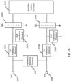
- FIG. 2A illustrates a block diagram of a capacitor coupling system that avoids use of external blocking capacitors.
- This is but one possible block diagram configuration and it is contemplated that other arrangement of elements are possible that do not depart from the claimed innovation or the scope of the improvement over the prior art.
- This is a differential pair configuration and as such the upper signal path is discussed in detail.
- the lower signal path is generally identical and symmetric to the upper path.
- two inputs Vin + 208A and Vin - 208B are shown to receive the incoming differential signal.
- Connected to each of the input terminals 208A, 208B are one or more impedance matching elements 212.
- these elements comprise one or more resistors and one or more capacitors. In other embodiments, other elements may be included or left out.
- the impedance matching element 212 is configured to match the input impedance of the driver amplifier 120 to the data source 104 providing the signals to the inputs Vin + 208A and Vin' 208B to avoid reflection and minimize return loss.
- the input impedance may be 50 ohms.
- the input impedance seen at Vin + 208A depends on the combination of the impedance matching elements 212 as well as the 1 st impedance element 216A and 2 nd impedance element 220A, and these three elements are tuned together to provide a desired through-response and input impedance.
- first impedance element 216A Also connected to input Vin + 208A is a first impedance element 216A.
- the output of the first impedance element 216A connects to a second impedance element 220A and a biasing element 224.
- the opposing terminal of the second impedance element 220A connects to ground.
- the first impedance element 216A and the second impedance element 220A form an impedance network, specifically a voltage divider or capacitor divider.
- the combination of the first impedance element 216A and the second impedance element 220A, both of which when combined as shown replace the large external blocking capacitor (also referred to as a coupling capacitor). Silicon is much more economical thus, integrating the blocking capacitor with the silicon driver lowers the total cost, as well as the size.
- the input signal presented to the input Vin + passes through the first capacitive element 216A toward the second capacitive element 220A. A portion of the input signal passes to ground through the second capacitive element 220A.
- the capacitors 216A appears as an open circuit to DC components of the input signal thereby blocking unwanted DC signal components from reaching and possibly disrupting the biasing element the amplifier section of the driver.
- Vout depends only on the ratio of capacitances and is therefore frequency independent, which mean that ideally this circuit work as low as DC (excluding exactly DC which is undefined).
- the actual size of the capacitor is not critical - the ratio of the capacitance is what matters.
- the capacitor divider topology as a ratio integrated on chip can achieve the same low frequency performance with a much smaller capacitance value.
- parasitics in the capacitors and the load on the output of the capacitive divider limit how low the capacitive divider works.
- modern semiconductor processes allow this network to work well below 1 MHz.
- the biasing element 224 connects to a supply voltage Vcc and a ground terminal to provide biasing to amplifier section 230 of the driver. Any DC signal components received on the input 208A, 208B can interfere with the biasing element output or vice versa interfere with data source 104. As a result, it is preferable to block DC components with the AC coupling capacitor (also referred to as a DC blocking capacitor). Biasing elements 224A, 224B are generally known and as such are not described in detail herein.
- the output of the biasing element 224A connects to an amplifier section 230 of the driver 120.
- the amplifier section 230 amplifies the signal to a level suitable for driving the optic modulator and optic signal generator, such as a laser or diode. Although shown as a single amplifier, it is contemplated that each path (upper path and lower path) may have a separate amplifier. The lower path is generally similar to the upper path and as such is not described in detail.
- FIG. 2B is a block diagram of an example embodiment of an integrated circuit located coupling capacitor arrangement for a single ended signal. As compared to Figure 2A , similar elements are labeled with identical reference numbers.
- This embodiment is a singled ended configuration and as such, a single input 208A is provided.
- the impedance matching elements 212 may comprise any combination of elements, active or passive, to match the input impedance of driver to a data source. In other embodiments, other single ended configurations are possible that also benefit from an integrated voltage divider network that blocks DC signal components to avoid use of external capacitors.
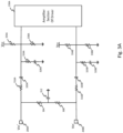
- Figure 3A illustrates one example embodiment of a circuit diagram of Figure 2A .
- the input Vin + 208A connects to a first impedance matching resistor 304 and resistor 316A.
- the opposing terminal of impedance matching resistor 304 connects to a second impedance matching resistor 308 and a capacitor 312.
- the opposing terminal of the second impedance matching resistor 308 connects to the lower signal path, which is configured generally similar to or identical to the upper signal path.
- the opposing terminal of resistor 316A connects in series with a capacitor 320A.
- the capacitor 320A opposing terminal connects to three different resistors, namely resistor 324A, and two resistors 334A, 338A of the biasing element.
- the opposing terminal of resistor 324A connects to capacitor 328A, which in turn connects to ground as shown.
- the resistor 316A and capacitor 320A form one impedance element of the DC block and the resistor 324A and capacitor 328A form the second impedance element of the DC block.
- Biasing resistor 334A of the biasing element also connects to a supply voltage node Vcc while biasing resistor 338A connects to a ground terminal as shown.
- An amplifier section 230 connects to the biasing resistors 334A, 338A and is configured to amplify a received signal.
- the resistors 304, 308 establish the low frequency input impedance. Resistors 304, 308 in conjunction with resistors 316A and 324A (and resistors 316B and 324B) establish the high frequency input impedance.
- the resistor 316A and capacitor 320A form a first capacitive element and the resistors 324A and capacitors 328A for a second capacitive element and operate as a capacitor divider network to block DC signal components while also passing the signal in the frequency band of interest, such as from 1MHz or lower (100 KHz) to 40 to 50 GHz or higher.
- capacitors 320A appears as an open circuit thereby preventing DC signal components from reaching the biasing elements and the capacitive element group 324A, 328A.
- the low frequency impedance looking into inputs 208A, 208B is determined by the resistors 304, 308, which in one embodiment is configured to be 100 ohms and in another embodiment to be 50 ohms.
- the capacitors 320A, 328A appear as short circuits thereby passing the input signal to the amplifier section 230.
- a voltage divider may occur in some embodiments but in other embodiment the full magnitude of the input signal is provided to the amplifier 230.
- the resistors 304, 308 are still part of the circuit for high frequency signals and establish part of the impedance matching.
- Z 208B R 308 II (R 316B + R 324 B).
- R 304 100 ⁇
- R 316A 50 ⁇
- R 324A 50 ⁇
- Figure 3B is a circuit level diagram of an example embodiment of an integrated circuit located coupling capacitor arrangement for a single ended signal. As compared to Figure 2A , similar elements are labeled with identical reference numbers.
- This embodiment is a singled ended configuration and as such, a single input 208A is provided.
- the impedance matching element 312 may comprise any combination of elements, active or passive, to match the input impedance of driver to a data source. In this embodiment the impedance matching element 312 is a capacitor.
- other single ended configurations are possible that also benefit from an integrated voltage divider network that blocks DC signal components to avoid use of external capacitors.
- Figure 4 illustrates a signal plot showing the performance of the embodiment of Figure 3A and 3B .
- the horizontal axis 404 represents frequency and the vertical axis 408 represents voltage ratios in dB.
- Signal line 412 represents the signal passing through the integrated circuit located coupling capacitors.
- the circuit has a good AC response at low frequencies, passing signals as low as 400kHz (-3dB cutoff) in this embodiment.
- this innovation achieves the goal of passing low frequency components in the frequency band of interest while blocking DC signal components at frequencies below the band of interest.
- the system serves as a successful signal block using the capacitive divider network described herein without the need for a large external blocking capacitor.
- Signal plot 416 represents the return loss of the capacitive structure and impedance matching features of the innovation shown in Figure 2A and 3A for differential signals/structure.
- Signal plot 420 represents the return loss of the capacitive structure and impedance matching features of the innovation shown in Figure 2B and 3B for singled ended signals/structure.
- a low return loss is preferred and is an indication of the quality of the impedance matching.
- the return loss S 11 is acceptable at low frequency, passing about 90% of the signal power and reflecting about 10% (reflection coefficient S11 is -10dB or 1/10 th of the incoming power) while being very low at higher frequencies.
- this innovative design also performs well from a return loss perspective.
Landscapes
- Engineering & Computer Science (AREA)
- Computer Networks & Wireless Communication (AREA)
- Signal Processing (AREA)
- Power Engineering (AREA)
- Physics & Mathematics (AREA)
- Electromagnetism (AREA)
- Amplifiers (AREA)
- Optical Communication System (AREA)
Description
- The invention relates to AC coupling topology, and in particular to an AC coupling arrangement located on an integrated circuit.
- Optical communication systems are commonly found in data centers and for long haul applications to transmit data at high data rates between two locations. Foundational to optical communication systems is the data to be transmitted, and a driver amplifier which amplifies a modulated signal onto an optical modulator. The interface between the data source and the driver must block DC signal components for preferred operation. This is typically achieved through use of an off-chip blocking capacitor.
-
Figure 1A illustrates a block diagram of an example environment of use, namely, an optic signal transmitter. This is but one possible environment of use and it is contemplated that other environments of use are possible. As shown inFigure 1A , adata source 104 supplies data for transmission over anoptic fiber 108. In one embodiment, the data source is a DSP. To achieve biasing of a driver, asupply voltage source 112 is provided to deliver power to the system. Thesupply voltage source 112 may be any source including a hard wire utility supplied power, power supply, battery, or any other source. Thesupply voltage source 112 provides a supply voltage to a bias circuit (part of the driver amplifier 120), which in turn provides a bias voltage to adriver amplifier 120. Thedriver amplifier 120 also receives the data to be transmitted in optic format from thedata source 104. Thedriver amplifier 120 includes one or more amplifiers configured to amplify and modulate the data to a level suitable for driving an optical modulator orlaser diode 124. Responsive to the signal from the driver, the optical modulator orlaser diode 124 generates theoptic signal 128, which is presented to the fiberoptic cable 108, for transmission to a remote location, such as for example another device in a data center or to a remote location in long haul applications. The frequency range of operation can be as high as several tens of Gigahertz (e.g. 50GHz) or higher and as low as 100 KHz. -
Figure 1B illustrates a block diagram of the interface between thedata source 104 and thedriver amplifier 120 that includes DC blocking capacitors. In this embodiment, there are four channels (C1, C2, C3, C4), and each channel is adifferential pair 170 comprising two conductive paths, namely apositive path 174 and anegative path 176. In series in each path is aDC blocking capacitor 182 as shown. Theblocking capacitors 182 function to block DC components from the signal passing from thedata source 104 to thedriver amplifier 120. In addition, the capacitance has to be large enough to allow the lowest frequency of operation in (e.g. 1 MHz or 100 KHz in various embodiments) without attenuating it. Furthermore, the capacitor needs to have low parasitics as to not influence the high frequency content. - Because of the aforementioned, blocking capacitors are typically external to the integrated circuit causing surface mount components to be used. As a drawback to the prior art, the blocking capacitors are large in size due to the requirement that the blocking capacitor block DC signal components yet the low pass frequency is 1 MHz. Due to the blocking capacitors being external to the integrated circuits which form the data source, the blocking capacitors are undesirably large in size. In some embodiments, the capacitor may be as large as the integrated circuit dedicated to the channel associated with the blocking capacitors. Because of the size of the blocking capacitors, the components have a large footprint consuming valuable real estate on the circuit board in contrast to technological trends which are towards smaller and more compact - not larger - configurations.
- Another downside to external blocking capacitors is that high fidelity surface mount components with good frequency performance carries a premium in cost. With the differential inputs and four channels shown in
Figure 1B , eight capacitors are needed. Example sizes for these blocking capacitors are 100 nano-farad capacitance and costs range between one to two dollars each, or up to sixteen dollars for all four channels. This further increases the space requirements and increases cost which is then passed onto the customers and/or reduces profit. Another drawback is that these capacitors add to customers and/or reduces profit. Another drawback is that these capacitors add to manufacture costs and can increase the failure rate due to the additional components. Any component outside of the integrated circuit requires transitions, transmission lines to connect to the component, and an assembly process leading to more parasitics, degraded performance, and increases assembly complexity. - The United States Patent Application Publication
US 2016/0173299 discloses an apparatus which comprises an amplifier and a passive continuous-time linear equalizer integrated with a baseline wander (BLW) corrector, wherein the integrated equalizer and BLW corrector is coupled to the amplifier. - To overcome the drawbacks of the prior art and provide additional benefits, a capacitive coupling system is disclosed. The present invention is defined by the appended independent claims. Specific embodiments are defined in the dependent claims. In one embodiment the system is configured as part of an integrated circuit to block DC components from an amplifier comprising. The system includes an input configured to receive an input signal such that the input signal has a DC component. A voltage divider network which has an input, an output, at least one resistor and at least one capacitor is also provided. The input is configured to receive the signal having a DC component such that the voltage divider network blocks the DC component. An amplifier is provided which has an input connected to the output of the voltage divider network.
- In one configuration, the voltage divider network comprises a first impedance element and a second impedance element. As such, the first impedance element and the second impedance element may comprise a resistor in series with a capacitor. In one embodiment, the amplifier includes a biasing element and the biasing element is configured to receive the input signal without the DC component. The biasing element includes a first resistor connected to a supply voltage and a second resistor connect to ground.
- The capacitive coupling system may be configured for differential signals and the system thus far described is associated with a positive path. The system may further comprise a negative path input configured to receive a negative path signal which has a DC component connected. This system also includes a negative path first impedance element having an input and an output. The input is configured to receive the negative path signal having a DC component such that the negative path first impedance element blocks the DC component. The negative path also includes a second impedance element configured to connect between the output of the negative path first impedance matching element and a ground node. The negative path second impedance element, when combined with the negative path first impedance element, forms a voltage divider network. An impedance matching element is provided and connected between the input of the positive path and the negative path input. The impedance matching element is configured to match an input impedance of the amplifier to a data source. The impedance matching element may be formed from one or more resistor connected in series between the input of the positive path and the negative path input and a capacitor connected to ground.
- Also disclosed herein is a capacitive coupling system configured as part of an integrated circuit for a differential pair to couple differential inputs to an amplifier. In one embodiment, the system comprises a positive path and a negative path. The positive path includes an input configured to receive a positive path input signal such that the positive path input signal has a DC component. Also part of the positive path is a first impedance element having an input and an output, the input is configured to receive the positive path input signal such that the first impedance element blocks the DC component. Also part of the positive path is a second impedance element configured to connect between the output of the first impedance matching element and a ground. The second impedance element, when combined with the first impedance element, forms a voltage divider network. An amplifier is provided which has an input connected to the output of the positive path first impedance element. The negative path includes an input configured to receive a negative path input signal which has a DC component. Also part of the negative path is a first impedance element having an input and an output. The input is configured to receive the negative path input signal such that the first impedance element blocks the DC component. A second impedance element is also provided and configured to connect between the output of the first impedance matching element and ground. The second impedance element when combined with the first impedance element forms a voltage divider network. The amplifier has an input connected to the output of the negative path first impedance element. Also part of this system is an impedance matching element connected between the positive path input and the negative path input. The impedance matching element configured to match an input impedance of the amplifier to a data source.
- In one embodiment, the positive path first impedance element comprises at least resistor and at least one capacitor. It is contemplated that the at least one resistor and the at least one capacitor are in series. In one configuration, the positive path second impedance element comprises at least resistor and at least one capacitor. The positive path second impedance element at least one resistor and the at least one capacitor may be in series and connect to a ground node.
- It is contemplated that the impedance matching element may comprise at least one resistor and at least one capacitor such that the capacitor is connected to ground. In this embodiment, the at least one resistor comprises two resistors connected in series between the positive path input and the negative path input forming a middle node between the two resistors and the capacitor connects to the middle node and to ground.
- Also disclosed is a method for coupling an input signal, connected a data source, to a driver and blocking DC components of an input signal. This method includes receiving the input signal from a data source such that the input signal has a DC component. This method also provides the input signal to a first impedance element. The first impedance element is configured as part of an integrated circuit. Next, blocking the DC component of the input signal with the first impedance element and then providing an output from the first impedance element to a second impedance element. The second impedance element configured as part of the integrated circuit. This method also establishes the input impedance with the second impedance element and the first impedance element to create an impedance matched signal, and then provides the impedance matched signal to the driver.
- In one embodiment, the input signal is a differential signal pair comprising a first signal on a first path and a second signal on a second path, the second path generally identical to the first path. The first and second path each have the first impedance element and the second impedance element and this embodiment further comprises matching the input impedance of the driver to the data course with an impedance matching element connected between the first path and the second path.
- In one configuration, the first impedance element and the second impedance element each comprise at least one resistor and at least one capacitor. It is contemplated that the impedance matching element may comprises an interconnect between the first path and the second path, the interconnect having two or more resistor in series and a capacitor connect ground from the interconnect to ground. In one embodiment, this method does not include blocking DC components with a capacitor, external to the integrated circuit, located between the data course and the driver. This method may further comprise biasing the driver with a biasing element such that the DC components are blocked from the biasing element by the first impedance element.
- Other systems, methods, features and advantages of the invention will be or will become apparent to one with skill in the art upon examination of the following figures and detailed description. It is intended that all such additional systems, methods, features and advantages be included within this description, be within the scope of the invention, and be protected by the accompanying claims.
- The components in the figures are not necessarily to scale, emphasis instead being placed upon illustrating the principles of the invention. In the figures, like reference numerals designate corresponding parts throughout the different views.
-
Figure 1A is a block diagram illustrating an example environment of use of the innovation disclosed herein. -
Figure 1B is a block diagram showing the coupling capacitors. -
Figure 2A is a block diagram of an example embodiment of an integrated circuit located coupling capacitor arrangement for a differential signal. -
Figure 2B is a block diagram of an example embodiment of an integrated circuit located coupling capacitor arrangement for a single ended signal. -
Figure 3A is a circuit diagram of an integrated circuit located coupling capacitor arrangement for a differential signal. -
Figure 3B is a circuit diagram of an integrated circuit located coupling capacitor arrangement for a single ended signal. -
Figure 4 illustrates signal plots of a signal and return loss. -
Figure 2A illustrates a block diagram of a capacitor coupling system that avoids use of external blocking capacitors. This is but one possible block diagram configuration and it is contemplated that other arrangement of elements are possible that do not depart from the claimed innovation or the scope of the improvement over the prior art. This is a differential pair configuration and as such the upper signal path is discussed in detail. The lower signal path is generally identical and symmetric to the upper path. As shown, twoinputs Vin + 208A andVin - 208B are shown to receive the incoming differential signal. Connected to each of theinput terminals driver amplifier 120 to thedata source 104 providing the signals to theinputs Vin + 208A and Vin' 208B to avoid reflection and minimize return loss. In some embodiments the input impedance may be 50 ohms. The input impedance seen atVin + 208A depends on the combination of the impedance matching elements 212 as well as the 1stimpedance element impedance element 220A, and these three elements are tuned together to provide a desired through-response and input impedance. - Also connected to input
Vin + 208A is afirst impedance element 216A. The output of thefirst impedance element 216A connects to asecond impedance element 220A and a biasing element 224. The opposing terminal of thesecond impedance element 220A connects to ground. Thefirst impedance element 216A and thesecond impedance element 220A form an impedance network, specifically a voltage divider or capacitor divider. The combination of thefirst impedance element 216A and thesecond impedance element 220A, both of which when combined as shown replace the large external blocking capacitor (also referred to as a coupling capacitor). Silicon is much more economical thus, integrating the blocking capacitor with the silicon driver lowers the total cost, as well as the size. - The input signal presented to the input Vin+ passes through the first
capacitive element 216A toward the secondcapacitive element 220A. A portion of the input signal passes to ground through the secondcapacitive element 220A. Thecapacitors 216A appears as an open circuit to DC components of the input signal thereby blocking unwanted DC signal components from reaching and possibly disrupting the biasing element the amplifier section of the driver. Thecapacitor divider network first impedance element 216A as Z1 and thesecond impedance element 220A as Z2, the following equation defines the output of the capacitance divider network: Vout = Z2/(Z1+Z2). When Z1=Z2, this equation can reduce to Z2/2Z2 which can be further reduced to ½. Fundamental to this invention is the idea of a capacitive divider, which in its ideal form works at all frequencies except for exactly DC. The math behind a capacitive divider shows that the impedance of a capacitor across frequency is Z = -j/[2*π*f*C]. Therefore the above example could be written as
sub 1 MHz operation, the capacitor divider topology as a ratio integrated on chip can achieve the same low frequency performance with a much smaller capacitance value. In practice, parasitics in the capacitors and the load on the output of the capacitive divider limit how low the capacitive divider works. However, modern semiconductor processes allow this network to work well below 1 MHz. - The biasing element 224 connects to a supply voltage Vcc and a ground terminal to provide biasing to
amplifier section 230 of the driver. Any DC signal components received on theinput data source 104. As a result, it is preferable to block DC components with the AC coupling capacitor (also referred to as a DC blocking capacitor).Biasing elements element 224A connects to anamplifier section 230 of thedriver 120. Theamplifier section 230 amplifies the signal to a level suitable for driving the optic modulator and optic signal generator, such as a laser or diode. Although shown as a single amplifier, it is contemplated that each path (upper path and lower path) may have a separate amplifier. The lower path is generally similar to the upper path and as such is not described in detail. -
Figure 2B is a block diagram of an example embodiment of an integrated circuit located coupling capacitor arrangement for a single ended signal. As compared toFigure 2A , similar elements are labeled with identical reference numbers. This embodiment is a singled ended configuration and as such, asingle input 208A is provided. The impedance matching elements 212 may comprise any combination of elements, active or passive, to match the input impedance of driver to a data source. In other embodiments, other single ended configurations are possible that also benefit from an integrated voltage divider network that blocks DC signal components to avoid use of external capacitors. -
Figure 3A illustrates one example embodiment of a circuit diagram ofFigure 2A . This is but one possible circuit level configuration and it is contemplated that other embodiments and configurations are possible that do not depart from the scope of the invention. In this embodiment, theinput Vin + 208A connects to a firstimpedance matching resistor 304 andresistor 316A. The opposing terminal ofimpedance matching resistor 304 connects to a secondimpedance matching resistor 308 and acapacitor 312. The opposing terminal of the secondimpedance matching resistor 308 connects to the lower signal path, which is configured generally similar to or identical to the upper signal path. - The opposing terminal of
resistor 316A connects in series with acapacitor 320A. Thecapacitor 320A opposing terminal connects to three different resistors, namelyresistor 324A, and tworesistors resistor 324A connects to capacitor 328A, which in turn connects to ground as shown. Theresistor 316A andcapacitor 320A form one impedance element of the DC block and theresistor 324A andcapacitor 328A form the second impedance element of the DC block. -
Biasing resistor 334A of the biasing element also connects to a supply voltage node Vcc while biasingresistor 338A connects to a ground terminal as shown. Anamplifier section 230 connects to the biasingresistors - The
resistors Resistors resistors resistors resistor 316A andcapacitor 320A form a first capacitive element and theresistors 324A andcapacitors 328A for a second capacitive element and operate as a capacitor divider network to block DC signal components while also passing the signal in the frequency band of interest, such as from 1MHz or lower (100 KHz) to 40 to 50 GHz or higher. - In response to DC or low frequency signal,
capacitors 320A appears as an open circuit thereby preventing DC signal components from reaching the biasing elements and thecapacitive element group inputs resistors capacitors amplifier section 230. A voltage divider may occur in some embodiments but in other embodiment the full magnitude of the input signal is provided to theamplifier 230. This voltage divider may increase linearity and thus in certain embodiments this is a further benefit of the present innovation based on this additional flexibility. Theresistors input leg 208A appears as theresistor 304 in parallel withresistor 316A in series withresistor 324A, or Z208A = R304II (R316A + R324A). A similar relationship holds forinput 208B andresistors -
Figure 3B is a circuit level diagram of an example embodiment of an integrated circuit located coupling capacitor arrangement for a single ended signal. As compared toFigure 2A , similar elements are labeled with identical reference numbers. This embodiment is a singled ended configuration and as such, asingle input 208A is provided. Theimpedance matching element 312 may comprise any combination of elements, active or passive, to match the input impedance of driver to a data source. In this embodiment theimpedance matching element 312 is a capacitor. In other embodiments, other single ended configurations are possible that also benefit from an integrated voltage divider network that blocks DC signal components to avoid use of external capacitors. -
Figure 4 illustrates a signal plot showing the performance of the embodiment ofFigure 3A and3B . In this plot thehorizontal axis 404 represents frequency and thevertical axis 408 represents voltage ratios in dB.Signal line 412 represents the signal passing through the integrated circuit located coupling capacitors. As can be seen, the circuit has a good AC response at low frequencies, passing signals as low as 400kHz (-3dB cutoff) in this embodiment. Thus, this innovation achieves the goal of passing low frequency components in the frequency band of interest while blocking DC signal components at frequencies below the band of interest. Thus, the system serves as a successful signal block using the capacitive divider network described herein without the need for a large external blocking capacitor.Signal plot 416 represents the return loss of the capacitive structure and impedance matching features of the innovation shown inFigure 2A and3A for differential signals/structure.Signal plot 420 represents the return loss of the capacitive structure and impedance matching features of the innovation shown inFigure 2B and3B for singled ended signals/structure. - A low return loss is preferred and is an indication of the quality of the impedance matching. As can be seen, the
return loss S 11 is acceptable at low frequency, passing about 90% of the signal power and reflecting about 10% (reflection coefficient S11 is -10dB or 1/10th of the incoming power) while being very low at higher frequencies. Thus, this innovative design also performs well from a return loss perspective. - Other systems, methods, features and advantages of the invention will be or will become apparent to one with skill in the art upon examination of the following figures and detailed description. It is intended that all such additional systems, methods, features and advantages be included within this description, be within the scope of the invention, and be protected by the accompanying claims.
- While various embodiments of the invention have been described, it will be apparent to those of ordinary skill in the art that many more embodiments and implementations are possible that are within the scope of this invention. In addition, the various features, elements, and embodiments described herein may be claimed or combined in any combination or arrangement.
Claims (13)
- A capacitive coupling system configured as part of an integrated circuit to block DC components from an amplifier comprising:an input (208A) configured to receive an input signal, the input signal having a DC component;a voltage divider network having an input, an output, at least one resistor and at least one capacitor, the input configured to receive the signal having a DC component such that the voltage divider network blocks the DC component and an amplifier having an input connected to the output of the voltage divider network wherein the voltage divider network comprises a first impedance element (216A) and a second impedance element (220A), the first impedance element (216A) having an input and an output, the input configured to receive the input signal such that the first impedance element blocks the DC component, and the second impedance element (220A) configured to connect between the output of the first impedance element and ground,characterized in that the first impedance element (216A) and the second impedance element (220A) (220A) each comprise a resistor (316A,324A)) in series with a capacitor (320A,324A); and the system further comprising an impedance matching element (212) connected between the input and ground, the impedance matching element (212) configured to match an input impedance of the amplifier to a data source, wherein the impedance matching element (212) comprises at least one capacitor (312) connected between the input and ground.
- The system of claim 1 wherein the amplifier includes a biasing element (224A), the biasing element (224A) configured to receive the input signal without the DC component.
- The system of claim 2 wherein the biasing element(224A) includes a first resistor (334A) connected to a supply voltage and a second resistor (338A, 338B) connect to ground.
- A capacitive coupling system configured as part of an integrated circuit for a differential pair to couple differential inputs to an amplifier, the system comprising:a positive path comprising:a positive path input (208A) configured to receive a positive path input signal, the positive path input signal having a DC component;a positive path first impedance element (216A) having an input and an output, the input configured to receive the positive path input signal such that the positive path first impedance element (216A) blocks the DC component;a positive path second impedance element (220A) configured to connect between the output of the positive path first impedance element (216A) and ground, the positive path second impedance element (220A) when combined with the positive path first impedance element form (216A) a voltage divider network;an amplifier having an input connected to the output of the positive path first impedance element.a negative path comprising:an input (208B) configured to receive a negative path input signal, the negative path input signal having a DC component;a negative path first impedance element (216B) having an input and an output, the input configured to receive the negative path input signal such that the negative path first impedance element (216B) blocks the DC component;a negative path second impedance element (220B) configured to connect between the output of the negative path first impedance element (216B) and ground, the negative path second impedance element (220B) when combined with the negative path first impedance element (216B) form a voltage divider network;the amplifier having an input connected to the output of the negative path first impedance element; and characterized byan impedance matching element (212) connected between the positive path input (208A) and the negative path input (208B), the impedance matching element (212) configured to match an input impedance of the amplifier to a data source, wherein the impedance matching element (212) comprises at least one resistor (304, 308), connected between the positive path and the negative path, and at least one capacitor (312) such that the at least one capacitor (312) is connected to ground.
- The system of claim 4
wherein the positive path first impedance element (216A) comprises at least resistor (316A) and at least one capacitor (320A). - The system of claim 5
wherein at least one resistor (316A) and the at least one capacitor (320A) are in series. - The system of claim 4
wherein the positive path second impedance element comprises at least resistor (324A) and at least one capacitor (328A). - The system of claim 7
wherein at least one resistor (324A) and the at least one capacitor (328A) are in series and connect to a ground node. - The system of claim 6
wherein the at least one resistor comprises two resistors (304, 308) connected in series between the positive path input and the negative path input forming a middle node between the two resistor and the capacitor (312) connects to the middle node and ground. - A method for coupling an input signal, connected a data source, to a driver and blocking DC components of an input signal comprising:receiving the input signal from a data source on a first path and a second path, the input signal having a DC component;providing the input signal to an impedance matching interconnect (212), wherein the impedance matching interconnect (212) interconnects between the first path and the second path, the interconnect having two or more resistors (304, 308) in series and a capacitor (312) connected from the interconnect (212) to the ground;providing the input signal to a first impedance element, the first impedance element configured as part of an integrated circuit;blocking the DC component of the input signal with the first impedance element (216A, 216B), such that the first impedance element (216A, 216B) is part of the integrated circuit;providing an output from the first impedance element (216A, 216B) to a second impedance element (220A, 220B), the second impedance element (220A, 220B) configured as part of the integrated circuit such that the second impedance element (220A, 220B) connects from the first impedance element (216A, 216B) to ground;establishing the input impedance with the impedance matching interconnect (212), the second impedance element (220A, 220B), and the first impedance element (216A, 216B), to create an impedance matched signal;providing the impedance matched signal to the driver wherein the input signal is a differential signal pair comprising a first signal on the first path and a second signal on the second path, the second path generally being identical to the first path, the first and second path each having the first impedance element (216A, 216B) and the second impedance element (220A, 220B), and further comprising matching the input impedance of the driver to the data source with the impedance matching element (212) connected between the first path and the second path.
- ++The method of claim 10
wherein the first impedance element (216A, 216B), and the second impedance element (220A, 220B) each comprise at least one resistor (316A, 316B; 324A, 324B) and at least one capacitor (320A, 320B ; 328A, 328B). - The method of claim 10
herein the method does not include blocking DC components with a capacitor, external to the integrated circuit, located between the data source and the driver. - The method of claim 10 further comprising biasing the driver with a biasing element (224A, 224B) such that the DC components are blocked from the biasing element.
Applications Claiming Priority (2)
| Application Number | Priority Date | Filing Date | Title |
|---|---|---|---|
| US201862678164P | 2018-05-30 | 2018-05-30 | |
| PCT/US2019/034730 WO2019232260A1 (en) | 2018-05-30 | 2019-05-30 | Integrated circuit based ac coupling topology |
Publications (3)
| Publication Number | Publication Date |
|---|---|
| EP3804247A1 EP3804247A1 (en) | 2021-04-14 |
| EP3804247A4 EP3804247A4 (en) | 2022-04-20 |
| EP3804247B1 true EP3804247B1 (en) | 2024-08-14 |
Family
ID=68697685
Family Applications (1)
| Application Number | Title | Priority Date | Filing Date |
|---|---|---|---|
| EP19811970.3A Active EP3804247B1 (en) | 2018-05-30 | 2019-05-30 | Integrated circuit based ac coupling topology |
Country Status (5)
| Country | Link |
|---|---|
| US (1) | US12184335B2 (en) |
| EP (1) | EP3804247B1 (en) |
| JP (1) | JP7653790B2 (en) |
| CN (1) | CN112352405B (en) |
| WO (1) | WO2019232260A1 (en) |
Families Citing this family (1)
| Publication number | Priority date | Publication date | Assignee | Title |
|---|---|---|---|---|
| US20250132745A1 (en) * | 2023-10-23 | 2025-04-24 | Lite-On Singapore Pte. Ltd. | Capacitive coupling isolation device and receiving circuit |
Family Cites Families (216)
| Publication number | Priority date | Publication date | Assignee | Title |
|---|---|---|---|---|
| US6570944B2 (en) | 2001-06-25 | 2003-05-27 | Rambus Inc. | Apparatus for data recovery in a synchronous chip-to-chip system |
| FR2495870A1 (en) | 1980-12-09 | 1982-06-11 | Thomson Csf | DEVICE FOR PROTECTING A LASER DIODE |
| US4545078A (en) | 1981-11-27 | 1985-10-01 | Siemens Aktiengesellschaft | Method and arrangement for controlling a light switch for optical signals |
| NL8200002A (en) | 1982-01-04 | 1983-08-01 | Philips Nv | ERROR LOCALIZATION DEVICE FOR DIGITAL OPTICAL TRANSMISSION SYSTEM. |
| JPS60260035A (en) | 1984-06-06 | 1985-12-23 | Fuji Photo Film Co Ltd | Residual image erasing method of cumulative phosphor sheet and its device |
| JP2575614B2 (en) | 1985-03-15 | 1997-01-29 | オリンパス光学工業株式会社 | Optical output stabilizer |
| US4747091A (en) | 1985-07-25 | 1988-05-24 | Olympus Optical Co., Ltd. | Semiconductor laser drive device |
| US4709416A (en) | 1986-02-24 | 1987-11-24 | Rca Corporation | Laser bias current stabilization for burst mode fiber optic communication system |
| JPH07112173B2 (en) | 1986-08-26 | 1995-11-29 | 日本電気株式会社 | Light modulation circuit |
| US5057932A (en) | 1988-12-27 | 1991-10-15 | Explore Technology, Inc. | Audio/video transceiver apparatus including compression means, random access storage means, and microwave transceiver means |
| US6023147A (en) | 1989-04-14 | 2000-02-08 | Intermec Ip Corp. | Hand held computerized data collection terminal with rechargeable battery pack sensor and battery power conservation |
| US6535187B1 (en) | 1998-04-21 | 2003-03-18 | Lawson A. Wood | Method for using a spatial light modulator |
| US5039194A (en) | 1990-01-09 | 1991-08-13 | International Business Machines Corporation | Optical fiber link card |
| US5625483A (en) | 1990-05-29 | 1997-04-29 | Symbol Technologies, Inc. | Integrated light source and scanning element implemented on a semiconductor or electro-optical substrate |
| US5019769A (en) | 1990-09-14 | 1991-05-28 | Finisar Corporation | Semiconductor laser diode controller and laser diode biasing control method |
| US6769792B1 (en) | 1991-04-30 | 2004-08-03 | Genlyte Thomas Group Llc | High intensity lighting projectors |
| JP2546080B2 (en) | 1991-05-10 | 1996-10-23 | 富士通株式会社 | Semiconductor laser control device |
| US5263026A (en) | 1991-06-27 | 1993-11-16 | Hughes Aircraft Company | Maximum likelihood sequence estimation based equalization within a mobile digital cellular receiver |
| JP2995971B2 (en) | 1991-11-27 | 1999-12-27 | 住友電気工業株式会社 | Semiconductor laser drive circuit |
| US5392273A (en) | 1992-02-28 | 1995-02-21 | Fujitsu Limited | Optical storage drive controller with predetermined light source drive values stored in non-volatile memory |
| WO1993021706A1 (en) | 1992-04-09 | 1993-10-28 | British Telecommunications Public Limited Company | Optical processing system |
| US5383046A (en) | 1992-05-29 | 1995-01-17 | Fujitsu Limited | Supervisory and control signal transmitting system for use in optically amplifying repeaters system |
| US5278404A (en) | 1992-07-20 | 1994-01-11 | At&T Bell Laboratories | Optical sub-system utilizing an embedded micro-controller |
| FR2694423B1 (en) | 1992-07-30 | 1994-12-23 | France Telecom | Device for controlling the output power of laser diodes. |
| US5463345A (en) | 1993-01-07 | 1995-10-31 | Nec Corporation | Circuit for converting unipolar input to bipolar output |
| JP3231886B2 (en) | 1993-03-31 | 2001-11-26 | 能美防災株式会社 | Photoelectric fire detector |
| US5448629A (en) | 1993-10-14 | 1995-09-05 | At&T Corp. | Amplitude detection scheme for optical transmitter control |
| US5488627A (en) | 1993-11-29 | 1996-01-30 | Lexmark International, Inc. | Spread spectrum clock generator and associated method |
| US5510924A (en) | 1994-01-13 | 1996-04-23 | Olympus Optical Co., Ltd. | Voice information transfer system capable of easily performing voice information transfer using optical signal |
| US5491548A (en) | 1994-03-18 | 1996-02-13 | Tektronix, Inc. | Optical signal measurement instrument and wide dynamic range optical receiver for use therein |
| JPH0818414A (en) | 1994-04-26 | 1996-01-19 | Hitachi Ltd | Delay circuit for signal processing |
| US5394416A (en) | 1994-05-11 | 1995-02-28 | Alcatel Network Systems, Inc. | Laser modulation controller using additive and amplitude modulation control tones |
| JPH0897774A (en) | 1994-09-29 | 1996-04-12 | Fujitsu Ltd | Optical terminal equipment with self-monitoring function |
| US5532471A (en) | 1994-12-21 | 1996-07-02 | At&T Corp. | Optical transimpedance amplifier with high dynamic range |
| JP3442897B2 (en) | 1995-03-08 | 2003-09-02 | Kddi株式会社 | Range-based gain control optical amplifier, range-based optical amplifier gain control method, optical receiver and optical repeater |
| US5673282A (en) | 1995-07-28 | 1997-09-30 | Lucent Technologies Inc. | Method and apparatus for monitoring performance of a laser transmitter |
| US5594748A (en) | 1995-08-10 | 1997-01-14 | Telephone Information Systems, Inc. | Method and apparatus for predicting semiconductor laser failure |
| TW312063B (en) | 1995-08-31 | 1997-08-01 | Sony Co Ltd | |
| FI954809L (en) | 1995-10-09 | 1997-04-10 | Nokia Telecommunications Oy | Forwarding maintenance messages from the fiber amplifier |
| US6108113A (en) | 1995-12-29 | 2000-08-22 | Mci Communications Corporation | Method and system for transporting ancillary network data |
| US6010538A (en) | 1996-01-11 | 2000-01-04 | Luxtron Corporation | In situ technique for monitoring and controlling a process of chemical-mechanical-polishing via a radiative communication link |
| US5943152A (en) | 1996-02-23 | 1999-08-24 | Ciena Corporation | Laser wavelength control device |
| US5844928A (en) | 1996-02-27 | 1998-12-01 | Lucent Technologies, Inc. | Laser driver with temperature sensor on an integrated circuit |
| CA2172873C (en) | 1996-03-28 | 2002-03-12 | Kim Byron Roberts | Method of determining optical amplifier failures |
| JPH09321701A (en) | 1996-05-31 | 1997-12-12 | Fujitsu Ltd | Optical communication system and optical amplifier |
| US5953690A (en) | 1996-07-01 | 1999-09-14 | Pacific Fiberoptics, Inc. | Intelligent fiberoptic receivers and method of operating and manufacturing the same |
| US5812572A (en) | 1996-07-01 | 1998-09-22 | Pacific Fiberoptics, Inc. | Intelligent fiberoptic transmitters and methods of operating and manufacturing the same |
| DE19629279C1 (en) | 1996-07-19 | 1997-11-20 | Ldt Gmbh & Co | Video projection device for representing video images made from defined size image points |
| JPH1065627A (en) | 1996-08-20 | 1998-03-06 | Fujitsu Ltd | Optical transmitter, optical communication system and optical communication method |
| JPH1069661A (en) | 1996-08-27 | 1998-03-10 | Mitsumi Electric Co Ltd | Laser control circuit for writable optical disk drive |
| JPH1093170A (en) | 1996-09-10 | 1998-04-10 | Fuji Xerox Co Ltd | Laser diode drive circuit, semiconductor integrated circuit for driving laser diode, and image recorder |
| JPH10126351A (en) | 1996-10-18 | 1998-05-15 | Nec Corp | Light-receiving circuit |
| US5837995A (en) | 1996-11-25 | 1998-11-17 | Alan Y. Chow | Wavelength-controllable voltage-phase photodiode optoelectronic switch ("opsistor") |
| CA2193782C (en) | 1996-12-23 | 2001-06-12 | Kai Di Feng | Adaptive infrared communication apparatus |
| US5926303A (en) | 1997-07-29 | 1999-07-20 | Alcatel Usa Sourcing, L.P. | System and apparatus for optical fiber interface |
| US6160647A (en) | 1997-08-09 | 2000-12-12 | Stratos Lightwave, Inc. | Optoelectronic transmitter with improved control circuit and laser fault latching |
| US5956168A (en) | 1997-08-14 | 1999-09-21 | Finisar Corporation | Multi-protocol dual fiber link laser diode controller and method |
| US5978393A (en) | 1997-08-25 | 1999-11-02 | Digital Optics Corporation | Laser diode power output controller and method thereof |
| USH1881H (en) | 1998-02-19 | 2000-10-03 | Dsc/Celcore, Inc. | System and method for forming circuit connections within a telecommunications switching platform |
| JPH11135871A (en) | 1997-10-28 | 1999-05-21 | Nec Corp | Method for activating laser diode and circuit thereof |
| US6494370B1 (en) | 1997-12-11 | 2002-12-17 | Ceyx Technologies | Electro-optic system controller and method of operation |
| KR100241780B1 (en) | 1997-12-16 | 2000-02-01 | 윤종용 | Power saving apparatus for radio communication terminal |
| US6512617B1 (en) | 1998-02-03 | 2003-01-28 | Applied Micro Circuits Corporation | Methods and systems for control and calibration of VCSEL-based optical transceivers |
| US6049413A (en) | 1998-05-22 | 2000-04-11 | Ciena Corporation | Optical amplifier having first and second stages and an attenuator controlled based on the gains of the first and second stages |
| US6014241A (en) | 1998-06-25 | 2000-01-11 | Tacan Corporation | Method and apparatus for reducing non-linear characteristics of a signal modulator by cross-correlation |
| US6211742B1 (en) | 1998-11-04 | 2001-04-03 | Broadcom Corporation | Lock detector for phase locked loops |
| US6115113A (en) | 1998-12-02 | 2000-09-05 | Lockheed Martin Corporation | Method for increasing single-pulse range resolution |
| JP2000269898A (en) | 1999-03-19 | 2000-09-29 | Fujitsu Ltd | Optical transmission circuit |
| US6801555B1 (en) | 1999-04-26 | 2004-10-05 | Finisar Corporation | Lasing semiconductor optical amplifier with output power monitor and control |
| JP2000357951A (en) | 1999-06-15 | 2000-12-26 | Mitsubishi Electric Corp | Delay circuit, clock generation circuit, and phase synchronization circuit |
| JP2001024272A (en) | 1999-07-09 | 2001-01-26 | Asahi Optical Co Ltd | Semiconductor laser degradation judgment circuit |
| JP2001053377A (en) | 1999-08-06 | 2001-02-23 | Asahi Optical Co Ltd | Semiconductor laser driver |
| JP2001110185A (en) | 1999-10-07 | 2001-04-20 | Mitsubishi Electric Corp | Clock synchronous semiconductor memory device |
| JP3541750B2 (en) | 1999-10-15 | 2004-07-14 | 松下電器産業株式会社 | Optical receiving preamplifier |
| US6366373B1 (en) | 1999-11-24 | 2002-04-02 | Luxn, Inc. | Method of intrinsic continuous management data transmission in fiber optic communications |
| US6954410B2 (en) | 2000-01-20 | 2005-10-11 | Hitachi, Ltd. | Information recording and reproducing apparatus for updating the waveform of a laser based on position information |
| JP2001209358A (en) | 2000-01-26 | 2001-08-03 | Seiko Epson Corp | Unevenness correction of display image |
| US6771679B2 (en) | 2000-05-17 | 2004-08-03 | David Chalmers Schie | Apparatus and method for programmable control of laser diode modulation and operating point |
| JP2002016316A (en) | 2000-06-30 | 2002-01-18 | Sanyo Denki Co Ltd | Semiconductor light emitting device output compensation method and device |
| US6661940B2 (en) | 2000-07-21 | 2003-12-09 | Finisar Corporation | Apparatus and method for rebroadcasting signals in an optical backplane bus system |
| US6423963B1 (en) | 2000-07-26 | 2002-07-23 | Onetta, Inc. | Safety latch for Raman amplifiers |
| JP4671478B2 (en) | 2000-08-08 | 2011-04-20 | 富士通株式会社 | Wavelength multiplexing optical communication system and wavelength multiplexing optical communication method |
| WO2002037628A1 (en) | 2000-11-06 | 2002-05-10 | Vitesse Semiconductor Corporation | Method of high speed direct-modulation for common-cathode laser array |
| US6822987B2 (en) | 2000-11-22 | 2004-11-23 | Optical Communication Products, Inc. | High-speed laser array driver |
| US6473224B2 (en) | 2000-12-01 | 2002-10-29 | Alcatel | Configurable safety shutdown for an optical amplifier using non-volatile storage |
| US6934307B2 (en) | 2000-12-12 | 2005-08-23 | International Business Machines Corporation | Multichannel communications link receiver having parallel optical components |
| US6947456B2 (en) | 2000-12-12 | 2005-09-20 | Agilent Technologies, Inc. | Open-loop laser driver having an integrated digital controller |
| US20040197101A1 (en) | 2001-02-05 | 2004-10-07 | Sasser Gary D. | Optical transceiver module with host accessible on-board diagnostics |
| US7079775B2 (en) | 2001-02-05 | 2006-07-18 | Finisar Corporation | Integrated memory mapped controller circuit for fiber optics transceiver |
| US6707600B1 (en) | 2001-03-09 | 2004-03-16 | Finisar Corporation | Early warning failure detection for a lasing semiconductor optical amplifier |
| JP4628566B2 (en) | 2001-03-12 | 2011-02-09 | 三菱電機株式会社 | Image projection device |
| US6593810B2 (en) | 2001-03-16 | 2003-07-15 | Intel Corporation | 2.5 Gigabits-per-second transimpedance amplifier |
| US7046721B2 (en) | 2001-03-20 | 2006-05-16 | Ericsson Inc. | System and method to enhance the capacity of a communication link |
| WO2003096759A1 (en) | 2001-03-30 | 2003-11-20 | Santur Corporation | High speed modulation of arrayed lasers |
| US6538394B2 (en) | 2001-03-30 | 2003-03-25 | Maxim Integrated Products, Inc. | Current source methods and apparatus for light emitting diodes |
| JP2004531948A (en) | 2001-04-30 | 2004-10-14 | ピレリー・サブマリン・テレコム・システムズ・イタリア・ソチエタ・ペル・アツィオーニ | Optical transmission system with monitoring system |
| US6657488B1 (en) | 2001-07-03 | 2003-12-02 | Silicon Laboratories, Inc. | Offset correction and slicing level adjustment for amplifier circuits |
| US6753931B2 (en) | 2001-08-10 | 2004-06-22 | Lightwave Electronics | Pulse sequencing for generating a color image in laser-based display systems |
| EP1289081A1 (en) | 2001-09-03 | 2003-03-05 | Agilent Technologies, Inc. (a Delaware corporation) | Laser driver circuit and method of driving a laser therewith |
| US6868104B2 (en) | 2001-09-06 | 2005-03-15 | Finisar Corporation | Compact laser package with integrated temperature control |
| EP1294189A3 (en) | 2001-09-18 | 2004-01-14 | Sony Corporation | Optical state modulation |
| US6533603B1 (en) | 2001-10-04 | 2003-03-18 | Finisar Corporation | Electronic module having an integrated latching mechanism |
| US7058315B2 (en) | 2001-10-09 | 2006-06-06 | Chiaro Networks Ltd. | Fast decision threshold controller for burst-mode receiver |
| US6738401B2 (en) | 2001-10-11 | 2004-05-18 | Quantum Bridge Communications, Inc. | High speed switching driver |
| US7049759B2 (en) | 2001-12-06 | 2006-05-23 | Linear Technology Corporation | Circuitry and methods for improving the performance of a light emitting element |
| KR100445910B1 (en) | 2001-12-27 | 2004-08-25 | 한국전자통신연구원 | Optical signal receiving apparatus and method having suitable receiving performance in spite of change of intensity of the optical signal |
| US6947455B2 (en) | 2002-02-12 | 2005-09-20 | Finisar Corporation | Maintaining desirable performance of optical emitters at extreme temperatures |
| US20050185149A1 (en) | 2002-03-28 | 2005-08-25 | Corporate Patent Counsel Phillips Electronics North America Corporation | Image projector with light source modulation according to image signal |
| JP3778119B2 (en) | 2002-04-01 | 2006-05-24 | 日本電気株式会社 | Power control apparatus and method for optical disk recording |
| US6740864B1 (en) | 2002-04-30 | 2004-05-25 | Finisar Corporation | Method and apparatus for monitoring optical switches and cross-connects |
| JP2004015409A (en) | 2002-06-06 | 2004-01-15 | Renesas Technology Corp | Semiconductor integrated circuit for communication and wireless communication system |
| JP2004022744A (en) | 2002-06-14 | 2004-01-22 | Sumitomo Electric Ind Ltd | Laser light generation unit control circuit and laser light generation unit control method |
| US6837625B2 (en) | 2002-06-24 | 2005-01-04 | Finisar Corporation | Flexible seal to reduce optical component contamination |
| US6954415B2 (en) | 2002-07-03 | 2005-10-11 | Ricoh Company, Ltd. | Light source drive, optical information recording apparatus, and optical information recording method |
| US7031574B2 (en) | 2002-07-10 | 2006-04-18 | Finisar Corporation | Plug-in module for providing bi-directional data transmission |
| US6941080B2 (en) * | 2002-07-15 | 2005-09-06 | Triquint Technology Holding Co. | Method and apparatus for directly modulating a laser diode using multi-stage driver circuitry |
| JP4085723B2 (en) | 2002-07-15 | 2008-05-14 | カシオ計算機株式会社 | Projection display device and display driving method thereof |
| US6852966B1 (en) | 2002-09-27 | 2005-02-08 | Finisar Corporation | Method and apparatus for compensating a photo-detector |
| US7016381B2 (en) | 2002-10-11 | 2006-03-21 | Ziva, Inc. | Current-controlled polarization switching vertical cavity surface emitting laser |
| US6956643B2 (en) | 2002-10-30 | 2005-10-18 | Finisar Corporation | Apparatus and method for testing optical transceivers |
| US7035300B2 (en) | 2002-11-05 | 2006-04-25 | Finisar Corporation | Calibration of a multi-channel optoelectronic module with integrated temperature control |
| US6828857B2 (en) | 2002-12-11 | 2004-12-07 | Intel Corporation | High gain, high bandwidth CMOS transimpedance amplifier |
| JP4060696B2 (en) | 2002-12-13 | 2008-03-12 | 日本オプネクスト株式会社 | Optical transmission module |
| US7206023B2 (en) | 2002-12-13 | 2007-04-17 | Belliveau Richard S | Image projection lighting devices with projection field light intensity uniformity adjustment |
| US7545839B2 (en) | 2003-01-02 | 2009-06-09 | Optiswitch Technology Corporation | Apparatus and method for driving a pulsed laser diode |
| US6836493B2 (en) | 2003-01-15 | 2004-12-28 | Agilent Technologies, Inc. | Laser initialization in firmware controlled optical transceiver |
| US6909731B2 (en) | 2003-01-23 | 2005-06-21 | Cheng Youn Lu | Statistic parameterized control loop for compensating power and extinction ratio of a laser diode |
| EP1445843B1 (en) | 2003-02-05 | 2006-09-20 | Alcatel | Driver and operation method for semiconductor lasers |
| US20040202215A1 (en) | 2003-04-09 | 2004-10-14 | Elantec Semiconductor, Inc. | Programmable damping for laser drivers |
| US6888123B2 (en) | 2003-05-09 | 2005-05-03 | Finisar Corporation | Method and apparatus for monitoring a photo-detector |
| US7009761B2 (en) | 2003-05-29 | 2006-03-07 | Fujitsu Limited | Power tilt compensation using automatic power balance control |
| US7215891B1 (en) | 2003-06-06 | 2007-05-08 | Jds Uniphase Corporation | Integrated driving, receiving, controlling, and monitoring for optical transceivers |
| KR100586225B1 (en) | 2003-06-16 | 2006-06-07 | 오연수 | Prefabricated membrane structures and methods for constructing membrane structures |
| US7003007B2 (en) | 2003-06-20 | 2006-02-21 | Maxim Integrated Products, Inc. | System and method for using an output transformer for packaged laser diode drivers |
| US7084704B2 (en) | 2003-07-31 | 2006-08-01 | Skyworks Solutions, Inc. | Variable gain amplifier system |
| GB2405295B (en) | 2003-08-19 | 2006-10-25 | Agilent Technologies Inc | Variable decision threshold apparatus |
| US6879217B2 (en) | 2003-09-05 | 2005-04-12 | Gennum Corporation | Triode region MOSFET current source to bias a transimpedance amplifier |
| US6864751B1 (en) | 2003-09-08 | 2005-03-08 | Texas Instruments Deutschland Gmbh | Transimpedance amplifier with adjustable output amplitude and wide input dynamic-range |
| US7184671B2 (en) | 2003-09-16 | 2007-02-27 | Opnext, Inc. | Optical transmission controller |
| US20080074562A1 (en) | 2003-11-01 | 2008-03-27 | Taro Endo | Display system comprising a mirror device with oscillation state |
| US7460585B2 (en) | 2003-11-04 | 2008-12-02 | Broadcom Corporation | Methods and systems for detecting defects in serial link transceivers |
| US20050105574A1 (en) | 2003-11-14 | 2005-05-19 | Wu Xin M. | Laser driver for optical communication network |
| US7127391B2 (en) | 2003-11-20 | 2006-10-24 | Mindspeed Technologies, Inc. | Method and apparatus for slice point determination |
| US7193151B2 (en) | 2004-03-12 | 2007-03-20 | Charles Industries, Ltd. | Electronic enclosure |
| JP4029852B2 (en) | 2004-03-23 | 2008-01-09 | セイコーエプソン株式会社 | Optical display device, optical display device control program, and optical display device control method |
| US7372882B2 (en) | 2004-04-28 | 2008-05-13 | Renesas Technology Corp. | Driving circuit for and semiconductor device for driving laser diode |
| WO2005115012A1 (en) | 2004-05-11 | 2005-12-01 | Thomson Licensing | System for using larger arc lamps with smaller imagers in a two-stage system comprising two imagers in series |
| WO2006002347A1 (en) * | 2004-06-23 | 2006-01-05 | Peregrine Semiconductor Corporation | Integrated rf front end |
| US7357513B2 (en) | 2004-07-30 | 2008-04-15 | Novalux, Inc. | System and method for driving semiconductor laser sources for displays |
| US7868701B2 (en) | 2004-08-03 | 2011-01-11 | Nippon Telephone And Telegraph Corporation | Transimpedance amplifier |
| US7719380B2 (en) * | 2004-08-17 | 2010-05-18 | Hewlett-Packard Development Company, L.P. | AC coupling circuit |
| US7005901B1 (en) | 2004-08-27 | 2006-02-28 | Mindspeed Technologies, Inc. | Process, temperature and supply insensitive trapezoidal pulse generator |
| US7265334B2 (en) | 2004-11-19 | 2007-09-04 | Mindspeed Technologies, Inc. | Laser power control with automatic compensation |
| US7504610B2 (en) | 2004-09-03 | 2009-03-17 | Mindspeed Technologies, Inc. | Optical modulation amplitude compensation system having a laser driver with modulation control signals |
| US7381935B2 (en) | 2004-11-19 | 2008-06-03 | Mindspeed Technologies, Inc. | Laser power control with automatic power compensation |
| US7276682B2 (en) | 2004-11-19 | 2007-10-02 | Mindspeed Technologies, Inc. | Laser power control with automatic compensation |
| US7375472B2 (en) | 2004-11-29 | 2008-05-20 | 02Micro International Limited | Highly efficient driving of photoflash diodes using low and fixed voltage drop-out current sink |
| US7301394B2 (en) | 2004-12-13 | 2007-11-27 | Broadcom Corporation | Impedance matched variable gain low noise amplifier using shunt feed-back |
| US7400662B2 (en) | 2005-01-26 | 2008-07-15 | Avago Technologies Fiber Ip Pte Ltd | Calibration of laser systems |
| JP2006267995A (en) | 2005-02-28 | 2006-10-05 | Yamaha Corp | Video reproducer of projection type |
| US7181100B2 (en) | 2005-03-09 | 2007-02-20 | Finisar Corporation | Interconnect mechanism for connecting a laser driver to a laser |
| US7321266B2 (en) | 2005-05-17 | 2008-01-22 | Integrated System Solution Corp. | Current-matching variable gain amplifier |
| US7450619B2 (en) | 2005-06-09 | 2008-11-11 | Mindspeed Technologies, Inc. | Laser driver loop control and method |
| US7418018B2 (en) | 2005-08-24 | 2008-08-26 | Sumitomo Electric Industries, Ltd. | Driver circuit for semiconductor laser diode |
| KR100771616B1 (en) | 2005-09-09 | 2007-10-31 | 엘지전자 주식회사 | Projection type display device and control method thereof |
| US7604357B2 (en) | 2005-10-11 | 2009-10-20 | Hewlett-Packard Development Company, L.P. | Adjusting light intensity |
| US20070085937A1 (en) | 2005-10-13 | 2007-04-19 | Boss Gregory J | Internal light masking in projection systems |
| JP4506640B2 (en) | 2005-10-19 | 2010-07-21 | 住友電気工業株式会社 | Semiconductor laser drive circuit |
| TWI325130B (en) | 2006-01-12 | 2010-05-21 | Himax Display Inc | Led current driving system for lcos display |
| US7853154B2 (en) | 2006-01-13 | 2010-12-14 | Mindspeed Technologies, Inc. | Bias circuit for burst-mode/TDM systems with power save feature |
| US7449948B2 (en) | 2006-01-30 | 2008-11-11 | Yamaha Corporation | Amplifier |
| JP4635892B2 (en) | 2006-02-09 | 2011-02-23 | セイコーエプソン株式会社 | Projection system, projector, image processing program, and recording medium on which image processing program is recorded |
| US7403064B2 (en) | 2006-03-16 | 2008-07-22 | Realtek Semiconductor Corp. | Dynamically accelerated operational amplifier and method thereof |
| JP2007281876A (en) | 2006-04-06 | 2007-10-25 | Nec Electronics Corp | Comparison circuit and its amplifying circuit |
| JP2007305762A (en) | 2006-05-11 | 2007-11-22 | Mitsubishi Electric Corp | Laser diode drive circuit |
| KR100705326B1 (en) | 2006-05-25 | 2007-04-10 | 삼성전자주식회사 | Feedback type variable gain amplifier and its control method |
| US7884557B2 (en) | 2006-07-14 | 2011-02-08 | Wolfson Microelectronics Plc | Protection circuit and method |
| US20080024469A1 (en) | 2006-07-31 | 2008-01-31 | Niranjan Damera-Venkata | Generating sub-frames for projection based on map values generated from at least one training image |
| JP4996294B2 (en) | 2007-03-19 | 2012-08-08 | 株式会社リコー | Power supply device, LED device using the power supply device, and electronic apparatus |
| US7701179B2 (en) | 2007-06-11 | 2010-04-20 | Faraday Technology Corp. | Control circuit and method for multi-mode buck-boost switching regulator |
| WO2008155384A1 (en) | 2007-06-19 | 2008-12-24 | Silicon Line Gmbh | Circuit arrangement and method for controlling light-emitting components |
| JP5095312B2 (en) | 2007-08-31 | 2012-12-12 | ラピスセミコンダクタ株式会社 | Class D amplifier circuit |
| US7701289B2 (en) | 2007-10-24 | 2010-04-20 | Industrial Technology Research Institute | Variable gain amplifier including series-coupled cascode amplifiers |
| US8094692B2 (en) | 2008-02-22 | 2012-01-10 | Nippon Telegraph And Telephone Corporation | Modulation method, modulation program, recording medium, modulation device, and optical transmitter |
| JP5035054B2 (en) | 2008-03-19 | 2012-09-26 | 住友電気工業株式会社 | Semiconductor laser drive circuit |
| US7768353B2 (en) | 2008-06-13 | 2010-08-03 | Samsung Electro-Mechanics Company, Ltd. | Systems and methods for switching mode power amplifier control |
| US8471496B2 (en) | 2008-09-05 | 2013-06-25 | Ketra, Inc. | LED calibration systems and related methods |
| US8148914B2 (en) | 2008-12-31 | 2012-04-03 | Texas Instruments Incorporated | Dynamic power saving pulse width modulated LED driver circuit |
| JP2010171062A (en) | 2009-01-20 | 2010-08-05 | Sumitomo Electric Ind Ltd | Optical transmitter |
| US8576928B2 (en) * | 2009-05-08 | 2013-11-05 | Intersil Americas Inc. | Capacitive divider transmission scheme for improved communications isolation |
| US8073030B2 (en) | 2009-07-23 | 2011-12-06 | Sumitomo Electric Industries, Ltd. | Shunt driver circuit for semiconductor laser diode |
| JP2011121545A (en) * | 2009-12-14 | 2011-06-23 | Denso Corp | On-vehicle control device |
| US8279019B2 (en) | 2010-05-10 | 2012-10-02 | Mediatek Singapore Pte. Ltd. | Millimeter-wave switches and attenuators |
| US8248164B2 (en) | 2010-09-02 | 2012-08-21 | Fairchild Semiconductor Corporation | Integrated circuit single ended-to-differential amplifier |
| US8461896B2 (en) | 2010-11-29 | 2013-06-11 | Advanced Micro Devices, Inc. | Compensating for wander in AC coupling data interface |
| US8319579B2 (en) * | 2010-11-29 | 2012-11-27 | Advanced Micro Devices, Inc. | Passive filter and AC coupler receiver interface |
| EP2512030A1 (en) | 2011-04-12 | 2012-10-17 | Nxp B.V. | Differential output stage |
| US8599966B2 (en) | 2011-06-30 | 2013-12-03 | International Business Machines Corporation | Coupling system for data receivers |
| JP5382375B2 (en) | 2011-08-31 | 2014-01-08 | 住友電気工業株式会社 | Drive circuit and home device |
| EP2568547B1 (en) | 2011-09-06 | 2014-04-16 | Leica Geosystems AG | Monitor diode-free laser driver |
| US8548336B2 (en) | 2011-12-02 | 2013-10-01 | Semtech Corporation | Closed loop optical modulation amplitude control |
| US8760131B2 (en) | 2012-01-06 | 2014-06-24 | Micrel, Inc. | High bandwidth PSRR power supply regulator |
| JP5337886B2 (en) | 2012-01-25 | 2013-11-06 | 株式会社フジクラ | DC coupled laser driving circuit and semiconductor laser element driving method |
| ITMI20120640A1 (en) * | 2012-04-18 | 2013-10-19 | St Microelectronics Srl | TRANS-IMPEDANCE AMPLIFIER FOR HIGH-SPEED OPTICAL-ELECTRIC INTERFACE |
| US20140063593A1 (en) | 2012-08-31 | 2014-03-06 | Martin Ole Berendt | Capacitor discharge pulse drive circuit with fast recovery |
| WO2014068351A2 (en) | 2012-10-31 | 2014-05-08 | Freescale Semiconductor, Inc. | Amplification stage and wideband power amplifier |
| US9287829B2 (en) | 2012-12-28 | 2016-03-15 | Peregrine Semiconductor Corporation | Control systems and methods for power amplifiers operating in envelope tracking mode |
| WO2015066867A1 (en) | 2013-11-07 | 2015-05-14 | Qualcomm Incorporated | Clock and data drivers with enhanced transconductance and suppressed output common-mode |
| JP6295778B2 (en) | 2014-03-28 | 2018-03-20 | 富士通株式会社 | Optical semiconductor device and drive circuit control method |
| US9491008B2 (en) | 2014-07-11 | 2016-11-08 | Rambus Inc. | On-chip AC coupled receiver with real-time linear baseline-wander compensation |
| US9602315B2 (en) * | 2014-12-12 | 2017-03-21 | Intel Corporation | Method and apparatus for passive continuous-time linear equalization with continuous-time baseline wander correction |
| US9306609B1 (en) * | 2015-01-13 | 2016-04-05 | Huawei Technologies Co., Ltd. | DC-coupled differential circuit front end |
| KR101690431B1 (en) | 2015-09-09 | 2016-12-27 | 숭실대학교산학협력단 | Amplifier with active balun |
| US10158211B2 (en) | 2015-09-22 | 2018-12-18 | Analog Devices, Inc. | Pulsed laser diode driver |
| US9780737B1 (en) | 2016-03-31 | 2017-10-03 | Avago Technologies General Ip (Singapore) Pte. Ltd. | Digitally-controlled transimpedance amplifier (TIA) circuit and methods |
| CN105897208B (en) | 2016-04-06 | 2019-10-25 | 江苏星宇芯联电子科技有限公司 | A kind of noninductive low-noise amplifier of high-gain automatic biasing |
-
2019
- 2019-05-30 WO PCT/US2019/034730 patent/WO2019232260A1/en not_active Ceased
- 2019-05-30 EP EP19811970.3A patent/EP3804247B1/en active Active
- 2019-05-30 CN CN201980042588.8A patent/CN112352405B/en active Active
- 2019-05-30 US US17/058,629 patent/US12184335B2/en active Active
- 2019-05-30 JP JP2020566795A patent/JP7653790B2/en active Active
Also Published As
| Publication number | Publication date |
|---|---|
| US12184335B2 (en) | 2024-12-31 |
| US20210211204A1 (en) | 2021-07-08 |
| JP7653790B2 (en) | 2025-03-31 |
| WO2019232260A1 (en) | 2019-12-05 |
| CN112352405B (en) | 2024-10-11 |
| JP2021525984A (en) | 2021-09-27 |
| EP3804247A1 (en) | 2021-04-14 |
| WO2019232260A8 (en) | 2021-01-14 |
| EP3804247A4 (en) | 2022-04-20 |
| CN112352405A (en) | 2021-02-09 |
Similar Documents
| Publication | Publication Date | Title |
|---|---|---|
| US6864750B2 (en) | Cascode distributed amplifier | |
| US6348837B1 (en) | Bi-directional amplifier having a single gain block for amplifying both forward and reverse signals | |
| JP5087773B2 (en) | Optical signal detection circuit and method | |
| US6943631B2 (en) | DC-coupled multi-stage amplifier using all-pass resistive/capacitive network for level shifting | |
| CN101986560B (en) | Amplifying circuit, semiconductor integrated circuit, wireless transmission system, and communication apparatus | |
| CA2069954C (en) | Fiber optic transimpedance receiver | |
| US20090091403A1 (en) | Contactless transmission of a differential signal between a transmitter and a receiver | |
| US20230283242A1 (en) | Amplifier device | |
| US12113483B2 (en) | DC coupled amplifier having pre-driver and bias control | |
| US6769133B1 (en) | Termination circuitry for dual forward and reverse test points for amplifiers | |
| US12184335B2 (en) | Integrated circuit based ac coupling topology | |
| US10897653B2 (en) | Power passing termination tap | |
| US8810333B2 (en) | Multiband coupling architecture | |
| US7221220B2 (en) | Method and apparatus for low-frequency bypass in broadband RF circuitry | |
| US20230244094A1 (en) | Optical communication device | |
| US20250192732A1 (en) | Integrated circuit ac coupling design with adjusted-ratio and high impedance emitter follower stage | |
| US7093276B2 (en) | CATV trunk amplifier, upward signal amplifier, and bi-directional CATV system | |
| US20240114109A1 (en) | Cable network device with low loss measurement port | |
| US6446263B1 (en) | Anti-loading CATV interface circuit and method | |
| US20040028313A1 (en) | Transmitter circuit comprising a light source and a communication system |
Legal Events
| Date | Code | Title | Description |
|---|---|---|---|
| STAA | Information on the status of an ep patent application or granted ep patent |
Free format text: STATUS: THE INTERNATIONAL PUBLICATION HAS BEEN MADE |
|
| PUAI | Public reference made under article 153(3) epc to a published international application that has entered the european phase |
Free format text: ORIGINAL CODE: 0009012 |
|
| STAA | Information on the status of an ep patent application or granted ep patent |
Free format text: STATUS: REQUEST FOR EXAMINATION WAS MADE |
|
| 17P | Request for examination filed |
Effective date: 20201210 |
|
| AK | Designated contracting states |
Kind code of ref document: A1 Designated state(s): AL AT BE BG CH CY CZ DE DK EE ES FI FR GB GR HR HU IE IS IT LI LT LU LV MC MK MT NL NO PL PT RO RS SE SI SK SM TR |
|
| AX | Request for extension of the european patent |
Extension state: BA ME |
|
| DAV | Request for validation of the european patent (deleted) | ||
| DAX | Request for extension of the european patent (deleted) | ||
| A4 | Supplementary search report drawn up and despatched |
Effective date: 20220323 |
|
| RIC1 | Information provided on ipc code assigned before grant |
Ipc: H04L 25/02 20060101AFI20220318BHEP |
|
| P01 | Opt-out of the competence of the unified patent court (upc) registered |
Effective date: 20230530 |
|
| GRAP | Despatch of communication of intention to grant a patent |
Free format text: ORIGINAL CODE: EPIDOSNIGR1 |
|
| STAA | Information on the status of an ep patent application or granted ep patent |
Free format text: STATUS: GRANT OF PATENT IS INTENDED |
|
| INTG | Intention to grant announced |
Effective date: 20240321 |
|
| GRAS | Grant fee paid |
Free format text: ORIGINAL CODE: EPIDOSNIGR3 |
|
| GRAA | (expected) grant |
Free format text: ORIGINAL CODE: 0009210 |
|
| STAA | Information on the status of an ep patent application or granted ep patent |
Free format text: STATUS: THE PATENT HAS BEEN GRANTED |
|
| AK | Designated contracting states |
Kind code of ref document: B1 Designated state(s): AL AT BE BG CH CY CZ DE DK EE ES FI FR GB GR HR HU IE IS IT LI LT LU LV MC MK MT NL NO PL PT RO RS SE SI SK SM TR |
|
| REG | Reference to a national code |
Ref country code: GB Ref legal event code: FG4D |
|
| REG | Reference to a national code |
Ref country code: CH Ref legal event code: EP |
|
| REG | Reference to a national code |
Ref country code: DE Ref legal event code: R096 Ref document number: 602019057087 Country of ref document: DE |
|
| REG | Reference to a national code |
Ref country code: IE Ref legal event code: FG4D |
|
| REG | Reference to a national code |
Ref country code: LT Ref legal event code: MG9D |
|
| REG | Reference to a national code |
Ref country code: NL Ref legal event code: MP Effective date: 20240814 |
|
| PG25 | Lapsed in a contracting state [announced via postgrant information from national office to epo] |
Ref country code: NO Free format text: LAPSE BECAUSE OF FAILURE TO SUBMIT A TRANSLATION OF THE DESCRIPTION OR TO PAY THE FEE WITHIN THE PRESCRIBED TIME-LIMIT Effective date: 20241114 |
|
| REG | Reference to a national code |
Ref country code: AT Ref legal event code: MK05 Ref document number: 1714291 Country of ref document: AT Kind code of ref document: T Effective date: 20240814 |
|
| PG25 | Lapsed in a contracting state [announced via postgrant information from national office to epo] |
Ref country code: NL Free format text: LAPSE BECAUSE OF FAILURE TO SUBMIT A TRANSLATION OF THE DESCRIPTION OR TO PAY THE FEE WITHIN THE PRESCRIBED TIME-LIMIT Effective date: 20240814 Ref country code: FI Free format text: LAPSE BECAUSE OF FAILURE TO SUBMIT A TRANSLATION OF THE DESCRIPTION OR TO PAY THE FEE WITHIN THE PRESCRIBED TIME-LIMIT Effective date: 20240814 Ref country code: PT Free format text: LAPSE BECAUSE OF FAILURE TO SUBMIT A TRANSLATION OF THE DESCRIPTION OR TO PAY THE FEE WITHIN THE PRESCRIBED TIME-LIMIT Effective date: 20241216 Ref country code: GR Free format text: LAPSE BECAUSE OF FAILURE TO SUBMIT A TRANSLATION OF THE DESCRIPTION OR TO PAY THE FEE WITHIN THE PRESCRIBED TIME-LIMIT Effective date: 20241115 Ref country code: PL Free format text: LAPSE BECAUSE OF FAILURE TO SUBMIT A TRANSLATION OF THE DESCRIPTION OR TO PAY THE FEE WITHIN THE PRESCRIBED TIME-LIMIT Effective date: 20240814 |
|
| PG25 | Lapsed in a contracting state [announced via postgrant information from national office to epo] |
Ref country code: BG Free format text: LAPSE BECAUSE OF FAILURE TO SUBMIT A TRANSLATION OF THE DESCRIPTION OR TO PAY THE FEE WITHIN THE PRESCRIBED TIME-LIMIT Effective date: 20240814 |
|
| PG25 | Lapsed in a contracting state [announced via postgrant information from national office to epo] |
Ref country code: LV Free format text: LAPSE BECAUSE OF FAILURE TO SUBMIT A TRANSLATION OF THE DESCRIPTION OR TO PAY THE FEE WITHIN THE PRESCRIBED TIME-LIMIT Effective date: 20240814 |
|
| PG25 | Lapsed in a contracting state [announced via postgrant information from national office to epo] |
Ref country code: AT Free format text: LAPSE BECAUSE OF FAILURE TO SUBMIT A TRANSLATION OF THE DESCRIPTION OR TO PAY THE FEE WITHIN THE PRESCRIBED TIME-LIMIT Effective date: 20240814 Ref country code: IS Free format text: LAPSE BECAUSE OF FAILURE TO SUBMIT A TRANSLATION OF THE DESCRIPTION OR TO PAY THE FEE WITHIN THE PRESCRIBED TIME-LIMIT Effective date: 20241214 |
|
| PG25 | Lapsed in a contracting state [announced via postgrant information from national office to epo] |
Ref country code: HR Free format text: LAPSE BECAUSE OF FAILURE TO SUBMIT A TRANSLATION OF THE DESCRIPTION OR TO PAY THE FEE WITHIN THE PRESCRIBED TIME-LIMIT Effective date: 20240814 |
|
| PG25 | Lapsed in a contracting state [announced via postgrant information from national office to epo] |
Ref country code: RS Free format text: LAPSE BECAUSE OF FAILURE TO SUBMIT A TRANSLATION OF THE DESCRIPTION OR TO PAY THE FEE WITHIN THE PRESCRIBED TIME-LIMIT Effective date: 20241114 Ref country code: ES Free format text: LAPSE BECAUSE OF FAILURE TO SUBMIT A TRANSLATION OF THE DESCRIPTION OR TO PAY THE FEE WITHIN THE PRESCRIBED TIME-LIMIT Effective date: 20240814 |
|
| PG25 | Lapsed in a contracting state [announced via postgrant information from national office to epo] |
Ref country code: RS Free format text: LAPSE BECAUSE OF FAILURE TO SUBMIT A TRANSLATION OF THE DESCRIPTION OR TO PAY THE FEE WITHIN THE PRESCRIBED TIME-LIMIT Effective date: 20241114 Ref country code: PT Free format text: LAPSE BECAUSE OF FAILURE TO SUBMIT A TRANSLATION OF THE DESCRIPTION OR TO PAY THE FEE WITHIN THE PRESCRIBED TIME-LIMIT Effective date: 20241216 Ref country code: PL Free format text: LAPSE BECAUSE OF FAILURE TO SUBMIT A TRANSLATION OF THE DESCRIPTION OR TO PAY THE FEE WITHIN THE PRESCRIBED TIME-LIMIT Effective date: 20240814 Ref country code: NO Free format text: LAPSE BECAUSE OF FAILURE TO SUBMIT A TRANSLATION OF THE DESCRIPTION OR TO PAY THE FEE WITHIN THE PRESCRIBED TIME-LIMIT Effective date: 20241114 Ref country code: NL Free format text: LAPSE BECAUSE OF FAILURE TO SUBMIT A TRANSLATION OF THE DESCRIPTION OR TO PAY THE FEE WITHIN THE PRESCRIBED TIME-LIMIT Effective date: 20240814 Ref country code: LV Free format text: LAPSE BECAUSE OF FAILURE TO SUBMIT A TRANSLATION OF THE DESCRIPTION OR TO PAY THE FEE WITHIN THE PRESCRIBED TIME-LIMIT Effective date: 20240814 Ref country code: IS Free format text: LAPSE BECAUSE OF FAILURE TO SUBMIT A TRANSLATION OF THE DESCRIPTION OR TO PAY THE FEE WITHIN THE PRESCRIBED TIME-LIMIT Effective date: 20241214 Ref country code: HR Free format text: LAPSE BECAUSE OF FAILURE TO SUBMIT A TRANSLATION OF THE DESCRIPTION OR TO PAY THE FEE WITHIN THE PRESCRIBED TIME-LIMIT Effective date: 20240814 Ref country code: GR Free format text: LAPSE BECAUSE OF FAILURE TO SUBMIT A TRANSLATION OF THE DESCRIPTION OR TO PAY THE FEE WITHIN THE PRESCRIBED TIME-LIMIT Effective date: 20241115 Ref country code: FI Free format text: LAPSE BECAUSE OF FAILURE TO SUBMIT A TRANSLATION OF THE DESCRIPTION OR TO PAY THE FEE WITHIN THE PRESCRIBED TIME-LIMIT Effective date: 20240814 Ref country code: ES Free format text: LAPSE BECAUSE OF FAILURE TO SUBMIT A TRANSLATION OF THE DESCRIPTION OR TO PAY THE FEE WITHIN THE PRESCRIBED TIME-LIMIT Effective date: 20240814 Ref country code: BG Free format text: LAPSE BECAUSE OF FAILURE TO SUBMIT A TRANSLATION OF THE DESCRIPTION OR TO PAY THE FEE WITHIN THE PRESCRIBED TIME-LIMIT Effective date: 20240814 Ref country code: AT Free format text: LAPSE BECAUSE OF FAILURE TO SUBMIT A TRANSLATION OF THE DESCRIPTION OR TO PAY THE FEE WITHIN THE PRESCRIBED TIME-LIMIT Effective date: 20240814 |
|
| PG25 | Lapsed in a contracting state [announced via postgrant information from national office to epo] |
Ref country code: SM Free format text: LAPSE BECAUSE OF FAILURE TO SUBMIT A TRANSLATION OF THE DESCRIPTION OR TO PAY THE FEE WITHIN THE PRESCRIBED TIME-LIMIT Effective date: 20240814 Ref country code: DK Free format text: LAPSE BECAUSE OF FAILURE TO SUBMIT A TRANSLATION OF THE DESCRIPTION OR TO PAY THE FEE WITHIN THE PRESCRIBED TIME-LIMIT Effective date: 20240814 Ref country code: RO Free format text: LAPSE BECAUSE OF FAILURE TO SUBMIT A TRANSLATION OF THE DESCRIPTION OR TO PAY THE FEE WITHIN THE PRESCRIBED TIME-LIMIT Effective date: 20240814 |
|
| PG25 | Lapsed in a contracting state [announced via postgrant information from national office to epo] |
Ref country code: EE Free format text: LAPSE BECAUSE OF FAILURE TO SUBMIT A TRANSLATION OF THE DESCRIPTION OR TO PAY THE FEE WITHIN THE PRESCRIBED TIME-LIMIT Effective date: 20240814 |
|
| PG25 | Lapsed in a contracting state [announced via postgrant information from national office to epo] |
Ref country code: CZ Free format text: LAPSE BECAUSE OF FAILURE TO SUBMIT A TRANSLATION OF THE DESCRIPTION OR TO PAY THE FEE WITHIN THE PRESCRIBED TIME-LIMIT Effective date: 20240814 |
|
| PG25 | Lapsed in a contracting state [announced via postgrant information from national office to epo] |
Ref country code: IT Free format text: LAPSE BECAUSE OF FAILURE TO SUBMIT A TRANSLATION OF THE DESCRIPTION OR TO PAY THE FEE WITHIN THE PRESCRIBED TIME-LIMIT Effective date: 20240814 Ref country code: SK Free format text: LAPSE BECAUSE OF FAILURE TO SUBMIT A TRANSLATION OF THE DESCRIPTION OR TO PAY THE FEE WITHIN THE PRESCRIBED TIME-LIMIT Effective date: 20240814 |
|
| REG | Reference to a national code |
Ref country code: DE Ref legal event code: R097 Ref document number: 602019057087 Country of ref document: DE |
|
| PLBE | No opposition filed within time limit |
Free format text: ORIGINAL CODE: 0009261 |
|
| STAA | Information on the status of an ep patent application or granted ep patent |
Free format text: STATUS: NO OPPOSITION FILED WITHIN TIME LIMIT |
|
| PGFP | Annual fee paid to national office [announced via postgrant information from national office to epo] |
Ref country code: DE Payment date: 20250528 Year of fee payment: 7 |
|
| PGFP | Annual fee paid to national office [announced via postgrant information from national office to epo] |
Ref country code: FR Payment date: 20250526 Year of fee payment: 7 |
|
| 26N | No opposition filed |
Effective date: 20250515 |
|
| PG25 | Lapsed in a contracting state [announced via postgrant information from national office to epo] |
Ref country code: SE Free format text: LAPSE BECAUSE OF FAILURE TO SUBMIT A TRANSLATION OF THE DESCRIPTION OR TO PAY THE FEE WITHIN THE PRESCRIBED TIME-LIMIT Effective date: 20240814 |
|
| REG | Reference to a national code |
Ref country code: CH Ref legal event code: H13 Free format text: ST27 STATUS EVENT CODE: U-0-0-H10-H13 (AS PROVIDED BY THE NATIONAL OFFICE) Effective date: 20251223 |
|
| PG25 | Lapsed in a contracting state [announced via postgrant information from national office to epo] |
Ref country code: LU Free format text: LAPSE BECAUSE OF NON-PAYMENT OF DUE FEES Effective date: 20250530 |
|
| PG25 | Lapsed in a contracting state [announced via postgrant information from national office to epo] |
Ref country code: CH Free format text: LAPSE BECAUSE OF NON-PAYMENT OF DUE FEES Effective date: 20250531 |
|
| GBPC | Gb: european patent ceased through non-payment of renewal fee |
Effective date: 20250530 |
|
| REG | Reference to a national code |
Ref country code: BE Ref legal event code: MM Effective date: 20250531 |
|
| PG25 | Lapsed in a contracting state [announced via postgrant information from national office to epo] |
Ref country code: MC Free format text: LAPSE BECAUSE OF FAILURE TO SUBMIT A TRANSLATION OF THE DESCRIPTION OR TO PAY THE FEE WITHIN THE PRESCRIBED TIME-LIMIT Effective date: 20240814 |
|
| PG25 | Lapsed in a contracting state [announced via postgrant information from national office to epo] |
Ref country code: GB Free format text: LAPSE BECAUSE OF NON-PAYMENT OF DUE FEES Effective date: 20250530 |
|
| PG25 | Lapsed in a contracting state [announced via postgrant information from national office to epo] |
Ref country code: IE Free format text: LAPSE BECAUSE OF NON-PAYMENT OF DUE FEES Effective date: 20250530 |
|
| PG25 | Lapsed in a contracting state [announced via postgrant information from national office to epo] |
Ref country code: BE Free format text: LAPSE BECAUSE OF NON-PAYMENT OF DUE FEES Effective date: 20250531 |