EP3802728B1 - Stabilized fluoride phosphor for light emitting diode (led) applications - Google Patents
Stabilized fluoride phosphor for light emitting diode (led) applications Download PDFInfo
- Publication number
- EP3802728B1 EP3802728B1 EP19731393.5A EP19731393A EP3802728B1 EP 3802728 B1 EP3802728 B1 EP 3802728B1 EP 19731393 A EP19731393 A EP 19731393A EP 3802728 B1 EP3802728 B1 EP 3802728B1
- Authority
- EP
- European Patent Office
- Prior art keywords
- phosphor
- particles
- reaction mixture
- fluoride phosphor
- inorganic coating
- Prior art date
- Legal status (The legal status is an assumption and is not a legal conclusion. Google has not performed a legal analysis and makes no representation as to the accuracy of the status listed.)
- Active
Links
Images




Classifications
-
- H—ELECTRICITY
- H10—SEMICONDUCTOR DEVICES; ELECTRIC SOLID-STATE DEVICES NOT OTHERWISE PROVIDED FOR
- H10H—INORGANIC LIGHT-EMITTING SEMICONDUCTOR DEVICES HAVING POTENTIAL BARRIERS
- H10H20/00—Individual inorganic light-emitting semiconductor devices having potential barriers, e.g. light-emitting diodes [LED]
- H10H20/80—Constructional details
- H10H20/85—Packages
- H10H20/851—Wavelength conversion means
- H10H20/8511—Wavelength conversion means characterised by their material, e.g. binder
- H10H20/8512—Wavelength conversion materials
-
- C—CHEMISTRY; METALLURGY
- C09—DYES; PAINTS; POLISHES; NATURAL RESINS; ADHESIVES; COMPOSITIONS NOT OTHERWISE PROVIDED FOR; APPLICATIONS OF MATERIALS NOT OTHERWISE PROVIDED FOR
- C09K—MATERIALS FOR MISCELLANEOUS APPLICATIONS, NOT PROVIDED FOR ELSEWHERE
- C09K11/00—Luminescent materials, e.g. electroluminescent or chemiluminescent
- C09K11/02—Use of particular materials as binders, particle coatings or suspension media therefor
- C09K11/025—Use of particular materials as binders, particle coatings or suspension media therefor non-luminescent particle coatings or suspension media
-
- C—CHEMISTRY; METALLURGY
- C09—DYES; PAINTS; POLISHES; NATURAL RESINS; ADHESIVES; COMPOSITIONS NOT OTHERWISE PROVIDED FOR; APPLICATIONS OF MATERIALS NOT OTHERWISE PROVIDED FOR
- C09K—MATERIALS FOR MISCELLANEOUS APPLICATIONS, NOT PROVIDED FOR ELSEWHERE
- C09K11/00—Luminescent materials, e.g. electroluminescent or chemiluminescent
- C09K11/08—Luminescent materials, e.g. electroluminescent or chemiluminescent containing inorganic luminescent materials
- C09K11/0827—Halogenides
- C09K11/0833—Halogenides with alkali or alkaline earth metals
-
- C—CHEMISTRY; METALLURGY
- C09—DYES; PAINTS; POLISHES; NATURAL RESINS; ADHESIVES; COMPOSITIONS NOT OTHERWISE PROVIDED FOR; APPLICATIONS OF MATERIALS NOT OTHERWISE PROVIDED FOR
- C09K—MATERIALS FOR MISCELLANEOUS APPLICATIONS, NOT PROVIDED FOR ELSEWHERE
- C09K11/00—Luminescent materials, e.g. electroluminescent or chemiluminescent
- C09K11/08—Luminescent materials, e.g. electroluminescent or chemiluminescent containing inorganic luminescent materials
- C09K11/55—Luminescent materials, e.g. electroluminescent or chemiluminescent containing inorganic luminescent materials containing beryllium, magnesium, alkali metals or alkaline earth metals
-
- C—CHEMISTRY; METALLURGY
- C09—DYES; PAINTS; POLISHES; NATURAL RESINS; ADHESIVES; COMPOSITIONS NOT OTHERWISE PROVIDED FOR; APPLICATIONS OF MATERIALS NOT OTHERWISE PROVIDED FOR
- C09K—MATERIALS FOR MISCELLANEOUS APPLICATIONS, NOT PROVIDED FOR ELSEWHERE
- C09K11/00—Luminescent materials, e.g. electroluminescent or chemiluminescent
- C09K11/08—Luminescent materials, e.g. electroluminescent or chemiluminescent containing inorganic luminescent materials
- C09K11/59—Luminescent materials, e.g. electroluminescent or chemiluminescent containing inorganic luminescent materials containing silicon
-
- C—CHEMISTRY; METALLURGY
- C09—DYES; PAINTS; POLISHES; NATURAL RESINS; ADHESIVES; COMPOSITIONS NOT OTHERWISE PROVIDED FOR; APPLICATIONS OF MATERIALS NOT OTHERWISE PROVIDED FOR
- C09K—MATERIALS FOR MISCELLANEOUS APPLICATIONS, NOT PROVIDED FOR ELSEWHERE
- C09K11/00—Luminescent materials, e.g. electroluminescent or chemiluminescent
- C09K11/08—Luminescent materials, e.g. electroluminescent or chemiluminescent containing inorganic luminescent materials
- C09K11/61—Luminescent materials, e.g. electroluminescent or chemiluminescent containing inorganic luminescent materials containing fluorine, chlorine, bromine, iodine or unspecified halogen elements
- C09K11/615—Halogenides
- C09K11/616—Halogenides with alkali or alkaline earth metals
-
- C—CHEMISTRY; METALLURGY
- C09—DYES; PAINTS; POLISHES; NATURAL RESINS; ADHESIVES; COMPOSITIONS NOT OTHERWISE PROVIDED FOR; APPLICATIONS OF MATERIALS NOT OTHERWISE PROVIDED FOR
- C09K—MATERIALS FOR MISCELLANEOUS APPLICATIONS, NOT PROVIDED FOR ELSEWHERE
- C09K11/00—Luminescent materials, e.g. electroluminescent or chemiluminescent
- C09K11/08—Luminescent materials, e.g. electroluminescent or chemiluminescent containing inorganic luminescent materials
- C09K11/61—Luminescent materials, e.g. electroluminescent or chemiluminescent containing inorganic luminescent materials containing fluorine, chlorine, bromine, iodine or unspecified halogen elements
- C09K11/617—Silicates
-
- H—ELECTRICITY
- H10—SEMICONDUCTOR DEVICES; ELECTRIC SOLID-STATE DEVICES NOT OTHERWISE PROVIDED FOR
- H10H—INORGANIC LIGHT-EMITTING SEMICONDUCTOR DEVICES HAVING POTENTIAL BARRIERS
- H10H20/00—Individual inorganic light-emitting semiconductor devices having potential barriers, e.g. light-emitting diodes [LED]
- H10H20/01—Manufacture or treatment
-
- H—ELECTRICITY
- H10—SEMICONDUCTOR DEVICES; ELECTRIC SOLID-STATE DEVICES NOT OTHERWISE PROVIDED FOR
- H10H—INORGANIC LIGHT-EMITTING SEMICONDUCTOR DEVICES HAVING POTENTIAL BARRIERS
- H10H20/00—Individual inorganic light-emitting semiconductor devices having potential barriers, e.g. light-emitting diodes [LED]
- H10H20/80—Constructional details
- H10H20/84—Coatings, e.g. passivation layers or antireflective coatings
Definitions
- the present disclosure is related generally to light emitting diodes (LEDs) and more specifically to coated fluoride phosphors for LED applications.
- Manganese-activated, red-emitting fluoride phosphors have recently emerged as an important class of LED down-converters due to their narrow-band spectral emission, high photoluminescence efficiency, and low thermal quenching. When incorporated into LED components, these phosphors can enhance the performance of both lighting and display products. Of this class of materials, manganese-activated potassium fluorosilicate (KSF:Mn) is the most notable, having become commercially available in the past few years.
- KSF:Mn manganese-activated potassium fluorosilicate
- KSF:Mn enables warm-white LED components with high luminous efficacy (Im/W) while preserving a high color rendering index (CRI), typically greater than 90.
- the phosphor's narrow red emission band results in less "wasted” light emitted into the far-red and infrared when compared to conventional phosphors.
- KSF:Mn enables a wider color gamut due to its saturated narrow band emission.
- WO2018005448A1 describes coated manganese doped phosphors.
- WO2018002556A1 describes a method for producing photoluminescent particles.
- a stabilized fluoride phosphor according to claim 1 there is provided a stabilized fluoride phosphor according to claim 1.
- a stabilized fluoride phosphor for light emitting diode applications includes particles comprising manganese-activated potassium fluorosilicate and an inorganic coating on each of the particles.
- the inorganic coating comprises a silicate.
- a fluoride coating is under the inorganic coating.
- a stabilized salt includes particles comprising a water-soluble salt and an inorganic coating on each of the particles.
- the inorganic coating comprises a silicate.
- a method of making a stabilized fluoride phosphor includes forming a reaction mixture that includes particles comprising a manganese-activated potassium fluorosilicate; a reactive silicate precursor; a catalyst; a solvent; and water in an amount no greater than about 10 vol.%.
- the reaction mixture is agitated to suspend the particles therein.
- an inorganic coating comprising a silicate is formed on each of the particles.
- a stabilized fluoride phosphor is formed.
- a method of making a stabilized salt includes forming a reaction mixture that includes particles comprising a water-soluble salt; a reactive silicate precursor; a catalyst; a solvent; and water in an amount no greater than about 10 vol.%.
- the reaction mixture is agitated to suspend the particles therein.
- an inorganic coating comprising a silicate is formed on each of the particles.
- a stabilized salt is formed.
- an “activator" of a phosphor comprising a host crystal may be understood to be a doping agent, or "dopant,” in the host crystal.
- a transition metal element such as manganese may function as a dopant or activator for a host crystal comprising a fluoride compound.
- the activator may be utilized to obtain certain luminescence properties from the phosphor.
- a first device that is described as being "in optical communication with” a second device may be understood to be positioned such that light from the first device reaches the second device, or vice versa.
- Dominant wavelength refers to the wavelength of light that has the same apparent color as the light emitted from an LED, as perceived by the human eye.
- the dominant wavelength differs from peak wavelength in that the dominant wavelength takes into account the sensitivity of the human eye to different wavelengths of light.
- first, second, etc. may be used herein to describe various elements, components, regions, layers and/or sections, these elements, components, regions, layers and/or sections should not be limited by these terms. These terms are only used to distinguish one element, component, region, layer or section from another region, layer or section. Thus, a first element, component, region, layer or section discussed below could be termed a second element, component, region, layer or section without departing from the teachings of the present disclosure.
- the figures are intended as schematic illustrations. As such, the actual dimensions and shapes of the devices and components (e.g., layer thicknesses) can be different, and departures from the illustrations as a result of, for example, manufacturing techniques and/or tolerances may be expected. Embodiments should not be construed as limited to the particular shapes of the regions illustrated herein but are to include deviations in shapes that result from, for example, manufacturing. A region illustrated or described as square or rectangular may have rounded or curved features due to normal manufacturing tolerances. Thus, the regions illustrated in the figures are schematic in nature and their shapes are not intended to illustrate the precise shape of a region of a device and are not intended to limit the scope of the invention.
- This disclosure describes a stabilized fluoride phosphor for light emitting diode (LED) applications and a scaleable and cost-effective sol-gel process to prepare the stabilized fluoride phosphor.
- a manganese-activated fluoride phosphor in particulate form is coated with an inorganic coating comprising a silicate, which acts as a protective shell for the phosphor.
- the inorganic coating serves both to (a) protect the phosphor from atmospheric oxygen and moisture and (b) protect the LED component and its constituent materials from the corrosive action of fluorine-containing byproducts.
- the inorganic coating can enhance the stability of LED components containing fluoride-based phosphors, overcoming one of the primary barriers to widespread commercial adoption of such phosphors in solid-state lighting.
- the stabilized fluoride phosphor 100 includes a particle 102 comprising manganese-activated potassium fluorosilicate and an inorganic coating 104 on the particle 102.
- the inorganic coating 104 comprises a silicate and functions as an impermeable or nearly impermeable barrier to water and/or oxygen.
- a silicate may be understood to be a compound comprising silicon and oxygen; one example, the silicate comprises SiO x , where 0.5 ⁇ x ⁇ 2.5.
- the SiO x may be referred to as silica, a silica network or, more specifically, amorphous silica.
- the inorganic coating 104 may further include Si-OH groups as a consequence of the solution-phase coating process, which is described in detail below.
- the manganese-activated potassium fluorosilicate may be manganese-activated K 2 SiF 6 , which may be referred to as K 2 SiF 6 :Mn or KSF:Mn.
- the stabilized fluoride phosphor 100 includes a number of the particles 102.
- the particles 102 are suspended and deagglomerated in a reaction mixture such that the inorganic coating 104 forms on each particle 102.
- the inorganic coating 104 conformally coats each of the particles 102.
- a conformal coating is one that conforms to the particle surface and may fully encapsulate the particle 102.
- the coating 104 may range in thickness from about 5 nm to about 2 microns, depending on the duration of the sol-gel reaction and the relative amounts of the reagents employed. Thicker coatings 104 may improve the stability of the particle 102, as further discussed below. Accordingly, a preferred thickness range may be from about 0.1 ⁇ m to about 2 ⁇ m.
- the stabilized fluoride phosphor 100 further comprises a fluoride layer 106 between the particle 102 and the inorganic coating 104, as illustrated in FIG. 1B .
- the fluoride layer 106 may help to improve the thermal and chemical stability of the phosphor.
- the fluoride layer 106 may comprise potassium fluorosilicate (e.g., K 2 SiF 6 ) without an activator, or another fluoride compound.
- the fluoride layer may have a thickness in a range from about 5 nm to about 5 microns.
- the manganese-activated potassium fluorosilicate particles are commercially available. Typically, the particles have a nominal size (width or diameter) in a range from about 5 microns to about 30 microns.
- HTS tests are carried out on LED components including coated and uncoated phosphors.
- HTS testing can be used to evaluate the reliability of the LED components during long-term storage at elevated temperatures.
- a series of warm-white, 90 CRI (color rendering index) LED components are fabricated, where half the components include an uncoated KSF:Mn phosphor and the other half include a coated KSF:Mn phosphor.
- the coating comprises silica, as described above. The components are subjected to an HTS test at 195°C for approximately 400 hours.
- the LED components prepared with the uncoated KSF:Mn phosphor After 400 hours, the LED components prepared with the uncoated KSF:Mn phosphor have degraded significantly, dropping to about 70% of initial luminous intensity and showing about 15 steps of u' and v' color shift, as shown in FIGs. 2A-2C , where each step is 0.001 in either u' or v' space.
- the LED components prepared with the silica-coated KSF:Mn phosphor shifted by only about 3 steps in u', 7 steps in v', and retained greater than 90% of initial luminous intensity over the same test period.
- This enhancement in stability is attributed to the ability of the silica shell to protect the KSF:Mn particles from degradation and isolate the LED component from the corrosive action of fluoride species.
- High temperature operating life (HTOL) tests are carried out to evaluate the reliability of LED components including silica-coated and uncoated phosphors.
- the impact of the phosphor coating in a Cree MHB-B component at a color temperature of 3000K and 90 CRI operating at 700 mA and 9 V (nominally 6.3 W), with a heat sink and ambient temperature of 85°C is investigated. Referring to FIGs. 3A and 3B , the results show an improvement in both luminous flux (LF ratio) stability and color shift stability (attributed to silicone stability).
- silicone disks are prepared containing no phosphor, uncoated KSF:Mn phosphor, and silica-coated KSF:Mn phosphor. Silicone is commonly employed as an encapsulant for LEDs with phosphor particles dispersed in the silicone to effect down-conversion of light emitted from the LED.
- the silicone disks are stored at 195°C and their weight is monitored over time. Referring to FIG. 4 , the data show that the disk prepared with uncoated KSF:Mn loses more than 50% of its initial mass after 550 hours.
- Disks prepared with thin or partial coatings of silica on the KSF:Mn particles show a small improvement in one example and almost no improvement in another.
- the disks prepared with thicker coatings on the KSF:Mn particles lose only 10% and 20% of their initial mass.
- the thicker coatings are estimated to be at least 100 nm in thickness and as thick as 2 microns.
- a silicone disk containing no phosphor loses about 10% of its mass over the same period.
- the mass loss may be visually observed as shrinkage of the disks.
- FIGs. 5A to 5D show scanning electron microscope (SEM) images at 5000x magnification of silica-coated Mn-activated potassium fluorosilicate particles with increasing shell (coating) thickness.
- FIG. 6 shows FTIR absorption spectra in attenuated total reflection (ATR) mode for the coated phosphor particles shown in FIGs. 5A to 5D pressed onto the ATR crystal.
- the stabilized fluoride phosphor has a first feature in the infrared absorption spectrum at about 850 cm -1 associated with the fluorosilicate (SiF 6 2- ) content of the sample and a second feature in the infrared absorption spectrum between about 1020 cm -1 and 1070 cm -1 corresponding to the SiO x content of the sample.
- a ratio of the absorption intensity of the SiO x feature to the SiF 6 2- feature is between about 0.05 and 2.5, with larger ratios indicating thicker silica coatings.
- the ratio of the maximum absorption intensity SiO 2 feature to the SiF 6 2- is at least about 0.5, at least about 1, or at least about 1.5.
- the ratio may be no higher than 1.5, no higher than 2, or no higher than 2.5.
- composition of the inorganic coating may be modified by incorporating organic residues (e.g., carbon) into the silica network. This may be accomplished by using organosilane precursors during the coating process, as described below. Also or alternatively, nitrogen or sulfur may be included in the inorganic coating by selecting an appropriate silane precursor.
- organic residues e.g., carbon
- the inorganic coating may comprise a multicomponent silicate including aluminum, boron, and/or titanium.
- the inorganic coating may comprise an oxide of aluminum, boron, and/or titanium, such as an aluminate, a borate, or a titanate.
- the KSF:Mn phosphor may be replaced with any water-soluble salt, which may or may not function as a phosphor.
- the above-described coating method provides a low-water and low-polarity environment that may be suitable for the growth of an inorganic coating comprising a silicate on a variety of ionic solids, including various chlorides, bromides, iodides, and fluorides.
- the method may be used to form an inorganic (e.g., silica) coating on NaCl, Na 2 SiF 6 , KF, K 2 SiF 6 , K 2 TiF 6 , Rb 2 SiF 6 , CS 2 GeF 6 , Cs 2 SiF 6 , Cs 2 MnF 6 , Cs 2 SnF 6 , MgCl2, and other salts.
- an inorganic e.g., silica
- suitable salts may have a chemical formula A x B y C z , where x is from about 1 to about 2, y is from about 1 to about 2, and z is about 6, and where A is selected from Na, K, Cs, Ca, Sr, and Ba, B is selected from Si, Ge, Sn, Ti, and Al, and C is selected from F and CI.
- A is selected from Na, K, Cs, Ca, Sr, and Ba
- B is selected from Si, Ge, Sn, Ti, and Al
- C is selected from F and CI.
- the method may yield a stabilized salt including particles comprising a water-soluble salt and an inorganic coating on each of the particles, where the inorganic coating comprises silicate, such as SiO x (0.5 ⁇ x ⁇ 2.5).
- the inorganic coating of the water-soluble salt may have any of the characteristics described above or elsewhere in this disclosure for the stabilized fluoride phosphor.
- the method developed to form the stabilized fluoride phosphor may be described as a sol-gel method.
- the method comprises, according to the presently claimed invention, forming a reaction mixture that includes the following reagents: particles comprising a manganese-activated potassium fluorosilicate; a reactive silicate precursor; a catalyst; a solvent; and water in an amount no greater than about 10% by volume.
- the reaction mixture is agitated to suspend the particles therein.
- an inorganic coating comprising a silicate is formed on the particles, thereby forming a stabilized fluoride phosphor comprising silicate-coated, manganese-activated fluorosilicate particles.
- Exemplary volumes of reagents per gram of phosphor
- Volume Solvent ml/g
- Volume Water ml/g
- Volume silicate precursor e.g., TEOS
- ml/g Volume Catalyst
- the method comprises forming a reaction mixture that includes the following reagents: particles comprising a water-soluble salt; a reactive silicate precursor; a catalyst; a solvent; and water in an amount no greater than about 10% by volume.
- the reaction mixture is agitated to suspend the particles therein.
- an inorganic coating comprising a silicate is formed on the particles, thereby forming a stabilized salt comprising silicate-coated, water-soluble salt particles.
- the silicate comprises SiO x , where 0.5 ⁇ x ⁇ 2.5.
- each synthesis or processing step described below can be applied to either the manganese-activated potassium fluorosilicate particles in particular or to the water-soluble salt particles in general.
- the stabilized salt formed in the process may or may not behave as a phosphor.
- the method may be carried out by adding some or all of the reagents, in particular the reactive silicate precursor, to the reaction mixture gradually, e.g., over minutes, hours, or days.
- the reagents may be added in portions over several days, or one or more of the reagents may be continuously infused into the reaction mixture using a pump.
- the silicate-coated particles may be washed in tetrahydrofuran or isopropanol for purification, or separation from the catalyst, solvent, and any unreacted silicate precursor.
- the reaction mixture is largely devoid of free silicate in particulate form; most or all of the silicate formed in the reaction may be conformally adhered to the surface of each particle. It is noted that even after removal from the reaction mixture, condensation of the silicate may continue to occur and thus the inorganic coating may continue to form outside the reaction mixture; that is, the inorganic coating may increase in thickness and/or density after removal of the particles from the reaction mixture.
- the particles may undergo drying at a temperature in a range from about 40°C to about 200°C to remove any volatile species left over from the synthesis.
- gentle agitation may be employed to disperse and suspend the particles in the reaction mixture.
- the fluoride phosphor may be quite brittle due to its ionic chemical composition.
- the reaction mixture may be agitated to mix and suspend the particles therein; however, if this agitation is not done carefully, damage to the particles may result. Even moderate stirring with a magnetic stirbar may be sufficient to severely damage the particles over the typically long reaction times.
- a first method uses an orbital shaker to agitate the reaction vessel externally.
- the phosphor particles are in contact only with the vessel walls and the reaction mixture.
- a second method uses an overhead motor to drive an impeller. With careful selection of the impeller shape, the particles can be suspended with minimal shear, thereby reducing damage. In addition to orbital shaking and overhead stirring with an impeller, tumbling, and/or magnetic stirring may be employed.
- the catalyst may be a basic or acidic catalyst. It is preferred that a nonaqueous catalyst is employed for the reaction instead of the aqueous acids or bases typically used in sol-gel methods.
- the basic catalyst may comprise an organic amine, such as diisopropylethylamine (DIPEA) or triethylamine (TEA).
- DIPEA diisopropylethylamine
- TEA triethylamine
- KSF:Mn is unstable towards water, yet water is typically a necessary reagent in silicate-forming sol-gel processes; thus, its concentration may be a critical parameter.
- concentrations of water and the catalyst can be independently controlled in the reaction mixture.
- a coating reaction can be performed with an arbitrarily high catalyst loading and a stoichiometric quantity (or even less) of water.
- concentrated ammonia and hydrochloric acid which are aqueous basic and acidic catalysts, respectively, are about 65% water by weight.
- the catalyst and the reactive silicate precursor may in some cases be part of the same molecule.
- An example is aminopropyltriethoxysilane (APTES), which includes triethoxysilane, an exemplary silicate precursor, and an amine, an exemplary catalyst.
- APTES aminopropyltriethoxysilane
- the water employed as a reagent may be independently added to the reaction mixture as a liquid.
- the water may be incorporated into the reaction mixture with the solvent, where it may be present as an impurity.
- the water may be added to the reaction mixture via a moisture-containing gas stream or by diffusion from the atmosphere, which may have a controlled humidity level.
- the solvent is preferably miscible with all the reagents used in the reaction and has low to moderate polarity.
- the solvent may comprise an organic solvent such as tetrahydrofuran, toluene, or isopropanol.
- the solvent may be rigorously dried prior to incorporation in the reaction mixture to ensure that unwanted water is not added. If the concentration of water in the reaction mixture is too high (e.g., greater than about 10 vol.%), the silicate may nucleate rapidly away from the surface of the particles, which is undesirable. Saturated toluene at 80% relative humidity and room temperature (20-25°C) may provide a practical limit for water concentration.
- the reactive silicate precursor may be selected from tetraethylorthosilicate (TEOS), tetramethylorthosilicate (TMOS), and tetrapropylorthosilicate (TPOS), or combinations of these.
- the reactive silicate precursor may comprise a reactive silica precursor.
- the inorganic coating may be modified by incorporation of organic residues into the silica network.
- the method may include adding an organosilane to the reaction mixture.
- the reactive silicate precursor may comprise methyl-, ethyl-, or propyltriethoxysilane, thereby incorporating methyl, ethyl, or propyl groups, respectively.
- the reactive silicate precursor may comprise 3-aminopropyltriethoxysilane or 3-mercaptopropyltriethoxysilane.
- an organosilane may also or alternatively be employed prior to the coating reaction to bond with the particles and act as an adhesion promoter for formation of the coating.
- the method may include, prior to forming the reaction mixture, exposing the phosphor particles to an organosilane or other adhesion promoter.
- the particles are mixed with the organosilane and stirred for a period of time before adding other reagents to the reaction mixture.
- Suitable organosilanes have a head group that binds or coordinates to the surface of the KSF:Mn particles and a tail group that can react with additional silicate-forming precursors, such as TEOS.
- adhesion promoters are 3-aminopropyltriethoxysilane (3-APTES) and 3-mercaptopropyltriethoxysilane (3-MPTES). These molecules have amine and thiol head groups, respectively, and triethoxysilane tail groups.
- the inorganic coating may include multicomponent silicates, borates, aluminates, and/or titanates.
- the coating may comprise a silicate including the elements silicon and oxygen, and may further comprise a multicomponent silicate, borate, aluminate, or titanate, as indicated above.
- the silicate of the inorganic coating, which includes the elements silicon and oxygen may further include additional elements, such as boron, aluminum and/or titanium, and thus the silicate may be referred to as a multicomponent silicate.
- the method may further comprise adding a reactive metal oxide precursor comprising boron, aluminum and/or titanium to the reaction mixture.
- the reactive metal oxide precursor may comprise an alkoxide, such as boron alkoxide, aluminum alkoxide and/or titanium alkoxide.
- the silicate-coated particles may be heated or annealed at an elevated temperature (e.g., from about 200°C to 700°C) for a suitable time duration to densify the coating.
- an elevated temperature e.g., from about 200°C to 700°C
- the annealing may be carried out for a time duration from about 5 mins to 72 hours, preferably in a controlled environment.
- the annealing may be carried out in an inert gas, in oxygen/air, or in a reducing atmosphere. Annealing the stabilized phosphor in this way may reduce porosity in the coating, transform Si-OH bonds to silica bonds, and improve the protective ability of the coating.
- a secondary inorganic coating such as an oxide coating or shell, may be deposited on the (primary) inorganic coating.
- the secondary inorganic coating may have a substantially identical composition to the primary inorganic coating and merely increase the silicate thickness, or the secondary inorganic coating may have a different composition and/or different properties compared to the primary inorganic coating.
- the primary inorganic coating may have higher porosity and lower density while the secondary inorganic coating may have lower porosity and higher density.
- the primary and secondary inorganic coatings may be prepared by different processes.
- a primary inorganic coating of silica may be prepared using a base catalyst and an excess of water whereas a secondary inorganic coating of silica may be prepared using an acid catalyst and a stoichiometric amount of water; the base catalyst may be a nonaqueous catalyst, while the acid catalyst used to form the secondary inorganic coating may be an aqueous catalyst.
- KSF:Mn 500 mg is added to an oven-dried glass vial along with 15 ml of dry tetrahydrofuran (THF) and 0.440 ml of diisopropylethylamine.
- THF dry tetrahydrofuran
- TEOS tetraethylorthosilicate
- the vial is then agitated using an orbital shaker to suspend the KSF particles in the reaction mixture. Additional portions of 0.250 ml of TEOS are added after 24 and 48 hours.
- the silica-coated particles are collected by centrifugation and washed twice with 15 ml THF.
- the stabilized fluoride phosphor is then air-dried for 1 hour, and then dried in an oven at 70°C for 1 hour.
- a large polypropylene cup 5.0 g KSF:Mn is combined with 150 ml of water-saturated toluene and 6.0 ml 3-APTES. The mixture is stirred for 20 hours to allow the adhesion promoter to adhere to the particle surface. 1.0 ml TEOS is then added, followed by two additional portions of TEOS at 24 and 48 hours following the first addition. 24 hours after the final addition of TEOS, the silica-coated product is collected by centrifugation and washed two times with toluene. The stabilized fluoride phosphor is then dried at 80 °C for 2 hours.
- the above-described stabilized fluoride phosphor may be employed in various light emitting devices, such as illumination-class, phosphor-converted warm-white LEDs (both mid- and high-power), especially those with a color-rendering index (CRI) greater than 90. Such LEDs are well-suited for application in high-quality indoor lighting products, which combine high color quality and high efficacy.
- the stabilized fluoride phosphor may be used instead of or in combination with conventional phosphors in phosphor-converted red LEDs (e.g., pc-red). Examples of such lighting products are discussed below.
- the silica-coated KSF:Mn phosphor may be used in display backlighting for TVs, monitors, tablets, and smart phones.
- the stabilized fluoride phosphor may be useful for certain horticultural lighting applications, where a narrow red-emission band could be targeted to specific plant absorptions (e.g., chlorophyll A, chlorophyll B, phytochrome).
- the stabilized fluoride phosphor may be employed in a light emitting device, such as that shown schematically in FIG. 7A .
- the light emitting device 720 may include a blue light emitting diode (LED) chip 730 having a dominant wavelength of 420 nm to 490 nm in optical communication with a wavelength conversion material comprising the stabilized fluoride phosphor 700 (which may have any of the characteristics described above or elsewhere in this disclosure) for down conversion of light emitted from the blue LED chip 730.
- the light emitting device may exhibit narrow-band red light emission with a peak emission wavelength in a range from 610 nm to 660 nm and a full-width-at-half-maximum (FWHM) of less than 45 nm.
- FWHM full-width-at-half-maximum
- the blue LED chip 730 may be disposed on a submount (substrate) 740 and a lens or encapsulant 750 may overlie the LED chip 730, although other submount or package configurations are possible as described below.
- the stabilized fluoride phosphor 700 may be employed in any of a number of configurations.
- a coating on the LED chip may include the stabilized fluoride phosphor 700, as illustrated in FIG. 7A .
- a lens overlying the LED chip or an encapsulant on the LED chip may include the stabilized fluoride phosphor.
- the stabilized fluoride phosphor 700 may be coated on an inner or outer surface of the lens, or the composite 700 may be dispersed throughout the volume of the encapsulant.
- a substrate disposed remote from the LED chip may include the stabilized fluoride phosphor. More than one type of LED chip (blue and/or other colors) as well as additional phosphors and/or luminescent semiconducting nanoparticles (quantum dots) may be employed in the light emitting device 720.
- the wavelength conversion material may further comprise a plurality of quantum dots, such as the stabilized quantum dots described in U.S. Patent 9,780,266 .
- the wavelength conversion material may also or alternatively further comprise a yellow phosphor exhibiting yellow light emission with a peak emission wavelength in a range from 575 nm to 600 nm.
- the yellow light emission may have a FWHM of less than 60 nm, in which case the yellow phosphor may be considered to be a narrow-band yellow phosphor.
- the wavelength conversion material may further comprise a green phosphor exhibiting green light emission with a peak emission wavelength in a range from 498 nm to 550 nm.
- the green light emission may have a FWHM of less than 60 nm, in which case the green phosphor may be considered to be a narrow-band green phosphor.
- Such yellow and green phosphors are known in the art.
- the light emitting device may have any of a number of different packaging configurations. As is well known in the art, in order to use an LED chip in a circuit or other like arrangement, it is known to enclose the LED chip in a package to provide environmental and/or mechanical protection, color selection, light focusing and the like. An LED package may also include electrical leads, contacts or traces for electrically connecting the LED package to an external circuit.
- a typical LED package 10 is illustrated in FIG. 7B .
- a single LED chip 12 is mounted on a reflective cup 13 by means of a solder bond or conductive epoxy.
- One or more wire bonds 11 connect the contacts of the LED chip 12 to leads 15A and/or 15B, which may be attached to or integral with the reflective cup 13.
- the reflective cup may be filled with an encapsulant material 16 which may contain a wavelength conversion material such as the stabilized fluoride phosphor.
- the entire assembly may be encapsulated in a protective resin 14, which may be molded in the shape of a lens to collimate the light emitted from the LED chip 12.
- FIG. 7C Another conventional LED package 20 is illustrated in FIG. 7C and includes one or more LED chips 22 mounted onto a carrier, such as a printed circuit board (PCB) carrier, as well as leads and a substrate or submount.
- a reflector 24 mounted on a submount 23 surrounds the LED chip(s) 22 and reflects light emitted by the LED chip(s) 22 away from the package 20.
- the reflector 24 also provides mechanical protection to the LED chips 22.
- One or more wirebond connections 27 may be made between contacts on the LED chips 22 and electrical traces 25A, 25B on the submount 23.
- the mounted LED chips 22 are then covered with an encapsulant 26, such as a silicone, which may provide environmental and mechanical protection to the chips while also acting as a lens.
- the encapsulant may contain wavelength conversion material(s), such as the stabilized fluoride phosphor described herein.
- Other exemplary LEDs comprise LED packages formed of a plastic material that is molded about a lead frame, and the LED chip(s) is mounted in a cavity of the package, and an optically transmissive encapsulant, such as silicone, is dispensed into the cavity over the LED chip(s).
- wavelength conversion material(s) such as the stabilized fluoride phosphor can be dispersed in the encapsulant.
- FIG. 7D Another exemplary LED package 30 is shown in FIG. 7D and comprises an LED chip 34 on a submount 32 with a molded lens 70, such as a silicone lens, formed over it.
- the lens 70 can include wavelength conversion material(s), such as the stabilized fluoride phosphor described herein, dispersed therein and/or on the LED chip.
- the LED chip 32 can also be coated by a conversion material that can convert all or most of the light from the LED.
- the lens can be molded in different shapes, such as hemispherical, planar, chopped or other shapes. An example of such LEDs is described in U.S. Patent Nos. 9,070,850 and 9,048,396 . It is noted that other reference numbers shown in FIG. 7D are defined in U.S. Patent No. 9,070,850 .
- Alternative light emitting device designs that include multiple LEDs mounted within a cavity and covered with an encapsulant with wavelength conversion material(s) dispersed therein are described in U.S. Patent No.
- LED chips generally comprise one or more active layers of semiconductor material sandwiched between oppositely doped layers. When a bias is applied across the doped layers, holes and electrons are injected into the active layer where they recombine to generate light. Light is emitted from the active layer and from various surfaces of the LED. Light is emitted by the LED chip at a primary wavelength.
- the primary radiation may be absorbed by the wavelength conversion material (e.g., the stabilized fluoride phosphor), which responsively emits light at secondary wavelength(s).
- the primary and/or secondary wavelengths of light can mix to produce a desired color of light.
- various color temperatures of white light can be produced by the LEDs.
- the LED chips shown schematically in FIGs. 7A-7D may be group III nitride-based LED chips whose active region is formed from nitrogen and group III elements such as aluminum, gallium and/or indium in the form of nitride layers epitaxially grown and doped, as would be understood by one of ordinary skill in the art, to produce light in the green to UV spectral ranges, for example blue light.
- group III elements such as aluminum, gallium and/or indium in the form of nitride layers epitaxially grown and doped, as would be understood by one of ordinary skill in the art, to produce light in the green to UV spectral ranges, for example blue light.
- the stabilized fluoride phosphor may be incorporated into silicone or another optically transparent encapsulant material and coated onto the LED chip. In other embodiments, the stabilized fluoride phosphor can be placed in and/or on an encapsulant and/or optic of the LED chip, such as silicone, epoxy or glass.
- phosphors such as red nitride phosphors and/or green or yellow LuAG or YAG phosphors, can be mixed together with the stabilized fluoride phosphor in the matrix and/or positioned separately (e.g., in a remote phosphor configuration) on the optic and/or in discrete layers on the LED chip.
- the result may be a light emitting device that emits warm white light (e.g., 2700K to 4000K) and/or comprises a high CRI (e.g., greater than 90) and/or has an increased gamut.
- the LED components, packages and light emitting devices described above may be fabricated using methods known in the art, as described for example in U.S. Patent Application Publication No. 2012/0280261 , entitled “Light Emitting Diode (LED) for Achieving an Asymmetric Light Output”.
- the blue LED chips may be coated with the aforementioned stabilized fluoride phosphor using any suitable method, such as that described U.S. Patent Application Publication Nos. 2008/0179611 and 2008/0173884 , both of which are entitled "Wafer Level Phosphor Coating Method and Devices Fabricated Utilizing Method".
- LED chips can be coated and/or sprayed by phosphors such as the stabilized fluoride phosphor described herein (e.g., in the form of microparticles), and/or other wavelength conversion materials.
- the LED chips may also be coated using electrophoretic deposition (EPD), such as with the EPD method described in U.S. Patent No. 8,563,339 to Tarsa et al. , entitled "Closed Loop Electrophoretic Deposition of Semiconductor Devices".
- the light emitting devices comprising the stabilized fluoride phosphor described herein may have particular utility with respect to various form factor light fixtures.
- each of the embodiments disclosed herein may be alternatively implemented in various types of solid state light fixtures including, for example, downlights, troffers, street lights, canopy lights, parking garage lights, lights that use waveguide technology and other lighting fixtures.
- FIG. 8A illustrates an omnidirectional light bulb, such as an A19 bulb.
- Other similar consumer lights, such as PAR, BR and candelabra bulbs can also implement the light emitting devices described herein. Exemplary lights are described in U.S. Patent Nos. 8,591,062 and 8,596,819 and U.S. Patent Publication No. 2015/0362168 .
- FIG. 8B shows another downlight that can incorporate light emitting devices described herein.
- An example of such a downlight is disclosed in U.S. Patent No. 8,777,449 .
- FIG. 8C illustrates a troffer light fixture that can incorporate the light emitting devices described herein.
- An exemplary troffer light fixture is disclosed in U.S. Published Patent Publication No. US2012/0327650 .
- FIG. 8D illustrates a solid state street light that may include the light emitting devices described herein.
- Other street lights and outdoor lighting fixtures that can be implemented using the light-emitting devices described herein include the lights disclosed in U.S. Patent No. 8,622,584 ; U.S. Patent No. 8,425,071 ; U.S. Patent No.
- FIG. 8E illustrates a canopy light which is described in U.S. Patent No. 9,182,096 .
- Light emitting devices described herein may also be implemented in various other lighting fixtures, such as, for example, in the waveguide-based troffers disclosed in U.S. Patent Publication No. 2014/0347885 , in the troffer style fixtures disclosed in U.S. Patent Publication No. 2012/0051041 and/or in the waveguide-based garage lights disclosed in U.S. Patent Publication No. 2014/0355302 .
- Other and similar light fixtures can be implemented using the above-described circuitry.
- lamps have been developed utilizing solid state light sources, such as LEDs, in combination with a conversion material that is separated from or remote to the LEDs.
- solid state light sources such as LEDs
- Suitable lamps can comprise a solid state light source that transmits light through a separator to a disperser including one or more phosphors and/or the stabilized fluoride phosphor.
- the disperser can disperse the light in a desired pattern and/or changes its color by converting at least some of the light to a different wavelength through the phosphor(s), stabilized fluoride phosphor, and/or other wavelength conversion material.
- the separator spaces the light source a sufficient distance from the disperser such that heat from the light source will not transfer to the disperser when the light source is carrying elevated currents necessary for room illumination. Additional remote phosphor techniques are described in U.S. Patent No. 7,614,759 , entitled “Lighting Device”.
Landscapes
- Chemical & Material Sciences (AREA)
- Engineering & Computer Science (AREA)
- Materials Engineering (AREA)
- Organic Chemistry (AREA)
- Inorganic Chemistry (AREA)
- Luminescent Compositions (AREA)
- Led Device Packages (AREA)
Description
- The present disclosure is related generally to light emitting diodes (LEDs) and more specifically to coated fluoride phosphors for LED applications.
- Manganese-activated, red-emitting fluoride phosphors have recently emerged as an important class of LED down-converters due to their narrow-band spectral emission, high photoluminescence efficiency, and low thermal quenching. When incorporated into LED components, these phosphors can enhance the performance of both lighting and display products. Of this class of materials, manganese-activated potassium fluorosilicate (KSF:Mn) is the most notable, having become commercially available in the past few years.
- For lighting applications, KSF:Mn enables warm-white LED components with high luminous efficacy (Im/W) while preserving a high color rendering index (CRI), typically greater than 90. The phosphor's narrow red emission band results in less "wasted" light emitted into the far-red and infrared when compared to conventional phosphors. In displays, KSF:Mn enables a wider color gamut due to its saturated narrow band emission.
- Yet the wide-spread commercial adoption of KSF:Mn in solid state lighting has been limited, in part, by the reliability of the material, which is sensitive to moisture, high temperature, and high blue-flux density. When exposed to water, for example, the manganese activator can rapidly discolor, resulting in a dramatic decline in performance. Furthermore, the fluorosilicate host can generate corrosive fluoride species which pose a threat to the various sensitive materials found in LED components.
-
WO2018005448A1 describes coated manganese doped phosphors. -
WO2018002556A1 describes a method for producing photoluminescent particles. - In a first aspect, there is provided a stabilized fluoride phosphor according to
claim 1. In a second aspect, there is provided a method of making a stabilized fluoride phosphor according toclaim 10. - A stabilized fluoride phosphor for light emitting diode applications includes particles comprising manganese-activated potassium fluorosilicate and an inorganic coating on each of the particles. The inorganic coating comprises a silicate. A fluoride coating is under the inorganic coating.
- A stabilized salt, according to an example that is useful for understanding the invention but not presently claimed, includes particles comprising a water-soluble salt and an inorganic coating on each of the particles. The inorganic coating comprises a silicate.
- A method of making a stabilized fluoride phosphor includes forming a reaction mixture that includes particles comprising a manganese-activated potassium fluorosilicate; a reactive silicate precursor; a catalyst; a solvent; and water in an amount no greater than about 10 vol.%. The reaction mixture is agitated to suspend the particles therein. As the reactive silicate precursor undergoes hydrolysis and condensation in the reaction mixture, an inorganic coating comprising a silicate is formed on each of the particles. Thus, a stabilized fluoride phosphor is formed.
- A method of making a stabilized salt, according to an example that is useful for understanding the invention but not presently claimed, includes forming a reaction mixture that includes particles comprising a water-soluble salt; a reactive silicate precursor; a catalyst; a solvent; and water in an amount no greater than about 10 vol.%. The reaction mixture is agitated to suspend the particles therein. As the reactive silicate precursor undergoes hydrolysis and condensation in the reaction mixture, an inorganic coating comprising a silicate is formed on each of the particles. Thus, a stabilized salt is formed.
-
-
FIG. 1A is a schematic of a stabilized fluoride phosphor according to one embodiment. -
FIG. 1B is a schematic of a stabilized fluoride phosphor according to another embodiment. -
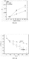
FIG. 2A shows the change in luminous flux (LF) as a function of time for LED components containing uncoated and coated Mn-activated potassium fluorosilicate particles during a high temperature storage (HTS) test. -
FIG. 2B shows the change in u' color point as a function of time for LED components containing uncoated and coated Mn-activated potassium fluorosilicate particles during a HTS test. -
FIG. 2C shows the change in v' color point as a function of time for LED components containing uncoated and coated Mn-activated potassium fluorosilicate particles during a HTS test. -
FIG. 3A shows the change in luminous flux ratio (LF ratio) as a function of time for LED components containing uncoated and coated Mn-activated potassium fluorosilicate particles during a high temperature operating life (HTOL) test. -
FIG. 3B shows color shift as a function of time for LED components containing uncoated and coated Mn-activated potassium fluorosilicate particles during a HTOL test. -
FIG. 4 shows the results of mass loss experiments on cured, free-standing silicone disks stored at 195°C and containing: no phosphor; uncoated Mn-activated potassium fluorosilicate particles; and silica-coated Mn-activated potassium fluorosilicate particles. -
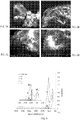
FIGs. 5A to 5D show scanning electron microscope (SEM) images at 5000x magnification of silica-coated Mn-activated potassium fluorosilicate particles with increasing shell (coating) thickness. -
FIG. 6 shows Fourier-transform infrared spectroscopy (FTIR) absorption spectra for the coated particles ofFIGs. 5A-5D , where the inset shows detail of SiOx and SiFx absorption signals corresponding to the silica groups of the coating and the SiF6 2- of the potassium fluorosilicate particles. -
FIG. 7A shows an exemplary light emitting device comprising an LED chip in optical communication with a stabilized fluoride phosphor. -
FIGs. 7B-7D show exemplary packaging configurations for a light emitting device including an LED chip and a stabilized fluoride phosphor. -
FIGs. 8A-8E show exemplary light fixtures that may utilize the light emitting devices and stabilized fluoride phosphor described herein. - An "activator" of a phosphor comprising a host crystal may be understood to be a doping agent, or "dopant," in the host crystal. For example, a transition metal element such as manganese may function as a dopant or activator for a host crystal comprising a fluoride compound. The activator may be utilized to obtain certain luminescence properties from the phosphor.
- What is referred to as "color shift" may be expressed using du' and dv', which describe the chromaticity shift in the CIE 1976 chromaticity diagram (u', v'), where for example du'(x) = u'(t=x) - u'(t=0), and similarly for dv'.
- A first device that is described as being "in optical communication with" a second device may be understood to be positioned such that light from the first device reaches the second device, or vice versa.
- "Dominant wavelength" refers to the wavelength of light that has the same apparent color as the light emitted from an LED, as perceived by the human eye. The dominant wavelength differs from peak wavelength in that the dominant wavelength takes into account the sensitivity of the human eye to different wavelengths of light.
- It is understood that when an element such as a layer, region, or substrate is referred to as being "on" another element, it can be directly on the other element or intervening elements may also be present. Furthermore, relative terms such as "inner," "outer," "upper," "above," "over," "overlying," "beneath," "below," "top," "bottom," and similar terms, may be used herein to describe a relationship between elements. It is understood that these terms are intended to encompass orientations of the device that differ from those depicted in the figures.
- Although the terms first, second, etc. may be used herein to describe various elements, components, regions, layers and/or sections, these elements, components, regions, layers and/or sections should not be limited by these terms. These terms are only used to distinguish one element, component, region, layer or section from another region, layer or section. Thus, a first element, component, region, layer or section discussed below could be termed a second element, component, region, layer or section without departing from the teachings of the present disclosure.
- The figures are intended as schematic illustrations. As such, the actual dimensions and shapes of the devices and components (e.g., layer thicknesses) can be different, and departures from the illustrations as a result of, for example, manufacturing techniques and/or tolerances may be expected. Embodiments should not be construed as limited to the particular shapes of the regions illustrated herein but are to include deviations in shapes that result from, for example, manufacturing. A region illustrated or described as square or rectangular may have rounded or curved features due to normal manufacturing tolerances. Thus, the regions illustrated in the figures are schematic in nature and their shapes are not intended to illustrate the precise shape of a region of a device and are not intended to limit the scope of the invention.
- The terminology used herein is for the purpose of describing particular embodiments only and is not intended to be limiting of the invention. As used herein, the singular forms "a", "an" and "the" are intended to include the plural forms as well, unless the context clearly indicates otherwise. The terms "elements" and "a plurality of elements" may be understood to refer to "more than one element," where "element" may be replaced with any noun. It may be further understood that the terms "comprises" "comprising," "includes" and/or "including" specify the presence of stated features, integers, steps, operations, elements, and/or components, but do not preclude the presence or addition of one or more other features, integers, steps, operations, elements, components, and/or groups thereof.
- Unless otherwise defined, all terms (including technical and scientific terms) used herein have the same meaning as commonly understood by one of ordinary skill in the art to which this invention belongs. It will be further understood that terms used herein should be interpreted as having a meaning that is consistent with their meaning in the context of this specification and the relevant art and will not be interpreted in an idealized or overly formal sense unless expressly so defined herein.
- This disclosure describes a stabilized fluoride phosphor for light emitting diode (LED) applications and a scaleable and cost-effective sol-gel process to prepare the stabilized fluoride phosphor. A manganese-activated fluoride phosphor in particulate form is coated with an inorganic coating comprising a silicate, which acts as a protective shell for the phosphor. When the coated phosphor particles are incorporated into LEDs, the inorganic coating serves both to (a) protect the phosphor from atmospheric oxygen and moisture and (b) protect the LED component and its constituent materials from the corrosive action of fluorine-containing byproducts. The inorganic coating can enhance the stability of LED components containing fluoride-based phosphors, overcoming one of the primary barriers to widespread commercial adoption of such phosphors in solid-state lighting.
- Referring to the schematic of
FIG. 1A , the stabilizedfluoride phosphor 100 includes aparticle 102 comprising manganese-activated potassium fluorosilicate and aninorganic coating 104 on theparticle 102. Theinorganic coating 104 comprises a silicate and functions as an impermeable or nearly impermeable barrier to water and/or oxygen. A silicate may be understood to be a compound comprising silicon and oxygen; one example, the silicate comprises SiOx, where 0.5 ≤ x ≤ 2.5. The SiOx may be referred to as silica, a silica network or, more specifically, amorphous silica. Theinorganic coating 104 may further include Si-OH groups as a consequence of the solution-phase coating process, which is described in detail below. The manganese-activated potassium fluorosilicate may be manganese-activated K2SiF6, which may be referred to as K2SiF6:Mn or KSF:Mn. - For practical applications, the stabilized
fluoride phosphor 100 includes a number of theparticles 102. During the coating process, theparticles 102 are suspended and deagglomerated in a reaction mixture such that theinorganic coating 104 forms on eachparticle 102. Preferably, theinorganic coating 104 conformally coats each of theparticles 102. As would be recognized by the skilled artisan, a conformal coating is one that conforms to the particle surface and may fully encapsulate theparticle 102. Thecoating 104 may range in thickness from about 5 nm to about 2 microns, depending on the duration of the sol-gel reaction and the relative amounts of the reagents employed.Thicker coatings 104 may improve the stability of theparticle 102, as further discussed below. Accordingly, a preferred thickness range may be from about 0.1 µm to about 2 µm. - The stabilized
fluoride phosphor 100 further comprises afluoride layer 106 between theparticle 102 and theinorganic coating 104, as illustrated inFIG. 1B . Thefluoride layer 106 may help to improve the thermal and chemical stability of the phosphor. Thefluoride layer 106 may comprise potassium fluorosilicate (e.g., K2SiF6) without an activator, or another fluoride compound. The fluoride layer may have a thickness in a range from about 5 nm to about 5 microns. - The manganese-activated potassium fluorosilicate particles are commercially available. Typically, the particles have a nominal size (width or diameter) in a range from about 5 microns to about 30 microns.
- As a demonstration of the improvement in stability achieved for the K2SiF6:Mn ("KSF:Mn") phosphor when coated with a silicate as described, high temperature storage (HTS) tests are carried out on LED components including coated and uncoated phosphors. HTS testing can be used to evaluate the reliability of the LED components during long-term storage at elevated temperatures. A series of warm-white, 90 CRI (color rendering index) LED components are fabricated, where half the components include an uncoated KSF:Mn phosphor and the other half include a coated KSF:Mn phosphor. In this example, the coating comprises silica, as described above. The components are subjected to an HTS test at 195°C for approximately 400 hours.
- After 400 hours, the LED components prepared with the uncoated KSF:Mn phosphor have degraded significantly, dropping to about 70% of initial luminous intensity and showing about 15 steps of u' and v' color shift, as shown in
FIGs. 2A-2C , where each step is 0.001 in either u' or v' space. In contrast, the LED components prepared with the silica-coated KSF:Mn phosphor shifted by only about 3 steps in u', 7 steps in v', and retained greater than 90% of initial luminous intensity over the same test period. This enhancement in stability is attributed to the ability of the silica shell to protect the KSF:Mn particles from degradation and isolate the LED component from the corrosive action of fluoride species. - High temperature operating life (HTOL) tests are carried out to evaluate the reliability of LED components including silica-coated and uncoated phosphors. The impact of the phosphor coating in a Cree MHB-B component at a color temperature of 3000K and 90 CRI operating at 700 mA and 9 V (nominally 6.3 W), with a heat sink and ambient temperature of 85°C is investigated. Referring to
FIGs. 3A and3B , the results show an improvement in both luminous flux (LF ratio) stability and color shift stability (attributed to silicone stability). - In another demonstration, cured, free-standing silicone disks are prepared containing no phosphor, uncoated KSF:Mn phosphor, and silica-coated KSF:Mn phosphor. Silicone is commonly employed as an encapsulant for LEDs with phosphor particles dispersed in the silicone to effect down-conversion of light emitted from the LED. The silicone disks are stored at 195°C and their weight is monitored over time. Referring to
FIG. 4 , the data show that the disk prepared with uncoated KSF:Mn loses more than 50% of its initial mass after 550 hours. Disks prepared with thin or partial coatings of silica on the KSF:Mn particles, where the coatings are estimated to be less than 100 nm in thickness, show a small improvement in one example and almost no improvement in another. In contrast, the disks prepared with thicker coatings on the KSF:Mn particles lose only 10% and 20% of their initial mass. The thicker coatings are estimated to be at least 100 nm in thickness and as thick as 2 microns. For reference, a silicone disk containing no phosphor loses about 10% of its mass over the same period. In addition to being measured, the mass loss may be visually observed as shrinkage of the disks. The results suggest that uncoated KSF:Mn has a severe chemical interaction with the silicone resulting in significant degradation and mass-loss. This degradation is associated with a positive dv' color shift in components. Application of a silica coating effectively reduces this interaction and slows the rate of mass loss significantly. -
FIGs. 5A to 5D show scanning electron microscope (SEM) images at 5000x magnification of silica-coated Mn-activated potassium fluorosilicate particles with increasing shell (coating) thickness.FIG. 6 shows FTIR absorption spectra in attenuated total reflection (ATR) mode for the coated phosphor particles shown inFIGs. 5A to 5D pressed onto the ATR crystal. The stabilized fluoride phosphor has a first feature in the infrared absorption spectrum at about 850 cm-1 associated with the fluorosilicate (SiF6 2-) content of the sample and a second feature in the infrared absorption spectrum between about 1020 cm-1 and 1070 cm-1 corresponding to the SiOx content of the sample. A ratio of the absorption intensity of the SiOx feature to the SiF6 2- feature is between about 0.05 and 2.5, with larger ratios indicating thicker silica coatings. There is a link between coating thickness and phosphor stability as discussed above and suggested by the data ofFIG. 4 ; however, thinner coatings may be preferred from a processing and materials standpoint. Accordingly, it may be preferred that the ratio of the maximum absorption intensity SiO2 feature to the SiF6 2- is at least about 0.5, at least about 1, or at least about 1.5. For some applications, however, the ratio may be no higher than 1.5, no higher than 2, or no higher than 2.5. - Other experiments indicate that photoluminescence quantum yield (PLQY) of the KSF:Mn phosphor is largely unchanged upon deposition of the silica coating; the PLQY after coating is ≥95% of the value prior to coating.
- The composition of the inorganic coating may be modified by incorporating organic residues (e.g., carbon) into the silica network. This may be accomplished by using organosilane precursors during the coating process, as described below. Also or alternatively, nitrogen or sulfur may be included in the inorganic coating by selecting an appropriate silane precursor.
- For some applications, the inorganic coating may comprise a multicomponent silicate including aluminum, boron, and/or titanium. Also or alternatively, the inorganic coating may comprise an oxide of aluminum, boron, and/or titanium, such as an aluminate, a borate, or a titanate.
- It is contemplated that the KSF:Mn phosphor may be replaced with any water-soluble salt, which may or may not function as a phosphor. The above-described coating method provides a low-water and low-polarity environment that may be suitable for the growth of an inorganic coating comprising a silicate on a variety of ionic solids, including various chlorides, bromides, iodides, and fluorides. For example, the method may be used to form an inorganic (e.g., silica) coating on NaCl, Na2SiF6, KF, K2SiF6, K2TiF6, Rb2SiF6, CS2GeF6, Cs2SiF6, Cs2MnF6, Cs2SnF6, MgCl2, and other salts. In general, suitable salts may have a chemical formula AxByCz, where x is from about 1 to about 2, y is from about 1 to about 2, and z is about 6, and where A is selected from Na, K, Cs, Ca, Sr, and Ba, B is selected from Si, Ge, Sn, Ti, and Al, and C is selected from F and CI. Such compounds are easily dissolved in water and thus may be difficult to coat using typical solution methods. Thus, in an alternative example that is useful for understanding the invention but not presently claimed, the method may yield a stabilized salt including particles comprising a water-soluble salt and an inorganic coating on each of the particles, where the inorganic coating comprises silicate, such as SiOx (0.5 ≤ x ≤ 2.5). The inorganic coating of the water-soluble salt may have any of the characteristics described above or elsewhere in this disclosure for the stabilized fluoride phosphor.
- The method developed to form the stabilized fluoride phosphor (or the stabilized salt) may be described as a sol-gel method.
- The method comprises, according to the presently claimed invention, forming a reaction mixture that includes the following reagents: particles comprising a manganese-activated potassium fluorosilicate; a reactive silicate precursor; a catalyst; a solvent; and water in an amount no greater than about 10% by volume. The reaction mixture is agitated to suspend the particles therein. As the reactive silicate precursor undergoes hydrolysis and condensation in the reaction mixture, an inorganic coating comprising a silicate is formed on the particles, thereby forming a stabilized fluoride phosphor comprising silicate-coated, manganese-activated fluorosilicate particles.
Table 1. Exemplary volumes of reagents (per gram of phosphor) Volume Solvent (ml/g) Volume Water (ml/g) Volume silicate precursor (e.g., TEOS) per addition (ml/g) Volume Catalyst (ml/g) Low 5 0.2 0.12 0.20 High 60 2 3 3.5 Preferred 20 to 40 0.3 to 1 0.3 to 1.5 0.5 to 2 - According to another example that is useful for understanding the invention but not presently claimed, the method comprises forming a reaction mixture that includes the following reagents: particles comprising a water-soluble salt; a reactive silicate precursor; a catalyst; a solvent; and water in an amount no greater than about 10% by volume. The reaction mixture is agitated to suspend the particles therein. As the reactive silicate precursor undergoes hydrolysis and condensation in the reaction mixture, an inorganic coating comprising a silicate is formed on the particles, thereby forming a stabilized salt comprising silicate-coated, water-soluble salt particles. In one embodiment, the silicate comprises SiOx, where 0.5 ≤ x ≤ 2.5.
- The synthesis and processing description below may in some cases refer specifically to the stabilized fluoride phosphor of the first embodiment. However, it is understood that the description below also applies more generally to the stabilized salts of the second embodiment. In other words, each synthesis or processing step described below can be applied to either the manganese-activated potassium fluorosilicate particles in particular or to the water-soluble salt particles in general. As mentioned above, the stabilized salt formed in the process may or may not behave as a phosphor.
- The method may be carried out by adding some or all of the reagents, in particular the reactive silicate precursor, to the reaction mixture gradually, e.g., over minutes, hours, or days. For example, one or more of the reagents may be added in portions over several days, or one or more of the reagents may be continuously infused into the reaction mixture using a pump.
- After formation of the stabilized fluoride phosphor or the stabilized salt, the silicate-coated particles may be washed in tetrahydrofuran or isopropanol for purification, or separation from the catalyst, solvent, and any unreacted silicate precursor. Preferably, the reaction mixture is largely devoid of free silicate in particulate form; most or all of the silicate formed in the reaction may be conformally adhered to the surface of each particle. It is noted that even after removal from the reaction mixture, condensation of the silicate may continue to occur and thus the inorganic coating may continue to form outside the reaction mixture; that is, the inorganic coating may increase in thickness and/or density after removal of the particles from the reaction mixture. The particles may undergo drying at a temperature in a range from about 40°C to about 200°C to remove any volatile species left over from the synthesis.
- Gentle agitation may be employed to disperse and suspend the particles in the reaction mixture. Unlike conventional oxide, nitride, and sulfide phosphors, the fluoride phosphor may be quite brittle due to its ionic chemical composition. To ensure a uniform coating, the reaction mixture may be agitated to mix and suspend the particles therein; however, if this agitation is not done carefully, damage to the particles may result. Even moderate stirring with a magnetic stirbar may be sufficient to severely damage the particles over the typically long reaction times. To address this issue, a variety of gentle stirring methods that can suspend the particles in the reaction mixture without damaging them may be employed. A first method uses an orbital shaker to agitate the reaction vessel externally. In this case, the phosphor particles are in contact only with the vessel walls and the reaction mixture. A second method uses an overhead motor to drive an impeller. With careful selection of the impeller shape, the particles can be suspended with minimal shear, thereby reducing damage. In addition to orbital shaking and overhead stirring with an impeller, tumbling, and/or magnetic stirring may be employed.
- The catalyst may be a basic or acidic catalyst. It is preferred that a nonaqueous catalyst is employed for the reaction instead of the aqueous acids or bases typically used in sol-gel methods. For example, the basic catalyst may comprise an organic amine, such as diisopropylethylamine (DIPEA) or triethylamine (TEA). As mentioned above, KSF:Mn is unstable towards water, yet water is typically a necessary reagent in silicate-forming sol-gel processes; thus, its concentration may be a critical parameter. By using a nonaqueous catalyst, the concentrations of water and the catalyst can be independently controlled in the reaction mixture. For example, a coating reaction can be performed with an arbitrarily high catalyst loading and a stoichiometric quantity (or even less) of water. In contrast, concentrated ammonia and hydrochloric acid, which are aqueous basic and acidic catalysts, respectively, are about 65% water by weight. It is noted that the catalyst and the reactive silicate precursor may in some cases be part of the same molecule. An example is aminopropyltriethoxysilane (APTES), which includes triethoxysilane, an exemplary silicate precursor, and an amine, an exemplary catalyst.
- The water employed as a reagent may be independently added to the reaction mixture as a liquid. Alternatively, the water may be incorporated into the reaction mixture with the solvent, where it may be present as an impurity. In another example, the water may be added to the reaction mixture via a moisture-containing gas stream or by diffusion from the atmosphere, which may have a controlled humidity level.
- The solvent is preferably miscible with all the reagents used in the reaction and has low to moderate polarity. The solvent may comprise an organic solvent such as tetrahydrofuran, toluene, or isopropanol. The solvent may be rigorously dried prior to incorporation in the reaction mixture to ensure that unwanted water is not added. If the concentration of water in the reaction mixture is too high (e.g., greater than about 10 vol.%), the silicate may nucleate rapidly away from the surface of the particles, which is undesirable. Saturated toluene at 80% relative humidity and room temperature (20-25°C) may provide a practical limit for water concentration.
- The reactive silicate precursor may be selected from tetraethylorthosilicate (TEOS), tetramethylorthosilicate (TMOS), and tetrapropylorthosilicate (TPOS), or combinations of these. The reactive silicate precursor may comprise a reactive silica precursor. The inorganic coating may be modified by incorporation of organic residues into the silica network. Thus, the method may include adding an organosilane to the reaction mixture. For example, to add carbon to the inorganic coating, the reactive silicate precursor may comprise methyl-, ethyl-, or propyltriethoxysilane, thereby incorporating methyl, ethyl, or propyl groups, respectively. To incorporate nitrogen or sulfur to the coating, the reactive silicate precursor may comprise 3-aminopropyltriethoxysilane or 3-mercaptopropyltriethoxysilane.
- An organosilane may also or alternatively be employed prior to the coating reaction to bond with the particles and act as an adhesion promoter for formation of the coating. Thus, the method may include, prior to forming the reaction mixture, exposing the phosphor particles to an organosilane or other adhesion promoter. Typically, the particles are mixed with the organosilane and stirred for a period of time before adding other reagents to the reaction mixture. Suitable organosilanes have a head group that binds or coordinates to the surface of the KSF:Mn particles and a tail group that can react with additional silicate-forming precursors, such as TEOS. Examples of suitable adhesion promoters are 3-aminopropyltriethoxysilane (3-APTES) and 3-mercaptopropyltriethoxysilane (3-MPTES). These molecules have amine and thiol head groups, respectively, and triethoxysilane tail groups.
- The inorganic coating may include multicomponent silicates, borates, aluminates, and/or titanates. In other words, the coating may comprise a silicate including the elements silicon and oxygen, and may further comprise a multicomponent silicate, borate, aluminate, or titanate, as indicated above. Or, the silicate of the inorganic coating, which includes the elements silicon and oxygen, may further include additional elements, such as boron, aluminum and/or titanium, and thus the silicate may be referred to as a multicomponent silicate. Accordingly, the method may further comprise adding a reactive metal oxide precursor comprising boron, aluminum and/or titanium to the reaction mixture. For example, the reactive metal oxide precursor may comprise an alkoxide, such as boron alkoxide, aluminum alkoxide and/or titanium alkoxide.
- After forming the stabilized fluoride phosphor, the silicate-coated particles may be heated or annealed at an elevated temperature (e.g., from about 200°C to 700°C) for a suitable time duration to densify the coating. For example, the annealing may be carried out for a time duration from about 5 mins to 72 hours, preferably in a controlled environment. The annealing may be carried out in an inert gas, in oxygen/air, or in a reducing atmosphere. Annealing the stabilized phosphor in this way may reduce porosity in the coating, transform Si-OH bonds to silica bonds, and improve the protective ability of the coating.
- A secondary inorganic coating, such as an oxide coating or shell, may be deposited on the (primary) inorganic coating. The secondary inorganic coating may have a substantially identical composition to the primary inorganic coating and merely increase the silicate thickness, or the secondary inorganic coating may have a different composition and/or different properties compared to the primary inorganic coating. For example, the primary inorganic coating may have higher porosity and lower density while the secondary inorganic coating may have lower porosity and higher density. Furthermore, the primary and secondary inorganic coatings may be prepared by different processes. For example, a primary inorganic coating of silica may be prepared using a base catalyst and an excess of water whereas a secondary inorganic coating of silica may be prepared using an acid catalyst and a stoichiometric amount of water; the base catalyst may be a nonaqueous catalyst, while the acid catalyst used to form the secondary inorganic coating may be an aqueous catalyst.
- In a nitrogen glovebox, 500 mg of KSF:Mn is added to an oven-dried glass vial along with 15 ml of dry tetrahydrofuran (THF) and 0.440 ml of diisopropylethylamine. The vial is sealed with a septum-cap and brought out of the glovebox. 0.250 ml tetraethylorthosilicate (TEOS) is then added through the septum followed by 0.240 ml of water. The vial is then agitated using an orbital shaker to suspend the KSF particles in the reaction mixture. Additional portions of 0.250 ml of TEOS are added after 24 and 48 hours. After 72 hours, the silica-coated particles are collected by centrifugation and washed twice with 15 ml THF. The stabilized fluoride phosphor is then air-dried for 1 hour, and then dried in an oven at 70°C for 1 hour.
- In a large polypropylene cup, 5.0 g KSF:Mn is combined with 150 ml of water-saturated toluene and 6.0 ml 3-APTES. The mixture is stirred for 20 hours to allow the adhesion promoter to adhere to the particle surface. 1.0 ml TEOS is then added, followed by two additional portions of TEOS at 24 and 48 hours following the first addition. 24 hours after the final addition of TEOS, the silica-coated product is collected by centrifugation and washed two times with toluene. The stabilized fluoride phosphor is then dried at 80 °C for 2 hours.
- The above-described stabilized fluoride phosphor may be employed in various light emitting devices, such as illumination-class, phosphor-converted warm-white LEDs (both mid- and high-power), especially those with a color-rendering index (CRI) greater than 90. Such LEDs are well-suited for application in high-quality indoor lighting products, which combine high color quality and high efficacy. In addition, the stabilized fluoride phosphor may be used instead of or in combination with conventional phosphors in phosphor-converted red LEDs (e.g., pc-red). Examples of such lighting products are discussed below. It is also worth noting that, due to its narrow-band red emission, the silica-coated KSF:Mn phosphor may be used in display backlighting for TVs, monitors, tablets, and smart phones. Finally, the stabilized fluoride phosphor may be useful for certain horticultural lighting applications, where a narrow red-emission band could be targeted to specific plant absorptions (e.g., chlorophyll A, chlorophyll B, phytochrome).
- As mentioned above, the stabilized fluoride phosphor may be employed in a light emitting device, such as that shown schematically in
FIG. 7A . Thelight emitting device 720 may include a blue light emitting diode (LED)chip 730 having a dominant wavelength of 420 nm to 490 nm in optical communication with a wavelength conversion material comprising the stabilized fluoride phosphor 700 (which may have any of the characteristics described above or elsewhere in this disclosure) for down conversion of light emitted from theblue LED chip 730. The light emitting device may exhibit narrow-band red light emission with a peak emission wavelength in a range from 610 nm to 660 nm and a full-width-at-half-maximum (FWHM) of less than 45 nm. - The
blue LED chip 730 may be disposed on a submount (substrate) 740 and a lens or encapsulant 750 may overlie theLED chip 730, although other submount or package configurations are possible as described below. - The stabilized
fluoride phosphor 700 may be employed in any of a number of configurations. For example, a coating on the LED chip may include the stabilizedfluoride phosphor 700, as illustrated inFIG. 7A . Alternatively, a lens overlying the LED chip or an encapsulant on the LED chip may include the stabilized fluoride phosphor. For example, the stabilizedfluoride phosphor 700 may be coated on an inner or outer surface of the lens, or the composite 700 may be dispersed throughout the volume of the encapsulant. In another example, a substrate disposed remote from the LED chip may include the stabilized fluoride phosphor. More than one type of LED chip (blue and/or other colors) as well as additional phosphors and/or luminescent semiconducting nanoparticles (quantum dots) may be employed in thelight emitting device 720. - For example, the wavelength conversion material may further comprise a plurality of quantum dots, such as the stabilized quantum dots described in
U.S. Patent 9,780,266 - The light emitting device may have any of a number of different packaging configurations. As is well known in the art, in order to use an LED chip in a circuit or other like arrangement, it is known to enclose the LED chip in a package to provide environmental and/or mechanical protection, color selection, light focusing and the like. An LED package may also include electrical leads, contacts or traces for electrically connecting the LED package to an external circuit.
- A
typical LED package 10 is illustrated inFIG. 7B . In this example, asingle LED chip 12 is mounted on a reflective cup 13 by means of a solder bond or conductive epoxy. One ormore wire bonds 11 connect the contacts of theLED chip 12 to leads 15A and/or 15B, which may be attached to or integral with the reflective cup 13. The reflective cup may be filled with anencapsulant material 16 which may contain a wavelength conversion material such as the stabilized fluoride phosphor. The entire assembly may be encapsulated in aprotective resin 14, which may be molded in the shape of a lens to collimate the light emitted from theLED chip 12. - Another
conventional LED package 20 is illustrated inFIG. 7C and includes one ormore LED chips 22 mounted onto a carrier, such as a printed circuit board (PCB) carrier, as well as leads and a substrate or submount. In this embodiment, areflector 24 mounted on asubmount 23 surrounds the LED chip(s) 22 and reflects light emitted by the LED chip(s) 22 away from thepackage 20. Thereflector 24 also provides mechanical protection to the LED chips 22. One or morewirebond connections 27 may be made between contacts on the LED chips 22 andelectrical traces 25A, 25B on thesubmount 23. The mountedLED chips 22 are then covered with anencapsulant 26, such as a silicone, which may provide environmental and mechanical protection to the chips while also acting as a lens. As described above, the encapsulant may contain wavelength conversion material(s), such as the stabilized fluoride phosphor described herein. Other exemplary LEDs comprise LED packages formed of a plastic material that is molded about a lead frame, and the LED chip(s) is mounted in a cavity of the package, and an optically transmissive encapsulant, such as silicone, is dispensed into the cavity over the LED chip(s). Again, wavelength conversion material(s) such as the stabilized fluoride phosphor can be dispersed in the encapsulant. - Another exemplary LED package 30 is shown in
FIG. 7D and comprises an LED chip 34 on a submount 32 with a moldedlens 70, such as a silicone lens, formed over it. Thelens 70 can include wavelength conversion material(s), such as the stabilized fluoride phosphor described herein, dispersed therein and/or on the LED chip. The LED chip 32 can also be coated by a conversion material that can convert all or most of the light from the LED. The lens can be molded in different shapes, such as hemispherical, planar, chopped or other shapes. An example of such LEDs is described inU.S. Patent Nos. 9,070,850 9,048,396 FIG. 7D are defined inU.S. Patent No. 9,070,850 U.S. Patent No. 8,624,271 . - LED chips generally comprise one or more active layers of semiconductor material sandwiched between oppositely doped layers. When a bias is applied across the doped layers, holes and electrons are injected into the active layer where they recombine to generate light. Light is emitted from the active layer and from various surfaces of the LED. Light is emitted by the LED chip at a primary wavelength. The primary radiation may be absorbed by the wavelength conversion material (e.g., the stabilized fluoride phosphor), which responsively emits light at secondary wavelength(s). The primary and/or secondary wavelengths of light can mix to produce a desired color of light. As would be understood by one of skill in the art, depending on the primary wavelength(s) and the amount of loading of the wavelength conversion material(s), as well as their light absorption/emission characteristics, various color temperatures of white light can be produced by the LEDs.
- The LED chips shown schematically in
FIGs. 7A-7D may be group III nitride-based LED chips whose active region is formed from nitrogen and group III elements such as aluminum, gallium and/or indium in the form of nitride layers epitaxially grown and doped, as would be understood by one of ordinary skill in the art, to produce light in the green to UV spectral ranges, for example blue light. As illustrated in the preceding examples, the stabilized fluoride phosphor may be incorporated into silicone or another optically transparent encapsulant material and coated onto the LED chip. In other embodiments, the stabilized fluoride phosphor can be placed in and/or on an encapsulant and/or optic of the LED chip, such as silicone, epoxy or glass. Also, phosphors, such as red nitride phosphors and/or green or yellow LuAG or YAG phosphors, can be mixed together with the stabilized fluoride phosphor in the matrix and/or positioned separately (e.g., in a remote phosphor configuration) on the optic and/or in discrete layers on the LED chip. The result may be a light emitting device that emits warm white light (e.g., 2700K to 4000K) and/or comprises a high CRI (e.g., greater than 90) and/or has an increased gamut. - The LED components, packages and light emitting devices described above may be fabricated using methods known in the art, as described for example in
U.S. Patent Application Publication No. 2012/0280261 , entitled "Light Emitting Diode (LED) for Achieving an Asymmetric Light Output". In addition, the blue LED chips may be coated with the aforementioned stabilized fluoride phosphor using any suitable method, such as that describedU.S. Patent Application Publication Nos. 2008/0179611 and2008/0173884 , both of which are entitled "Wafer Level Phosphor Coating Method and Devices Fabricated Utilizing Method". As set forth in these patent publications, LED chips can be coated and/or sprayed by phosphors such as the stabilized fluoride phosphor described herein (e.g., in the form of microparticles), and/or other wavelength conversion materials. The LED chips may also be coated using electrophoretic deposition (EPD), such as with the EPD method described inU.S. Patent No. 8,563,339 to Tarsa et al. , entitled "Closed Loop Electrophoretic Deposition of Semiconductor Devices". - The light emitting devices comprising the stabilized fluoride phosphor described herein may have particular utility with respect to various form factor light fixtures. For example, each of the embodiments disclosed herein may be alternatively implemented in various types of solid state light fixtures including, for example, downlights, troffers, street lights, canopy lights, parking garage lights, lights that use waveguide technology and other lighting fixtures.
FIG. 8A illustrates an omnidirectional light bulb, such as an A19 bulb. Other similar consumer lights, such as PAR, BR and candelabra bulbs, can also implement the light emitting devices described herein. Exemplary lights are described inU.S. Patent Nos. 8,591,062 and8,596,819 andU.S. Patent Publication No. 2015/0362168 .FIG. 8B shows another downlight that can incorporate light emitting devices described herein. An example of such a downlight is disclosed inU.S. Patent No. 8,777,449 .FIG. 8C illustrates a troffer light fixture that can incorporate the light emitting devices described herein. An exemplary troffer light fixture is disclosed in U.S. Published Patent Publication No.US2012/0327650 . In another example,FIG. 8D illustrates a solid state street light that may include the light emitting devices described herein. Other street lights and outdoor lighting fixtures that can be implemented using the light-emitting devices described herein include the lights disclosed inU.S. Patent No. 8,622,584 ;U.S. Patent No. 8,425,071 ;U.S. Patent No. 9,028,087 U.S. Patent Publication No. 2015/0253488 . Finally,FIG. 8E illustrates a canopy light which is described inU.S. Patent No. 9,182,096 U.S. Patent Publication No. 2014/0347885 , in the troffer style fixtures disclosed inU.S. Patent Publication No. 2012/0051041 and/or in the waveguide-based garage lights disclosed inU.S. Patent Publication No. 2014/0355302 . Other and similar light fixtures can be implemented using the above-described circuitry. - As known to those skilled in the art, lamps have been developed utilizing solid state light sources, such as LEDs, in combination with a conversion material that is separated from or remote to the LEDs. Such arrangements are disclosed in
U.S. Patent No. 6,350,041 , entitled "High Output Radial Dispersing Lamp Using a Solid State Light Source". Suitable lamps can comprise a solid state light source that transmits light through a separator to a disperser including one or more phosphors and/or the stabilized fluoride phosphor. The disperser can disperse the light in a desired pattern and/or changes its color by converting at least some of the light to a different wavelength through the phosphor(s), stabilized fluoride phosphor, and/or other wavelength conversion material. In some embodiments, the separator spaces the light source a sufficient distance from the disperser such that heat from the light source will not transfer to the disperser when the light source is carrying elevated currents necessary for room illumination. Additional remote phosphor techniques are described inU.S. Patent No. 7,614,759 , entitled "Lighting Device". - Although the present invention has been described in considerable detail with reference to certain embodiments thereof, other embodiments are possible without departing from the present invention. The scope of the appended claims should not be limited, therefore, to the description of the preferred embodiments contained herein. All embodiments that come within the meaning of the claims are intended to be embraced therein.
Claims (15)
- A stabilized fluoride phosphor (100, 700) for light emitting diode, LED, applications, the stabilized fluoride phosphor (100, 700) comprising:particles (102) comprising manganese-activated potassium fluorosilicate; andan inorganic coating (104) on each of the particles (102), the inorganic coating (104) comprising a silicate, and a fluoride coating under the inorganic coating (104).
- The stabilized fluoride phosphor (100, 700) of claim 1, wherein the silicate comprises: a multicomponent silicate including aluminum, boron, and/or titanium; and/or SiOx, where 0.5 ≤ x ≤ 2.5.
- The stabilized fluoride phosphor (100, 700) of claim 1 or 2, wherein:the inorganic coating (104) comprises a thickness in a range from about 5 nm to about 2 microns, preferably wherein the thickness is in the range from about 0.1 micron to about 2 microns; and/orthe inorganic coating (104) further comprises: Si-OH groups; and/or an oxide of aluminum, boron, and/or titanium.
- The stabilized fluoride phosphor (100, 700) of any one of claims 1-3, comprising an infrared absorption spectrum wherein a ratio of an absorption intensity of a SiOx signal to an absorption intensity of a SiF6 2-signal is in a range from about 0.05 to about 2.5.
- A light emitting device (720) comprising:
a blue light emitting diode, LED, chip (730) having a dominant wavelength of 420 nm to 490 nm in optical communication with a wavelength conversion material comprising the stabilized fluoride phosphor (100, 700) of any one of claims 1-4 for down conversion of light emitted from the blue LED chip (730). - The light emitting device (720) of claim 5 exhibiting narrow-band red light emission with a peak emission wavelength in a range from 610 nm to 660 nm and comprising a full-width-at-half-maximum, FWHM, of less than 45 nm.
- The light emitting device (720) of claim 5 or 6, wherein the wavelength conversion material further comprises a plurality of quantum dots.
- The light emitting device of any one of claims 5-7, wherein:the wavelength conversion material further comprises a yellow phosphor exhibiting yellow light emission with a peak emission wavelength in a range from 575 nm to 600 nm, preferably wherein the yellow light emission has a full-width-at-half-maximum, FWHM, of less than 60 nm, the yellow light emission being narrow band yellow light emission; and/orthe wavelength conversion material further comprises a green phosphor exhibiting green light emission with a peak emission wavelength in a range from 498 nm to 550 nm, preferably wherein the green light emission has a full-width-at-half-maximum, FWHM, of less than 60 nm, the green light emission being narrow band green light emission.
- The light emitting device of any one of claims 5-8 used in at least one of the following: indoor lighting products; display backlighting for televisions, monitors, tablets or smart phones; and horticultural lighting products.
- A method of making a stabilized fluoride phosphor (100, 700), the method comprising:forming a reaction mixture comprising:particles (102) comprising a manganese-activated potassium fluorosilicate,a reactive silicate precursor,a catalyst,a solvent, andwater in an amount no greater than about 10 vol.%, and agitating the reaction mixture to suspend the particles (102) therein,wherein, as the reactive silicate precursor undergoes hydrolysis and condensation in the reaction mixture, an inorganic coating (104) comprising a silicate is formed on each of the particles (102), thereby forming a stabilized fluoride phosphor (100, 700).
- The method of claim 10, wherein the agitating employs a technique selected from the group consisting of: magnetic stirring, overhead stirring with an impeller, orbital shaking, and tumbling.
- The method of claim 10 or 11, wherein:the reactive silicate precursor comprises an organosilane precursor; and/orthe reactive silicate precursor comprises a silane selected from the group consisting of: tetraethylorthosilicate, TEOS, tetramethylorthosilicate, TMOS, and tetrapropylorthosilicate, TPOS, andwherein the catalyst comprises a nonaqueous catalyst.
- The method of claim 12, wherein the nonaqueous catalyst comprises an organic amine.
- The method of any one of claims 10-13, wherein:the solvent is dried prior to incorporation in the reaction mixture; and/orprior to adding the catalyst, the solvent, and the water to the reaction mixture, an organosilane precursor is added to the reaction mixture to bond with the particles (102) and act as adhesion promoter for formation of the inorganic coating (104).
- The method of any one of claims 10-14, further comprising:adding a reactive metal oxide precursor comprising boron, aluminum or titanium to the reaction mixture;removing the stabilized fluoride phosphor (100, 700) from the reaction mixture,
wherein, outside the reaction mixture, hydrolysis and condensation continues, the inorganic coating (104) thereby continuing to form; and/orheating the stabilized fluoride phosphor (100, 700) at an elevated temperature in a range from about 200°C to about 700°C to densify the inorganic coating (104).
Applications Claiming Priority (2)
| Application Number | Priority Date | Filing Date | Title |
|---|---|---|---|
| US15/994,105 US10608148B2 (en) | 2018-05-31 | 2018-05-31 | Stabilized fluoride phosphor for light emitting diode (LED) applications |
| PCT/US2019/033718 WO2019231817A1 (en) | 2018-05-31 | 2019-05-23 | Stabilized fluoride phosphor for light emitting diode (led) applications |
Publications (2)
| Publication Number | Publication Date |
|---|---|
| EP3802728A1 EP3802728A1 (en) | 2021-04-14 |
| EP3802728B1 true EP3802728B1 (en) | 2022-07-13 |
Family
ID=66912928
Family Applications (1)
| Application Number | Title | Priority Date | Filing Date |
|---|---|---|---|
| EP19731393.5A Active EP3802728B1 (en) | 2018-05-31 | 2019-05-23 | Stabilized fluoride phosphor for light emitting diode (led) applications |
Country Status (5)
| Country | Link |
|---|---|
| US (3) | US10608148B2 (en) |
| EP (1) | EP3802728B1 (en) |
| JP (1) | JP2021525820A (en) |
| CN (1) | CN112204116B (en) |
| WO (1) | WO2019231817A1 (en) |
Families Citing this family (5)
| Publication number | Priority date | Publication date | Assignee | Title |
|---|---|---|---|---|
| JP6932679B2 (en) * | 2017-11-30 | 2021-09-08 | デクセリアルズ株式会社 | Coated fluorescent material, its manufacturing method, fluorescent material sheet, and light emitting device |
| WO2019107080A1 (en) | 2017-11-30 | 2019-06-06 | デクセリアルズ株式会社 | Coated phosphor, method for producing same, phosphor sheet, and light-emitting device |
| CN112909148A (en) * | 2021-02-08 | 2021-06-04 | 开发晶照明(厦门)有限公司 | Chip-on-board type photoelectric device |
| CN115074110A (en) * | 2021-03-10 | 2022-09-20 | 隆达电子股份有限公司 | Wavelength conversion substance, light-emitting element and display device |
| US12550496B2 (en) | 2022-06-10 | 2026-02-10 | Creeled, Inc. | Coated phosphor particle, light emitting device including a coated phosphor particle, and method of making a coated phosphor particle |
Family Cites Families (57)
| Publication number | Priority date | Publication date | Assignee | Title |
|---|---|---|---|---|
| JPH04178486A (en) * | 1990-11-09 | 1992-06-25 | Sumitomo Chem Co Ltd | Production of water-resistant fluophor |
| US6350041B1 (en) | 1999-12-03 | 2002-02-26 | Cree Lighting Company | High output radial dispersing lamp using a solid state light source |
| KR100366097B1 (en) * | 2000-09-29 | 2002-12-26 | 삼성에스디아이 주식회사 | Phosphors for PDP coated with continuous thin protective layer and preparing process therefor |
| US9070850B2 (en) | 2007-10-31 | 2015-06-30 | Cree, Inc. | Light emitting diode package and method for fabricating same |
| US8563339B2 (en) | 2005-08-25 | 2013-10-22 | Cree, Inc. | System for and method for closed loop electrophoretic deposition of phosphor materials on semiconductor devices |
| JP5443662B2 (en) * | 2005-09-28 | 2014-03-19 | 戸田工業株式会社 | Method for producing moisture-resistant phosphor particle powder and LED element or dispersion-type EL element using moisture-resistant phosphor particle powder obtained by the production method |
| CN101351891B (en) | 2005-12-22 | 2014-11-19 | 科锐公司 | Lighting device |
| JP2009539227A (en) | 2006-05-31 | 2009-11-12 | クリー エル イー ディー ライティング ソリューションズ インコーポレイテッド | Lighting device and lighting method |
| US7820074B2 (en) * | 2006-06-28 | 2010-10-26 | Seoul Semiconductor Co., Ltd. | Phosphor, method for manufacturing same, and light emitting diode |
| US9028087B2 (en) | 2006-09-30 | 2015-05-12 | Cree, Inc. | LED light fixture |
| US7686469B2 (en) | 2006-09-30 | 2010-03-30 | Ruud Lighting, Inc. | LED lighting fixture |
| US9159888B2 (en) | 2007-01-22 | 2015-10-13 | Cree, Inc. | Wafer level phosphor coating method and devices fabricated utilizing method |
| US9024349B2 (en) | 2007-01-22 | 2015-05-05 | Cree, Inc. | Wafer level phosphor coating method and devices fabricated utilizing method |
| KR101414243B1 (en) * | 2007-03-30 | 2014-07-14 | 서울반도체 주식회사 | METHOD FOR COATING SULFIDE PHOSPHOR AND LIGHT EMITTING DEVICE USING COATED SULFIDE PHOSPHOR |
| CA2720313C (en) | 2008-04-04 | 2016-11-08 | Ideal Industries Lighting Llc | Led light fixture |
| US9182096B2 (en) | 2013-03-06 | 2015-11-10 | Cree, Inc. | Light fixture |
| US8777449B2 (en) | 2009-09-25 | 2014-07-15 | Cree, Inc. | Lighting devices comprising solid state light emitters |
| JP2011068791A (en) * | 2009-09-25 | 2011-04-07 | Panasonic Electric Works Co Ltd | Coated phosphor and led light-emitting device |
| JP4991943B2 (en) | 2010-02-26 | 2012-08-08 | キヤノン株式会社 | Optical member, polyimide, and manufacturing method thereof |
| US9614129B2 (en) * | 2010-08-14 | 2017-04-04 | Seoul Semiconductor Co., Ltd. | Light emitting device having surface-modified luminophores |
| US10883702B2 (en) | 2010-08-31 | 2021-01-05 | Ideal Industries Lighting Llc | Troffer-style fixture |
| US8624271B2 (en) | 2010-11-22 | 2014-01-07 | Cree, Inc. | Light emitting devices |
| US9048396B2 (en) | 2012-06-11 | 2015-06-02 | Cree, Inc. | LED package with encapsulant having planar surfaces |
| JP5589896B2 (en) * | 2011-02-28 | 2014-09-17 | 住友金属鉱山株式会社 | Method for producing silicate phosphor particles with coating film |
| US8252613B1 (en) | 2011-03-23 | 2012-08-28 | General Electric Company | Color stable manganese-doped phosphors |
| JP5862357B2 (en) * | 2011-03-24 | 2016-02-16 | 住友金属鉱山株式会社 | White LED laminate and white LED |
| US9263636B2 (en) | 2011-05-04 | 2016-02-16 | Cree, Inc. | Light-emitting diode (LED) for achieving an asymmetric light output |
| US10203088B2 (en) | 2011-06-27 | 2019-02-12 | Cree, Inc. | Direct and back view LED lighting system |
| JP2013067710A (en) * | 2011-09-21 | 2013-04-18 | Dexerials Corp | Method of manufacturing coating fluorescent substance, coating fluorescent substance, and white light source |
| EP2814905B1 (en) | 2012-02-16 | 2016-04-20 | Koninklijke Philips N.V. | Coated narrow band red-emitting fluorosilicates for semiconductor leds |
| US9410687B2 (en) | 2012-04-13 | 2016-08-09 | Cree, Inc. | LED lamp with filament style LED assembly |
| JP5565539B1 (en) * | 2012-12-28 | 2014-08-06 | 信越化学工業株式会社 | Phosphor surface treatment method |
| JP2014177511A (en) * | 2013-03-13 | 2014-09-25 | Toshiba Corp | Fluophor, its manufacturing method, and light emitting device using the fluophor |
| JP2014177586A (en) * | 2013-03-15 | 2014-09-25 | Toshiba Corp | Fluorescent substance, method of producing the same and light-emitting device using the same |
| US10379278B2 (en) | 2013-03-15 | 2019-08-13 | Ideal Industries Lighting Llc | Outdoor and/or enclosed structure LED luminaire outdoor and/or enclosed structure LED luminaire having outward illumination |
| US9709725B2 (en) | 2013-03-15 | 2017-07-18 | Cree, Inc. | Luminaire utilizing waveguide |
| US9366799B2 (en) | 2013-03-15 | 2016-06-14 | Cree, Inc. | Optical waveguide bodies and luminaires utilizing same |
| US20140327023A1 (en) | 2013-05-02 | 2014-11-06 | General Electric Company | Phosphor assembly for light emitting devices |
| JP5783302B2 (en) | 2013-07-03 | 2015-09-24 | 日亜化学工業株式会社 | Fluoride phosphor, light emitting device using the same, and method for producing phosphor |
| EP3030626A2 (en) * | 2013-08-05 | 2016-06-15 | Corning Incorporated | Luminescent coatings and devices |
| JP2015065236A (en) * | 2013-09-24 | 2015-04-09 | 東芝ライテック株式会社 | Light emitting module and lighting device |
| JP6342146B2 (en) * | 2013-12-09 | 2018-06-13 | 株式会社東芝 | Phosphor, method for producing the same, and light emitting device using the phosphor |
| KR102122359B1 (en) * | 2013-12-10 | 2020-06-12 | 삼성전자주식회사 | Method for manufacturing light emitting device |
| US10131835B2 (en) | 2013-12-30 | 2018-11-20 | General Electric Company | Moisture-resistant phosphor compositions and associate methods |
| US9618163B2 (en) | 2014-06-17 | 2017-04-11 | Cree, Inc. | LED lamp with electronics board to submount connection |
| US20170145306A1 (en) * | 2014-06-18 | 2017-05-25 | Panasonic Intellectual Property Management Co., Ltd. | Method of manufacturing surface-treated phosphor, surface-treated phosphor, wavelength conversion member, and light emission device |
| JP2016027077A (en) * | 2014-06-30 | 2016-02-18 | パナソニックIpマネジメント株式会社 | Method for producing surface-treated phosphor, surface-treated phosphor obtained by this method, wavelength conversion member and light-emitting device using the same |
| KR102337406B1 (en) | 2014-12-09 | 2021-12-13 | 삼성전자주식회사 | Fluoride phosphor, method of manufacturing the same, light emitting device, display apparatus and illumination apparatus |
| US9982190B2 (en) * | 2015-02-20 | 2018-05-29 | General Electric Company | Color stable red-emitting phosphors |
| JP6233360B2 (en) * | 2015-07-16 | 2017-11-22 | 日亜化学工業株式会社 | Phosphor wheel and light source device including phosphor wheel |
| US9780266B2 (en) | 2015-06-30 | 2017-10-03 | Cree, Inc. | Stabilized quantum dot structure and method of making a stabilized quantum dot structure |
| US20170125650A1 (en) * | 2015-11-02 | 2017-05-04 | Nanoco Technologies Ltd. | Display devices comprising green-emitting quantum dots and red KSF phosphor |
| MX2018015922A (en) * | 2016-06-27 | 2019-05-02 | Gen Electric | Coated manganese doped phosphors. |
| FR3053353B1 (en) | 2016-06-30 | 2018-07-27 | Aledia | PROCESS FOR PRODUCING PHOTOLUMINESCENT PARTICLES |
| MY202830A (en) | 2016-11-17 | 2024-05-23 | Current Lighting Solutions Llc | Coated red line emitting phosphors |
| KR102359594B1 (en) * | 2017-09-19 | 2022-02-07 | 엘지디스플레이 주식회사 | Composite inorganic light emitting material, lithe emitting flim, led package, light emitting diode and light emitting apparatus having thereof |
| JP2021008524A (en) * | 2017-09-29 | 2021-01-28 | デンカ株式会社 | Surface-treated phosphor and manufacturing method of the same, as well as light-emitting device |
-
2018
- 2018-05-31 US US15/994,105 patent/US10608148B2/en active Active
-
2019
- 2019-05-23 EP EP19731393.5A patent/EP3802728B1/en active Active
- 2019-05-23 WO PCT/US2019/033718 patent/WO2019231817A1/en not_active Ceased
- 2019-05-23 JP JP2020566926A patent/JP2021525820A/en active Pending
- 2019-05-23 CN CN201980036726.1A patent/CN112204116B/en active Active
-
2020
- 2020-02-19 US US16/794,414 patent/US11251342B2/en active Active
-
2021
- 2021-12-02 US US17/540,510 patent/US20220093830A1/en not_active Abandoned
Also Published As
| Publication number | Publication date |
|---|---|
| US20220093830A1 (en) | 2022-03-24 |
| US20200185572A1 (en) | 2020-06-11 |
| CN112204116B (en) | 2024-01-02 |
| JP2021525820A (en) | 2021-09-27 |
| US11251342B2 (en) | 2022-02-15 |
| CN112204116A (en) | 2021-01-08 |
| EP3802728A1 (en) | 2021-04-14 |
| WO2019231817A1 (en) | 2019-12-05 |
| US10608148B2 (en) | 2020-03-31 |
| US20190371973A1 (en) | 2019-12-05 |
Similar Documents
| Publication | Publication Date | Title |
|---|---|---|
| US11251342B2 (en) | Stabilized fluoride phosphor for light emitting diode (LED) applications | |
| US10741730B2 (en) | Stabilized luminescent nanoparticles comprising a perovskite semiconductor and method of fabrication | |
| US9780266B2 (en) | Stabilized quantum dot structure and method of making a stabilized quantum dot structure | |
| US8710487B2 (en) | Color stable manganese-doped phosphors | |
| RU2569167C2 (en) | Led with silicate luminophors with modified surface | |
| KR102242973B1 (en) | Coated narrow band red phosphor | |
| KR101414243B1 (en) | METHOD FOR COATING SULFIDE PHOSPHOR AND LIGHT EMITTING DEVICE USING COATED SULFIDE PHOSPHOR | |
| TWI682021B (en) | Coated narrow band green phosphor | |
| WO2007064416A1 (en) | Phosphors protected against moisture and led lighting devices | |
| CN101657521A (en) | Method for producing a phosphor based on orthosilicates for pcLEDs | |
| CN110234926A (en) | Narrowband red-emitting phosphor for LED light | |
| JP2008189724A (en) | Phosphor, method for manufacturing the same, and light emitting device | |
| US10312420B2 (en) | Light-emitting device having surface-modified luminophores | |
| JP2008028042A (en) | Light emitting device | |
| US9196785B2 (en) | Light emitting device having surface-modified quantum dot luminophores | |
| JP2017052826A (en) | Luminescence material, manufacturing method therefor and light-emitting device using luminescence material |
Legal Events
| Date | Code | Title | Description |
|---|---|---|---|
| STAA | Information on the status of an ep patent application or granted ep patent |
Free format text: STATUS: UNKNOWN |
|
| STAA | Information on the status of an ep patent application or granted ep patent |
Free format text: STATUS: THE INTERNATIONAL PUBLICATION HAS BEEN MADE |
|
| PUAI | Public reference made under article 153(3) epc to a published international application that has entered the european phase |
Free format text: ORIGINAL CODE: 0009012 |
|
| STAA | Information on the status of an ep patent application or granted ep patent |
Free format text: STATUS: REQUEST FOR EXAMINATION WAS MADE |
|
| 17P | Request for examination filed |
Effective date: 20201113 |
|
| AK | Designated contracting states |
Kind code of ref document: A1 Designated state(s): AL AT BE BG CH CY CZ DE DK EE ES FI FR GB GR HR HU IE IS IT LI LT LU LV MC MK MT NL NO PL PT RO RS SE SI SK SM TR |
|
| AX | Request for extension of the european patent |
Extension state: BA ME |
|
| RAP1 | Party data changed (applicant data changed or rights of an application transferred) |
Owner name: CREELED, INC. |
|
| DAV | Request for validation of the european patent (deleted) | ||
| DAX | Request for extension of the european patent (deleted) | ||
| STAA | Information on the status of an ep patent application or granted ep patent |
Free format text: STATUS: EXAMINATION IS IN PROGRESS |
|
| 17Q | First examination report despatched |
Effective date: 20211110 |
|
| GRAP | Despatch of communication of intention to grant a patent |
Free format text: ORIGINAL CODE: EPIDOSNIGR1 |
|
| STAA | Information on the status of an ep patent application or granted ep patent |
Free format text: STATUS: GRANT OF PATENT IS INTENDED |
|
| INTG | Intention to grant announced |
Effective date: 20220131 |
|
| GRAS | Grant fee paid |
Free format text: ORIGINAL CODE: EPIDOSNIGR3 |
|
| GRAA | (expected) grant |
Free format text: ORIGINAL CODE: 0009210 |
|
| STAA | Information on the status of an ep patent application or granted ep patent |
Free format text: STATUS: THE PATENT HAS BEEN GRANTED |
|
| AK | Designated contracting states |
Kind code of ref document: B1 Designated state(s): AL AT BE BG CH CY CZ DE DK EE ES FI FR GB GR HR HU IE IS IT LI LT LU LV MC MK MT NL NO PL PT RO RS SE SI SK SM TR |
|
| REG | Reference to a national code |
Ref country code: CH Ref legal event code: EP |
|
| REG | Reference to a national code |
Ref country code: DE Ref legal event code: R096 Ref document number: 602019017002 Country of ref document: DE |
|
| REG | Reference to a national code |
Ref country code: AT Ref legal event code: REF Ref document number: 1504294 Country of ref document: AT Kind code of ref document: T Effective date: 20220815 |
|
| REG | Reference to a national code |
Ref country code: IE Ref legal event code: FG4D Ref country code: NL Ref legal event code: FP |
|
| REG | Reference to a national code |
Ref country code: LT Ref legal event code: MG9D |
|
| PG25 | Lapsed in a contracting state [announced via postgrant information from national office to epo] |
Ref country code: SE Free format text: LAPSE BECAUSE OF FAILURE TO SUBMIT A TRANSLATION OF THE DESCRIPTION OR TO PAY THE FEE WITHIN THE PRESCRIBED TIME-LIMIT Effective date: 20220713 Ref country code: RS Free format text: LAPSE BECAUSE OF FAILURE TO SUBMIT A TRANSLATION OF THE DESCRIPTION OR TO PAY THE FEE WITHIN THE PRESCRIBED TIME-LIMIT Effective date: 20220713 Ref country code: PT Free format text: LAPSE BECAUSE OF FAILURE TO SUBMIT A TRANSLATION OF THE DESCRIPTION OR TO PAY THE FEE WITHIN THE PRESCRIBED TIME-LIMIT Effective date: 20221114 Ref country code: NO Free format text: LAPSE BECAUSE OF FAILURE TO SUBMIT A TRANSLATION OF THE DESCRIPTION OR TO PAY THE FEE WITHIN THE PRESCRIBED TIME-LIMIT Effective date: 20221013 Ref country code: LV Free format text: LAPSE BECAUSE OF FAILURE TO SUBMIT A TRANSLATION OF THE DESCRIPTION OR TO PAY THE FEE WITHIN THE PRESCRIBED TIME-LIMIT Effective date: 20220713 Ref country code: LT Free format text: LAPSE BECAUSE OF FAILURE TO SUBMIT A TRANSLATION OF THE DESCRIPTION OR TO PAY THE FEE WITHIN THE PRESCRIBED TIME-LIMIT Effective date: 20220713 Ref country code: FI Free format text: LAPSE BECAUSE OF FAILURE TO SUBMIT A TRANSLATION OF THE DESCRIPTION OR TO PAY THE FEE WITHIN THE PRESCRIBED TIME-LIMIT Effective date: 20220713 Ref country code: ES Free format text: LAPSE BECAUSE OF FAILURE TO SUBMIT A TRANSLATION OF THE DESCRIPTION OR TO PAY THE FEE WITHIN THE PRESCRIBED TIME-LIMIT Effective date: 20220713 |
|
| REG | Reference to a national code |
Ref country code: AT Ref legal event code: MK05 Ref document number: 1504294 Country of ref document: AT Kind code of ref document: T Effective date: 20220713 |
|
| PG25 | Lapsed in a contracting state [announced via postgrant information from national office to epo] |
Ref country code: PL Free format text: LAPSE BECAUSE OF FAILURE TO SUBMIT A TRANSLATION OF THE DESCRIPTION OR TO PAY THE FEE WITHIN THE PRESCRIBED TIME-LIMIT Effective date: 20220713 Ref country code: IS Free format text: LAPSE BECAUSE OF FAILURE TO SUBMIT A TRANSLATION OF THE DESCRIPTION OR TO PAY THE FEE WITHIN THE PRESCRIBED TIME-LIMIT Effective date: 20221113 Ref country code: HR Free format text: LAPSE BECAUSE OF FAILURE TO SUBMIT A TRANSLATION OF THE DESCRIPTION OR TO PAY THE FEE WITHIN THE PRESCRIBED TIME-LIMIT Effective date: 20220713 Ref country code: GR Free format text: LAPSE BECAUSE OF FAILURE TO SUBMIT A TRANSLATION OF THE DESCRIPTION OR TO PAY THE FEE WITHIN THE PRESCRIBED TIME-LIMIT Effective date: 20221014 |
|
| REG | Reference to a national code |
Ref country code: DE Ref legal event code: R097 Ref document number: 602019017002 Country of ref document: DE |
|
| PG25 | Lapsed in a contracting state [announced via postgrant information from national office to epo] |
Ref country code: SM Free format text: LAPSE BECAUSE OF FAILURE TO SUBMIT A TRANSLATION OF THE DESCRIPTION OR TO PAY THE FEE WITHIN THE PRESCRIBED TIME-LIMIT Effective date: 20220713 Ref country code: RO Free format text: LAPSE BECAUSE OF FAILURE TO SUBMIT A TRANSLATION OF THE DESCRIPTION OR TO PAY THE FEE WITHIN THE PRESCRIBED TIME-LIMIT Effective date: 20220713 Ref country code: DK Free format text: LAPSE BECAUSE OF FAILURE TO SUBMIT A TRANSLATION OF THE DESCRIPTION OR TO PAY THE FEE WITHIN THE PRESCRIBED TIME-LIMIT Effective date: 20220713 Ref country code: CZ Free format text: LAPSE BECAUSE OF FAILURE TO SUBMIT A TRANSLATION OF THE DESCRIPTION OR TO PAY THE FEE WITHIN THE PRESCRIBED TIME-LIMIT Effective date: 20220713 Ref country code: AT Free format text: LAPSE BECAUSE OF FAILURE TO SUBMIT A TRANSLATION OF THE DESCRIPTION OR TO PAY THE FEE WITHIN THE PRESCRIBED TIME-LIMIT Effective date: 20220713 |
|
| PLBE | No opposition filed within time limit |
Free format text: ORIGINAL CODE: 0009261 |
|
| STAA | Information on the status of an ep patent application or granted ep patent |
Free format text: STATUS: NO OPPOSITION FILED WITHIN TIME LIMIT |
|
| PG25 | Lapsed in a contracting state [announced via postgrant information from national office to epo] |
Ref country code: SK Free format text: LAPSE BECAUSE OF FAILURE TO SUBMIT A TRANSLATION OF THE DESCRIPTION OR TO PAY THE FEE WITHIN THE PRESCRIBED TIME-LIMIT Effective date: 20220713 Ref country code: EE Free format text: LAPSE BECAUSE OF FAILURE TO SUBMIT A TRANSLATION OF THE DESCRIPTION OR TO PAY THE FEE WITHIN THE PRESCRIBED TIME-LIMIT Effective date: 20220713 |
|
| 26N | No opposition filed |
Effective date: 20230414 |
|
| PG25 | Lapsed in a contracting state [announced via postgrant information from national office to epo] |
Ref country code: AL Free format text: LAPSE BECAUSE OF FAILURE TO SUBMIT A TRANSLATION OF THE DESCRIPTION OR TO PAY THE FEE WITHIN THE PRESCRIBED TIME-LIMIT Effective date: 20220713 |
|
| P01 | Opt-out of the competence of the unified patent court (upc) registered |
Effective date: 20230525 |
|
| PG25 | Lapsed in a contracting state [announced via postgrant information from national office to epo] |
Ref country code: SI Free format text: LAPSE BECAUSE OF FAILURE TO SUBMIT A TRANSLATION OF THE DESCRIPTION OR TO PAY THE FEE WITHIN THE PRESCRIBED TIME-LIMIT Effective date: 20220713 |
|
| REG | Reference to a national code |
Ref country code: CH Ref legal event code: PL |
|
| PG25 | Lapsed in a contracting state [announced via postgrant information from national office to epo] |
Ref country code: MC Free format text: LAPSE BECAUSE OF FAILURE TO SUBMIT A TRANSLATION OF THE DESCRIPTION OR TO PAY THE FEE WITHIN THE PRESCRIBED TIME-LIMIT Effective date: 20220713 |
|
| GBPC | Gb: european patent ceased through non-payment of renewal fee |
Effective date: 20230523 |
|
| REG | Reference to a national code |
Ref country code: BE Ref legal event code: MM Effective date: 20230531 |
|
| PG25 | Lapsed in a contracting state [announced via postgrant information from national office to epo] |
Ref country code: MC Free format text: LAPSE BECAUSE OF FAILURE TO SUBMIT A TRANSLATION OF THE DESCRIPTION OR TO PAY THE FEE WITHIN THE PRESCRIBED TIME-LIMIT Effective date: 20220713 Ref country code: LU Free format text: LAPSE BECAUSE OF NON-PAYMENT OF DUE FEES Effective date: 20230523 Ref country code: LI Free format text: LAPSE BECAUSE OF NON-PAYMENT OF DUE FEES Effective date: 20230531 Ref country code: IT Free format text: LAPSE BECAUSE OF FAILURE TO SUBMIT A TRANSLATION OF THE DESCRIPTION OR TO PAY THE FEE WITHIN THE PRESCRIBED TIME-LIMIT Effective date: 20220713 Ref country code: CH Free format text: LAPSE BECAUSE OF NON-PAYMENT OF DUE FEES Effective date: 20230531 |
|
| REG | Reference to a national code |
Ref country code: IE Ref legal event code: MM4A |
|
| PG25 | Lapsed in a contracting state [announced via postgrant information from national office to epo] |
Ref country code: IE Free format text: LAPSE BECAUSE OF NON-PAYMENT OF DUE FEES Effective date: 20230523 |
|
| PG25 | Lapsed in a contracting state [announced via postgrant information from national office to epo] |
Ref country code: IE Free format text: LAPSE BECAUSE OF NON-PAYMENT OF DUE FEES Effective date: 20230523 Ref country code: GB Free format text: LAPSE BECAUSE OF NON-PAYMENT OF DUE FEES Effective date: 20230523 |
|
| PG25 | Lapsed in a contracting state [announced via postgrant information from national office to epo] |
Ref country code: FR Free format text: LAPSE BECAUSE OF NON-PAYMENT OF DUE FEES Effective date: 20230531 Ref country code: BE Free format text: LAPSE BECAUSE OF NON-PAYMENT OF DUE FEES Effective date: 20230531 |
|
| PG25 | Lapsed in a contracting state [announced via postgrant information from national office to epo] |
Ref country code: BG Free format text: LAPSE BECAUSE OF FAILURE TO SUBMIT A TRANSLATION OF THE DESCRIPTION OR TO PAY THE FEE WITHIN THE PRESCRIBED TIME-LIMIT Effective date: 20220713 |
|
| PG25 | Lapsed in a contracting state [announced via postgrant information from national office to epo] |
Ref country code: BG Free format text: LAPSE BECAUSE OF FAILURE TO SUBMIT A TRANSLATION OF THE DESCRIPTION OR TO PAY THE FEE WITHIN THE PRESCRIBED TIME-LIMIT Effective date: 20220713 |
|
| PGFP | Annual fee paid to national office [announced via postgrant information from national office to epo] |
Ref country code: NL Payment date: 20250526 Year of fee payment: 7 |
|
| PGFP | Annual fee paid to national office [announced via postgrant information from national office to epo] |
Ref country code: DE Payment date: 20250529 Year of fee payment: 7 |
|
| PG25 | Lapsed in a contracting state [announced via postgrant information from national office to epo] |
Ref country code: CY Free format text: LAPSE BECAUSE OF FAILURE TO SUBMIT A TRANSLATION OF THE DESCRIPTION OR TO PAY THE FEE WITHIN THE PRESCRIBED TIME-LIMIT; INVALID AB INITIO Effective date: 20190523 |
|
| PG25 | Lapsed in a contracting state [announced via postgrant information from national office to epo] |
Ref country code: HU Free format text: LAPSE BECAUSE OF FAILURE TO SUBMIT A TRANSLATION OF THE DESCRIPTION OR TO PAY THE FEE WITHIN THE PRESCRIBED TIME-LIMIT; INVALID AB INITIO Effective date: 20190523 |
|
| PG25 | Lapsed in a contracting state [announced via postgrant information from national office to epo] |
Ref country code: TR Free format text: LAPSE BECAUSE OF FAILURE TO SUBMIT A TRANSLATION OF THE DESCRIPTION OR TO PAY THE FEE WITHIN THE PRESCRIBED TIME-LIMIT Effective date: 20220713 |