EP3793336A1 - Connection arrangement, component carrier and method of forming a component carrier structure - Google Patents
Connection arrangement, component carrier and method of forming a component carrier structure Download PDFInfo
- Publication number
- EP3793336A1 EP3793336A1 EP19196363.6A EP19196363A EP3793336A1 EP 3793336 A1 EP3793336 A1 EP 3793336A1 EP 19196363 A EP19196363 A EP 19196363A EP 3793336 A1 EP3793336 A1 EP 3793336A1
- Authority
- EP
- European Patent Office
- Prior art keywords
- connection
- component carrier
- connection element
- component
- elements
- Prior art date
- Legal status (The legal status is an assumption and is not a legal conclusion. Google has not performed a legal analysis and makes no representation as to the accuracy of the status listed.)
- Ceased
Links
Images


Classifications
-
- H—ELECTRICITY
- H05—ELECTRIC TECHNIQUES NOT OTHERWISE PROVIDED FOR
- H05K—PRINTED CIRCUITS; CASINGS OR CONSTRUCTIONAL DETAILS OF ELECTRIC APPARATUS; MANUFACTURE OF ASSEMBLAGES OF ELECTRICAL COMPONENTS
- H05K3/00—Apparatus or processes for manufacturing printed circuits
- H05K3/30—Assembling printed circuits with electric components, e.g. with resistors
- H05K3/303—Assembling printed circuits with electric components, e.g. with resistors with surface mounted components
-
- H—ELECTRICITY
- H05—ELECTRIC TECHNIQUES NOT OTHERWISE PROVIDED FOR
- H05K—PRINTED CIRCUITS; CASINGS OR CONSTRUCTIONAL DETAILS OF ELECTRIC APPARATUS; MANUFACTURE OF ASSEMBLAGES OF ELECTRICAL COMPONENTS
- H05K1/00—Printed circuits
- H05K1/02—Details
- H05K1/11—Printed elements for providing electric connections to or between printed circuits
- H05K1/111—Pads for surface mounting, e.g. lay-out
-
- H—ELECTRICITY
- H01—ELECTRIC ELEMENTS
- H01R—ELECTRICALLY-CONDUCTIVE CONNECTIONS; STRUCTURAL ASSOCIATIONS OF A PLURALITY OF MUTUALLY-INSULATED ELECTRICAL CONNECTING ELEMENTS; COUPLING DEVICES; CURRENT COLLECTORS
- H01R13/00—Details of coupling devices of the kinds covered by groups H01R12/70 or H01R24/00 - H01R33/00
- H01R13/02—Contact members
- H01R13/04—Pins or blades for co-operation with sockets
-
- H—ELECTRICITY
- H01—ELECTRIC ELEMENTS
- H01R—ELECTRICALLY-CONDUCTIVE CONNECTIONS; STRUCTURAL ASSOCIATIONS OF A PLURALITY OF MUTUALLY-INSULATED ELECTRICAL CONNECTING ELEMENTS; COUPLING DEVICES; CURRENT COLLECTORS
- H01R13/00—Details of coupling devices of the kinds covered by groups H01R12/70 or H01R24/00 - H01R33/00
- H01R13/02—Contact members
- H01R13/10—Sockets for co-operation with pins or blades
-
- H—ELECTRICITY
- H01—ELECTRIC ELEMENTS
- H01R—ELECTRICALLY-CONDUCTIVE CONNECTIONS; STRUCTURAL ASSOCIATIONS OF A PLURALITY OF MUTUALLY-INSULATED ELECTRICAL CONNECTING ELEMENTS; COUPLING DEVICES; CURRENT COLLECTORS
- H01R13/00—Details of coupling devices of the kinds covered by groups H01R12/70 or H01R24/00 - H01R33/00
- H01R13/62—Means for facilitating engagement or disengagement of coupling parts or for holding them in engagement
- H01R13/639—Additional means for holding or locking coupling parts together, after engagement, e.g. separate keylock, retainer strap
-
- H—ELECTRICITY
- H05—ELECTRIC TECHNIQUES NOT OTHERWISE PROVIDED FOR
- H05K—PRINTED CIRCUITS; CASINGS OR CONSTRUCTIONAL DETAILS OF ELECTRIC APPARATUS; MANUFACTURE OF ASSEMBLAGES OF ELECTRICAL COMPONENTS
- H05K1/00—Printed circuits
- H05K1/18—Printed circuits structurally associated with non-printed electric components
- H05K1/181—Printed circuits structurally associated with non-printed electric components associated with surface mounted components
-
- H—ELECTRICITY
- H05—ELECTRIC TECHNIQUES NOT OTHERWISE PROVIDED FOR
- H05K—PRINTED CIRCUITS; CASINGS OR CONSTRUCTIONAL DETAILS OF ELECTRIC APPARATUS; MANUFACTURE OF ASSEMBLAGES OF ELECTRICAL COMPONENTS
- H05K3/00—Apparatus or processes for manufacturing printed circuits
- H05K3/30—Assembling printed circuits with electric components, e.g. with resistors
- H05K3/32—Assembling printed circuits with electric components, e.g. with resistors electrically connecting electric components or wires to printed circuits
- H05K3/34—Assembling printed circuits with electric components, e.g. with resistors electrically connecting electric components or wires to printed circuits by soldering
- H05K3/341—Surface mounted components
- H05K3/3431—Leadless components
- H05K3/3436—Leadless components having an array of bottom contacts, e.g. pad grid array or ball grid array components
-
- H—ELECTRICITY
- H10—SEMICONDUCTOR DEVICES; ELECTRIC SOLID-STATE DEVICES NOT OTHERWISE PROVIDED FOR
- H10W—GENERIC PACKAGES, INTERCONNECTIONS, CONNECTORS OR OTHER CONSTRUCTIONAL DETAILS OF DEVICES COVERED BY CLASS H10
- H10W70/00—Package substrates; Interposers; Redistribution layers [RDL]
- H10W70/01—Manufacture or treatment
- H10W70/05—Manufacture or treatment of insulating or insulated package substrates, or of interposers, or of redistribution layers
-
- H—ELECTRICITY
- H10—SEMICONDUCTOR DEVICES; ELECTRIC SOLID-STATE DEVICES NOT OTHERWISE PROVIDED FOR
- H10W—GENERIC PACKAGES, INTERCONNECTIONS, CONNECTORS OR OTHER CONSTRUCTIONAL DETAILS OF DEVICES COVERED BY CLASS H10
- H10W70/00—Package substrates; Interposers; Redistribution layers [RDL]
- H10W70/60—Insulating or insulated package substrates; Interposers; Redistribution layers
- H10W70/62—Insulating or insulated package substrates; Interposers; Redistribution layers characterised by their interconnections
- H10W70/65—Shapes or dispositions of interconnections
-
- H—ELECTRICITY
- H05—ELECTRIC TECHNIQUES NOT OTHERWISE PROVIDED FOR
- H05K—PRINTED CIRCUITS; CASINGS OR CONSTRUCTIONAL DETAILS OF ELECTRIC APPARATUS; MANUFACTURE OF ASSEMBLAGES OF ELECTRICAL COMPONENTS
- H05K2201/00—Indexing scheme relating to printed circuits covered by H05K1/00
- H05K2201/03—Conductive materials
- H05K2201/0332—Structure of the conductor
- H05K2201/0364—Conductor shape
- H05K2201/0367—Metallic bump or raised conductor not used as solder bump
-
- H—ELECTRICITY
- H05—ELECTRIC TECHNIQUES NOT OTHERWISE PROVIDED FOR
- H05K—PRINTED CIRCUITS; CASINGS OR CONSTRUCTIONAL DETAILS OF ELECTRIC APPARATUS; MANUFACTURE OF ASSEMBLAGES OF ELECTRICAL COMPONENTS
- H05K2201/00—Indexing scheme relating to printed circuits covered by H05K1/00
- H05K2201/09—Shape and layout
- H05K2201/09209—Shape and layout details of conductors
- H05K2201/09372—Pads and lands
- H05K2201/09472—Recessed pad for surface mounting; Recessed electrode of component
-
- H—ELECTRICITY
- H05—ELECTRIC TECHNIQUES NOT OTHERWISE PROVIDED FOR
- H05K—PRINTED CIRCUITS; CASINGS OR CONSTRUCTIONAL DETAILS OF ELECTRIC APPARATUS; MANUFACTURE OF ASSEMBLAGES OF ELECTRICAL COMPONENTS
- H05K2201/00—Indexing scheme relating to printed circuits covered by H05K1/00
- H05K2201/09—Shape and layout
- H05K2201/09209—Shape and layout details of conductors
- H05K2201/09654—Shape and layout details of conductors covering at least two types of conductors provided for in H05K2201/09218 - H05K2201/095
- H05K2201/09745—Recess in conductor, e.g. in pad or in metallic substrate
-
- H—ELECTRICITY
- H05—ELECTRIC TECHNIQUES NOT OTHERWISE PROVIDED FOR
- H05K—PRINTED CIRCUITS; CASINGS OR CONSTRUCTIONAL DETAILS OF ELECTRIC APPARATUS; MANUFACTURE OF ASSEMBLAGES OF ELECTRICAL COMPONENTS
- H05K2201/00—Indexing scheme relating to printed circuits covered by H05K1/00
- H05K2201/10—Details of components or other objects attached to or integrated in a printed circuit board
- H05K2201/10227—Other objects, e.g. metallic pieces
- H05K2201/10234—Metallic balls
-
- H—ELECTRICITY
- H05—ELECTRIC TECHNIQUES NOT OTHERWISE PROVIDED FOR
- H05K—PRINTED CIRCUITS; CASINGS OR CONSTRUCTIONAL DETAILS OF ELECTRIC APPARATUS; MANUFACTURE OF ASSEMBLAGES OF ELECTRICAL COMPONENTS
- H05K2201/00—Indexing scheme relating to printed circuits covered by H05K1/00
- H05K2201/10—Details of components or other objects attached to or integrated in a printed circuit board
- H05K2201/10227—Other objects, e.g. metallic pieces
- H05K2201/10242—Metallic cylinders
-
- H—ELECTRICITY
- H05—ELECTRIC TECHNIQUES NOT OTHERWISE PROVIDED FOR
- H05K—PRINTED CIRCUITS; CASINGS OR CONSTRUCTIONAL DETAILS OF ELECTRIC APPARATUS; MANUFACTURE OF ASSEMBLAGES OF ELECTRICAL COMPONENTS
- H05K2201/00—Indexing scheme relating to printed circuits covered by H05K1/00
- H05K2201/10—Details of components or other objects attached to or integrated in a printed circuit board
- H05K2201/10613—Details of electrical connections of non-printed components, e.g. special leads
- H05K2201/10621—Components characterised by their electrical contacts
- H05K2201/10636—Leadless chip, e.g. chip capacitor or resistor
-
- H—ELECTRICITY
- H05—ELECTRIC TECHNIQUES NOT OTHERWISE PROVIDED FOR
- H05K—PRINTED CIRCUITS; CASINGS OR CONSTRUCTIONAL DETAILS OF ELECTRIC APPARATUS; MANUFACTURE OF ASSEMBLAGES OF ELECTRICAL COMPONENTS
- H05K2201/00—Indexing scheme relating to printed circuits covered by H05K1/00
- H05K2201/10—Details of components or other objects attached to or integrated in a printed circuit board
- H05K2201/10613—Details of electrical connections of non-printed components, e.g. special leads
- H05K2201/10621—Components characterised by their electrical contacts
- H05K2201/10727—Leadless chip carrier [LCC], e.g. chip-modules for cards
-
- H—ELECTRICITY
- H05—ELECTRIC TECHNIQUES NOT OTHERWISE PROVIDED FOR
- H05K—PRINTED CIRCUITS; CASINGS OR CONSTRUCTIONAL DETAILS OF ELECTRIC APPARATUS; MANUFACTURE OF ASSEMBLAGES OF ELECTRICAL COMPONENTS
- H05K2203/00—Indexing scheme relating to apparatus or processes for manufacturing printed circuits covered by H05K3/00
- H05K2203/04—Soldering or other types of metallurgic bonding
- H05K2203/048—Self-alignment during soldering; Terminals, pads or shape of solder adapted therefor
-
- H—ELECTRICITY
- H05—ELECTRIC TECHNIQUES NOT OTHERWISE PROVIDED FOR
- H05K—PRINTED CIRCUITS; CASINGS OR CONSTRUCTIONAL DETAILS OF ELECTRIC APPARATUS; MANUFACTURE OF ASSEMBLAGES OF ELECTRICAL COMPONENTS
- H05K2203/00—Indexing scheme relating to apparatus or processes for manufacturing printed circuits covered by H05K3/00
- H05K2203/16—Inspection; Monitoring; Aligning
- H05K2203/167—Using mechanical means for positioning, alignment or registration, e.g. using rod-in-hole alignment
-
- H—ELECTRICITY
- H05—ELECTRIC TECHNIQUES NOT OTHERWISE PROVIDED FOR
- H05K—PRINTED CIRCUITS; CASINGS OR CONSTRUCTIONAL DETAILS OF ELECTRIC APPARATUS; MANUFACTURE OF ASSEMBLAGES OF ELECTRICAL COMPONENTS
- H05K3/00—Apparatus or processes for manufacturing printed circuits
- H05K3/30—Assembling printed circuits with electric components, e.g. with resistors
- H05K3/32—Assembling printed circuits with electric components, e.g. with resistors electrically connecting electric components or wires to printed circuits
- H05K3/34—Assembling printed circuits with electric components, e.g. with resistors electrically connecting electric components or wires to printed circuits by soldering
- H05K3/341—Surface mounted components
- H05K3/3421—Leaded components
-
- H—ELECTRICITY
- H05—ELECTRIC TECHNIQUES NOT OTHERWISE PROVIDED FOR
- H05K—PRINTED CIRCUITS; CASINGS OR CONSTRUCTIONAL DETAILS OF ELECTRIC APPARATUS; MANUFACTURE OF ASSEMBLAGES OF ELECTRICAL COMPONENTS
- H05K3/00—Apparatus or processes for manufacturing printed circuits
- H05K3/36—Assembling printed circuits with other printed circuits
- H05K3/368—Assembling printed circuits with other printed circuits parallel to each other
-
- H—ELECTRICITY
- H10—SEMICONDUCTOR DEVICES; ELECTRIC SOLID-STATE DEVICES NOT OTHERWISE PROVIDED FOR
- H10W—GENERIC PACKAGES, INTERCONNECTIONS, CONNECTORS OR OTHER CONSTRUCTIONAL DETAILS OF DEVICES COVERED BY CLASS H10
- H10W72/00—Interconnections or connectors in packages
- H10W72/01—Manufacture or treatment
- H10W72/012—Manufacture or treatment of bump connectors, dummy bumps or thermal bumps
- H10W72/01215—Manufacture or treatment of bump connectors, dummy bumps or thermal bumps forming coatings
-
- H—ELECTRICITY
- H10—SEMICONDUCTOR DEVICES; ELECTRIC SOLID-STATE DEVICES NOT OTHERWISE PROVIDED FOR
- H10W—GENERIC PACKAGES, INTERCONNECTIONS, CONNECTORS OR OTHER CONSTRUCTIONAL DETAILS OF DEVICES COVERED BY CLASS H10
- H10W72/00—Interconnections or connectors in packages
- H10W72/071—Connecting or disconnecting
- H10W72/072—Connecting or disconnecting of bump connectors
-
- H—ELECTRICITY
- H10—SEMICONDUCTOR DEVICES; ELECTRIC SOLID-STATE DEVICES NOT OTHERWISE PROVIDED FOR
- H10W—GENERIC PACKAGES, INTERCONNECTIONS, CONNECTORS OR OTHER CONSTRUCTIONAL DETAILS OF DEVICES COVERED BY CLASS H10
- H10W72/00—Interconnections or connectors in packages
- H10W72/071—Connecting or disconnecting
- H10W72/072—Connecting or disconnecting of bump connectors
- H10W72/07221—Aligning
-
- H—ELECTRICITY
- H10—SEMICONDUCTOR DEVICES; ELECTRIC SOLID-STATE DEVICES NOT OTHERWISE PROVIDED FOR
- H10W—GENERIC PACKAGES, INTERCONNECTIONS, CONNECTORS OR OTHER CONSTRUCTIONAL DETAILS OF DEVICES COVERED BY CLASS H10
- H10W72/00—Interconnections or connectors in packages
- H10W72/071—Connecting or disconnecting
- H10W72/072—Connecting or disconnecting of bump connectors
- H10W72/07221—Aligning
- H10W72/07227—Aligning involving guiding structures, e.g. spacers or supporting members
-
- H—ELECTRICITY
- H10—SEMICONDUCTOR DEVICES; ELECTRIC SOLID-STATE DEVICES NOT OTHERWISE PROVIDED FOR
- H10W—GENERIC PACKAGES, INTERCONNECTIONS, CONNECTORS OR OTHER CONSTRUCTIONAL DETAILS OF DEVICES COVERED BY CLASS H10
- H10W72/00—Interconnections or connectors in packages
- H10W72/071—Connecting or disconnecting
- H10W72/072—Connecting or disconnecting of bump connectors
- H10W72/07231—Techniques
-
- H—ELECTRICITY
- H10—SEMICONDUCTOR DEVICES; ELECTRIC SOLID-STATE DEVICES NOT OTHERWISE PROVIDED FOR
- H10W—GENERIC PACKAGES, INTERCONNECTIONS, CONNECTORS OR OTHER CONSTRUCTIONAL DETAILS OF DEVICES COVERED BY CLASS H10
- H10W72/00—Interconnections or connectors in packages
- H10W72/071—Connecting or disconnecting
- H10W72/072—Connecting or disconnecting of bump connectors
- H10W72/07231—Techniques
- H10W72/07232—Compression bonding, e.g. thermocompression bonding
-
- H—ELECTRICITY
- H10—SEMICONDUCTOR DEVICES; ELECTRIC SOLID-STATE DEVICES NOT OTHERWISE PROVIDED FOR
- H10W—GENERIC PACKAGES, INTERCONNECTIONS, CONNECTORS OR OTHER CONSTRUCTIONAL DETAILS OF DEVICES COVERED BY CLASS H10
- H10W72/00—Interconnections or connectors in packages
- H10W72/071—Connecting or disconnecting
- H10W72/072—Connecting or disconnecting of bump connectors
- H10W72/07231—Techniques
- H10W72/07232—Compression bonding, e.g. thermocompression bonding
- H10W72/07233—Ultrasonic bonding, e.g. thermosonic bonding
-
- H—ELECTRICITY
- H10—SEMICONDUCTOR DEVICES; ELECTRIC SOLID-STATE DEVICES NOT OTHERWISE PROVIDED FOR
- H10W—GENERIC PACKAGES, INTERCONNECTIONS, CONNECTORS OR OTHER CONSTRUCTIONAL DETAILS OF DEVICES COVERED BY CLASS H10
- H10W72/00—Interconnections or connectors in packages
- H10W72/071—Connecting or disconnecting
- H10W72/072—Connecting or disconnecting of bump connectors
- H10W72/07231—Techniques
- H10W72/07236—Soldering or alloying
-
- H—ELECTRICITY
- H10—SEMICONDUCTOR DEVICES; ELECTRIC SOLID-STATE DEVICES NOT OTHERWISE PROVIDED FOR
- H10W—GENERIC PACKAGES, INTERCONNECTIONS, CONNECTORS OR OTHER CONSTRUCTIONAL DETAILS OF DEVICES COVERED BY CLASS H10
- H10W72/00—Interconnections or connectors in packages
- H10W72/071—Connecting or disconnecting
- H10W72/072—Connecting or disconnecting of bump connectors
- H10W72/07251—Connecting or disconnecting of bump connectors characterised by changes in properties of the bump connectors during connecting
- H10W72/07253—Connecting or disconnecting of bump connectors characterised by changes in properties of the bump connectors during connecting changes in shapes
-
- H—ELECTRICITY
- H10—SEMICONDUCTOR DEVICES; ELECTRIC SOLID-STATE DEVICES NOT OTHERWISE PROVIDED FOR
- H10W—GENERIC PACKAGES, INTERCONNECTIONS, CONNECTORS OR OTHER CONSTRUCTIONAL DETAILS OF DEVICES COVERED BY CLASS H10
- H10W72/00—Interconnections or connectors in packages
- H10W72/20—Bump connectors, e.g. solder bumps or copper pillars; Dummy bumps; Thermal bumps
- H10W72/221—Structures or relative sizes
- H10W72/224—Bumps having multiple side-by-side cores
-
- H—ELECTRICITY
- H10—SEMICONDUCTOR DEVICES; ELECTRIC SOLID-STATE DEVICES NOT OTHERWISE PROVIDED FOR
- H10W—GENERIC PACKAGES, INTERCONNECTIONS, CONNECTORS OR OTHER CONSTRUCTIONAL DETAILS OF DEVICES COVERED BY CLASS H10
- H10W72/00—Interconnections or connectors in packages
- H10W72/20—Bump connectors, e.g. solder bumps or copper pillars; Dummy bumps; Thermal bumps
- H10W72/231—Shapes
- H10W72/232—Plan-view shape, i.e. in top view
-
- H—ELECTRICITY
- H10—SEMICONDUCTOR DEVICES; ELECTRIC SOLID-STATE DEVICES NOT OTHERWISE PROVIDED FOR
- H10W—GENERIC PACKAGES, INTERCONNECTIONS, CONNECTORS OR OTHER CONSTRUCTIONAL DETAILS OF DEVICES COVERED BY CLASS H10
- H10W72/00—Interconnections or connectors in packages
- H10W72/20—Bump connectors, e.g. solder bumps or copper pillars; Dummy bumps; Thermal bumps
- H10W72/231—Shapes
- H10W72/234—Cross-sectional shape, i.e. in side view
-
- H—ELECTRICITY
- H10—SEMICONDUCTOR DEVICES; ELECTRIC SOLID-STATE DEVICES NOT OTHERWISE PROVIDED FOR
- H10W—GENERIC PACKAGES, INTERCONNECTIONS, CONNECTORS OR OTHER CONSTRUCTIONAL DETAILS OF DEVICES COVERED BY CLASS H10
- H10W72/00—Interconnections or connectors in packages
- H10W72/20—Bump connectors, e.g. solder bumps or copper pillars; Dummy bumps; Thermal bumps
- H10W72/241—Dispositions, e.g. layouts
-
- H—ELECTRICITY
- H10—SEMICONDUCTOR DEVICES; ELECTRIC SOLID-STATE DEVICES NOT OTHERWISE PROVIDED FOR
- H10W—GENERIC PACKAGES, INTERCONNECTIONS, CONNECTORS OR OTHER CONSTRUCTIONAL DETAILS OF DEVICES COVERED BY CLASS H10
- H10W72/00—Interconnections or connectors in packages
- H10W72/20—Bump connectors, e.g. solder bumps or copper pillars; Dummy bumps; Thermal bumps
- H10W72/241—Dispositions, e.g. layouts
- H10W72/245—Dispositions, e.g. layouts of outermost layers of multilayered bumps, e.g. bump coating being only on a part of a bump core
-
- H—ELECTRICITY
- H10—SEMICONDUCTOR DEVICES; ELECTRIC SOLID-STATE DEVICES NOT OTHERWISE PROVIDED FOR
- H10W—GENERIC PACKAGES, INTERCONNECTIONS, CONNECTORS OR OTHER CONSTRUCTIONAL DETAILS OF DEVICES COVERED BY CLASS H10
- H10W72/00—Interconnections or connectors in packages
- H10W72/20—Bump connectors, e.g. solder bumps or copper pillars; Dummy bumps; Thermal bumps
- H10W72/251—Materials
- H10W72/252—Materials comprising solid metals or solid metalloids, e.g. PbSn, Ag or Cu
-
- H—ELECTRICITY
- H10—SEMICONDUCTOR DEVICES; ELECTRIC SOLID-STATE DEVICES NOT OTHERWISE PROVIDED FOR
- H10W—GENERIC PACKAGES, INTERCONNECTIONS, CONNECTORS OR OTHER CONSTRUCTIONAL DETAILS OF DEVICES COVERED BY CLASS H10
- H10W72/00—Interconnections or connectors in packages
- H10W72/20—Bump connectors, e.g. solder bumps or copper pillars; Dummy bumps; Thermal bumps
- H10W72/251—Materials
- H10W72/255—Materials of outermost layers of multilayered bumps, e.g. material of a coating
-
- H—ELECTRICITY
- H10—SEMICONDUCTOR DEVICES; ELECTRIC SOLID-STATE DEVICES NOT OTHERWISE PROVIDED FOR
- H10W—GENERIC PACKAGES, INTERCONNECTIONS, CONNECTORS OR OTHER CONSTRUCTIONAL DETAILS OF DEVICES COVERED BY CLASS H10
- H10W72/00—Interconnections or connectors in packages
- H10W72/20—Bump connectors, e.g. solder bumps or copper pillars; Dummy bumps; Thermal bumps
- H10W72/29—Bond pads specially adapted therefor
-
- H—ELECTRICITY
- H10—SEMICONDUCTOR DEVICES; ELECTRIC SOLID-STATE DEVICES NOT OTHERWISE PROVIDED FOR
- H10W—GENERIC PACKAGES, INTERCONNECTIONS, CONNECTORS OR OTHER CONSTRUCTIONAL DETAILS OF DEVICES COVERED BY CLASS H10
- H10W72/00—Interconnections or connectors in packages
- H10W72/90—Bond pads, in general
- H10W72/921—Structures or relative sizes of bond pads
- H10W72/922—Bond pads being integral with underlying chip-level interconnections
- H10W72/9226—Bond pads being integral with underlying chip-level interconnections with via interconnections
-
- H—ELECTRICITY
- H10—SEMICONDUCTOR DEVICES; ELECTRIC SOLID-STATE DEVICES NOT OTHERWISE PROVIDED FOR
- H10W—GENERIC PACKAGES, INTERCONNECTIONS, CONNECTORS OR OTHER CONSTRUCTIONAL DETAILS OF DEVICES COVERED BY CLASS H10
- H10W72/00—Interconnections or connectors in packages
- H10W72/90—Bond pads, in general
- H10W72/921—Structures or relative sizes of bond pads
- H10W72/923—Bond pads having multiple stacked layers
-
- H—ELECTRICITY
- H10—SEMICONDUCTOR DEVICES; ELECTRIC SOLID-STATE DEVICES NOT OTHERWISE PROVIDED FOR
- H10W—GENERIC PACKAGES, INTERCONNECTIONS, CONNECTORS OR OTHER CONSTRUCTIONAL DETAILS OF DEVICES COVERED BY CLASS H10
- H10W72/00—Interconnections or connectors in packages
- H10W72/90—Bond pads, in general
- H10W72/931—Shapes of bond pads
- H10W72/934—Cross-sectional shape, i.e. in side view
-
- H—ELECTRICITY
- H10—SEMICONDUCTOR DEVICES; ELECTRIC SOLID-STATE DEVICES NOT OTHERWISE PROVIDED FOR
- H10W—GENERIC PACKAGES, INTERCONNECTIONS, CONNECTORS OR OTHER CONSTRUCTIONAL DETAILS OF DEVICES COVERED BY CLASS H10
- H10W72/00—Interconnections or connectors in packages
- H10W72/90—Bond pads, in general
- H10W72/941—Dispositions of bond pads
- H10W72/9415—Dispositions of bond pads relative to the surface, e.g. recessed, protruding
-
- H—ELECTRICITY
- H10—SEMICONDUCTOR DEVICES; ELECTRIC SOLID-STATE DEVICES NOT OTHERWISE PROVIDED FOR
- H10W—GENERIC PACKAGES, INTERCONNECTIONS, CONNECTORS OR OTHER CONSTRUCTIONAL DETAILS OF DEVICES COVERED BY CLASS H10
- H10W72/00—Interconnections or connectors in packages
- H10W72/90—Bond pads, in general
- H10W72/951—Materials of bond pads
- H10W72/952—Materials of bond pads comprising metals or metalloids, e.g. PbSn, Ag or Cu
-
- H—ELECTRICITY
- H10—SEMICONDUCTOR DEVICES; ELECTRIC SOLID-STATE DEVICES NOT OTHERWISE PROVIDED FOR
- H10W—GENERIC PACKAGES, INTERCONNECTIONS, CONNECTORS OR OTHER CONSTRUCTIONAL DETAILS OF DEVICES COVERED BY CLASS H10
- H10W90/00—Package configurations
- H10W90/701—Package configurations characterised by the relative positions of pads or connectors relative to package parts
- H10W90/721—Package configurations characterised by the relative positions of pads or connectors relative to package parts of bump connectors
- H10W90/722—Package configurations characterised by the relative positions of pads or connectors relative to package parts of bump connectors between stacked chips
-
- H—ELECTRICITY
- H10—SEMICONDUCTOR DEVICES; ELECTRIC SOLID-STATE DEVICES NOT OTHERWISE PROVIDED FOR
- H10W—GENERIC PACKAGES, INTERCONNECTIONS, CONNECTORS OR OTHER CONSTRUCTIONAL DETAILS OF DEVICES COVERED BY CLASS H10
- H10W90/00—Package configurations
- H10W90/701—Package configurations characterised by the relative positions of pads or connectors relative to package parts
- H10W90/721—Package configurations characterised by the relative positions of pads or connectors relative to package parts of bump connectors
- H10W90/724—Package configurations characterised by the relative positions of pads or connectors relative to package parts of bump connectors between a chip and a stacked insulating package substrate, interposer or RDL
-
- H—ELECTRICITY
- H10—SEMICONDUCTOR DEVICES; ELECTRIC SOLID-STATE DEVICES NOT OTHERWISE PROVIDED FOR
- H10W—GENERIC PACKAGES, INTERCONNECTIONS, CONNECTORS OR OTHER CONSTRUCTIONAL DETAILS OF DEVICES COVERED BY CLASS H10
- H10W90/00—Package configurations
- H10W90/701—Package configurations characterised by the relative positions of pads or connectors relative to package parts
- H10W90/721—Package configurations characterised by the relative positions of pads or connectors relative to package parts of bump connectors
- H10W90/728—Package configurations characterised by the relative positions of pads or connectors relative to package parts of bump connectors between a chip and a stacked discrete passive device, e.g. resistors, capacitors or inductors
-
- Y—GENERAL TAGGING OF NEW TECHNOLOGICAL DEVELOPMENTS; GENERAL TAGGING OF CROSS-SECTIONAL TECHNOLOGIES SPANNING OVER SEVERAL SECTIONS OF THE IPC; TECHNICAL SUBJECTS COVERED BY FORMER USPC CROSS-REFERENCE ART COLLECTIONS [XRACs] AND DIGESTS
- Y02—TECHNOLOGIES OR APPLICATIONS FOR MITIGATION OR ADAPTATION AGAINST CLIMATE CHANGE
- Y02P—CLIMATE CHANGE MITIGATION TECHNOLOGIES IN THE PRODUCTION OR PROCESSING OF GOODS
- Y02P70/00—Climate change mitigation technologies in the production process for final industrial or consumer products
- Y02P70/50—Manufacturing or production processes characterised by the final manufactured product
Definitions
- the invention relates to a connection arrangement, a component carrier and a method of forming a component carrier structure.
- a conventional component carrier comprises a stack having at least one electrically conductive layer structure and at least one electrically insulating layer structure, and component and a connection arrangement to connect the component to the stack.
- the connection arrangement is formed by pads of the component and vias of the stack, wherein the pads are electrically connected to the vias, for example by soldering.
- connection arrangement a component carrier and a method of forming a component carrier structure, by which a centering between two connection partners, which are to be connected by the connection arrangement, is enhanced and higher package densities can be achieved.
- a connection arrangement comprises a first electrically conductive connection element and a second electrically conductive connection element.
- the first connection element and the second connection element are configured such that, upon connecting the first connection element with the second connection element along a connection direction, a form fit is (directly or indirectly) established between the first connection element and the second connection element that limits (or even inhibits) a relative motion between the first connection element and the second connection element in a plane perpendicular to the connection direction.
- a component carrier comprises a stack comprising at least one electrically conductive layer structure and/or at least one electrically insulating layer structure, and the connection arrangement in and/or on the stack.
- a method of forming a component carrier structure comprises connecting a first electrically conductive connection element with a second electrically conductive connection element along a connection direction in such a way that (a direct or indirect) form fit is established between the first connection element and the second connection element that limits (or even inhibits) motion of the first connection element and the second connection element relative to each other in a plane perpendicular to the connection direction.
- the form fit is usually achieved before soldering and enables a more accurate centering of both connection partners before soldering.
- connection arrangement further comprises a third connection element arranged in the connection direction between the first connection element and the second connection element for accomplishing a form fit both between the first and third connection elements and between the second and third connection elements.
- the third connection element can be a copper ball which is coated by a coating material.
- a cross-section of at least one of the first connection element and the second connection element has a non-circular cross-section, for example oval, elliptic, rectangular, triangular, star-shaped, blossom-shaped, shamrock-shaped, a alveolar-shaped, honeycomb-shaped, etc.
- the non-circular cross-section of the first and/or second connection elements which can be an elevated land or a pillar, allow more accurate connections and high packing densities. Due to the non-circular cross-sections, the registration tolerances can be enlarged. The accuracy in a contacting process can be increased.
- connection element due to the non-circular cross section of the connection element, the mechanical strength, in particular the buckling strength and the section modulus can be improved. Due to a larger circumference of the connection element, skin effects (i.e. an increased resistance of current-carrying conductors at high frequencies) can be reduced.
- cooperating surfaces of the connection elements are configured for promoting centering of the connection elements upon their connection, wherein in particular a cooperating surface of one of the first and the second connection elements has a concave shape and a cooperating surface of the other one of the first and the second connection elements has a complementary convex shape in a cross section perpendicular to the connection direction.
- the convex and concave shapes of the cooperating surfaces of the first and second connection elements can thus be used as a support for centering a connection partner such as a component with respect to another connection partner such as a stack during soldering.
- connection elements has a concave connection surface with a dimple which is preferably at least partially filled by a solderable material.
- solderable material soft solders and alloys of copper, silver, zinc, tin, or lead with optional additives of bismuth, indium, cadmium can be used. Also brazing alloys for example of brass or nickel silver are conceivable.
- the solderable material can be deposited by any method such as sputtering.
- the use of the dimple enables the use of a larger amount of solderable material compared with a connection surface without dimple. The larger amount of solderable material in turn enables larger distances to be bridged between the first and second connection partners in the connection direction.
- the dimple can also be used to support cohesion forces to center a connection partner such as a component with respect to another connection partner such as a stack. This especially applies for a relative light component.
- a relative heavy component When a relative heavy component is used, the same can be centered under vibration support such as sound-supported soldering. The centering can take place when the solderable material becomes liquid. As a result, a soldering can be obtained without blowholes, and a surface in a connection region can be sealed without cracks, pores etc.
- the first connection element and the second connection element establish an electric contact and a mechanical contact both in the connection direction and in a direction perpendicular to the connection direction, i.e. one of the first connection element and the second connection element can be guided by the other one of the first connection element and the second connection element along the connection direction during connecting the first connection element with the second connection element before soldering.
- the first connection element can be composed of multiple spaced bodies delimiting an accommodation volume for receiving and accommodating the second connection element. Thereby, a key-lock function can be achieved. It is advantageous if conical pillars are used so that a good centering property is achieved.
- connection elements is a pillar, in particular a copper pillar, a via, a land, a solder ball or a ball comprising a central non-solderable body coated with solderable material.
- solderable material soft solders and alloys of copper, silver, zinc, tin, or lead with optional additives of bismuth, indium, cadmium can be used. Also brazing alloys for example of brass or nickel silver are conceivable.
- the solderable material can be deposited by any method such as sputtering. On the one hand, such coated connection elements enable a very reliable connection because a relative large surface is soldered. On the other hand, a use of smaller solder layers can result in a reduction of a short-circuit bond between connection points.
- the pillar can be a conical pillar.
- the connection joints can include two or more pillars. Ideally, three pillars are preferred in view of the mechanical reliability.
- a copper pillar can be built-up on a copper plate, on a copper pad or on a copper foil.
- the copper pillar can be connected to the copper plate or pad by pressing and spot welding.
- the copper pillar can otherwise be connected by compression bonding or ultrasonic bonding.
- the copper pillar can have a tolerance of 6 ⁇ m or less.
- the copper pillar can also be deposited on the copper foil, pad or plate by a galvanic process.
- one of the first and second connection elements forms a part, for example a terminal, a pad or a contact, of a component to be embedded or surface mounted in or on a stack of layer structures, and the other one of the first and second connection elements is formed in an interior of the stack or preferably at a main surface of the stack.
- the other one of the first and second connection elements can protrude in the connection direction from the main surface of the stack of a component carrier structure.
- connection elements for example the pillars
- the connection elements can have an aspect ratio between the length and a largest or main diameter of more than 1, preferably of more than 2, more preferred more than 3.
- the same comprises at least one of a panel, an array, a component carrier, and an arrangement of a component carrier and the component.
- the first and second connection elements are connected by sound-supported soldering.
- solderable material soft solders and alloys of copper, silver, zinc, tin, or lead with optional additives of bismuth, indium, cadmium can be used. Also brazing alloys for example of brass or nickel silver are conceivable.
- the solderable material can be deposited by any method such as sputtering.
- component carrier may particularly denote any support structure which is capable of accommodating one or more components thereon and/or therein for providing mechanical support and/or electrical connectivity.
- a component carrier may be configured as a mechanical and/or electronic carrier for components.
- a component carrier may be one of a printed circuit board, an organic interposer, and an IC (integrated circuit) substrate.
- a component carrier may also be a hybrid board combining different ones of the above mentioned types of component carriers.
- the component carrier comprises a stack of at least one electrically insulating layer structure and at least one electrically conductive layer structure.
- the component carrier may be a laminate of the mentioned electrically insulating layer structure(s) and electrically conductive layer structure(s), in particular formed by applying mechanical pressure and/or thermal energy.
- the mentioned stack may provide a plate-shaped component carrier capable of providing a large mounting surface for further components and being nevertheless very thin and compact.
- layer structure may particularly denote a continuous layer, a patterned layer or a plurality of nonconsecutive islands within a common plane.
- the component carrier is shaped as a plate. This contributes to the compact design, wherein the component carrier nevertheless provides a large basis for mounting components thereon. Furthermore, in particular a naked die as example for an embedded electronic component, can be conveniently embedded, thanks to its small thickness, into a thin plate such as a printed circuit board.
- the component carrier is configured as one of the group consisting of a printed circuit board, a substrate (in particular an IC substrate), and an interposer.
- PCB printed circuit board
- the term "printed circuit board” may particularly denote a plate-shaped component carrier which is formed by laminating several electrically conductive layer structures with several electrically insulating layer structures, for instance by applying pressure and/or by the supply of thermal energy.
- the electrically conductive layer structures are made of copper
- the electrically insulating layer structures may comprise resin and/or glass fibers, so-called prepreg or prefabricated copper claded core materials or FR4 material.
- the various electrically conductive layer structures may be connected to one another in a desired way by forming through-holes through the laminate, for instance by laser drilling or mechanical drilling, and by filling them with electrically conductive material (in particular copper), thereby forming vias as through-hole connections.
- electrically conductive material in particular copper
- a printed circuit board is usually configured for accommodating one or more components on one or both opposing surfaces of the plate-shaped printed circuit board. They may be connected to the respective main surface by soldering.
- a dielectric part of a PCB may be composed of resin with reinforcing fibers (such as glass fibers).
- the term "substrate” may particularly denote a small component carrier having substantially the same size as a component (in particular an electronic component) to be mounted thereon. More specifically, a substrate can be understood as a carrier for electrical connections or electrical networks as well as component carrier comparable to a printed circuit board (PCB), however with a considerably higher density of laterally and/or vertically arranged connections. Lateral connections are for example conductive paths, whereas vertical connections may be for example drill holes. These lateral and/or vertical connections are arranged within the substrate and can be used to provide electrical, thermal and/or mechanical connections of housed components or unhoused components (such as bare dies), particularly of IC chips, with a printed circuit board or intermediate printed circuit board. Thus, the term “substrate” also includes "IC substrates". A dielectric part of a substrate may be composed of resin with reinforcing particles (such as reinforcing spheres, in particular glass spheres).
- the substrate or interposer may comprise or consist of at least a layer of glass, silicon (Si) or a photoimageable or dry-etchable organic material like epoxy-based build-up material (such as epoxy-based build-up film) or polymer compounds like polyimide, polybenzoxazole, or benzocyclobutene.
- Si silicon
- a photoimageable or dry-etchable organic material like epoxy-based build-up material (such as epoxy-based build-up film) or polymer compounds like polyimide, polybenzoxazole, or benzocyclobutene.
- the at least one electrically insulating layer structure comprises at least one of the group consisting of resin (such as reinforced or non-reinforced resins, for instance epoxy resin or Bismaleimide-Triazine resin), cyanate ester, polyphenylene derivate, glass (in particular glass fibers, multilayer glass, glass-like materials), prepreg material (such as FR-4 or FR-5), polyimide, polyamide, liquid crystal polymer (LCP), epoxy-based build-up film, polytetrafluoroethylene (Teflon), a ceramic, and a metal oxide.
- Reinforcing materials such as webs, fibers or spheres, for example made of glass (multilayer glass) may be used as well.
- prepreg particularly FR4 are usually preferred for rigid PCBs
- other materials in particular epoxy-based build-up film or photoimageable dielectric material may be used as well.
- high-frequency materials such as polytetrafluoroethylene, liquid crystal polymer and/or cyanate ester resins, low temperature cofired ceramics (LTCC) or other low, very low or ultra-low DK materials may be implemented in the component carrier as electrically insulating layer structure.
- the at least one electrically conductive layer structure comprises at least one of the group consisting of copper, aluminum, nickel, silver, gold, palladium, titanium and tungsten.
- copper is usually preferred, other materials or coated versions thereof are possible as well, in particular coated with supra-conductive material such as graphene.
- the at least one component can be selected from a group consisting of an electrically non-conductive inlay, an electrically conductive inlay (such as a metal inlay, preferably comprising copper or aluminum), a heat transfer unit (for example a heat pipe), a light guiding element (for example an optical waveguide or a light conductor connection), an electronic component, or combinations thereof.
- an electrically non-conductive inlay such as a metal inlay, preferably comprising copper or aluminum
- a heat transfer unit for example a heat pipe
- a light guiding element for example an optical waveguide or a light conductor connection
- an electronic component or combinations thereof.
- the component can be an active electronic component, a passive electronic component, an electronic chip, a storage device (for instance a DRAM or another data memory), a filter, an integrated circuit, a signal processing component, a power management component, an optoelectronic interface element, a light emitting diode, a photocoupler, a voltage converter (for example a DC/DC converter or an AC/DC converter), a cryptographic component, a transmitter and/or receiver, an electromechanical transducer, a sensor, an actuator, a microelectromechanical system (MEMS), a microprocessor, a capacitor, a resistor, an inductance, a battery, a switch, a camera, an antenna, a logic chip, and an energy harvesting unit and a hermetic package.
- a storage device for instance a DRAM or another data memory
- a filter for instance a DRAM or another data memory
- an integrated circuit for instance a DRAM or another data memory
- a signal processing component for instance a DC/
- a magnetic element can be used as a component.
- a magnetic element may be a permanent magnetic element (such as a ferromagnetic element, an antiferromagnetic element, a multiferroic element or a ferrimagnetic element, for instance a ferrite core) or may be a paramagnetic element.
- the component may also be a substrate, an interposer or a further component carrier, for example in a board-in-board configuration.
- the component may be surface mounted on the component carrier and/or may be embedded in an interior thereof.
- other components in particular those which generate and emit electromagnetic radiation and/or are sensitive with regard to electromagnetic radiation propagating from an environment, may be used as component.
- the component carrier is a laminate-type component carrier.
- the component carrier is a compound of multiple layer structures which are stacked and connected together by applying a pressing force and/or heat.
- an electrically insulating solder resist may be applied to one or both opposing main surfaces of the layer stack or component carrier in terms of surface treatment. For instance, it is possible to form such as solder resist on an entire main surface and to subsequently pattern the layer of solder resist so as to expose one or more electrically conductive surface portions which shall be used for electrically coupling the component carrier to an electronic periphery. The surface portions of the component carrier remaining covered with solder resist may be efficiently protected against oxidation or corrosion, in particular surface portions containing copper.
- Such a surface finish may be an electrically conductive cover material on exposed electrically conductive layer structures (such as pads, conductive tracks, etc., in particular comprising or consisting of copper) on a surface of a component carrier. If such exposed electrically conductive layer structures are left unprotected, then the exposed electrically conductive component carrier material (in particular copper) might oxidize, making the component carrier less reliable.
- a surface finish may then be formed for instance as an interface between a surface mounted component and the component carrier.
- the surface finish has the function to protect the exposed electrically conductive layer structures (in particular copper circuitry) and enable a joining process with one or more components, for instance by soldering. Examples for appropriate materials for a surface finish are OSP (Organic Solderability Preservative), Electroless Nickel Immersion Gold (ENIG), gold (in particular Hard Gold), chemical tin, nickel-gold, nickel-palladium, etc.
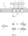
- Figure 1 illustrates a longitudinal section of a connection arrangement according to an exemplary embodiment of the invention.
- the connection arrangement is basically used to connect two connection partners, for example a component and a stack, or two PCBs.
- the pair of both connection partners can comprise the connection arrangement.
- connection arrangement can be part of component carrier structure which comprises at least one of a panel, an array, a component carrier, and an arrangement of a component carrier and a component 5.
- the component carrier can comprise at least one component 5 being surface mounted on and/or embedded in the component carrier, wherein the at least one component is in particular selected from a group consisting of an electronic component, an electrically non-conductive and/or electrically conductive inlay, a heat transfer unit, a light guiding element, an energy harvesting unit, an active electronic component, a passive electronic component, an electronic chip, a storage device, a filter, an integrated circuit, a signal processing component, a power management component, an optoelectronic interface element, a voltage converter, a cryptographic component, a transmitter and/or receiver, an electromechanical transducer, an actuator, a hermetic device, a microelectromechanical system, a microprocessor, a capacitor, a resistor, an inductance, an accumulator, a switch, a camera, an antenna, a magnetic element, a further component carrier, and a logic chip.
- the at least one component is in particular selected from a group consisting of an electronic component, an electrically
- the component carrier can comprise a stack 6 comprising at least one electrically conductive layer structure and/or at least one electrically insulating layer structure, and the connection arrangement.
- At least one of the electrically conductive layer structures of the component carrier can comprise at least one of the group consisting of copper, aluminum, nickel, silver, gold, palladium, titanium, and tungsten, any of the mentioned materials being optionally coated with supra-conductive material such as graphene.
- the electrically insulating layer structure can comprise at least one of the group consisting of resin, in particular reinforced or non-reinforced resin, for instance epoxy resin or Bismaleimide-Triazine resin, FR-4, FR-5, cyanate ester, polyphenylene derivate, glass, prepreg material, polyimide, polyamide, liquid crystal polymer, epoxy-based build-up film, polytetrafluoroethylene, a ceramic, and a metal oxide.
- resin in particular reinforced or non-reinforced resin, for instance epoxy resin or Bismaleimide-Triazine resin, FR-4, FR-5, cyanate ester, polyphenylene derivate, glass, prepreg material, polyimide, polyamide, liquid crystal polymer, epoxy-based build-up film, polytetrafluoroethylene, a ceramic, and a metal oxide.
- the component carrier can be shaped as a plate.
- the component carrier can be configured as one of the group consisting of a printed circuit board, a substrate, and an interposer.
- the component carrier can be configured as a laminate-type component carrier.
- connection arrangement comprises (in this embodiment three) first electrically conductive connection elements 1 and (in this embodiment three) second electrically conductive connection elements 2.
- the first connection elements 1 and the second connection elements 2 are configured such that, upon connecting the first connection elements 1 with the second connection elements 2 along a connection direction z, a form fit is directly established between a pair of one of the first connection elements 1 and the corresponding second connection element 2 that limits or even inhibits a relative motion between the first connection element 1 and the second connection element 2 of the pair in a plane perpendicular to the connection direction z.
- At least the second connection elements 2 can be formed of copper by a conventional electroplating process.
- the second connection elements 2 each have a concave connection surface 22 with a dimple which is at least partially filled by a solderable material 4.
- solderable material 4 soft solders and alloys of copper, silver, zinc, tin, or lead with optional additives of bismuth, indium, cadmium can be used. Also brazing alloys for example of brass or nickel silver are conceivable.
- the solderable material 4 can be deposited by any method such as sputtering.
- the use of the dimples further enables the use of a larger amount of solderable material 4 compared with connection surfaces without dimples.
- the larger amount of solderable material 4 in turn enables larger distances to be bridged between the first and second connection elements 1, 2 in the connection direction z.
- the pillar formed by the first connection element 1 should have a complementary convex shape to enhance the centering process.
- the convex and concave shapes of the connection surfaces 21, 22 of the first and second connection elements 1, 2 can thus be used as a support for centering the component 5 with respect to the stack 6 before or during soldering.
- the dimple can be used to assist cohesion forces to center the component 5; this especially applies for a relative light component 5.
- a relative heavy component 5 When a relative heavy component 5 is used, the same can be centered under vibration support such as sound-supported soldering. The centering can take place when the solderable material 4 becomes liquid. As a result, a soldering is achieved without blowholes, and a surface in a connection region can be sealed without cracks, pores etc.
- the first connection elements 1 each form a part, for example a terminal, a pad or a contact, of the component 5 to be embedded or surface mounted in or on the stack 6 of layer structures, and the second connection elements 2 are formed in an interior of the stack 6.
- the second connection elements 2 can protrude in the connection direction z from the main surface of the stack 6 of the component carrier structure, or they can be formed at or on a main surface of the stack 6.
- the term "main surface” designates that surface where terminals or contacts are arranged or that surface which extends perpendicular to a direction in which the conductive and insulating layers are superposed (layered) on each other.
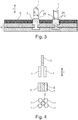
- Figure 2 illustrates different cross-sectional views of first and second connection elements 1, 2 according to exemplary embodiments of the invention.
- the first connection element 1 has a circular cross-section, whereas in the lower middle of Figure 2 , the first connection element 1 has a non-circular cross-section.
- a contact surface between the first and second connection elements 1, 2 is enlarged with the first connection element 1 having the non-circular cross-section.
- the non-circular cross-sections can have an oval, elliptic or any other non-circular shape. Due to the non-circular cross-sections, the registration tolerances can be enlarged. The accuracy in a contacting process can also be increased.
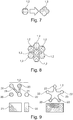
- FIG. 3 illustrates a longitudinal section of a connection arrangement according to an exemplary embodiment of the invention.
- Each first connection element 1 has a first cooperating surface 11, and each second connection element 2 has a second cooperating surface 12.
- the first and second cooperating surfaces 11, 21 cooperate and engage with each other.
- the cooperating surfaces 11, 21 of the connection elements 1, 2 are configured for promoting centering of the connection elements 1, 2 upon their connection.
- the first and second cooperating surfaces 11, 21 have complementary shapes.
- the cooperating surface 11, 21 of one of the first and the second connection elements 1, 2 has a concave shape and the cooperating surface 11, 21 of the other one of the first and the second connection elements 1, 2 has a complementary convex shape in the cross section perpendicular to the connection direction z.
- the second connection elements 2 can be formed of copper by a conventional electroplating process.
- Each second connection element 2 has a shape of a pillar or of an elevated land which protrudes from a solder mask 8, which is provided as an uppermost layer on the stack 6.
- the cooperating surfaces 11, 21 are provided.
- the centering of the first and second connection elements 1, 2 and thus between the connection partners is improved.
- Figure 4 illustrates a longitudinal section and a cross section of a connection arrangement according to an exemplary embodiment of the invention.
- the top longitudinal view depicts the connection arrangement before soldering, and the lower longitudinal view depicts the connection arrangement after soldering.
- a plurality of first connection elements 1 and one second connection element 2 establish an electric contact and a mechanical contact both in the connection direction z and in a direction perpendicular to the connection direction z.
- the second connection element 2 is guided by the first connection elements 1 along the connection direction z during connecting the first connection elements 1 with the second connection element 2.
- the first connection element 1 is composed of multiple spaced bodies 1 delimiting an accommodation volume for receiving and accommodating the second connection element 2.
- the embodiment of Figure 4 uses a key-lock function, and the first and second connection elements 1, 2 can have a shape of conical cylinders or pillars.
- the pillars can be placed in such a way that the key-lock function is enabled. It is advantageous if the pillar(s) of at least one of the first and second connection elements 1, 2 has (have) a conical design so that a good centering property is achieved.
- connection by means of the key-lock function can also achieved by other connection elements except for the pillars.
- Figure 5 illustrates a cross-sectional view and longitudinal sections of a connection arrangement according to an exemplary embodiment of the invention.
- the longitudinal view at the top right position depicts the connection arrangement before soldering, and the longitudinal view at the lower left position depicts the connection arrangement after soldering.
- the embodiment of Figure 5 is similar to the embodiment of Figure 4 , except for the first and second connection elements 1, 2 which are coated with solderable material 7.
- solderable material 7 soft solders and alloys of copper, silver, zinc, tin, or lead with optional additives of bismuth, indium, cadmium can be used. Also brazing alloys for example of brass or nickel silver are conceivable.
- the solderable material 7 can be deposited by any method such as sputtering, electroless tin plating or electrolytic deposition of a tin/sliver alloy.
- coated copper pillars enable a very reliable key lock connection because a relatively large surface is soldered.
- a use of smaller solder layers can result in a reduction of a short-circuit bond between connection points. It is to be noted that a connection by means of the key-lock function can also achieved by other coated connection elements except for the pillars.
- Figure 6 illustrates longitudinal sections of a connection arrangement according to an exemplary embodiment of the invention.
- the connection arrangement is provided to connect two component carriers 9, 10 to each other, which are for example two printed circuit boards (PCB).
- Each component carrier 9, 10 comprises a stack 6 having at least one electrically conductive layer structure and/or at least one electrically insulating layer structure, a solder mask 8 at an outermost connection surface of each stack 6, and the connection arrangement in and/or on each stack 6.
- connection arrangement comprises first and second connection elements 1, 2 which are formed as vias in the respective electrically conductive layer structure of the stacks 6.
- the connection arrangement further comprises a third connection element 3 arranged in the connection direction z between the first connection element 1 and the second connection element 2 for accomplishing a form fit both between the first and third connection elements 1, 3 and between the second and third connection elements 2, 3.
- a form fit is thus indirectly formed between the first and second connection elements 1, 2, whereas, in contrast thereto, the form fit in the embodiments of Figures 1 and 3 is rather directly formed between the first and second connection elements 1, 2.
- the third connection element 3 is made of or comprises a soldering material and has a convex shape. If the third connection element 3 is a solder ball with a copper core, a defined distance between the component carriers 9, 10 can be set.
- the first and second connection elements 1, 2 each have a land with a cooperating surface 11, 21 which is configured for promoting centering of the connection elements 1, 2, 3 upon their connection.
- the cooperating surfaces 11, 21 of the first and second connection elements 1, 2 each have a concave shape in a cross section perpendicular to the connection direction, which corresponds to the complementary convex shape of the third connection element 3.
- larger distances in the connection direction z can be bridged between the connection partners.
- the first and second connection elements 1, 2 formed as vias can be used as a centering aid when connecting both component carriers 9, 10.
- the solder masks 8 can be used to create a centering aid for the lands having the concave cooperating surfaces 11, 21.
- Figure 7 illustrates cross-sectional views of connection elements according to exemplary embodiments of the invention.
- the connection element 1, 2 has a circular cross-section
- the connection element 1, 2 at the right side of Figure 7 has a non-circular cross-section.
- the cross section of the connection element 1, 2 at the right side of Figure 7 is composed by regularly arranging (in this embodiment four) circular cross sections around a central circular cross section.
- the cross section of the connection element 1, 2 at the right side of Figure 7 is blossom-shaped or shamrock-shaped.
- connection element 1, 2 has an alveolar-shaped, honeycomb-shaped or hexagonal cross section. Furthermore, a plurality of connection elements 1, 2 are arranged adjacent to each other. Due to the hexagonal or honeycomb-shaped cross sections, the highest packing density of the connection elements 1, 2 can be achieved. The edges of the alveolar-shaped, honeycomb-shaped or hexagonal cross section can be rounded.
- Figure 9 illustrates cross-sectional views and longitudinal sections of connection elements according to exemplary embodiments of the invention.
- connection element 1, 2 At the left upper side of Figure 9 , a cross section of a connection element 1, 2 is shown, and at the left lower side of Figure 9 , a front view of the connection element 1, 2 is shown.
- the connection element 1,2 at the left side of Figure 9 is composed of a plurality of circular or non-circular pillars 20. Some of the pillars are interconnected by elongated lands 21.
- connection element 1, 2 At the right upper side of Figure 9 , a cross section of a connection element 1, 2 is shown, and at the right lower side of Figure 9 , a front view of the connection element 1, 2 is shown.
- the connection element 1, 2 at the right side of Figure 9 is composed of a star-shaped basis element 23. At each tip of the star-shaped basis element 23, a circular or non-circular pillar 22 is arranged.
- the elongated lands 21 and the star-shaped basis element 23, which interconnect the pillars 20 and 22, respectively, can have a contribution to a reduction in the number of rewiring layers.
- connection elements 1, 2 Due to the non-circular cross sections of the connection elements 1, 2 in the embodiments of Figures 2 and 7-9 , the mechanical strength, in particular the buckling strength and the section modulus can be improved even when the surface area is equivalent to a circular cross section. Due to a larger circumference, skin effects (i.e. an increased resistance of current-carrying conductors at high frequencies) can be reduced.
- connection elements 1, 2, 3 can be a pillar, in particular a copper pillar, a via, a land, a solder ball or a ball comprising a central non-solderable body coated with solderable material 7.
- the pillar can be a conical pillar.
- the connection joints can include two or more pillars. Ideally, three pillars are preferred in view of the mechanical reliability.
- the copper pillar can be built-up on a copper plate, on a copper pad or on a copper foil.
- the copper pillar can be connected to the copper plate or pad by pressing and spot welding.
- the copper pillar can otherwise be connected by compression bonding or ultrasonic bonding.
- the copper pillar can have a tolerance of 6 ⁇ m or less.
- the copper pillar can also be deposited by a galvanic process on the copper foil, pad or plate.
- connection elements 1, 2 (for example the pillars) can have an aspect ratio between the length and a largest or main diameter of more than 1, preferably of more than 2, more preferred more than 3.
- first and second connection elements 1, 2 can be connected by sound-supported soldering.
Landscapes
- Engineering & Computer Science (AREA)
- Microelectronics & Electronic Packaging (AREA)
- Manufacturing & Machinery (AREA)
- Ceramic Engineering (AREA)
- Physics & Mathematics (AREA)
- Geometry (AREA)
- Combinations Of Printed Boards (AREA)
- Structures For Mounting Electric Components On Printed Circuit Boards (AREA)
- Electric Connection Of Electric Components To Printed Circuits (AREA)
Abstract
Description
- The invention relates to a connection arrangement, a component carrier and a method of forming a component carrier structure.
- A conventional component carrier comprises a stack having at least one electrically conductive layer structure and at least one electrically insulating layer structure, and component and a connection arrangement to connect the component to the stack. For example, the connection arrangement is formed by pads of the component and vias of the stack, wherein the pads are electrically connected to the vias, for example by soldering.
- It is an object of the invention to provide a connection arrangement, a component carrier and a method of forming a component carrier structure, by which a centering between two connection partners, which are to be connected by the connection arrangement, is enhanced and higher package densities can be achieved. This object is achieved by the subject matters of the independent claims.
- According to an exemplary embodiment of the invention, a connection arrangement comprises a first electrically conductive connection element and a second electrically conductive connection element. The first connection element and the second connection element are configured such that, upon connecting the first connection element with the second connection element along a connection direction, a form fit is (directly or indirectly) established between the first connection element and the second connection element that limits (or even inhibits) a relative motion between the first connection element and the second connection element in a plane perpendicular to the connection direction.
- According to another exemplary embodiment of the invention, a component carrier comprises a stack comprising at least one electrically conductive layer structure and/or at least one electrically insulating layer structure, and the connection arrangement in and/or on the stack.
- According to another exemplary embodiment of the invention, a method of forming a component carrier structure comprises connecting a first electrically conductive connection element with a second electrically conductive connection element along a connection direction in such a way that (a direct or indirect) form fit is established between the first connection element and the second connection element that limits (or even inhibits) motion of the first connection element and the second connection element relative to each other in a plane perpendicular to the connection direction.
- The form fit is usually achieved before soldering and enables a more accurate centering of both connection partners before soldering.
- In the following, further exemplary embodiments of the present invention will be explained.
- In an embodiment, the connection arrangement further comprises a third connection element arranged in the connection direction between the first connection element and the second connection element for accomplishing a form fit both between the first and third connection elements and between the second and third connection elements. The third connection element can be a copper ball which is coated by a coating material.
- In an embodiment, a cross-section of at least one of the first connection element and the second connection element has a non-circular cross-section, for example oval, elliptic, rectangular, triangular, star-shaped, blossom-shaped, shamrock-shaped, a alveolar-shaped, honeycomb-shaped, etc. The non-circular cross-section of the first and/or second connection elements, which can be an elevated land or a pillar, allow more accurate connections and high packing densities. Due to the non-circular cross-sections, the registration tolerances can be enlarged. The accuracy in a contacting process can be increased.
- Furthermore, due to the non-circular cross section of the connection element, the mechanical strength, in particular the buckling strength and the section modulus can be improved. Due to a larger circumference of the connection element, skin effects (i.e. an increased resistance of current-carrying conductors at high frequencies) can be reduced.
- In an embodiment, cooperating surfaces of the connection elements are configured for promoting centering of the connection elements upon their connection, wherein in particular a cooperating surface of one of the first and the second connection elements has a concave shape and a cooperating surface of the other one of the first and the second connection elements has a complementary convex shape in a cross section perpendicular to the connection direction. The convex and concave shapes of the cooperating surfaces of the first and second connection elements can thus be used as a support for centering a connection partner such as a component with respect to another connection partner such as a stack during soldering.
- In an embodiment, at least one of the connection elements has a concave connection surface with a dimple which is preferably at least partially filled by a solderable material. As the solderable material, soft solders and alloys of copper, silver, zinc, tin, or lead with optional additives of bismuth, indium, cadmium can be used. Also brazing alloys for example of brass or nickel silver are conceivable. The solderable material can be deposited by any method such as sputtering. The use of the dimple enables the use of a larger amount of solderable material compared with a connection surface without dimple. The larger amount of solderable material in turn enables larger distances to be bridged between the first and second connection partners in the connection direction. The dimple can also be used to support cohesion forces to center a connection partner such as a component with respect to another connection partner such as a stack. This especially applies for a relative light component. When a relative heavy component is used, the same can be centered under vibration support such as sound-supported soldering. The centering can take place when the solderable material becomes liquid. As a result, a soldering can be obtained without blowholes, and a surface in a connection region can be sealed without cracks, pores etc.
- In an embodiment, the first connection element and the second connection element establish an electric contact and a mechanical contact both in the connection direction and in a direction perpendicular to the connection direction, i.e. one of the first connection element and the second connection element can be guided by the other one of the first connection element and the second connection element along the connection direction during connecting the first connection element with the second connection element before soldering. The first connection element can be composed of multiple spaced bodies delimiting an accommodation volume for receiving and accommodating the second connection element. Thereby, a key-lock function can be achieved. It is advantageous if conical pillars are used so that a good centering property is achieved.
- In an embodiment, at least one of the connection elements is a pillar, in particular a copper pillar, a via, a land, a solder ball or a ball comprising a central non-solderable body coated with solderable material. As the solderable material, soft solders and alloys of copper, silver, zinc, tin, or lead with optional additives of bismuth, indium, cadmium can be used. Also brazing alloys for example of brass or nickel silver are conceivable. The solderable material can be deposited by any method such as sputtering. On the one hand, such coated connection elements enable a very reliable connection because a relative large surface is soldered. On the other hand, a use of smaller solder layers can result in a reduction of a short-circuit bond between connection points.
- The pillar can be a conical pillar. The connection joints can include two or more pillars. Ideally, three pillars are preferred in view of the mechanical reliability. A copper pillar can be built-up on a copper plate, on a copper pad or on a copper foil. The copper pillar can be connected to the copper plate or pad by pressing and spot welding. The copper pillar can otherwise be connected by compression bonding or ultrasonic bonding. The copper pillar can have a tolerance of 6 µm or less. The copper pillar can also be deposited on the copper foil, pad or plate by a galvanic process.
- In an embodiment, one of the first and second connection elements forms a part, for example a terminal, a pad or a contact, of a component to be embedded or surface mounted in or on a stack of layer structures, and the other one of the first and second connection elements is formed in an interior of the stack or preferably at a main surface of the stack. The other one of the first and second connection elements can protrude in the connection direction from the main surface of the stack of a component carrier structure.
- In all embodiments of the present invention, the connection elements (for example the pillars) can have an aspect ratio between the length and a largest or main diameter of more than 1, preferably of more than 2, more preferred more than 3.
- In an embodiment of the component carrier structure, the same comprises at least one of a panel, an array, a component carrier, and an arrangement of a component carrier and the component.
- In an embodiment of the method, the first and second connection elements are connected by sound-supported soldering. As the solderable material, soft solders and alloys of copper, silver, zinc, tin, or lead with optional additives of bismuth, indium, cadmium can be used. Also brazing alloys for example of brass or nickel silver are conceivable. The solderable material can be deposited by any method such as sputtering.
- In the context of the present application, the term "component carrier" may particularly denote any support structure which is capable of accommodating one or more components thereon and/or therein for providing mechanical support and/or electrical connectivity. In other words, a component carrier may be configured as a mechanical and/or electronic carrier for components. In particular, a component carrier may be one of a printed circuit board, an organic interposer, and an IC (integrated circuit) substrate. A component carrier may also be a hybrid board combining different ones of the above mentioned types of component carriers.
- In an embodiment, the component carrier comprises a stack of at least one electrically insulating layer structure and at least one electrically conductive layer structure. For example, the component carrier may be a laminate of the mentioned electrically insulating layer structure(s) and electrically conductive layer structure(s), in particular formed by applying mechanical pressure and/or thermal energy. The mentioned stack may provide a plate-shaped component carrier capable of providing a large mounting surface for further components and being nevertheless very thin and compact. The term "layer structure" may particularly denote a continuous layer, a patterned layer or a plurality of nonconsecutive islands within a common plane.
- In an embodiment, the component carrier is shaped as a plate. This contributes to the compact design, wherein the component carrier nevertheless provides a large basis for mounting components thereon. Furthermore, in particular a naked die as example for an embedded electronic component, can be conveniently embedded, thanks to its small thickness, into a thin plate such as a printed circuit board.
- In an embodiment, the component carrier is configured as one of the group consisting of a printed circuit board, a substrate (in particular an IC substrate), and an interposer.
- In the context of the present application, the term "printed circuit board" (PCB) may particularly denote a plate-shaped component carrier which is formed by laminating several electrically conductive layer structures with several electrically insulating layer structures, for instance by applying pressure and/or by the supply of thermal energy. As preferred materials for PCB technology, the electrically conductive layer structures are made of copper, whereas the electrically insulating layer structures may comprise resin and/or glass fibers, so-called prepreg or prefabricated copper claded core materials or FR4 material. The various electrically conductive layer structures may be connected to one another in a desired way by forming through-holes through the laminate, for instance by laser drilling or mechanical drilling, and by filling them with electrically conductive material (in particular copper), thereby forming vias as through-hole connections. Apart from one or more components which may be embedded in a printed circuit board, a printed circuit board is usually configured for accommodating one or more components on one or both opposing surfaces of the plate-shaped printed circuit board. They may be connected to the respective main surface by soldering. A dielectric part of a PCB may be composed of resin with reinforcing fibers (such as glass fibers).
- In the context of the present application, the term "substrate" may particularly denote a small component carrier having substantially the same size as a component (in particular an electronic component) to be mounted thereon. More specifically, a substrate can be understood as a carrier for electrical connections or electrical networks as well as component carrier comparable to a printed circuit board (PCB), however with a considerably higher density of laterally and/or vertically arranged connections. Lateral connections are for example conductive paths, whereas vertical connections may be for example drill holes. These lateral and/or vertical connections are arranged within the substrate and can be used to provide electrical, thermal and/or mechanical connections of housed components or unhoused components (such as bare dies), particularly of IC chips, with a printed circuit board or intermediate printed circuit board. Thus, the term "substrate" also includes "IC substrates". A dielectric part of a substrate may be composed of resin with reinforcing particles (such as reinforcing spheres, in particular glass spheres).
- The substrate or interposer may comprise or consist of at least a layer of glass, silicon (Si) or a photoimageable or dry-etchable organic material like epoxy-based build-up material (such as epoxy-based build-up film) or polymer compounds like polyimide, polybenzoxazole, or benzocyclobutene.
- In an embodiment, the at least one electrically insulating layer structure comprises at least one of the group consisting of resin (such as reinforced or non-reinforced resins, for instance epoxy resin or Bismaleimide-Triazine resin), cyanate ester, polyphenylene derivate, glass (in particular glass fibers, multilayer glass, glass-like materials), prepreg material (such as FR-4 or FR-5), polyimide, polyamide, liquid crystal polymer (LCP), epoxy-based build-up film, polytetrafluoroethylene (Teflon), a ceramic, and a metal oxide. Reinforcing materials such as webs, fibers or spheres, for example made of glass (multilayer glass) may be used as well. Although prepreg particularly FR4 are usually preferred for rigid PCBs, other materials in particular epoxy-based build-up film or photoimageable dielectric material may be used as well. For high frequency applications, high-frequency materials such as polytetrafluoroethylene, liquid crystal polymer and/or cyanate ester resins, low temperature cofired ceramics (LTCC) or other low, very low or ultra-low DK materials may be implemented in the component carrier as electrically insulating layer structure.
- In an embodiment, the at least one electrically conductive layer structure comprises at least one of the group consisting of copper, aluminum, nickel, silver, gold, palladium, titanium and tungsten. Although copper is usually preferred, other materials or coated versions thereof are possible as well, in particular coated with supra-conductive material such as graphene.
- The at least one component can be selected from a group consisting of an electrically non-conductive inlay, an electrically conductive inlay (such as a metal inlay, preferably comprising copper or aluminum), a heat transfer unit (for example a heat pipe), a light guiding element (for example an optical waveguide or a light conductor connection), an electronic component, or combinations thereof. For example, the component can be an active electronic component, a passive electronic component, an electronic chip, a storage device (for instance a DRAM or another data memory), a filter, an integrated circuit, a signal processing component, a power management component, an optoelectronic interface element, a light emitting diode, a photocoupler, a voltage converter (for example a DC/DC converter or an AC/DC converter), a cryptographic component, a transmitter and/or receiver, an electromechanical transducer, a sensor, an actuator, a microelectromechanical system (MEMS), a microprocessor, a capacitor, a resistor, an inductance, a battery, a switch, a camera, an antenna, a logic chip, and an energy harvesting unit and a hermetic package. However, other components may be embedded in the component carrier. For example, a magnetic element can be used as a component. Such a magnetic element may be a permanent magnetic element (such as a ferromagnetic element, an antiferromagnetic element, a multiferroic element or a ferrimagnetic element, for instance a ferrite core) or may be a paramagnetic element. However, the component may also be a substrate, an interposer or a further component carrier, for example in a board-in-board configuration. The component may be surface mounted on the component carrier and/or may be embedded in an interior thereof. Moreover, also other components, in particular those which generate and emit electromagnetic radiation and/or are sensitive with regard to electromagnetic radiation propagating from an environment, may be used as component.
- In an embodiment, the component carrier is a laminate-type component carrier. In such an embodiment, the component carrier is a compound of multiple layer structures which are stacked and connected together by applying a pressing force and/or heat.
- After processing interior layer structures of the component carrier, it is possible to cover (in particular by lamination) one or both opposing main surfaces of the processed layer structures symmetrically or asymmetrically with one or more further electrically insulating layer structures and/or electrically conductive layer structures. In other words, a build-up may be continued until a desired number of layers is obtained.
- After having completed formation of a stack of electrically insulating layer structures and electrically conductive layer structures, it is possible to proceed with a surface treatment of the obtained layers structures or component carrier.
- In particular, an electrically insulating solder resist may be applied to one or both opposing main surfaces of the layer stack or component carrier in terms of surface treatment. For instance, it is possible to form such as solder resist on an entire main surface and to subsequently pattern the layer of solder resist so as to expose one or more electrically conductive surface portions which shall be used for electrically coupling the component carrier to an electronic periphery. The surface portions of the component carrier remaining covered with solder resist may be efficiently protected against oxidation or corrosion, in particular surface portions containing copper.
- It is also possible to apply a surface finish selectively to exposed electrically conductive surface portions of the component carrier in terms of surface treatment. Such a surface finish may be an electrically conductive cover material on exposed electrically conductive layer structures (such as pads, conductive tracks, etc., in particular comprising or consisting of copper) on a surface of a component carrier. If such exposed electrically conductive layer structures are left unprotected, then the exposed electrically conductive component carrier material (in particular copper) might oxidize, making the component carrier less reliable. A surface finish may then be formed for instance as an interface between a surface mounted component and the component carrier. The surface finish has the function to protect the exposed electrically conductive layer structures (in particular copper circuitry) and enable a joining process with one or more components, for instance by soldering. Examples for appropriate materials for a surface finish are OSP (Organic Solderability Preservative), Electroless Nickel Immersion Gold (ENIG), gold (in particular Hard Gold), chemical tin, nickel-gold, nickel-palladium, etc.
- The aspects defined above and further aspects of the invention are apparent from the examples of embodiment to be described hereinafter and are explained with reference to these examples of embodiment.
-
Figure 1 illustrates a longitudinal section of a connection arrangement according to an exemplary embodiment of the invention. -
Figure 2 illustrates different cross-sectional views of first and second connection elements according to exemplary embodiments of the invention. -
Figure 3 illustrates a longitudinal section of a connection arrangement according to an exemplary embodiment of the invention. -
Figure 4 illustrates a longitudinal section and a cross section of a connection arrangement according to an exemplary embodiment of the invention. -
Figure 5 illustrates cross-sectional views and longitudinal sections of a connection arrangement according to an exemplary embodiment of the invention. -
Figure 6 illustrates longitudinal sections of a connection arrangement according to an exemplary embodiment of the invention. -
Figure 7 illustrates cross-sectional views of connection elements according to exemplary embodiments of the invention. -
Figure 8 illustrates a cross-sectional view of connection elements according to an exemplary embodiment of the invention. -
Figure 9 illustrates cross-sectional views and longitudinal sections of connection elements according to exemplary embodiments of the invention. - The illustrations in the drawings are schematic. In different drawings, similar or identical elements are provided with the same reference signs.
-
Figure 1 illustrates a longitudinal section of a connection arrangement according to an exemplary embodiment of the invention. The connection arrangement is basically used to connect two connection partners, for example a component and a stack, or two PCBs. The pair of both connection partners can comprise the connection arrangement. - The connection arrangement can be part of component carrier structure which comprises at least one of a panel, an array, a component carrier, and an arrangement of a component carrier and a
component 5. - The component carrier can comprise at least one
component 5 being surface mounted on and/or embedded in the component carrier, wherein the at least one component is in particular selected from a group consisting of an electronic component, an electrically non-conductive and/or electrically conductive inlay, a heat transfer unit, a light guiding element, an energy harvesting unit, an active electronic component, a passive electronic component, an electronic chip, a storage device, a filter, an integrated circuit, a signal processing component, a power management component, an optoelectronic interface element, a voltage converter, a cryptographic component, a transmitter and/or receiver, an electromechanical transducer, an actuator, a hermetic device, a microelectromechanical system, a microprocessor, a capacitor, a resistor, an inductance, an accumulator, a switch, a camera, an antenna, a magnetic element, a further component carrier, and a logic chip. - The component carrier can comprise a
stack 6 comprising at least one electrically conductive layer structure and/or at least one electrically insulating layer structure, and the connection arrangement. - At least one of the electrically conductive layer structures of the component carrier can comprise at least one of the group consisting of copper, aluminum, nickel, silver, gold, palladium, titanium, and tungsten, any of the mentioned materials being optionally coated with supra-conductive material such as graphene.
- The electrically insulating layer structure can comprise at least one of the group consisting of resin, in particular reinforced or non-reinforced resin, for instance epoxy resin or Bismaleimide-Triazine resin, FR-4, FR-5, cyanate ester, polyphenylene derivate, glass, prepreg material, polyimide, polyamide, liquid crystal polymer, epoxy-based build-up film, polytetrafluoroethylene, a ceramic, and a metal oxide.
- The component carrier can be shaped as a plate. The component carrier can be configured as one of the group consisting of a printed circuit board, a substrate, and an interposer. The component carrier can be configured as a laminate-type component carrier.
- The connection arrangement comprises (in this embodiment three) first electrically
conductive connection elements 1 and (in this embodiment three) second electricallyconductive connection elements 2. Thefirst connection elements 1 and thesecond connection elements 2 are configured such that, upon connecting thefirst connection elements 1 with thesecond connection elements 2 along a connection direction z, a form fit is directly established between a pair of one of thefirst connection elements 1 and the correspondingsecond connection element 2 that limits or even inhibits a relative motion between thefirst connection element 1 and thesecond connection element 2 of the pair in a plane perpendicular to the connection direction z. - At least the
second connection elements 2 can be formed of copper by a conventional electroplating process. - In this embodiment, the
second connection elements 2 each have aconcave connection surface 22 with a dimple which is at least partially filled by asolderable material 4. As thesolderable material 4, soft solders and alloys of copper, silver, zinc, tin, or lead with optional additives of bismuth, indium, cadmium can be used. Also brazing alloys for example of brass or nickel silver are conceivable. Thesolderable material 4 can be deposited by any method such as sputtering. By producing theconcave connection surface 22 of thesecond connection elements 2 with the dimple, the same can be used for centering and contacting a matchingfirst connection element 1 which are copper pillars in this embodiment. The use of the dimples further enables the use of a larger amount ofsolderable material 4 compared with connection surfaces without dimples. The larger amount ofsolderable material 4 in turn enables larger distances to be bridged between the first andsecond connection elements first connection element 1 should have a complementary convex shape to enhance the centering process. The convex and concave shapes of the connection surfaces 21, 22 of the first andsecond connection elements component 5 with respect to thestack 6 before or during soldering. The dimple can be used to assist cohesion forces to center thecomponent 5; this especially applies for arelative light component 5. When a relativeheavy component 5 is used, the same can be centered under vibration support such as sound-supported soldering. The centering can take place when thesolderable material 4 becomes liquid. As a result, a soldering is achieved without blowholes, and a surface in a connection region can be sealed without cracks, pores etc. - The
first connection elements 1 each form a part, for example a terminal, a pad or a contact, of thecomponent 5 to be embedded or surface mounted in or on thestack 6 of layer structures, and thesecond connection elements 2 are formed in an interior of thestack 6. - Alternatively, instead of being formed in the interior of the
stack 6, thesecond connection elements 2 can protrude in the connection direction z from the main surface of thestack 6 of the component carrier structure, or they can be formed at or on a main surface of thestack 6. In the context of the present invention, the term "main surface" designates that surface where terminals or contacts are arranged or that surface which extends perpendicular to a direction in which the conductive and insulating layers are superposed (layered) on each other. -
Figure 2 illustrates different cross-sectional views of first andsecond connection elements - At the left side of
Figure 2 , a cross section of thesecond connection element 2 is shown, which has a non-circular cross-section. - In the upper middle of
Figure 2 , thefirst connection element 1 has a circular cross-section, whereas in the lower middle ofFigure 2 , thefirst connection element 1 has a non-circular cross-section. As can be taken from the right side ofFigure 2 , a contact surface between the first andsecond connection elements first connection element 1 having the non-circular cross-section. - The non-circular cross-sections can have an oval, elliptic or any other non-circular shape. Due to the non-circular cross-sections, the registration tolerances can be enlarged. The accuracy in a contacting process can also be increased.
-
Figure 3 illustrates a longitudinal section of a connection arrangement according to an exemplary embodiment of the invention. Eachfirst connection element 1 has a first cooperatingsurface 11, and eachsecond connection element 2 has a second cooperating surface 12. During connecting the first andsecond connection elements connection elements connection elements - The first and second cooperating surfaces 11, 21 have complementary shapes. In more detail, the cooperating
surface second connection elements surface second connection elements - The
second connection elements 2 can be formed of copper by a conventional electroplating process. Eachsecond connection element 2 has a shape of a pillar or of an elevated land which protrudes from asolder mask 8, which is provided as an uppermost layer on thestack 6. At the top of each pillar or elevated land, the cooperating surfaces 11, 21 are provided. - For example, by the complementary (convex or concave) shapes of the cooperating surfaces 21, 22 of the first and
second connection elements second connection elements -
Figure 4 illustrates a longitudinal section and a cross section of a connection arrangement according to an exemplary embodiment of the invention. The top longitudinal view depicts the connection arrangement before soldering, and the lower longitudinal view depicts the connection arrangement after soldering. - A plurality of
first connection elements 1 and onesecond connection element 2 establish an electric contact and a mechanical contact both in the connection direction z and in a direction perpendicular to the connection direction z. In more detail, thesecond connection element 2 is guided by thefirst connection elements 1 along the connection direction z during connecting thefirst connection elements 1 with thesecond connection element 2. - The
first connection element 1 is composed of multiple spacedbodies 1 delimiting an accommodation volume for receiving and accommodating thesecond connection element 2. - The embodiment of
Figure 4 uses a key-lock function, and the first andsecond connection elements second connection elements - It is to be noted that a connection by means of the key-lock function can also achieved by other connection elements except for the pillars.
-
Figure 5 illustrates a cross-sectional view and longitudinal sections of a connection arrangement according to an exemplary embodiment of the invention. The longitudinal view at the top right position depicts the connection arrangement before soldering, and the longitudinal view at the lower left position depicts the connection arrangement after soldering. - The embodiment of
Figure 5 is similar to the embodiment ofFigure 4 , except for the first andsecond connection elements solderable material 7. As thesolderable material 7, soft solders and alloys of copper, silver, zinc, tin, or lead with optional additives of bismuth, indium, cadmium can be used. Also brazing alloys for example of brass or nickel silver are conceivable. Thesolderable material 7 can be deposited by any method such as sputtering, electroless tin plating or electrolytic deposition of a tin/sliver alloy. On the one hand, such coated copper pillars enable a very reliable key lock connection because a relatively large surface is soldered. On the other hand, a use of smaller solder layers can result in a reduction of a short-circuit bond between connection points. It is to be noted that a connection by means of the key-lock function can also achieved by other coated connection elements except for the pillars. -
Figure 6 illustrates longitudinal sections of a connection arrangement according to an exemplary embodiment of the invention. In this embodiment, the connection arrangement is provided to connect twocomponent carriers component carrier stack 6 having at least one electrically conductive layer structure and/or at least one electrically insulating layer structure, asolder mask 8 at an outermost connection surface of eachstack 6, and the connection arrangement in and/or on eachstack 6. - The connection arrangement comprises first and
second connection elements stacks 6. The connection arrangement further comprises athird connection element 3 arranged in the connection direction z between thefirst connection element 1 and thesecond connection element 2 for accomplishing a form fit both between the first andthird connection elements third connection elements Figure 6 , a form fit is thus indirectly formed between the first andsecond connection elements Figures 1 and3 is rather directly formed between the first andsecond connection elements - The
third connection element 3 is made of or comprises a soldering material and has a convex shape. If thethird connection element 3 is a solder ball with a copper core, a defined distance between thecomponent carriers - The first and
second connection elements surface connection elements second connection elements third connection element 3. Thus, there are dimples in the cooperating surfaces 11, 21, which allow the use of a larger volume of soldering material. At the same time, larger distances in the connection direction z can be bridged between the connection partners. - The first and
second connection elements component carriers surfaces -
Figure 7 illustrates cross-sectional views of connection elements according to exemplary embodiments of the invention. At the left side ofFigure 7 , theconnection element connection element Figure 7 has a non-circular cross-section. In more detail, the cross section of theconnection element Figure 7 is composed by regularly arranging (in this embodiment four) circular cross sections around a central circular cross section. Thus, the cross section of theconnection element Figure 7 is blossom-shaped or shamrock-shaped. -
Figure 8 illustrates a cross-sectional view of connection elements according to an exemplary embodiment of the invention. Eachconnection element connection elements connection elements -
Figure 9 illustrates cross-sectional views and longitudinal sections of connection elements according to exemplary embodiments of the invention. - At the left upper side of
Figure 9 , a cross section of aconnection element Figure 9 , a front view of theconnection element connection element Figure 9 is composed of a plurality of circular ornon-circular pillars 20. Some of the pillars are interconnected byelongated lands 21. - At the right upper side of
Figure 9 , a cross section of aconnection element Figure 9 , a front view of theconnection element connection element Figure 9 is composed of a star-shapedbasis element 23. At each tip of the star-shapedbasis element 23, a circular ornon-circular pillar 22 is arranged. - The elongated lands 21 and the star-shaped
basis element 23, which interconnect thepillars - Due to the non-circular cross sections of the
connection elements Figures 2 and7-9 , the mechanical strength, in particular the buckling strength and the section modulus can be improved even when the surface area is equivalent to a circular cross section. Due to a larger circumference, skin effects (i.e. an increased resistance of current-carrying conductors at high frequencies) can be reduced. - In all embodiments of the present invention, at least one of the
connection elements solderable material 7. The pillar can be a conical pillar. The connection joints can include two or more pillars. Ideally, three pillars are preferred in view of the mechanical reliability. - The copper pillar can be built-up on a copper plate, on a copper pad or on a copper foil. The copper pillar can be connected to the copper plate or pad by pressing and spot welding. The copper pillar can otherwise be connected by compression bonding or ultrasonic bonding. The copper pillar can have a tolerance of 6 µm or less. The copper pillar can also be deposited by a galvanic process on the copper foil, pad or plate.
- In all embodiments of the present invention, the
connection elements 1, 2 (for example the pillars) can have an aspect ratio between the length and a largest or main diameter of more than 1, preferably of more than 2, more preferred more than 3. - Generally, the first and
second connection elements - It should be noted that the term "comprising" does not exclude other elements or steps and the "a" or "an" does not exclude a plurality. Also elements described in association with different embodiments may be combined.
- It should also be noted that reference signs in the claims shall not be construed as limiting the scope of the claims.
- Implementation of the invention is not limited to the preferred embodiments shown in the figures and described above. Instead, a multiplicity of variants are possible which use the solutions shown and the principle according to the invention even in the case of fundamentally different embodiments.
Claims (15)
- A connection arrangement for forming a component carrier structure, wherein the connection arrangement comprises:a first electrically conductive connection element (1); anda second electrically conductive connection element (2);wherein the first connection element (1) and the second connection element (2) are configured such that, upon connecting the first connection element (1) with the second connection element (2) along a connection direction (z), a form fit is established between the first connection element (1) and the second connection element (2) that limits a relative motion between the first connection element (1) and the second connection element (2) in a plane perpendicular to the connection direction (z).
- The connection arrangement according to the preceding claim,
further comprising a third connection element (3) arranged in the connection direction (z) between the first connection element (1) and the second connection element (2) for accomplishing a form fit both between the first and third connection elements (1, 3) and between the second and third connection elements (2, 3). - The connection arrangement according to any one of the preceding claims,
wherein a cross-section of at least one of the first connection element (1) and the second connection element (2) has a non-circular cross-section. - The connection arrangement according to any one of the preceding claims,
wherein cooperating surfaces (11, 21) of the connection elements (1, 2, 3) are configured for promoting centering of the connection elements (1, 2, 3) upon their connection, wherein in particular a cooperating surface (11, 21) of one of the first and the second connection elements (1, 2) has a concave shape and a cooperating surface (11, 21) of the other one of the first and the second connection elements (1, 2) has a complementary convex shape. - The connection arrangement according to any one of the preceding claims,
wherein at least one of the connection elements (1, 2) has a concave connection surface (22) with a dimple which is preferably at least partially filled by a solderable material (4). - The connection arrangement according to any one of the preceding claims,
wherein the first connection element (1) and the second connection element (2) establish an electric contact and a mechanical contact both in the connection direction (z) and in a direction perpendicular to the connection direction (z). - The connection arrangement according to the preceding claim,
wherein the first connection element (1) is composed of multiple spaced bodies delimiting an accommodation volume for receiving and accommodating the second connection element (2). - The connection arrangement according to any one of the preceding claims,
wherein at least one of the connection elements (1, 2, 3) is a pillar, in particular a copper pillar, a via, a land, a solder ball or a ball comprising a central non-solderable body coated with solderable material (7). - The connection arrangement according to any one of the preceding claims,
wherein one of the first and second connection elements (1, 2) forms a part of a component (5) to be embedded or surface mounted in or on a stack (6) of layer structures, and the other one of the first and second connection elements (1, 2) is formed in an interior of the stack (6) or at a main surface of the stack (6). - The connection arrangement according to the preceding claim,
wherein the other one of the first and second connection elements (1, 2) protrudes in the connection direction (z) from the main surface of the stack (6) of a component carrier structure. - The connection arrangement according to the preceding claim,
wherein the component carrier structure comprises at least one of a panel, an array, a component carrier, and an arrangement of a component carrier and the component (5). - A component carrier (9, 10), wherein the component carrier comprises:a stack (6) comprising at least one electrically conductive layer structure and/or at least one electrically insulating layer structure;a connection arrangement according to any of claims 1 to 11 in and/or on the stack (6).
- The component carrier (9, 10) according to claim 12, comprising at least one of the following features:the component carrier (9, 10) comprises at least one component (5) being surface mounted on and/or embedded in the component carrier (9, 10), wherein the at least one component is in particular selected from a group consisting of an electronic component, an electrically non-conductive and/or electrically conductive inlay, a heat transfer unit, a light guiding element, an energy harvesting unit, an active electronic component, a passive electronic component, an electronic chip, a storage device, a filter, an integrated circuit, a signal processing component, a power management component, an optoelectronic interface element, a voltage converter, a cryptographic component, a transmitter and/or receiver, an electromechanical transducer, an actuator, a microelectromechanical system, a microprocessor, a capacitor, a resistor, an inductance, an accumulator, a switch, a camera, an antenna, a magnetic element, a further component carrier (9, 10), and a logic chip;wherein at least one of the electrically conductive layer structures of the component carrier (9, 10) comprises at least one of the group consisting of copper, aluminum, nickel, silver, gold, palladium, and tungsten, any of the mentioned materials being optionally coated with supra-conductive material such as graphene;wherein the electrically insulating layer structure comprises at least one of the group consisting of resin, in particular reinforced or non-reinforced resin, for instance epoxy resin or Bismaleimide-Triazine resin, FR-4, FR-5, cyanate ester, polyphenylene derivate, glass, prepreg material, polyimide, polyamide, liquid crystal polymer, epoxy-based build-up film, polytetrafluoroethylene, a ceramic, and a metal oxide;wherein the component carrier (9, 10) is shaped as a plate;wherein the component carrier (9, 10) is configured as one of the group consisting of a printed circuit board, a substrate, and an interposer;wherein the component carrier (9, 10) is configured as a laminate-type component carrier.
- A method of forming a component carrier structure, wherein the method comprises connecting a first electrically conductive connection element (1) with a second electrically conductive connection element (2) along a connection direction (z) in such a way that a form fit is established between the first connection element (1) and the second connection element (2) that limits motion of the first connection element (1) and the second connection element (2) relative to each other in a plane perpendicular to the connection direction (z).
- The method according to the preceding claim,
wherein the first and second connection elements (1, 2) are connected by sound-supported soldering.
Priority Applications (3)
| Application Number | Priority Date | Filing Date | Title |
|---|---|---|---|
| EP19196363.6A EP3793336A1 (en) | 2019-09-10 | 2019-09-10 | Connection arrangement, component carrier and method of forming a component carrier structure |
| US16/947,786 US11658142B2 (en) | 2019-09-10 | 2020-08-17 | Connection arrangement, component carrier and method of forming a component carrier structure |
| CN202010917844.8A CN112563788A (en) | 2019-09-10 | 2020-09-03 | Connecting device, component carrier and method for forming a component carrier structure |
Applications Claiming Priority (1)
| Application Number | Priority Date | Filing Date | Title |
|---|---|---|---|
| EP19196363.6A EP3793336A1 (en) | 2019-09-10 | 2019-09-10 | Connection arrangement, component carrier and method of forming a component carrier structure |
Publications (1)
| Publication Number | Publication Date |
|---|---|
| EP3793336A1 true EP3793336A1 (en) | 2021-03-17 |
Family
ID=67953545
Family Applications (1)
| Application Number | Title | Priority Date | Filing Date |
|---|---|---|---|
| EP19196363.6A Ceased EP3793336A1 (en) | 2019-09-10 | 2019-09-10 | Connection arrangement, component carrier and method of forming a component carrier structure |
Country Status (3)
| Country | Link |
|---|---|
| US (1) | US11658142B2 (en) |
| EP (1) | EP3793336A1 (en) |
| CN (1) | CN112563788A (en) |
Families Citing this family (3)
| Publication number | Priority date | Publication date | Assignee | Title |
|---|---|---|---|---|
| CN113517209A (en) * | 2020-04-10 | 2021-10-19 | 长鑫存储技术有限公司 | Semiconductor structure and method of forming the same |
| KR102919381B1 (en) | 2021-07-28 | 2026-01-28 | 삼성전자주식회사 | Semiconductor Package |
| US12315999B2 (en) * | 2022-07-15 | 2025-05-27 | Aptiv Technologies AG | Solderable waveguide antenna |
Citations (4)
| Publication number | Priority date | Publication date | Assignee | Title |
|---|---|---|---|---|
| US20030146518A1 (en) * | 1999-02-24 | 2003-08-07 | Junichi Hikita | Semiconductor device of chip-on-chip structure, assembling process therefor, and semiconductor chip to be bonded to solid surface |
| US20050173795A1 (en) * | 2004-02-05 | 2005-08-11 | Hodson Kenneth G. | Socket grid array |
| US20080203138A1 (en) * | 2007-02-28 | 2008-08-28 | Fujitsu Limited | Method of mounting an electronic component and mounting apparatus |
| US20160293565A1 (en) * | 2015-04-06 | 2016-10-06 | SK Hynix Inc. | Semiconductor packages with socket plug interconnection structures |
Family Cites Families (10)
| Publication number | Priority date | Publication date | Assignee | Title |
|---|---|---|---|---|
| JP3808030B2 (en) * | 2002-11-28 | 2006-08-09 | 沖電気工業株式会社 | Semiconductor device and manufacturing method thereof |
| US7015590B2 (en) | 2003-01-10 | 2006-03-21 | Samsung Electronics Co., Ltd. | Reinforced solder bump structure and method for forming a reinforced solder bump |
| US6989586B2 (en) | 2003-03-31 | 2006-01-24 | Intel Corporation | Integrated circuit packages with reduced stress on die and associated substrates, assemblies, and systems |
| KR20060105382A (en) | 2005-04-04 | 2006-10-11 | 엘지전자 주식회사 | Bonded Structure of PCB and its method |
| WO2009084770A1 (en) * | 2007-12-28 | 2009-07-09 | Phicom Corporation | Contact tip structure of a connecting element |
| CN102224584A (en) | 2008-11-25 | 2011-10-19 | 住友电木株式会社 | Electronic component package and electronic component package manufacturing method |
| JP2014179518A (en) | 2013-03-15 | 2014-09-25 | Dainippon Printing Co Ltd | Multilayer wiring board and component mounting multilayer wiring board |
| DE102017113094A1 (en) * | 2017-06-14 | 2018-12-20 | Osram Opto Semiconductors Gmbh | Method for self-aligned loading of a connection carrier with a component, device and optoelectronic component |
| CN109729639B (en) | 2018-12-24 | 2020-11-20 | 奥特斯科技(重庆)有限公司 | Component carrier including pillars on a coreless substrate |
| EP3739618A1 (en) * | 2019-05-15 | 2020-11-18 | AT & S Austria Technologie & Systemtechnik Aktiengesellschaft | Component carrier with surface-contactable component embedded in laminated stack |
-
2019
- 2019-09-10 EP EP19196363.6A patent/EP3793336A1/en not_active Ceased
-
2020
- 2020-08-17 US US16/947,786 patent/US11658142B2/en active Active
- 2020-09-03 CN CN202010917844.8A patent/CN112563788A/en active Pending
Patent Citations (4)
| Publication number | Priority date | Publication date | Assignee | Title |
|---|---|---|---|---|
| US20030146518A1 (en) * | 1999-02-24 | 2003-08-07 | Junichi Hikita | Semiconductor device of chip-on-chip structure, assembling process therefor, and semiconductor chip to be bonded to solid surface |
| US20050173795A1 (en) * | 2004-02-05 | 2005-08-11 | Hodson Kenneth G. | Socket grid array |
| US20080203138A1 (en) * | 2007-02-28 | 2008-08-28 | Fujitsu Limited | Method of mounting an electronic component and mounting apparatus |
| US20160293565A1 (en) * | 2015-04-06 | 2016-10-06 | SK Hynix Inc. | Semiconductor packages with socket plug interconnection structures |
Also Published As
| Publication number | Publication date |
|---|---|
| US11658142B2 (en) | 2023-05-23 |
| CN112563788A (en) | 2021-03-26 |
| US20210074662A1 (en) | 2021-03-11 |
Similar Documents
| Publication | Publication Date | Title |
|---|---|---|
| EP3547361B1 (en) | Component carrier connected with tilted other component carrier for short electric connection | |
| US11810844B2 (en) | Component carrier and method of manufacturing the same | |
| CN111511105B (en) | Component carrier with through-holes filled with additional plated structures and bridge structures | |
| EP1868422B1 (en) | Electronic component built-in substrate and method of manufacturing the same | |
| US11470714B2 (en) | Component carrier with embedded component and horizontally elongated via | |
| EP3836209B1 (en) | Component carrier and method of manufacturing the same | |
| US11700690B2 (en) | Component carrier with blind hole filled with an electrically conductive medium and fulfilling a minimum thickness design rule | |
| US11324122B2 (en) | Component carrier and method of manufacturing the same | |
| US11658142B2 (en) | Connection arrangement, component carrier and method of forming a component carrier structure | |
| EP4170712A2 (en) | Electronic assembly and electronic system with impedance matched interconnect structures | |
| CN212727898U (en) | component carrier | |
| JP2008270532A (en) | Inductor built-in substrate and manufacturing method thereof | |
| EP3840020A2 (en) | Component carrier having a double dielectric layer and method of manufacturing the same | |
| CN115190693A (en) | Component carrier and method for producing the same | |
| US11551989B2 (en) | Component carrier and method of manufacturing the same | |
| EP3846598A1 (en) | Arrangement with a central carrier and two opposing layer stacks, component carrier and manufacturing method | |
| CN112447659B (en) | Component carrier and method for producing a component carrier | |
| EP3349553A1 (en) | Component carrier with pad covered by surface finish-solder structure | |
| CN113937072A (en) | Component carrier and method for producing the same | |
| US20240021440A1 (en) | Component Carrier and Method of Manufacturing the Same | |
| US12219701B2 (en) | Component carrier | |
| CN211320082U (en) | Component carrier | |
| KR101551177B1 (en) | Embedded printed circuit board with rewiring layer and method of manufacturing the same | |
| CN120529490A (en) | A method for manufacturing a carrier board, a power module, a power module assembly method, and a magnetic component |
Legal Events
| Date | Code | Title | Description |
|---|---|---|---|
| PUAI | Public reference made under article 153(3) epc to a published international application that has entered the european phase |
Free format text: ORIGINAL CODE: 0009012 |
|
| STAA | Information on the status of an ep patent application or granted ep patent |
Free format text: STATUS: THE APPLICATION HAS BEEN PUBLISHED |
|
| AK | Designated contracting states |
Kind code of ref document: A1 Designated state(s): AL AT BE BG CH CY CZ DE DK EE ES FI FR GB GR HR HU IE IS IT LI LT LU LV MC MK MT NL NO PL PT RO RS SE SI SK SM TR |
|
| AX | Request for extension of the european patent |
Extension state: BA ME |
|
| STAA | Information on the status of an ep patent application or granted ep patent |
Free format text: STATUS: REQUEST FOR EXAMINATION WAS MADE |
|
| 17P | Request for examination filed |
Effective date: 20210913 |
|
| RBV | Designated contracting states (corrected) |
Designated state(s): AL AT BE BG CH CY CZ DE DK EE ES FI FR GB GR HR HU IE IS IT LI LT LU LV MC MK MT NL NO PL PT RO RS SE SI SK SM TR |
|
| STAA | Information on the status of an ep patent application or granted ep patent |
Free format text: STATUS: EXAMINATION IS IN PROGRESS |
|
| 17Q | First examination report despatched |
Effective date: 20221007 |
|
| STAA | Information on the status of an ep patent application or granted ep patent |
Free format text: STATUS: THE APPLICATION HAS BEEN REFUSED |
|
| 18R | Application refused |
Effective date: 20251024 |