EP3790150B1 - Apparatus and method for battery module balancing - Google Patents
Apparatus and method for battery module balancing Download PDFInfo
- Publication number
- EP3790150B1 EP3790150B1 EP19873876.7A EP19873876A EP3790150B1 EP 3790150 B1 EP3790150 B1 EP 3790150B1 EP 19873876 A EP19873876 A EP 19873876A EP 3790150 B1 EP3790150 B1 EP 3790150B1
- Authority
- EP
- European Patent Office
- Prior art keywords
- battery module
- path
- battery
- connection
- cell assembly
- Prior art date
- Legal status (The legal status is an assumption and is not a legal conclusion. Google has not performed a legal analysis and makes no representation as to the accuracy of the status listed.)
- Active
Links
Images


Classifications
-
- H—ELECTRICITY
- H02—GENERATION; CONVERSION OR DISTRIBUTION OF ELECTRIC POWER
- H02J—ELECTRIC POWER NETWORKS; CIRCUIT ARRANGEMENTS OR SYSTEMS FOR SUPPLYING OR DISTRIBUTING ELECTRIC POWER; SYSTEMS FOR STORING ELECTRIC ENERGY
- H02J7/00—Circuit arrangements for charging or discharging batteries or for supplying loads from batteries
- H02J7/50—Circuit arrangements for charging or discharging batteries or for supplying loads from batteries acting upon multiple batteries simultaneously or sequentially
- H02J7/52—Circuit arrangements for charging or discharging batteries or for supplying loads from batteries acting upon multiple batteries simultaneously or sequentially for charge balancing, e.g. equalisation of charge between batteries
- H02J7/56—Active balancing, e.g. using capacitor-based, inductor-based or DC-DC converters
-
- H—ELECTRICITY
- H02—GENERATION; CONVERSION OR DISTRIBUTION OF ELECTRIC POWER
- H02J—ELECTRIC POWER NETWORKS; CIRCUIT ARRANGEMENTS OR SYSTEMS FOR SUPPLYING OR DISTRIBUTING ELECTRIC POWER; SYSTEMS FOR STORING ELECTRIC ENERGY
- H02J7/00—Circuit arrangements for charging or discharging batteries or for supplying loads from batteries
- H02J7/50—Circuit arrangements for charging or discharging batteries or for supplying loads from batteries acting upon multiple batteries simultaneously or sequentially
- H02J7/52—Circuit arrangements for charging or discharging batteries or for supplying loads from batteries acting upon multiple batteries simultaneously or sequentially for charge balancing, e.g. equalisation of charge between batteries
- H02J7/54—Passive balancing, e.g. using resistors or parallel MOSFETs
-
- H—ELECTRICITY
- H01—ELECTRIC ELEMENTS
- H01M—PROCESSES OR MEANS, e.g. BATTERIES, FOR THE DIRECT CONVERSION OF CHEMICAL ENERGY INTO ELECTRICAL ENERGY
- H01M10/00—Secondary cells; Manufacture thereof
- H01M10/42—Methods or arrangements for servicing or maintenance of secondary cells or secondary half-cells
- H01M10/425—Structural combination with electronic components, e.g. electronic circuits integrated to the outside of the casing
-
- H—ELECTRICITY
- H01—ELECTRIC ELEMENTS
- H01M—PROCESSES OR MEANS, e.g. BATTERIES, FOR THE DIRECT CONVERSION OF CHEMICAL ENERGY INTO ELECTRICAL ENERGY
- H01M10/00—Secondary cells; Manufacture thereof
- H01M10/42—Methods or arrangements for servicing or maintenance of secondary cells or secondary half-cells
- H01M10/48—Accumulators combined with arrangements for measuring, testing or indicating the condition of cells, e.g. the level or density of the electrolyte
- H01M10/482—Accumulators combined with arrangements for measuring, testing or indicating the condition of cells, e.g. the level or density of the electrolyte for several batteries or cells simultaneously or sequentially
-
- H—ELECTRICITY
- H02—GENERATION; CONVERSION OR DISTRIBUTION OF ELECTRIC POWER
- H02J—ELECTRIC POWER NETWORKS; CIRCUIT ARRANGEMENTS OR SYSTEMS FOR SUPPLYING OR DISTRIBUTING ELECTRIC POWER; SYSTEMS FOR STORING ELECTRIC ENERGY
- H02J7/00—Circuit arrangements for charging or discharging batteries or for supplying loads from batteries
- H02J7/80—Circuit arrangements for charging or discharging batteries or for supplying loads from batteries including monitoring or indicating arrangements
-
- H—ELECTRICITY
- H01—ELECTRIC ELEMENTS
- H01M—PROCESSES OR MEANS, e.g. BATTERIES, FOR THE DIRECT CONVERSION OF CHEMICAL ENERGY INTO ELECTRICAL ENERGY
- H01M10/00—Secondary cells; Manufacture thereof
- H01M10/05—Accumulators with non-aqueous electrolyte
- H01M10/052—Li-accumulators
-
- H—ELECTRICITY
- H01—ELECTRIC ELEMENTS
- H01M—PROCESSES OR MEANS, e.g. BATTERIES, FOR THE DIRECT CONVERSION OF CHEMICAL ENERGY INTO ELECTRICAL ENERGY
- H01M10/00—Secondary cells; Manufacture thereof
- H01M10/42—Methods or arrangements for servicing or maintenance of secondary cells or secondary half-cells
- H01M10/425—Structural combination with electronic components, e.g. electronic circuits integrated to the outside of the casing
- H01M2010/4271—Battery management systems including electronic circuits, e.g. control of current or voltage to keep battery in healthy state, cell balancing
-
- H—ELECTRICITY
- H01—ELECTRIC ELEMENTS
- H01M—PROCESSES OR MEANS, e.g. BATTERIES, FOR THE DIRECT CONVERSION OF CHEMICAL ENERGY INTO ELECTRICAL ENERGY
- H01M10/00—Secondary cells; Manufacture thereof
- H01M10/42—Methods or arrangements for servicing or maintenance of secondary cells or secondary half-cells
- H01M10/425—Structural combination with electronic components, e.g. electronic circuits integrated to the outside of the casing
- H01M2010/4278—Systems for data transfer from batteries, e.g. transfer of battery parameters to a controller, data transferred between battery controller and main controller
-
- H—ELECTRICITY
- H02—GENERATION; CONVERSION OR DISTRIBUTION OF ELECTRIC POWER
- H02J—ELECTRIC POWER NETWORKS; CIRCUIT ARRANGEMENTS OR SYSTEMS FOR SUPPLYING OR DISTRIBUTING ELECTRIC POWER; SYSTEMS FOR STORING ELECTRIC ENERGY
- H02J2207/00—Details of circuit arrangements for charging or discharging batteries or supplying loads from batteries
- H02J2207/20—Charging or discharging characterised by the power electronics converter
-
- Y—GENERAL TAGGING OF NEW TECHNOLOGICAL DEVELOPMENTS; GENERAL TAGGING OF CROSS-SECTIONAL TECHNOLOGIES SPANNING OVER SEVERAL SECTIONS OF THE IPC; TECHNICAL SUBJECTS COVERED BY FORMER USPC CROSS-REFERENCE ART COLLECTIONS [XRACs] AND DIGESTS
- Y02—TECHNOLOGIES OR APPLICATIONS FOR MITIGATION OR ADAPTATION AGAINST CLIMATE CHANGE
- Y02E—REDUCTION OF GREENHOUSE GAS [GHG] EMISSIONS, RELATED TO ENERGY GENERATION, TRANSMISSION OR DISTRIBUTION
- Y02E60/00—Enabling technologies; Technologies with a potential or indirect contribution to GHG emissions mitigation
- Y02E60/10—Energy storage using batteries
Definitions
- the present disclosure relates to an apparatus and method for battery module balancing, and more particularly, to an apparatus and method for battery module balancing capable of effectively equalizing charges of battery modules while balancing a plurality of battery modules included in a battery pack.
- Secondary batteries commercially available at present include nickel-cadmium batteries, nickel-hydrogen batteries, nickel-zinc batteries, lithium secondary batteries and the like.
- the lithium secondary batteries have almost no memory effect compared to nickel-based secondary batteries and thus are in the limelight due to advantageous such as free charging and discharging, low self-discharge rate and high energy density.
- Batteries are used in a wide variety of applications, and large capacities are often required for devices such as electric-driven vehicles or smart grid systems to which batteries are frequently utilized.
- the capacity of the secondary battery namely the capacity of a battery cell itself, may be increased.
- the capacity increase effect is not large and there is a physical limitation on the size expansion of the secondary battery.
- a battery pack in which a plurality of battery modules are connected in series and in parallel is widely used.
- the plurality of battery modules included in the battery pack have different capacity performances from each other due to the difference in intrinsic characteristics or manufacturing environments and versatility of system applications as the use time elapses, which causes a difference in terminal voltage or state of charge (SOC) of the corresponding modules due to charging and discharging.
- SOC state of charge
- a specific battery module having degraded performance may limit the charging or discharging capacity of the entire battery pack, age the battery pack and cause problems such as overvoltage.
- module balancing Evenly controlling the terminal voltages between battery modules is known as module balancing or inter-module charge equalization.
- inter-module charge equalization it is difficult to individually perform balancing between specific battery modules that require module balancing, among a plurality of battery modules.
- a circuit structure becomes complicated, and the number and volume of wiring bundles increase.
- it is not easy to manufacture a module equalization device and the manufacturing process may take long time and suffer from a high defective rate.
- the present disclosure is designed to solve the problems of the related art, and therefore the present disclosure is directed to providing an apparatus and method for battery module balancing, which may effectively equalize charges between battery modules while balancing a plurality of battery modules included in a battery pack.
- an apparatus for battery module balancing balances a plurality of battery modules that respectively include cell assemblies having at least one secondary battery and electrically connected in series
- the apparatus for battery module balancing comprising: a monitoring unit provided to each battery module and configured to monitor at least one of voltage, temperature and current of each cell assembly; a self-circulating path provided to each battery module and electrically connected to both ends of each cell assembly to form a closed circuit, the self-circulating path having an inductor configured to allow a charging and discharging current to flow on the self-circulating path and a first discharge MOSFET configured to open or close the self-circulating path: a connector provided to each battery module and configured to have a plurality of connection terminals; a connection path provided to each battery module to electrically connect both ends of the inductor to the plurality of connection terminals and electrically connect neighboring battery modules to each other through the plurality of connection terminals, the connection path having a second discharge MOSFET provided on the connection path to
- the processor may be configured to repeatedly turn on and off the first discharge MOSFET or the second discharge MOSFET so that charges of neighboring cell assemblies are equalized through the self-circulating path and the connection path.
- the processor may be configured to repeatedly turn on and off the first discharge MOSFET to generate an induced electromotive force with respect to the inductor by means of a discharging current of the cell assembly flowing through the self-circulating path and transmit the generated induced electromotive force to a neighboring battery module through the connection path.
- the processor may be configured to repeatedly turn on and off the second discharge MOSFET to generate an induced electromotive force of the inductor by means of a discharging current of the cell assembly flowing through the connection path and transmit the generated induced electromotive force to a neighboring battery module through the self-circulating path.
- connection path includes a first internal connection path and a second internal connection path
- the plurality of connection terminals may include a first connection terminal and a second connection terminal
- the first internal connection path may be configured to electrically connect a node between a positive electrode terminal of each cell assembly and one end of the inductor directly to the first connection terminal
- the second internal connection path may be configured to electrically connect a node between the other end of the inductor and the first discharge MOSFET directly to the second connection terminal.
- the second discharge MOSFET may be configured to be provided on the second internal connection path.
- connection path may further include an external connection path configured to electrically connect the first connection terminal and the second connection terminal of each battery module directly to the second connection terminal and the first connection terminal of a neighboring battery module, respectively.
- a battery management system according to an embodiment of the present disclosure comprises the apparatus for battery module balancing according to the present disclosure.
- a battery pack according to an embodiment of the present disclosure comprises the apparatus for battery module balancing according to the present disclosure.
- a method for battery module balancing balances a plurality of battery modules that respectively include cell assemblies having at least one secondary battery and electrically connected in series, the method for battery module balancing comprising: monitoring at least one of voltage, temperature and current of each cell assembly; and receiving a state of each cell assembly, which is monitored in the monitoring step, and controlling opening and closing operations of a first discharge MOSFET configured to open or close a self-circulating path, which is electrically connected to both ends of each cell assembly to form a closed circuit and has an inductor configured to allow a charging and discharging current to flow on the self-circulating path, and a second discharge MOSFET configured to open or close a connection path, which electrically connects both ends of the inductor to a plurality of connection terminals and electrically connects neighboring battery modules to each other through the plurality of connection terminals, on the basis of the received state of each cell assembly so that the plurality of battery modules are balanced.
- the battery module equalization device has an advantage of simplifying the charge equalization circuit by easily transferring energy between the battery modules without an external power connection.
- the present disclosure may have various effects other than the above, and other effects of the present disclosure may be understood from the following description and more clearly figured out by the embodiments of the present disclosure.
- processor refers to a unit that processes at least one function or operation, and may be implemented by hardware, software, or a combination of hardware and software.
- the secondary battery refers to a one independent cell that includes a negative electrode terminal and a positive electrode terminal and is physically separable.
- one pouch-type lithium polymer cell may be regarded as the secondary battery.
- An apparatus for battery module balancing according to an embodiment of the present disclosure may be an apparatus for balancing a plurality of battery modules 100, 200 included in a battery pack. More specifically, the apparatus for battery module balancing according to an embodiment of the present disclosure may be an apparatus for equalizing charges between a plurality of battery modules 100, 200, which respectively include cell assemblies 10, 20 having at least one secondary battery and electrically connected with each other in series.
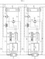
- FIG. 1 is a diagram schematically showing some components of an apparatus for battery module balancing according to an embodiment of the present disclosure.
- the apparatus for battery module balancing includes monitoring units 110, 210, a self-circulating path L1, connectors 120, 220, connection paths L2, L3 and processors 130, 230.
- the monitoring units 110, 210 may be provided to the battery modules 100, 200, respectively.
- the monitoring units 110, 210 may be electrically connected to the cell assemblies 10, 20 provided in the battery modules 100, 200, respectively.
- the monitoring units 110, 210 may be electrically connected to both ends of the cell assemblies 10, 20, respectively.
- the monitoring units 110, 210 may be electrically connected to both ends of a current sensor provided on a charging and discharging path, respectively.
- the monitoring units 110, 210 may be configured to monitor at least one of voltage, temperature and current of each cell assembly 10, 20.
- the monitoring units 110, 210 may be configured to measure at least one of voltage, temperature and current of the secondary battery included in each cell assembly 10, 20.
- the monitoring units 110, 210 may be configured to measure the voltage of the secondary battery.
- the monitoring units 110, 210 may be electrically connected to both ends of the cell assemblies 10, 20.
- the monitoring units 110, 210 may be electrically connected to the processors 130, 230 to transmit and receive electric signals.
- the monitoring units 110, 210 may be electrically connected to the processors 130, 230 to transmit and receive electric signals.
- the monitoring units 110, 210 may measure the voltage at both ends of the cell assemblies 10, 20 at time intervals and output a signal indicating the magnitude of the measured voltage to the processors 130, 230.
- the processors 130, 230 may determine the voltage of the cell assemblies 10, 20 from the signal output from the monitoring units 110, 210.
- the monitoring units 110, 210 may be implemented using a voltage measurement circuit commonly used in the art.
- the monitoring units 110, 210 may be configured to measure the current flowing through the cell assemblies 10, 20.
- the monitoring units 110, 210 may be electrically connected to both ends of a current sensor provided on the charging and discharging path of the cell assemblies 10, 20.
- the monitoring units 110, 210 may be electrically coupled to the processors 130, 230 to transmit and receive electric signals.
- the monitoring units 110, 210 may repeatedly measure the magnitude of the charging current or the discharging current of the cell assemblies 10, 20 at time intervals and output a signal indicating the magnitude of the measured current to the processors 130, 230.
- the processors 130, 230 may determine the magnitude of the current from the signal output from the monitoring units 110, 210.
- the current sensor may be implemented using a hall sensor or a sense resistor generally used in the art.
- the monitoring units 110, 210 may be configured to measure the temperature of the cell assemblies 10, 20.
- the monitoring units 110, 210 may be connected to the cell assemblies 10, 20 to measure the temperature of the secondary battery included in the cell assemblies 10, 20.
- the monitoring units 110, 210 may be electrically coupled to the processors 130, 230 to transmit and receive electric signals.
- the monitoring units 110, 210 may repeatedly measure the temperatures of the cell assemblies 10, 20 at time intervals and output a signal indicating the magnitude of the measured temperature to the processors 130, 230.
- the processors 130, 230 may determine the temperature of the secondary battery from the signal output from the monitoring units 110, 210.
- monitoring units 110, 210 may be implemented using a thermocouple commonly used in the art.
- the self-circulating path L1 may be provided to each battery module 100, 200.
- the self-circulating path L1 may be electrically connected to both ends of each cell assembly 10, 20 to form a closed circuit.
- the self-circulating path L1 may be provided to each battery module 100, 200 and electrically connected to both ends of the cell assemblies 10, 20, respectively.
- the self-circulating path L1 may form an electrically closed circuit extending from the positive electrode terminals of the cell assemblies 10, 20 to the negative electrode terminals of the cell assemblies 10, 20.
- the self-circulating path L1 may include inductors 151, 251 and first discharge MOSFETs 152, 252 on the self-circulating path L1.
- the inductors 151, 251 may be configured to allow a charging and discharging current to flow on the path.
- the inductors 151, 251 may be provided on the self-circulating path L1.
- the inductors 151, 251 may be provided on the self-circulating path L1 that is directly connected to the positive electrode terminals of the cell assemblies 10, 20.
- the inductors 151, 251 may be configured to allow a charging and discharging current flowing on the self-circulating path L1 to flow therethrough.
- the inductors 151, 251 may be implemented using a coil having an inductance L[H] component according to Faraday's law.
- the first discharge MOSFETs 152, 252 may be configured to open and close the path.
- the first discharge MOSFETs 152, 252 may be provided on the self-circulating path L1 to open and close the self-circulating path L1.
- the first discharge MOSFETs 152, 252 may be directly provided between the inductors 151, 251 and the negative electrode terminals of the cell assemblies 10, 20.
- the first discharge MOSFETs 152, 252 may be electrically connected to the processors 130, 230 to transmit and receive electric signals so as to be turned off or on under the control of the processors 130, 230.
- the connectors 120, 220 may be provided to the battery modules 100, 200, respectively.
- the connectors 120, 220 may be provided at one side of the battery modules 100, 200, respectively.
- the connectors 120, 220 may include a plurality of connection terminals.
- the connectors 120, 220 may include two connection terminals.
- the connectors 120, 220 may electrically connect the battery modules 100, 200 to each other directly through the connection terminals.
- connection paths L2, L3 may be provided to the battery modules 100, 200, respectively.
- the connection paths L2, L3 may electrically connect both ends of the inductors 151, 251 to the plurality of connection terminals 121, 122, 221, 222, respectively.
- the connection paths L2, L3 may electrically connect neighboring battery modules 100, 200 to each other through the plurality of connection terminals 121, 122, 221, 222.
- the connection paths L2, L3 may be provided to the battery modules 100, 200, respectively, to electrically connect both ends of the inductors 151, 251 directly to the connection terminals 121, 122, 221, 222.
- the connection paths L2, L3 may electrically connect the connection terminals 121, 122, 221, 222 respectively provided to the battery modules 100, 200 to each other such that neighboring battery modules 100, 200 are electrically connected.
- connection paths L2, L3 may include second discharge MOSFETs 161, 261, respectively.
- the second discharge MOSFETs 161, 261 may be provided on the path to open and close the path.
- the second discharge MOSFETs 161, 261 may be provided on the connection paths L2, L3 to open and close the connection paths L2, L3.
- the second discharge MOSFETs 161, 261 may be provided between the inductors 151, 251 and the connection terminals 121, 122, 221, 222.
- the second discharge MOSFETs 161, 261 may be electrically connected to the processors 130, 230 to transmit and receive electric signals so as to be turned off or on under the control of the processors 130, 230.
- the first discharge MOSFETs 152, 252 and the second discharge MOSFETs 161, 261 are a field effect transistor (FET) element having a gate terminal, a drain terminal and a source terminal and may be turned on or off depending on whether a channel is formed according to a voltage applied between the gate terminal and the source terminal.
- FET field effect transistor
- the FET element may be a metal oxide semiconductor field effect transistor (MOSFET).
- first discharge MOSFETs 152, 252 and the second discharge MOSFETs 161, 261 may include a FET body and a parasitic diode, respectively.
- the parasitic diode is a diode connected in parallel with the FET body and acts as a rectifier for conducting a current in one direction.
- the drain terminal may be directly connected to one end of the inductors 151, 251, and the source terminal may be directly connected to the negative electrode terminal of the cell assemblies 10, 20.
- the parasitic diodes may allow a current to be conducted from the source terminal to the drain terminal. That is, the parasitic diodes of the first discharge MOSFETs 152, 252 may set the direction from the negative electrode terminals of the cell assemblies 10, 20 to the inductors 151, 251 as a forward direction.
- the drain terminal may be directly connected to the connection terminals 121, 221, and the source terminal may be directly connected to one end of the inductors 151, 251.
- the parasitic diodes may allow a current to be conducted from the source terminal to the drain terminal. That is, the parasitic diodes of the second discharge MOSFETs 161, 261 may set the direction from the inductors 151, 251 to the connection terminals 121, 221 as a forward direction.
- the processors 130, 230 may control the turn-on and turn-off operations of the first discharge MOSFETs 152, 252 and the second discharge MOSFETs 161, 261.
- the processors 130, 230 may be electrically connected to the gate terminals of the first discharge MOSFETs 152, 252 and the second discharge MOSFETs 161, 261 to transmit and receive electric signals.
- the processors 130, 230 may control the turn-on and turn-off operations of the first discharge MOSFETs 152, 252 and the second discharge MOSFETs 161, 261 by controlling the voltages applied to the gate terminals of the first discharge MOSFETs 152, 252 and the second discharge MOSFETs 161, 261.
- connection paths L2, L3 may include a first internal connection path L2 and a second internal connection path L2.
- the plurality of connection terminals 121, 122, 221, 222 may include first connection terminals 122, 222 and second connection terminals 121, 221.
- the first internal connection path L2 may be configured to electrically connect a node between the positive electrode terminal of each cell assembly 10, 20 and one end of the inductors 151, 251 directly to the first connection terminals 122, 222.
- the second internal connection path L2 may be configured to electrically connect a node between the other end of the inductors 151, 251 and the first discharge MOSFETs 152, 252 directly to the second connection terminals 121, 221.
- the second discharge MOSFETs 161, 261 may be provided on the second internal connection path L2.
- the second discharge MOSFETs 161, 261 may be provided on the second internal connection path L2 that directly connects the node between the other end of the inductors 151, 251 and the first discharge MOSFETs 152, 252 directly to the second connection terminal 121, 221.
- connection paths L2, L3 may further include an external connection path L3.
- the external connection path L3 may be configured to be electrically connect the first connection terminals 122, 222 and the second connection terminal 121, 221 of each battery module 100, 200 directly to the second connection terminal 121, 221 and the first connection terminals 122, 222 of a neighboring battery module 100, 200.
- the external connection path L3 may electrically connect the second connection terminal 221 of the second battery module 200 directly to the first connection terminal 122 of the first battery module 100.
- the external connection path L3 may connect the battery modules 100, 200 to each other in a daisy chain manner.
- the processors 130, 230 may be electrically connected to the monitoring units 110, 210 to transmit and receive electric signals so as to receive the states of the cell assemblies 10, 20 from the monitoring units 110, 210.
- the states of the cell assemblies 10, 20 may include SOC or SOH of the secondary battery.
- the processors 130, 230 may receive at least one of voltage, temperature and current of the secondary battery from the monitoring units 110, 210.
- the processors 130, 230 may estimate the SOC of the secondary battery on the basis of at least one of voltage, current and temperature of the secondary battery.
- the processors 130, 230 may receive state information of the cell assemblies 10, 20 from the monitoring units 110, 210.
- the state information of the cell assemblies 10, 20 may include a voltage value of the secondary battery, a current value of the secondary battery, and a temperature value of the secondary battery. More specifically, the state information of the cell assemblies 10, 20 may include voltage values at both ends of the cell assemblies 10, 20, current values flowing through the cell assemblies 10, 20, and temperature values of the cell assemblies 10, 20.
- the processors 130, 230 may calculate a remaining capacity of the secondary battery by calculating a state of charge (SOC) of the secondary battery using at least one of the measured voltage value, the measured current value and the measured temperature value for the cell assemblies 10, 20 received from the monitoring units 110, 210.
- the processors 130, 230 may calculate an estimated SOC by using the estimated remaining capacity of the secondary battery.
- the estimated SOC may be calculated as a value corresponding to the remaining capacity of the secondary battery in the range of 0% to 100%.
- the processors 130, 230 may estimate the SOC of the secondary battery by integrating a charging current and a discharging current of the secondary battery.
- an initial SOC value when the secondary battery starts charging or discharging may be determined using an open circuit voltage (OCV) of the secondary battery measured before the secondary battery starts charging or discharging.
- the processors 130, 230 include an OCV-SOC look-up table that defines the SOC for each OCV, and may map the SOC corresponding to the OCV of the secondary battery from the look-up table.
- the processors 130, 230 may calculate the SOC of the secondary battery by using an extended Kalman filter.
- the extended Kalman filter is a mathematical algorithm that adaptively estimates a SOC of a secondary battery by using voltage, current and temperature of the secondary battery.
- the estimation of the SOC using the extended Kalman filter may be understood with reference to, for example, the article of Gregory L. Plett "Extended Kalman filtering for battery management systems of LiPB-based HEV battery packs Parts 1, 2 and 3" (Journal of Power Source 134, 2004, p. 252-261 ).
- the SOC of the secondary battery may also be determined by other known methods for estimating a SOC by selectively utilizing voltage, current and temperature of the secondary battery.
- the processors 130, 230 may receive at least one of voltage, current and temperature of the secondary battery from the monitoring units 110, 210 and estimate a state of health (SOH) of the secondary battery on the basis of at least one of the voltage, current and temperature of the secondary battery.
- SOH of the secondary battery refers to a degradation rate.
- the degradation rate of a secondary battery may also be determined by other known methods for estimating a degradation rate by selectively utilizing a SOC of the secondary battery and an internal resistance of the secondary battery, in addition to the above method using voltage, current and temperature of the secondary battery.
- processors 130, 230 may balance the plurality of battery modules 100, 200 by controlling the opening and closing operations of the first discharge MOSFETs 152, 252 and the second discharge MOSFETs 161, 261 on the basis of the state of the received cell assemblies 10, 20, respectively.
- the processors 130, 230 may equalize charges between neighboring cell assemblies 10, 20 through the self-circulating path L1 and the connection paths L2, L3 by repeatedly turning on and off the first discharge MOSFETs 152, 252 or the second discharge MOSFETs 161, 261.
- the apparatus for battery module balancing may further include communication units 140, 240, respectively.
- the communication units 140, 240 may be electrically connected to the processors 130, 230 to transmit and receive electric signals.
- the processors 130, 230 may receive the SOCs of neighboring battery modules 100, 200 through communication units 140, 240.
- the processors 130, 230 may balance the plurality of battery modules 100, 200 on the basis of the received SOCs of the battery modules 100, 200.
- the apparatus for battery module balancing may further include a memory device.
- the memory device may be electrically connected to the processors 130, 230 to transmit and receive electric signals.
- the memory device may store information necessary for controlling the first discharge MOSFETs 152, 252 and the second discharge MOSFETs 161, 261 in advance.
- processors 130, 230 may be implemented to optionally include processors 130, 230, an application-specific integrated circuit (ASIC), other chipsets, a logic circuit, a register, and a communication modem and/or a data processing device, known in the art, to perform the above operation.
- ASIC application-specific integrated circuit
- the memory device is not particularly limited as long as it is a storage medium capable of recording and erasing information.
- the memory device may be a RAM, a ROM, a register, a hard disk, an optical recording medium, or a magnetic recording medium.
- the memory device may also be electrically connected to the processors 130, 230, for example, via a data bus or the like so as to be accessible by the processors 130, 230, respectively.
- the memory device may also store and/or update and/or erase and/or transmit a program including various control logics performed by the processors 130, 230 and/or data generated when the control logics are executed.
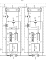
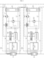
- FIGS. 2 and 3 are diagrams showing a path for the apparatus for battery module balancing according to an embodiment of the present disclosure to balance battery modules.
- the processor 230 may be configured to generate an induced electromotive force for the inductor 251 by means of the discharging current of the cell assembly flowing through the self-circulating path L1 by repeatedly turning on and off the first discharge MOSFET 252 and transfer the generated induced electromotive force to a neighboring battery module through the connection paths L2, L3.
- the processor 230 may allow a discharging current to flow on the self-circulating path L1 included in the second battery module 200. More specifically, when it is intended to discharge the second cell assembly 20 included in the second battery module 200 and charge the first cell assembly 10 included in the first battery module 100, the processor 230 may allow a discharging current to flow on the self-circulating path L1 included in the second battery module 200. For example, the processor 230 may turn on the first discharge MOSFET 252 included in the second battery module 200 so that the discharging current flows sequentially through the second cell assembly 20, the inductor 251 and the first discharge MOSFET 252.
- the processor 230 may turn off the first discharge MOSFET 252 included in the second battery module 200 to generate an induced electromotive force for the inductor 251.
- the inductor 251 may generate an induced electromotive force according to Faraday's law of Equation 1 below. That is, the inductor 251 may generate an induced electromotive force for maintaining the direction of the current of FIG. 2 .
- v t L dt t dt
- v(t) is an induced electromotive force
- L is inductance
- t is time
- i(t) is a current flowing through the inductor.
- the processor 230 may charge the first cell assembly 10 through the connection paths L2, L3 and the self-circulating path L1, which sequentially connect the inductor 251, the second discharge MOSFET 261, the connector 220 of the second battery module 200, the connector 120 of the first battery module 100 and the first cell assembly 10.
- the processor 230 may discharge the second cell assembly 20 and charge the first cell assembly 10 by repeatedly turning on and off the first discharge MOSFET 252.
- the apparatus for battery module balancing may effectively reduce the number of switches and resistors by using the induced electromotive force of the inductor and reduce the power loss consumed by the resistors, thereby effectively balancing the battery modules.
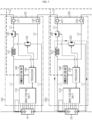
- FIGS. 4 and 5 are diagrams showing a path for the apparatus for battery module balancing according to another embodiment of the present disclosure to balance battery modules.
- the processor 230 may be configured to generate an induced electromotive force of the inductor 251 by means of the discharging current of the cell assembly flowing through the connection paths L2, L3 by repeatedly turning on and off the second discharge MOSFET 261 and transfer the generated induced electromotive force to a neighboring battery module through the self-circulating path L1.
- the processor 230 may allow a discharging current to flow through the self-circulating path L1 and the connection paths L2, L3 included in the first battery module 100 and the second battery module 200. More specifically, when it is intended to discharge the first cell assembly 10 included in the first battery module 100 and charge the second cell assembly 20 included in the second battery module 200, the processor 230 may allow a discharging current to flow through the self-circulating path L1 and the connection paths L2, L3 included in the first battery module 100.
- the processors 130, 230 allow a discharging current to sequentially flow through the first cell assembly 10, the connector 120 of the first battery module 100, the connector 220 of the second battery module 200, the second discharge MOSFET 261 and the inductor 251 by turning off the first discharge MOSFET 152 included in the first battery module 100 and turning on the second discharge MOSFET 261 included in the second battery module 200.
- the processor 230 may generate an induced electromotive force for the inductor 251 by turning off the second discharge MOSFET 261 included in the second battery module 200. For example, if the second discharge MOSFET 261 is changed from a turn-on state to a turn-off state, an induced electromotive force may be generated at the inductor 251 according to Faraday's law of Equation 1. That is, the inductor 251 may generate an induced electromotive force to maintain the direction of the current of FIG. 4 .
- the processor 230 may charge the second cell assembly 20 through the self-circulating path L1 that sequentially connects the inductor 251, the second cell assembly 20 and the first discharge MOSFET 252.
- the processor 230 may discharge the first cell assembly 10 and charge the second cell assembly 20 by repeatedly turning on and off the second discharge MOSFET 261.
- the apparatus for battery module balancing may easily configure lines of a balancing circuit and efficiently balance the plurality of battery modules through simple switch operations.
- the apparatus for battery module balancing according to the present disclosure may include a battery management system (BMS). That is, the BMS according to the present disclosure may be included in the apparatus for battery module balancing of the present disclosure as described above. In this configuration, at least a part of the components of the apparatus for battery module balancing according to the present disclosure may be implemented by supplementing or adding functionality of components included in the conventional BMS. For example, the processor and the memory device of the apparatus for battery module balancing according to the present disclosure may be implemented as components of the BMS.
- BMS battery management system
- the apparatus for battery module balancing according to the present disclosure may be provided to a battery pack. That is, the battery pack according to the present disclosure may include the apparatus for battery module balancing according to the present disclosure.
- the battery pack may include at least one secondary battery, the apparatus for battery module balancing, electrical components (such as a BMS, a relay and a fuse), a case, and so on.
- FIG. 6 is a schematic flowchart for illustrating a method for battery module balancing according to an embodiment of the present disclosure.
- each step may be performed by any component of the apparatus for battery module balancing according to the present disclosure as described above.
- the method for battery module balancing includes a monitoring step S100 and a balancing step S110.
- the monitoring step S 100 at least one of voltage, temperature and current of each cell assembly may be monitored.
- the state of each cell assembly monitored in the monitoring step may be received, and opening and closing operations of a first discharge MOSFET configured to open or close a self-circulating path, which is electrically connected to both ends of each cell assembly to form a closed circuit and has an inductor configured to allow a charging and discharging current to flow on the self-circulating path, and a second discharge MOSFET configured to open or close a connection path, which electrically connects both ends of the inductor to a plurality of connection terminals and electrically connects neighboring battery modules to each other through the plurality of connection terminals, may be controlled on the basis of the received state of each cell assembly so that the plurality of battery modules are balanced
- the charges of neighboring cell assemblies may be equalized through the self-circulating path and the connection path by repeatedly turning on and off the first discharge MOSFET or the second discharge MOSFET.
- an induced electromotive force may be generated at the inductor by means of the discharging current of the cell assembly flowing through the self-circulating path by repeatedly turning on and off the first discharge MOSFET, and the generated induced electromotive force may be transferred to a neighboring battery module through the connection path.
- an induced electromotive force may be generated at the inductor by means of the discharging current of the cell assembly flowing on the connection path by repeatedly turning on and off the second discharge MOSFET, and the induced electromotive force may be transferred to a neighboring battery module through the self-circulating path.
- the processor may be implemented as a set of program modules.
- the program modules may be stored in a memory device and executed by the processor.
- the types of various control logics of the processor there is no particular limitation on the types of various control logics of the processor, as long as one or more control logics are combined and the combined control logic is written in a computer-readable code system so that the computer-readable access is possible.
- the recording medium includes at least one selected from the group consisting of a ROM, a RAM, a register, a CD-ROM, a magnetic tape, a hard disk, a floppy disk and an optical data recording device.
- the code system may be stored and executed in a distributed manner on computers connected through a network.
- functional programs, code and segments for implementing the combined control logics may be easily inferred by programmers in the technical field to which the present disclosure belongs.
Landscapes
- Engineering & Computer Science (AREA)
- Power Engineering (AREA)
- Manufacturing & Machinery (AREA)
- Chemical & Material Sciences (AREA)
- Chemical Kinetics & Catalysis (AREA)
- Electrochemistry (AREA)
- General Chemical & Material Sciences (AREA)
- Microelectronics & Electronic Packaging (AREA)
- Secondary Cells (AREA)
- Charge And Discharge Circuits For Batteries Or The Like (AREA)
Description
- The present disclosure relates to an apparatus and method for battery module balancing, and more particularly, to an apparatus and method for battery module balancing capable of effectively equalizing charges of battery modules while balancing a plurality of battery modules included in a battery pack.
- In recent years, the demand for portable electronic products such as notebook computers, video cameras and portable phones has increased sharply, and the energy storage batteries, robots and satellites has been active developed. Accordingly, high-performance secondary batteries allowing repeated charging and discharging are being actively studied.
- Secondary batteries commercially available at present include nickel-cadmium batteries, nickel-hydrogen batteries, nickel-zinc batteries, lithium secondary batteries and the like. Among them, the lithium secondary batteries have almost no memory effect compared to nickel-based secondary batteries and thus are in the limelight due to advantageous such as free charging and discharging, low self-discharge rate and high energy density.
- Batteries are used in a wide variety of applications, and large capacities are often required for devices such as electric-driven vehicles or smart grid systems to which batteries are frequently utilized. In order to increase the capacity of the battery, the capacity of the secondary battery, namely the capacity of a battery cell itself, may be increased. However, in this case, the capacity increase effect is not large and there is a physical limitation on the size expansion of the secondary battery. Thus, generally, a battery pack in which a plurality of battery modules are connected in series and in parallel is widely used.
- The plurality of battery modules included in the battery pack have different capacity performances from each other due to the difference in intrinsic characteristics or manufacturing environments and versatility of system applications as the use time elapses, which causes a difference in terminal voltage or state of charge (SOC) of the corresponding modules due to charging and discharging.
- If a plurality of battery modules having different relative electrical characteristics are driven as one battery pack, a specific battery module having degraded performance may limit the charging or discharging capacity of the entire battery pack, age the battery pack and cause problems such as overvoltage.
- Evenly controlling the terminal voltages between battery modules is known as module balancing or inter-module charge equalization. However, in the conventional inter-module charge equalization technology, it is difficult to individually perform balancing between specific battery modules that require module balancing, among a plurality of battery modules. In particular, in order to implement a charge equalization circuit that individually selects a specific battery module, a circuit structure becomes complicated, and the number and volume of wiring bundles increase. Thus, due to these problems, it is not easy to manufacture a module equalization device, and the manufacturing process may take long time and suffer from a high defective rate.
-
- The present disclosure is designed to solve the problems of the related art, and therefore the present disclosure is directed to providing an apparatus and method for battery module balancing, which may effectively equalize charges between battery modules while balancing a plurality of battery modules included in a battery pack.
- These and other objects and advantages of the present disclosure may be understood from the following detailed description and will become more fully apparent from the exemplary embodiments of the present disclosure. Also, it will be easily understood that the objects and advantages of the present disclosure may be realized by the means shown in the appended claims and combinations thereof.
- In order to accomplish the above object, an apparatus for battery module balancing according to an embodiment, as defined by independent claim 1, balances a plurality of battery modules that respectively include cell assemblies having at least one secondary battery and electrically connected in series, the apparatus for battery module balancing comprising: a monitoring unit provided to each battery module and configured to monitor at least one of voltage, temperature and current of each cell assembly; a self-circulating path provided to each battery module and electrically connected to both ends of each cell assembly to form a closed circuit, the self-circulating path having an inductor configured to allow a charging and discharging current to flow on the self-circulating path and a first discharge MOSFET configured to open or close the self-circulating path: a connector provided to each battery module and configured to have a plurality of connection terminals; a connection path provided to each battery module to electrically connect both ends of the inductor to the plurality of connection terminals and electrically connect neighboring battery modules to each other through the plurality of connection terminals, the connection path having a second discharge MOSFET provided on the connection path to open or close the connection path; and a processor configured to receive a state of each cell assembly from the monitoring unit and control opening and closing operations of the first discharge MOSFET and the second discharge MOSFET on the basis of the received state of each cell assembly so that the plurality of battery modules are balanced.
- In addition, the processor may be configured to repeatedly turn on and off the first discharge MOSFET or the second discharge MOSFET so that charges of neighboring cell assemblies are equalized through the self-circulating path and the connection path.
- In addition, the processor may be configured to repeatedly turn on and off the first discharge MOSFET to generate an induced electromotive force with respect to the inductor by means of a discharging current of the cell assembly flowing through the self-circulating path and transmit the generated induced electromotive force to a neighboring battery module through the connection path.
- In addition, the processor may be configured to repeatedly turn on and off the second discharge MOSFET to generate an induced electromotive force of the inductor by means of a discharging current of the cell assembly flowing through the connection path and transmit the generated induced electromotive force to a neighboring battery module through the self-circulating path.
- The connection path includes a first internal connection path and a second internal connection path, the plurality of connection terminals may include a first connection terminal and a second connection terminal, the first internal connection path may be configured to electrically connect a node between a positive electrode terminal of each cell assembly and one end of the inductor directly to the first connection terminal, and the second internal connection path may be configured to electrically connect a node between the other end of the inductor and the first discharge MOSFET directly to the second connection terminal.
- In addition, the second discharge MOSFET may be configured to be provided on the second internal connection path.
- In addition, the connection path may further include an external connection path configured to electrically connect the first connection terminal and the second connection terminal of each battery module directly to the second connection terminal and the first connection terminal of a neighboring battery module, respectively.
- In addition, in order to accomplish the above object, a battery management system (BMS) according to an embodiment of the present disclosure comprises the apparatus for battery module balancing according to the present disclosure.
- In addition, in order to accomplish the above object, a battery pack according to an embodiment of the present disclosure comprises the apparatus for battery module balancing according to the present disclosure.
- In addition, in order to accomplish the above object, a method for battery module balancing according to an embodiment of the present disclosure balances a plurality of battery modules that respectively include cell assemblies having at least one secondary battery and electrically connected in series, the method for battery module balancing comprising: monitoring at least one of voltage, temperature and current of each cell assembly; and receiving a state of each cell assembly, which is monitored in the monitoring step, and controlling opening and closing operations of a first discharge MOSFET configured to open or close a self-circulating path, which is electrically connected to both ends of each cell assembly to form a closed circuit and has an inductor configured to allow a charging and discharging current to flow on the self-circulating path, and a second discharge MOSFET configured to open or close a connection path, which electrically connects both ends of the inductor to a plurality of connection terminals and electrically connects neighboring battery modules to each other through the plurality of connection terminals, on the basis of the received state of each cell assembly so that the plurality of battery modules are balanced.
- According to the present disclosure, it is possible to allow easy manufacture of the battery pack and easily reduction of its size since connectors may be simplified and the volume of wire harness may be reduced, when individually selecting battery modules to which charging and discharging are required for charge equalization of the battery modules.
- In addition, in the configuration of individually selecting battery modules, there is an advantage that the structure of the wiring connected to the battery modules is simplified and the charge equalization speed between the battery modules is increased.
- In addition, the battery module equalization device according to the present disclosure has an advantage of simplifying the charge equalization circuit by easily transferring energy between the battery modules without an external power connection.
- In addition, according to an aspect of the present disclosure, it is possible to reduce the number of switches and resistors by using the induced electromotive force of the inductor and to reduce the power loss consumed by the resistors, thereby effectively balancing the battery modules.
- The present disclosure may have various effects other than the above, and other effects of the present disclosure may be understood from the following description and more clearly figured out by the embodiments of the present disclosure.
- The accompanying drawings illustrate a preferred embodiment of the present disclosure and together with the foregoing disclosure, serve to provide further understanding of the technical features of the present disclosure, and thus, the present disclosure is not construed as being limited to the drawing.
-
FIG. 1 is a diagram schematically showing some components of an apparatus for battery module balancing according to an embodiment of the present disclosure. -
FIGS. 2 and3 are diagrams showing a path for the apparatus for battery module balancing according to an embodiment of the present disclosure to balance battery modules. -
FIGS. 4 and5 are diagrams showing a path for the apparatus for battery module balancing according to another embodiment of the present disclosure to balance battery modules. -
FIG. 6 is a flowchart schematically showing a method for battery module balancing according to an embodiment of the present disclosure. - Hereinafter, preferred embodiments of the present disclosure will be described in detail with reference to the accompanying drawings. Prior to the description, it should be understood that the terms used in the specification and the appended claims should not be construed as limited to general and dictionary meanings, but interpreted based on the meanings and concepts corresponding to technical aspects of the present disclosure on the basis of the principle that the inventor is allowed to define terms appropriately for the best explanation.
- Therefore, the description proposed herein is just a preferable example for the purpose of illustrations only, not intended to limit the scope of the disclosure, so it should be understood that other equivalents and modifications could be made thereto without departing from the scope of the disclosure.
- In addition, in the present disclosure, if it is determined that a detailed description of a related known structure or function may obscure the subject matter of the present disclosure, the detailed description will be omitted.
- Throughout the specification, when a portion is referred to as "comprising" or "including" any element, it means that the portion may include other elements further, without excluding other elements, unless specifically stated otherwise. Furthermore, the term "processor" described in the specification refers to a unit that processes at least one function or operation, and may be implemented by hardware, software, or a combination of hardware and software.
- In addition, throughout the specification, when a portion is referred to as being "connected" to another portion, it is not limited to the case that they are "directly connected", but it also includes the case where they are "indirectly connected" with another element being interposed between them.
- In this specification, the secondary battery refers to a one independent cell that includes a negative electrode terminal and a positive electrode terminal and is physically separable. For example, one pouch-type lithium polymer cell may be regarded as the secondary battery.
- An apparatus for battery module balancing according to an embodiment of the present disclosure may be an apparatus for balancing a plurality of
battery modules battery modules cell assemblies -
FIG. 1 is a diagram schematically showing some components of an apparatus for battery module balancing according to an embodiment of the present disclosure. - Referring to
FIG. 1 , the apparatus for battery module balancing according to an embodiment of the present disclosure includesmonitoring units connectors processors - The
monitoring units battery modules FIG. 1 , themonitoring units cell assemblies battery modules monitoring units cell assemblies monitoring units - In addition, the
monitoring units cell assembly monitoring units cell assembly units FIG. 1 , the monitoringunits cell assemblies units processors units processors processors units cell assemblies processors processors cell assemblies units units - In addition, the monitoring
units cell assemblies FIG. 1 , the monitoringunits cell assemblies units processors processors units cell assemblies processors processors units - In addition, the monitoring
units cell assemblies FIG. 1 , the monitoringunits cell assemblies cell assemblies units processors units cell assemblies processors processors units units - The self-circulating path L1 may be provided to each
battery module cell assembly FIG. 1 , the self-circulating path L1 may be provided to eachbattery module cell assemblies cell assemblies cell assemblies - In addition, the self-circulating path L1 may include
inductors first discharge MOSFETs - The
inductors FIG. 1 , theinductors inductors cell assemblies inductors inductors - The
first discharge MOSFETs FIG. 1 , thefirst discharge MOSFETs first discharge MOSFETs inductors cell assemblies first discharge MOSFETs processors processors - The
connectors battery modules FIG. 1 , theconnectors battery modules connectors FIG. 1 , theconnectors connectors battery modules - The connection paths L2, L3 may be provided to the
battery modules inductors connection terminals battery modules connection terminals FIG. 1 , the connection paths L2, L3 may be provided to thebattery modules inductors connection terminals connection terminals battery modules battery modules - In addition, the connection paths L2, L3 may include
second discharge MOSFETs second discharge MOSFETs FIG. 1 , thesecond discharge MOSFETs second discharge MOSFETs inductors connection terminals second discharge MOSFETs processors processors - Preferably, the
first discharge MOSFETs second discharge MOSFETs - In addition, the
first discharge MOSFETs second discharge MOSFETs - For example, as shown in
FIG. 1 , in thefirst discharge MOSFETs inductors cell assemblies first discharge MOSFETs first discharge MOSFETs cell assemblies inductors - For example, as shown in
FIG. 1 , in thesecond discharge MOSFETs connection terminals inductors second discharge MOSFETs second discharge MOSFETs inductors connection terminals - In addition, the
processors first discharge MOSFETs second discharge MOSFETs FIG. 1 , theprocessors first discharge MOSFETs second discharge MOSFETs processors first discharge MOSFETs second discharge MOSFETs first discharge MOSFETs second discharge MOSFETs - Preferably, the connection paths L2, L3 according to an embodiment of the present disclosure may include a first internal connection path L2 and a second internal connection path L2. In addition, the plurality of
connection terminals first connection terminals second connection terminals - As shown in
FIG. 1 , the first internal connection path L2 may be configured to electrically connect a node between the positive electrode terminal of eachcell assembly inductors first connection terminals - As shown in
FIG. 1 , the second internal connection path L2 may be configured to electrically connect a node between the other end of theinductors first discharge MOSFETs second connection terminals - Preferably, the
second discharge MOSFETs FIG. 1 , thesecond discharge MOSFETs inductors first discharge MOSFETs second connection terminal - Preferably, the connection paths L2, L3 according to an embodiment of the present disclosure may further include an external connection path L3.
- The external connection path L3 may be configured to be electrically connect the
first connection terminals second connection terminal battery module second connection terminal first connection terminals battery module FIG. 1 , the external connection path L3 may electrically connect thesecond connection terminal 221 of thesecond battery module 200 directly to thefirst connection terminal 122 of thefirst battery module 100. In addition, preferably, the external connection path L3 according to an embodiment of the present disclosure may connect thebattery modules - The
processors monitoring units cell assemblies units cell assemblies processors units processors - In addition, the
processors cell assemblies units cell assemblies cell assemblies cell assemblies cell assemblies cell assemblies - In addition, the
processors cell assemblies units processors - In an embodiment of the present disclosure, the
processors processors - In another embodiment of the present disclosure, the
processors - More preferably, the
processors units - In addition, the
processors battery modules first discharge MOSFETs second discharge MOSFETs cell assemblies - Preferably, the
processors cell assemblies first discharge MOSFETs second discharge MOSFETs - Preferably, as shown in
FIG. 1 , the apparatus for battery module balancing according to an embodiment of the present disclosure may further includecommunication units - The
communication units processors processors battery modules communication units processors battery modules battery modules - Preferably, the apparatus for battery module balancing according to an embodiment of the present disclosure may further include a memory device.
- The memory device may be electrically connected to the
processors first discharge MOSFETs second discharge MOSFETs - Meanwhile, the
processors processors - Meanwhile, the memory device is not particularly limited as long as it is a storage medium capable of recording and erasing information. For example, the memory device may be a RAM, a ROM, a register, a hard disk, an optical recording medium, or a magnetic recording medium. The memory device may also be electrically connected to the
processors processors processors -
FIGS. 2 and3 are diagrams showing a path for the apparatus for battery module balancing according to an embodiment of the present disclosure to balance battery modules. - Referring to
FIGS. 2 and3 , theprocessor 230 according to an embodiment of the present disclosure may be configured to generate an induced electromotive force for theinductor 251 by means of the discharging current of the cell assembly flowing through the self-circulating path L1 by repeatedly turning on and off thefirst discharge MOSFET 252 and transfer the generated induced electromotive force to a neighboring battery module through the connection paths L2, L3. - For example, as shown in
FIG. 2 , theprocessor 230 may allow a discharging current to flow on the self-circulating path L1 included in thesecond battery module 200. More specifically, when it is intended to discharge thesecond cell assembly 20 included in thesecond battery module 200 and charge thefirst cell assembly 10 included in thefirst battery module 100, theprocessor 230 may allow a discharging current to flow on the self-circulating path L1 included in thesecond battery module 200. For example, theprocessor 230 may turn on thefirst discharge MOSFET 252 included in thesecond battery module 200 so that the discharging current flows sequentially through thesecond cell assembly 20, theinductor 251 and thefirst discharge MOSFET 252. - In addition, as shown in
FIG. 3 , theprocessor 230 may turn off thefirst discharge MOSFET 252 included in thesecond battery module 200 to generate an induced electromotive force for theinductor 251. For example, if thefirst discharge MOSFET 252 is changed from a turn-on state to a turn-off state, theinductor 251 may generate an induced electromotive force according to Faraday's law of Equation 1 below. That is, theinductor 251 may generate an induced electromotive force for maintaining the direction of the current ofFIG. 2 .
- Here, v(t) is an induced electromotive force, L is inductance, t is time, and i(t) is a current flowing through the inductor.
- In addition, as shown in
FIG. 3 , when an induced electromotive force is generated at theinductor 251, theprocessor 230 may charge thefirst cell assembly 10 through the connection paths L2, L3 and the self-circulating path L1, which sequentially connect theinductor 251, thesecond discharge MOSFET 261, theconnector 220 of thesecond battery module 200, theconnector 120 of thefirst battery module 100 and thefirst cell assembly 10. - Through this configuration, the
processor 230 may discharge thesecond cell assembly 20 and charge thefirst cell assembly 10 by repeatedly turning on and off thefirst discharge MOSFET 252. - Through this configuration, the apparatus for battery module balancing according to an embodiment of the present disclosure may effectively reduce the number of switches and resistors by using the induced electromotive force of the inductor and reduce the power loss consumed by the resistors, thereby effectively balancing the battery modules.
-
FIGS. 4 and5 are diagrams showing a path for the apparatus for battery module balancing according to another embodiment of the present disclosure to balance battery modules. - Referring to
FIGS. 4 and5 , theprocessor 230 according to an embodiment of the present disclosure may be configured to generate an induced electromotive force of theinductor 251 by means of the discharging current of the cell assembly flowing through the connection paths L2, L3 by repeatedly turning on and off thesecond discharge MOSFET 261 and transfer the generated induced electromotive force to a neighboring battery module through the self-circulating path L1. - For example, as shown in
FIG. 4 , theprocessor 230 may allow a discharging current to flow through the self-circulating path L1 and the connection paths L2, L3 included in thefirst battery module 100 and thesecond battery module 200. More specifically, when it is intended to discharge thefirst cell assembly 10 included in thefirst battery module 100 and charge thesecond cell assembly 20 included in thesecond battery module 200, theprocessor 230 may allow a discharging current to flow through the self-circulating path L1 and the connection paths L2, L3 included in thefirst battery module 100. For example, theprocessors first cell assembly 10, theconnector 120 of thefirst battery module 100, theconnector 220 of thesecond battery module 200, thesecond discharge MOSFET 261 and theinductor 251 by turning off thefirst discharge MOSFET 152 included in thefirst battery module 100 and turning on thesecond discharge MOSFET 261 included in thesecond battery module 200. - In addition, as shown in
FIG. 5 , theprocessor 230 may generate an induced electromotive force for theinductor 251 by turning off thesecond discharge MOSFET 261 included in thesecond battery module 200. For example, if thesecond discharge MOSFET 261 is changed from a turn-on state to a turn-off state, an induced electromotive force may be generated at theinductor 251 according to Faraday's law of Equation 1. That is, theinductor 251 may generate an induced electromotive force to maintain the direction of the current ofFIG. 4 . - In addition, as shown in
FIG. 5 , if the induced electromotive force is generated at theinductor 251, theprocessor 230 may charge thesecond cell assembly 20 through the self-circulating path L1 that sequentially connects theinductor 251, thesecond cell assembly 20 and thefirst discharge MOSFET 252. - Through this configuration, the
processor 230 may discharge thefirst cell assembly 10 and charge thesecond cell assembly 20 by repeatedly turning on and off thesecond discharge MOSFET 261. - Through this configuration, the apparatus for battery module balancing according to an embodiment of the present disclosure may easily configure lines of a balancing circuit and efficiently balance the plurality of battery modules through simple switch operations.
- The apparatus for battery module balancing according to the present disclosure may include a battery management system (BMS). That is, the BMS according to the present disclosure may be included in the apparatus for battery module balancing of the present disclosure as described above. In this configuration, at least a part of the components of the apparatus for battery module balancing according to the present disclosure may be implemented by supplementing or adding functionality of components included in the conventional BMS. For example, the processor and the memory device of the apparatus for battery module balancing according to the present disclosure may be implemented as components of the BMS.
- In addition, the apparatus for battery module balancing according to the present disclosure may be provided to a battery pack. That is, the battery pack according to the present disclosure may include the apparatus for battery module balancing according to the present disclosure. Here, the battery pack may include at least one secondary battery, the apparatus for battery module balancing, electrical components (such as a BMS, a relay and a fuse), a case, and so on.
-
FIG. 6 is a schematic flowchart for illustrating a method for battery module balancing according to an embodiment of the present disclosure. InFIG. 6 , each step may be performed by any component of the apparatus for battery module balancing according to the present disclosure as described above. - As shown in
FIG. 6 , the method for battery module balancing according to the present disclosure includes a monitoring step S100 and a balancing step S110. - First, in the
monitoring step S 100, at least one of voltage, temperature and current of each cell assembly may be monitored. Subsequently, in the balancing step S110, the state of each cell assembly monitored in the monitoring step may be received, and opening and closing operations of a first discharge MOSFET configured to open or close a self-circulating path, which is electrically connected to both ends of each cell assembly to form a closed circuit and has an inductor configured to allow a charging and discharging current to flow on the self-circulating path, and a second discharge MOSFET configured to open or close a connection path, which electrically connects both ends of the inductor to a plurality of connection terminals and electrically connects neighboring battery modules to each other through the plurality of connection terminals, may be controlled on the basis of the received state of each cell assembly so that the plurality of battery modules are balanced - Preferably, in the
balancing step S 110 according to an embodiment of the present disclosure, the charges of neighboring cell assemblies may be equalized through the self-circulating path and the connection path by repeatedly turning on and off the first discharge MOSFET or the second discharge MOSFET. - Preferably, in the balancing step S110 according to an embodiment of the present disclosure, an induced electromotive force may be generated at the inductor by means of the discharging current of the cell assembly flowing through the self-circulating path by repeatedly turning on and off the first discharge MOSFET, and the generated induced electromotive force may be transferred to a neighboring battery module through the connection path.
- Preferably, in the balancing step S110 according to an embodiment of the present disclosure, an induced electromotive force may be generated at the inductor by means of the discharging current of the cell assembly flowing on the connection path by repeatedly turning on and off the second discharge MOSFET, and the induced electromotive force may be transferred to a neighboring battery module through the self-circulating path.
- Also, when the control logic is implemented in software, the processor may be implemented as a set of program modules. At this time, the program modules may be stored in a memory device and executed by the processor.
- In addition, there is no particular limitation on the types of various control logics of the processor, as long as one or more control logics are combined and the combined control logic is written in a computer-readable code system so that the computer-readable access is possible. As one example, the recording medium includes at least one selected from the group consisting of a ROM, a RAM, a register, a CD-ROM, a magnetic tape, a hard disk, a floppy disk and an optical data recording device. In addition, the code system may be stored and executed in a distributed manner on computers connected through a network. Moreover, functional programs, code and segments for implementing the combined control logics may be easily inferred by programmers in the technical field to which the present disclosure belongs.
- The present disclosure has been described in detail. However, it should be understood that the detailed description and specific examples, while indicating preferred embodiments of the disclosure, are given by way of illustration only, since various changes and modifications within the scope of the disclosure will become apparent to those skilled in the art from this detailed description. However, the scope of the invention is solely defined by the appended claims.
-
- 10: first cell assembly
- 20: second cell assembly
- 100: first battery module
- 110: monitoring unit
- 120: connector
- 121: second connection terminal
- 122: first connection terminal
- 130: processor
- 140: communication unit
- 151: inductor
- 152: first discharge MOSFET
- 161: second discharge MOSFET
- 200: second battery module
- 210: monitoring unit
- 220: connector
- 221: second connection terminal
- 222: first connection terminal
- 230: processor
- 240: communication unit
- 251: inductor
- 252: first discharge MOSFET
- 261: second discharge MOSFET
- L1: self-circulating path
- L2: internal connection path
- L3: external connection path
Claims (9)
- An apparatus for battery module balancing, configured to balance a plurality of battery modules (100, 200) that respectively include cell assemblies (10, 20) having at least one secondary battery and electrically connected in series, the apparatus for battery module balancing comprising:a monitoring unit (110; 210) provided to each battery module and configured to monitor at least one of voltage, temperature and current of each cell assembly;a self-circulating path (L1) provided to each battery module and electrically connected to both ends of each cell assembly to form a closed circuit, the self-circulating path having an inductor (151; 251) configured to allow a charging and discharging current to flow on the self-circulating path and a first discharge MOSFET (152; 252) configured to open or close the self-circulating path;a connector (120; 220) provided to each battery module and configured to have a plurality of connection terminals (121, 122; 221, 222);a connection path (L2, L3) provided to each battery module to electrically connect both ends of the inductor to the plurality of connection terminals and electrically connect neighboring battery modules to each other through the plurality of connection terminals, the connection path having a second discharge MOSFET (161; 261) provided on the connection path to open or close the connection path; anda processor (130, 230) configured to receive a state of each cell assembly from the monitoring unit and control opening and closing operations of the first discharge MOSFET and the second discharge MOSFET on the basis of the received state of each cell assembly so that the plurality of battery modules are balanced;
characterised in thatthe connection path includes a first internal connection path (L2) and a second internal connection path (L2), and the plurality of connection terminals include a first connection terminal (122) and a second connection terminal (121),wherein the first internal connection path is configured to electrically connect a node between a positive electrode terminal of each cell assembly and one end of the inductor directly to the first connection terminal, andwherein the second internal connection path is configured to electrically connect a node between the other end of the inductor and the first discharge MOSFET directly to the second connection terminal. - The apparatus for battery module balancing according to claim 1,
wherein the processor is configured to repeatedly turn on and off the first discharge MOSFET or the second discharge MOSFET so that charges of neighboring cell assemblies are equalized through the self-circulating path and the connection path. - The apparatus for battery module balancing according to claim 1,
wherein the processor is configured to repeatedly turn on and off the first discharge MOSFET to generate an induced electromotive force with respect to the inductor by means of a discharging current of the cell assembly flowing through the self-circulating path and transmit the generated induced electromotive force to a neighboring battery module through the connection path. - The apparatus for battery module balancing according to claim 1,
wherein the processor is configured to repeatedly turn on and off the second discharge MOSFET to generate an induced electromotive force of the inductor by means of a discharging current of the cell assembly flowing through the connection path and transmit the generated induced electromotive force to a neighboring battery module through the self-circulating path. - The apparatus for battery module balancing according to claim 1,
wherein the second discharge MOSFET is configured to be provided on the second internal connection path. - The apparatus for battery module balancing according to claim 1,
wherein the connection path further includes an external connection path (L3) configured to electrically connect the first connection terminal and the second connection terminal of each battery module directly to the second connection terminal and the first connection terminal of a neighboring battery module, respectively. - A battery management system, BMS, comprising the apparatus for battery module balancing according to any one of claims 1 to 6.
- A battery pack, comprising the apparatus for battery module balancing according to any one of claims 1 to 6.
- A method for battery module balancing by means of the apparatus of claim 1, which balances a plurality of battery modules that respectively include cell assemblies having at least one secondary battery and electrically connected in series, the method comprising:monitoring at least one of voltage, temperature and current of each cell assembly; andreceiving a state of each cell assembly, which is monitored in the monitoring step, and controlling opening and closing operations of a first discharge MOSFET configured to open or close a self-circulating path, which is electrically connected to both ends of each cell assembly to form a closed circuit and has an inductor configured to allow a charging and discharging current to flow on the self-circulating path, and a second discharge MOSFET configured to open or close a connection path, which electrically connects both ends of the inductor to a plurality of connection terminals and electrically connects neighboring battery modules to each other through the plurality of connection terminals, on the basis of the received state of each cell assembly so that the plurality of battery modules are balanced.
Applications Claiming Priority (2)
| Application Number | Priority Date | Filing Date | Title |
|---|---|---|---|
| KR1020180123412A KR102374744B1 (en) | 2018-10-16 | 2018-10-16 | Apparatus and method for balancing of battery module |
| PCT/KR2019/013525 WO2020080802A1 (en) | 2018-10-16 | 2019-10-15 | Apparatus and method for battery module balancing |
Publications (3)
| Publication Number | Publication Date |
|---|---|
| EP3790150A1 EP3790150A1 (en) | 2021-03-10 |
| EP3790150A4 EP3790150A4 (en) | 2021-08-11 |
| EP3790150B1 true EP3790150B1 (en) | 2024-09-18 |
Family
ID=70284017
Family Applications (1)
| Application Number | Title | Priority Date | Filing Date |
|---|---|---|---|
| EP19873876.7A Active EP3790150B1 (en) | 2018-10-16 | 2019-10-15 | Apparatus and method for battery module balancing |
Country Status (8)
| Country | Link |
|---|---|
| US (1) | US11258274B2 (en) |
| EP (1) | EP3790150B1 (en) |
| JP (1) | JP7049567B2 (en) |
| KR (1) | KR102374744B1 (en) |
| CN (1) | CN111919356B (en) |
| ES (1) | ES2989115T3 (en) |
| HU (1) | HUE068460T2 (en) |
| WO (1) | WO2020080802A1 (en) |
Families Citing this family (5)
| Publication number | Priority date | Publication date | Assignee | Title |
|---|---|---|---|---|
| KR102150147B1 (en) * | 2017-05-24 | 2020-09-01 | 주식회사 엘지화학 | Apparatus and method for balancing battery module |
| KR102202613B1 (en) * | 2017-09-27 | 2021-01-12 | 주식회사 엘지화학 | Apparatus for equalizing battery module, battery pack including the same, and vehicle |
| JP7077204B2 (en) * | 2018-10-31 | 2022-05-30 | 株式会社豊田中央研究所 | Power supply |
| KR102902823B1 (en) * | 2021-12-01 | 2025-12-19 | 주식회사 엘지에너지솔루션 | Cell voltage estimation method and battery system providing the same |
| KR102499839B1 (en) * | 2022-06-29 | 2023-02-14 | (주)그린파워 | Series connection structure of pouch-type battery cells apply to series battery charging/discharging device |
Family Cites Families (24)
| Publication number | Priority date | Publication date | Assignee | Title |
|---|---|---|---|---|
| US5742150A (en) * | 1996-09-16 | 1998-04-21 | Khuwatsamrit; Thakoengdet | Power supply and method of protecting batteries therein |
| FR2825842B1 (en) | 2001-06-07 | 2003-10-03 | Cit Alcatel | BALANCING METHOD FOR ELECTRIC BATTERY SUBJECT TO A DISCONTINUOUS RECHARGE REGIMEN AND BATTERY MANAGEMENT SYSTEM FOR CARRYING OUT SAID METHOD |
| KR101107999B1 (en) * | 2007-10-16 | 2012-01-25 | 한국과학기술원 | Battery Operating System Combines Voltage Sensor and Charge Uniformity |
| KR101156977B1 (en) * | 2007-12-31 | 2012-06-20 | 에스케이이노베이션 주식회사 | Method for Balancing of High Voltage Battery Pack |
| US8466657B2 (en) * | 2008-10-31 | 2013-06-18 | Bren-Tronics Batteries International, L.L.C. | Autonomous balancing of series connected charge storage devices |
| KR101122598B1 (en) * | 2009-02-15 | 2012-03-19 | 김래영 | Apparatus for uniform charging battery |
| US8884580B2 (en) * | 2010-09-28 | 2014-11-11 | Atmel Automotive Gmbh | Charge equalization between series-connected battery cells |
| JP5569418B2 (en) | 2011-02-01 | 2014-08-13 | 株式会社デンソー | Battery monitoring device |
| TW201246751A (en) * | 2011-05-12 | 2012-11-16 | Lite On Clean Energy Technology Corp | A battery system and a battery equalizer |
| US8692516B2 (en) | 2011-09-23 | 2014-04-08 | Linear Technology Corporation | Stackable bi-directional multicell battery balancer |
| JP2013116008A (en) | 2011-11-30 | 2013-06-10 | Toyota Industries Corp | Cell balance device |
| US20130266826A1 (en) * | 2012-03-13 | 2013-10-10 | Maxwell Technologies, Inc. | Ultracapacitor/battery combination and bus bar system |
| JP2013247690A (en) * | 2012-05-23 | 2013-12-09 | Toyota Industries Corp | Voltage equalization device |
| TWI501507B (en) | 2012-07-13 | 2015-09-21 | 蔡富生 | Method and apparatus for battery unit control by means of virtual battery mechanism |
| JP6134520B2 (en) * | 2013-01-25 | 2017-05-24 | Fdk株式会社 | Balance correction device and power storage device |
| JP6133110B2 (en) | 2013-04-09 | 2017-05-24 | Evtd株式会社 | Balance correction device and power storage system |
| KR20140140355A (en) * | 2013-05-29 | 2014-12-09 | 삼성에스디아이 주식회사 | Battery management system and driving method thereof |
| KR102564853B1 (en) | 2015-04-21 | 2023-08-09 | 삼성전자주식회사 | Battery control apparatus, battery module, battery pack, and battery control method |
| US10293693B2 (en) | 2015-04-21 | 2019-05-21 | Samsung Electronics Co., Ltd. | Battery control method and apparatus, battery module, and battery pack |
| KR101780396B1 (en) | 2015-06-29 | 2017-09-20 | 주식회사 코캄일렉트로닉스 | Apparatus and method for protecting battery |
| US9923247B2 (en) | 2015-09-11 | 2018-03-20 | Powin Energy Corporation | Battery pack with integrated battery management system |
| CN105871006A (en) * | 2016-04-14 | 2016-08-17 | 宁波飞驰达电子科技发展有限公司 | Detection and active balance charging system for lithium ion battery pack |
| KR20180123412A (en) | 2017-05-08 | 2018-11-16 | 이시창 | Contents service system and method |
| CN107359662B (en) * | 2017-08-01 | 2023-06-20 | 华南理工大学 | A battery management system with parallel equalization function and equalization method |
-
2018
- 2018-10-16 KR KR1020180123412A patent/KR102374744B1/en active Active
-
2019
- 2019-10-15 WO PCT/KR2019/013525 patent/WO2020080802A1/en not_active Ceased
- 2019-10-15 HU HUE19873876A patent/HUE068460T2/en unknown
- 2019-10-15 EP EP19873876.7A patent/EP3790150B1/en active Active
- 2019-10-15 ES ES19873876T patent/ES2989115T3/en active Active
- 2019-10-15 US US17/042,449 patent/US11258274B2/en active Active
- 2019-10-15 JP JP2020547372A patent/JP7049567B2/en active Active
- 2019-10-15 CN CN201980023420.2A patent/CN111919356B/en active Active
Also Published As
| Publication number | Publication date |
|---|---|
| ES2989115T3 (en) | 2024-11-25 |
| US11258274B2 (en) | 2022-02-22 |
| CN111919356A (en) | 2020-11-10 |
| KR20200042802A (en) | 2020-04-24 |
| EP3790150A1 (en) | 2021-03-10 |
| CN111919356B (en) | 2024-02-20 |
| WO2020080802A1 (en) | 2020-04-23 |
| HUE068460T2 (en) | 2024-12-28 |
| JP2021516529A (en) | 2021-07-01 |
| KR102374744B1 (en) | 2022-03-14 |
| JP7049567B2 (en) | 2022-04-07 |
| US20210083485A1 (en) | 2021-03-18 |
| EP3790150A4 (en) | 2021-08-11 |
Similar Documents
| Publication | Publication Date | Title |
|---|---|---|
| EP3790150B1 (en) | Apparatus and method for battery module balancing | |
| EP4202464B1 (en) | Battery management system, battery pack, electric vehicle and battery management method | |
| EP3734307B1 (en) | Current measuring apparatus, current measuring method and battery pack including the current measuring apparatus | |
| US20210041502A1 (en) | Switch Diagnosing Apparatus and Method | |
| Garche et al. | Battery management systems (BMS) for increasing battery life time | |
| EP3672021B1 (en) | Apparatus for preventing over-discharge | |
| KR102364237B1 (en) | Apparatus and method for pre-charging | |
| US10545185B2 (en) | Apparatus and method for diagnosing current sensor | |
| EP3754350B1 (en) | Switch diagnosing apparatus and method | |
| EP3667343B1 (en) | Apparatus and method for measuring voltage | |
| CN211018294U (en) | Charge Control Units, Battery Management Systems and Battery Packs | |
| EP3748388B1 (en) | Apparatus and method for diagnosing current sensor | |
| KR20200000182A (en) | Apparatus and method for operating battery | |
| KR20200062875A (en) | Apparatus for estimating depth of self-discharging | |
| KR20200038818A (en) | Apparatus and method for diagnosing current sensor | |
| KR102452596B1 (en) | Apparatus and method for diagnosing MOSFET | |
| KR20200004650A (en) | Apparatus and method for pre-charging dual battery | |
| KR20200054031A (en) | Apparatus and method for detecting disconnection of wire in battery |
Legal Events
| Date | Code | Title | Description |
|---|---|---|---|
| STAA | Information on the status of an ep patent application or granted ep patent |
Free format text: STATUS: THE INTERNATIONAL PUBLICATION HAS BEEN MADE |
|
| PUAI | Public reference made under article 153(3) epc to a published international application that has entered the european phase |
Free format text: ORIGINAL CODE: 0009012 |
|
| STAA | Information on the status of an ep patent application or granted ep patent |
Free format text: STATUS: REQUEST FOR EXAMINATION WAS MADE |
|
| 17P | Request for examination filed |
Effective date: 20201202 |
|
| AK | Designated contracting states |
Kind code of ref document: A1 Designated state(s): AL AT BE BG CH CY CZ DE DK EE ES FI FR GB GR HR HU IE IS IT LI LT LU LV MC MK MT NL NO PL PT RO RS SE SI SK SM TR |
|
| AX | Request for extension of the european patent |
Extension state: BA ME |
|
| A4 | Supplementary search report drawn up and despatched |
Effective date: 20210709 |
|
| RIC1 | Information provided on ipc code assigned before grant |
Ipc: H02J 7/00 20060101AFI20210705BHEP |
|
| DAV | Request for validation of the european patent (deleted) | ||
| DAX | Request for extension of the european patent (deleted) | ||
| RAP1 | Party data changed (applicant data changed or rights of an application transferred) |
Owner name: LG ENERGY SOLUTION LTD. |
|
| RAP3 | Party data changed (applicant data changed or rights of an application transferred) |
Owner name: LG ENERGY SOLUTION, LTD. |
|
| GRAP | Despatch of communication of intention to grant a patent |
Free format text: ORIGINAL CODE: EPIDOSNIGR1 |
|
| STAA | Information on the status of an ep patent application or granted ep patent |
Free format text: STATUS: GRANT OF PATENT IS INTENDED |
|
| INTG | Intention to grant announced |
Effective date: 20240417 |
|
| P01 | Opt-out of the competence of the unified patent court (upc) registered |
Effective date: 20240430 |
|
| GRAS | Grant fee paid |
Free format text: ORIGINAL CODE: EPIDOSNIGR3 |
|
| GRAA | (expected) grant |
Free format text: ORIGINAL CODE: 0009210 |
|
| STAA | Information on the status of an ep patent application or granted ep patent |
Free format text: STATUS: THE PATENT HAS BEEN GRANTED |
|
| AK | Designated contracting states |
Kind code of ref document: B1 Designated state(s): AL AT BE BG CH CY CZ DE DK EE ES FI FR GB GR HR HU IE IS IT LI LT LU LV MC MK MT NL NO PL PT RO RS SE SI SK SM TR |
|
| REG | Reference to a national code |
Ref country code: GB Ref legal event code: FG4D |
|
| REG | Reference to a national code |
Ref country code: CH Ref legal event code: EP |
|
| REG | Reference to a national code |
Ref country code: DE Ref legal event code: R096 Ref document number: 602019059246 Country of ref document: DE |
|
| REG | Reference to a national code |
Ref country code: IE Ref legal event code: FG4D |
|
| REG | Reference to a national code |
Ref country code: ES Ref legal event code: FG2A Ref document number: 2989115 Country of ref document: ES Kind code of ref document: T3 Effective date: 20241125 |
|
| REG | Reference to a national code |
Ref country code: HU Ref legal event code: AG4A Ref document number: E068460 Country of ref document: HU |
|
| REG | Reference to a national code |
Ref country code: LT Ref legal event code: MG9D |
|
| PG25 | Lapsed in a contracting state [announced via postgrant information from national office to epo] |
Ref country code: NO Free format text: LAPSE BECAUSE OF FAILURE TO SUBMIT A TRANSLATION OF THE DESCRIPTION OR TO PAY THE FEE WITHIN THE PRESCRIBED TIME-LIMIT Effective date: 20241218 |
|
| PG25 | Lapsed in a contracting state [announced via postgrant information from national office to epo] |
Ref country code: GR Free format text: LAPSE BECAUSE OF FAILURE TO SUBMIT A TRANSLATION OF THE DESCRIPTION OR TO PAY THE FEE WITHIN THE PRESCRIBED TIME-LIMIT Effective date: 20241219 Ref country code: FI Free format text: LAPSE BECAUSE OF FAILURE TO SUBMIT A TRANSLATION OF THE DESCRIPTION OR TO PAY THE FEE WITHIN THE PRESCRIBED TIME-LIMIT Effective date: 20240918 |
|
| PG25 | Lapsed in a contracting state [announced via postgrant information from national office to epo] |
Ref country code: BG Free format text: LAPSE BECAUSE OF FAILURE TO SUBMIT A TRANSLATION OF THE DESCRIPTION OR TO PAY THE FEE WITHIN THE PRESCRIBED TIME-LIMIT Effective date: 20240918 |
|
| PG25 | Lapsed in a contracting state [announced via postgrant information from national office to epo] |
Ref country code: LV Free format text: LAPSE BECAUSE OF FAILURE TO SUBMIT A TRANSLATION OF THE DESCRIPTION OR TO PAY THE FEE WITHIN THE PRESCRIBED TIME-LIMIT Effective date: 20240918 |
|
| PG25 | Lapsed in a contracting state [announced via postgrant information from national office to epo] |
Ref country code: HR Free format text: LAPSE BECAUSE OF FAILURE TO SUBMIT A TRANSLATION OF THE DESCRIPTION OR TO PAY THE FEE WITHIN THE PRESCRIBED TIME-LIMIT Effective date: 20240918 |
|
| REG | Reference to a national code |
Ref country code: NL Ref legal event code: MP Effective date: 20240918 |
|
| PG25 | Lapsed in a contracting state [announced via postgrant information from national office to epo] |
Ref country code: RS Free format text: LAPSE BECAUSE OF FAILURE TO SUBMIT A TRANSLATION OF THE DESCRIPTION OR TO PAY THE FEE WITHIN THE PRESCRIBED TIME-LIMIT Effective date: 20241218 |
|
| PG25 | Lapsed in a contracting state [announced via postgrant information from national office to epo] |
Ref country code: RS Free format text: LAPSE BECAUSE OF FAILURE TO SUBMIT A TRANSLATION OF THE DESCRIPTION OR TO PAY THE FEE WITHIN THE PRESCRIBED TIME-LIMIT Effective date: 20241218 Ref country code: NO Free format text: LAPSE BECAUSE OF FAILURE TO SUBMIT A TRANSLATION OF THE DESCRIPTION OR TO PAY THE FEE WITHIN THE PRESCRIBED TIME-LIMIT Effective date: 20241218 Ref country code: LV Free format text: LAPSE BECAUSE OF FAILURE TO SUBMIT A TRANSLATION OF THE DESCRIPTION OR TO PAY THE FEE WITHIN THE PRESCRIBED TIME-LIMIT Effective date: 20240918 Ref country code: HR Free format text: LAPSE BECAUSE OF FAILURE TO SUBMIT A TRANSLATION OF THE DESCRIPTION OR TO PAY THE FEE WITHIN THE PRESCRIBED TIME-LIMIT Effective date: 20240918 Ref country code: GR Free format text: LAPSE BECAUSE OF FAILURE TO SUBMIT A TRANSLATION OF THE DESCRIPTION OR TO PAY THE FEE WITHIN THE PRESCRIBED TIME-LIMIT Effective date: 20241219 Ref country code: FI Free format text: LAPSE BECAUSE OF FAILURE TO SUBMIT A TRANSLATION OF THE DESCRIPTION OR TO PAY THE FEE WITHIN THE PRESCRIBED TIME-LIMIT Effective date: 20240918 Ref country code: BG Free format text: LAPSE BECAUSE OF FAILURE TO SUBMIT A TRANSLATION OF THE DESCRIPTION OR TO PAY THE FEE WITHIN THE PRESCRIBED TIME-LIMIT Effective date: 20240918 |
|
| REG | Reference to a national code |
Ref country code: AT Ref legal event code: MK05 Ref document number: 1725507 Country of ref document: AT Kind code of ref document: T Effective date: 20240918 |
|
| PG25 | Lapsed in a contracting state [announced via postgrant information from national office to epo] |
Ref country code: NL Free format text: LAPSE BECAUSE OF FAILURE TO SUBMIT A TRANSLATION OF THE DESCRIPTION OR TO PAY THE FEE WITHIN THE PRESCRIBED TIME-LIMIT Effective date: 20240918 |
|
| PG25 | Lapsed in a contracting state [announced via postgrant information from national office to epo] |
Ref country code: PT Free format text: LAPSE BECAUSE OF FAILURE TO SUBMIT A TRANSLATION OF THE DESCRIPTION OR TO PAY THE FEE WITHIN THE PRESCRIBED TIME-LIMIT Effective date: 20250120 Ref country code: IS Free format text: LAPSE BECAUSE OF FAILURE TO SUBMIT A TRANSLATION OF THE DESCRIPTION OR TO PAY THE FEE WITHIN THE PRESCRIBED TIME-LIMIT Effective date: 20250118 |
|
| PG25 | Lapsed in a contracting state [announced via postgrant information from national office to epo] |
Ref country code: RO Free format text: LAPSE BECAUSE OF FAILURE TO SUBMIT A TRANSLATION OF THE DESCRIPTION OR TO PAY THE FEE WITHIN THE PRESCRIBED TIME-LIMIT Effective date: 20240918 Ref country code: SM Free format text: LAPSE BECAUSE OF FAILURE TO SUBMIT A TRANSLATION OF THE DESCRIPTION OR TO PAY THE FEE WITHIN THE PRESCRIBED TIME-LIMIT Effective date: 20240918 |
|
| PG25 | Lapsed in a contracting state [announced via postgrant information from national office to epo] |
Ref country code: EE Free format text: LAPSE BECAUSE OF FAILURE TO SUBMIT A TRANSLATION OF THE DESCRIPTION OR TO PAY THE FEE WITHIN THE PRESCRIBED TIME-LIMIT Effective date: 20240918 Ref country code: AT Free format text: LAPSE BECAUSE OF FAILURE TO SUBMIT A TRANSLATION OF THE DESCRIPTION OR TO PAY THE FEE WITHIN THE PRESCRIBED TIME-LIMIT Effective date: 20240918 |
|
| PG25 | Lapsed in a contracting state [announced via postgrant information from national office to epo] |
Ref country code: CZ Free format text: LAPSE BECAUSE OF FAILURE TO SUBMIT A TRANSLATION OF THE DESCRIPTION OR TO PAY THE FEE WITHIN THE PRESCRIBED TIME-LIMIT Effective date: 20240918 Ref country code: PL Free format text: LAPSE BECAUSE OF FAILURE TO SUBMIT A TRANSLATION OF THE DESCRIPTION OR TO PAY THE FEE WITHIN THE PRESCRIBED TIME-LIMIT Effective date: 20240918 |
|
| PG25 | Lapsed in a contracting state [announced via postgrant information from national office to epo] |
Ref country code: SK Free format text: LAPSE BECAUSE OF FAILURE TO SUBMIT A TRANSLATION OF THE DESCRIPTION OR TO PAY THE FEE WITHIN THE PRESCRIBED TIME-LIMIT Effective date: 20240918 Ref country code: IT Free format text: LAPSE BECAUSE OF FAILURE TO SUBMIT A TRANSLATION OF THE DESCRIPTION OR TO PAY THE FEE WITHIN THE PRESCRIBED TIME-LIMIT Effective date: 20240918 |
|
| REG | Reference to a national code |
Ref country code: CH Ref legal event code: PL |
|
| REG | Reference to a national code |
Ref country code: DE Ref legal event code: R097 Ref document number: 602019059246 Country of ref document: DE |
|
| PG25 | Lapsed in a contracting state [announced via postgrant information from national office to epo] |
Ref country code: MC Free format text: LAPSE BECAUSE OF FAILURE TO SUBMIT A TRANSLATION OF THE DESCRIPTION OR TO PAY THE FEE WITHIN THE PRESCRIBED TIME-LIMIT Effective date: 20240918 |
|
| PG25 | Lapsed in a contracting state [announced via postgrant information from national office to epo] |
Ref country code: DK Free format text: LAPSE BECAUSE OF FAILURE TO SUBMIT A TRANSLATION OF THE DESCRIPTION OR TO PAY THE FEE WITHIN THE PRESCRIBED TIME-LIMIT Effective date: 20240918 |
|
| PG25 | Lapsed in a contracting state [announced via postgrant information from national office to epo] |
Ref country code: LU Free format text: LAPSE BECAUSE OF NON-PAYMENT OF DUE FEES Effective date: 20241015 |
|
| PG25 | Lapsed in a contracting state [announced via postgrant information from national office to epo] |
Ref country code: CH Free format text: LAPSE BECAUSE OF NON-PAYMENT OF DUE FEES Effective date: 20241031 |
|
| PLBE | No opposition filed within time limit |
Free format text: ORIGINAL CODE: 0009261 |
|
| STAA | Information on the status of an ep patent application or granted ep patent |
Free format text: STATUS: NO OPPOSITION FILED WITHIN TIME LIMIT |
|
| 26N | No opposition filed |
Effective date: 20250619 |
|
| PG25 | Lapsed in a contracting state [announced via postgrant information from national office to epo] |
Ref country code: SE Free format text: LAPSE BECAUSE OF FAILURE TO SUBMIT A TRANSLATION OF THE DESCRIPTION OR TO PAY THE FEE WITHIN THE PRESCRIBED TIME-LIMIT Effective date: 20240918 |
|
| PGFP | Annual fee paid to national office [announced via postgrant information from national office to epo] |
Ref country code: BE Payment date: 20250922 Year of fee payment: 7 Ref country code: GB Payment date: 20250922 Year of fee payment: 7 |
|
| PGFP | Annual fee paid to national office [announced via postgrant information from national office to epo] |
Ref country code: FR Payment date: 20250925 Year of fee payment: 7 |
|
| PG25 | Lapsed in a contracting state [announced via postgrant information from national office to epo] |
Ref country code: IE Free format text: LAPSE BECAUSE OF NON-PAYMENT OF DUE FEES Effective date: 20241015 |
|
| PGFP | Annual fee paid to national office [announced via postgrant information from national office to epo] |
Ref country code: HU Payment date: 20251029 Year of fee payment: 7 |
|
| PGFP | Annual fee paid to national office [announced via postgrant information from national office to epo] |
Ref country code: DE Payment date: 20250922 Year of fee payment: 7 |
|
| PG25 | Lapsed in a contracting state [announced via postgrant information from national office to epo] |
Ref country code: CY Free format text: LAPSE BECAUSE OF FAILURE TO SUBMIT A TRANSLATION OF THE DESCRIPTION OR TO PAY THE FEE WITHIN THE PRESCRIBED TIME-LIMIT; INVALID AB INITIO Effective date: 20191015 |
|
| PGFP | Annual fee paid to national office [announced via postgrant information from national office to epo] |
Ref country code: ES Payment date: 20251117 Year of fee payment: 7 |