EP3790113A1 - Dual-band antenna - Google Patents
Dual-band antenna Download PDFInfo
- Publication number
- EP3790113A1 EP3790113A1 EP20187178.7A EP20187178A EP3790113A1 EP 3790113 A1 EP3790113 A1 EP 3790113A1 EP 20187178 A EP20187178 A EP 20187178A EP 3790113 A1 EP3790113 A1 EP 3790113A1
- Authority
- EP
- European Patent Office
- Prior art keywords
- cwo
- value
- waveguide tube
- parameter
- electromagnetic wave
- Prior art date
- Legal status (The legal status is an assumption and is not a legal conclusion. Google has not performed a legal analysis and makes no representation as to the accuracy of the status listed.)
- Granted
Links
- 230000003247 decreasing effect Effects 0.000 claims 3
- 230000005855 radiation Effects 0.000 abstract description 18
- 238000010586 diagram Methods 0.000 description 16
- 230000005684 electric field Effects 0.000 description 9
- 239000002184 metal Substances 0.000 description 9
- 230000005540 biological transmission Effects 0.000 description 7
- 230000005672 electromagnetic field Effects 0.000 description 7
- 239000000463 material Substances 0.000 description 5
- 238000004891 communication Methods 0.000 description 4
- 230000000694 effects Effects 0.000 description 3
- 238000007789 sealing Methods 0.000 description 3
- 229920000515 polycarbonate Polymers 0.000 description 2
- 239000004417 polycarbonate Substances 0.000 description 2
- 239000004793 Polystyrene Substances 0.000 description 1
- 239000003989 dielectric material Substances 0.000 description 1
- 238000005516 engineering process Methods 0.000 description 1
- 239000000203 mixture Substances 0.000 description 1
- 229920002223 polystyrene Polymers 0.000 description 1
- -1 polytetrafluorethylene Polymers 0.000 description 1
- 229920001343 polytetrafluoroethylene Polymers 0.000 description 1
Images


Classifications
-
- H—ELECTRICITY
- H01—ELECTRIC ELEMENTS
- H01Q—ANTENNAS, i.e. RADIO AERIALS
- H01Q5/00—Arrangements for simultaneous operation of antennas on two or more different wavebands, e.g. dual-band or multi-band arrangements
- H01Q5/50—Feeding or matching arrangements for broad-band or multi-band operation
- H01Q5/55—Feeding or matching arrangements for broad-band or multi-band operation for horn or waveguide antennas
-
- H—ELECTRICITY
- H01—ELECTRIC ELEMENTS
- H01Q—ANTENNAS, i.e. RADIO AERIALS
- H01Q13/00—Waveguide horns or mouths; Slot antennas; Leaky-waveguide antennas; Equivalent structures causing radiation along the transmission path of a guided wave
- H01Q13/02—Waveguide horns
-
- H—ELECTRICITY
- H01—ELECTRIC ELEMENTS
- H01Q—ANTENNAS, i.e. RADIO AERIALS
- H01Q13/00—Waveguide horns or mouths; Slot antennas; Leaky-waveguide antennas; Equivalent structures causing radiation along the transmission path of a guided wave
- H01Q13/06—Waveguide mouths
-
- H—ELECTRICITY
- H01—ELECTRIC ELEMENTS
- H01Q—ANTENNAS, i.e. RADIO AERIALS
- H01Q19/00—Combinations of primary active antenna elements and units with secondary devices, e.g. with quasi-optical devices, for giving the antenna a desired directional characteristic
- H01Q19/10—Combinations of primary active antenna elements and units with secondary devices, e.g. with quasi-optical devices, for giving the antenna a desired directional characteristic using reflecting surfaces
- H01Q19/18—Combinations of primary active antenna elements and units with secondary devices, e.g. with quasi-optical devices, for giving the antenna a desired directional characteristic using reflecting surfaces having two or more spaced reflecting surfaces
- H01Q19/19—Combinations of primary active antenna elements and units with secondary devices, e.g. with quasi-optical devices, for giving the antenna a desired directional characteristic using reflecting surfaces having two or more spaced reflecting surfaces comprising one main concave reflecting surface associated with an auxiliary reflecting surface
-
- H—ELECTRICITY
- H01—ELECTRIC ELEMENTS
- H01Q—ANTENNAS, i.e. RADIO AERIALS
- H01Q5/00—Arrangements for simultaneous operation of antennas on two or more different wavebands, e.g. dual-band or multi-band arrangements
- H01Q5/40—Imbricated or interleaved structures; Combined or electromagnetically coupled arrangements, e.g. comprising two or more non-connected fed radiating elements
- H01Q5/45—Imbricated or interleaved structures; Combined or electromagnetically coupled arrangements, e.g. comprising two or more non-connected fed radiating elements using two or more feeds in association with a common reflecting, diffracting or refracting device
- H01Q5/47—Imbricated or interleaved structures; Combined or electromagnetically coupled arrangements, e.g. comprising two or more non-connected fed radiating elements using two or more feeds in association with a common reflecting, diffracting or refracting device with a coaxial arrangement of the feeds
Definitions
- the present application relates to the field of wireless communications, and in particular, to a coaxial dual-band antenna that can be used in a dual-band parabolic antenna.
- an E-band (71 to 76 GHz, 81 to 86 GHz) frequency band microwave device plays an increasingly important role in a base station backhaul network.
- an E-band microwave single-hop distance is usually less than 3 kilometers.
- the E-band frequency band microwave device and another low frequency microwave device are cooperatively used. When there is relatively heavy rain, even if the E-band microwave device cannot normally work, the low frequency microwave device can still normally work.
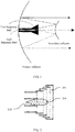
- a dual-band parabolic antenna is used in this solution, and a structure of the dual-band parabolic antenna is shown in FIG. 1 .
- the dual-band parabolic antenna includes a primary reflector, a secondary reflector, a low frequency feed, and a high frequency feed.
- the high frequency feed is inserted into the low frequency feed, and the two feeds use a same axis, and form a coaxial dual-band antenna.
- the two feeds of the coaxial dual-band antenna share the primary reflector and the secondary reflector, and phase centers of the two feeds are overlapped at a focus of the secondary reflector, so as to implement a dual-band multiplexing function.
- a low frequency feed of a coaxial dual-band antenna is usually in a shape of a large-mouth horn, and a dielectric pin needs to be inserted into a high frequency feed.
- Both the high frequency feed and the low frequency feed have problems that radiation efficiency is relatively low, and a gain cannot reach a gain level of a single-band antenna.
- Embodiments of the present application provide a coaxial dual-band antenna.
- a circular waveguide with an unchanged diameter or a circular waveguide with a small flare angle is used to replace a large-mouth horn-shaped waveguide and serves as a low frequency feed, so as to resolve problems that radiation efficiency of a high frequency feed and a low frequency feed in an existing coaxial dual-band antenna is relatively low, and a gain cannot reach a gain level of a single-band antenna.
- a coaxial dual-band antenna includes a waveguide tube, a ring groove, a high frequency feed, and a dielectric ring, where the waveguide tube has a tubular structure, and is configured to transmit a first electromagnetic wave, the ring groove whose opening direction is the same as an output direction of the first electromagnetic wave is on a wall of the waveguide tube, and a frequency of the first electromagnetic wave is lower than a frequency of an electromagnetic wave transmitted by the high frequency feed; the high frequency feed is located in the waveguide tube, and has a same axis with the waveguide tube, and the first electromagnetic wave excites a transverse electric mode TE 11 in the waveguide tube; and; and the dielectric ring is filled between the waveguide tube and the high frequency feed, the dielectric ring has a multi-layer structure, and has a same axis with the waveguide tube, area sizes of planes that are at layers of the dielectric ring and that are perpendicular to the axis alternately change, and a
- the coaxial dual-band antenna excites the TE 11 mode of the first electromagnetic wave at a low frequency, and no high order mode is generated inside the waveguide tube. This avoids a transmission loss of a high order mode in the waveguide, and improves low frequency radiation efficiency of the dual-band antenna. In addition, because no high order mode is generated inside the waveguide tube, there is no need to worry about that the high frequency feed located in the waveguide tube affects electromagnetic field distribution of the high order mode. Therefore, a dielectric pin can be omitted, and high frequency radiation efficiency of the dual-band antenna can be improved.
- a height of the high frequency feed is the same as the height of the waveguide tube.
- a sum of a radius of an inner wall of the waveguide tube and a radius of an outer wall of the high frequency feed is greater than 1/ ⁇ of a wavelength of the first electromagnetic wave, and a difference between the two radiuses is less than 1/2 of the wavelength of the first electromagnetic wave.
- a difference between a radius of the ring groove and the radius of the inner wall of the waveguide tube is 1/8 of the wavelength of the first electromagnetic wave.
- a depth of the ring groove is between 1/5 and 1/4 of the wavelength of the first electromagnetic wave, and a width of the ring groove is 1/8 of the wavelength of the first electromagnetic wave.
- Size requirements of the ring groove are provided in the foregoing two embodiments.
- a high order mode excited by a ring groove meeting the size requirements may be overlaid with the TE 11 mode, so that a beam width of the first electromagnetic wave on an E plane is consistent with that on an H plane, and radiation efficiency of the first electromagnetic wave is maximized.
- an outer wall at only one of two adjacent layers of the dielectric ring is connected to the inner wall of the waveguide tube, and an inner wall at the layer of the dielectric ring is connected to the outer wall of the high frequency feed. This can implement sealing and waterproof functions, and can fasten the high frequency feed.
- a layer that is of the dielectric ring and that is farthest from an output plane of the waveguide tube is not connected to the waveguide tube and the high frequency feed at a same time. This can reduce reflection of the first electromagnetic wave on the dielectric ring, and improve radiation efficiency.
- a height of each layer of the dielectric ring is 1/4 of the wavelength of the first electromagnetic wave.
- a relative dielectric constant of the dielectric ring is between 2 and 4.
- each layer of the dielectric ring and the relative dielectric constant are described in the foregoing two embodiments.
- the height of each layer of the dielectric ring and the relative dielectric constant enable characteristic impedance of the coaxial dual-band antenna and wave impedance of free space to match each other, and improve the radiation efficiency.
- the coaxial dual-band antenna provided in the present application excites a TE 11 mode of a first electromagnetic wave at a low frequency, and no high order mode is generated inside a waveguide tube. This avoids a transmission loss of a high order mode in the waveguide, and improves low frequency radiation efficiency of the dual-band antenna. In addition, because no high order mode is generated inside the waveguide tube, there is no need to worry about that a high frequency feed located in the waveguide tube affects electromagnetic field distribution of the high order mode. Therefore, a dielectric pin can be omitted, and high frequency radiation efficiency of the dual-band antenna can be improved.
- a structure of an existing coaxial dual-band antenna is shown in FIG. 2 .
- a low frequency feed 201 of the coaxial dual-band antenna is a large-mouth horn-shaped waveguide, a high frequency feed 202 is included in the waveguide, and a dielectric pin 203 is inserted into the high frequency feed 202.
- the horn-shaped waveguide is used to facilitate matching between characteristic impedance of the waveguide and wave impedance of free space, so as to reduce reflection.
- a radius of the waveguide increases, a high order mode is excited, and the high order mode and a transverse electric mode TE 11 take effect, so that a beam width of an output electromagnetic wave on an E plane is consistent with that on an H plane, and a best gain effect is achieved.
- the E plane is a plane including a direction in which an electric field is located and a direction with highest radiation intensity
- the H plane is a plane including a direction in which a magnetic field is located and the direction with the highest radiation intensity.
- the high order mode is generated inside the large-mouth horn-shaped waveguide, and a transmission loss in the waveguide is relatively large. Therefore, low frequency radiation efficiency of the dual-band antenna is relatively low.
- the high frequency feed is metallic, and affects electromagnetic field distribution of the high order mode. Therefore, the high frequency feed cannot directly extend to an aperture of the large-mouth horn-shaped waveguide, and a dielectric pin needs to guide a phase center of the high frequency feed to the aperture of the large-mouth horn-shaped waveguide.
- processing of the dielectric pin is uneasy, and a loss of the dielectric pin is relatively large. Therefore, a high frequency gain of the dual-band antenna cannot reach a level of a single-band antenna, either.
- the antenna includes a waveguide tube 301, a ring groove 302, a high frequency feed 303, and a dielectric ring 304.
- the waveguide tube 301 has a tubular structure, and is configured to transmit a first electromagnetic wave, the ring groove 302 whose opening direction is the same as an output direction of the first electromagnetic wave is on a wall of the waveguide tube 301, and a frequency of the first electromagnetic wave is lower than a frequency of an electromagnetic wave transmitted by the high frequency feed 303.
- the high frequency feed 303 is located in the waveguide tube 301, and has a same axis with the waveguide tube 301, and the first electromagnetic wave excites a transverse electric mode TE 11 in the waveguide tube 301.
- the dielectric ring 304 is filled between the waveguide tube 301 and the high frequency feed 303.
- the dielectric ring 304 has a multi-layer structure, and has a same axis with the waveguide tube 301. Area sizes of planes that are at layers of the dielectric ring 304 and that are perpendicular to the axis alternately change. A height of the dielectric ring 304 is less than a height of the waveguide tube 301.
- a height of the high frequency feed 303 is the same as the height of the waveguide tube 301. It should be understood that, it is also feasible if the height of the high frequency feed is slightly less than the height of the waveguide tube.
- a waveguide tube excites a TE 11 mode of a first electromagnetic wave at a low frequency, and no high order mode is generated inside the waveguide tube.
- no high order mode is generated inside the waveguide tube, there is no need to worry about that a high frequency feed located in the waveguide tube affects electromagnetic field distribution of the high order mode. Therefore, a dielectric pin can be omitted, and high frequency radiation efficiency of the dual-band antenna can be improved.
- an inner wall of the dielectric ring 304 is connected to an outer wall of the high frequency feed 303.
- an outer wall of the dielectric ring 304 may be connected to an inner wall of the waveguide tube 301; or, as shown in FIG.
- an inner wall at one or more layers of the dielectric ring 304 may be connected to an outer wall of the high frequency feed 303, and an outer wall at a remaining layer of the dielectric ring is connected to an inner wall of the waveguide tube 301.
- electromagnetic field distribution on a cross section of a waveguide is referred to as a propagation mode of the waveguide.
- Different propagation modes have different cut-off wavelengths, a mode without a cut-off wavelength or with a longest cut-off wavelength is referred to as a dominant mode or a base mode, and another mode with a shorter cut-off wavelength is referred to as a high order mode.
- a higher order of a propagation mode indicates a shorter cut-off wavelength.
- the TE 11 mode is used as the base mode, and another mode with a cut-off wavelength shorter than that of the TE 11 mode is referred to as a high order mode.
- the waveguide tube provided in this embodiment of the present application may be in a shape of a cylinder, a rectangular tube, or the like.
- a mouth for outputting the first electromagnetic wave may be slightly expanded, provided that only the base mode of the first electromagnetic wave is excited in the coaxial dual-band antenna including the waveguide tube, the high frequency feed, the ring groove, and the dielectric ring.
- a wall of the waveguide tube is usually metallic.
- a sum of a radius of the inner wall of the waveguide tube 301 and a radius of the outer wall of the high frequency feed 303 is greater than 1/ ⁇ of a wavelength of the first electromagnetic wave, a difference between the two radiuses is less than 1/2 of the wavelength of the first electromagnetic wave, and a frequency of the first electromagnetic wave is lower than a frequency of an electromagnetic wave transmitted by the high frequency feed 303.
- the coaxial waveguide including the high frequency feed 303 and the waveguide tube 301 in the present application is used as an example.
- Cut-off wavelengths of the first electromagnetic wave in different modes are related to an outer radius a of an inner waveguide (the radius of the outer wall of the high frequency feed 303) and an inner radius b of an outer waveguide (the radius of the inner wall of the waveguide tube 301) in the coaxial waveguide.
- a correspondence is listed in Table 1.
- the first electromagnetic wave may excite the TE 11 mode if the coaxial waveguide meets a condition in which (b + a) > ⁇ / ⁇ and (b - a) ⁇ ⁇ /2. If b in the coaxial waveguide becomes larger, and consequently (b - a) > ⁇ /2 and (b + a) ⁇ 2 ⁇ / ⁇ , the first electromagnetic wave may excite modes such as TE 11 , TM m1 , and TE 01 in theory.
- modes such as TE 11 , TM m1 , and TE 01 in theory.
- a continuous tangential component needs to be ensured when an electromagnetic field mode changes, that is, m needs to be consistent. Therefore, only two modes actually exist: TE 11 and TM 11 . As the inner radius b of the outer waveguide in the coaxial waveguide increases, more modes exist gradually.
- a transverse electromagnetic mode TEM may also exist in the coaxial waveguide, and no cut-off wavelength exists in this mode or a cut-off wavelength in this mode is infinitely long.
- the TEM mode is suppressed in a symmetrical feeding manner. Therefore, this mode is not considered in this embodiment of the present application.
- the ring groove 302 whose opening direction is the same as the output direction of the first electromagnetic wave is excavated on the wall of the waveguide tube 301, a high order mode is excited by using discontinuity of the wall of the waveguide tube 301, and the high order mode is used to make the electric field distribution of the TE 11 mode become uniform.
- a depth and a width of the ring groove 302 and a distance from the ring groove 302 to the inner wall of the waveguide tube 301 all affect an order and amplitude of the high order mode.
- a difference between a radius of the ring groove 302 and the radius of the inner wall of the waveguide tube 301 is 1/8 of the wavelength of the first electromagnetic wave.
- the depth of the ring groove 302 is between 1/5 and 1/4 of the wavelength of the first electromagnetic wave, and the width of the ring groove 302 is 1/8 of the wavelength of the first electromagnetic wave.
- the ring groove 302 causes discontinuity on a surface of the wall, so that the high order mode is excited.
- the location, the width, and the depth of the ring groove 302 meet the foregoing requirements, so that the high order mode TM 11 with an appropriate amplitude can be generated.
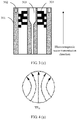
- Electric field distribution of the TM 11 mode is shown in FIG. 4 (b) .
- FIG. 4 (c) the TE 11 mode and the TM 11 mode are overlaid, so that the electric field distribution of the first electromagnetic wave becomes uniform. Consequently, the beam width of the first electromagnetic wave on the E plane is consistent with that on the H plane, and a gain effect is maximized.
- impedance matching may be implemented in the following two manners.
- the dielectric ring 304 filled between the waveguide tube 301 and the high frequency feed 303 is used to implement impedance matching.
- the dielectric ring 304 has the multi-layer structure, and has the same axis with the waveguide tube 301.
- the area sizes of the planes that are at the layers of the dielectric ring 304 and that are perpendicular to the axis alternately change.
- the height of the dielectric ring 304 is less than the height of the waveguide tube 301.
- the structure of the dielectric ring 304 may be any structure shown in FIG. 3 (a), FIG. 3 (b) , and FIG. 3 (c) .
- R 0 is the characteristic impedance of the waveguide
- R L is the load impedance
- the load impedance is the wave impedance of the free space
- the characteristic impedance of the waveguide is the characteristic impedance of the coaxial dual-band antenna.
- the characteristic impedance of the waveguide tube can be changed by filling a dielectric in the waveguide tube. That is, the filled dielectric ring forms the matching section.
- the waveguide tube is fully filled with the dielectric, in the waveguide tube, a sudden change of the characteristic impedance occurs on a contact surface between the dielectric and the air, and there is strong reflection.
- the dielectric ring 304 used in the present application does not fully fill a gap between the waveguide tube 301 and the high frequency feed 303, but uses the multi-layer structure having the same axis with the waveguide tube 301.
- the area sizes of the planes that are at the layers of the dielectric ring 304 and that are perpendicular to the axis alternately change, to form a mixture of the dielectric and the air. Therefore, an equivalent relative dielectric constant is no longer equal to a relative dielectric constant of a material, and can be controlled and changed.
- a purpose of such control and change is to enable the characteristic impedance of the matching section to reach a value obtained by means of calculation by using the foregoing formula.
- a height of each layer of the dielectric ring 304 is 1/4 of the wavelength of the first electromagnetic wave, and the first electromagnetic wave is a low frequency electromagnetic wave transmitted by the coaxial dual-band antenna.
- an outer wall at only one of two adjacent layers of the dielectric ring 304 is connected to the inner wall of the waveguide tube 301, and an inner wall at the layer of the dielectric ring 304 is connected to the outer wall of the high frequency feed 303.
- inner walls at multiple layers of the dielectric ring 304 are connected to the outer wall of the high frequency feed 303, and outer walls at the multiple layers of the dielectric ring 304 are connected to the inner wall of the waveguide tube 301.
- This can implement air sealing and waterproof functions, and can fasten the high frequency feed 303 in between.
- the coaxial dual-band antenna not only can be applied to satellite communication, but also is applicable to the ground.
- spacing between an inner wall and an outer wall at another layer of the dielectric ring 304 needs to be designed and optimized according to the foregoing equivalent dielectric constant principle.
- a layer that is of the dielectric ring 304 and that is farthest from an output plane of the waveguide tube 301 is not connected to the waveguide tube 301 and the high frequency feed 303 at a same time, so as to reduce reflection of the first electromagnetic wave.
- the layer that is of the dielectric ring and that is farthest from the output plane is a bottom layer of the dielectric ring shown in FIG. 5 (a) and FIG. 5 (b) .
- a dielectric material whose relative dielectric constant is between 2 and 4 may be used for the dielectric ring in this embodiment of the present application, for example, polycarbonate, polystyrene, and polytetrafluorethylene.
- a specific material is not limited in this embodiment of the present application.
- spacing between an inner wall and an outer wall at each layer of the dielectric ring 304 is further related to the wavelength of the first electromagnetic wave.
- the following provides a specific embodiment in which the frequency of the first electromagnetic wave is 18 GHz. It is assumed that polycarbonate whose relative dielectric constant is 2.8 is used to prepare the dielectric ring, the radius of the inner wall of the waveguide tube is R, and the dielectric ring has six layers. As shown in FIG.
- radius lengths of layers of the dielectric ring alternately change from top to bottom, radiuses of outer walls at the first layer, the third layer, and the fifth layer of the dielectric ring are R, a radius of an outer wall at the second layer of the dielectric ring is 0.78R, a radius of an outer wall at the fourth layer of the dielectric ring is 0.7R, and a radius of an outer wall at the sixth layer of the dielectric ring is 0.7R.
- the characteristic impedance of the matching section can meet formula (1) by using the dielectric ring with the foregoing sizes, so that the characteristic impedance of the coaxial dual-band antenna and the wave impedance of the free space match each other, electromagnetic wave reflection is reduced, and radiation efficiency is improved.
- each metal ring 601 is disposed in the waveguide tube to implement impedance matching.
- the metal rings form a matching section.
- a possible structure is shown in FIG. 6 (a) , and an inner wall of each metal ring 601 is connected to the outer wall of the high frequency feed 303.
- Equivalent inductance and equivalent capacitance of each metal ring 601 may be changed by changing a radius of each metal ring 601 and spacing between the metal rings 601, so that characteristic impedance of the matching section reaches a value obtained by means of calculation by using formula (1).
- a dielectric layer 602 may further be filled at a location that is inside the waveguide tube 301 and that is close to the output plane. As shown in FIG. 6 (b) , an inner wall of the dielectric layer 602 is connected to the outer wall of the high frequency feed 303, and an outer wall of the dielectric layer 602 is connected to the inner wall of the waveguide tube 301. This can implement air sealing and waterproof functions, and can fasten the high frequency feed.
- a hard material may be used for the dielectric layer 602, and a specific material is not limited in the present application.
- FIG. 6 (a) and FIG. 6 (b) show only possible structures in this embodiment of the present application.
- outer walls of the metal rings 601 may be connected to the inner wall of the waveguide tube 301, to form a matching section.
- outer walls of some metal rings 601 are connected to the inner wall of the waveguide tube 301, and inner walls of the other part of metal rings 601 are connected to the outer wall of the high frequency feed 303, to form a matching section.
- a specific implementation is not limited in this embodiment of the present application.
- the coaxial dual-band antenna provided in the present application has the following advantages: A waveguide tube 301 excites a TE 11 mode of a first electromagnetic wave at a low frequency, and no high order mode is generated inside the waveguide tube 301. This avoids a transmission loss of a high order mode in the waveguide tube 301, and improves low frequency radiation efficiency of the dual-band antenna. In addition, because no high order mode is generated inside the waveguide tube 301, there is no need to worry about that a high frequency feed 303 located in the waveguide tube 301 affects electromagnetic field distribution of the high order mode. Therefore, a dielectric pin can be omitted, and high frequency radiation efficiency of the dual-band antenna can be improved.
- a beam width of the first electromagnetic wave on an E plane can be consistent with that on an H plane, and characteristic impedance of the coaxial dual-band antenna and wave impedance of free space can match each other.
- Embodiment 1 A coaxial dual-band antenna, comprising: a waveguide tube, a ring groove, a high frequency feed, and a dielectric ring, wherein the waveguide tube has a tubular structure, and is configured to transmit a first electromagnetic wave, the ring groove whose opening direction is the same as an output direction of the first electromagnetic wave is on a wall of the waveguide tube, and a frequency of the first electromagnetic wave is lower than a frequency of an electromagnetic wave transmitted by the high frequency feed; the high frequency feed is located in the waveguide tube, and has a same axis with the waveguide tube, and the first electromagnetic wave excites a transverse electric mode TE 11 in the waveguide tube; and the dielectric ring is filled between the waveguide tube and the high frequency feed, the dielectric ring has a multi-layer structure, and has a same axis with the waveguide tube, area sizes of planes that are at layers of the dielectric ring and that are perpendicular to the axis alternately change, and a height of the
- Embodiment 2 The antenna according to embodiment 1, wherein a height of the high frequency feed is the same as the height of the waveguide tube.
- Embodiment 3 The antenna according to embodiment 1, wherein a sum of a radius of an inner wall of the waveguide tube and a radius of an outer wall of the high frequency feed is greater than 1/ ⁇ of a wavelength of the first electromagnetic wave, and a difference between the two radiuses is less than 1/2 of the wavelength of the first electromagnetic wave.
- Embodiment 4 The antenna according to any one of embodiments 1 to 3, wherein a difference between a radius of the ring groove and the radius of the inner wall of the waveguide tube is 1/8 of the wavelength of the first electromagnetic wave.
- Embodiment 5 The antenna according to embodiment 4, wherein a depth of the ring groove is between 1/5 and 1/4 of the wavelength of the first electromagnetic wave, and a width of the ring groove is 1/8 of the wavelength of the first electromagnetic wave.
- Embodiment 6 The antenna according to any one of embodiments 1 to 3, wherein an outer wall at only one of two adjacent layers of the dielectric ring is connected to the inner wall of the waveguide tube, and an inner wall at the layer of the dielectric ring is connected to the outer wall of the high frequency feed.
- Embodiment 7 The antenna according to embodiment 6, wherein a layer that is of the dielectric ring and that is farthest from an output plane of the waveguide tube is not connected to the waveguide tube and the high frequency feed at a same time.
- Embodiment 8 The antenna according to embodiment 6, wherein a height of each layer of the dielectric ring is 1/4 of the wavelength of the first electromagnetic wave.
- Embodiment 9 The antenna according to embodiment 6, wherein a relative dielectric constant of the dielectric ring is between 2 and 4.
Landscapes
- Physics & Mathematics (AREA)
- Electromagnetism (AREA)
- Waveguide Aerials (AREA)
Abstract
Description
- The present application relates to the field of wireless communications, and in particular, to a coaxial dual-band antenna that can be used in a dual-band parabolic antenna.
- With rapid development of wireless communications technologies, a transmission capacity in microwave point-to-point communication continuously increases, and an E-band (71 to 76 GHz, 81 to 86 GHz) frequency band microwave device plays an increasingly important role in a base station backhaul network. However, because "rain fade" on an E-band frequency band electromagnetic wave is extremely severe, an E-band microwave single-hop distance is usually less than 3 kilometers. To increase the E-band microwave single-hop distance and reduce site deployment costs, a solution is provided, in which the E-band frequency band microwave device and another low frequency microwave device are cooperatively used. When there is relatively heavy rain, even if the E-band microwave device cannot normally work, the low frequency microwave device can still normally work.
- A dual-band parabolic antenna is used in this solution, and a structure of the dual-band parabolic antenna is shown in
FIG. 1 . The dual-band parabolic antenna includes a primary reflector, a secondary reflector, a low frequency feed, and a high frequency feed. The high frequency feed is inserted into the low frequency feed, and the two feeds use a same axis, and form a coaxial dual-band antenna. The two feeds of the coaxial dual-band antenna share the primary reflector and the secondary reflector, and phase centers of the two feeds are overlapped at a focus of the secondary reflector, so as to implement a dual-band multiplexing function. - In the prior art, a low frequency feed of a coaxial dual-band antenna is usually in a shape of a large-mouth horn, and a dielectric pin needs to be inserted into a high frequency feed. Both the high frequency feed and the low frequency feed have problems that radiation efficiency is relatively low, and a gain cannot reach a gain level of a single-band antenna.
- Embodiments of the present application provide a coaxial dual-band antenna. A circular waveguide with an unchanged diameter or a circular waveguide with a small flare angle is used to replace a large-mouth horn-shaped waveguide and serves as a low frequency feed, so as to resolve problems that radiation efficiency of a high frequency feed and a low frequency feed in an existing coaxial dual-band antenna is relatively low, and a gain cannot reach a gain level of a single-band antenna.
- According to a first aspect, a coaxial dual-band antenna is provided and includes a waveguide tube, a ring groove, a high frequency feed, and a dielectric ring, where the waveguide tube has a tubular structure, and is configured to transmit a first electromagnetic wave, the ring groove whose opening direction is the same as an output direction of the first electromagnetic wave is on a wall of the waveguide tube, and a frequency of the first electromagnetic wave is lower than a frequency of an electromagnetic wave transmitted by the high frequency feed; the high frequency feed is located in the waveguide tube, and has a same axis with the waveguide tube, and the first electromagnetic wave excites a transverse electric mode TE11 in the waveguide tube; and; and the dielectric ring is filled between the waveguide tube and the high frequency feed, the dielectric ring has a multi-layer structure, and has a same axis with the waveguide tube, area sizes of planes that are at layers of the dielectric ring and that are perpendicular to the axis alternately change, and a height of the dielectric ring is less than a height of the waveguide tube.
- The coaxial dual-band antenna provided in the embodiments of the present application excites the TE11 mode of the first electromagnetic wave at a low frequency, and no high order mode is generated inside the waveguide tube. This avoids a transmission loss of a high order mode in the waveguide, and improves low frequency radiation efficiency of the dual-band antenna. In addition, because no high order mode is generated inside the waveguide tube, there is no need to worry about that the high frequency feed located in the waveguide tube affects electromagnetic field distribution of the high order mode. Therefore, a dielectric pin can be omitted, and high frequency radiation efficiency of the dual-band antenna can be improved.
- With reference to the first aspect, in a first possible implementation of the first aspect, a height of the high frequency feed is the same as the height of the waveguide tube.
- With reference to the first aspect, in a second possible implementation of the first aspect, a sum of a radius of an inner wall of the waveguide tube and a radius of an outer wall of the high frequency feed is greater than 1/π of a wavelength of the first electromagnetic wave, and a difference between the two radiuses is less than 1/2 of the wavelength of the first electromagnetic wave. In the embodiments, it can be ensured that only the TE11 mode is exited in the antenna, and a mode of a higher order does not exist, and therefore, a transmission loss of a high order mode in a waveguide is avoided.
- With reference to the first aspect, or the first or the second possible implementation of the first aspect, in a third possible implementation of the first aspect, a difference between a radius of the ring groove and the radius of the inner wall of the waveguide tube is 1/8 of the wavelength of the first electromagnetic wave.
- With reference to the third possible implementation of the first aspect, in a fourth possible implementation of the first aspect, a depth of the ring groove is between 1/5 and 1/4 of the wavelength of the first electromagnetic wave, and a width of the ring groove is 1/8 of the wavelength of the first electromagnetic wave.
- Size requirements of the ring groove are provided in the foregoing two embodiments. A high order mode excited by a ring groove meeting the size requirements may be overlaid with the TE11 mode, so that a beam width of the first electromagnetic wave on an E plane is consistent with that on an H plane, and radiation efficiency of the first electromagnetic wave is maximized.
- With reference to any one of the first aspect, or the first to the fourth possible implementations of the first aspect, in a fifth possible implementation of the first aspect, an outer wall at only one of two adjacent layers of the dielectric ring is connected to the inner wall of the waveguide tube, and an inner wall at the layer of the dielectric ring is connected to the outer wall of the high frequency feed. This can implement sealing and waterproof functions, and can fasten the high frequency feed.
- With reference to any one of the first aspect, or the first to the fifth possible implementations of the first aspect, in a sixth possible implementation of the first aspect, a layer that is of the dielectric ring and that is farthest from an output plane of the waveguide tube is not connected to the waveguide tube and the high frequency feed at a same time. This can reduce reflection of the first electromagnetic wave on the dielectric ring, and improve radiation efficiency.
- With reference to the sixth possible implementation of the first aspect, in a seventh possible implementation of the first aspect, a height of each layer of the dielectric ring is 1/4 of the wavelength of the first electromagnetic wave.
- With reference to the sixth or the seventh possible implementation of the first aspect, in an eighth possible implementation of the first aspect, a relative dielectric constant of the dielectric ring is between 2 and 4.
- The height of each layer of the dielectric ring and the relative dielectric constant are described in the foregoing two embodiments. The height of each layer of the dielectric ring and the relative dielectric constant enable characteristic impedance of the coaxial dual-band antenna and wave impedance of free space to match each other, and improve the radiation efficiency.
- The coaxial dual-band antenna provided in the present application excites a TE11 mode of a first electromagnetic wave at a low frequency, and no high order mode is generated inside a waveguide tube. This avoids a transmission loss of a high order mode in the waveguide, and improves low frequency radiation efficiency of the dual-band antenna. In addition, because no high order mode is generated inside the waveguide tube, there is no need to worry about that a high frequency feed located in the waveguide tube affects electromagnetic field distribution of the high order mode. Therefore, a dielectric pin can be omitted, and high frequency radiation efficiency of the dual-band antenna can be improved.
-
-
FIG. 1 is a schematic structural diagram of an existing dual-band parabolic antenna; -
FIG. 2 is a schematic structural diagram of an existing coaxial dual-band antenna; -
FIG. 3 (a) is a schematic structural diagram of a coaxial dual-band antenna according to an embodiment of the present application; -
FIG. 3 (b) is a schematic structural diagram of a coaxial dual-band antenna according to another embodiment of the present application; -
FIG. 3 (c) is a schematic structural diagram of a coaxial dual-band antenna according to another embodiment of the present application; -
FIG. 4 (a) is a distribution diagram of an electric field of a TE11 mode in a coaxial dual-band antenna according to an embodiment of the present application; -
FIG. 4 (b) is a distribution diagram of an electric field of a TM11 mode in a coaxial dual-band antenna according to an embodiment of the present application; -
FIG. 4 (c) is a distribution diagram of an electric field obtained after a TE11 mode and a TM11 mode in a coaxial dual-band antenna are overlaid according to an embodiment of the present application; -
FIG. 5 (a) is a schematic structural diagram of a coaxial dual-band antenna according to another embodiment of the present application; -
FIG. 5 (b) is a schematic structural diagram of a coaxial dual-band antenna according to another embodiment of the present application; -
FIG. 6 (a) is a schematic structural diagram of a coaxial dual-band antenna according to another embodiment of the present application; -
FIG. 6 (b) is a schematic structural diagram of a coaxial dual-band antenna according to another embodiment of the present application; -
FIG. 7 (a) is a schematic structural diagram of a coaxial dual-band antenna according to another embodiment of the present application; -
FIG. 7 (b) is a schematic structural diagram of a coaxial dual-band antenna according to another embodiment of the present application; -
FIG. 8 (a) is a schematic structural diagram of a coaxial dual-band antenna according to another embodiment of the present application; and -
FIG. 8 (b) is a schematic structural diagram of a coaxial dual-band antenna according to another embodiment of the present application. - The following describes the technical solutions in the embodiments of this application with reference to the accompanying drawings in the embodiments of this application.
- A structure of an existing coaxial dual-band antenna is shown in
FIG. 2 . Alow frequency feed 201 of the coaxial dual-band antenna is a large-mouth horn-shaped waveguide, ahigh frequency feed 202 is included in the waveguide, and adielectric pin 203 is inserted into thehigh frequency feed 202. The horn-shaped waveguide is used to facilitate matching between characteristic impedance of the waveguide and wave impedance of free space, so as to reduce reflection. As a radius of the waveguide increases, a high order mode is excited, and the high order mode and a transverse electric mode TE11 take effect, so that a beam width of an output electromagnetic wave on an E plane is consistent with that on an H plane, and a best gain effect is achieved. The E plane is a plane including a direction in which an electric field is located and a direction with highest radiation intensity, and the H plane is a plane including a direction in which a magnetic field is located and the direction with the highest radiation intensity. However, the high order mode is generated inside the large-mouth horn-shaped waveguide, and a transmission loss in the waveguide is relatively large. Therefore, low frequency radiation efficiency of the dual-band antenna is relatively low. - The high frequency feed is metallic, and affects electromagnetic field distribution of the high order mode. Therefore, the high frequency feed cannot directly extend to an aperture of the large-mouth horn-shaped waveguide, and a dielectric pin needs to guide a phase center of the high frequency feed to the aperture of the large-mouth horn-shaped waveguide. However, processing of the dielectric pin is uneasy, and a loss of the dielectric pin is relatively large. Therefore, a high frequency gain of the dual-band antenna cannot reach a level of a single-band antenna, either.
- An embodiment of the present application provides a coaxial dual-band antenna. As shown in
FIG. 3 (a) , the antenna includes awaveguide tube 301, aring groove 302, ahigh frequency feed 303, and adielectric ring 304. - The
waveguide tube 301 has a tubular structure, and is configured to transmit a first electromagnetic wave, thering groove 302 whose opening direction is the same as an output direction of the first electromagnetic wave is on a wall of thewaveguide tube 301, and a frequency of the first electromagnetic wave is lower than a frequency of an electromagnetic wave transmitted by thehigh frequency feed 303. - The
high frequency feed 303 is located in thewaveguide tube 301, and has a same axis with thewaveguide tube 301, and the first electromagnetic wave excites a transverse electric mode TE11 in thewaveguide tube 301. - The
dielectric ring 304 is filled between thewaveguide tube 301 and thehigh frequency feed 303. Thedielectric ring 304 has a multi-layer structure, and has a same axis with thewaveguide tube 301. Area sizes of planes that are at layers of thedielectric ring 304 and that are perpendicular to the axis alternately change. A height of thedielectric ring 304 is less than a height of thewaveguide tube 301. - Optionally, a height of the
high frequency feed 303 is the same as the height of thewaveguide tube 301. It should be understood that, it is also feasible if the height of the high frequency feed is slightly less than the height of the waveguide tube. - In this embodiment of the present application, a waveguide tube excites a TE11 mode of a first electromagnetic wave at a low frequency, and no high order mode is generated inside the waveguide tube. This avoids a transmission loss of a high order mode in the waveguide, and improves low frequency radiation efficiency of a dual-band antenna. In addition, because no high order mode is generated inside the waveguide tube, there is no need to worry about that a high frequency feed located in the waveguide tube affects electromagnetic field distribution of the high order mode. Therefore, a dielectric pin can be omitted, and high frequency radiation efficiency of the dual-band antenna can be improved.
- It should be understood that, in the coaxial dual-band antenna shown in
FIG. 3 (a) , an inner wall of thedielectric ring 304 is connected to an outer wall of thehigh frequency feed 303. This is only a possible structure of the coaxial dual-band antenna provided in the present application. Provided that area sizes of planes that are at layers of thedielectric ring 304 and that are perpendicular to the axis alternately change, alternatively, as shown inFIG. 3 (b) , in the antenna, an outer wall of thedielectric ring 304 may be connected to an inner wall of thewaveguide tube 301; or, as shown inFIG. 3 (c) , an inner wall at one or more layers of thedielectric ring 304 may be connected to an outer wall of thehigh frequency feed 303, and an outer wall at a remaining layer of the dielectric ring is connected to an inner wall of thewaveguide tube 301. - It should be noted that, electromagnetic field distribution on a cross section of a waveguide is referred to as a propagation mode of the waveguide. Different propagation modes have different cut-off wavelengths, a mode without a cut-off wavelength or with a longest cut-off wavelength is referred to as a dominant mode or a base mode, and another mode with a shorter cut-off wavelength is referred to as a high order mode. A higher order of a propagation mode indicates a shorter cut-off wavelength. In this embodiment of the present application, the TE11 mode is used as the base mode, and another mode with a cut-off wavelength shorter than that of the TE11 mode is referred to as a high order mode.
- It should be understood that, the waveguide tube provided in this embodiment of the present application may be in a shape of a cylinder, a rectangular tube, or the like. A mouth for outputting the first electromagnetic wave may be slightly expanded, provided that only the base mode of the first electromagnetic wave is excited in the coaxial dual-band antenna including the waveguide tube, the high frequency feed, the ring groove, and the dielectric ring. A wall of the waveguide tube is usually metallic.
- Optionally, a sum of a radius of the inner wall of the
waveguide tube 301 and a radius of the outer wall of thehigh frequency feed 303 is greater than 1/π of a wavelength of the first electromagnetic wave, a difference between the two radiuses is less than 1/2 of the wavelength of the first electromagnetic wave, and a frequency of the first electromagnetic wave is lower than a frequency of an electromagnetic wave transmitted by thehigh frequency feed 303. - Specifically, the coaxial waveguide including the
high frequency feed 303 and thewaveguide tube 301 in the present application is used as an example. Cut-off wavelengths of the first electromagnetic wave in different modes are related to an outer radius a of an inner waveguide (the radius of the outer wall of the high frequency feed 303) and an inner radius b of an outer waveguide (the radius of the inner wall of the waveguide tube 301) in the coaxial waveguide. A correspondence is listed in Table 1.Table 1 Propagation mode Cut-off wavelength TEM No cut-off wavelength TE11 π×(b+a) TMm1 (m=0, 1, 2...), TE01 2×(b-a) TE21 π×(b+a)/2 TEm1 (m=3, 4, 5...) π×(b+a)/m TMm2, TE02 b-a TMmn (n=3, 4, 5...), TE0n (n=3, 4, 5...) 2×(b-a)/n - If the wavelength of the first electromagnetic wave is λ, it can be learned from Table 1 that, the first electromagnetic wave may excite the TE11 mode if the coaxial waveguide meets a condition in which (b + a) > λ/π and (b - a) < λ/2. If b in the coaxial waveguide becomes larger, and consequently (b - a) > λ/2 and (b + a) < 2λ/π, the first electromagnetic wave may excite modes such as TE11, TMm1, and TE01 in theory. However, a continuous tangential component needs to be ensured when an electromagnetic field mode changes, that is, m needs to be consistent. Therefore, only two modes actually exist: TE11 and TM11. As the inner radius b of the outer waveguide in the coaxial waveguide increases, more modes exist gradually.
- It should be noted that, a transverse electromagnetic mode TEM may also exist in the coaxial waveguide, and no cut-off wavelength exists in this mode or a cut-off wavelength in this mode is infinitely long. However, before being excited in the coaxial dual-band antenna, the TEM mode is suppressed in a symmetrical feeding manner. Therefore, this mode is not considered in this embodiment of the present application.
- Further, as shown in
FIG. 4 (a) , only the TE11 mode exists in the waveguide tube, and electric field distribution of the TE11 mode in the waveguide tube is non-uniform, that is, electric field distribution of the first electromagnetic wave is non-uniform. Therefore, a beam width of the first electromagnetic wave on the E plane is inconsistent with that on the H plane. For the foregoing problem, in this embodiment of the present application, thering groove 302 whose opening direction is the same as the output direction of the first electromagnetic wave is excavated on the wall of thewaveguide tube 301, a high order mode is excited by using discontinuity of the wall of thewaveguide tube 301, and the high order mode is used to make the electric field distribution of the TE11 mode become uniform. A depth and a width of thering groove 302 and a distance from thering groove 302 to the inner wall of thewaveguide tube 301 all affect an order and amplitude of the high order mode. - Optionally, a difference between a radius of the
ring groove 302 and the radius of the inner wall of thewaveguide tube 301 is 1/8 of the wavelength of the first electromagnetic wave. The depth of thering groove 302 is between 1/5 and 1/4 of the wavelength of the first electromagnetic wave, and the width of thering groove 302 is 1/8 of the wavelength of the first electromagnetic wave. Specifically, at a location that is on a wall plane at an output end of the waveguide tube and whose distance with the inner wall of the waveguide tube is 1/8 of the wavelength of the first electromagnetic wave, a ring whose width and depth meet the foregoing requirements is excavated on the wall, to form thering groove 302. Thering groove 302 causes discontinuity on a surface of the wall, so that the high order mode is excited. The location, the width, and the depth of thering groove 302 meet the foregoing requirements, so that the high order mode TM11 with an appropriate amplitude can be generated. Electric field distribution of the TM11 mode is shown inFIG. 4 (b) . As shown inFIG. 4 (c) , the TE11 mode and the TM11 mode are overlaid, so that the electric field distribution of the first electromagnetic wave becomes uniform. Consequently, the beam width of the first electromagnetic wave on the E plane is consistent with that on the H plane, and a gain effect is maximized. - In addition, a large-mouth horn-shaped waveguide is omitted in this embodiment of the present application. Therefore, characteristic impedance of the coaxial dual-band antenna and wave impedance of free space cannot match each other by gradually changing the characteristic impedance at the output end of the waveguide tube by using a gradually increasing diameter of the waveguide tube. In this embodiment of the present application, impedance matching may be implemented in the following two manners.
- (1) The
dielectric ring 304 filled between thewaveguide tube 301 and thehigh frequency feed 303 is used to implement impedance matching. Thedielectric ring 304 has the multi-layer structure, and has the same axis with thewaveguide tube 301. The area sizes of the planes that are at the layers of thedielectric ring 304 and that are perpendicular to the axis alternately change. The height of thedielectric ring 304 is less than the height of thewaveguide tube 301. The structure of thedielectric ring 304 may be any structure shown inFIG. 3 (a), FIG. 3 (b) , andFIG. 3 (c) . - According to an impedance matching principle, when load impedance and characteristic impedance of a waveguide are inconsistent, to ensure that energy is transferred to a load and is not reflected back, a matching section is required between the load and the waveguide. When characteristic impedance Z0 of the matching section meets the following formula, the characteristic impedance of the waveguide is equal to the load impedance after being converted by the matching section.

- R0 is the characteristic impedance of the waveguide, and RL is the load impedance.
- In this embodiment of the present invention, the load impedance is the wave impedance of the free space, and the characteristic impedance of the waveguide is the characteristic impedance of the coaxial dual-band antenna. The characteristic impedance of the waveguide tube can be changed by filling a dielectric in the waveguide tube. That is, the filled dielectric ring forms the matching section. However, if the waveguide tube is fully filled with the dielectric, in the waveguide tube, a sudden change of the characteristic impedance occurs on a contact surface between the dielectric and the air, and there is strong reflection.
- The
dielectric ring 304 used in the present application does not fully fill a gap between thewaveguide tube 301 and thehigh frequency feed 303, but uses the multi-layer structure having the same axis with thewaveguide tube 301. The area sizes of the planes that are at the layers of thedielectric ring 304 and that are perpendicular to the axis alternately change, to form a mixture of the dielectric and the air. Therefore, an equivalent relative dielectric constant is no longer equal to a relative dielectric constant of a material, and can be controlled and changed. A purpose of such control and change is to enable the characteristic impedance of the matching section to reach a value obtained by means of calculation by using the foregoing formula. - Optionally, a height of each layer of the
dielectric ring 304 is 1/4 of the wavelength of the first electromagnetic wave, and the first electromagnetic wave is a low frequency electromagnetic wave transmitted by the coaxial dual-band antenna. - Optionally, in a structure shown in
FIG. 5 (a) or FIG. 5 (b) , an outer wall at only one of two adjacent layers of thedielectric ring 304 is connected to the inner wall of thewaveguide tube 301, and an inner wall at the layer of thedielectric ring 304 is connected to the outer wall of thehigh frequency feed 303. In this way, inner walls at multiple layers of thedielectric ring 304 are connected to the outer wall of thehigh frequency feed 303, and outer walls at the multiple layers of thedielectric ring 304 are connected to the inner wall of thewaveguide tube 301. This can implement air sealing and waterproof functions, and can fasten thehigh frequency feed 303 in between. Consequently, the coaxial dual-band antenna not only can be applied to satellite communication, but also is applicable to the ground. Other than the layers of the dielectric ring that are connected to both thewaveguide tube 301 and thehigh frequency feed 303, spacing between an inner wall and an outer wall at another layer of thedielectric ring 304 needs to be designed and optimized according to the foregoing equivalent dielectric constant principle. - Optionally, a layer that is of the
dielectric ring 304 and that is farthest from an output plane of thewaveguide tube 301 is not connected to thewaveguide tube 301 and thehigh frequency feed 303 at a same time, so as to reduce reflection of the first electromagnetic wave. The layer that is of the dielectric ring and that is farthest from the output plane is a bottom layer of the dielectric ring shown inFIG. 5 (a) and FIG. 5 (b) . - A dielectric material whose relative dielectric constant is between 2 and 4 may be used for the dielectric ring in this embodiment of the present application, for example, polycarbonate, polystyrene, and polytetrafluorethylene. A specific material is not limited in this embodiment of the present application.
- After the material is determined, spacing between an inner wall and an outer wall at each layer of the
dielectric ring 304 is further related to the wavelength of the first electromagnetic wave. The following provides a specific embodiment in which the frequency of the first electromagnetic wave is 18 GHz. It is assumed that polycarbonate whose relative dielectric constant is 2.8 is used to prepare the dielectric ring, the radius of the inner wall of the waveguide tube is R, and the dielectric ring has six layers. As shown inFIG. 5 (a) , radius lengths of layers of the dielectric ring alternately change from top to bottom, radiuses of outer walls at the first layer, the third layer, and the fifth layer of the dielectric ring are R, a radius of an outer wall at the second layer of the dielectric ring is 0.78R, a radius of an outer wall at the fourth layer of the dielectric ring is 0.7R, and a radius of an outer wall at the sixth layer of the dielectric ring is 0.7R. The characteristic impedance of the matching section can meet formula (1) by using the dielectric ring with the foregoing sizes, so that the characteristic impedance of the coaxial dual-band antenna and the wave impedance of the free space match each other, electromagnetic wave reflection is reduced, and radiation efficiency is improved. - (2) Multiple metal rings 601 are disposed in the waveguide tube to implement impedance matching. The metal rings form a matching section. A possible structure is shown in
FIG. 6 (a) , and an inner wall of eachmetal ring 601 is connected to the outer wall of thehigh frequency feed 303. Equivalent inductance and equivalent capacitance of eachmetal ring 601 may be changed by changing a radius of eachmetal ring 601 and spacing between the metal rings 601, so that characteristic impedance of the matching section reaches a value obtained by means of calculation by using formula (1). - Optionally, a
dielectric layer 602 may further be filled at a location that is inside thewaveguide tube 301 and that is close to the output plane. As shown inFIG. 6 (b) , an inner wall of thedielectric layer 602 is connected to the outer wall of thehigh frequency feed 303, and an outer wall of thedielectric layer 602 is connected to the inner wall of thewaveguide tube 301. This can implement air sealing and waterproof functions, and can fasten the high frequency feed. A hard material may be used for thedielectric layer 602, and a specific material is not limited in the present application. - It should be understood that,
FIG. 6 (a) and FIG. 6 (b) show only possible structures in this embodiment of the present application. As shown inFIG. 7(a) and FIG. 7(b) , outer walls of the metal rings 601 may be connected to the inner wall of thewaveguide tube 301, to form a matching section. Alternatively, as shown inFIG. 8 (a) and FIG. 8 (b) , outer walls of some metal rings 601 are connected to the inner wall of thewaveguide tube 301, and inner walls of the other part of metal rings 601 are connected to the outer wall of thehigh frequency feed 303, to form a matching section. A specific implementation is not limited in this embodiment of the present application. - The coaxial dual-band antenna provided in the present application has the following advantages: A
waveguide tube 301 excites a TE11 mode of a first electromagnetic wave at a low frequency, and no high order mode is generated inside thewaveguide tube 301. This avoids a transmission loss of a high order mode in thewaveguide tube 301, and improves low frequency radiation efficiency of the dual-band antenna. In addition, because no high order mode is generated inside thewaveguide tube 301, there is no need to worry about that ahigh frequency feed 303 located in thewaveguide tube 301 affects electromagnetic field distribution of the high order mode. Therefore, a dielectric pin can be omitted, and high frequency radiation efficiency of the dual-band antenna can be improved. In addition, according to a design of aring groove 302 and adielectric ring 304, a beam width of the first electromagnetic wave on an E plane can be consistent with that on an H plane, and characteristic impedance of the coaxial dual-band antenna and wave impedance of free space can match each other. - The foregoing descriptions are merely specific implementations of this application, but are not intended to limit the protection scope of this application. Any variation or replacement readily figured out by a person skilled in the art within the technical scope disclosed in this application shall fall within the protection scope of this application. Therefore, the protection scope of this application shall be subject to the protection scope of the claims.
- Further embodiments of the present invention are provided in the following. It should be noted that the numbering used in the following section does not necessarily need to comply with the numbering used in the previous sections.
- Embodiment 1. A coaxial dual-band antenna, comprising: a waveguide tube, a ring groove, a high frequency feed, and a dielectric ring, wherein
the waveguide tube has a tubular structure, and is configured to transmit a first electromagnetic wave, the ring groove whose opening direction is the same as an output direction of the first electromagnetic wave is on a wall of the waveguide tube, and a frequency of the first electromagnetic wave is lower than a frequency of an electromagnetic wave transmitted by the high frequency feed;
the high frequency feed is located in the waveguide tube, and has a same axis with the waveguide tube, and the first electromagnetic wave excites a transverse electric mode TE11 in the waveguide tube; and
the dielectric ring is filled between the waveguide tube and the high frequency feed, the dielectric ring has a multi-layer structure, and has a same axis with the waveguide tube, area sizes of planes that are at layers of the dielectric ring and that are perpendicular to the axis alternately change, and a height of the dielectric ring is less than a height of the waveguide tube. - Embodiment 2. The antenna according to embodiment 1, wherein a height of the high frequency feed is the same as the height of the waveguide tube.
- Embodiment 3. The antenna according to embodiment 1, wherein a sum of a radius of an inner wall of the waveguide tube and a radius of an outer wall of the high frequency feed is greater than 1/π of a wavelength of the first electromagnetic wave, and a difference between the two radiuses is less than 1/2 of the wavelength of the first electromagnetic wave.
- Embodiment 4. The antenna according to any one of embodiments 1 to 3, wherein a difference between a radius of the ring groove and the radius of the inner wall of the waveguide tube is 1/8 of the wavelength of the first electromagnetic wave.
- Embodiment 5. The antenna according to embodiment 4, wherein a depth of the ring groove is between 1/5 and 1/4 of the wavelength of the first electromagnetic wave, and a width of the ring groove is 1/8 of the wavelength of the first electromagnetic wave.
- Embodiment 6. The antenna according to any one of embodiments 1 to 3, wherein an outer wall at only one of two adjacent layers of the dielectric ring is connected to the inner wall of the waveguide tube, and an inner wall at the layer of the dielectric ring is connected to the outer wall of the high frequency feed.
- Embodiment 7. The antenna according to embodiment 6, wherein a layer that is of the dielectric ring and that is farthest from an output plane of the waveguide tube is not connected to the waveguide tube and the high frequency feed at a same time.
- Embodiment 8. The antenna according to embodiment 6, wherein a height of each layer of the dielectric ring is 1/4 of the wavelength of the first electromagnetic wave.
- Embodiment 9. The antenna according to embodiment 6, wherein a relative dielectric constant of the dielectric ring is between 2 and 4.
Claims (12)
- A channel access method, applied to a wireless local area network, and comprising:generating, by a station, a backoff counter value, wherein the backoff counter value is randomly selected from a range from zero to CWo, CWo is a contention window for orthogonal frequency division multiple access (OFDMA) subchannel contention, and CWo is an integer greater than 0;receiving, by the station, a first trigger frame from an access point, the first trigger frame indicates a quantity of subchannels for random access, and the quantity of subchannels for random access is an integer greater than 0;if the backoff counter value is not greater than the quantity of subchannels for random access, randomly selecting, by the station, one subchannel from the subchannels for random access to send an uplink frame.
- The method according to claim 1, wherein if the backoff counter value is greater than the quantity of subchannels for random access, decreasing the backoff counter value by the quantity of subchannels for random access.
- The method according to claim 1, wherein the method further comprises:receiving, by the station, a second trigger frame from the access point when the station fails in sending the uplink frame, and the second trigger frame comprises a contention window adjustment parameter or a target CWo value; andadjusting, by the station, CWo after parsing the second trigger frame.
- The method according to claim 3, wherein the adjusting CWo after parsing the second trigger frame comprises:comparing the contention window adjustment parameter with a preset threshold; andwhen the parameter is greater than the preset threshold, increasing CWo; orwhen the parameter is less than or equal to the preset threshold, keeping CWo unchanged.
- The method according to claim 3, wherein the adjusting CWo after parsing the second trigger frame comprises:comparing the contention window adjustment parameter with two preset thresholds; andwhen the parameter is greater than a first preset threshold, increasing CWo;when the parameter is greater than a second preset threshold and is less than or equal to the first preset threshold, keeping CWo unchanged; orwhen the parameter is less than or equal to the second preset threshold, decreasing CWo.
- The method according to claim 3, wherein the adjusting CWo after parsing the second trigger frame comprises:comparing, by the station, a CWo value before adjustment with the target CWo value; andwhen the CWo value is greater than the target CWo value, decreasing CWo;when the CWo value is equal to the target CWo value, keeping CWo unchanged; orwhen the CWo value is less than the target CWo value, increasing CWo.
- A channel access apparatus, applied to a wireless local area network, and the apparatus comprising:
a processor and a non-transitory storage medium storing instructions, the instructions, when executed by the processor, cause the apparatus to:generate a backoff counter value, wherein the backoff counter value is randomly selected from a range from zero to CWo, CWo is a contention window for orthogonal frequency division multiple access (OFDMA) subchannel contention, and CWo is an integer greater than 0;receive, a first trigger frame from an access point, the first trigger frame indicates a quantity of subchannels for random access, and the quantity of subchannels for random access is an integer greater than 0;randomly select, one subchannel from the subchannels for random access to send an uplink frame when the backoff counter value is not greater than the quantity of subchannels for random access. - The apparatus according to claim 7, wherein the instructions, when executed by the processor, further cause the apparatus to decrease the backoff counter value by the quantity of subchannels for random access when the backoff counter value is greater than the quantity of subchannels for random access.
- The apparatus according to claim 7, wherein the instructions, when executed by the processor, further cause the apparatus to:receive, a second trigger frame from the access point when the apparatus fails to send the uplink frame, and the second trigger frame comprises a contention window adjustment parameter or a target CWo value; andadjust, CWo after parsing the second trigger frame.
- The apparatus according to claim 9, wherein the instructions, when executed by the processor, further cause the apparatus to:compare the contention window adjustment parameter with a preset threshold; andwhen the parameter is greater than the preset threshold, increase CWo; orwhen the parameter is less than or equal to the preset threshold, keep CWo unchanged.
- The apparatus according to claim 9, wherein the instructions, when executed by the processor, further cause the apparatus to:compare the contention window adjustment parameter with two preset thresholds; andwhen the parameter is greater than a first threshold, increase CWo;when the parameter is greater than a second threshold and is less than or equal to the first threshold, keep CWo unchanged; orwhen the parameter is less than or equal to the second threshold, decrease CWo.
- The apparatus according to claim 9, wherein the instructions, when executed by the processor, further cause the apparatus to:compare, a CWo value before adjustment with the target CWo value; andwhen the CWo value is greater than the target CWo value, decrease CWo;when the CWo value is equal to the target CWo value, keep CWo unchanged; orwhen the CWo value is less than the target CWo value, increase CWo.
Priority Applications (1)
| Application Number | Priority Date | Filing Date | Title |
|---|---|---|---|
| EP20187178.7A EP3790113B1 (en) | 2017-01-22 | 2017-01-22 | Dual-band antenna |
Applications Claiming Priority (3)
| Application Number | Priority Date | Filing Date | Title |
|---|---|---|---|
| PCT/CN2017/072085 WO2018133071A1 (en) | 2017-01-22 | 2017-01-22 | Dual-frequency antenna |
| EP20187178.7A EP3790113B1 (en) | 2017-01-22 | 2017-01-22 | Dual-band antenna |
| EP17893209.1A EP3419113B1 (en) | 2017-01-22 | 2017-01-22 | Dual-frequency antenna |
Related Parent Applications (2)
| Application Number | Title | Priority Date | Filing Date |
|---|---|---|---|
| EP17893209.1A Division-Into EP3419113B1 (en) | 2017-01-22 | 2017-01-22 | Dual-frequency antenna |
| EP17893209.1A Division EP3419113B1 (en) | 2017-01-22 | 2017-01-22 | Dual-frequency antenna |
Publications (2)
| Publication Number | Publication Date |
|---|---|
| EP3790113A1 true EP3790113A1 (en) | 2021-03-10 |
| EP3790113B1 EP3790113B1 (en) | 2023-03-08 |
Family
ID=62907562
Family Applications (2)
| Application Number | Title | Priority Date | Filing Date |
|---|---|---|---|
| EP17893209.1A Active EP3419113B1 (en) | 2017-01-22 | 2017-01-22 | Dual-frequency antenna |
| EP20187178.7A Active EP3790113B1 (en) | 2017-01-22 | 2017-01-22 | Dual-band antenna |
Family Applications Before (1)
| Application Number | Title | Priority Date | Filing Date |
|---|---|---|---|
| EP17893209.1A Active EP3419113B1 (en) | 2017-01-22 | 2017-01-22 | Dual-frequency antenna |
Country Status (6)
| Country | Link |
|---|---|
| US (2) | US10916849B2 (en) |
| EP (2) | EP3419113B1 (en) |
| JP (1) | JP6707269B2 (en) |
| CN (2) | CN112821076A (en) |
| PL (1) | PL3419113T3 (en) |
| WO (1) | WO2018133071A1 (en) |
Families Citing this family (8)
| Publication number | Priority date | Publication date | Assignee | Title |
|---|---|---|---|---|
| WO2018057824A1 (en) * | 2016-09-23 | 2018-03-29 | Commscope Technologies Llc | Dual-band parabolic reflector microwave antenna systems |
| US11367964B2 (en) * | 2018-01-02 | 2022-06-21 | Optisys, LLC | Dual-band integrated printed antenna feed |
| BR112020001288A2 (en) * | 2018-07-26 | 2021-02-02 | Huawei Technologies Co., Ltd. | power equipment, dual-band microwave antenna and dual-band antenna device |
| WO2020076808A1 (en) | 2018-10-11 | 2020-04-16 | Commscope Technologies Llc | Feed systems for multi-band parabolic reflector microwave antenna systems |
| CN111129730B (en) * | 2019-12-20 | 2024-04-26 | 京信通信技术(广州)有限公司 | Antenna and dual-frequency radiation structure thereof |
| CN114361767B (en) * | 2021-12-24 | 2024-02-20 | 广东盛路通信科技股份有限公司 | Broadband antenna feed source and microwave antenna |
| CN114628891B (en) * | 2022-02-28 | 2023-12-08 | 南京邮电大学 | Embedded feed linear polarization plane multilayer heterogeneous medium integrated antenna |
| KR102711577B1 (en) * | 2022-10-21 | 2024-10-02 | (주)인텔리안테크놀로지스 | Feedhorn |
Citations (3)
| Publication number | Priority date | Publication date | Assignee | Title |
|---|---|---|---|---|
| US5793334A (en) * | 1996-08-14 | 1998-08-11 | L-3 Communications Corporation | Shrouded horn feed assembly |
| US20080297428A1 (en) * | 2006-02-24 | 2008-12-04 | Northrop Grumman Corporation | High-power dual-frequency coaxial feedhorn antenna |
| US20110291903A1 (en) * | 2010-05-27 | 2011-12-01 | Orbit Communication System Ltd. | Multi band telemetry antenna feed |
Family Cites Families (21)
| Publication number | Priority date | Publication date | Assignee | Title |
|---|---|---|---|---|
| JPS6095710A (en) | 1983-10-29 | 1985-05-29 | Alps Electric Co Ltd | Auxiliary magnetic pole excitation type magnetic head for vertical magnetic recording |
| US4740795A (en) | 1986-05-28 | 1988-04-26 | Seavey Engineering Associates, Inc. | Dual frequency antenna feeding with coincident phase centers |
| US5041840A (en) * | 1987-04-13 | 1991-08-20 | Frank Cipolla | Multiple frequency antenna feed |
| JP2825261B2 (en) | 1989-04-03 | 1998-11-18 | 株式会社東芝 | Coaxial horn antenna |
| US4998113A (en) * | 1989-06-23 | 1991-03-05 | Hughes Aircraft Company | Nested horn radiator assembly |
| US5907309A (en) | 1996-08-14 | 1999-05-25 | L3 Communications Corporation | Dielectrically loaded wide band feed |
| US6577283B2 (en) * | 2001-04-16 | 2003-06-10 | Northrop Grumman Corporation | Dual frequency coaxial feed with suppressed sidelobes and equal beamwidths |
| US6677911B2 (en) * | 2002-01-30 | 2004-01-13 | Prodelin Corporation | Antenna feed assembly capable of configuring communication ports of an antenna at selected polarizations |
| US6700549B2 (en) * | 2002-03-13 | 2004-03-02 | Ydi Wireless, Inc. | Dielectric-filled antenna feed |
| US7079079B2 (en) * | 2004-06-30 | 2006-07-18 | Skycross, Inc. | Low profile compact multi-band meanderline loaded antenna |
| US7379030B1 (en) * | 2004-11-12 | 2008-05-27 | Lockheed Martin Corporation | Artificial dielectric antenna elements |
| CN102394374B (en) * | 2011-06-29 | 2013-08-28 | 西安空间无线电技术研究所 | Double frequency feed source |
| WO2014035824A1 (en) * | 2012-08-27 | 2014-03-06 | Kvh Industries, Inc. | Antenna system with integrated distributed transceivers |
| DE102013011651A1 (en) * | 2013-07-11 | 2015-01-15 | ESA-microwave service GmbH | Antenna feed system in the microwave range for reflector antennas |
| CN103490167A (en) * | 2013-08-14 | 2014-01-01 | 京信通信技术(广州)有限公司 | High-gain smoothing antenna |
| US9300042B2 (en) * | 2014-01-24 | 2016-03-29 | Honeywell International Inc. | Matching and pattern control for dual band concentric antenna feed |
| CN104600435A (en) * | 2014-12-27 | 2015-05-06 | 广东盛路通信科技股份有限公司 | Fractal media resonant antenna used as paraboloidal feed source |
| US10193234B2 (en) * | 2015-01-29 | 2019-01-29 | Speedcast International Limited | Method for upgrading a satellite antenna assembly and an associated upgradable satellite antenna assembly |
| CN104901020B (en) * | 2015-05-08 | 2018-03-23 | 中国电子科技集团公司第五十四研究所 | A kind of multiband reflector antenna |
| CN105428815B (en) * | 2015-12-29 | 2018-11-06 | 南京逸然电子科技有限公司 | A kind of wide band high-gain low-profile resonant antenna of all-metal |
| CN205723956U (en) * | 2016-06-20 | 2016-11-23 | 中国电子科技集团公司第三十八研究所 | A kind of high-power feed of multiband dual polarization |
-
2017
- 2017-01-22 CN CN202110008312.7A patent/CN112821076A/en active Pending
- 2017-01-22 WO PCT/CN2017/072085 patent/WO2018133071A1/en active Application Filing
- 2017-01-22 PL PL17893209T patent/PL3419113T3/en unknown
- 2017-01-22 EP EP17893209.1A patent/EP3419113B1/en active Active
- 2017-01-22 JP JP2019506088A patent/JP6707269B2/en active Active
- 2017-01-22 EP EP20187178.7A patent/EP3790113B1/en active Active
- 2017-01-22 CN CN201780014019.3A patent/CN108701900B/en active Active
-
2018
- 2018-09-18 US US16/134,519 patent/US10916849B2/en active Active
-
2020
- 2020-11-23 US US17/101,826 patent/US11652294B2/en active Active
Patent Citations (3)
| Publication number | Priority date | Publication date | Assignee | Title |
|---|---|---|---|---|
| US5793334A (en) * | 1996-08-14 | 1998-08-11 | L-3 Communications Corporation | Shrouded horn feed assembly |
| US20080297428A1 (en) * | 2006-02-24 | 2008-12-04 | Northrop Grumman Corporation | High-power dual-frequency coaxial feedhorn antenna |
| US20110291903A1 (en) * | 2010-05-27 | 2011-12-01 | Orbit Communication System Ltd. | Multi band telemetry antenna feed |
Non-Patent Citations (1)
| Title |
|---|
| A. O. PEROV ET AL: "Design and optimization of tri-band coaxial feed horn for the radio telescope antenna", 2013 IX INTERNATIOAL CONFERENCE ON ANTENNA THEORY AND TECHNIQUES, 1 September 2013 (2013-09-01), pages 441 - 443, XP055573227, ISBN: 978-1-4799-2895-8, DOI: 10.1109/ICATT.2013.6650805 * |
Also Published As
| Publication number | Publication date |
|---|---|
| EP3419113A4 (en) | 2019-05-01 |
| US20190020112A1 (en) | 2019-01-17 |
| CN112821076A (en) | 2021-05-18 |
| US10916849B2 (en) | 2021-02-09 |
| EP3419113B1 (en) | 2020-08-26 |
| PL3419113T3 (en) | 2021-03-08 |
| CN108701900B (en) | 2021-01-12 |
| EP3419113A1 (en) | 2018-12-26 |
| CN108701900A (en) | 2018-10-23 |
| EP3790113B1 (en) | 2023-03-08 |
| JP2019523615A (en) | 2019-08-22 |
| US20210083385A1 (en) | 2021-03-18 |
| JP6707269B2 (en) | 2020-06-10 |
| US11652294B2 (en) | 2023-05-16 |
| WO2018133071A1 (en) | 2018-07-26 |
Similar Documents
| Publication | Publication Date | Title |
|---|---|---|
| EP3790113A1 (en) | Dual-band antenna | |
| KR101545672B1 (en) | Low sidelobe reflector antenna with shield | |
| KR101917254B1 (en) | Low sidelobe reflector antenna | |
| CN106785469B (en) | Double-frequency coaxial feed source and antenna with same | |
| US20200185835A1 (en) | Antenna Feeder Assembly Of Multi-Band Antenna And Multi-Band Antenna | |
| US11367958B2 (en) | Multi-band radio-frequency (RF) antenna system | |
| US9577477B2 (en) | Power transmission apparatus and method, and resonance device used therein | |
| JP4644262B2 (en) | Waveguide type line and leaky wave antenna | |
| Negri et al. | Wireless radiative near-field links through wideband Bessel-beam launchers | |
| CN115621738B (en) | Microwave antenna feed structure and microwave antenna system | |
| Dubrovka et al. | Recent progress in development of multiband feed horns | |
| JP2004207856A (en) | Horn antenna system, and azimuth searching antenna system employing the same | |
| EP4231457A1 (en) | Dual-frequency feed source and dual-frequency antenna | |
| RU94066U1 (en) | LOGOPERIODIC VIBRATOR ANTENNA | |
| JP2010504674A (en) | ANTENNA USING PBG (PHOTONIC BAND GAP) MATERIAL, AND SYSTEM AND METHOD USING THIS ANTENNA | |
| CN118073855B (en) | Splash plate feed source, broadband microwave antenna and band expansion method thereof | |
| CN110112583B (en) | Multi-frequency wide-beam antenna device | |
| JP7100845B2 (en) | Power transmission device and power transmission method | |
| Turkmen et al. | Bandwidth enhancement of omnidirectional circularly polarized Slotted antenna for satellite communication | |
| JP6786106B2 (en) | Radio anechoic box | |
| Neto et al. | EBG enhanced dielectric lens antennas for the imaging at sub-mm waves | |
| Hamdalla et al. | Design of a 3D Printed Wide Band Metasurface Antenna for High Power Applications | |
| KR20090113582A (en) | Single Radiation Mode Leaky coaxial cable | |
| EP3249747A1 (en) | Reflection surface antenna and feed source thereof |
Legal Events
| Date | Code | Title | Description |
|---|---|---|---|
| PUAI | Public reference made under article 153(3) epc to a published international application that has entered the european phase |
Free format text: ORIGINAL CODE: 0009012 |
|
| STAA | Information on the status of an ep patent application or granted ep patent |
Free format text: STATUS: REQUEST FOR EXAMINATION WAS MADE |
|
| 17P | Request for examination filed |
Effective date: 20200722 |
|
| AC | Divisional application: reference to earlier application |
Ref document number: 3419113 Country of ref document: EP Kind code of ref document: P |
|
| AK | Designated contracting states |
Kind code of ref document: A1 Designated state(s): AL AT BE BG CH CY CZ DE DK EE ES FI FR GB GR HR HU IE IS IT LI LT LU LV MC MK MT NL NO PL PT RO RS SE SI SK SM TR |
|
| GRAP | Despatch of communication of intention to grant a patent |
Free format text: ORIGINAL CODE: EPIDOSNIGR1 |
|
| STAA | Information on the status of an ep patent application or granted ep patent |
Free format text: STATUS: GRANT OF PATENT IS INTENDED |
|
| INTG | Intention to grant announced |
Effective date: 20220811 |
|
| GRAS | Grant fee paid |
Free format text: ORIGINAL CODE: EPIDOSNIGR3 |
|
| GRAA | (expected) grant |
Free format text: ORIGINAL CODE: 0009210 |
|
| STAA | Information on the status of an ep patent application or granted ep patent |
Free format text: STATUS: THE PATENT HAS BEEN GRANTED |
|
| AC | Divisional application: reference to earlier application |
Ref document number: 3419113 Country of ref document: EP Kind code of ref document: P |
|
| AK | Designated contracting states |
Kind code of ref document: B1 Designated state(s): AL AT BE BG CH CY CZ DE DK EE ES FI FR GB GR HR HU IE IS IT LI LT LU LV MC MK MT NL NO PL PT RO RS SE SI SK SM TR |
|
| REG | Reference to a national code |
Ref country code: CH Ref legal event code: EP Ref country code: AT Ref legal event code: REF Ref document number: 1553210 Country of ref document: AT Kind code of ref document: T Effective date: 20230315 |
|
| REG | Reference to a national code |
Ref country code: DE Ref legal event code: R096 Ref document number: 602017066764 Country of ref document: DE |
|
| REG | Reference to a national code |
Ref country code: IE Ref legal event code: FG4D |
|
| REG | Reference to a national code |
Ref country code: LT Ref legal event code: MG9D |
|
| P01 | Opt-out of the competence of the unified patent court (upc) registered |
Effective date: 20230524 |
|
| REG | Reference to a national code |
Ref country code: NL Ref legal event code: MP Effective date: 20230308 |
|
| PG25 | Lapsed in a contracting state [announced via postgrant information from national office to epo] |
Ref country code: RS Free format text: LAPSE BECAUSE OF FAILURE TO SUBMIT A TRANSLATION OF THE DESCRIPTION OR TO PAY THE FEE WITHIN THE PRESCRIBED TIME-LIMIT Effective date: 20230308 Ref country code: NO Free format text: LAPSE BECAUSE OF FAILURE TO SUBMIT A TRANSLATION OF THE DESCRIPTION OR TO PAY THE FEE WITHIN THE PRESCRIBED TIME-LIMIT Effective date: 20230608 Ref country code: LV Free format text: LAPSE BECAUSE OF FAILURE TO SUBMIT A TRANSLATION OF THE DESCRIPTION OR TO PAY THE FEE WITHIN THE PRESCRIBED TIME-LIMIT Effective date: 20230308 Ref country code: LT Free format text: LAPSE BECAUSE OF FAILURE TO SUBMIT A TRANSLATION OF THE DESCRIPTION OR TO PAY THE FEE WITHIN THE PRESCRIBED TIME-LIMIT Effective date: 20230308 Ref country code: HR Free format text: LAPSE BECAUSE OF FAILURE TO SUBMIT A TRANSLATION OF THE DESCRIPTION OR TO PAY THE FEE WITHIN THE PRESCRIBED TIME-LIMIT Effective date: 20230308 Ref country code: ES Free format text: LAPSE BECAUSE OF FAILURE TO SUBMIT A TRANSLATION OF THE DESCRIPTION OR TO PAY THE FEE WITHIN THE PRESCRIBED TIME-LIMIT Effective date: 20230308 |
|
| REG | Reference to a national code |
Ref country code: AT Ref legal event code: MK05 Ref document number: 1553210 Country of ref document: AT Kind code of ref document: T Effective date: 20230308 |
|
| PG25 | Lapsed in a contracting state [announced via postgrant information from national office to epo] |
Ref country code: SE Free format text: LAPSE BECAUSE OF FAILURE TO SUBMIT A TRANSLATION OF THE DESCRIPTION OR TO PAY THE FEE WITHIN THE PRESCRIBED TIME-LIMIT Effective date: 20230308 Ref country code: NL Free format text: LAPSE BECAUSE OF FAILURE TO SUBMIT A TRANSLATION OF THE DESCRIPTION OR TO PAY THE FEE WITHIN THE PRESCRIBED TIME-LIMIT Effective date: 20230308 Ref country code: GR Free format text: LAPSE BECAUSE OF FAILURE TO SUBMIT A TRANSLATION OF THE DESCRIPTION OR TO PAY THE FEE WITHIN THE PRESCRIBED TIME-LIMIT Effective date: 20230609 Ref country code: FI Free format text: LAPSE BECAUSE OF FAILURE TO SUBMIT A TRANSLATION OF THE DESCRIPTION OR TO PAY THE FEE WITHIN THE PRESCRIBED TIME-LIMIT Effective date: 20230308 |
|
| PG25 | Lapsed in a contracting state [announced via postgrant information from national office to epo] |
Ref country code: SM Free format text: LAPSE BECAUSE OF FAILURE TO SUBMIT A TRANSLATION OF THE DESCRIPTION OR TO PAY THE FEE WITHIN THE PRESCRIBED TIME-LIMIT Effective date: 20230308 Ref country code: RO Free format text: LAPSE BECAUSE OF FAILURE TO SUBMIT A TRANSLATION OF THE DESCRIPTION OR TO PAY THE FEE WITHIN THE PRESCRIBED TIME-LIMIT Effective date: 20230308 Ref country code: PT Free format text: LAPSE BECAUSE OF FAILURE TO SUBMIT A TRANSLATION OF THE DESCRIPTION OR TO PAY THE FEE WITHIN THE PRESCRIBED TIME-LIMIT Effective date: 20230710 Ref country code: EE Free format text: LAPSE BECAUSE OF FAILURE TO SUBMIT A TRANSLATION OF THE DESCRIPTION OR TO PAY THE FEE WITHIN THE PRESCRIBED TIME-LIMIT Effective date: 20230308 Ref country code: CZ Free format text: LAPSE BECAUSE OF FAILURE TO SUBMIT A TRANSLATION OF THE DESCRIPTION OR TO PAY THE FEE WITHIN THE PRESCRIBED TIME-LIMIT Effective date: 20230308 Ref country code: AT Free format text: LAPSE BECAUSE OF FAILURE TO SUBMIT A TRANSLATION OF THE DESCRIPTION OR TO PAY THE FEE WITHIN THE PRESCRIBED TIME-LIMIT Effective date: 20230308 |
|
| PG25 | Lapsed in a contracting state [announced via postgrant information from national office to epo] |
Ref country code: SK Free format text: LAPSE BECAUSE OF FAILURE TO SUBMIT A TRANSLATION OF THE DESCRIPTION OR TO PAY THE FEE WITHIN THE PRESCRIBED TIME-LIMIT Effective date: 20230308 Ref country code: PL Free format text: LAPSE BECAUSE OF FAILURE TO SUBMIT A TRANSLATION OF THE DESCRIPTION OR TO PAY THE FEE WITHIN THE PRESCRIBED TIME-LIMIT Effective date: 20230308 Ref country code: IS Free format text: LAPSE BECAUSE OF FAILURE TO SUBMIT A TRANSLATION OF THE DESCRIPTION OR TO PAY THE FEE WITHIN THE PRESCRIBED TIME-LIMIT Effective date: 20230708 |
|
| REG | Reference to a national code |
Ref country code: DE Ref legal event code: R097 Ref document number: 602017066764 Country of ref document: DE |
|
| PLBE | No opposition filed within time limit |
Free format text: ORIGINAL CODE: 0009261 |
|
| STAA | Information on the status of an ep patent application or granted ep patent |
Free format text: STATUS: NO OPPOSITION FILED WITHIN TIME LIMIT |
|
| PGFP | Annual fee paid to national office [announced via postgrant information from national office to epo] |
Ref country code: GB Payment date: 20231130 Year of fee payment: 8 |
|
| PG25 | Lapsed in a contracting state [announced via postgrant information from national office to epo] |
Ref country code: SI Free format text: LAPSE BECAUSE OF FAILURE TO SUBMIT A TRANSLATION OF THE DESCRIPTION OR TO PAY THE FEE WITHIN THE PRESCRIBED TIME-LIMIT Effective date: 20230308 Ref country code: DK Free format text: LAPSE BECAUSE OF FAILURE TO SUBMIT A TRANSLATION OF THE DESCRIPTION OR TO PAY THE FEE WITHIN THE PRESCRIBED TIME-LIMIT Effective date: 20230308 |
|
| 26N | No opposition filed |
Effective date: 20231211 |
|
| PG25 | Lapsed in a contracting state [announced via postgrant information from national office to epo] |
Ref country code: IT Free format text: LAPSE BECAUSE OF FAILURE TO SUBMIT A TRANSLATION OF THE DESCRIPTION OR TO PAY THE FEE WITHIN THE PRESCRIBED TIME-LIMIT Effective date: 20230308 |
|
| REG | Reference to a national code |
Ref country code: DE Ref legal event code: R119 Ref document number: 602017066764 Country of ref document: DE |
|
| PG25 | Lapsed in a contracting state [announced via postgrant information from national office to epo] |
Ref country code: MC Free format text: LAPSE BECAUSE OF FAILURE TO SUBMIT A TRANSLATION OF THE DESCRIPTION OR TO PAY THE FEE WITHIN THE PRESCRIBED TIME-LIMIT Effective date: 20230308 |
|
| PG25 | Lapsed in a contracting state [announced via postgrant information from national office to epo] |
Ref country code: MC Free format text: LAPSE BECAUSE OF FAILURE TO SUBMIT A TRANSLATION OF THE DESCRIPTION OR TO PAY THE FEE WITHIN THE PRESCRIBED TIME-LIMIT Effective date: 20230308 |
|
| REG | Reference to a national code |
Ref country code: CH Ref legal event code: PL |
|
| PG25 | Lapsed in a contracting state [announced via postgrant information from national office to epo] |
Ref country code: LU Free format text: LAPSE BECAUSE OF NON-PAYMENT OF DUE FEES Effective date: 20240122 |
|
| PG25 | Lapsed in a contracting state [announced via postgrant information from national office to epo] |
Ref country code: LU Free format text: LAPSE BECAUSE OF NON-PAYMENT OF DUE FEES Effective date: 20240122 |
|
| PG25 | Lapsed in a contracting state [announced via postgrant information from national office to epo] |
Ref country code: DE Free format text: LAPSE BECAUSE OF NON-PAYMENT OF DUE FEES Effective date: 20240801 |
|
| PG25 | Lapsed in a contracting state [announced via postgrant information from national office to epo] |
Ref country code: BE Free format text: LAPSE BECAUSE OF NON-PAYMENT OF DUE FEES Effective date: 20240131 |
|
| PG25 | Lapsed in a contracting state [announced via postgrant information from national office to epo] |
Ref country code: FR Free format text: LAPSE BECAUSE OF NON-PAYMENT OF DUE FEES Effective date: 20240131 |