EP3790036A2 - Methods and devices for preparing sample for cryogenic electron microscopy - Google Patents
Methods and devices for preparing sample for cryogenic electron microscopy Download PDFInfo
- Publication number
- EP3790036A2 EP3790036A2 EP20194019.4A EP20194019A EP3790036A2 EP 3790036 A2 EP3790036 A2 EP 3790036A2 EP 20194019 A EP20194019 A EP 20194019A EP 3790036 A2 EP3790036 A2 EP 3790036A2
- Authority
- EP
- European Patent Office
- Prior art keywords
- sample
- chamber
- inspection device
- transparent layer
- window
- Prior art date
- Legal status (The legal status is an assumption and is not a legal conclusion. Google has not performed a legal analysis and makes no representation as to the accuracy of the status listed.)
- Pending
Links
- 238000000034 method Methods 0.000 title claims abstract description 64
- 238000001493 electron microscopy Methods 0.000 title abstract description 6
- 238000007689 inspection Methods 0.000 claims abstract description 179
- 239000002245 particle Substances 0.000 claims description 57
- 238000002156 mixing Methods 0.000 claims description 31
- 238000004017 vitrification Methods 0.000 claims description 13
- 239000000203 mixture Substances 0.000 claims description 4
- 239000000523 sample Substances 0.000 description 409
- 238000003384 imaging method Methods 0.000 description 26
- 230000003139 buffering effect Effects 0.000 description 24
- 235000012431 wafers Nutrition 0.000 description 24
- 238000012216 screening Methods 0.000 description 19
- 102000004169 proteins and genes Human genes 0.000 description 16
- 108090000623 proteins and genes Proteins 0.000 description 16
- 239000000872 buffer Substances 0.000 description 15
- 229910052581 Si3N4 Inorganic materials 0.000 description 10
- 238000009826 distribution Methods 0.000 description 10
- 238000011068 loading method Methods 0.000 description 10
- HQVNEWCFYHHQES-UHFFFAOYSA-N silicon nitride Chemical compound N12[Si]34N5[Si]62N3[Si]51N64 HQVNEWCFYHHQES-UHFFFAOYSA-N 0.000 description 10
- 238000004458 analytical method Methods 0.000 description 9
- 239000000243 solution Substances 0.000 description 9
- 238000004519 manufacturing process Methods 0.000 description 7
- 238000004627 transmission electron microscopy Methods 0.000 description 7
- 239000003599 detergent Substances 0.000 description 6
- 239000012528 membrane Substances 0.000 description 6
- 238000002360 preparation method Methods 0.000 description 6
- 239000000126 substance Substances 0.000 description 6
- 239000007853 buffer solution Substances 0.000 description 5
- 230000007423 decrease Effects 0.000 description 5
- 230000000694 effects Effects 0.000 description 5
- 238000005530 etching Methods 0.000 description 5
- 230000003373 anti-fouling effect Effects 0.000 description 4
- 238000004140 cleaning Methods 0.000 description 4
- 238000010894 electron beam technology Methods 0.000 description 4
- 238000000635 electron micrograph Methods 0.000 description 4
- XUIMIQQOPSSXEZ-UHFFFAOYSA-N Silicon Chemical compound [Si] XUIMIQQOPSSXEZ-UHFFFAOYSA-N 0.000 description 3
- 239000000463 material Substances 0.000 description 3
- 239000012460 protein solution Substances 0.000 description 3
- 229910052710 silicon Inorganic materials 0.000 description 3
- 239000010703 silicon Substances 0.000 description 3
- 239000010409 thin film Substances 0.000 description 3
- 238000002441 X-ray diffraction Methods 0.000 description 2
- 239000005380 borophosphosilicate glass Substances 0.000 description 2
- 230000008859 change Effects 0.000 description 2
- 150000001875 compounds Chemical class 0.000 description 2
- 238000007710 freezing Methods 0.000 description 2
- 230000008014 freezing Effects 0.000 description 2
- 230000006870 function Effects 0.000 description 2
- 238000010438 heat treatment Methods 0.000 description 2
- 238000004518 low pressure chemical vapour deposition Methods 0.000 description 2
- 229920002521 macromolecule Polymers 0.000 description 2
- 238000000386 microscopy Methods 0.000 description 2
- 239000002107 nanodisc Substances 0.000 description 2
- 238000000746 purification Methods 0.000 description 2
- 230000005855 radiation Effects 0.000 description 2
- 150000003839 salts Chemical class 0.000 description 2
- 238000001350 scanning transmission electron microscopy Methods 0.000 description 2
- 238000007789 sealing Methods 0.000 description 2
- 238000004098 selected area electron diffraction Methods 0.000 description 2
- 239000004094 surface-active agent Substances 0.000 description 2
- 238000011144 upstream manufacturing Methods 0.000 description 2
- 239000004971 Cross linker Substances 0.000 description 1
- 102000007474 Multiprotein Complexes Human genes 0.000 description 1
- 108010085220 Multiprotein Complexes Proteins 0.000 description 1
- 238000003917 TEM image Methods 0.000 description 1
- 230000004913 activation Effects 0.000 description 1
- 238000004220 aggregation Methods 0.000 description 1
- 230000002776 aggregation Effects 0.000 description 1
- 238000013459 approach Methods 0.000 description 1
- 230000015572 biosynthetic process Effects 0.000 description 1
- 238000004891 communication Methods 0.000 description 1
- 238000002524 electron diffraction data Methods 0.000 description 1
- 239000012530 fluid Substances 0.000 description 1
- 230000004927 fusion Effects 0.000 description 1
- 239000011261 inert gas Substances 0.000 description 1
- 230000003993 interaction Effects 0.000 description 1
- 238000010884 ion-beam technique Methods 0.000 description 1
- 230000001678 irradiating effect Effects 0.000 description 1
- 239000003446 ligand Substances 0.000 description 1
- 150000002632 lipids Chemical class 0.000 description 1
- 239000007788 liquid Substances 0.000 description 1
- 239000000693 micelle Substances 0.000 description 1
- 230000003287 optical effect Effects 0.000 description 1
- 230000008569 process Effects 0.000 description 1
- 239000012521 purified sample Substances 0.000 description 1
- 238000007348 radical reaction Methods 0.000 description 1
- 230000004044 response Effects 0.000 description 1
- 238000001073 sample cooling Methods 0.000 description 1
- 230000035945 sensitivity Effects 0.000 description 1
- 238000004088 simulation Methods 0.000 description 1
- 230000006641 stabilisation Effects 0.000 description 1
- 238000011105 stabilization Methods 0.000 description 1
- 238000003860 storage Methods 0.000 description 1
- 238000012360 testing method Methods 0.000 description 1
- 238000013519 translation Methods 0.000 description 1
- 239000012780 transparent material Substances 0.000 description 1
- 238000007740 vapor deposition Methods 0.000 description 1
- 238000009736 wetting Methods 0.000 description 1
Images




Classifications
-
- G—PHYSICS
- G01—MEASURING; TESTING
- G01N—INVESTIGATING OR ANALYSING MATERIALS BY DETERMINING THEIR CHEMICAL OR PHYSICAL PROPERTIES
- G01N23/00—Investigating or analysing materials by the use of wave or particle radiation, e.g. X-rays or neutrons, not covered by groups G01N3/00 – G01N17/00, G01N21/00 or G01N22/00
- G01N23/02—Investigating or analysing materials by the use of wave or particle radiation, e.g. X-rays or neutrons, not covered by groups G01N3/00 – G01N17/00, G01N21/00 or G01N22/00 by transmitting the radiation through the material
- G01N23/04—Investigating or analysing materials by the use of wave or particle radiation, e.g. X-rays or neutrons, not covered by groups G01N3/00 – G01N17/00, G01N21/00 or G01N22/00 by transmitting the radiation through the material and forming images of the material
-
- G—PHYSICS
- G01—MEASURING; TESTING
- G01N—INVESTIGATING OR ANALYSING MATERIALS BY DETERMINING THEIR CHEMICAL OR PHYSICAL PROPERTIES
- G01N23/00—Investigating or analysing materials by the use of wave or particle radiation, e.g. X-rays or neutrons, not covered by groups G01N3/00 – G01N17/00, G01N21/00 or G01N22/00
- G01N23/22—Investigating or analysing materials by the use of wave or particle radiation, e.g. X-rays or neutrons, not covered by groups G01N3/00 – G01N17/00, G01N21/00 or G01N22/00 by measuring secondary emission from the material
- G01N23/225—Investigating or analysing materials by the use of wave or particle radiation, e.g. X-rays or neutrons, not covered by groups G01N3/00 – G01N17/00, G01N21/00 or G01N22/00 by measuring secondary emission from the material using electron or ion
-
- H—ELECTRICITY
- H01—ELECTRIC ELEMENTS
- H01J—ELECTRIC DISCHARGE TUBES OR DISCHARGE LAMPS
- H01J37/00—Discharge tubes with provision for introducing objects or material to be exposed to the discharge, e.g. for the purpose of examination or processing thereof
- H01J37/02—Details
- H01J37/20—Means for supporting or positioning the object or the material; Means for adjusting diaphragms or lenses associated with the support
-
- G—PHYSICS
- G01—MEASURING; TESTING
- G01N—INVESTIGATING OR ANALYSING MATERIALS BY DETERMINING THEIR CHEMICAL OR PHYSICAL PROPERTIES
- G01N1/00—Sampling; Preparing specimens for investigation
- G01N1/28—Preparing specimens for investigation including physical details of (bio-)chemical methods covered elsewhere, e.g. G01N33/50, C12Q
- G01N1/38—Diluting, dispersing or mixing samples
-
- G—PHYSICS
- G01—MEASURING; TESTING
- G01N—INVESTIGATING OR ANALYSING MATERIALS BY DETERMINING THEIR CHEMICAL OR PHYSICAL PROPERTIES
- G01N23/00—Investigating or analysing materials by the use of wave or particle radiation, e.g. X-rays or neutrons, not covered by groups G01N3/00 – G01N17/00, G01N21/00 or G01N22/00
- G01N23/20—Investigating or analysing materials by the use of wave or particle radiation, e.g. X-rays or neutrons, not covered by groups G01N3/00 – G01N17/00, G01N21/00 or G01N22/00 by using diffraction of the radiation by the materials, e.g. for investigating crystal structure; by using scattering of the radiation by the materials, e.g. for investigating non-crystalline materials; by using reflection of the radiation by the materials
- G01N23/20058—Measuring diffraction of electrons, e.g. low energy electron diffraction [LEED] method or reflection high energy electron diffraction [RHEED] method
-
- G—PHYSICS
- G01—MEASURING; TESTING
- G01N—INVESTIGATING OR ANALYSING MATERIALS BY DETERMINING THEIR CHEMICAL OR PHYSICAL PROPERTIES
- G01N23/00—Investigating or analysing materials by the use of wave or particle radiation, e.g. X-rays or neutrons, not covered by groups G01N3/00 – G01N17/00, G01N21/00 or G01N22/00
- G01N23/22—Investigating or analysing materials by the use of wave or particle radiation, e.g. X-rays or neutrons, not covered by groups G01N3/00 – G01N17/00, G01N21/00 or G01N22/00 by measuring secondary emission from the material
- G01N23/2202—Preparing specimens therefor
-
- G—PHYSICS
- G01—MEASURING; TESTING
- G01N—INVESTIGATING OR ANALYSING MATERIALS BY DETERMINING THEIR CHEMICAL OR PHYSICAL PROPERTIES
- G01N23/00—Investigating or analysing materials by the use of wave or particle radiation, e.g. X-rays or neutrons, not covered by groups G01N3/00 – G01N17/00, G01N21/00 or G01N22/00
- G01N23/22—Investigating or analysing materials by the use of wave or particle radiation, e.g. X-rays or neutrons, not covered by groups G01N3/00 – G01N17/00, G01N21/00 or G01N22/00 by measuring secondary emission from the material
- G01N23/2204—Specimen supports therefor; Sample conveying means therefore
-
- G—PHYSICS
- G01—MEASURING; TESTING
- G01N—INVESTIGATING OR ANALYSING MATERIALS BY DETERMINING THEIR CHEMICAL OR PHYSICAL PROPERTIES
- G01N1/00—Sampling; Preparing specimens for investigation
- G01N1/28—Preparing specimens for investigation including physical details of (bio-)chemical methods covered elsewhere, e.g. G01N33/50, C12Q
- G01N1/42—Low-temperature sample treatment, e.g. cryofixation
-
- G—PHYSICS
- G01—MEASURING; TESTING
- G01N—INVESTIGATING OR ANALYSING MATERIALS BY DETERMINING THEIR CHEMICAL OR PHYSICAL PROPERTIES
- G01N1/00—Sampling; Preparing specimens for investigation
- G01N1/28—Preparing specimens for investigation including physical details of (bio-)chemical methods covered elsewhere, e.g. G01N33/50, C12Q
- G01N1/38—Diluting, dispersing or mixing samples
- G01N2001/386—Other diluting or mixing processes
-
- G—PHYSICS
- G01—MEASURING; TESTING
- G01N—INVESTIGATING OR ANALYSING MATERIALS BY DETERMINING THEIR CHEMICAL OR PHYSICAL PROPERTIES
- G01N2223/00—Investigating materials by wave or particle radiation
- G01N2223/30—Accessories, mechanical or electrical features
- G01N2223/307—Accessories, mechanical or electrical features cuvettes-sample holders
-
- G—PHYSICS
- G01—MEASURING; TESTING
- G01N—INVESTIGATING OR ANALYSING MATERIALS BY DETERMINING THEIR CHEMICAL OR PHYSICAL PROPERTIES
- G01N2223/00—Investigating materials by wave or particle radiation
- G01N2223/40—Imaging
- G01N2223/418—Imaging electron microscope
-
- H—ELECTRICITY
- H01—ELECTRIC ELEMENTS
- H01J—ELECTRIC DISCHARGE TUBES OR DISCHARGE LAMPS
- H01J2237/00—Discharge tubes exposing object to beam, e.g. for analysis treatment, etching, imaging
- H01J2237/20—Positioning, supporting, modifying or maintaining the physical state of objects being observed or treated
- H01J2237/2002—Controlling environment of sample
- H01J2237/2003—Environmental cells
- H01J2237/2004—Biological samples
-
- H—ELECTRICITY
- H01—ELECTRIC ELEMENTS
- H01J—ELECTRIC DISCHARGE TUBES OR DISCHARGE LAMPS
- H01J2237/00—Discharge tubes exposing object to beam, e.g. for analysis treatment, etching, imaging
- H01J2237/22—Treatment of data
- H01J2237/221—Image processing
Definitions
- the present description relates generally to methods and devices for preparing samples for single particle analysis, and more particularly, to optimizing the sample quality for single particle analysis based on cryogenic electron microscopy imaging.
- Single particle analysis based on cryogenic electron microscopy (cryo-EM) images may solve structures of biological macromolecules at near atomic resolution.
- Sample preparation is a key step for obtaining high quality cryo-EM images of the macromolecules.
- the protein sample is prepared by mixing the protein with one or more buffer solutions.
- the sample construct, as well as buffer conditions including PH level, salt concentration, surfactant concentration, and detergent concentration, need to be optimized to solubilize and stabilize the protein for the optimal cryo-EM result.
- preparing and imaging vitrified protein samples with different sample conditions requires extensive trial and error testing, and can become extremely time consuming.
- a sample inspection device is used for screening the sample condition.
- the sample inspection device comprises one or more chambers formed between a top electron transparent layer and a bottom electron transparent layer for holding a first sample; multiple pillars within the first chamber, each pillar of the multiple pillars extends from the top electron transparent layer to the bottom electron transparent layer; and a window formed with a portion of at least one of the top electron transparent layer and the bottom electron transparent layer for inspecting the first sample in the first chamber, the window covering at least one of the multiple pillars.
- a method for inspecting a sample using a sample inspection device comprises flowing a first sample into a first chamber of the sample inspection device, wherein the first chamber is formed between a top electron transparent layer and a bottom electron transparent layer, multiple pillars are arranged within the first chamber, and each pillar of the multiple pillars extends from the top electron transparent layer to the bottom electron transparent layer; directing a charged particle beam towards a window of the sample inspection device, wherein the window is formed with a portion of at least one of the top electron transparent layer and the bottom electron transparent layer, and the window covers at least one of the multiple pillars; and forming a first image of the first sample based on charged particles transmitted through the sample inspection device.
- cryo-EM imaging may be performed using an imaging system shown in FIG. 1 .
- the sample is undergone multiple sample preparation steps to achieve an optimal sample condition before being imaged with the cryo-EM imaging system.
- the sample condition may include buffer type and PH level, salt and detergent type and concentration, as well as surfactant concentration.
- the sample condition may also include nanodisc size, lipid to protein ratio, and critical micelle concentration.
- the sample preparation steps may include purifying the sample, mixing the purified sample with buffers, and vitrifying the mixture.
- One of the sample preparation steps is mixing the sample, such as a protein, with one or more buffers to solubilize and stabilize the sample.
- the protein maybe stabilized by adding constructs such as nanodisc, cross-linker, and or scaffolds.
- the buffer system of the sample is exchanged from the buffer system used during the purification process and/or sample storage to a buffer system suitable for cryo-EM imaging.
- the sample quality for single particle analysis may be determined based on the cryo-EM images of the sample.
- the sample quality may include the particle quality, the sample-grid quality, and the cryo-EM image quality.
- the particle quality may include one or more of the tertiary and quaternary structure, aggregation state, stability, particle binding, particle size, and particle similarity.
- the sample-grid quality may include one or more of ice formation, and particle distribution and particle orientation on the grid.
- the image quality may include one or more of contrast and resolution.
- the sample quality for single particle analysis can only be accurately and reliably determined based on the cryo-EM image of the vitrified sample.
- the sample condition can only be accurately and reliably evaluated based on the cryo-EM images. Because it is difficult to predict the sample condition for a new sample based on known optimal sample conditions for other samples, multiple iterations of sample preparation and cryo-EM imaging have to be performed to search for the optimal sample condition for the new sample.
- the sample inspection device may have one chamber ( FIGS. 2A-2C ), multiple fluidically disconnected chambers ( FIGS. 3A-3C and FIG. 4 ), or multiple fluidically connected chambers ( FIG. 5A ) formed between a top electron transparent layer and a bottom electron transparent layer.
- the samples with different sample conditions may be loaded into the one or more chambers and inspected by imaging through a window form by at least a portion of the electron transparent layers.
- Multiple pillars are arranged in the chamber. The window covers at least one of the pillars.
- Each pillar has one end bonded with the top electron transparent layer and the other end bonded with the bottom electron transparent layer.
- the sample may flow around the pillar.
- the pillars provide mechanical strength and robustness to the window. More importantly, by bonding the pillar with the electron transparent layers, bulging during sample loading and device vitrification may be prevented.
- sample inspection device For the sample inspection device with disconnected chambers, discrete sample conditions may be imaged and analyzed.
- a gradient of sample conditions may be formed in the mixing region, and continuous varied sample conditions may be imaged and analyzed.
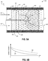
- FIG. 5B shows example sample condition in the mixing region of the device in FIG. 5A .
- the inner surface of the sample inspection device may be pretreated to facilitate sample entry into the chamber.
- the inner surface may be pretreated during manufacturing the sample inspection device.
- the inner surface may alternatively or additionally be pretreated before loading the samples into the device.
- FIGS. 2A-2C, 3A-3C, 4 and 5A show example configurations of the sample inspection device with relative positioning of the various components. These figures are not drawn to scale. If shown directly contacting each other, or directly coupled, then such elements may be referred to as directly contacting or directly coupled, respectively. Similarly, elements shown contiguous or adjacent to one another may be contiguous or adjacent to each other, respectively. As another example, elements positioned apart from each other with only a space there-between and no other components may be referred to as such, in at least one example.
- topmost element or point of element in the z axis may be referred to as a "top” of the component and a bottommost element or point of the element in the z axis may be referred to as a "bottom” of the component, in at least one example.
- top/bottom, upper/lower, above/below may be relative to the z-axis and used to describe positioning of elements of the figures relative to one another.
- FIG. 6 shows an example method for manufacturing the sample inspection device.
- FIG. 7 illustrates the procedures for manufacturing the sample inspection device according to the method of FIG. 6 .
- the sample inspection device may be made from two silicon wafers each deposited with a layer of electron transparent material. The two deposited wafers are bonded together by a patterned layer. The patterned layer forms the multiple pillars and the bonding layer.
- the sample inspection device with multiple disconnected chambers may be used individually for screening discrete sample conditions, as shown in FIG. 8 .
- the sample inspection device with multiple connected chambers may be used for screening continuously varied sample conditions, as shown in FIG. 9 .
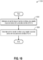
- the sample inspection device with connected chambers can be used together with the sample inspection device with disconnected chambers for fast identifying the optimal sample condition, as shown in FIG. 10 .
- the optimal range of sample condition may be first identified using the device with connected chamber.
- the optimal sample condition within the optimal range may then be identified using the device with disconnected chamber.
- the cryo-EM system may include a transmission electron microscopy (TEM) system 100 for imaging vitrified samples.
- the TEM system 100 includes an electron source 10 that emits charged particles along emission axis 110, such as electron beam 11, towards a column 12.
- the electron source 10 may generate high energy electrons, that is, electrons having typical energies of between about 10 keV and 1,000 keV.
- the column 12 may include one or more condenser lens, such as condenser lenses 120 and 121, and one or more aperture, such as aperture 122.
- Column 12 collimates electrons generated from electron source 10 and directs the electron beam onto sample inspection device 14.
- the sample inspection device 14 may be held by a sample holder 13.
- the sample inspection device may be any of the sample inspection devices described herein.
- the sample holder 13 may adjust sample position by tilting and/or translating the sample.
- the sample holder may be kept at temperatures well below zero degrees for cryogenic imaging.
- a condenser aperture 15 may be optionally inserted into the beam path to allow the electron beam to irradiate only a selected area of the sample.
- the TEM system 100 may be used for acquiring both diffraction patterns and EM images of the sample.
- the scattered electrons may transmit through the sample inspection device 14 and be collected by detector 25 after travelling sequentially through objective lens 123, intermediate lens 126, and projector lens 127, as shown with the solid lines.
- the un-scattered beam may be blocked by beam stopper 17.
- the collected scattered electrons be used to form an electron diffraction pattern, such as a selected area electron diffraction (SAED) pattern.
- SAED selected area electron diffraction
- the beam stopper 17 is removed from the beam path.
- the electrons transmitted from the sample inspection device 14 travel sequentially through object lens 123, intermediate lens 126 and projector lens 127, and form a TEM image of the sample on detector 25, as shown with the dashed lines.
- the detector 25 may detect the received electrons and send the signal to image processor 24 to form an image.
- the detector 25 may include an amplifier for amplifying the signal before sending the signal to the image processor 24.
- the detector 25 may be a CCD camera or a CMOS camera.
- different detectors may be used for detecting signals generated by the interaction of the electrons with the sample.
- the detector may detect x-rays and/or photons.
- the controller 30 may control the operation of the TEM system 100, either manually in response to operator instructions or automatically in accordance with computer readable instructions stored in non-transitory memory (or computer readable medium) 32 of the controller 30.
- the controller 30 may include a processor 24 and be configured to execute the computer readable instructions stored in the memory 32 and control various components of the TEM system 100 in order to implement any of the methods described herein. For example, the controller may adjust the imaging mode to acquire the diffraction pattern or the EM image by adjusting the position of the selected area aperture 15 and the objective diaphragm 124.
- the controller 30 may adjust the dose of the electron beam irradiated towards the sample by adjusting current density.
- the current density may be adjusted by adjusting the condenser optics (such as condenser lens 120 and 121).
- the controller 30 may adjust the profile of the incident beam by adjusting one or more apertures and/or lens in column 12.
- the controller 30 may adjust the sample position and/or orientation relative to the incident beam by adjusting the sample holder 13.
- the controller 30 may be configured to automatically acquiring images at one location or multiple locations of the sample inspection device 14.
- the controller 30 may further be coupled to a display 31 to display notifications and/or images of the sample.
- the controller 30 may receive user inputs from user input device 33.
- the user input device 33 may include keyboard, mouse, or touchscreen.
- the diffraction pattern and the EM images may be acquired with other microscopy systems.
- the diffraction patterns may be acquired by optical based microscopy systems.
- the diffraction pattern may be X-ray diffraction pattern acquired from an X-ray diffraction system.
- the EM image may be acquired from a scanning transmission electron microscopy (STEM) system.
- STEM scanning transmission electron microscopy
- FIGS. 2A-2C show an example of the sample inspection device 200 with a single chamber.
- An inlet and an outlet are fluidically connected with the chamber.
- the sample may flow into the chamber via the inlet and be inspected through a window covering at least a portion of the chamber.
- FIG. 2A is a top view of the sample inspection device 200.
- the sample inspection device 200 maybe rectangular.
- the sample inspection device may be 10 x 3.3 mm 2 .
- Window 201, inlet 203, and outlet 204 are formed in the top layer 211 of the sample inspection device.
- the window 201, inlet 203, and outlet 204 may be formed by creating tapered recesses 202, 205, and 206, respectively, in the top layer 211.
- the opening of the recesses (202, 205, and 206) in the x-y plane decreases as the opening approaching the chamber 231.
- the recesses (202, 205, and 206) have a depth the same as the thickness of the top layer 211.
- the recesses (202, 205, and 206) are created by etching a silicon wafer.
- the thickness of the top layer 211 may be 300 um.
- the minimal dimension of window 201 in the x-y plane may be larger than 100 um.
- a large window area provides a large area with uniform thickness and heat capacity, which may facilitate building high quality ice during vitrification.
- window 201 is square with a perimeter greater than 100 um.
- window 201 is square with a perimeter around 200 um.
- window 201 may be other shapes such as rectangular or round.
- the inlet 203 and outlet 204 are square with a perimeter between 80-180 um. In other examples, inlet 203 and outlet 204 may be of other shapes, such as rectangular or round.
- the window 201 covers at least a portion of chamber 231.
- the inlet 203 and the outlet 204 are in fluid communication with chamber 231.
- a sample may flow into chamber 231 from inlet 203 via channel 209, and flow from chamber 231 to the outlet 204 via channel 210.
- the sample within the chamber may be inspected via window 201.
- FIG. 2B is a cross-section view of the sample inspection device 200 in the x-z plane along A-A' of FIG. 2A .
- Two electron transparent layers 217 and 218 are positioned between top layer 211 and bottom layer 215.
- the top electron transparent layer 217 is in direct contact with the top layer 211
- the bottom electron transparent layer 218 is in direct contact with bottom layer 215.
- the top electron transparent layer 217 and the bottom electron transparent layer 218 are bonded by a bonding layer 232 and one or more pillars 212.
- the thickness of the electron transparent layers 217 and 218 may be 20 nm.
- a tapered recess 242 is formed in the bottom layer 215 and aligned with recess 202 so that charged particles, such as electrons, may transmit through the sample inspection device through window 201. Similar to recess 202, the opening of recess 242 in the x-y plane decreases as the opening approaching the chamber 231.
- the height of recess 242 is the same as the thickness 252 of the bottom layer 215.
- the thickness 251 of the top layer 211 may be the same as the thickness 252 of the bottom layer 215.
- Window 201 includes a portion of at least one of the two electron transparent layers 217 and 218.
- the portion of the electron transparent layer 217 forming window 202 is of a continuously material.
- Chamber 231 is formed between the electron transparent layers 217 and 218.
- the distance between the two electron transparent layers (or the height of the chamber) may be 50-100 nm.
- Multiple pillars 212 are arranged between the two electron transparent layers 217 and 218, allowing sample flowing around the pillar.
- Each of pillar 212 extends from the top electron transparent layer 217 to the bottom electron transparent layer 218.
- Each of pillar 212 has one end bonded to the top electron transparent layer 217 and the other end bonded to the bottom electron transparent layer 218.
- the sample inspection device may retain the shape during the process of sample loading, sample vitrification, and sample imaging.
- the shape of the pillars in the x-y cross-section may be round, oval, or rectangular.
- Window 201 covers at least one of the pillars 212.
- the cross-section area of each pillar in the x-y plane may be 3 um 2 - 350 um 2 .
- the pillars (212, 213) and the bonding layer 232 may be manufactured in the same process step and out of the same material. Charged particles may transmit through the window 201 between the gaps of the pillars 212, so that the sample surrounding the pillars may be imaged.
- window 201 has at least a region allowing the charged particles to transmit through and at least a region where the charged particles are blocked by the pillar.
- the area of the window may be increased. Increased window area allows larger imaging area and reduces stage traveling distance while inspecting the sample with the charged particle imaging system. Further, large window area facilitates homogeneous sample cooling during vitrification.
- the pillars provide mechanical support of the window and increase robustness of the sample inspection device.
- Channels 209 and 210 are formed in the bottom layer 215 to connect inlet 203 and outlet 204 with chamber 231, respectively.
- the channels may be created by etching into the bottom layer 215.
- the height 255 of channels 209 and 210 may be 0.1-10 um.
- multiple pillars 213 may optionally arranged in the chamber, with one end bonded to the top electron transparent layer 217.
- the chamber 231 is evacuated.
- the inlet 203 and outlet 204 are hermetic sealed by a thin membrane.
- inlet 203 and outlet 204 are sealed by the top electron transparent layer 217, as shown in FIG. 2B .
- the sample inspection device only has inlet but no outlet.
- the inlet may be hermetic sealed with a thin membrane. The sample may flow into the chamber by poking and breaking the thin membrane.
- Buffering chambers 207 and 208 are arranged between inlet 203 and chamber 231, and between chamber 231 and outlet 204, respectively.
- the sample flows from the inlet to the region of the chamber 231 covered by window 201 via buffering chamber 207.
- the buffering chamber may be a part of chamber 231, as shown in FIG. 2B-2C .
- the buffering chambers 207 and 208 are between the two electron transparent layers 217 and 218. No pillar is arranged in the buffering chamber.
- the buffering chambers may be a part of channel 209 and 210.
- the pillar-free buffering chamber may avoid back-flow of the sample from chamber 231 towards inlet 203.
- FIG. 2C is a cross-section view of the sample inspection device 200 in the x-y plane along B-B' of FIG. 2B .
- Part of chamber 231 is covered by window 201.
- the edge of the window is delineated by dashed line 230.
- Buffering chambers 207 and 208 fluidically connect the chamber region covered by the window with the inlet 203 and outlet 204, respectively.
- the window 201 covers multiple pillars 212. In other words, the window 201 is supported by multiple pillars 212.
- the sample may flow sequentially from the inlet 203 to the region of chamber 231 covered by window 201 via channel 209 and buffering chamber 207. If the sample inspection device includes an outlet 204, the sample may be drained from the region of chamber 231 covered by window 201 to the outlet via buffering chamber 208 and channel 210.
- the sample inspection device may be round.
- the sample inspection device may be round with a diameter of 3 mm
- FIGS. 3A-3C show an example of the sample inspection device 300 with two disconnected chambers. Each chamber has an inlet fluidically connected with the chamber. In this example, the sample inspection device 300 does not include outlet. Samples in both chambers may be inspected via a window. In some examples, one or more of the chambers may be connected to one or more outlet.
- FIG. 3A is a top view of the sample inspection device 300.
- Window 301, the first inlet 303, and the second inlet 304 are formed by creating tapered recesses 302, 305, and 306 in the top layer 311, respectively.
- Window 301 covers both a portion of the first chamber 331 and a portion of the second chamber 332.
- the first chamber 331 and second chamber 332 are not fluidically connected.
- the first chamber 331 and second chamber 332 are separated by wall 360.
- the first inlet 303 is fluidically connected with the first chamber 331 by channel 309.
- the second inlet 304 is fluidically connected with the second chamber 332 by channel 310.
- the thickness of the top layer 311 may be 300 um.
- the minimal dimension of window 301 in the x-y plane may be greater than 100 um.
- window 301 is square with a perimeter larger than 100 um.
- window 301 is square with a perimeter around 200 um.
- window 301 may be of other shapes such as rectangular or round.
- inlet 303 and inlet 304 are square with a perimeter between 80-180 um. In other examples, inlet 303 and inlet 304 may be of other shapes, such as rectangular or round.
- FIG. 3B is a cross-section view of the sample inspection device 300 in the x-z plane along C-C' of FIG. 3A .
- Two electron transparent layers 317 and 318 are positioned between top layer 311 and bottom layer 315.
- the top electron transparent layer 317 is in direct contact with the top layer 311, and the bottom electron transparent layer 318 is in direct contact with bottom layer 315.
- the top electron transparent layer 317 and the bottom electron transparent layer 318 are bonded by the bonding layer 311 and pillars 312.
- the pillars (312, 313, and 373) and the bonding layer 311 may be manufactured in the same process step and out of the same material.
- the thickness of the electron transparent layers 317 and 318 may be 20 nm.
- the openings of the tapered recesses 305, 302, and 306 decreases and the opening approaching the top electron transparent layer 317.
- the depths of the tapered recesses are the same as the thickness 351 of the top layer 311.
- a tapered recess 342 is formed in the bottom layer 315 and aligned with recess 302 so that charged particles, such as electrons, may transmit through the sample inspection device through window 301.
- the opening of recess 342 in the x-y plane decreases as the opening approaching the bottom electron transparent layer 318.
- the height of recess 342 is the same as the thickness 352 of the bottom layer 315.
- the thickness 351 of the top layer 211 may be the same as the thickness 352 of the bottom layer 315.
- Channels 309 and 310 are formed in the bottom layer 315 to connect the first inlet 303 with the first chamber 331, and to connect the second inlet 304 with the second chamber 332, respectively.
- the channels may be created by etching into the bottom layer 315.
- the height 355 of channel 309 and the height 356 of channel 310 may be 0.1-10 um. Pillars 313 and 373 may optionally be positioned in the channel 309 and/or channel 310.
- the pillars 313 and 373 may bond to the top electron transparent layer 317.
- the first inlet 303 and the second inlet 304 are hermetic sealed by a thin membrane from the first chamber 331 and the second chamber 332, respectively.
- the thin membrane is formed by the top electron transparent layer 317, as shown in FIG. 3B .
- the first chamber 331 and the second chamber 332 may be evacuated. The liquid sample may flow into the chamber by poking or breaking the thin membrane.
- FIG. 3C is a cross-section view of the sample inspection device 300 in the x-y plane along D-D' of FIG. 3B .
- Window 301 covers both a portion of the first chamber 331 and a portion of the second chamber 332. The edge of the window is delineated by dashed line 330.
- Buffering chamber 307 fluidically connects the region of the first chamber covered by the window 301 with the inlet 303.
- Buffering chamber 308 fluidically connects the region of the second chamber covered by the window 301 with the inlet 304.
- the window 301 covers multiple pillars 312. In other words, the window 301 is supported by multiple pillars 312.
- a first sample may flow sequentially from the first inlet 303 to the region of chamber 331 covered by window 301 via channel 309 and buffering chamber 307.
- a second sample may flow sequentially from the second inlet 304 to the region of chamber 332 covered by window 301 via channel 310 and buffering chamber 308.
- FIG. 4 is a cross-section view of a part of a sample inspection device 400 with four disconnected chambers 451, 452, 453 and 454 formed between two electron transparent layers bonded by bonding layer 402.
- a window 401 covers at least a portion of each chamber.
- the edge 470 of the window is delineated with dashed line.
- the region covered by window 401 in the x-y plane is indicated by diagonal lines within the window edge 470.
- Window 401 includes at least a portion of a continuous top electron transparent layer.
- the minimal dimension of window 401 in the x-y plane may be greater than 100 um.
- the sample inspection device may not have outlet, and the inlets are sealed by a thin film, similar to the sample inspection device of FIGS. 3A-3C . Four different samples may be transferred to different chambers of the sample inspection device and imaged through the window 401.
- the first chamber 411 and the third chamber 431 are separated from the second chamber 421 and the fourth chamber 441 by wall 403.
- the first chamber 411 and the second chamber 421 are separated from the third chamber 431 and the fourth chamber 441 by wall 404.
- Each chamber may include a region arranged with multiple pillars and a region without pillars.
- the region without pillars is also referred herein as buffering chamber.
- the first chamber 411 includes a region arranged with multiple pillars 412 and pillar-free buffering chamber 410.
- the second chamber 421 includes a region arranged with multiple pillars 422 and pillar-free buffering chamber 420.
- the third chamber 431 includes a region arranged with multiple pillars 432 and pillar-free buffering chamber 430.
- the fourth chamber 441 includes a region arranged with multiple pillars 442 and pillar-free buffering chamber 440.
- Window 401 covers at least one pillar in each of the chambers. In other words, the entirety of at least one pillar in the x-y plane is covered by window 401 in the x-y plane.
- the pillars are shown in stadium shape in the x-y plane.
- the cross-section of the pillar may be in other shapes, such as rectangle or round. In some embodiments, the pillars may be in different shapes in one sample inspection device.
- Each of the chambers is in fluidical connection with a different inlet (not shown) via a channel (451, 452, 453, or 454).
- Multiple pillars (461, 462, 463, and 464) may optionally be arranged within the channel.
- the buffering chamber may be included in the channel instead of the chamber.
- the number of chambers of the sample inspection device may be any integer number, such as 16, 32, or 64.
- FIG. 5A is a cross-sectional view of a part of an example sample inspection device 500.
- the sample inspection device 500 includes connected chambers formed between two electron transparent layers bonded by bonding layer 502.
- the first chamber 521 and the second chamber 522 receive the first sample and the second sample from different inlets (not shown), as indicated by arrow 551 and 522, respectively.
- the first chamber 521 and the second chamber 522 are fluidically separated upstream (that is, a direction opposite to x-axis arrow direction) of the device by wall 506 and are fluidically connected downstream of the device.
- the first sample and the second sample are mixed downstream (that is, arrow direction of x-axis) in mixing region 591 of the sample inspection device.
- the flow direction of portions of the first sample and the second sample are as indicated by arrows 553 and 554, respectively.
- the first sample, the second sample, and the mixture of the samples may be inspected through a window formed by at least a portion of the two electron transparent layers.
- the window covers region 501 in the x-y plane.
- the region 501 is covered by a continuous portion of an electron transparent layer (such as the top electron transparent layer).
- Dashed line 510 delineates the edge of the window covered region 501.
- the window covered region 501 includes the mixing region 591, where the samples are mixed.
- the window may also cover a part of wall 506.
- the window covered region 501 includes at least one pillar of multiple pillars 511 arranged between the two electron transparent layers.
- the pillars 511 are round in the x-y plane.
- the cross-section of pillars 511 may be other shapes, such as stadium or rectangular.
- Each chamber (521 and 522) of the sample inspection device 500 may include a pillar-free buffering chamber (531 and 532) upstream of the region of window covered region 501.
- the sample inspection device may include more than two connected chambers for mixing more than two samples.
- the window may cover the region where the samples are mixed.
- the first sample and the second sample may be transferred to the sample inspection device simultaneously. From the moment of transferring the samples to the sample inspection device, a laminar, stationary flow may be established for each sample. Sample mixing occurs at the interface of these two parallel flows in the mixing region. Gradient of sample conditions may form in the mixing region.
- the sample condition is a function of the sample position in the mixing region. In another example, the sample condition may be a function of the sample position as well as a waiting period from transferring the sample to the time of vitrification. Different sample conditions, such as sample ratios, may be observed at different locations of the mixing region at different time point. The spatial distribution of the sample ratio in the mixing region 591 changes over time.
- FIG. 5B shows the ratio between sample 2 and sample 1 along line 590 across the mixing region 591 of FIG. 5A .
- the sample ratio 581 does not change with time.
- the sample ratio 581 decreases as the distance in the x-axis from the end of wall 506 increases.
- the sample ratio 581 changes with time. For example, at time T2, later than time T1, the sample ratio 582 increases from sample ratio 581 at T1.
- the sample inspection devices shown in FIGS. 2A-2C, 3A-3C, 4 and 5A include one or more chambers covered by a single window.
- the single window includes a part of a continuous electron transparent layer.
- the window covers and is supported by at least one pillar bonded between the two electron transparent layers.
- the pillar may have a cross-section of a single shape or multiple shapes.
- all or a portion of the inner surface (that is, surface in direct contact with the sample during sample loading and imaging) of the sample inspection device may be pretreated to facilitate sample loading. The pretreatment may be done at room temperature.
- the surface pretreatment can be done via different experimental approaches.
- the surface may be pretreated by surface activation method at room temperature.
- the inner surface of the sample inspection device may be treated with chemical solutions to enable proper surface wetting, facilitate sample entry into the device, and facilitate adhesion of the sample into chamber.
- the surface of the sample inspection device may be treated by incubating the solution on the surface or flowing the solution through the surface.
- a buffer with optimum concentration of detergent or a hydrophilic anti-fouling compound, such as PEG that doesn't interfere with structure and functionality of target protein may be flown through the sample inspection device before transferring or loading the sample into the device to modify the inner surface of the device.
- the chemicals may covalently bind to the inner surface of the device.
- the inner surface of the sample inspection device may be treated by plasma cleaning.
- charged air is applied in high voltage via radical reaction to increase the hydrophilicity of the surface.
- the inner surface of the sample inspection device may be pretreated by irradiating the inner surface with radiation, such ultraviolet light irradiation (UV).
- UV ultraviolet light irradiation
- the inner surface is exposed to UV light to alter the surface tension and surface free energy which increase the wettability of surface.
- FIG. 6 is an example method 600 for manufacturing the sample inspection device.
- FIG. 7 illustrates the procedures of method 600 for manufacturing the sample inspection device in FIGS. 2A-2C .
- the diameter of each wafer in the x-y plane may be 4 inches.
- the thickness of the wafers may be 300 um.
- a layer of silicon nitride is deposited on one surface of each wafer.
- the thickness of the silicon nitride layer may be 20 nm.
- the silicon nitride layer is deposited by low-pressure chemical vapor deposition (LPCVD).
- Plot 701 of FIG. 7 shows a x-z cross-section of the first wafer 711 deposited with the electron transparent silicon nitride layer 712.
- a patterned layer is deposited over the silicon nitride layer of the first wafer.
- the thickness of the patterned layer may be 50-100 nm.
- the patterned layer may be borophosphosilicate glass (BPSG).
- the patterned layer is deposited by plasma-enhanced vapor deposition (PECVD).
- Plot 702 of FIG. 7 shows the patterned layer 724 deposited over the silicon nitride layer 712.
- the patterned layer 724 may form one or more of the pillars 721 within in the chamber (such as chamber 231 of FIGS. 2A-2C ), pillars 722 in the channel (such as channel 209 of FIGS. 2A-2C ), and bonding layer (such as bonding layer 232 of FIGS. 2A-2C ).
- channels are etched in the second wafer.
- the channels may be formed by etching through the silicon nitride layer deposited on the second wafer.
- the depth of the channel may be 0.1-10 um.
- Plot 703 shows channels 733 etched into second wafer 731 deposited with silicon nitride layer 732.
- the depth 735 of the channels 733 may be 0.1-10 um.
- the first wafer from step 606 and the second wafer from step 608 may be aligned and bonded in vacuum or low-pressure of inert gas by direct or fusion bonding.
- Plot 704 shows the processed first wafer of plot 702 and the processed second wafer of plot 703 aligned and bonded together.
- the bonded wafer is etched.
- the bonded wafer may be etched to expose the silicon nitride layer.
- Plot 705 of FIG. 7 shows recesses 751, 752, 753 and 754 being etched to the bonded wafer to expose the silicon nitride layer 712 and 732.
- one or more of the window, the inlet, and the outlet may be formed on the bonded wafer.
- the etched wafer may be diced into multiple individual devices.
- the inner surface of the sample inspection device may be pretreated.
- the inner surface of the sample inspection device may be pretreated before aligning and bonding the wafers at step 610.
- the inner surface may be irradiated with radiation, plasma cleaning, or heating.
- the inner surface may be pretreated by immersing a part or all of the inner surface of the device sequentially in one or more chemical solutions.
- the inner surface may be pretreated by sequentially flowing the solutions over the inner surface.
- the solutions may be a buffer with optimum concentration of detergent or anti-fouling chemicals such as PEG.
- the inner surface of the sample inspection device may be pretreated by heating the device after etching the bounded wafer at step 612.
- the inner surface may be pretreated by flowing the solutions through the device after aligning and bonding the wafers at step 610.
- FIG. 8 shows method 800 for screening sample condition of multiple samples using the sample inspection device with disconnected chambers, such as the sample inspection devices of FIGS. 3A-3C and FIG. 4 .
- Samples with different sample conditions may be transferred to different chambers of the sample inspection device and imaged.
- the optimal sample condition may be selected based on the cryo-EM images of the samples.
- a purified protein solution may be mixed with multiple buffer solutions to obtain samples with different sample conditions.
- the samples may have different protein-to-buffer ratios, different protein concentrations, or different buffer concentrations.
- the sample inspection device may optionally be pretreated before transferring or loading the samples into the device.
- the sample inspection device may be pretreated by plasma cleaning or flowing solutions through the device.
- a buffer with optimum concentration of detergent or anti-fouling chemicals such as PEG may be flown through the inspection device sequentially before transferring the sample into the device to modify the inner surface.
- the inlet and/or outlet of the sample inspection device is sealed. The seal is first broken before pretreating the sample inspection device.
- each sample of the prepared samples is transferred to one chamber of the sample inspection device.
- the samples may be transferred to the sample inspection device simultaneously or sequentially. For example, a small amount of a sample may be placed in the recess of the inlet of the sample inspection device. Then, the thin film sealing the inlet is poked and broken so that the small amount of the sample may flow in and fill the portion of the chamber covered by the window.
- the samples transferred to the sample inspection device are vitrified.
- the sample inspection device loaded with the multiple samples may be vitrified by plunge freezing.
- sample images are acquired from each chamber of the sample inspection device, for example, using the cryo-EM imaging system of FIG. 1 .
- a charged particle beam may be directed to a location on the window, and towards the sample surrounding one of the pillars covered by the window.
- the image of the sample may be formed based on charged particles transmitted through the sample inspection device.
- Multiple images of a sample at different locations of the chamber may be taken, wherein the sample at different locations has the same sample condition.
- the optimal sample condition that provides the best sample quality may be determined based on the sample images acquired from each chamber.
- the sample quality of each sample may be evaluated based on the images of each sample acquired at 808.
- the optimal sample condition corresponds to the best sample quality may be identified and used for sample preparation in the single particle analysis.
- samples with different sample conditions may be vitrified, and imaged in a single device. Discrete sample conditions may be evaluated.
- multiple samples with a variety of constructs may be loaded into multiple chambers of the one sample inspection device to determine the optimal stabilization method for the protein.
- different protein complexes of a target protein with a variety of ligand or compounds may be loaded and inspected using one sample inspection device.
- different proteins or multiple versions of a protein complex in different states (such as open/close or rotary) may be loaded and inspected using one sample inspection device.
- FIG. 9 shows method 900 for screening sample condition of multiple samples using the sample inspection device with connected chambers, such as the sample inspection device of FIG. 5 .
- the samples are transferred to the sample inspection device and mixed in the device. Images may be taken at different locations of a mixing region covered by the window of the sample inspection device. The optimal range of sample condition may be determined based on the images and the corresponding imaging location.
- a first sample is a purified protein solution
- the second sample is a buffer
- the sample inspection device may optionally be pretreated before transferring or loading samples into the device.
- the sample inspection device may be treated by plasma cleaning or flowing solutions through the device.
- a buffer with optimum concentration of detergent or anti-fouling chemicals such as PEG may be flown sequentially through the inspection device before transferring the sample into the device to modify the inner surface.
- the samples are mixed in the sample inspection device with connected chambers.
- Mixing the sample includes transferring the sample to the sample inspection device by flowing each sample into one inlet of the device. For example, a small amount of a sample may be placed in the recess of the inlet of the sample inspection device. Then, the thin film sealing the inlet is broken so that the small amount of the sample may flow into the region of chamber covered by the window. The samples may be flown into the device simultaneously, and mixed downstream of the device in the mixing region covered by the window.
- the sample within the sample inspection device is vitrified after a waiting period from flowing the samples into the sample inspection device.
- the waiting period may be predetermined.
- the spatial distribution of sample condition in the mixing region may change with the waiting time.
- the sample in the sample inspection device may be vitrified by plunge freezing.
- sample images are acquired from multiple locations in the mixing region of the sample inspection device, for example using the cryo-EM imaging system of FIG. 1 .
- Each location in the mixing region may have a different sample condition.
- the images may be taken at predetermined locations.
- the sample quality of the acquired sample images is evaluated, and locations where the images have good sample qualities may be identified.
- the optimal range of sample condition is determined. Determining the optimal range of sample condition may include determining the sample conditions at the identified locations from 910. In some examples, the sensitivity of a sample condition may be determined by identifying the differences among multiple locations based on images from 908. Based on the sample conditions at the identified locations, an optimal range of sample condition may be determined.
- the sample condition at each of the identified locations may be determined experimentally.
- the mixed sample at each identified location may be extracted and analyzed to obtain the sample condition.
- the mixed sample may be extracted by breakout the sample inspection device using a focused ion-beam system.
- the sample condition may be determined based on the identified locations and a calibrated sample condition distribution.
- the calibrated sample condition distribution may be generated theoretically via simulation based on parameters including one or more of the properties of the samples, the waiting time, temperature, and flow rate of the sample when transferring the sample to the sample inspection device.
- the calibrated sample condition distribution may be generated experimentally by measuring the sample condition of calibration samples in the sample inspection device.
- the samples may be mixed, vitrified, and imaged in a single device.
- a continuous range of sample conditions of mixed samples may be obtained and evaluated.
- FIG. 10 shows method 1000 for screening sample condition using both the sample inspection device with connected chamber and the sample inspection device with dis-connected chamber.
- the optimal range of sample condition may be first determined by screening a large variation of sample conditions using the sample inspection device with connected chamber. Then, multiple samples with sample conditions within the optimal range may be screened individually to determine optimum sample condition using the sample inspection device with disconnected chamber.
- the optimal range of the sample condition is determined using method 900 of FIG. 9 .
- a protein solution and one or more buffers may be transferred to the sample inspection device with connected chambers.
- sample conditions that may result in the optimal sample quality are determined.
- buffer screening using method 900 provides a global search of the optimal range.
- the sample condition within each sample image may vary.
- limited number of the mixed sample at a particular sample condition can be imaged.
- method 900 may provide an optimal range of sample condition that includes the optimum sample condition, but not specific optimum sample condition.
- samples with sample conditions within the optimal range determined at 1002 are prepared.
- the samples may be screened using method 800 of FIG. 8 to determine the optimum sample condition within the optimal range.
- Multiple images of the sample with a particular sample condition may be obtained, wherein each image may be taken at a different location of the chamber. As such, the sample quality may be accurately and reliably evaluated.
- each of the step 1002 and 1004 may be repeated for screening different buffers and/or accurately identifying the optimum sample condition.
- a global sample condition screening is first performed using the sample inspection device with connected chambers to identify the optimal range.
- a localized sample condition screening is performed within the optimal range to identify the optimum condition.
- the multiscale screening strategy may significantly reduce the sample condition screening time and facilitate locating the global optimum sample condition for single particle analysis.
- the technical effect of providing a window covering at least one pillar of multiple pillars for sample inspection is to provide mechanical strength of the window covered area of the sample inspection device.
- the technical effect of bonding the pillar to the two electron transparent layers is to prevent bulging during sample loading and vitrification.
- the technical effect of imaging multiple samples within a chamber is that sample qualities may be better controlled for vitrification and the imaging.
- the technical effect of mixing multiple samples in the sample inspection device is that a continuous distribution of sample condition may be obtained.
- the technical effect of controlling the waiting time between flowing the sample into the sample inspection device and the sample vitrification is that the distribution of sample condition in the mixing region may be adjusted.
- a sample inspection device includes a first chamber formed between a top electron transparent layer and a bottom electron transparent layer for holding a first sample; multiple pillars within the first chamber, each pillar of the multiple pillars extends from the top electron transparent layer to the bottom electron transparent layer; and a window formed with a portion of at least one of the top electron transparent layer and the bottom electron transparent layer for inspecting the first sample in the first chamber, the window covering at least one of the multiple pillars.
- the window allows inspecting the first sample surrounding the at least one of the multiple pillars covered by the window.
- a second example of the method optionally includes the first example and further includes a second chamber formed between the top electron transparent layer and the bottom electron transparent layer for holding a second sample, and wherein the window covers a portion of the second chamber for inspecting the second sample in the second chamber.
- a third example of the method optionally includes one or more of the first to the second examples, and further includes wherein the multiple pillars are arranged between the top electron transparent layer and the bottom electron transparent layer in the second chamber.
- a fourth example of the method optionally includes one or more of the first to the third examples, and further includes wherein the first chamber and the second chamber are fluidically connected in a region covered by the window.
- a fifth example of the method optionally includes one or more of the first to the fourth examples, and further includes wherein one end of each pillar of the multiple pillars is bonded to the top electron transparent layer and the other end of the pillar is bonded to the bottom electron transparent layer.
- a sixth example of the method optionally includes one or more of the first to the fifth examples, and further includes an inlet and a buffering chamber, wherein the inlet is fluidically connected to the first chamber via the buffering chamber, and no pillar is arranged in the buffering chamber.
- a seventh example of the method optionally includes one or more of the first to the sixth examples, and further includes wherein at least a portion of the top electron transparent layer and/or the bottom electron transparent layer in contact with the first sample is pretreated to facilitate transferring the first sample into the first chamber.
- An eighth example of the method optionally includes one or more of the first to the seventh examples, and further includes wherein a region of the window not covering the at least one of the multiple pillars allows a charged particle beam transmitting through the sample inspection device.
- a ninth example of the method optionally includes one or more of the first to the eighth examples, and further includes wherein a distance between the two electron transparent layers is less than 100 nm.
- a method of inspecting a sample using a sample inspection device includes flowing a first sample into a first chamber of the sample inspection device, wherein the first chamber is formed between a top electron transparent layer and a bottom electron transparent layer, multiple pillars are arranged with in the first chamber, and each pillar of the multiple pillars extends from the top electron transparent layer to the bottom electron transparent layer; directing a charged particle beam towards a window of the sample inspection device, wherein the window is formed with a portion of at least one of the top electron transparent layer and the bottom electron transparent layer, and the window covers at least one of the multiple pillars; and forming a first image of the first sample based on charged particles transmitted through the sample inspection device.
- the method further includes treating an inner surface of the inspection device before flowing the first sample into the first chamber.
- a second example of the method optionally includes the first example and further includes wherein directing the charged particle beam towards the window includes directing the beam to a location of the window not covering the at least one of the multiple pillars.
- a third example of the method optionally includes one or more of the first to the second examples, and further includes vitrifying the first sample in the sample inspection device after flowing the first sample into the first chamber and before directing the charged particle beam towards the window of the sample inspection device.
- a fourth example of the method optionally includes one or more of the first to the third examples, and further includes wherein directing the charged particle beam towards the window of the sample inspection device and forming the first image of the first sample based on the charged particles transmitted through the sample inspection device includes: directing the charged particle beam at a first location of the first chamber, and forming the first image of the first sample based on the charged particles transmitted through the sample inspection device.
- a fifth example of the method optionally includes one or more of the first to the fourth examples, and further includes flowing a second sample into a second chamber of the sample inspection device, the second chamber formed between the top electron transparent layer and the bottom electron transparent layer, the second chamber fluidically separated from the first chamber, the window covering at least a portion of the second chamber; directing the charged particle beam towards a second location in the second chamber; and forming a second image of the second sample based on charged particles transmitted through the sample inspection device.
- a sixth example of the method optionally includes one or more of the first to the fifth examples, and further includes wherein the first sample and the second sample have different sample conditions, and the method further comprising determining an optimal sample condition by comparing the first image and the second image.
- a seventh example of the method optionally includes one or more of the first to the sixth examples, and further includes while flowing the first sample into the first chamber, flowing a second sample into a second chamber formed between the top electron transparent layer and the bottom electron transparent layer, and mixing the first sample and the second sample in a mixing region of the sample inspection device covered by the window; and wherein directing the charged particle beam towards the window includes directing the charged particle beam at multiple locations within the mixing region, wherein ratios between the first sample and the second sample at the multiple locations are different.
- An eighth example of the method optionally includes one or more of the first to the seventh examples, and further includes wherein forming the image based on charged particles transmitted through the sample inspection device includes forming an image of each of the multiple locations based on charged the particles transmitted through the sample inspection device; and the method further comprising comparing the multiple images to determine an optimal sample condition.
- a ninth example of the method optionally includes one or more of the first to the eighth examples, and further includes vitrifying the first sample, the second sample, and the mixture of the first sample and the second sample in the sample inspection device before directing the charged particle beam towards the window; and determining the ratios between the first sample and the second sample at the multiple locations based on a duration between flowing the first sample and the second sample into the sample inspection device and the vitrification.
Landscapes
- Chemical & Material Sciences (AREA)
- Analytical Chemistry (AREA)
- General Health & Medical Sciences (AREA)
- Life Sciences & Earth Sciences (AREA)
- Health & Medical Sciences (AREA)
- Biochemistry (AREA)
- Physics & Mathematics (AREA)
- General Physics & Mathematics (AREA)
- Immunology (AREA)
- Pathology (AREA)
- Crystallography & Structural Chemistry (AREA)
- Analysing Materials By The Use Of Radiation (AREA)
- Sampling And Sample Adjustment (AREA)
Abstract
Description
- The present description relates generally to methods and devices for preparing samples for single particle analysis, and more particularly, to optimizing the sample quality for single particle analysis based on cryogenic electron microscopy imaging.
- Single particle analysis based on cryogenic electron microscopy (cryo-EM) images may solve structures of biological macromolecules at near atomic resolution. Sample preparation is a key step for obtaining high quality cryo-EM images of the macromolecules. As an example, in order to solve protein structure, the protein sample is prepared by mixing the protein with one or more buffer solutions. The sample construct, as well as buffer conditions including PH level, salt concentration, surfactant concentration, and detergent concentration, need to be optimized to solubilize and stabilize the protein for the optimal cryo-EM result. However, preparing and imaging vitrified protein samples with different sample conditions requires extensive trial and error testing, and can become extremely time consuming.
- In one embodiment, a sample inspection device is used for screening the sample condition. The sample inspection device comprises one or more chambers formed between a top electron transparent layer and a bottom electron transparent layer for holding a first sample; multiple pillars within the first chamber, each pillar of the multiple pillars extends from the top electron transparent layer to the bottom electron transparent layer; and a window formed with a portion of at least one of the top electron transparent layer and the bottom electron transparent layer for inspecting the first sample in the first chamber, the window covering at least one of the multiple pillars. In this way, samples with multiple sample conditions may be vitrified and imaged within the same sample inspection device.
- In another embodiment, a method for inspecting a sample using a sample inspection device comprises flowing a first sample into a first chamber of the sample inspection device, wherein the first chamber is formed between a top electron transparent layer and a bottom electron transparent layer, multiple pillars are arranged within the first chamber, and each pillar of the multiple pillars extends from the top electron transparent layer to the bottom electron transparent layer; directing a charged particle beam towards a window of the sample inspection device, wherein the window is formed with a portion of at least one of the top electron transparent layer and the bottom electron transparent layer, and the window covers at least one of the multiple pillars; and forming a first image of the first sample based on charged particles transmitted through the sample inspection device.
- It should be understood that the summary above is provided to introduce in simplified form a selection of concepts that are further described in the detailed description. It is not meant to identify key or essential features of the claimed subject matter, the scope of which is defined uniquely by the claims that follow the detailed description. Furthermore, the claimed subject matter is not limited to implementations that solve any disadvantages noted above or in any part of this disclosure.
-
-
FIG. 1 illustrates a cryogenic electron microscopy system. -
FIGS. 2A, 2B, and 2C show an example sample inspection device with one chamber. -
FIGS. 3A, 3B, and 3C show an example sample inspection device with two disconnected chambers. -
FIG. 4 shows an example sample inspection device with four disconnected chambers. -
FIG. 5A shows an example sample inspection device with two connected chambers. -
FIG. 5B shows varied sample condition distribution in the sample inspection device ofFIG. 5A . -
FIG. 6 is a method for manufacturing the sample inspection device. -
FIG. 7 illustrates procedures for manufacturing the sample inspection device, according to the method ofFIG. 6 . -
FIG. 8 shows an example method for screening sample condition using a sample inspection device with disconnected chambers. -
FIG. 9 shows an example method for screening sample condition using a sample inspection device with connected chamber. -
FIG. 10 shows an example method for screening sample condition using both a sample inspection device with disconnected chambers and a sample inspection device with connected chamber. - Like reference numerals refer to corresponding parts throughout the several views of the drawings.
- The following description relates to systems and methods for screening samples for cryogenic electron microscopy (cryo-EM) based single particle analysis. The cryo-EM imaging may be performed using an imaging system shown in
FIG. 1 . - In order to perform single particle analysis, the sample is undergone multiple sample preparation steps to achieve an optimal sample condition before being imaged with the cryo-EM imaging system. The sample condition may include buffer type and PH level, salt and detergent type and concentration, as well as surfactant concentration. The sample condition may also include nanodisc size, lipid to protein ratio, and critical micelle concentration.
- The sample preparation steps may include purifying the sample, mixing the purified sample with buffers, and vitrifying the mixture. One of the sample preparation steps is mixing the sample, such as a protein, with one or more buffers to solubilize and stabilize the sample. For example, the protein maybe stabilized by adding constructs such as nanodisc, cross-linker, and or scaffolds. By mixing the sample with the one or more buffers, the buffer system of the sample is exchanged from the buffer system used during the purification process and/or sample storage to a buffer system suitable for cryo-EM imaging.
- The sample quality for single particle analysis may be determined based on the cryo-EM images of the sample. The sample quality may include the particle quality, the sample-grid quality, and the cryo-EM image quality. The particle quality may include one or more of the tertiary and quaternary structure, aggregation state, stability, particle binding, particle size, and particle similarity. The sample-grid quality may include one or more of ice formation, and particle distribution and particle orientation on the grid. The image quality may include one or more of contrast and resolution.
- Though multiple techniques are available for screening the sample for protein expression and purification without cryo-EM imaging, the sample quality for single particle analysis can only be accurately and reliably determined based on the cryo-EM image of the vitrified sample. As a result, the sample condition can only be accurately and reliably evaluated based on the cryo-EM images. Because it is difficult to predict the sample condition for a new sample based on known optimal sample conditions for other samples, multiple iterations of sample preparation and cryo-EM imaging have to be performed to search for the optimal sample condition for the new sample.
- In order to address this issue, various examples of the sample inspection device and methods for screening the sample condition using the sample inspection device are presented for accelerating the search for the optimal sample condition. The sample inspection device may have one chamber (
FIGS. 2A-2C ), multiple fluidically disconnected chambers (FIGS. 3A-3C andFIG. 4 ), or multiple fluidically connected chambers (FIG. 5A ) formed between a top electron transparent layer and a bottom electron transparent layer. The samples with different sample conditions may be loaded into the one or more chambers and inspected by imaging through a window form by at least a portion of the electron transparent layers. Multiple pillars are arranged in the chamber. The window covers at least one of the pillars. Each pillar has one end bonded with the top electron transparent layer and the other end bonded with the bottom electron transparent layer. The sample may flow around the pillar. The pillars provide mechanical strength and robustness to the window. More importantly, by bonding the pillar with the electron transparent layers, bulging during sample loading and device vitrification may be prevented. - For the sample inspection device with disconnected chambers, discrete sample conditions may be imaged and analyzed. For the sample inspection device with fluidically connected chambers, a gradient of sample conditions may be formed in the mixing region, and continuous varied sample conditions may be imaged and analyzed.
FIG. 5B shows example sample condition in the mixing region of the device inFIG. 5A . By providing a window covering multiple samples or samples with different sample conditions, multiple locations of the sample and/or multiple samples may be imaged with minimal translation of the imaging beam or the sample. Further, a large window area provides a large area with uniform thickness and heat capacity, which may facilitate building high quality ice during vitrification. - The inner surface of the sample inspection device may be pretreated to facilitate sample entry into the chamber. The inner surface may be pretreated during manufacturing the sample inspection device. The inner surface may alternatively or additionally be pretreated before loading the samples into the device.
-
FIGS. 2A-2C, 3A-3C, 4 and 5A show example configurations of the sample inspection device with relative positioning of the various components. These figures are not drawn to scale. If shown directly contacting each other, or directly coupled, then such elements may be referred to as directly contacting or directly coupled, respectively. Similarly, elements shown contiguous or adjacent to one another may be contiguous or adjacent to each other, respectively. As another example, elements positioned apart from each other with only a space there-between and no other components may be referred to as such, in at least one example. Further, as shown in the figures, a topmost element or point of element in the z axis may be referred to as a "top" of the component and a bottommost element or point of the element in the z axis may be referred to as a "bottom" of the component, in at least one example. As used herein, top/bottom, upper/lower, above/below, may be relative to the z-axis and used to describe positioning of elements of the figures relative to one another. -
FIG. 6 shows an example method for manufacturing the sample inspection device.FIG. 7 illustrates the procedures for manufacturing the sample inspection device according to the method ofFIG. 6 . The sample inspection device may be made from two silicon wafers each deposited with a layer of electron transparent material. The two deposited wafers are bonded together by a patterned layer. The patterned layer forms the multiple pillars and the bonding layer. - The sample inspection device with multiple disconnected chambers may be used individually for screening discrete sample conditions, as shown in
FIG. 8 . The sample inspection device with multiple connected chambers may be used for screening continuously varied sample conditions, as shown inFIG. 9 . The sample inspection device with connected chambers can be used together with the sample inspection device with disconnected chambers for fast identifying the optimal sample condition, as shown inFIG. 10 . The optimal range of sample condition may be first identified using the device with connected chamber. The optimal sample condition within the optimal range may then be identified using the device with disconnected chamber. - Turning to
FIG. 1 , a cryo-EM imaging system in accordance with an embodiment of the disclosure is shown. The cryo-EM system may include a transmission electron microscopy (TEM)system 100 for imaging vitrified samples. TheTEM system 100 includes anelectron source 10 that emits charged particles alongemission axis 110, such aselectron beam 11, towards acolumn 12. Theelectron source 10 may generate high energy electrons, that is, electrons having typical energies of between about 10 keV and 1,000 keV. In some embodiments, thecolumn 12 may include one or more condenser lens, such ascondenser lenses aperture 122.Column 12 collimates electrons generated fromelectron source 10 and directs the electron beam ontosample inspection device 14. Thesample inspection device 14 may be held by asample holder 13. The sample inspection device may be any of the sample inspection devices described herein. Thesample holder 13 may adjust sample position by tilting and/or translating the sample. The sample holder may be kept at temperatures well below zero degrees for cryogenic imaging. Acondenser aperture 15 may be optionally inserted into the beam path to allow the electron beam to irradiate only a selected area of the sample. - The
TEM system 100 may be used for acquiring both diffraction patterns and EM images of the sample. In the diffraction imaging mode, the scattered electrons may transmit through thesample inspection device 14 and be collected bydetector 25 after travelling sequentially throughobjective lens 123,intermediate lens 126, andprojector lens 127, as shown with the solid lines. The un-scattered beam may be blocked bybeam stopper 17. The collected scattered electrons be used to form an electron diffraction pattern, such as a selected area electron diffraction (SAED) pattern. In the EM imaging mode, thebeam stopper 17 is removed from the beam path. The electrons transmitted from thesample inspection device 14 travel sequentially throughobject lens 123,intermediate lens 126 andprojector lens 127, and form a TEM image of the sample ondetector 25, as shown with the dashed lines. - The
detector 25 may detect the received electrons and send the signal to imageprocessor 24 to form an image. Thedetector 25 may include an amplifier for amplifying the signal before sending the signal to theimage processor 24. In one example, thedetector 25 may be a CCD camera or a CMOS camera. In some embodiments, different detectors may be used for detecting signals generated by the interaction of the electrons with the sample. For example, the detector may detect x-rays and/or photons. - The
controller 30 may control the operation of theTEM system 100, either manually in response to operator instructions or automatically in accordance with computer readable instructions stored in non-transitory memory (or computer readable medium) 32 of thecontroller 30. Thecontroller 30 may include aprocessor 24 and be configured to execute the computer readable instructions stored in thememory 32 and control various components of theTEM system 100 in order to implement any of the methods described herein. For example, the controller may adjust the imaging mode to acquire the diffraction pattern or the EM image by adjusting the position of the selectedarea aperture 15 and the objective diaphragm 124. Thecontroller 30 may adjust the dose of the electron beam irradiated towards the sample by adjusting current density. For example, the current density may be adjusted by adjusting the condenser optics (such ascondenser lens 120 and 121). Thecontroller 30 may adjust the profile of the incident beam by adjusting one or more apertures and/or lens incolumn 12. Thecontroller 30 may adjust the sample position and/or orientation relative to the incident beam by adjusting thesample holder 13. Thecontroller 30 may be configured to automatically acquiring images at one location or multiple locations of thesample inspection device 14. Thecontroller 30 may further be coupled to adisplay 31 to display notifications and/or images of the sample. Thecontroller 30 may receive user inputs fromuser input device 33. Theuser input device 33 may include keyboard, mouse, or touchscreen. - Though the TEM system is described by way of example, it should be understood that the diffraction pattern and the EM images may be acquired with other microscopy systems. As one example, the diffraction patterns may be acquired by optical based microscopy systems. As one example, the diffraction pattern may be X-ray diffraction pattern acquired from an X-ray diffraction system. As another example, the EM image may be acquired from a scanning transmission electron microscopy (STEM) system. The present discussion of TEM system is provided merely as an example of one suitable imaging modality.
-
FIGS. 2A-2C show an example of thesample inspection device 200 with a single chamber. An inlet and an outlet are fluidically connected with the chamber. The sample may flow into the chamber via the inlet and be inspected through a window covering at least a portion of the chamber. -
FIG. 2A is a top view of thesample inspection device 200. Thesample inspection device 200 maybe rectangular. For example, the sample inspection device may be 10 x 3.3 mm2.Window 201,inlet 203, andoutlet 204 are formed in thetop layer 211 of the sample inspection device. Thewindow 201,inlet 203, andoutlet 204 may be formed by creatingtapered recesses top layer 211. The opening of the recesses (202, 205, and 206) in the x-y plane decreases as the opening approaching thechamber 231. The recesses (202, 205, and 206) have a depth the same as the thickness of thetop layer 211. In one example, the recesses (202, 205, and 206) are created by etching a silicon wafer. The thickness of thetop layer 211 may be 300 um. The minimal dimension ofwindow 201 in the x-y plane may be larger than 100 um. A large window area provides a large area with uniform thickness and heat capacity, which may facilitate building high quality ice during vitrification. In one example,window 201 is square with a perimeter greater than 100 um. In another example,window 201 is square with a perimeter around 200 um. In other examples,window 201 may be other shapes such as rectangular or round. In one example, theinlet 203 andoutlet 204 are square with a perimeter between 80-180 um. In other examples,inlet 203 andoutlet 204 may be of other shapes, such as rectangular or round. Thewindow 201 covers at least a portion ofchamber 231. Theinlet 203 and theoutlet 204 are in fluid communication withchamber 231. A sample may flow intochamber 231 frominlet 203 viachannel 209, and flow fromchamber 231 to theoutlet 204 viachannel 210. The sample within the chamber may be inspected viawindow 201. -
FIG. 2B is a cross-section view of thesample inspection device 200 in the x-z plane along A-A' ofFIG. 2A . Two electrontransparent layers top layer 211 andbottom layer 215. The top electrontransparent layer 217 is in direct contact with thetop layer 211, and the bottom electrontransparent layer 218 is in direct contact withbottom layer 215. The top electrontransparent layer 217 and the bottom electrontransparent layer 218 are bonded by abonding layer 232 and one ormore pillars 212. The thickness of the electrontransparent layers tapered recess 242 is formed in thebottom layer 215 and aligned withrecess 202 so that charged particles, such as electrons, may transmit through the sample inspection device throughwindow 201. Similar to recess 202, the opening ofrecess 242 in the x-y plane decreases as the opening approaching thechamber 231. The height ofrecess 242 is the same as thethickness 252 of thebottom layer 215. Thethickness 251 of thetop layer 211 may be the same as thethickness 252 of thebottom layer 215. -
Window 201 includes a portion of at least one of the two electrontransparent layers transparent layer 217 formingwindow 202 is of a continuously material.Chamber 231 is formed between the electrontransparent layers Multiple pillars 212 are arranged between the two electrontransparent layers pillar 212 extends from the top electrontransparent layer 217 to the bottom electrontransparent layer 218. Each ofpillar 212 has one end bonded to the top electrontransparent layer 217 and the other end bonded to the bottom electrontransparent layer 218. By bonding each end of the pillar to one of the two electron transparent layers, the sample inspection device may retain the shape during the process of sample loading, sample vitrification, and sample imaging. In one example, the shape of the pillars in the x-y cross-section may be round, oval, or rectangular.Window 201 covers at least one of thepillars 212. The cross-section area of each pillar in the x-y plane may be 3 um2 - 350 um2. The pillars (212, 213) and thebonding layer 232 may be manufactured in the same process step and out of the same material. Charged particles may transmit through thewindow 201 between the gaps of thepillars 212, so that the sample surrounding the pillars may be imaged. In other words,window 201 has at least a region allowing the charged particles to transmit through and at least a region where the charged particles are blocked by the pillar. By arranging pillars within the chamber covered by the window, the area of the window may be increased. Increased window area allows larger imaging area and reduces stage traveling distance while inspecting the sample with the charged particle imaging system. Further, large window area facilitates homogeneous sample cooling during vitrification. Moreover, the pillars provide mechanical support of the window and increase robustness of the sample inspection device. -
Channels bottom layer 215 to connectinlet 203 andoutlet 204 withchamber 231, respectively. The channels may be created by etching into thebottom layer 215. The height 255 ofchannels multiple pillars 213 may optionally arranged in the chamber, with one end bonded to the top electrontransparent layer 217. In one embodiment, thechamber 231 is evacuated. Theinlet 203 andoutlet 204 are hermetic sealed by a thin membrane. In one example,inlet 203 andoutlet 204 are sealed by the top electrontransparent layer 217, as shown inFIG. 2B . In another embodiment, the sample inspection device only has inlet but no outlet. The inlet may be hermetic sealed with a thin membrane. The sample may flow into the chamber by poking and breaking the thin membrane. - Buffering
chambers inlet 203 andchamber 231, and betweenchamber 231 andoutlet 204, respectively. The sample flows from the inlet to the region of thechamber 231 covered bywindow 201 viabuffering chamber 207. In some embodiments, the buffering chamber may be a part ofchamber 231, as shown inFIG. 2B-2C . The bufferingchambers transparent layers channel chamber 231 towardsinlet 203. -
FIG. 2C is a cross-section view of thesample inspection device 200 in the x-y plane along B-B' ofFIG. 2B . Part ofchamber 231 is covered bywindow 201. The edge of the window is delineated by dashedline 230. Bufferingchambers inlet 203 andoutlet 204, respectively. Thewindow 201 coversmultiple pillars 212. In other words, thewindow 201 is supported bymultiple pillars 212. The sample may flow sequentially from theinlet 203 to the region ofchamber 231 covered bywindow 201 viachannel 209 andbuffering chamber 207. If the sample inspection device includes anoutlet 204, the sample may be drained from the region ofchamber 231 covered bywindow 201 to the outlet viabuffering chamber 208 andchannel 210. - In some embodiments, the sample inspection device may be round. For example, the sample inspection device may be round with a diameter of 3 mm
-
FIGS. 3A-3C show an example of thesample inspection device 300 with two disconnected chambers. Each chamber has an inlet fluidically connected with the chamber. In this example, thesample inspection device 300 does not include outlet. Samples in both chambers may be inspected via a window. In some examples, one or more of the chambers may be connected to one or more outlet. -
FIG. 3A is a top view of thesample inspection device 300.Window 301, thefirst inlet 303, and thesecond inlet 304 are formed by creatingtapered recesses top layer 311, respectively.Window 301 covers both a portion of thefirst chamber 331 and a portion of thesecond chamber 332. Thefirst chamber 331 andsecond chamber 332 are not fluidically connected. Within the region covered bywindow 301, thefirst chamber 331 andsecond chamber 332 are separated bywall 360. Thefirst inlet 303 is fluidically connected with thefirst chamber 331 bychannel 309. Thesecond inlet 304 is fluidically connected with thesecond chamber 332 bychannel 310. - The thickness of the
top layer 311 may be 300 um. The minimal dimension ofwindow 301 in the x-y plane may be greater than 100 um. In one example,window 301 is square with a perimeter larger than 100 um. In another example,window 301 is square with a perimeter around 200 um. In other examples,window 301 may be of other shapes such as rectangular or round. In one example,inlet 303 andinlet 304 are square with a perimeter between 80-180 um. In other examples,inlet 303 andinlet 304 may be of other shapes, such as rectangular or round. -
FIG. 3B is a cross-section view of thesample inspection device 300 in the x-z plane along C-C' ofFIG. 3A . Two electrontransparent layers top layer 311 andbottom layer 315. The top electrontransparent layer 317 is in direct contact with thetop layer 311, and the bottom electrontransparent layer 318 is in direct contact withbottom layer 315. The top electrontransparent layer 317 and the bottom electrontransparent layer 318 are bonded by thebonding layer 311 andpillars 312. The pillars (312, 313, and 373) and thebonding layer 311 may be manufactured in the same process step and out of the same material. The thickness of the electrontransparent layers recesses transparent layer 317. The depths of the tapered recesses are the same as thethickness 351 of thetop layer 311. - A
tapered recess 342 is formed in thebottom layer 315 and aligned withrecess 302 so that charged particles, such as electrons, may transmit through the sample inspection device throughwindow 301. The opening ofrecess 342 in the x-y plane decreases as the opening approaching the bottom electrontransparent layer 318. The height ofrecess 342 is the same as thethickness 352 of thebottom layer 315. Thethickness 351 of thetop layer 211 may be the same as thethickness 352 of thebottom layer 315. -
Channels bottom layer 315 to connect thefirst inlet 303 with thefirst chamber 331, and to connect thesecond inlet 304 with thesecond chamber 332, respectively. The channels may be created by etching into thebottom layer 315. The height 355 ofchannel 309 and the height 356 ofchannel 310 may be 0.1-10 um.Pillars channel 309 and/orchannel 310. Thepillars transparent layer 317. In some embodiments, thefirst inlet 303 and thesecond inlet 304 are hermetic sealed by a thin membrane from thefirst chamber 331 and thesecond chamber 332, respectively. In one example, the thin membrane is formed by the top electrontransparent layer 317, as shown inFIG. 3B . Thefirst chamber 331 and thesecond chamber 332 may be evacuated. The liquid sample may flow into the chamber by poking or breaking the thin membrane. -
FIG. 3C is a cross-section view of thesample inspection device 300 in the x-y plane along D-D' ofFIG. 3B .Window 301 covers both a portion of thefirst chamber 331 and a portion of thesecond chamber 332. The edge of the window is delineated by dashedline 330.Buffering chamber 307 fluidically connects the region of the first chamber covered by thewindow 301 with theinlet 303.Buffering chamber 308 fluidically connects the region of the second chamber covered by thewindow 301 with theinlet 304. Thewindow 301 coversmultiple pillars 312. In other words, thewindow 301 is supported bymultiple pillars 312. A first sample may flow sequentially from thefirst inlet 303 to the region ofchamber 331 covered bywindow 301 viachannel 309 andbuffering chamber 307. A second sample may flow sequentially from thesecond inlet 304 to the region ofchamber 332 covered bywindow 301 viachannel 310 andbuffering chamber 308. -
FIG. 4 is a cross-section view of a part of asample inspection device 400 with fourdisconnected chambers bonding layer 402. Awindow 401 covers at least a portion of each chamber. Theedge 470 of the window is delineated with dashed line. The region covered bywindow 401 in the x-y plane is indicated by diagonal lines within thewindow edge 470.Window 401 includes at least a portion of a continuous top electron transparent layer. The minimal dimension ofwindow 401 in the x-y plane may be greater than 100 um. The sample inspection device may not have outlet, and the inlets are sealed by a thin film, similar to the sample inspection device ofFIGS. 3A-3C . Four different samples may be transferred to different chambers of the sample inspection device and imaged through thewindow 401. - The first chamber 411 and the
third chamber 431 are separated from thesecond chamber 421 and thefourth chamber 441 bywall 403. The first chamber 411 and thesecond chamber 421 are separated from thethird chamber 431 and thefourth chamber 441 bywall 404. Each chamber may include a region arranged with multiple pillars and a region without pillars. The region without pillars is also referred herein as buffering chamber. For example, the first chamber 411 includes a region arranged withmultiple pillars 412 and pillar-free buffering chamber 410. Thesecond chamber 421 includes a region arranged withmultiple pillars 422 and pillar-free buffering chamber 420. Thethird chamber 431 includes a region arranged withmultiple pillars 432 and pillar-free buffering chamber 430. Thefourth chamber 441 includes a region arranged withmultiple pillars 442 and pillar-free buffering chamber 440.Window 401 covers at least one pillar in each of the chambers. In other words, the entirety of at least one pillar in the x-y plane is covered bywindow 401 in the x-y plane. Herein, the pillars are shown in stadium shape in the x-y plane. The cross-section of the pillar may be in other shapes, such as rectangle or round. In some embodiments, the pillars may be in different shapes in one sample inspection device. - Each of the chambers is in fluidical connection with a different inlet (not shown) via a channel (451, 452, 453, or 454). Multiple pillars (461, 462, 463, and 464) may optionally be arranged within the channel.
- In one embodiment, the buffering chamber may be included in the channel instead of the chamber. In some embodiment, the number of chambers of the sample inspection device may be any integer number, such as 16, 32, or 64.
-
FIG. 5A is a cross-sectional view of a part of an examplesample inspection device 500. Thesample inspection device 500 includes connected chambers formed between two electron transparent layers bonded bybonding layer 502. Thefirst chamber 521 and thesecond chamber 522 receive the first sample and the second sample from different inlets (not shown), as indicated byarrow first chamber 521 and thesecond chamber 522 are fluidically separated upstream (that is, a direction opposite to x-axis arrow direction) of the device bywall 506 and are fluidically connected downstream of the device. The first sample and the second sample are mixed downstream (that is, arrow direction of x-axis) in mixingregion 591 of the sample inspection device. The flow direction of portions of the first sample and the second sample are as indicated byarrows - The first sample, the second sample, and the mixture of the samples may be inspected through a window formed by at least a portion of the two electron transparent layers. The window covers
region 501 in the x-y plane. Theregion 501 is covered by a continuous portion of an electron transparent layer (such as the top electron transparent layer). Dashedline 510 delineates the edge of the window coveredregion 501. The window coveredregion 501 includes the mixingregion 591, where the samples are mixed. The window may also cover a part ofwall 506. The window coveredregion 501 includes at least one pillar ofmultiple pillars 511 arranged between the two electron transparent layers. Herein, thepillars 511 are round in the x-y plane. In other examples, the cross-section ofpillars 511 may be other shapes, such as stadium or rectangular. - Each chamber (521 and 522) of the
sample inspection device 500 may include a pillar-free buffering chamber (531 and 532) upstream of the region of window coveredregion 501. In some embodiments, the sample inspection device may include more than two connected chambers for mixing more than two samples. The window may cover the region where the samples are mixed. - The first sample and the second sample may be transferred to the sample inspection device simultaneously. From the moment of transferring the samples to the sample inspection device, a laminar, stationary flow may be established for each sample. Sample mixing occurs at the interface of these two parallel flows in the mixing region. Gradient of sample conditions may form in the mixing region. In one example, if the stationary sample flow remains from transferring the sample to the sample inspection device to the time of vitrification, the sample condition is a function of the sample position in the mixing region. In another example, the sample condition may be a function of the sample position as well as a waiting period from transferring the sample to the time of vitrification. Different sample conditions, such as sample ratios, may be observed at different locations of the mixing region at different time point. The spatial distribution of the sample ratio in the mixing
region 591 changes over time. -
FIG. 5B shows the ratio betweensample 2 andsample 1 alongline 590 across the mixingregion 591 ofFIG. 5A . In one example, if both samples maintain laminar and stationary flow from transferring the samples to the sample inspection device to the time of vitrification, thesample ratio 581 does not change with time. Thesample ratio 581 decreases as the distance in the x-axis from the end ofwall 506 increases. In another example, after transferring samples into the sample inspection device at T1, thesample ratio 581 changes with time. For example, at time T2, later than time T1, thesample ratio 582 increases fromsample ratio 581 at T1. - The sample inspection devices shown in
FIGS. 2A-2C, 3A-3C, 4 and 5A include one or more chambers covered by a single window. The single window includes a part of a continuous electron transparent layer. The window covers and is supported by at least one pillar bonded between the two electron transparent layers. The pillar may have a cross-section of a single shape or multiple shapes. In some examples, all or a portion of the inner surface (that is, surface in direct contact with the sample during sample loading and imaging) of the sample inspection device may be pretreated to facilitate sample loading. The pretreatment may be done at room temperature. - The surface pretreatment can be done via different experimental approaches. In one example, the surface may be pretreated by surface activation method at room temperature. The inner surface of the sample inspection device may be treated with chemical solutions to enable proper surface wetting, facilitate sample entry into the device, and facilitate adhesion of the sample into chamber. The surface of the sample inspection device may be treated by incubating the solution on the surface or flowing the solution through the surface. For example, a buffer with optimum concentration of detergent or a hydrophilic anti-fouling compound, such as PEG that doesn't interfere with structure and functionality of target protein, may be flown through the sample inspection device before transferring or loading the sample into the device to modify the inner surface of the device. In some examples, the chemicals may covalently bind to the inner surface of the device.
- In another example, the inner surface of the sample inspection device may be treated by plasma cleaning. For example, charged air is applied in high voltage via radical reaction to increase the hydrophilicity of the surface.
- In yet another example, the inner surface of the sample inspection device may be pretreated by irradiating the inner surface with radiation, such ultraviolet light irradiation (UV). The inner surface is exposed to UV light to alter the surface tension and surface free energy which increase the wettability of surface.
-
FIG. 6 is anexample method 600 for manufacturing the sample inspection device.FIG. 7 illustrates the procedures ofmethod 600 for manufacturing the sample inspection device inFIGS. 2A-2C . - At 602, two silicon wafers are prepared. In one example, the diameter of each wafer in the x-y plane may be 4 inches. The thickness of the wafers may be 300 um.
- At 604, a layer of silicon nitride is deposited on one surface of each wafer. The thickness of the silicon nitride layer may be 20 nm. In one example, the silicon nitride layer is deposited by low-pressure chemical vapor deposition (LPCVD). Plot 701 of
FIG. 7 shows a x-z cross-section of thefirst wafer 711 deposited with the electron transparentsilicon nitride layer 712. - At 606, a patterned layer is deposited over the silicon nitride layer of the first wafer. The thickness of the patterned layer may be 50-100 nm. The patterned layer may be borophosphosilicate glass (BPSG). In one example, the patterned layer is deposited by plasma-enhanced vapor deposition (PECVD). Plot 702 of
FIG. 7 shows the patternedlayer 724 deposited over thesilicon nitride layer 712. The patternedlayer 724 may form one or more of thepillars 721 within in the chamber (such aschamber 231 ofFIGS. 2A-2C ),pillars 722 in the channel (such aschannel 209 ofFIGS. 2A-2C ), and bonding layer (such asbonding layer 232 ofFIGS. 2A-2C ). - At 608, channels are etched in the second wafer. The channels may be formed by etching through the silicon nitride layer deposited on the second wafer. The depth of the channel may be 0.1-10 um. Plot 703 shows
channels 733 etched intosecond wafer 731 deposited withsilicon nitride layer 732. Thedepth 735 of thechannels 733 may be 0.1-10 um. - At 610, the first wafer from
step 606 and the second wafer fromstep 608 may be aligned and bonded in vacuum or low-pressure of inert gas by direct or fusion bonding. Plot 704 shows the processed first wafer ofplot 702 and the processed second wafer ofplot 703 aligned and bonded together. - At 612, the bonded wafer is etched. The bonded wafer may be etched to expose the silicon nitride layer. Plot 705 of
FIG. 7 showsrecesses silicon nitride layer - At 614, the etched wafer may be diced into multiple individual devices.
- The inner surface of the sample inspection device may be pretreated. In one example, the inner surface of the sample inspection device may be pretreated before aligning and bonding the wafers at
step 610. The inner surface may be irradiated with radiation, plasma cleaning, or heating. The inner surface may be pretreated by immersing a part or all of the inner surface of the device sequentially in one or more chemical solutions. The inner surface may be pretreated by sequentially flowing the solutions over the inner surface. The solutions may be a buffer with optimum concentration of detergent or anti-fouling chemicals such as PEG. In another example, the inner surface of the sample inspection device may be pretreated by heating the device after etching the bounded wafer atstep 612. In yet another example, the inner surface may be pretreated by flowing the solutions through the device after aligning and bonding the wafers atstep 610. -
FIG. 8 showsmethod 800 for screening sample condition of multiple samples using the sample inspection device with disconnected chambers, such as the sample inspection devices ofFIGS. 3A-3C andFIG. 4 . Samples with different sample conditions may be transferred to different chambers of the sample inspection device and imaged. The optimal sample condition may be selected based on the cryo-EM images of the samples. - At 802, multiple samples with different sample conditions are prepared. For example, a purified protein solution may be mixed with multiple buffer solutions to obtain samples with different sample conditions. The samples may have different protein-to-buffer ratios, different protein concentrations, or different buffer concentrations.
- At 803, the sample inspection device may optionally be pretreated before transferring or loading the samples into the device. The sample inspection device may be pretreated by plasma cleaning or flowing solutions through the device. For example, a buffer with optimum concentration of detergent or anti-fouling chemicals such as PEG may be flown through the inspection device sequentially before transferring the sample into the device to modify the inner surface. In some examples, if the inlet and/or outlet of the sample inspection device is sealed. The seal is first broken before pretreating the sample inspection device.
- At 804, each sample of the prepared samples is transferred to one chamber of the sample inspection device. The samples may be transferred to the sample inspection device simultaneously or sequentially. For example, a small amount of a sample may be placed in the recess of the inlet of the sample inspection device. Then, the thin film sealing the inlet is poked and broken so that the small amount of the sample may flow in and fill the portion of the chamber covered by the window.
- At 806, the samples transferred to the sample inspection device are vitrified. For example, the sample inspection device loaded with the multiple samples may be vitrified by plunge freezing.
- At 808, sample images are acquired from each chamber of the sample inspection device, for example, using the cryo-EM imaging system of
FIG. 1 . To image the sample in a chamber, a charged particle beam may be directed to a location on the window, and towards the sample surrounding one of the pillars covered by the window. The image of the sample may be formed based on charged particles transmitted through the sample inspection device. Multiple images of a sample at different locations of the chamber may be taken, wherein the sample at different locations has the same sample condition. - At 810, the optimal sample condition that provides the best sample quality may be determined based on the sample images acquired from each chamber. The sample quality of each sample may be evaluated based on the images of each sample acquired at 808. The optimal sample condition corresponds to the best sample quality may be identified and used for sample preparation in the single particle analysis.
- In this way, samples with different sample conditions may be vitrified, and imaged in a single device. Discrete sample conditions may be evaluated. In some examples, instead of loading the device chambers with one type of protein with different sample conditions, multiple samples with a variety of constructs may be loaded into multiple chambers of the one sample inspection device to determine the optimal stabilization method for the protein. In other examples, different protein complexes of a target protein with a variety of ligand or compounds may be loaded and inspected using one sample inspection device. In some examples, different proteins or multiple versions of a protein complex in different states (such as open/close or rotary) may be loaded and inspected using one sample inspection device.
-
FIG. 9 showsmethod 900 for screening sample condition of multiple samples using the sample inspection device with connected chambers, such as the sample inspection device ofFIG. 5 . The samples are transferred to the sample inspection device and mixed in the device. Images may be taken at different locations of a mixing region covered by the window of the sample inspection device. The optimal range of sample condition may be determined based on the images and the corresponding imaging location. - At 902, multiple samples are prepared. For example, a first sample is a purified protein solution, and the second sample is a buffer.
- At 903, the sample inspection device may optionally be pretreated before transferring or loading samples into the device. The sample inspection device may be treated by plasma cleaning or flowing solutions through the device. For example, a buffer with optimum concentration of detergent or anti-fouling chemicals such as PEG may be flown sequentially through the inspection device before transferring the sample into the device to modify the inner surface.
- At 904, the samples are mixed in the sample inspection device with connected chambers. Mixing the sample includes transferring the sample to the sample inspection device by flowing each sample into one inlet of the device. For example, a small amount of a sample may be placed in the recess of the inlet of the sample inspection device. Then, the thin film sealing the inlet is broken so that the small amount of the sample may flow into the region of chamber covered by the window. The samples may be flown into the device simultaneously, and mixed downstream of the device in the mixing region covered by the window.
- At 906, the sample within the sample inspection device is vitrified after a waiting period from flowing the samples into the sample inspection device. The waiting period may be predetermined. The spatial distribution of sample condition in the mixing region may change with the waiting time. The sample in the sample inspection device may be vitrified by plunge freezing.
- At 908, sample images are acquired from multiple locations in the mixing region of the sample inspection device, for example using the cryo-EM imaging system of
FIG. 1 . Each location in the mixing region may have a different sample condition. In one example, the images may be taken at predetermined locations. - At 910, the sample quality of the acquired sample images is evaluated, and locations where the images have good sample qualities may be identified.
- At 912, the optimal range of sample condition is determined. Determining the optimal range of sample condition may include determining the sample conditions at the identified locations from 910. In some examples, the sensitivity of a sample condition may be determined by identifying the differences among multiple locations based on images from 908. Based on the sample conditions at the identified locations, an optimal range of sample condition may be determined.
- In one example, at 914, the sample condition at each of the identified locations may be determined experimentally. The mixed sample at each identified location may be extracted and analyzed to obtain the sample condition. For example, the mixed sample may be extracted by breakout the sample inspection device using a focused ion-beam system.
- In another example, at 916, the sample condition may be determined based on the identified locations and a calibrated sample condition distribution. The calibrated sample condition distribution may be generated theoretically via simulation based on parameters including one or more of the properties of the samples, the waiting time, temperature, and flow rate of the sample when transferring the sample to the sample inspection device. Alternatively, the calibrated sample condition distribution may be generated experimentally by measuring the sample condition of calibration samples in the sample inspection device.
- In this way, the samples may be mixed, vitrified, and imaged in a single device. A continuous range of sample conditions of mixed samples may be obtained and evaluated.
-
FIG. 10 shows method 1000 for screening sample condition using both the sample inspection device with connected chamber and the sample inspection device with dis-connected chamber. The optimal range of sample condition may be first determined by screening a large variation of sample conditions using the sample inspection device with connected chamber. Then, multiple samples with sample conditions within the optimal range may be screened individually to determine optimum sample condition using the sample inspection device with disconnected chamber. - At 1002, the optimal range of the sample condition is determined using
method 900 ofFIG. 9 . For example, a protein solution and one or more buffers may be transferred to the sample inspection device with connected chambers. Based on the cryo-EM images, sample conditions that may result in the optimal sample quality are determined. Because a wide range of sample conditions may be obtained using the sample inspection device with connected chambers, bufferscreening using method 900 provides a global search of the optimal range. However, due to continuous variation in spatial distribution of sample conditions in the mixing region, the sample condition within each sample image may vary. Further, limited number of the mixed sample at a particular sample condition can be imaged. As such,method 900 may provide an optimal range of sample condition that includes the optimum sample condition, but not specific optimum sample condition. - At 1004, multiple samples with sample conditions within the optimal range determined at 1002 are prepared. The samples may be screened using
method 800 ofFIG. 8 to determine the optimum sample condition within the optimal range. Multiple images of the sample with a particular sample condition may be obtained, wherein each image may be taken at a different location of the chamber. As such, the sample quality may be accurately and reliably evaluated. - In some embodiments, each of the
step - In this way, a global sample condition screening is first performed using the sample inspection device with connected chambers to identify the optimal range. A localized sample condition screening is performed within the optimal range to identify the optimum condition. The multiscale screening strategy may significantly reduce the sample condition screening time and facilitate locating the global optimum sample condition for single particle analysis.
- The technical effect of providing a window covering at least one pillar of multiple pillars for sample inspection is to provide mechanical strength of the window covered area of the sample inspection device. The technical effect of bonding the pillar to the two electron transparent layers is to prevent bulging during sample loading and vitrification. The technical effect of imaging multiple samples within a chamber is that sample qualities may be better controlled for vitrification and the imaging. The technical effect of mixing multiple samples in the sample inspection device is that a continuous distribution of sample condition may be obtained. The technical effect of controlling the waiting time between flowing the sample into the sample inspection device and the sample vitrification is that the distribution of sample condition in the mixing region may be adjusted.
- In one embodiment, a sample inspection device includes a first chamber formed between a top electron transparent layer and a bottom electron transparent layer for holding a first sample; multiple pillars within the first chamber, each pillar of the multiple pillars extends from the top electron transparent layer to the bottom electron transparent layer; and a window formed with a portion of at least one of the top electron transparent layer and the bottom electron transparent layer for inspecting the first sample in the first chamber, the window covering at least one of the multiple pillars. In a first example of the device, the window allows inspecting the first sample surrounding the at least one of the multiple pillars covered by the window. A second example of the method optionally includes the first example and further includes a second chamber formed between the top electron transparent layer and the bottom electron transparent layer for holding a second sample, and wherein the window covers a portion of the second chamber for inspecting the second sample in the second chamber. A third example of the method optionally includes one or more of the first to the second examples, and further includes wherein the multiple pillars are arranged between the top electron transparent layer and the bottom electron transparent layer in the second chamber. A fourth example of the method optionally includes one or more of the first to the third examples, and further includes wherein the first chamber and the second chamber are fluidically connected in a region covered by the window. A fifth example of the method optionally includes one or more of the first to the fourth examples, and further includes wherein one end of each pillar of the multiple pillars is bonded to the top electron transparent layer and the other end of the pillar is bonded to the bottom electron transparent layer. A sixth example of the method optionally includes one or more of the first to the fifth examples, and further includes an inlet and a buffering chamber, wherein the inlet is fluidically connected to the first chamber via the buffering chamber, and no pillar is arranged in the buffering chamber. A seventh example of the method optionally includes one or more of the first to the sixth examples, and further includes wherein at least a portion of the top electron transparent layer and/or the bottom electron transparent layer in contact with the first sample is pretreated to facilitate transferring the first sample into the first chamber. An eighth example of the method optionally includes one or more of the first to the seventh examples, and further includes wherein a region of the window not covering the at least one of the multiple pillars allows a charged particle beam transmitting through the sample inspection device. A ninth example of the method optionally includes one or more of the first to the eighth examples, and further includes wherein a distance between the two electron transparent layers is less than 100 nm.
- In another embodiment, a method of inspecting a sample using a sample inspection device includes flowing a first sample into a first chamber of the sample inspection device, wherein the first chamber is formed between a top electron transparent layer and a bottom electron transparent layer, multiple pillars are arranged with in the first chamber, and each pillar of the multiple pillars extends from the top electron transparent layer to the bottom electron transparent layer; directing a charged particle beam towards a window of the sample inspection device, wherein the window is formed with a portion of at least one of the top electron transparent layer and the bottom electron transparent layer, and the window covers at least one of the multiple pillars; and forming a first image of the first sample based on charged particles transmitted through the sample inspection device. In a first example of the method, the method further includes treating an inner surface of the inspection device before flowing the first sample into the first chamber. A second example of the method optionally includes the first example and further includes wherein directing the charged particle beam towards the window includes directing the beam to a location of the window not covering the at least one of the multiple pillars. A third example of the method optionally includes one or more of the first to the second examples, and further includes vitrifying the first sample in the sample inspection device after flowing the first sample into the first chamber and before directing the charged particle beam towards the window of the sample inspection device. A fourth example of the method optionally includes one or more of the first to the third examples, and further includes wherein directing the charged particle beam towards the window of the sample inspection device and forming the first image of the first sample based on the charged particles transmitted through the sample inspection device includes: directing the charged particle beam at a first location of the first chamber, and forming the first image of the first sample based on the charged particles transmitted through the sample inspection device. A fifth example of the method optionally includes one or more of the first to the fourth examples, and further includes flowing a second sample into a second chamber of the sample inspection device, the second chamber formed between the top electron transparent layer and the bottom electron transparent layer, the second chamber fluidically separated from the first chamber, the window covering at least a portion of the second chamber; directing the charged particle beam towards a second location in the second chamber; and forming a second image of the second sample based on charged particles transmitted through the sample inspection device. A sixth example of the method optionally includes one or more of the first to the fifth examples, and further includes wherein the first sample and the second sample have different sample conditions, and the method further comprising determining an optimal sample condition by comparing the first image and the second image. A seventh example of the method optionally includes one or more of the first to the sixth examples, and further includes while flowing the first sample into the first chamber, flowing a second sample into a second chamber formed between the top electron transparent layer and the bottom electron transparent layer, and mixing the first sample and the second sample in a mixing region of the sample inspection device covered by the window; and wherein directing the charged particle beam towards the window includes directing the charged particle beam at multiple locations within the mixing region, wherein ratios between the first sample and the second sample at the multiple locations are different. An eighth example of the method optionally includes one or more of the first to the seventh examples, and further includes wherein forming the image based on charged particles transmitted through the sample inspection device includes forming an image of each of the multiple locations based on charged the particles transmitted through the sample inspection device; and the method further comprising comparing the multiple images to determine an optimal sample condition. A ninth example of the method optionally includes one or more of the first to the eighth examples, and further includes vitrifying the first sample, the second sample, and the mixture of the first sample and the second sample in the sample inspection device before directing the charged particle beam towards the window; and determining the ratios between the first sample and the second sample at the multiple locations based on a duration between flowing the first sample and the second sample into the sample inspection device and the vitrification.
Claims (15)
- A sample inspection device, comprising:a first chamber formed between a top electron transparent layer and a bottom electron transparent layer for holding a first sample;multiple pillars within the first chamber, each pillar of the multiple pillars extends from the top electron transparent layer to the bottom electron transparent layer; anda window formed with a portion of at least one of the top electron transparent layer and the bottom electron transparent layer for inspecting the first sample in the first chamber, the window covering at least one of the multiple pillars.
- The sample inspection device of claim 1, wherein the window allows inspecting the first sample surrounding the at least one of the multiple pillars covered by the window.
- The sample inspection device of any of claims 1 and 2, further comprising a second chamber formed between the top electron transparent layer and the bottom electron transparent layer for holding a second sample, and wherein the window covers a portion of the second chamber for inspecting the second sample in the second chamber.
- The sample inspection device of claim 3, wherein the multiple pillars are arranged between the top electron transparent layer and the bottom electron transparent layer in the second chamber.
- The sample inspection device of claim 3, wherein the first chamber and the second chamber are fluidically connected in a region covered by the window.
- The sample inspection device of claims 1-5, wherein at least a portion of the top electron transparent layer and/or the bottom electron transparent layer in contact with the first sample is pretreated to facilitate transferring the first sample into the first chamber
- A method of inspecting a sample using a sample inspection device, comprising:flowing a first sample into a first chamber of the sample inspection device, wherein the first chamber is formed between a top electron transparent layer and a bottom electron transparent layer, multiple pillars are arranged with in the first chamber, and each pillar of the multiple pillars extends from the top electron transparent layer to the bottom electron transparent layer;directing a charged particle beam towards a window of the sample inspection device, wherein the window is formed with a portion of at least one of the top electron transparent layer and the bottom electron transparent layer, and the window covers at least one of the multiple pillars; andforming a first image of the first sample based on charged particles transmitted through the sample inspection device.
- The method of claim 7, further comprising treating an inner surface of the inspection device before flowing the first sample into the first chamber.
- The method of any of claims 7 and 8, further comprising vitrifying the first sample in the sample inspection device after flowing the first sample into the first chamber and before directing the charged particle beam towards the window of the sample inspection device.
- The method of any of claims 7-9, wherein directing the charged particle beam towards the window of the sample inspection device and forming the first image of the first sample based on the charged particles transmitted through the sample inspection device includes:
directing the charged particle beam at a first location of the first chamber, and forming the first image of the first sample based on the charged particles transmitted through the sample inspection device. - The method of claim 10, further comprising:flowing a second sample into a second chamber of the sample inspection device, the second chamber formed between the top electron transparent layer and the bottom electron transparent layer, the second chamber fluidically separated from the first chamber, the window covering at least a portion of the second chamber;directing the charged particle beam towards a second location in the second chamber; andforming a second image of the second sample based on charged particles transmitted through the sample inspection device.
- The method of claim 11, wherein the first sample and the second sample have different sample conditions, and the method further comprising determining an optimal sample condition by comparing the first image and the second image.
- The method of claim 7, further comprising:
while flowing the first sample into the first chamber, flowing a second sample into a second chamber formed between the top electron transparent layer and the bottom electron transparent layer, and mixing the first sample and the second sample in a mixing region of the sample inspection device covered by the window; and wherein directing the charged particle beam towards the window includes directing the charged particle beam at multiple locations within the mixing region, wherein ratios between the first sample and the second sample at the multiple locations are different. - The method of claim 13, wherein forming the image based on charged particles transmitted through the sample inspection device includes forming an image of each of the multiple locations based on charged the particles transmitted through the sample inspection device; and the method further comprising comparing the multiple images to determine an optimal sample condition.
- The method of claim 14, further comprising vitrifying the first sample, the second sample, and the mixture of the first sample and the second sample in the sample inspection device before directing the charged particle beam towards the window; and determining the ratios between the first sample and the second sample at the multiple locations based on a duration between flowing the first sample and the second sample into the sample inspection device and the vitrification.
Priority Applications (1)
| Application Number | Priority Date | Filing Date | Title |
|---|---|---|---|
| EP22151911.9A EP4009347A3 (en) | 2019-09-09 | 2020-09-02 | Methods and devices for preparing sample for cryogenic electron microscopy |
Applications Claiming Priority (1)
| Application Number | Priority Date | Filing Date | Title |
|---|---|---|---|
| US16/565,058 US10921268B1 (en) | 2019-09-09 | 2019-09-09 | Methods and devices for preparing sample for cryogenic electron microscopy |
Related Child Applications (1)
| Application Number | Title | Priority Date | Filing Date |
|---|---|---|---|
| EP22151911.9A Division EP4009347A3 (en) | 2019-09-09 | 2020-09-02 | Methods and devices for preparing sample for cryogenic electron microscopy |
Publications (2)
| Publication Number | Publication Date |
|---|---|
| EP3790036A2 true EP3790036A2 (en) | 2021-03-10 |
| EP3790036A3 EP3790036A3 (en) | 2021-07-14 |
Family
ID=72340231
Family Applications (2)
| Application Number | Title | Priority Date | Filing Date |
|---|---|---|---|
| EP20194019.4A Pending EP3790036A3 (en) | 2019-09-09 | 2020-09-02 | Methods and devices for preparing sample for cryogenic electron microscopy |
| EP22151911.9A Pending EP4009347A3 (en) | 2019-09-09 | 2020-09-02 | Methods and devices for preparing sample for cryogenic electron microscopy |
Family Applications After (1)
| Application Number | Title | Priority Date | Filing Date |
|---|---|---|---|
| EP22151911.9A Pending EP4009347A3 (en) | 2019-09-09 | 2020-09-02 | Methods and devices for preparing sample for cryogenic electron microscopy |
Country Status (4)
| Country | Link |
|---|---|
| US (1) | US10921268B1 (en) |
| EP (2) | EP3790036A3 (en) |
| JP (1) | JP7596621B2 (en) |
| CN (1) | CN112557422B (en) |
Cited By (1)
| Publication number | Priority date | Publication date | Assignee | Title |
|---|---|---|---|---|
| WO2022257966A1 (en) * | 2021-06-08 | 2022-12-15 | The University Of Hong Kong | Application of metallo-supramolecular branched polymers in cryo-electron microscopy sample preparation |
Families Citing this family (6)
| Publication number | Priority date | Publication date | Assignee | Title |
|---|---|---|---|---|
| US10921268B1 (en) * | 2019-09-09 | 2021-02-16 | Fei Company | Methods and devices for preparing sample for cryogenic electron microscopy |
| EP3839489A1 (en) * | 2019-12-18 | 2021-06-23 | Universidad Rey Juan Carlos | Devices and methods for high angle liquid electron tomography |
| EP4141429B1 (en) * | 2021-08-24 | 2024-03-13 | Deutsches Elektronen-Synchrotron DESY | Sample cell, loading station, measuring device, method for inspecting and producing a flat crystal, use of a sample cell |
| US12553812B2 (en) * | 2021-09-13 | 2026-02-17 | Gregory Hirsch | Vacuum ultraviolet cryo-EM grid screening tool |
| US20260004597A1 (en) * | 2022-05-27 | 2026-01-01 | University Of Massachusetts | Methods and systems for imaging interactions between particles and fragments |
| CN117782742B (en) * | 2024-01-04 | 2026-07-17 | 北京大学 | Frozen solution sample preparation device suitable for ultrahigh vacuum system |
Family Cites Families (42)
| Publication number | Priority date | Publication date | Assignee | Title |
|---|---|---|---|---|
| US5672878A (en) * | 1996-10-24 | 1997-09-30 | Siemens Medical Systems Inc. | Ionization chamber having off-passageway measuring electrodes |
| US7241993B2 (en) * | 2000-06-27 | 2007-07-10 | Ebara Corporation | Inspection system by charged particle beam and method of manufacturing devices using the system |
| NL1027025C2 (en) * | 2004-09-13 | 2006-03-14 | Univ Delft Tech | Microreactor for a transmission electron microscope and heating element and method for manufacturing thereof. |
| JP2007294126A (en) * | 2006-04-21 | 2007-11-08 | Canon Inc | Electron emitting device, electron source, image display apparatus, and method for manufacturing electron emitting device |
| NL1032224C2 (en) * | 2006-07-21 | 2008-01-22 | Univ Delft Tech | Method for sample preparation for cryo-electron microscopy (CEM), microreactor and loading dock. |
| EP2009420A1 (en) * | 2007-06-29 | 2008-12-31 | FEI Company | Method for attaching a sample to a manipulator |
| JP5215701B2 (en) * | 2008-03-26 | 2013-06-19 | 日本電子株式会社 | Sample inspection apparatus and sample inspection method |
| US8059271B2 (en) * | 2009-02-04 | 2011-11-15 | The United States Of America As Represented By The Secretary Of The Army | Reusable sample holding device permitting ready loading of very small wet samples |
| EP2278306A1 (en) * | 2009-07-13 | 2011-01-26 | Fei Company | Method for inspecting a sample |
| EP2457078A4 (en) * | 2009-07-23 | 2014-07-30 | Insight Nanofluidics Inc | Nanofluidic cell |
| EP2316565A1 (en) * | 2009-10-26 | 2011-05-04 | Fei Company | A micro-reactor for observing particles in a fluid |
| WO2011100434A2 (en) * | 2010-02-10 | 2011-08-18 | Chistopher Su-Yan Own | Aberration-correcting dark-field electron microscopy |
| JP2011243483A (en) * | 2010-05-20 | 2011-12-01 | Jeol Ltd | Sample holder, inspection equipment, and inspection method |
| DK2601669T3 (en) * | 2010-08-02 | 2017-07-24 | Protochips Inc | ELECTRON MICROSCOPE SAMPLES TO CREATE A GAS OR LIQUID CELL WITH TWO SEMICONDUCTOR DEVICES |
| GB2484517B (en) * | 2010-10-14 | 2016-03-30 | Carl Zeiss Nts Ltd | Improvements in and relating to charged particle beam devices |
| US9207196B2 (en) * | 2010-11-17 | 2015-12-08 | Vanderbilt University | Transmission electron microscopy for imaging live cells |
| US10598609B2 (en) * | 2011-03-14 | 2020-03-24 | Battelle Memorial Institute | Universal liquid sample device and process for high resolution transmission electron microscope imaging and multimodal analyses of liquid sample materials |
| US8555710B2 (en) * | 2011-03-14 | 2013-10-15 | Battelle Memorial Institute | Systems and methods for analyzing liquids under vacuum |
| JP5900048B2 (en) | 2011-03-18 | 2016-04-06 | 株式会社リコー | Control device, image forming apparatus, and program |
| US9196457B2 (en) * | 2011-05-24 | 2015-11-24 | The Trustees Of The University Of Pennsylvania | Flow cells for electron microscope imaging with multiple flow streams |
| EP2605005A1 (en) * | 2011-12-14 | 2013-06-19 | FEI Company | Clustering of multi-modal data |
| US20130146221A1 (en) * | 2011-12-13 | 2013-06-13 | Southern Illinois University Carbondale | Graphene-based membranes as electron transparent windows for ambient pressure x-ray photoelectron spectroscopy |
| EP2626884A1 (en) * | 2012-02-10 | 2013-08-14 | Danmarks Tekniske Universitet - DTU | Microfluidic chip for high resolution transmission electron microscopy |
| EP2690648B1 (en) * | 2012-07-26 | 2014-10-15 | Fei Company | Method of preparing and imaging a lamella in a particle-optical apparatus |
| GB201308436D0 (en) * | 2013-05-10 | 2013-06-19 | Oxford Instr Nanotechnology Tools Ltd | Metrology for preparation of thin samples |
| KR20150071330A (en) * | 2013-12-18 | 2015-06-26 | 삼성전기주식회사 | Inspection apparatus and inspection method |
| WO2015134575A1 (en) * | 2014-03-04 | 2015-09-11 | University Of Washington | Thin-ice grid assembly for cryo-electron microscopy |
| JP5993891B2 (en) * | 2014-04-09 | 2016-09-14 | 本田技研工業株式会社 | Analytical battery |
| WO2016101978A1 (en) * | 2014-12-22 | 2016-06-30 | Applied Materials, Inc. | Apparatus for inspecting a substrate, method for inspecting a substrate, large area substrate inspection apparatus and method of operating thereof |
| JP2016213148A (en) * | 2015-05-13 | 2016-12-15 | 大日本印刷株式会社 | Sample storage cell |
| EP3104155A1 (en) * | 2015-06-09 | 2016-12-14 | FEI Company | Method of analyzing surface modification of a specimen in a charged-particle microscope |
| EP3125271B1 (en) * | 2015-07-29 | 2018-06-06 | FEI Company | Micro-chamber for inspecting sample material |
| JP6829249B2 (en) * | 2015-08-31 | 2021-02-10 | プロトチップス,インコーポレイテッド | MEMS frame heating platform for electronically imageable reservoirs or larger conductive samples |
| EP3200217B1 (en) * | 2016-01-27 | 2018-01-24 | FEI Company | Holder assembly for cooperating with a nanoreactor and an electron microscope |
| EP3249676B1 (en) * | 2016-05-27 | 2018-10-03 | FEI Company | Dual-beam charged-particle microscope with in situ deposition functionality |
| US10639634B2 (en) * | 2016-06-01 | 2020-05-05 | Government Of The United States Of America, As Represented By The Secretary Of Commerce | Vacuum compatible fluid sampler |
| JP2018022620A (en) | 2016-08-04 | 2018-02-08 | 大日本印刷株式会社 | Sample storage cell and manufacturing method thereof |
| NL2017705B1 (en) * | 2016-11-02 | 2018-05-18 | Lumicks Tech B V | Method and system for studying biological cells |
| CN110337706B (en) | 2016-12-06 | 2022-05-31 | 布兰迪斯大学 | Freezable fluid cell for cryoelectron microscope |
| KR20180085202A (en) * | 2017-01-18 | 2018-07-26 | 한국과학기술원 | Nanofluidic chip for transmission electron microscope and fabrication method thereof |
| US10641733B2 (en) * | 2017-03-20 | 2020-05-05 | National Technology & Engineering Solutions Of Sandia, Llc | Active mechanical-environmental-thermal MEMS device for nanoscale characterization |
| US10921268B1 (en) * | 2019-09-09 | 2021-02-16 | Fei Company | Methods and devices for preparing sample for cryogenic electron microscopy |
-
2019
- 2019-09-09 US US16/565,058 patent/US10921268B1/en active Active
-
2020
- 2020-09-02 EP EP20194019.4A patent/EP3790036A3/en active Pending
- 2020-09-02 EP EP22151911.9A patent/EP4009347A3/en active Pending
- 2020-09-08 CN CN202010933864.4A patent/CN112557422B/en active Active
- 2020-09-08 JP JP2020150606A patent/JP7596621B2/en active Active
Cited By (1)
| Publication number | Priority date | Publication date | Assignee | Title |
|---|---|---|---|---|
| WO2022257966A1 (en) * | 2021-06-08 | 2022-12-15 | The University Of Hong Kong | Application of metallo-supramolecular branched polymers in cryo-electron microscopy sample preparation |
Also Published As
| Publication number | Publication date |
|---|---|
| CN112557422A (en) | 2021-03-26 |
| JP2021044242A (en) | 2021-03-18 |
| EP3790036A3 (en) | 2021-07-14 |
| US10921268B1 (en) | 2021-02-16 |
| CN112557422B (en) | 2024-10-11 |
| US20210072170A1 (en) | 2021-03-11 |
| EP4009347A3 (en) | 2023-05-03 |
| EP4009347A2 (en) | 2022-06-08 |
| JP7596621B2 (en) | 2024-12-10 |
Similar Documents
| Publication | Publication Date | Title |
|---|---|---|
| US10921268B1 (en) | Methods and devices for preparing sample for cryogenic electron microscopy | |
| US7928380B2 (en) | Sample holder, method for observation and inspection, and apparatus for observation and inspection | |
| US8709269B2 (en) | Method and system for imaging a cross section of a specimen | |
| US9865428B2 (en) | Preparation of cryogenic sample for charged-particle microscopy | |
| US7586093B2 (en) | Apparatus and method for inspecting a sample of a specimen by means of an electron beam | |
| KR102155834B1 (en) | High aspect ratio structure analysis | |
| WO2011009209A1 (en) | Nanofluidic cell | |
| KR102940828B1 (en) | Method and system for imaging three-dimensional feature | |
| JP2006100788A (en) | Method and apparatus for sample formation and microanalysis in a vacuum chamber | |
| US10672587B2 (en) | Preparation of cryogenic sample, e.g. for charged particle microscopy | |
| KR102484315B1 (en) | Freezeable Fluid Cells for Cryogenic Electron Microscopy | |
| US12270602B2 (en) | Method of preparing a cryogenic sample with improved cooling characteristic | |
| EP2105727A1 (en) | Scanning electron microscope comprising a film for holding a sample and a dish for receiving sample material from a damaged film | |
| KR102932873B1 (en) | Analysis of the buried layer of the sample | |
| JP2024068654A (en) | Method for preparing cryogenic samples with improved cooling characteristics | |
| JP5084188B2 (en) | Sample holder, sample inspection method, sample inspection apparatus, and sample inspection system | |
| CN115901815A (en) | Method and system for element mapping | |
| CN111383877A (en) | Apparatus and method for observing samples | |
| WO2022264809A1 (en) | Immunochromatographic test strip testing device and testing method, and test system | |
| JP2008014631A (en) | Method and device for sample formation and microanalysis in vacuum chamber | |
| JP2006194907A (en) | Sample observation apparatus and method using electron beam |
Legal Events
| Date | Code | Title | Description |
|---|---|---|---|
| PUAI | Public reference made under article 153(3) epc to a published international application that has entered the european phase |
Free format text: ORIGINAL CODE: 0009012 |
|
| STAA | Information on the status of an ep patent application or granted ep patent |
Free format text: STATUS: THE APPLICATION HAS BEEN PUBLISHED |
|
| AK | Designated contracting states |
Kind code of ref document: A2 Designated state(s): AL AT BE BG CH CY CZ DE DK EE ES FI FR GB GR HR HU IE IS IT LI LT LU LV MC MK MT NL NO PL PT RO RS SE SI SK SM TR |
|
| AX | Request for extension of the european patent |
Extension state: BA ME |
|
| RIC1 | Information provided on ipc code assigned before grant |
Ipc: H01J 37/20 20060101AFI20210426BHEP Ipc: G01N 1/42 20060101ALI20210426BHEP Ipc: G01N 23/04 20180101ALI20210426BHEP Ipc: G01N 23/2204 20180101ALI20210426BHEP Ipc: G01N 23/2251 20180101ALI20210426BHEP |
|
| PUAL | Search report despatched |
Free format text: ORIGINAL CODE: 0009013 |
|
| AK | Designated contracting states |
Kind code of ref document: A3 Designated state(s): AL AT BE BG CH CY CZ DE DK EE ES FI FR GB GR HR HU IE IS IT LI LT LU LV MC MK MT NL NO PL PT RO RS SE SI SK SM TR |
|
| RIC1 | Information provided on ipc code assigned before grant |
Ipc: H01J 37/20 20060101AFI20210608BHEP Ipc: G01N 1/42 20060101ALI20210608BHEP Ipc: G01N 23/04 20180101ALI20210608BHEP Ipc: G01N 23/2204 20180101ALI20210608BHEP Ipc: G01N 23/2251 20180101ALI20210608BHEP |
|
| STAA | Information on the status of an ep patent application or granted ep patent |
Free format text: STATUS: REQUEST FOR EXAMINATION WAS MADE |
|
| 17P | Request for examination filed |
Effective date: 20220117 |
|
| RBV | Designated contracting states (corrected) |
Designated state(s): AL AT BE BG CH CY CZ DE DK EE ES FI FR GB GR HR HU IE IS IT LI LT LU LV MC MK MT NL NO PL PT RO RS SE SI SK SM TR |