EP3789520A1 - Apparatus for growing a semiconductor wafer, in particular of silicon carbide, and associated manufacturing process - Google Patents
Apparatus for growing a semiconductor wafer, in particular of silicon carbide, and associated manufacturing process Download PDFInfo
- Publication number
- EP3789520A1 EP3789520A1 EP20194374.3A EP20194374A EP3789520A1 EP 3789520 A1 EP3789520 A1 EP 3789520A1 EP 20194374 A EP20194374 A EP 20194374A EP 3789520 A1 EP3789520 A1 EP 3789520A1
- Authority
- EP
- European Patent Office
- Prior art keywords
- frame
- substrate
- resting
- arms
- opening
- Prior art date
- Legal status (The legal status is an assumption and is not a legal conclusion. Google has not performed a legal analysis and makes no representation as to the accuracy of the status listed.)
- Granted
Links
Images


Classifications
-
- C—CHEMISTRY; METALLURGY
- C23—COATING METALLIC MATERIAL; COATING MATERIAL WITH METALLIC MATERIAL; CHEMICAL SURFACE TREATMENT; DIFFUSION TREATMENT OF METALLIC MATERIAL; COATING BY VACUUM EVAPORATION, BY SPUTTERING, BY ION IMPLANTATION OR BY CHEMICAL VAPOUR DEPOSITION, IN GENERAL; INHIBITING CORROSION OF METALLIC MATERIAL OR INCRUSTATION IN GENERAL
- C23C—COATING METALLIC MATERIAL; COATING MATERIAL WITH METALLIC MATERIAL; SURFACE TREATMENT OF METALLIC MATERIAL BY DIFFUSION INTO THE SURFACE, BY CHEMICAL CONVERSION OR SUBSTITUTION; COATING BY VACUUM EVAPORATION, BY SPUTTERING, BY ION IMPLANTATION OR BY CHEMICAL VAPOUR DEPOSITION, IN GENERAL
- C23C16/00—Chemical coating by decomposition of gaseous compounds, without leaving reaction products of surface material in the coating, i.e. chemical vapour deposition [CVD] processes
- C23C16/02—Pretreatment of the material to be coated
- C23C16/0209—Pretreatment of the material to be coated by heating
- C23C16/0218—Pretreatment of the material to be coated by heating in a reactive atmosphere
-
- C—CHEMISTRY; METALLURGY
- C23—COATING METALLIC MATERIAL; COATING MATERIAL WITH METALLIC MATERIAL; CHEMICAL SURFACE TREATMENT; DIFFUSION TREATMENT OF METALLIC MATERIAL; COATING BY VACUUM EVAPORATION, BY SPUTTERING, BY ION IMPLANTATION OR BY CHEMICAL VAPOUR DEPOSITION, IN GENERAL; INHIBITING CORROSION OF METALLIC MATERIAL OR INCRUSTATION IN GENERAL
- C23C—COATING METALLIC MATERIAL; COATING MATERIAL WITH METALLIC MATERIAL; SURFACE TREATMENT OF METALLIC MATERIAL BY DIFFUSION INTO THE SURFACE, BY CHEMICAL CONVERSION OR SUBSTITUTION; COATING BY VACUUM EVAPORATION, BY SPUTTERING, BY ION IMPLANTATION OR BY CHEMICAL VAPOUR DEPOSITION, IN GENERAL
- C23C16/00—Chemical coating by decomposition of gaseous compounds, without leaving reaction products of surface material in the coating, i.e. chemical vapour deposition [CVD] processes
- C23C16/22—Chemical coating by decomposition of gaseous compounds, without leaving reaction products of surface material in the coating, i.e. chemical vapour deposition [CVD] processes characterised by the deposition of inorganic material, other than metallic material
- C23C16/30—Deposition of compounds, mixtures or solid solutions, e.g. borides, carbides, nitrides
- C23C16/32—Carbides
- C23C16/325—Silicon carbide
-
- C—CHEMISTRY; METALLURGY
- C23—COATING METALLIC MATERIAL; COATING MATERIAL WITH METALLIC MATERIAL; CHEMICAL SURFACE TREATMENT; DIFFUSION TREATMENT OF METALLIC MATERIAL; COATING BY VACUUM EVAPORATION, BY SPUTTERING, BY ION IMPLANTATION OR BY CHEMICAL VAPOUR DEPOSITION, IN GENERAL; INHIBITING CORROSION OF METALLIC MATERIAL OR INCRUSTATION IN GENERAL
- C23C—COATING METALLIC MATERIAL; COATING MATERIAL WITH METALLIC MATERIAL; SURFACE TREATMENT OF METALLIC MATERIAL BY DIFFUSION INTO THE SURFACE, BY CHEMICAL CONVERSION OR SUBSTITUTION; COATING BY VACUUM EVAPORATION, BY SPUTTERING, BY ION IMPLANTATION OR BY CHEMICAL VAPOUR DEPOSITION, IN GENERAL
- C23C16/00—Chemical coating by decomposition of gaseous compounds, without leaving reaction products of surface material in the coating, i.e. chemical vapour deposition [CVD] processes
- C23C16/44—Chemical coating by decomposition of gaseous compounds, without leaving reaction products of surface material in the coating, i.e. chemical vapour deposition [CVD] processes characterised by the method of coating
- C23C16/458—Chemical coating by decomposition of gaseous compounds, without leaving reaction products of surface material in the coating, i.e. chemical vapour deposition [CVD] processes characterised by the method of coating characterised by the method used for supporting substrates in the reaction chamber
- C23C16/4582—Rigid and flat substrates, e.g. plates or discs
- C23C16/4583—Rigid and flat substrates, e.g. plates or discs the substrate being supported substantially horizontally
-
- C—CHEMISTRY; METALLURGY
- C30—CRYSTAL GROWTH
- C30B—SINGLE-CRYSTAL GROWTH; UNIDIRECTIONAL SOLIDIFICATION OF EUTECTIC MATERIAL OR UNIDIRECTIONAL DEMIXING OF EUTECTOID MATERIAL; REFINING BY ZONE-MELTING OF MATERIAL; PRODUCTION OF A HOMOGENEOUS POLYCRYSTALLINE MATERIAL WITH DEFINED STRUCTURE; SINGLE CRYSTALS OR HOMOGENEOUS POLYCRYSTALLINE MATERIAL WITH DEFINED STRUCTURE; AFTER-TREATMENT OF SINGLE CRYSTALS OR A HOMOGENEOUS POLYCRYSTALLINE MATERIAL WITH DEFINED STRUCTURE; APPARATUS THEREFOR
- C30B25/00—Single-crystal growth by chemical reaction of reactive gases, e.g. chemical vapour-deposition growth
- C30B25/02—Epitaxial-layer growth
- C30B25/12—Substrate holders or susceptors
-
- C—CHEMISTRY; METALLURGY
- C30—CRYSTAL GROWTH
- C30B—SINGLE-CRYSTAL GROWTH; UNIDIRECTIONAL SOLIDIFICATION OF EUTECTIC MATERIAL OR UNIDIRECTIONAL DEMIXING OF EUTECTOID MATERIAL; REFINING BY ZONE-MELTING OF MATERIAL; PRODUCTION OF A HOMOGENEOUS POLYCRYSTALLINE MATERIAL WITH DEFINED STRUCTURE; SINGLE CRYSTALS OR HOMOGENEOUS POLYCRYSTALLINE MATERIAL WITH DEFINED STRUCTURE; AFTER-TREATMENT OF SINGLE CRYSTALS OR A HOMOGENEOUS POLYCRYSTALLINE MATERIAL WITH DEFINED STRUCTURE; APPARATUS THEREFOR
- C30B29/00—Single crystals or homogeneous polycrystalline material with defined structure characterised by the material or by their shape
- C30B29/10—Inorganic compounds or compositions
- C30B29/36—Carbides
-
- H—ELECTRICITY
- H10—SEMICONDUCTOR DEVICES; ELECTRIC SOLID-STATE DEVICES NOT OTHERWISE PROVIDED FOR
- H10P—GENERIC PROCESSES OR APPARATUS FOR THE MANUFACTURE OR TREATMENT OF DEVICES COVERED BY CLASS H10
- H10P14/00—Formation of materials, e.g. in the shape of layers or pillars
- H10P14/20—Formation of materials, e.g. in the shape of layers or pillars of semiconductor materials
- H10P14/29—Formation of materials, e.g. in the shape of layers or pillars of semiconductor materials characterised by the substrates
- H10P14/2901—Materials
- H10P14/2902—Materials being Group IVA materials
- H10P14/2905—Silicon, silicon germanium or germanium
-
- C—CHEMISTRY; METALLURGY
- C23—COATING METALLIC MATERIAL; COATING MATERIAL WITH METALLIC MATERIAL; CHEMICAL SURFACE TREATMENT; DIFFUSION TREATMENT OF METALLIC MATERIAL; COATING BY VACUUM EVAPORATION, BY SPUTTERING, BY ION IMPLANTATION OR BY CHEMICAL VAPOUR DEPOSITION, IN GENERAL; INHIBITING CORROSION OF METALLIC MATERIAL OR INCRUSTATION IN GENERAL
- C23C—COATING METALLIC MATERIAL; COATING MATERIAL WITH METALLIC MATERIAL; SURFACE TREATMENT OF METALLIC MATERIAL BY DIFFUSION INTO THE SURFACE, BY CHEMICAL CONVERSION OR SUBSTITUTION; COATING BY VACUUM EVAPORATION, BY SPUTTERING, BY ION IMPLANTATION OR BY CHEMICAL VAPOUR DEPOSITION, IN GENERAL
- C23C16/00—Chemical coating by decomposition of gaseous compounds, without leaving reaction products of surface material in the coating, i.e. chemical vapour deposition [CVD] processes
- C23C16/44—Chemical coating by decomposition of gaseous compounds, without leaving reaction products of surface material in the coating, i.e. chemical vapour deposition [CVD] processes characterised by the method of coating
- C23C16/458—Chemical coating by decomposition of gaseous compounds, without leaving reaction products of surface material in the coating, i.e. chemical vapour deposition [CVD] processes characterised by the method of coating characterised by the method used for supporting substrates in the reaction chamber
- C23C16/4582—Rigid and flat substrates, e.g. plates or discs
- C23C16/4583—Rigid and flat substrates, e.g. plates or discs the substrate being supported substantially horizontally
- C23C16/4585—Devices at or outside the perimeter of the substrate support, e.g. clamping rings, shrouds
-
- C—CHEMISTRY; METALLURGY
- C23—COATING METALLIC MATERIAL; COATING MATERIAL WITH METALLIC MATERIAL; CHEMICAL SURFACE TREATMENT; DIFFUSION TREATMENT OF METALLIC MATERIAL; COATING BY VACUUM EVAPORATION, BY SPUTTERING, BY ION IMPLANTATION OR BY CHEMICAL VAPOUR DEPOSITION, IN GENERAL; INHIBITING CORROSION OF METALLIC MATERIAL OR INCRUSTATION IN GENERAL
- C23C—COATING METALLIC MATERIAL; COATING MATERIAL WITH METALLIC MATERIAL; SURFACE TREATMENT OF METALLIC MATERIAL BY DIFFUSION INTO THE SURFACE, BY CHEMICAL CONVERSION OR SUBSTITUTION; COATING BY VACUUM EVAPORATION, BY SPUTTERING, BY ION IMPLANTATION OR BY CHEMICAL VAPOUR DEPOSITION, IN GENERAL
- C23C16/00—Chemical coating by decomposition of gaseous compounds, without leaving reaction products of surface material in the coating, i.e. chemical vapour deposition [CVD] processes
- C23C16/44—Chemical coating by decomposition of gaseous compounds, without leaving reaction products of surface material in the coating, i.e. chemical vapour deposition [CVD] processes characterised by the method of coating
- C23C16/46—Chemical coating by decomposition of gaseous compounds, without leaving reaction products of surface material in the coating, i.e. chemical vapour deposition [CVD] processes characterised by the method of coating characterised by the method used for heating the substrate
-
- C—CHEMISTRY; METALLURGY
- C30—CRYSTAL GROWTH
- C30B—SINGLE-CRYSTAL GROWTH; UNIDIRECTIONAL SOLIDIFICATION OF EUTECTIC MATERIAL OR UNIDIRECTIONAL DEMIXING OF EUTECTOID MATERIAL; REFINING BY ZONE-MELTING OF MATERIAL; PRODUCTION OF A HOMOGENEOUS POLYCRYSTALLINE MATERIAL WITH DEFINED STRUCTURE; SINGLE CRYSTALS OR HOMOGENEOUS POLYCRYSTALLINE MATERIAL WITH DEFINED STRUCTURE; AFTER-TREATMENT OF SINGLE CRYSTALS OR A HOMOGENEOUS POLYCRYSTALLINE MATERIAL WITH DEFINED STRUCTURE; APPARATUS THEREFOR
- C30B25/00—Single-crystal growth by chemical reaction of reactive gases, e.g. chemical vapour-deposition growth
- C30B25/02—Epitaxial-layer growth
- C30B25/08—Reaction chambers; Selection of materials therefor
-
- H—ELECTRICITY
- H10—SEMICONDUCTOR DEVICES; ELECTRIC SOLID-STATE DEVICES NOT OTHERWISE PROVIDED FOR
- H10P—GENERIC PROCESSES OR APPARATUS FOR THE MANUFACTURE OR TREATMENT OF DEVICES COVERED BY CLASS H10
- H10P14/00—Formation of materials, e.g. in the shape of layers or pillars
- H10P14/20—Formation of materials, e.g. in the shape of layers or pillars of semiconductor materials
- H10P14/24—Formation of materials, e.g. in the shape of layers or pillars of semiconductor materials using chemical vapour deposition [CVD]
-
- H—ELECTRICITY
- H10—SEMICONDUCTOR DEVICES; ELECTRIC SOLID-STATE DEVICES NOT OTHERWISE PROVIDED FOR
- H10P—GENERIC PROCESSES OR APPARATUS FOR THE MANUFACTURE OR TREATMENT OF DEVICES COVERED BY CLASS H10
- H10P14/00—Formation of materials, e.g. in the shape of layers or pillars
- H10P14/20—Formation of materials, e.g. in the shape of layers or pillars of semiconductor materials
- H10P14/34—Deposited materials, e.g. layers
- H10P14/3402—Deposited materials, e.g. layers characterised by the chemical composition
- H10P14/3404—Deposited materials, e.g. layers characterised by the chemical composition being Group IVA materials
- H10P14/3408—Silicon carbide
-
- H—ELECTRICITY
- H10—SEMICONDUCTOR DEVICES; ELECTRIC SOLID-STATE DEVICES NOT OTHERWISE PROVIDED FOR
- H10P—GENERIC PROCESSES OR APPARATUS FOR THE MANUFACTURE OR TREATMENT OF DEVICES COVERED BY CLASS H10
- H10P72/00—Handling or holding of wafers, substrates or devices during manufacture or treatment thereof
- H10P72/04—Apparatus for manufacture or treatment
-
- H—ELECTRICITY
- H10—SEMICONDUCTOR DEVICES; ELECTRIC SOLID-STATE DEVICES NOT OTHERWISE PROVIDED FOR
- H10P—GENERIC PROCESSES OR APPARATUS FOR THE MANUFACTURE OR TREATMENT OF DEVICES COVERED BY CLASS H10
- H10P72/00—Handling or holding of wafers, substrates or devices during manufacture or treatment thereof
- H10P72/70—Handling or holding of wafers, substrates or devices during manufacture or treatment thereof for supporting or gripping
- H10P72/76—Handling or holding of wafers, substrates or devices during manufacture or treatment thereof for supporting or gripping using mechanical means, e.g. clamps or pinches
- H10P72/7604—Handling or holding of wafers, substrates or devices during manufacture or treatment thereof for supporting or gripping using mechanical means, e.g. clamps or pinches the wafers being placed on a susceptor, stage or support
- H10P72/7614—Handling or holding of wafers, substrates or devices during manufacture or treatment thereof for supporting or gripping using mechanical means, e.g. clamps or pinches the wafers being placed on a susceptor, stage or support characterised by a plurality of individual support members, e.g. support posts or protrusions
-
- H—ELECTRICITY
- H10—SEMICONDUCTOR DEVICES; ELECTRIC SOLID-STATE DEVICES NOT OTHERWISE PROVIDED FOR
- H10P—GENERIC PROCESSES OR APPARATUS FOR THE MANUFACTURE OR TREATMENT OF DEVICES COVERED BY CLASS H10
- H10P72/00—Handling or holding of wafers, substrates or devices during manufacture or treatment thereof
- H10P72/70—Handling or holding of wafers, substrates or devices during manufacture or treatment thereof for supporting or gripping
- H10P72/76—Handling or holding of wafers, substrates or devices during manufacture or treatment thereof for supporting or gripping using mechanical means, e.g. clamps or pinches
- H10P72/7604—Handling or holding of wafers, substrates or devices during manufacture or treatment thereof for supporting or gripping using mechanical means, e.g. clamps or pinches the wafers being placed on a susceptor, stage or support
- H10P72/7624—Handling or holding of wafers, substrates or devices during manufacture or treatment thereof for supporting or gripping using mechanical means, e.g. clamps or pinches the wafers being placed on a susceptor, stage or support characterised by the mechanical construction of the susceptor, stage or support
Definitions
- the present invention relates to an apparatus for growing a semiconductor wafer, in particular of silicon carbide, and to an associated manufacturing process.
- SiC silicon-carbide
- Silicon carbide exists in different crystallographic forms or polytypes.
- the most common polytypes are the cubic polytype (polytype 3C-3C-SiC), the hexagonal polytype (polytypes 4H-SiC and 6H-SiC) and the rhombohedral polytype (polytype 15R-SiC).
- the cubic polytype 3C-SiC has been the subject of in-depth study, due to its unique properties as compared to other wafer polytypes.
- 3C-SiC wafers have a lower trap density on the SiO 2 /3C-SiC interface and a greater channel-electrons mobility.
- Other interesting characteristics of 3C-SiC are the low value of ON-state resistance R on , which is particularly useful in case of devices working up to and beyond 650 V.
- the present applicant has developed an improved reaction chamber, described in US 2018/0090350 and entitled "Apparatus for manufacturing a silicon carbide wafer".
- the susceptor is formed by a plurality of bars having a tilted shape or facing downwards to favour the flow of the molten silicon through the openings between the bars.
- a sponge is arranged in a cup-shaped container, underneath the support to collect the molten silicon and simplify the removal thereof from the reaction chamber.
- this solution has proven not always able to drain off the molten silicon properly into the collection tank, since, at times, the molten silicon attaches and adheres to the susceptor because of the surface tension between them.
- the susceptor comprises an outer frame defining an opening and bearing a plurality of arms that extend from the frame towards the inside of the opening and are suspended over a container.
- the arms are cantilevered, are fixed at one end to the frame and have one free end orientated towards the centre of the opening. The free end is provided with a tip projecting upwards.
- US 2009/0255901 discloses a plasma processing apparatus including a tray for temporarily supporting wafers to be processed while moving from a load chamber to a processing chamber.
- a susceptor has a dielectric plate that includes substrate placement portions and is raised for supporting the wafers during processing.
- the tray has projecting portions supporting the wafers and intended for centering the dielectric plate.
- US 2008/069951 discloses an apparatus for epitaxial deposition comprising a wafer holding structure having fingers defining contact points.
- the aim of the present invention is to provide an improved apparatus and process that overcome the drawbacks of the prior art and enable manufacture of silicon-carbide wafers, even of large dimensions.
- an apparatus and a process for growing a silicon-carbide wafer are provided, as defined in the attached claims.
- the present apparatus comprises a support formed by a frame, an opening in the frame, and by a plurality of arms extending into the opening, towards the centre thereof.
- the arms define a resting surface for a wafer that is at a lower level than the frame.
- the support is manufactured so that the supporting arms are arranged at a lower level than the frame and the initial silicon wafer is arranged within the frame so that its top surface is approximately aligned with that of the frame.
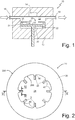
- FIG. 1 shows an apparatus 10 for growing a silicon-carbide wafer.
- the apparatus 10 comprises a body 12, a heater 14, an inlet duct 16, an outlet duct 18, a support 20 (also referred to as "susceptor") and a container 22, for example cup-shaped.
- the body 12 forms a reaction chamber 24 delimiting a closed space where the reactions take place.
- the susceptor 20 and the container 22 are positioned within the reaction chamber 24.
- the body 12 is generally of thermally insulating material, and thermally insulates the reaction chamber 24 from the external environment.
- the heater 14 is coupled to the body 12, for example arranged facing the reaction chamber 24.
- the heater 14 heats the reaction chamber 24 and what is contained inside the reaction chamber 24 (for example, the susceptor 20, the container 22, gas, substrates, wafers, or other objects or substances).
- the heater 14 may be produced in any way.
- the heater 14 may be an inductive heater that includes a plurality of coils; or a resistive heater that includes resistors covered with carbide or some other type of heating device.
- the inlet duct 16 provides a fluidic path from the environment external to the apparatus 10 to the reaction chamber 24 and can be used for introducing precursors and gas into the reaction chamber 24, as discussed below.
- the outlet duct 18 provides a fluidic path from the reaction chamber 24 to the outside of the apparatus 10. It may also be used for outside discharging reaction gases formed in the reaction chamber 24, as discussed below.
- the reaction chamber 24 is of a horizontal-flow type.
- the inlet duct 16 and the outlet duct 18 are horizontally aligned to each other and the gases flow longitudinally along a top surface of the susceptor 20.
- the susceptor 20 is arranged over the container 22 and in the reaction chamber 24.
- the susceptor 20 forms a platform for receiving and holding a substrate or a wafer, within the reaction chamber 24.
- a silicon substrate is arranged on the susceptor 20 during the manufacture of a SiC wafer.
- the susceptor 20 includes a frame 26 positioned above and supported by the container 22, to carry a substrate to be processed, here a monocrystalline silicon substrate, as discussed in detail with reference to Figures 8-12 ; an opening 28 surrounded and defined by the frame 26; and a plurality of arms 30 extending from the frame 26 towards the inside of the opening 28, for supporting the silicon substrate thereon.
- the container 22 is arranged in the reaction chamber 24, directly underneath the susceptor 20.
- the susceptor 20 rests on the container 22 so that the material being discharged through the opening 28 of the susceptor 20 during operation of the apparatus 10 (molten silicon) may be collected by the container 22.
- the container 22 includes a base 32 and a side wall 34.
- the base 32 extends directly underneath the opening 28 and the arms 30 of the susceptor 20.
- the base 32 carries a sponge 33, as described in US 2018/0090350 , cited above.
- the side wall 34 of the container 22 is arranged directly underneath the frame 26 of the susceptor 20.
- FIGS 2-6 show a susceptor 20 that may be used in the apparatus 10.
- the susceptor 20 includes the frame 26, the opening 28, and a plurality of arms 30, provided as a single piece.
- the frame 26 has a generally annulus shape, delimited externally by an outer wall 26A, internally by an inner wall 26B, at the top by a top surface 26C, and at the bottom by a bottom surface 26D.
- the outer wall 26A is here cylindrical and has a diameter correlated to the reaction chamber 24;
- the inner wall 26B has a generally cylindrical shape, the diameter whereof depends upon the size of the wafers that are to be obtained, just slightly larger than the wafer diameter, as explained below.
- the bottom surface 26D is carried by the container 22, and the top surface 26C, opposite to the bottom surface 26D, here defines a reference plane.
- the frame 26 moreover has a constant height H F , depending upon the used reaction chamber 24 and usually less than 1 cm, for example less than 0.5 cm.
- the frame 26 moreover has a plurality of projections 40 extending radially from the inside of the opening 28 towards the centre and at a uniform distance from each other.
- the frame 26 has eight projections 40, each delimited by arched walls 40A having convexity facing the opening 28 and by a transverse wall 40B extending between the arched walls 40A.
- the projections 40 here have the same thickness as the frame 26.
- the transverse walls 40B (of a planar or slightly arched shape) define, as a whole, an approximately cylindrical virtual wall having a diameter substantially equal to or, at the most, slightly larger than the diameter of the semiconductor wafer to be grown, as explained below.
- the projections 40 may be missing, in which case the cylindrical wall formed by the surface portions 40A coincides with the inner wall 26B of the frame.
- each arm 30 has a cross-section (according to a plane parallel to the planes tangential to the inner and outer surfaces 26A, 26B of the frame 26) shaped as a non-equilateral pentagon, as shown in Figure 6 .
- the cross-section of the arms 30 is here formed by a top portion 30A with a triangular-shaped and by a bottom portion 30B with an upside down-turned trapezium shape (with the major base forming the base of the triangular shape of the top portion 30A).
- each arm 30 is delimited by two top inclined sides 41, 42, and the bottom portion 30B of each arm 30 is delimited by two bottom inclined sides 45, 46 and by a bottom side 47.
- the two top inclined sides 41, 42 of each arm 30 join up (in the ideal representation of Figure 6 ) along a vertex line 43 even though, in a practical embodiment, the arms 40 have at the top a more or less rounded vertex portion surface.
- the top inclined sides 41, 42 have an inclination angle ⁇ (with respect to a plane passing through the bases of the top portion 30A and bottom portion 30B) that is smaller than the bottom inclined sides 45, 46 (inclination angle ⁇ ), thus favouring flow of molten material, as explained in detail hereinafter with reference to the manufacturing process represented in Figures 8-12 .
- the arms 30 In longitudinal section, along the vertex line 43 (shown in Figure 5 ), the arms 30 have a constant height H A , smaller than height H F of the frame 26.
- distance d H F - H A is approximately equal to a height of a substrate to be inserted into the frame 26, as discussed in detail hereinafter.
- the distance d may be at least 60-70 ⁇ m, in particular comprised between 200 and 300 ⁇ m.
- the arms 30 moreover all have the same length L, starting from the projections 40.
- the arms 30 may have a length L comprised between 11 mm and 13 mm, for example approximately 12 mm; a height H A depending upon the geometry of the reaction chamber and comprised, for example, between 0.3 and 0.7 cm, in particular approximately 0.5 cm; a height H1 of the top portion 30A greater than the height H2 of the bottom portion 30B; maximum inclination angles ⁇ and ⁇ according to the limits imposed by the manufacturer, where the sum ⁇ + ⁇ may be comprised between 110° and 150° (where in general ⁇ > ⁇ , as mentioned above).
- the vertex lines 43 of the arms 30 define a virtual resting surface 44 that, together with the wall defined by the side surfaces 40B of the projections 40, forms a lowered seat 48 for a semiconductor wafer to be grown, as explained in detail hereinafter with reference to Figures 8-12 .
- the susceptor 20, and in particular the arms 30, may be coated with a coating (not shown) that counters adhesion of any possible material (in particular, molten silicon, as discussed below).
- the coating may be of silicon carbide, as described in US 2018/0090350 referred to above.
- FIG. 7 shows a susceptor 120 designed for manufacturing wafers of 6" diameter.
- the susceptor 120 of Figure 7 has a general structure similar to the susceptor 20 of Figure 2 , with arms 130 orientated towards the inside of the opening (here designated by 128), but the opening 128, and in particular the cylindrical wall formed by the surface portions (here designated by 140A) of the projections (here 140) has larger dimensions, to be able to receive the wafer.
- Figures 8 to 12 show an embodiment of a process for manufacturing a silicon carbide wafer, in particular a SiC-3C wafer, using the apparatus 10 of Figure 1 .
- the body 12, the heater 14, the inlet duct 16, and the outlet duct 18 are not shown, for simplicity.
- a substrate 58 of a first material here a silicon substrate
- the substrate 58 is inserted, almost force-fitted, into the seat 48, with its own edge 58A in contact with the surface portions 40B of the projections 40, on the arms 30, so that its bottom surface 58B is in contact with the vertex 43 of the top portions 30A of the arms 30, on the virtual resting surface 44.
- the substrate 58 has a thickness that is as thin as possible, compatibly with brittleness.
- the substrate 58 may have a thickness of at least 60-70 ⁇ m, in particular comprised between 200 ⁇ m and 300 ⁇ m.
- the top surface of the latter sets approximately level with the reference plane formed by the top surface 26C of the frame 26, and the substrate 58 does not project substantially in height from the opening 28.
- the substrate 58 generally has a crystalline structure. Moreover, in this step, the reaction chamber 24 is at room temperature.
- the reaction chamber 24 is sealed and heated by the heater 14 to a first temperature.
- the first temperature may be comprised between 450°C and 550°C.
- a first pressure level for example comprised between 8 ⁇ 10 -5 and 12 ⁇ 10 -5 bar, is set in the reaction chamber 24.
- the reaction chamber 24 After the reaction chamber 24 has been heated to the first temperature, it is brought to a second temperature, higher than the first temperature.
- the second temperature may be comprised between 1050°C and 1150°C.
- the reaction chamber 24 is kept at the second pressure level for the rest of the process.
- the substrate 58 is immersed in hydrogen (H 2 ). Hydrogen is introduced into the reaction chamber 24 through the inlet duct 16. Moreover, the substrate 58 is subjected to activation operations by introducing hydrochloric acid (HCl) into the reaction chamber 24 through the inlet duct 16.
- H 2 hydrogen
- HCl hydrochloric acid
- the reaction chamber 10 is then heated by the heater 14 to a third temperature, higher than the second temperature.
- the third temperature is comprised between 1340°C and 1400°C.
- a carbon-based precursor is introduced into the reaction chamber 24 through the inlet duct 16.
- the carbon-based precursor carbonises the surface silicon atoms of the substrate 58 to form a thin SiC layer, as 3C-SiC, having a thickness, for example, in the region of a few nanometres. This is frequently referred to as ramp carbonisation.
- the thin SiC layer acts as seed for growing SiC.
- the constant distribution of the temperature is also favoured by the fact that, in this step, as in the subsequent growing steps and in the preliminary heating steps, in a per se known and not shown manner, the susceptor 20 is made to turn within the reaction chamber 24. In this way, the substrate 58 is lapped by the introduced gases, starting from the entire circumference, and therefore in a way as uniform as possible during growth.
- a silicon-based precursor is added to the carbon-based precursor in the reaction chamber 24. Consequently, a first SiC layer 60 starts to grow in an epitaxial way from the thin SiC layer, as shown in Figure 9 . This step is frequently defined as hetero-epitaxial growth.
- a melting process is carried out.
- the reaction chamber 24 is heated by the heater 14 up to a fourth temperature, higher than the melting point of the substrate 58 and lower than the melting point of the first SiC layer 60.
- the fourth temperature is comprised between 1550°C and 1650°C. Consequently, as shown in Figure 10 , the substrate 58 melts and deposits in the container 22, being absorbed by the sponge 33.
- the molten silicon (designated by 66 in Figure 10 ) coming from the substrate 58 flows along the top inclined sides 41, 42 of the arms 30, flows along the bottom inclined sides 45, 46 of the arms 30, and drops from the susceptor 20 onto the bottom of the container 22, where it is collected and absorbed by the sponge 33.
- the minimum area of contact between the susceptor 20 and the substrate 58 (at the vertex 43 of the top portion 30A of the arms 30) and the inclination of the top and bottom inclined sides 41, 42, 45, 46 favour flow of the molten silicon 66 from the substrate 58.
- the surface tension between the susceptor 20 and the molten silicon 66 is reduced.
- the presence of the bottom inclined sides 45, 46 favours dropping of the molten silicon 66 from the top inclined sides 41, 42 directly downwards. Consequently, it is less likely for the molten silicon 66 to attach or adhere to the arms 30; instead, it tends to detach from the susceptor 20 and to flow towards the bottom of the container 22.
- top inclined sides 41, 42 extend throughout the length of the arms 30 enables detachment of the molten silicon 66 from the entire bottom surface 58A of the substrate 58.
- the reaction chamber 24 can be maintained at the fourth temperature until all the substrate 58 is removed from the first SiC layer 60.
- the fourth temperature of the reaction chamber 24 can be maintained until small portions or a thin residual layer 70 of the substrate 58 remain/remains on the susceptor 20.
- the residual layer 70 of the substrate 58 is removed by a chemical-etching process.
- a silicon- and carbon-based precursor is introduced into the reaction chamber 24 through the inlet duct 16. Therefore, the first SiC layer 60 continues to grow in thickness; i.e., a second SiC layer 68 starts to grow on the first SiC layer 60. This step is frequently referred to as homo-epitaxial growth.
- the silicon- and carbon-based precursor can be supplied during the the substrate 58 melting step. Alternatively, the silicon- and carbon-based precursor is supplied after the process of melting of the substrate 58 is completed.
- the SiC wafer contains residual portions 70 of the substrate 58, these are removed via a chemical-etching process during growth of the second SiC layer 68 or at the end of such growth.
- a chemical-etching gas such as hydrochloric acid (HCl)
- HCl hydrochloric acid
- the reaction chamber 10 is turned off, vented, and brought back to a lower temperature (e.g., room temperature) .
- the resulting SiC wafer 72 can then be immersed in H 2 or Ar.
- Figure 13 shows a SiC wafer 72 thus obtained on the susceptor 20.
- SiC wafers of large dimensions even larger than 6", for example 8", up to 12", even though the process and apparatus operate reliably and advantageously also for the manufacture of wafers of smaller dimensions, such as 2", 4 and 6" wafers.
Landscapes
- Chemical & Material Sciences (AREA)
- Metallurgy (AREA)
- Engineering & Computer Science (AREA)
- Materials Engineering (AREA)
- Organic Chemistry (AREA)
- General Chemical & Material Sciences (AREA)
- Chemical Kinetics & Catalysis (AREA)
- Crystallography & Structural Chemistry (AREA)
- Mechanical Engineering (AREA)
- Inorganic Chemistry (AREA)
- Crystals, And After-Treatments Of Crystals (AREA)
- Chemical Vapour Deposition (AREA)
- Recrystallisation Techniques (AREA)
Abstract
Description
- The present invention relates to an apparatus for growing a semiconductor wafer, in particular of silicon carbide, and to an associated manufacturing process.
- As is known, semiconductor devices are typically manufactured in silicon wafers. However, silicon-carbide (SiC) wafers have become increasingly popular due, at least in part, to the favourable chemico-physical properties of SiC. For instance, SiC generally has a wider band gap than silicon. Consequently, SiC, also with relatively thin thicknesses, has a higher breakdown voltage than silicon and may therefore be advantageously used in high-voltage applications, such as in power devices.
- Silicon carbide exists in different crystallographic forms or polytypes. The most common polytypes are the cubic polytype (polytype 3C-3C-SiC), the hexagonal polytype (polytypes 4H-SiC and 6H-SiC) and the rhombohedral polytype (polytype 15R-SiC). Amongst these, currently the cubic polytype 3C-SiC has been the subject of in-depth study, due to its unique properties as compared to other wafer polytypes. For instance, generally 3C-SiC wafers have a lower trap density on the SiO2/3C-SiC interface and a greater channel-electrons mobility. Other interesting characteristics of 3C-SiC are the low value of ON-state resistance Ron, which is particularly useful in case of devices working up to and beyond 650 V.
- However, manufacturing of silicon-carbide wafers is more complex than that of silicon wafers and, currently, 3C-SiC substrates are not available on the market.
- An apparatus and a method for manufacturing a SiC silicon-carbide wafer are described in the
US 2013/0157448 entitled "Method for manufacturing a silicon carbide wafer and respective equipment", filed in the name of the present applicant. This patent application describes a method for manufacturing the SiC wafer including positioning a silicon substrate on a support (referred to as "susceptor") in a reaction chamber, growing a 3C-SiC epitaxial layer on the silicon substrate, and then separating the silicon substrate from the 3C-SiC epitaxial layer by melting the silicon substrate. The molten silicon is then drained off through a pair of discharge openings underneath the susceptor. - To improve the separation of the silicon substrate from the 3C-SiC epitaxial layer, the present applicant has developed an improved reaction chamber, described in
US 2018/0090350 and entitled "Apparatus for manufacturing a silicon carbide wafer". Here, the susceptor is formed by a plurality of bars having a tilted shape or facing downwards to favour the flow of the molten silicon through the openings between the bars. Moreover, a sponge is arranged in a cup-shaped container, underneath the support to collect the molten silicon and simplify the removal thereof from the reaction chamber. However, also this solution has proven not always able to drain off the molten silicon properly into the collection tank, since, at times, the molten silicon attaches and adheres to the susceptor because of the surface tension between them. - A further improvement is described in
US patent application SN 16/182050 filed on 6 November 2018 - However, not even the susceptor described in US
patent application SN 16/182050 -
US 2009/0255901 discloses a plasma processing apparatus including a tray for temporarily supporting wafers to be processed while moving from a load chamber to a processing chamber. Here, a susceptor has a dielectric plate that includes substrate placement portions and is raised for supporting the wafers during processing. In an embodiment the tray has projecting portions supporting the wafers and intended for centering the dielectric plate. -
US 2008/069951 discloses an apparatus for epitaxial deposition comprising a wafer holding structure having fingers defining contact points. - The aim of the present invention is to provide an improved apparatus and process that overcome the drawbacks of the prior art and enable manufacture of silicon-carbide wafers, even of large dimensions.
- According to the present invention, an apparatus and a process for growing a silicon-carbide wafer are provided, as defined in the attached claims.
- In practice, the present apparatus comprises a support formed by a frame, an opening in the frame, and by a plurality of arms extending into the opening, towards the centre thereof. The arms define a resting surface for a wafer that is at a lower level than the frame.
- In fact, studies conducted by the present applicant have shown that, during SiC growing, obtained by induction in a CVD (Chemical-Vapour Deposition) type reactor on the silicon substrate, the distribution of the heat within the reaction chamber is not uniform, but the edge of the wafer is colder than the centre by a few tens of degrees. The present applicant has supposed that this temperature gradient is due to the instability of the flow of the growth gases, which should lap, in a laminar way, the initial silicon wafer and the first thin SiC layer growing on the silicon substrate. Since the initial silicon wafer is at higher level and projects from the substrate, it has been supposed that this causes an instability in the growth gas flow, and consequently a temperature gradient is generated.
- To solve the above problem, then, the support is manufactured so that the supporting arms are arranged at a lower level than the frame and the initial silicon wafer is arranged within the frame so that its top surface is approximately aligned with that of the frame.
- For a better understanding of the present invention, embodiments thereof are now described, purely by way of nonlimiting example, with reference to the attached drawings, wherein:
-
Figure 1 is a cross-section of an embodiment of the present apparatus; -
Figure 2 is a top view of an embodiment of a support usable in the apparatus ofFigure 1 ; -
Figure 3 is a perspective view from above of the support ofFigure 2 ; -
Figure 4 is an enlarged perspective view of a detail of the support ofFigure 2 ; -
Figure 5 is a cross-section of the support ofFigure 2 , taken along section line V-V ofFigure 2 ; -
Figure 6 is a cross-section through a part of the support ofFigure 2 , taken along section line VI-VI ofFigure 2 ; -
Figure 7 is a top view of another embodiment of a support usable in the apparatus ofFigure 1 ; -
Figures 8-12 are cross-sections showing successive steps for manufacturing a semiconductor wafer using the apparatus ofFigure 1 ; and -
Figure 13 is a perspective view of the substrate ofFigures 2-4 with a semiconductor wafer obtained at the end of the manufacturing process. -
Figure 1 shows anapparatus 10 for growing a silicon-carbide wafer. Theapparatus 10 comprises abody 12, aheater 14, aninlet duct 16, anoutlet duct 18, a support 20 (also referred to as "susceptor") and acontainer 22, for example cup-shaped. - The
body 12 forms areaction chamber 24 delimiting a closed space where the reactions take place. Thesusceptor 20 and thecontainer 22 are positioned within thereaction chamber 24. Thebody 12 is generally of thermally insulating material, and thermally insulates thereaction chamber 24 from the external environment. - The
heater 14 is coupled to thebody 12, for example arranged facing thereaction chamber 24. Theheater 14 heats thereaction chamber 24 and what is contained inside the reaction chamber 24 (for example, thesusceptor 20, thecontainer 22, gas, substrates, wafers, or other objects or substances). Theheater 14 may be produced in any way. For instance, theheater 14 may be an inductive heater that includes a plurality of coils; or a resistive heater that includes resistors covered with carbide or some other type of heating device. - The
inlet duct 16 provides a fluidic path from the environment external to theapparatus 10 to thereaction chamber 24 and can be used for introducing precursors and gas into thereaction chamber 24, as discussed below. - The
outlet duct 18 provides a fluidic path from thereaction chamber 24 to the outside of theapparatus 10. It may also be used for outside discharging reaction gases formed in thereaction chamber 24, as discussed below. - In particular, in the
apparatus 10, thereaction chamber 24 is of a horizontal-flow type. To this end, as shown, for example, inFigure 1 , theinlet duct 16 and theoutlet duct 18 are horizontally aligned to each other and the gases flow longitudinally along a top surface of thesusceptor 20. - The
susceptor 20 is arranged over thecontainer 22 and in thereaction chamber 24. Thesusceptor 20 forms a platform for receiving and holding a substrate or a wafer, within thereaction chamber 24. In particular, as discussed below, a silicon substrate is arranged on thesusceptor 20 during the manufacture of a SiC wafer. - As discussed in detail hereinafter with reference to
Figures 2-7 , thesusceptor 20 includes aframe 26 positioned above and supported by thecontainer 22, to carry a substrate to be processed, here a monocrystalline silicon substrate, as discussed in detail with reference toFigures 8-12 ; an opening 28 surrounded and defined by theframe 26; and a plurality ofarms 30 extending from theframe 26 towards the inside of theopening 28, for supporting the silicon substrate thereon. - The
container 22 is arranged in thereaction chamber 24, directly underneath thesusceptor 20. Thesusceptor 20 rests on thecontainer 22 so that the material being discharged through theopening 28 of thesusceptor 20 during operation of the apparatus 10 (molten silicon) may be collected by thecontainer 22. Thecontainer 22 includes abase 32 and aside wall 34. Thebase 32 extends directly underneath theopening 28 and thearms 30 of thesusceptor 20. The base 32 carries asponge 33, as described inUS 2018/0090350 , cited above. Theside wall 34 of thecontainer 22 is arranged directly underneath theframe 26 of thesusceptor 20. -
Figures 2-6 show asusceptor 20 that may be used in theapparatus 10. - In detail, as mentioned above, the
susceptor 20 includes theframe 26, theopening 28, and a plurality ofarms 30, provided as a single piece. - The
frame 26 has a generally annulus shape, delimited externally by anouter wall 26A, internally by aninner wall 26B, at the top by atop surface 26C, and at the bottom by abottom surface 26D. Theouter wall 26A is here cylindrical and has a diameter correlated to thereaction chamber 24; theinner wall 26B has a generally cylindrical shape, the diameter whereof depends upon the size of the wafers that are to be obtained, just slightly larger than the wafer diameter, as explained below. Thebottom surface 26D is carried by thecontainer 22, and thetop surface 26C, opposite to thebottom surface 26D, here defines a reference plane. Theframe 26 moreover has a constant height HF, depending upon the usedreaction chamber 24 and usually less than 1 cm, for example less than 0.5 cm. - The
frame 26 moreover has a plurality ofprojections 40 extending radially from the inside of theopening 28 towards the centre and at a uniform distance from each other. In the embodiment ofFigures 2-6 , for instance, theframe 26 has eightprojections 40, each delimited byarched walls 40A having convexity facing theopening 28 and by atransverse wall 40B extending between thearched walls 40A. Theprojections 40 here have the same thickness as theframe 26. Thetransverse walls 40B (of a planar or slightly arched shape) define, as a whole, an approximately cylindrical virtual wall having a diameter substantially equal to or, at the most, slightly larger than the diameter of the semiconductor wafer to be grown, as explained below. - The
projections 40 may be missing, in which case the cylindrical wall formed by thesurface portions 40A coincides with theinner wall 26B of the frame. - The
arms 30 are bar-shaped, linear, extend in cantilever fashion from theprojections 40, one for each projection, radially towards the centre of theopening 28, and have afree end 31 suspended over thecontainer 22. In detail, here eacharm 30 has a cross-section (according to a plane parallel to the planes tangential to the inner andouter surfaces Figure 6 . Specifically, the cross-section of thearms 30 is here formed by atop portion 30A with a triangular-shaped and by abottom portion 30B with an upside down-turned trapezium shape (with the major base forming the base of the triangular shape of thetop portion 30A). In practice, thetop portion 30A of eacharm 30 is delimited by two topinclined sides bottom portion 30B of eacharm 30 is delimited by two bottominclined sides bottom side 47. The two topinclined sides arm 30 join up (in the ideal representation ofFigure 6 ) along avertex line 43 even though, in a practical embodiment, thearms 40 have at the top a more or less rounded vertex portion surface. - In the embodiment shown, the top
inclined sides top portion 30A andbottom portion 30B) that is smaller than the bottom inclined sides 45, 46 (inclination angle β), thus favouring flow of molten material, as explained in detail hereinafter with reference to the manufacturing process represented inFigures 8-12 . - In longitudinal section, along the vertex line 43 (shown in
Figure 5 ), thearms 30 have a constant height HA, smaller than height HF of theframe 26. In particular, distance d = HF - HA is approximately equal to a height of a substrate to be inserted into theframe 26, as discussed in detail hereinafter. For instance, the distance d may be at least 60-70 µm, in particular comprised between 200 and 300 µm. - The
arms 30 moreover all have the same length L, starting from theprojections 40. - In particular, the
arms 30 may have a length L comprised between 11 mm and 13 mm, for example approximately 12 mm; a height HA depending upon the geometry of the reaction chamber and comprised, for example, between 0.3 and 0.7 cm, in particular approximately 0.5 cm; a height H1 of thetop portion 30A greater than the height H2 of thebottom portion 30B; maximum inclination angles α and β according to the limits imposed by the manufacturer, where the sum α + β may be comprised between 110° and 150° (where in general β > α, as mentioned above). - The vertex lines 43 of the
arms 30 define avirtual resting surface 44 that, together with the wall defined by the side surfaces 40B of theprojections 40, forms a loweredseat 48 for a semiconductor wafer to be grown, as explained in detail hereinafter with reference toFigures 8-12 . - The
susceptor 20, and in particular thearms 30, may be coated with a coating (not shown) that counters adhesion of any possible material (in particular, molten silicon, as discussed below). For instance, the coating may be of silicon carbide, as described inUS 2018/0090350 referred to above. -
Figure 7 shows asusceptor 120 designed for manufacturing wafers of 6" diameter. Thesusceptor 120 ofFigure 7 has a general structure similar to thesusceptor 20 ofFigure 2 , witharms 130 orientated towards the inside of the opening (here designated by 128), but the opening 128, and in particular the cylindrical wall formed by the surface portions (here designated by 140A) of the projections (here 140) has larger dimensions, to be able to receive the wafer. -
Figures 8 to 12 show an embodiment of a process for manufacturing a silicon carbide wafer, in particular a SiC-3C wafer, using theapparatus 10 ofFigure 1 . In these figures, thebody 12, theheater 14, theinlet duct 16, and theoutlet duct 18 are not shown, for simplicity. Moreover, again for simplicity, reference will be made to thesusceptor 20 ofFigures 2-6 , but what mentioned also applies to thesusceptor 120 ofFigure 7 . - In detail (
Figure 8 ), asubstrate 58 of a first material, here a silicon substrate, is positioned in thereaction chamber 24, and precisely in theseat 48 of thesusceptor 20. Thesubstrate 58 is inserted, almost force-fitted, into theseat 48, with itsown edge 58A in contact with thesurface portions 40B of theprojections 40, on thearms 30, so that itsbottom surface 58B is in contact with thevertex 43 of thetop portions 30A of thearms 30, on thevirtual resting surface 44. - The
substrate 58 has a thickness that is as thin as possible, compatibly with brittleness. For instance, thesubstrate 58 may have a thickness of at least 60-70 µm, in particular comprised between 200 µm and 300 µm. - As mentioned above, since the distance d between the
virtual resting surface 44 and thereference plane 26C is approximately equal to the thickness of thesubstrate 58, the top surface of the latter sets approximately level with the reference plane formed by thetop surface 26C of theframe 26, and thesubstrate 58 does not project substantially in height from theopening 28. - The
substrate 58 generally has a crystalline structure. Moreover, in this step, thereaction chamber 24 is at room temperature. - Once the
substrate 58 is positioned in thesusceptor 20, thereaction chamber 24 is sealed and heated by theheater 14 to a first temperature. For instance, the first temperature may be comprised between 450°C and 550°C. Moreover a first pressure level, for example comprised between 8·10-5 and 12·10-5 bar, is set in thereaction chamber 24. - After the
reaction chamber 24 has been heated to the first temperature, it is brought to a second temperature, higher than the first temperature. For instance, the second temperature may be comprised between 1050°C and 1150°C. Moreover a second pressure level, higher than the first pressure level, for example comprised between 75 and 125 mbar, is set in thereaction chamber 24. - The
reaction chamber 24 is kept at the second pressure level for the rest of the process. - After the
reaction chamber 24 has been heated to the second temperature, thesubstrate 58 is immersed in hydrogen (H2). Hydrogen is introduced into thereaction chamber 24 through theinlet duct 16. Moreover, thesubstrate 58 is subjected to activation operations by introducing hydrochloric acid (HCl) into thereaction chamber 24 through theinlet duct 16. - The
reaction chamber 10 is then heated by theheater 14 to a third temperature, higher than the second temperature. For instance, the third temperature is comprised between 1340°C and 1400°C. - Again with reference to
Figure 8 , while thereaction chamber 24 is brought to the third temperature or after it has reached the third temperature, a carbon-based precursor is introduced into thereaction chamber 24 through theinlet duct 16. The carbon-based precursor carbonises the surface silicon atoms of thesubstrate 58 to form a thin SiC layer, as 3C-SiC, having a thickness, for example, in the region of a few nanometres. This is frequently referred to as ramp carbonisation. As will be discussed hereinafter, the thin SiC layer acts as seed for growing SiC. - In this step, due to the arrangement of the
substrate 58 within theseat 48, with its top surface flush with thetop surface 26C of theframe 26, the gases flow, lapping the substrate 58 (or the wafer being grown) with an approximately laminar motion. This makes it possible to have a more uniform flow of gases and a distribution of temperature more constant as compared known apparatuses. - The constant distribution of the temperature is also favoured by the fact that, in this step, as in the subsequent growing steps and in the preliminary heating steps, in a per se known and not shown manner, the
susceptor 20 is made to turn within thereaction chamber 24. In this way, thesubstrate 58 is lapped by the introduced gases, starting from the entire circumference, and therefore in a way as uniform as possible during growth. - When the
reaction chamber 24 is at the third temperature, a silicon-based precursor is added to the carbon-based precursor in thereaction chamber 24. Consequently, afirst SiC layer 60 starts to grow in an epitaxial way from the thin SiC layer, as shown inFigure 9 . This step is frequently defined as hetero-epitaxial growth. - Next, maintaining a flow of H2 in the
reaction chamber 24 through theinlet duct 16, a melting process is carried out. In particular, thereaction chamber 24 is heated by theheater 14 up to a fourth temperature, higher than the melting point of thesubstrate 58 and lower than the melting point of thefirst SiC layer 60. For instance, the fourth temperature is comprised between 1550°C and 1650°C. Consequently, as shown inFigure 10 , thesubstrate 58 melts and deposits in thecontainer 22, being absorbed by thesponge 33. In particular, the molten silicon (designated by 66 inFigure 10 ) coming from thesubstrate 58 flows along the topinclined sides arms 30, flows along the bottom inclined sides 45, 46 of thearms 30, and drops from thesusceptor 20 onto the bottom of thecontainer 22, where it is collected and absorbed by thesponge 33. - In this step, the minimum area of contact between the susceptor 20 and the substrate 58 (at the
vertex 43 of thetop portion 30A of the arms 30) and the inclination of the top and bottom inclined sides 41, 42, 45, 46 favour flow of themolten silicon 66 from thesubstrate 58. In fact, when thesubstrate 58 is molten, the surface tension between the susceptor 20 and themolten silicon 66 is reduced. Moreover, the presence of the bottom inclined sides 45, 46 favours dropping of themolten silicon 66 from the topinclined sides molten silicon 66 to attach or adhere to thearms 30; instead, it tends to detach from thesusceptor 20 and to flow towards the bottom of thecontainer 22. - The fact that the top
inclined sides arms 30 enables detachment of themolten silicon 66 from the entirebottom surface 58A of thesubstrate 58. - The
reaction chamber 24 can be maintained at the fourth temperature until all thesubstrate 58 is removed from thefirst SiC layer 60. - Alternatively, as shown in
Figure 10 , the fourth temperature of thereaction chamber 24 can be maintained until small portions or a thinresidual layer 70 of thesubstrate 58 remain/remains on thesusceptor 20. In this embodiment, as discussed hereinafter with reference toFigure 12 , theresidual layer 70 of thesubstrate 58 is removed by a chemical-etching process. - In
Figure 11 , a silicon- and carbon-based precursor is introduced into thereaction chamber 24 through theinlet duct 16. Therefore, thefirst SiC layer 60 continues to grow in thickness; i.e., asecond SiC layer 68 starts to grow on thefirst SiC layer 60. This step is frequently referred to as homo-epitaxial growth. The silicon- and carbon-based precursor can be supplied during the thesubstrate 58 melting step. Alternatively, the silicon- and carbon-based precursor is supplied after the process of melting of thesubstrate 58 is completed. - When the
second SiC layer 68 reaches a desired thickness, the flow of the silicon- and carbon-based precursor is stopped. Possible reaction gases in thereaction chamber 24 are removed from thereaction chamber 24 through the outlet duct 18 (Figure 1 ). - As mentioned previously, if the SiC wafer contains
residual portions 70 of thesubstrate 58, these are removed via a chemical-etching process during growth of thesecond SiC layer 68 or at the end of such growth. In this case, a chemical-etching gas, such as hydrochloric acid (HCl), is introduced into thereaction chamber 24 through the inlet duct 16 (Figure 1 ). Theresidual portions 70 of thesubstrate 58 once again coupled to thefirst SiC layer 60 are therefore removed by the chemical-etching gas and generally removed through the outlet duct 18 (Figure 12 ). - Once the
residual portions 70 of thesubstrate 58 have been removed, thereaction chamber 10 is turned off, vented, and brought back to a lower temperature (e.g., room temperature) . The resultingSiC wafer 72 can then be immersed in H2 or Ar. -
Figure 13 shows aSiC wafer 72 thus obtained on thesusceptor 20. - Therefore, with the described apparatus and process, since the
frame 26 is very close to the wafer that is being grown and this, initially, does not project at the top from the susceptor, it is possible to obtain a better temperature distribution and to reduce flow instability, enabling growth of SiC wafers that are substantially monocrystalline throughout their diameter and without polycrystalline edge areas. - Moreover, by virtue of the shape of the
arms 30 and to their limited number, detachment of the silicon can come about in a more reliable and complete way as compared to known solutions. - Consequently, it becomes possible to manufacture SiC wafers of large dimensions, even larger than 6", for example 8", up to 12", even though the process and apparatus operate reliably and advantageously also for the manufacture of wafers of smaller dimensions, such as 2", 4 and 6" wafers.
- Finally, it is clear that modifications and variations may be made to the apparatus and to the process described and shown herein, without thereby departing from the scope of the present invention, as defined in the attached claims. For instance, the various embodiments described may be combined so as to provide further solutions.
Claims (12)
- An apparatus (10) for growing wafers of semiconductor material, in particular of silicon carbide, comprising:a chamber (24);a collection container (22) in the chamber; anda support or susceptor (20) in the chamber and over the collection container, the support (20) including a frame (26), an opening (28) surrounded by the frame, a plurality of arms (30) and a seat (48) within the opening (28),wherein the frame (26) has a first surface (26D) and a second surface (26C), opposite to each other, the first surface (26D) of the frame directly facing the collection container (22);the arms (30) are formed by cantilever bars extending from the frame (26) into the opening (28), having a maximum height smaller than the frame and having at the top a resting edge (43), the resting edges of the arms defining a resting surface (44) that is at a lower level than the second surface (26C) of the frame; andthe seat (48) has a bottom formed by the resting surface (44) .
- The apparatus according to claim 1, wherein the resting surface (44) is arranged at a distance (d) from the second surface (26C) of the frame (26) equal to the height of a substrate (58) to be inserted in use into the seat (48).
- The apparatus according to claim 1 or claim 2, wherein the resting surface (44) is arranged at a distance (d) from the second surface (26C) of the frame (26).
- The apparatus according to any of the preceding claims, wherein each arm (30) is upwardly delimited by at least one inclined side (41, 42), the inclined side of each arm having a non-zero inclination with respect to the resting surface (44).
- The apparatus according to any of claims 1-3, wherein each arm (30) is upwardly delimited by a pair of top inclined sides (41, 42), that are contiguous and join up to form a vertex line (43) belonging to the resting surface (44).
- The apparatus according to any of the preceding claims, wherein each arm (30) is downwardly delimited by a pair of bottom inclined sides (45, 46).
- The apparatus according to the preceding claim, wherein the arms (30) have a pentagonal cross-section.
- The apparatus according to claim 6 or 7, wherein the bottom inclined sides (45, 46) have an inclination, with respect to a plane parallel to the resting surface (44), greater than the top inclined sides (41, 42).
- The apparatus according to any of the preceding claims, further comprising a plurality of projections (40) extending from the frame (26) into the opening (28), each projection (40) having connection walls (40A) extending transversely from the frame (26), and a transverse wall (40B) extending between the connection walls (40A), the transverse walls (40B) forming, together with the resting surface (44), the seat (48),
wherein each arm (30) extends from a respective transverse wall (40B). - A manufacturing process, using the apparatus according to any of the preceding claims, the apparatus comprising:a chamber (24);a collection container (22) in the chamber;a support or susceptor (20) in the chamber and over the collection container, the support including a frame (26), an opening (28) surrounded by the frame, a plurality of arms (30), and a seat (48) within the opening;wherein the frame (26) has a first and a second surface (26D, 26C), opposite to each other, the first surface (26D) of the frame facing the collection container (22); the arms (30) are formed by cantilever bars extending from the frame (26) into the opening (28), having a maximum height smaller than the frame, and having at the top a resting edge (43), the resting edges of the arms defining a resting surface (44) at a lower level than the second surface (26C) of the frame; and the seat (48) has a bottom formed by the resting surface (44),the process comprising:introducing a substrate (58) of a first material into the seat (48) to arrange the substrate (58) approximately flush with the frame (26);forming a layer (60) of a second material on the substrate, the layer of the second material having a first thickness;successively separating at least one first portion of the substrate (66) from the layer (60) of the second material, melting the first portion of the substrate (58); andgrowing the layer (60) of the second material until the layer of the second material has a second thickness, thicker than the first thickness.
- The process according to the preceding claim, further comprising, after growing the layer (60) of the second material, separating a second portion (70) of the substrate from the layer (60) of the second material by chemical etching.
- The process according to either claim 10 or 11, wherein the second material includes silicon carbide, and the first material includes silicon.
Applications Claiming Priority (1)
| Application Number | Priority Date | Filing Date | Title |
|---|---|---|---|
| IT102019000015416A IT201900015416A1 (en) | 2019-09-03 | 2019-09-03 | APPARATUS FOR GROWING A SLICE OF SEMICONDUCTOR MATERIAL, IN PARTICULAR SILICON CARBIDE, AND ASSOCIATED MANUFACTURING PROCESS |
Publications (2)
| Publication Number | Publication Date |
|---|---|
| EP3789520A1 true EP3789520A1 (en) | 2021-03-10 |
| EP3789520B1 EP3789520B1 (en) | 2022-06-29 |
Family
ID=68988226
Family Applications (1)
| Application Number | Title | Priority Date | Filing Date |
|---|---|---|---|
| EP20194374.3A Active EP3789520B1 (en) | 2019-09-03 | 2020-09-03 | Apparatus for growing a semiconductor wafer, in particular of silicon carbide, and associated manufacturing process |
Country Status (4)
| Country | Link |
|---|---|
| US (2) | US11692283B2 (en) |
| EP (1) | EP3789520B1 (en) |
| CN (2) | CN212750852U (en) |
| IT (1) | IT201900015416A1 (en) |
Families Citing this family (2)
| Publication number | Priority date | Publication date | Assignee | Title |
|---|---|---|---|---|
| US11309177B2 (en) | 2018-11-06 | 2022-04-19 | Stmicroelectronics S.R.L. | Apparatus and method for manufacturing a wafer |
| IT201900015416A1 (en) * | 2019-09-03 | 2021-03-03 | St Microelectronics Srl | APPARATUS FOR GROWING A SLICE OF SEMICONDUCTOR MATERIAL, IN PARTICULAR SILICON CARBIDE, AND ASSOCIATED MANUFACTURING PROCESS |
Citations (4)
| Publication number | Priority date | Publication date | Assignee | Title |
|---|---|---|---|---|
| US20080069951A1 (en) | 2006-09-15 | 2008-03-20 | Juan Chacin | Wafer processing hardware for epitaxial deposition with reduced auto-doping and backside defects |
| US20090255901A1 (en) | 2005-10-12 | 2009-10-15 | Shogo Okita | Plasma processing apparatus, plasma processing method, and tray |
| US20130157448A1 (en) | 2011-12-15 | 2013-06-20 | Stmicroelectronics S.R.L. | Method for manufacturing a silicon carbide wafer and respective equipment |
| US20180090350A1 (en) | 2016-09-28 | 2018-03-29 | Stmicroelectronics S.R.L. | Apparatus for manufacturing a silicon carbide wafer |
Family Cites Families (66)
| Publication number | Priority date | Publication date | Assignee | Title |
|---|---|---|---|---|
| US3108818A (en) | 1959-12-14 | 1963-10-29 | Felt Products Mfg Co | Fluid transfer seal for gasket |
| US3777009A (en) | 1971-08-05 | 1973-12-04 | Little Inc A | Method for direct melt synthesis of intermetallic compounds |
| US3922712A (en) | 1974-05-01 | 1975-11-25 | Gen Motors Corp | Plastic power semiconductor flip chip package |
| US4582561A (en) | 1979-01-25 | 1986-04-15 | Sharp Kabushiki Kaisha | Method for making a silicon carbide substrate |
| US4537651A (en) | 1981-05-22 | 1985-08-27 | United Technologies Corporation | Method for removing semiconductor layers from salt substrates |
| US4574730A (en) | 1984-02-27 | 1986-03-11 | Northern Telecom Limited | Melt dispensing liquid phase epitaxy boat |
| JPS61150366A (en) | 1984-12-25 | 1986-07-09 | Nec Corp | Mis type memory cell |
| IL98530A (en) | 1990-06-25 | 1996-06-18 | Lanxide Technology Co Ltd | Methods for making selfsupporting composite bodies and articles produced thereby using vapor-phase parent metals and solid oxidants |
| US5183529A (en) | 1990-10-29 | 1993-02-02 | Ford Motor Company | Fabrication of polycrystalline free-standing diamond films |
| JPH05208900A (en) | 1992-01-28 | 1993-08-20 | Nisshin Steel Co Ltd | Apparatus for growing silicon carbide single crystal |
| US5923408A (en) | 1996-01-31 | 1999-07-13 | Canon Kabushiki Kaisha | Substrate holding system and exposure apparatus using the same |
| FR2775328B1 (en) | 1998-02-26 | 2000-04-28 | Christian Loth | SEAL FOR PIPE FLANGE |
| US6067680A (en) | 1998-04-29 | 2000-05-30 | Micron Technology, Inc. | Semiconductor processing method of forming a conductively doped semiconductive material plug within a contact opening |
| JP3707726B2 (en) | 2000-05-31 | 2005-10-19 | Hoya株式会社 | Silicon carbide manufacturing method, composite material manufacturing method |
| CN1243855C (en) | 2000-06-15 | 2006-03-01 | 六号元素(控股)公司 | Single Crystal Diamond Prepared by CVD |
| EP1535315B1 (en) | 2002-09-06 | 2010-11-24 | Fraunhofer-Gesellschaft zur Förderung der angewandten Forschung e.V. | Glass-type planar substrate, use thereof, and method for the production thereof |
| US8277760B2 (en) | 2003-09-19 | 2012-10-02 | Applied Biosystems, Llc | High density plate filler |
| ITMI20050962A1 (en) | 2005-05-25 | 2006-11-26 | Lpe Spa | DEVICE TO TAKE REACTION GAS IN A REACTION CHAMBER AND EPITAXIAL REACTOR THAT USES IT |
| WO2007022359A2 (en) | 2005-08-16 | 2007-02-22 | The Regents Of The University Of California | Vertical integrated silicon nanowire field effect transistors and methods of fabrication |
| TWI354320B (en) * | 2006-02-21 | 2011-12-11 | Nuflare Technology Inc | Vopor phase deposition apparatus and support table |
| US20070228491A1 (en) | 2006-04-04 | 2007-10-04 | Micron Technology, Inc. | Tunneling transistor with sublithographic channel |
| DE102006017621B4 (en) | 2006-04-12 | 2008-12-24 | Schott Ag | Apparatus and method for producing multicrystalline silicon |
| KR20090075819A (en) | 2006-09-19 | 2009-07-09 | 큐나노 에이비 | Assembly of Nanoscale Field Effect Transistors |
| US8049203B2 (en) | 2006-12-22 | 2011-11-01 | Qunano Ab | Nanoelectronic structure and method of producing such |
| US8890103B2 (en) | 2007-01-17 | 2014-11-18 | Consiglio Nazionale Delle Ricerche | Semiconductor substrate suitable for the realisation of electronic and/or optoelectronic devices and relative manufacturing process |
| US9461182B2 (en) | 2007-05-07 | 2016-10-04 | Infineon Technologies Ag | Memory cell |
| US8563380B2 (en) | 2008-01-07 | 2013-10-22 | Shachar Richter | Electric nanodevice and method of manufacturing same |
| US8405121B2 (en) | 2009-02-12 | 2013-03-26 | Infineon Technologies Ag | Semiconductor devices |
| US8829646B2 (en) | 2009-04-27 | 2014-09-09 | Macronix International Co., Ltd. | Integrated circuit 3D memory array and manufacturing method |
| US8754401B2 (en) | 2009-08-31 | 2014-06-17 | International Business Machines Corporation | Impact ionization field-effect transistor |
| WO2011040012A1 (en) | 2009-09-30 | 2011-04-07 | 国立大学法人北海道大学 | Tunnel field effect transistor and method for manufacturing same |
| EP2378557B1 (en) | 2010-04-19 | 2015-12-23 | Imec | Method of manufacturing a vertical TFET |
| TWI562195B (en) | 2010-04-27 | 2016-12-11 | Pilegrowth Tech S R L | Dislocation and stress management by mask-less processes using substrate patterning and methods for device fabrication |
| JP2012069919A (en) | 2010-08-25 | 2012-04-05 | Toshiba Corp | Manufacturing method of semiconductor device |
| JP2012069635A (en) * | 2010-09-22 | 2012-04-05 | Hitachi Kokusai Electric Inc | Deposition device, wafer holder and deposition method |
| ITMI20111421A1 (en) | 2011-07-28 | 2013-01-29 | Consiglio Nazionale Ricerche | MANUFACTURE OF SLICES OF ENERGY GAP SEMICONDUCTOR MATERIAL FOR THE INTEGRATION OF ELECTRONIC AND / OR OPTICAL AND / OR OPTOELECTRONIC DEVICES |
| US11085112B2 (en) * | 2011-10-28 | 2021-08-10 | Asm Ip Holding B.V. | Susceptor with ring to limit backside deposition |
| EP2870632B1 (en) | 2012-07-06 | 2016-10-26 | QuNano AB | Radial nanowire esaki diode devices and corresponding methods |
| US8916927B2 (en) | 2012-07-19 | 2014-12-23 | Taiwan Semiconductor Manufacturing | Vertical tunnel field effect transistor (FET) |
| US20140054549A1 (en) | 2012-08-23 | 2014-02-27 | Sematech, Inc. | Gated circuit structure with ultra-thin, epitaxially-grown tunnel and channel layer |
| KR101496572B1 (en) * | 2012-10-16 | 2015-02-26 | 주식회사 엘지실트론 | Susceptor for Epitaxial Growth And Epitaxial Growth Method |
| US9536977B2 (en) | 2013-01-18 | 2017-01-03 | Taiwan Semiconductor Manufacturing Company, Ltd. | Vertical tunneling field-effect transistor cell and fabricating the same |
| US9190484B2 (en) | 2013-01-18 | 2015-11-17 | Taiwan Semiconductor Manufacturing Company, Ltd. | Vertical tunneling field-effect transistor cell and fabricating the same |
| US9029940B2 (en) | 2013-01-18 | 2015-05-12 | Taiwan Semiconductor Manufacturing Company, Ltd. | Vertical tunneling field-effect transistor cell |
| US9159826B2 (en) | 2013-01-18 | 2015-10-13 | Taiwan Semiconductor Manufacturing Company, Ltd. | Vertical tunneling field-effect transistor cell and fabricating the same |
| JP6419414B2 (en) | 2013-03-22 | 2018-11-07 | 株式会社東芝 | SiC epitaxial wafer and semiconductor device |
| EP2808897B1 (en) | 2013-05-30 | 2021-06-30 | IMEC vzw | Tunnel field effect transistor and method for making thereof |
| PL3099440T3 (en) | 2014-01-27 | 2025-12-22 | Rovalma, S.A. | Centrifugal atomization of iron-based alloys |
| US9798253B2 (en) | 2014-04-30 | 2017-10-24 | Asml Netherlands B.V. | Support table for a lithographic apparatus, lithographic apparatus and device manufacturing method |
| US10269614B2 (en) * | 2014-11-12 | 2019-04-23 | Applied Materials, Inc. | Susceptor design to reduce edge thermal peak |
| WO2017013445A1 (en) * | 2015-07-23 | 2017-01-26 | The University Of Warwick | Growing expitaxial 3c-sic on single-crystal silicon |
| JP6606403B2 (en) * | 2015-11-05 | 2019-11-13 | 株式会社ニューフレアテクノロジー | Shower plate, vapor phase growth apparatus, and vapor phase growth method |
| JP6648627B2 (en) * | 2016-04-27 | 2020-02-14 | 三菱電機株式会社 | Method for manufacturing silicon carbide epitaxial wafer, method for manufacturing silicon carbide semiconductor device, and apparatus for manufacturing silicon carbide epitaxial wafer |
| JP2018101721A (en) * | 2016-12-21 | 2018-06-28 | 株式会社ニューフレアテクノロジー | Vapor growth method |
| JP6967403B2 (en) * | 2017-08-30 | 2021-11-17 | 株式会社ニューフレアテクノロジー | Vapor deposition method |
| US11955362B2 (en) | 2017-09-13 | 2024-04-09 | Applied Materials, Inc. | Substrate support for reduced damage substrate backside |
| JP7142236B2 (en) | 2018-03-28 | 2022-09-27 | パナソニックIpマネジメント株式会社 | Element chip manufacturing method |
| WO2019232105A1 (en) | 2018-05-29 | 2019-12-05 | Fabworx Solutions, Inc. | Degas chamber lift hoop |
| US20210263418A1 (en) | 2018-07-27 | 2021-08-26 | Asml Netherlands B.V. | Tool for modifying a support surface |
| CN110923659B (en) | 2018-09-20 | 2022-07-08 | 东京毅力科创株式会社 | Film forming method and substrate processing system |
| US11309177B2 (en) | 2018-11-06 | 2022-04-19 | Stmicroelectronics S.R.L. | Apparatus and method for manufacturing a wafer |
| CN111446185A (en) | 2019-01-17 | 2020-07-24 | Asm Ip 控股有限公司 | Ventilation base |
| DE102019111985A1 (en) | 2019-05-08 | 2020-11-12 | Infineon Technologies Ag | METHOD FOR MANUFACTURING SILICON CARBIDE DEVICES AND WAFER COMPOSITES CONTAINING LASER MODIFIED ZONES IN A HANDLING SUBSTRATE |
| IT201900015416A1 (en) * | 2019-09-03 | 2021-03-03 | St Microelectronics Srl | APPARATUS FOR GROWING A SLICE OF SEMICONDUCTOR MATERIAL, IN PARTICULAR SILICON CARBIDE, AND ASSOCIATED MANUFACTURING PROCESS |
| KR102669071B1 (en) | 2020-11-09 | 2024-05-27 | 가부시키가이샤 뉴플레어 테크놀로지 | vapor phase growth device |
| IT202000028778A1 (en) * | 2020-11-27 | 2022-05-27 | St Microelectronics Srl | MANUFACTURING PROCEDURE OF A SIC WICE WITH RESIDUAL STRESS CONTROL |
-
2019
- 2019-09-03 IT IT102019000015416A patent/IT201900015416A1/en unknown
-
2020
- 2020-09-01 US US17/009,533 patent/US11692283B2/en active Active
- 2020-09-03 CN CN202021901524.5U patent/CN212750852U/en not_active Withdrawn - After Issue
- 2020-09-03 EP EP20194374.3A patent/EP3789520B1/en active Active
- 2020-09-03 CN CN202010915041.9A patent/CN112447581B/en active Active
-
2023
- 2023-05-22 US US18/321,652 patent/US11946158B2/en active Active
Patent Citations (4)
| Publication number | Priority date | Publication date | Assignee | Title |
|---|---|---|---|---|
| US20090255901A1 (en) | 2005-10-12 | 2009-10-15 | Shogo Okita | Plasma processing apparatus, plasma processing method, and tray |
| US20080069951A1 (en) | 2006-09-15 | 2008-03-20 | Juan Chacin | Wafer processing hardware for epitaxial deposition with reduced auto-doping and backside defects |
| US20130157448A1 (en) | 2011-12-15 | 2013-06-20 | Stmicroelectronics S.R.L. | Method for manufacturing a silicon carbide wafer and respective equipment |
| US20180090350A1 (en) | 2016-09-28 | 2018-03-29 | Stmicroelectronics S.R.L. | Apparatus for manufacturing a silicon carbide wafer |
Also Published As
| Publication number | Publication date |
|---|---|
| US20210062361A1 (en) | 2021-03-04 |
| CN112447581A (en) | 2021-03-05 |
| US11692283B2 (en) | 2023-07-04 |
| IT201900015416A1 (en) | 2021-03-03 |
| CN112447581B (en) | 2025-10-28 |
| US11946158B2 (en) | 2024-04-02 |
| CN212750852U (en) | 2021-03-19 |
| EP3789520B1 (en) | 2022-06-29 |
| US20230295836A1 (en) | 2023-09-21 |
Similar Documents
| Publication | Publication Date | Title |
|---|---|---|
| JP6663548B2 (en) | Wafer cut from SiC crystal and low dislocation density crystal | |
| US10153207B2 (en) | Method for manufacturing a silicon carbide wafer using a susceptor having draining openings | |
| JP5955463B2 (en) | SiC substrate having SiC epitaxial film | |
| US11946158B2 (en) | Apparatus for growing a semiconductor wafer and associated manufacturing process | |
| CN103649385A (en) | SiC epitaxial wafer and method for producing same, and device for producing SiC epitaxial wafer | |
| US11830724B2 (en) | Apparatus and method for manufacturing a wafer | |
| JP2009164162A (en) | Vapor phase growth apparatus and single crystal thin film growth method | |
| CN109137076A (en) | A kind of fixed device of seed wafer and its application method of growth single-crystal silicon carbide | |
| TWI837924B (en) | Method of manufacturing silicon carbide wafer and method of manufacturing silicon carbide ingot | |
| US8628622B2 (en) | Gas driven rotation apparatus and method for forming crystalline layers | |
| KR101458183B1 (en) | An apparatus and method for growing silicon carbide single crystal | |
| US20140158042A1 (en) | Apparatus for fabricating ingot | |
| US10475673B2 (en) | Apparatus for manufacturing a silicon carbide wafer | |
| JP4003906B2 (en) | Silicon single crystal semiconductor wafer heat treatment jig and silicon single crystal semiconductor wafer heat treatment apparatus using the same | |
| JP2004200436A (en) | Susceptor and manufacturing method thereof | |
| EP3919657A1 (en) | Film forming method and film forming apparatus | |
| JPS6318618A (en) | Susceptor cover | |
| CN116997687A (en) | Systems and methods for producing single crystal layers on substrates | |
| JP2000053498A (en) | Method for producing silicon carbide single crystal | |
| JP2009041060A (en) | Method for producing CVD-SiC | |
| JP2004103708A (en) | Jig for manufacturing semiconductor devices | |
| JP2004172374A (en) | Holding jig, manufacturing method of semiconductor wafer, and method for mounting semiconductor substrate and holding jig | |
| CN107771226A (en) | Preparation method for reactor restart for epitaxial growth on wafers | |
| KR102724353B1 (en) | Silicon carbide ingot manufacturing apparatus and manufacturing method of silicon carbide ingot using the same | |
| JPH10297997A (en) | Method for producing silicon carbide single crystal |
Legal Events
| Date | Code | Title | Description |
|---|---|---|---|
| PUAI | Public reference made under article 153(3) epc to a published international application that has entered the european phase |
Free format text: ORIGINAL CODE: 0009012 |
|
| STAA | Information on the status of an ep patent application or granted ep patent |
Free format text: STATUS: THE APPLICATION HAS BEEN PUBLISHED |
|
| AK | Designated contracting states |
Kind code of ref document: A1 Designated state(s): AL AT BE BG CH CY CZ DE DK EE ES FI FR GB GR HR HU IE IS IT LI LT LU LV MC MK MT NL NO PL PT RO RS SE SI SK SM TR |
|
| AX | Request for extension of the european patent |
Extension state: BA ME |
|
| STAA | Information on the status of an ep patent application or granted ep patent |
Free format text: STATUS: REQUEST FOR EXAMINATION WAS MADE |
|
| 17P | Request for examination filed |
Effective date: 20210909 |
|
| RBV | Designated contracting states (corrected) |
Designated state(s): AL AT BE BG CH CY CZ DE DK EE ES FI FR GB GR HR HU IE IS IT LI LT LU LV MC MK MT NL NO PL PT RO RS SE SI SK SM TR |
|
| GRAP | Despatch of communication of intention to grant a patent |
Free format text: ORIGINAL CODE: EPIDOSNIGR1 |
|
| STAA | Information on the status of an ep patent application or granted ep patent |
Free format text: STATUS: GRANT OF PATENT IS INTENDED |
|
| RIC1 | Information provided on ipc code assigned before grant |
Ipc: C23C 16/46 20060101ALI20211214BHEP Ipc: C30B 29/36 20060101ALI20211214BHEP Ipc: C23C 16/458 20060101ALI20211214BHEP Ipc: C23C 16/32 20060101ALI20211214BHEP Ipc: C23C 16/02 20060101ALI20211214BHEP Ipc: C30B 25/12 20060101AFI20211214BHEP |
|
| INTG | Intention to grant announced |
Effective date: 20220119 |
|
| GRAS | Grant fee paid |
Free format text: ORIGINAL CODE: EPIDOSNIGR3 |
|
| GRAA | (expected) grant |
Free format text: ORIGINAL CODE: 0009210 |
|
| STAA | Information on the status of an ep patent application or granted ep patent |
Free format text: STATUS: THE PATENT HAS BEEN GRANTED |
|
| AK | Designated contracting states |
Kind code of ref document: B1 Designated state(s): AL AT BE BG CH CY CZ DE DK EE ES FI FR GB GR HR HU IE IS IT LI LT LU LV MC MK MT NL NO PL PT RO RS SE SI SK SM TR |
|
| REG | Reference to a national code |
Ref country code: CH Ref legal event code: EP |
|
| REG | Reference to a national code |
Ref country code: AT Ref legal event code: REF Ref document number: 1501417 Country of ref document: AT Kind code of ref document: T Effective date: 20220715 |
|
| REG | Reference to a national code |
Ref country code: IE Ref legal event code: FG4D |
|
| REG | Reference to a national code |
Ref country code: DE Ref legal event code: R096 Ref document number: 602020003752 Country of ref document: DE |
|
| REG | Reference to a national code |
Ref country code: LT Ref legal event code: MG9D |
|
| PG25 | Lapsed in a contracting state [announced via postgrant information from national office to epo] |
Ref country code: SE Free format text: LAPSE BECAUSE OF FAILURE TO SUBMIT A TRANSLATION OF THE DESCRIPTION OR TO PAY THE FEE WITHIN THE PRESCRIBED TIME-LIMIT Effective date: 20220629 Ref country code: NO Free format text: LAPSE BECAUSE OF FAILURE TO SUBMIT A TRANSLATION OF THE DESCRIPTION OR TO PAY THE FEE WITHIN THE PRESCRIBED TIME-LIMIT Effective date: 20220929 Ref country code: LT Free format text: LAPSE BECAUSE OF FAILURE TO SUBMIT A TRANSLATION OF THE DESCRIPTION OR TO PAY THE FEE WITHIN THE PRESCRIBED TIME-LIMIT Effective date: 20220629 Ref country code: HR Free format text: LAPSE BECAUSE OF FAILURE TO SUBMIT A TRANSLATION OF THE DESCRIPTION OR TO PAY THE FEE WITHIN THE PRESCRIBED TIME-LIMIT Effective date: 20220629 Ref country code: GR Free format text: LAPSE BECAUSE OF FAILURE TO SUBMIT A TRANSLATION OF THE DESCRIPTION OR TO PAY THE FEE WITHIN THE PRESCRIBED TIME-LIMIT Effective date: 20220930 Ref country code: FI Free format text: LAPSE BECAUSE OF FAILURE TO SUBMIT A TRANSLATION OF THE DESCRIPTION OR TO PAY THE FEE WITHIN THE PRESCRIBED TIME-LIMIT Effective date: 20220629 Ref country code: BG Free format text: LAPSE BECAUSE OF FAILURE TO SUBMIT A TRANSLATION OF THE DESCRIPTION OR TO PAY THE FEE WITHIN THE PRESCRIBED TIME-LIMIT Effective date: 20220929 |
|
| REG | Reference to a national code |
Ref country code: NL Ref legal event code: MP Effective date: 20220629 |
|
| REG | Reference to a national code |
Ref country code: AT Ref legal event code: MK05 Ref document number: 1501417 Country of ref document: AT Kind code of ref document: T Effective date: 20220629 |
|
| PG25 | Lapsed in a contracting state [announced via postgrant information from national office to epo] |
Ref country code: RS Free format text: LAPSE BECAUSE OF FAILURE TO SUBMIT A TRANSLATION OF THE DESCRIPTION OR TO PAY THE FEE WITHIN THE PRESCRIBED TIME-LIMIT Effective date: 20220629 Ref country code: LV Free format text: LAPSE BECAUSE OF FAILURE TO SUBMIT A TRANSLATION OF THE DESCRIPTION OR TO PAY THE FEE WITHIN THE PRESCRIBED TIME-LIMIT Effective date: 20220629 |
|
| PG25 | Lapsed in a contracting state [announced via postgrant information from national office to epo] |
Ref country code: NL Free format text: LAPSE BECAUSE OF FAILURE TO SUBMIT A TRANSLATION OF THE DESCRIPTION OR TO PAY THE FEE WITHIN THE PRESCRIBED TIME-LIMIT Effective date: 20220629 |
|
| PG25 | Lapsed in a contracting state [announced via postgrant information from national office to epo] |
Ref country code: SM Free format text: LAPSE BECAUSE OF FAILURE TO SUBMIT A TRANSLATION OF THE DESCRIPTION OR TO PAY THE FEE WITHIN THE PRESCRIBED TIME-LIMIT Effective date: 20220629 Ref country code: SK Free format text: LAPSE BECAUSE OF FAILURE TO SUBMIT A TRANSLATION OF THE DESCRIPTION OR TO PAY THE FEE WITHIN THE PRESCRIBED TIME-LIMIT Effective date: 20220629 Ref country code: RO Free format text: LAPSE BECAUSE OF FAILURE TO SUBMIT A TRANSLATION OF THE DESCRIPTION OR TO PAY THE FEE WITHIN THE PRESCRIBED TIME-LIMIT Effective date: 20220629 Ref country code: PT Free format text: LAPSE BECAUSE OF FAILURE TO SUBMIT A TRANSLATION OF THE DESCRIPTION OR TO PAY THE FEE WITHIN THE PRESCRIBED TIME-LIMIT Effective date: 20221031 Ref country code: ES Free format text: LAPSE BECAUSE OF FAILURE TO SUBMIT A TRANSLATION OF THE DESCRIPTION OR TO PAY THE FEE WITHIN THE PRESCRIBED TIME-LIMIT Effective date: 20220629 Ref country code: EE Free format text: LAPSE BECAUSE OF FAILURE TO SUBMIT A TRANSLATION OF THE DESCRIPTION OR TO PAY THE FEE WITHIN THE PRESCRIBED TIME-LIMIT Effective date: 20220629 Ref country code: AT Free format text: LAPSE BECAUSE OF FAILURE TO SUBMIT A TRANSLATION OF THE DESCRIPTION OR TO PAY THE FEE WITHIN THE PRESCRIBED TIME-LIMIT Effective date: 20220629 |
|
| PG25 | Lapsed in a contracting state [announced via postgrant information from national office to epo] |
Ref country code: PL Free format text: LAPSE BECAUSE OF FAILURE TO SUBMIT A TRANSLATION OF THE DESCRIPTION OR TO PAY THE FEE WITHIN THE PRESCRIBED TIME-LIMIT Effective date: 20220629 Ref country code: IS Free format text: LAPSE BECAUSE OF FAILURE TO SUBMIT A TRANSLATION OF THE DESCRIPTION OR TO PAY THE FEE WITHIN THE PRESCRIBED TIME-LIMIT Effective date: 20221029 |
|
| REG | Reference to a national code |
Ref country code: DE Ref legal event code: R097 Ref document number: 602020003752 Country of ref document: DE |
|
| PG25 | Lapsed in a contracting state [announced via postgrant information from national office to epo] |
Ref country code: AL Free format text: LAPSE BECAUSE OF FAILURE TO SUBMIT A TRANSLATION OF THE DESCRIPTION OR TO PAY THE FEE WITHIN THE PRESCRIBED TIME-LIMIT Effective date: 20220629 |
|
| PG25 | Lapsed in a contracting state [announced via postgrant information from national office to epo] |
Ref country code: MC Free format text: LAPSE BECAUSE OF FAILURE TO SUBMIT A TRANSLATION OF THE DESCRIPTION OR TO PAY THE FEE WITHIN THE PRESCRIBED TIME-LIMIT Effective date: 20220629 Ref country code: DK Free format text: LAPSE BECAUSE OF FAILURE TO SUBMIT A TRANSLATION OF THE DESCRIPTION OR TO PAY THE FEE WITHIN THE PRESCRIBED TIME-LIMIT Effective date: 20220629 Ref country code: CZ Free format text: LAPSE BECAUSE OF FAILURE TO SUBMIT A TRANSLATION OF THE DESCRIPTION OR TO PAY THE FEE WITHIN THE PRESCRIBED TIME-LIMIT Effective date: 20220629 |
|
| PLBE | No opposition filed within time limit |
Free format text: ORIGINAL CODE: 0009261 |
|
| STAA | Information on the status of an ep patent application or granted ep patent |
Free format text: STATUS: NO OPPOSITION FILED WITHIN TIME LIMIT |
|
| REG | Reference to a national code |
Ref country code: BE Ref legal event code: MM Effective date: 20220930 |
|
| 26N | No opposition filed |
Effective date: 20230330 |
|
| PG25 | Lapsed in a contracting state [announced via postgrant information from national office to epo] |
Ref country code: LU Free format text: LAPSE BECAUSE OF NON-PAYMENT OF DUE FEES Effective date: 20220903 |
|
| PG25 | Lapsed in a contracting state [announced via postgrant information from national office to epo] |
Ref country code: IE Free format text: LAPSE BECAUSE OF NON-PAYMENT OF DUE FEES Effective date: 20220903 Ref country code: FR Free format text: LAPSE BECAUSE OF NON-PAYMENT OF DUE FEES Effective date: 20220930 |
|
| PG25 | Lapsed in a contracting state [announced via postgrant information from national office to epo] |
Ref country code: SI Free format text: LAPSE BECAUSE OF FAILURE TO SUBMIT A TRANSLATION OF THE DESCRIPTION OR TO PAY THE FEE WITHIN THE PRESCRIBED TIME-LIMIT Effective date: 20220629 |
|
| PG25 | Lapsed in a contracting state [announced via postgrant information from national office to epo] |
Ref country code: BE Free format text: LAPSE BECAUSE OF NON-PAYMENT OF DUE FEES Effective date: 20220930 |
|
| PG25 | Lapsed in a contracting state [announced via postgrant information from national office to epo] |
Ref country code: IT Free format text: LAPSE BECAUSE OF FAILURE TO SUBMIT A TRANSLATION OF THE DESCRIPTION OR TO PAY THE FEE WITHIN THE PRESCRIBED TIME-LIMIT Effective date: 20220629 |
|
| PG25 | Lapsed in a contracting state [announced via postgrant information from national office to epo] |
Ref country code: CY Free format text: LAPSE BECAUSE OF FAILURE TO SUBMIT A TRANSLATION OF THE DESCRIPTION OR TO PAY THE FEE WITHIN THE PRESCRIBED TIME-LIMIT Effective date: 20220629 |
|
| REG | Reference to a national code |
Ref country code: CH Ref legal event code: PL |
|
| PG25 | Lapsed in a contracting state [announced via postgrant information from national office to epo] |
Ref country code: MK Free format text: LAPSE BECAUSE OF FAILURE TO SUBMIT A TRANSLATION OF THE DESCRIPTION OR TO PAY THE FEE WITHIN THE PRESCRIBED TIME-LIMIT Effective date: 20220629 Ref country code: HU Free format text: LAPSE BECAUSE OF FAILURE TO SUBMIT A TRANSLATION OF THE DESCRIPTION OR TO PAY THE FEE WITHIN THE PRESCRIBED TIME-LIMIT; INVALID AB INITIO Effective date: 20200903 |
|
| PG25 | Lapsed in a contracting state [announced via postgrant information from national office to epo] |
Ref country code: CH Free format text: LAPSE BECAUSE OF NON-PAYMENT OF DUE FEES Effective date: 20230930 |
|
| PG25 | Lapsed in a contracting state [announced via postgrant information from national office to epo] |
Ref country code: CH Free format text: LAPSE BECAUSE OF NON-PAYMENT OF DUE FEES Effective date: 20230930 |
|
| PG25 | Lapsed in a contracting state [announced via postgrant information from national office to epo] |
Ref country code: MT Free format text: LAPSE BECAUSE OF FAILURE TO SUBMIT A TRANSLATION OF THE DESCRIPTION OR TO PAY THE FEE WITHIN THE PRESCRIBED TIME-LIMIT Effective date: 20220629 |
|
| PG25 | Lapsed in a contracting state [announced via postgrant information from national office to epo] |
Ref country code: BG Free format text: LAPSE BECAUSE OF FAILURE TO SUBMIT A TRANSLATION OF THE DESCRIPTION OR TO PAY THE FEE WITHIN THE PRESCRIBED TIME-LIMIT Effective date: 20220629 |
|
| PG25 | Lapsed in a contracting state [announced via postgrant information from national office to epo] |
Ref country code: BG Free format text: LAPSE BECAUSE OF FAILURE TO SUBMIT A TRANSLATION OF THE DESCRIPTION OR TO PAY THE FEE WITHIN THE PRESCRIBED TIME-LIMIT Effective date: 20220629 |
|
| GBPC | Gb: european patent ceased through non-payment of renewal fee |
Effective date: 20240903 |
|
| PG25 | Lapsed in a contracting state [announced via postgrant information from national office to epo] |
Ref country code: GB Free format text: LAPSE BECAUSE OF NON-PAYMENT OF DUE FEES Effective date: 20240903 |
|
| PGFP | Annual fee paid to national office [announced via postgrant information from national office to epo] |
Ref country code: DE Payment date: 20250820 Year of fee payment: 6 |
|
| PG25 | Lapsed in a contracting state [announced via postgrant information from national office to epo] |
Ref country code: TR Free format text: LAPSE BECAUSE OF FAILURE TO SUBMIT A TRANSLATION OF THE DESCRIPTION OR TO PAY THE FEE WITHIN THE PRESCRIBED TIME-LIMIT Effective date: 20220629 |