EP3788656B1 - Supraleitender strombegrenzer mit elektrisch leitendem abstandshalter - Google Patents
Supraleitender strombegrenzer mit elektrisch leitendem abstandshalter Download PDFInfo
- Publication number
- EP3788656B1 EP3788656B1 EP19725959.1A EP19725959A EP3788656B1 EP 3788656 B1 EP3788656 B1 EP 3788656B1 EP 19725959 A EP19725959 A EP 19725959A EP 3788656 B1 EP3788656 B1 EP 3788656B1
- Authority
- EP
- European Patent Office
- Prior art keywords
- current limiter
- electrically conductive
- superconducting
- conductive spacer
- cables
- Prior art date
- Legal status (The legal status is an assumption and is not a legal conclusion. Google has not performed a legal analysis and makes no representation as to the accuracy of the status listed.)
- Active
Links
Images


Classifications
-
- H—ELECTRICITY
- H10—SEMICONDUCTOR DEVICES; ELECTRIC SOLID-STATE DEVICES NOT OTHERWISE PROVIDED FOR
- H10N—ELECTRIC SOLID-STATE DEVICES NOT OTHERWISE PROVIDED FOR
- H10N60/00—Superconducting devices
- H10N60/30—Devices switchable between superconducting and normal states
-
- H—ELECTRICITY
- H01—ELECTRIC ELEMENTS
- H01F—MAGNETS; INDUCTANCES; TRANSFORMERS; SELECTION OF MATERIALS FOR THEIR MAGNETIC PROPERTIES
- H01F6/00—Superconducting magnets; Superconducting coils
- H01F6/04—Cooling
-
- H—ELECTRICITY
- H01—ELECTRIC ELEMENTS
- H01F—MAGNETS; INDUCTANCES; TRANSFORMERS; SELECTION OF MATERIALS FOR THEIR MAGNETIC PROPERTIES
- H01F6/00—Superconducting magnets; Superconducting coils
- H01F6/06—Coils, e.g. winding, insulating, terminating or casing arrangements therefor
-
- H—ELECTRICITY
- H02—GENERATION; CONVERSION OR DISTRIBUTION OF ELECTRIC POWER
- H02H—EMERGENCY PROTECTIVE CIRCUIT ARRANGEMENTS
- H02H9/00—Emergency protective circuit arrangements for limiting excess current or voltage without disconnection
- H02H9/02—Emergency protective circuit arrangements for limiting excess current or voltage without disconnection responsive to excess current
- H02H9/023—Current limitation using superconducting elements
-
- H—ELECTRICITY
- H10—SEMICONDUCTOR DEVICES; ELECTRIC SOLID-STATE DEVICES NOT OTHERWISE PROVIDED FOR
- H10N—ELECTRIC SOLID-STATE DEVICES NOT OTHERWISE PROVIDED FOR
- H10N60/00—Superconducting devices
- H10N60/80—Constructional details
- H10N60/83—Element shape
-
- H—ELECTRICITY
- H10—SEMICONDUCTOR DEVICES; ELECTRIC SOLID-STATE DEVICES NOT OTHERWISE PROVIDED FOR
- H10N—ELECTRIC SOLID-STATE DEVICES NOT OTHERWISE PROVIDED FOR
- H10N60/00—Superconducting devices
- H10N60/80—Constructional details
- H10N60/84—Switching means for devices switchable between superconducting and normal states
-
- H—ELECTRICITY
- H10—SEMICONDUCTOR DEVICES; ELECTRIC SOLID-STATE DEVICES NOT OTHERWISE PROVIDED FOR
- H10N—ELECTRIC SOLID-STATE DEVICES NOT OTHERWISE PROVIDED FOR
- H10N60/00—Superconducting devices
- H10N60/80—Constructional details
- H10N60/85—Superconducting active materials
-
- H—ELECTRICITY
- H01—ELECTRIC ELEMENTS
- H01F—MAGNETS; INDUCTANCES; TRANSFORMERS; SELECTION OF MATERIALS FOR THEIR MAGNETIC PROPERTIES
- H01F6/00—Superconducting magnets; Superconducting coils
- H01F2006/001—Constructive details of inductive current limiters
-
- Y—GENERAL TAGGING OF NEW TECHNOLOGICAL DEVELOPMENTS; GENERAL TAGGING OF CROSS-SECTIONAL TECHNOLOGIES SPANNING OVER SEVERAL SECTIONS OF THE IPC; TECHNICAL SUBJECTS COVERED BY FORMER USPC CROSS-REFERENCE ART COLLECTIONS [XRACs] AND DIGESTS
- Y02—TECHNOLOGIES OR APPLICATIONS FOR MITIGATION OR ADAPTATION AGAINST CLIMATE CHANGE
- Y02E—REDUCTION OF GREENHOUSE GAS [GHG] EMISSIONS, RELATED TO ENERGY GENERATION, TRANSMISSION OR DISTRIBUTION
- Y02E40/00—Technologies for an efficient electrical power generation, transmission or distribution
- Y02E40/60—Superconducting electric elements or equipment; Power systems integrating superconducting elements or equipment
Definitions
- the invention relates to the field of superconducting current limiters, intended for high voltage applications.
- These current limiters which may be resistive, consist of one or more superconductor-type conductors and are, in normal operation, very weakly resistive. When an electrical fault results in a significant increase in the current density in the conductor(s), or when the latter are no longer sufficiently cooled, they lose their superconducting properties and the current limiter then becomes highly resistive, thus maintaining the current below a certain value.
- the length of the superconductor conductors required for the current limiter is proportional to the voltage of the network or device to be protected. It reaches several hundred meters, or even kilometers, for a current limiter intended for high voltage. Current limiters are therefore preferably wound compactly to limit the size of such a device, which can nevertheless reach several meters in diameter.
- the windings of the superconductor conductors form compact coils for which insulation problems arise.
- Patent applications EP0503448 And EP0935261 describe a current limiter comprising a superconducting conductor wound substantially in a spiral form to form a bifilar coil extending in a single plane.
- the patent application EP2041809 describes a current-limiting superconducting device of the resistive type, comprising a bifilar coil winding consisting of a ribbon conductor and electrically insulating spacers disposed between two turns of the winding, the spacer being permeable to a refrigerant fluid.
- the patent application EP1797599 describes a resistive type superconducting current limiting device comprising a bifilar coil in which, between two turns of the coil, a space is maintained in which a cooling fluid can pass. This space is maintained by means of electrically insulating spacers which are glued to the superconducting tapes.
- EP2289077 describes a resistive type superconducting current limiting device comprising a bifilar coil consisting of several superconducting ribbons. In some of its embodiments, this document describes an insulating spacer, permeable to a cooling fluid, arranged between two turns which are at the same electrical potential. Other examples are known from JP 2000-197263 A And EP 2 117 056 A1 .
- the aim of the invention is to improve the current limiters of the prior art by proposing an arrangement of the superconductor type conductors to enable the current limiter to support high currents, while ensuring efficient cooling of the current limiter, and this for voltages of the order of 50 to 2000 kV and nominal currents of the order of 1000 A to 10000 A.
- the invention relates to a superconducting current limiter, comprising at least one superconducting conductor wound to form a coil extending in a single plane and connecting a first electrical connection terminal to a second electrical connection terminal, an electrically insulating spacer being arranged between two turns of the coil.
- the superconducting conductor consists of at least two separate superconducting cables, wound in parallel, the ends of which are electrically connected respectively by the first electrical connection terminal and by the second electrical connection terminal.
- An electrically conductive spacer is arranged between two of said separate superconducting cables, this electrically conductive spacer being permeable to a cooling fluid and ensuring electrical continuity between the two superconducting cables.
- the arrangement of the superconducting current limiter according to the invention aims to use several superconducting cables placed in parallel to produce a superconductor-type conductor.
- the number of superconducting cables placed in parallel is a function of the current that must flow in the superconductor-type conductor thus formed. Placing several superconducting cables in parallel increases the critical current of the superconductor-type conductor thus formed. Passing the current, intended for a conductor, in several cables constituting this conductor makes it possible, for example, to use superconducting cables available as standard industrial products but undersized for a high-current application. An industrialization of this type of current limiter can thus be envisaged, with a reduction in cost and a simplification of implementation.
- the structure of the superconducting current limiter ensures efficient cooling around each cable that constitutes a superconducting conductor, and between the turns of the coil.
- a cooling fluid can thus circulate between all the superconducting cables, both between superconducting cables of different potentials and between superconducting cables of the same potential.
- the superconducting cables that constitute it benefit from more efficient heat transfer thanks to the electrically conductive spacers because electrically conductive materials generally also have better thermal conductivity than electrical insulators.
- each superconducting cable is cooled longitudinally on either side, while being maintained at the same electrical potential as the neighboring superconducting cables which are part of the same superconductor-type conductor.
- the spacer which is arranged between two superconducting cables constituting the same conductor, which in the prior art electrically insulates the two cables, is here used, on the contrary, to ensure an electrical connection between these cables.
- This electrical connection takes place between two cables which are at the same electrical potential and is therefore not intended for a passage of current in continuous mode.
- the current can then be diverted onto the adjacent cables to continue its progression in the conductor.
- hot spots are linked to a variation in their degree of homogeneity.
- These hot spots locally raise the temperature of the superconducting cable and this increase in temperature can lead to irreversible damage to the material.
- high critical temperature superconducting ribbons such as the REBCO type mentioned above
- This arrangement of the current limiter also opens up possibilities for optimizing the space requirement of the current limiter. Indeed, in the prior art, the increase in the critical current is often achieved by stacking several windings, each extending in its respective plane.
- the invention provides the choice, during design, of increasing the number of stacked windings, and/or of increasing the number of superconducting cables that form all the conductors, or some of the conductors, of all the stacked windings, or only some of these stacked windings.
- the final shape of the current limiter can thus be optimized by favoring the width or the height.
- FIG. 1 schematically represents a superconducting current limiter according to the invention.
- This current limiter 1 comprises at least one coil formed of at least one superconducting conductor wound in a single plane.
- the current limiter 1 has five stacked coils.
- the current limiter 1 has as many coils 2 as necessary depending on the current and voltage to be supported.
- connection terminals T1 and T2 are the terminals of the current limiter 1 by which it will be connected to the electrical circuit to be protected. If the current limiter 1 comprises, as in the example of the figure 1 , several coils 2, these will be put in series and/or in parallel by an adequate connection of their respective connection terminals T1, T2.
- the coils 3 are bifilar coils, that is to say that the conductor constituting them makes one or more round trips between the periphery of the coil and the center of the coil.
- a superconducting conductor 3 connects the first connection terminal T1 to the second connection terminal T2, forming a winding.
- the conductor 3 starts from the first connection terminal T1, winds itself to form two turns then, at the center of the spiral, forms a bend 4 to then form two turns again and, at the periphery of the spiral, joins the second connection terminal T2.
- the coil 2 comprises a single conductor 3 of superconductor type and its two terminals T1, T2, the conductor 3 being formed of three superconductor cables 5 assembled.
- the three superconductor cables 5 each comprise a first and a second end, the first three ends being connected together at the first terminal T1 and the three second ends being connected together at the second terminal T2.
- the three superconductor cables 5 constituting the conductor 3 are wound in parallel in the bifilar coil.
- the length of the superconducting conductor is also simplified in the drawings.
- this conductor will have to have a length of the order of 500 m, which leads to a coil several meters in diameter and a very large number of turns.
- interturn spaces 6 The spaces between two turns of the coil 2, i.e. the spaces between two turns of the conductor 3, are called "interturn spaces 6".
- intercable spaces 7 The spaces between two superconducting cables 5, within the conductor 3, are called "intercable spaces 7".
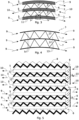
- the inter-turn spaces 6 comprise electrically insulating spacers and the inter-cable spaces 7 comprise electrically conductive spacers. These spacers have not been shown in the simplified view of the figure 2 and will be described below with reference to the Figures 3 to 5 .
- FIG 3 is an enlarged view of frame III visible at figure 2 .
- three portions of turns of conductor 3 therefore appear.
- a layer of insulation consisting of an electrically insulating spacer 8.
- a current flows from the first terminal of connection T1 to the second connection terminal T2 and arrows represent, on the figure 3 , the direction of passage of this current.
- the coil winding causes the formation of turns so that between a portion of the conductor 3 and another portion of the conductor 3 located on an adjacent turn, the current flows in the opposite direction.
- the flow of the current in one direction will be schematized by the arrows 9, while the flow of the current in the other direction (from right to left) will be schematized by arrows 10.
- the current flows from left to right according to arrows 9; on the middle portion of the turn, the current flows from right to left according to arrows 10; and on the bottom portion of the turn, the current flows from left to right according to arrows 9.
- the insulating spacer 8 has a shape adapted to maintain the inter-turn space 6, to electrically insulate the two corresponding adjacent turns, and to be permeable to a cooling fluid.
- the insulating spacer 8 is made of any insulating material sufficiently rigid to allow the spacing of the inter-turn space 6 to be maintained.
- the insulating spacer 8 is here made of a pleated sheet of insulating material, that is to say folded into a triangle, or corrugated, which provides gaps 11 allowing the passage of the cooling fluid.
- the current limiter 1 is cooled to the appropriate temperature for maintaining the superconducting properties of the conductor 3.
- the coil(s) 2 are thus bathed in a fluid such as liquid nitrogen, or this fluid is circulated by a cooling circuit.
- This cooling fluid is in contact with the conductor 3 thanks to the interstices 11 of the insulating spacers 8 and thanks to the interstices 13 of the conductive spacers 12.
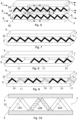
- FIG 4 is an enlargement of frame IV visible at figures 2 And 3 .
- This enlargement represents a portion of the conductor 3.
- the direction 9 of current flow is the same.
- Conductive spacers 12 are arranged between these cables 5, within the conductor 3, in the intercable spaces 7.
- the conductive spacers 12 have structurally the same shape, in the present example, as the insulating spacer 8 and have gaps 13 allowing the passage of the cooling fluid and the thermal exchanges directly with the cables 5 and indirectly via the conductive spacers 12.
- the conductive spacers 12 are made of an electrically conductive material, for example a metal or a semiconductor material.
- the conductive spacers 12 are each in contact with two cables 5 and thus ensure electrical continuity between these two cables 5.
- the cables 5 have superconducting properties while the conductive spacers 12 have the properties of a conventional conductor.
- the current will therefore preferably flow in the superconducting cables 5, which have almost zero resistance, rather than in the conductive spacers 12 which, although conductive, have a certain resistance.
- the conductive spacers 12 will however balance the distribution of the current as well as the potentials and ensure that a significant potential difference between two superconducting cables 5 of the same conductor 3 cannot develop.
- the cooling of the entire coil 2 is ensured by the same cooling fluid which passes both through the insulating spacers 8 and through the conductive spacers 12.
- the metal constituting the conductive spacers is preferably a metal having a high thermal conductivity, for example greater than 150 W/m/K, such as copper or aluminum. The thermal conductivity and electrical conductivity functions are thus optimally ensured by the conductive spacers 12.
- conductive spacer geometries 12 will be used which optimize the heat exchanges between the conductive spacers 12 and the cooling fluid, and which optimize the heat exchanges and the electrical conduction between two cables 5.
- finned structures can be used, as well as any method reducing the contact resistances.
- FIG. 5 schematically illustrates a portion of the coil 2 showing two adjacent turns of the conductor 3 and the arrangement of the insulating 8 and conductive 12 spacers.
- the interturn spaces 6 and the intercable spaces 7 have the same spacing.
- the insulating spacer 8 and the conductive spacers 12 here have the same shape, the same dimensions, and differ in their material of constitution, respectively insulating and electrically conductive. Alternatively, the sizes of spacers 8 and 12 may be different from each other if it is desired to achieve variable spacings between the cables 3 and/or between the conductors 5, within the coil.
- the superconducting cables 5 constituting the conductor 3 are conventional superconducting ribbons, for example REBCO type ribbons.
- the insulating spacer 8 and the conductive spacers 12 are pleated ribbons.
- FIG. 5 therefore represents: on the top of the figure, a first portion of the conductor 3, with the three portions of cables 5 constituting it; and on the bottom of the figure, a second portion of the conductor 3, corresponding to the adjacent turn, with the three portions of cables 5 constituting it.
- Two portions of conductive spacers 12 appear within each conductor 3, between the cables 5.
- a portion of insulating spacer 8 is visible between the two conductors 3, as well as above the portion of the conductor 3 on top, and below the portion of the conductor 3 on the bottom, for cooperation with the adjacent turns not shown.
- FIG. 6 represents a portion of the conductor 3 and shows the three cables 5A, 5B, 5C constituting it, as well as the two conductive spacers 12 maintaining the gap and the electrical conductivity between these three cables 5.
- the current flows in the direction of the arrows 9.
- This figure 6 illustrates the behavior of driver 3 in the event of the appearance of a hot spot 14.
- hot spot 14 appears on the middle cable 5B. Upstream of hot spot 14, the current flows in the same way in cables 5A, 5B, 5C, benefiting from their superconducting properties. On cable 5B, the current, upon reaching hot spot 14, no longer benefits from the superconducting properties of the cable, which can even become highly resistive locally.
- the conductive spacers 12 Upstream of the hot point 14, at least a portion of the current will be diverted by the conductive spacers 12 and will thus bypass the hot point 14 via the other cables 5A, 5C. Downstream of the hot point 14, the conductive spacers balance the currents by allowing a portion of the current to return to the cable 5B.
- FIG 7 is a simplified view showing a portion comprising two superconducting cables 5 of the same conductor 3 and the conductive spacer 12 arranged between these two cables 5.
- the figure 7 illustrates the production of the conductive spacers 12 described in figures 5 And 6 .
- the conductive spacer 12 of the figure 7 is therefore made up of a pleated metal ribbon in contact, on either side, with the two cables 5.
- the variant of the figure 8 illustrates a case where the conductive spacer 12 is discontinuous. It is formed of several discrete spacers 15 distributed over the entire length of the intercable space 7.
- the conductive spacer 12 therefore ensures electrical conduction between the two cables 5, in particular to balance the currents and bypass a possible hot spot.
- the conductive spacer 12 can only participate in the conduction of the current over certain portions of the length of the intercable space 7, which gives the conductive spacer 12 an anisotropic electrical conduction behavior, that is to say having a significant conductivity between two cables 5 but a low or even zero conductivity in the direction of flow of the current along the cables 5.
- This anisotropic conduction behavior prevents too great a reduction in the electrical resistance of coil 2 when it is in current limiting mode.
- FIG 9 illustrates another variant for the conductive spacer 12 providing it with anisotropic electrical conduction behavior.
- the conductive spacer 12 is made from an assembly of metal spacers 16 and insulating spacers 17 (shown hatched on the figure 17 ) arranged alternately along the intercable space 7.
- the conductive spacer 12 thus ensures spacing over the entire length of the intercable space 7 while limiting the flow of current along the conductive spacer 12 thanks to the insulating spacers 17, which are for example made of an electrically insulating polymer.
- FIG 10 illustrates a variant similar to the variant of the figure 9 , where the conductive spacer 12 is made up of an alternation of a conductive portion 12A (inverted V, in the figure) and an insulating portion 12B (inverted V).
- FIG 11 represents another variant where the alternation of the conductive and insulating portions is achieved by the fact that one 12A of the branches of the inverted V is conductive, and the other branch 12B is insulating.
- FIG 12 illustrates another variant for the production of the conductive spacer 12 also providing it with anisotropic electrical conduction behavior.
- the conductive spacer 12 is here produced by a succession of metal bridges 18 and crosspieces 19 arranged between these bridges 18.
- the metal bridges 18 provide electrical conductivity between the cables 5 and the crosspieces 19 hold the bridges 18 in position.
- the crosspieces 19 can be made of insulating material and the behavior of the conductive spacer 12 will then be similar to that of the variant of the figure 9
- the crosspieces 19 may also be made of conductive material, for example metal, the conductive spacer 12 then still exhibiting anisotropic behavior, preserving the conduction between the cables 5 while reducing it along the intercable space 7.
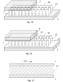
- FIG 13 illustrates an alternative arrangement of the crosspieces 19 in which the crosspieces 19 each connect two bridges 18, the upper crosspieces 19 being arranged in a staggered manner relative to the lower crosspieces 19.
- FIG 14 illustrates a variant where the bridges 18 are connected by soles 20 respectively to the upper cable 5 and to the lower cable 5.
- some 18 bridges are insulating (the insulating bridges 18 are shown hatched).
- FIGS 15 and 16 illustrate variants where the bridges 18 are made up of cylinders connecting the two cables 5.
- the bridges 18 directly connect the cables 5.
- the bridges 18 connect the cables 5 by means of a sole 20 arranged against each of the cables 5.
- the soles 20 of figures 14 And 16 furthermore increase the contact surface between the conductive spacer 12 and the cables 5 and thus promote heat exchange, which makes the cooling of the cables 5 by the cooling fluid more efficient.
- FIG 17 illustrates another embodiment in which the insulating spacer 12 is made of a material formed of conductive layers 12A and insulating layers 12B, alternately.
- THE figures 18 to 20 illustrate variations of the conductive spacer 12 relating to the heat exchange capacity of the conductive spacer 12.
- the conductive spacer 12 comprises bases 21 attaching the tops of the folds constituting the spacer 12 to the cables 5. These bases 21 increase the contact surface between the conductive spacer 12 and the cables 5 and thus promote heat exchange, which makes the cooling of the cables 5 by the cooling fluid more efficient.
- FIG 19 is similar to the figure 18 , the conductive spacer 12 being here corrugated.
- this corrugated shape of the spacer 12 can be provided without the bases 21.
- FIG 20 illustrates a variant of the conductive spacer 7, in which the spacer 12 comprises an additional heat exchanger consisting of fins 22 which increase the contact surface with the cooling fluid.
- the additional heat exchanger is here defined as a device for increasing the exchange surface of the spacer 12.
- FIG 21 illustrates an alternative embodiment of the coil 2 suitable for constituting a current limiter 1.
- the superconductor-type conductor 3 is arranged to make two round trips between the periphery of the coil and the center of the coil.
- conductive spacers are arranged in the intercable spaces 7 and insulating spacers are arranged in the interturn spaces 6.
- a superconductor conductor of the current limiter may comprise any number of superconductor cables to constitute it, one or more conductive spacers being arranged between these cables or groups of cables.
- a coil may comprise any number of superconducting conductors wound to form the coil and the corresponding number of connecting terminals, with one or more insulating spacers being provided to separate each turn formed by these different superconducting conductors.
- the coil can be any type of coil, bifilar or not. It can be cylindrical, oval, or rectangular in shape.
- the current limiter may also comprise any number of stacked coils, the connection terminals of which are connected together, in series or in parallel.
- the material and shape of the conductive spacers may vary while allowing both electrical conduction on at least portions of the conductive spacer, and permeability to the coolant.
- the conductive spacers may be made of a porous conductive material, or include coolant circulation conduits, for example.
- Anisotropic electrical conduction behavior can be provided to the electrically conductive spacers by other means such as through intrinsically anisotropic crystalline materials. These materials will be used to advantage by arranging them so that they have electrical conduction greater in the transverse direction, that is to say between two cables 3, than in the longitudinal direction, that is to say along the intercable spaces 7.
Landscapes
- Engineering & Computer Science (AREA)
- Power Engineering (AREA)
- Containers, Films, And Cooling For Superconductive Devices (AREA)
- Superconductors And Manufacturing Methods Therefor (AREA)
- Emergency Protection Circuit Devices (AREA)
Claims (18)
- Supraleitender Strombegrenzer (1), der mindestens einen supraleitenden Leiter (3) umfasst, der aufgewickelt ist, um eine Spule (2) zu bilden, die sich in einer einzigen Ebene erstreckt und eine erste elektrische Anschlussklemme (T1) mit einer zweiten elektrischen Anschlussklemme (T2) verbindet, wobei zwischen zwei Windungen der Spule (2) ein elektrisch isolierender Abstandshalter (8) angeordnet ist, dessen supraleitender Leiter (3) aus mindestens zwei separaten, parallel gewickelten supraleitenden Kabeln (5) gebildet ist, deren Enden jeweils durch die erste elektrische Anschlussklemme (T1) und die zweite elektrische Anschlussklemme (T2) elektrisch verbunden sind; und einen elektrisch leitenden Abstandshalter (12), der zwischen zwei der separaten supraleitenden Kabel (5) angeordnet ist, wobei dieser elektrisch leitende Abstandshalter (12) für ein Kühlfluid durchlässig ist, dadurch gekennzeichnet, dass der elektrisch leitende Abstandshalter (12) eine elektrische Kontinuität zwischen diesen beiden supraleitenden Kabeln (5) sicherstellt.
- Strombegrenzer nach Anspruch 1, dadurch gekennzeichnet, dass die Spule (2) eine zweiadrige Spule ist.
- Strombegrenzer nach einem der vorstehenden Ansprüche, dadurch gekennzeichnet, dass er einen Raum (6) zwischen zwei Windungen des supraleitenden Leiters (3) umfasst, und dass er einen Zwischenleitungsspalt (7) zwischen zwei supraleitenden Kabeln (5) desselben supraleitenden Leiters (3) umfasst, wobei der elektrisch isolierende Abstandshalter (8) entlang des Raums (6) zwischen Windungen angeordnet ist und der elektrisch leitende Abstandshalter (12) entlang des Raums (7) zwischen Kabel angeordnet ist.
- Strombegrenzer nach einem der vorstehenden Ansprüche, dadurch gekennzeichnet, dass der elektrisch leitende Abstandshalter (12) aus Metall besteht.
- Strombegrenzer nach einem der Ansprüche 1 bis 3, dadurch gekennzeichnet, dass der elektrisch leitende Abstandshalter (12) aus einem Halbleitermaterial besteht.
- Strombegrenzer nach Anspruch 5, dadurch gekennzeichnet, dass das Metall des elektrisch leitenden Abstandshalters (12) eine Wärmeleitfähigkeit größer als 150 W/m/K aufweist.
- Strombegrenzer nach einem der vorstehenden Ansprüche, dadurch gekennzeichnet, dass der elektrisch leitende Abstandshalter (12) die Form eines gefalteten oder gewellten Bandes aufweist.
- Strombegrenzer nach einem der vorstehenden Ansprüche, dadurch gekennzeichnet, dass der elektrisch leitende Abstandshalter (12) Durchgangslücken (13) für das Kühlfluid aufweist.
- Strombegrenzer nach einem der vorstehenden Ansprüche, dadurch gekennzeichnet, dass der elektrisch leitende Abstandshalter (12) und der elektrisch isolierende Abstandshalter (8) im Wesentlichen die gleiche Form aufweisen.
- Strombegrenzer nach einem der vorstehenden Ansprüche, dadurch gekennzeichnet, dass der elektrisch leitende Abstandshalter (12) ein anisotropes elektrisches Leitungsverhalten aufweist, das die elektrische Leitung zwischen den beiden supraleitenden Kabeln (5) fördert.
- Strombegrenzer nach Anspruch 10, dadurch gekennzeichnet, dass der elektrisch leitende Abstandshalter (12) diskontinuierlich ist und aus separaten Beabstandungselementen (15) gebildet ist.
- Strombegrenzer nach Anspruch 10, dadurch gekennzeichnet, dass der elektrisch leitende Abstandshalter (12) aus einer Nebeneinanderstellung leitenden Beabstandungselemente (16) und isolierenden Beabstandungselementen (17) gebildet ist.
- Strombegrenzer nach Anspruch 10, dadurch gekennzeichnet, dass der elektrisch leitende Abstandshalter (12) Metallbrücken (18) zwischen den beiden supraleitenden Kabeln (5) und Querstreben (19), die zwischen diesen Metallbrücken angeordnet sind, aufweist.
- Strombegrenzer nach Anspruch 13, dadurch gekennzeichnet, dass die Querstreben (19) elektrisch leitend sind.
- Strombegrenzer nach Anspruch 13, dadurch gekennzeichnet, dass die Querstreben (19) elektrisch isolierend sind.
- Strombegrenzer nach einem der vorstehenden Ansprüche, dadurch gekennzeichnet, dass er außerdem eine Kühlvorrichtung umfasst, die ein Kühlfluid umfasst, das mit den elektrisch isolierenden Abstandshaltern (8) zwischen den Windungen der Spule (2) und mit den elektrisch leitenden Abstandshaltern (9) zwischen den supraleitenden Kabeln (5) in Kontakt steht.
- Strombegrenzer nach einem der vorstehenden Ansprüche, dadurch gekennzeichnet, dass der leitende Abstandshalter (12) Sohlen (20) oder Sockel (21) aufweist, die die Kontaktoberfläche zu den beiden supraleitenden Kabeln (5) vergrößern.
- Strombegrenzer nach einem der vorstehenden Ansprüche, dadurch gekennzeichnet, dass der leitende Abstandshalter (12) zusätzliche Wärmetauscher (22) zum Wärmeaustausch mit dem Kühlfluid umfasst.
Applications Claiming Priority (2)
| Application Number | Priority Date | Filing Date | Title |
|---|---|---|---|
| FR1854132A FR3081259B1 (fr) | 2018-05-17 | 2018-05-17 | Limiteur de courant supraconducteur avec entretoise electriquement conductrice |
| PCT/EP2019/062660 WO2019219835A1 (fr) | 2018-05-17 | 2019-05-16 | Limiteur de courant supraconducteur avec entretoise électriquement conductrice |
Publications (3)
| Publication Number | Publication Date |
|---|---|
| EP3788656A1 EP3788656A1 (de) | 2021-03-10 |
| EP3788656C0 EP3788656C0 (de) | 2024-09-11 |
| EP3788656B1 true EP3788656B1 (de) | 2024-09-11 |
Family
ID=63963091
Family Applications (1)
| Application Number | Title | Priority Date | Filing Date |
|---|---|---|---|
| EP19725959.1A Active EP3788656B1 (de) | 2018-05-17 | 2019-05-16 | Supraleitender strombegrenzer mit elektrisch leitendem abstandshalter |
Country Status (7)
| Country | Link |
|---|---|
| US (1) | US11910729B2 (de) |
| EP (1) | EP3788656B1 (de) |
| KR (1) | KR102521412B1 (de) |
| CN (1) | CN112136222B (de) |
| FR (1) | FR3081259B1 (de) |
| RU (1) | RU2759833C1 (de) |
| WO (1) | WO2019219835A1 (de) |
Families Citing this family (2)
| Publication number | Priority date | Publication date | Assignee | Title |
|---|---|---|---|---|
| EP4026879A1 (de) | 2021-01-11 | 2022-07-13 | Hitachi Energy Switzerland AG | Abstandsband, verfahren zur herstellung einer wicklung sowie wicklung |
| KR102855070B1 (ko) * | 2024-08-16 | 2025-09-03 | 엘에스일렉트릭(주) | 초전도 코일 및 이의 권선 방법 |
Family Cites Families (16)
| Publication number | Priority date | Publication date | Assignee | Title |
|---|---|---|---|---|
| DE1489856A1 (de) * | 1965-11-13 | 1969-05-14 | Eder Dr Ing Franz X | Supraleitungsspule |
| US4189693A (en) * | 1977-12-28 | 1980-02-19 | The United States Of America As Represented By The United States Department Of Energy | Superconducting magnet |
| DE4107686A1 (de) | 1991-03-09 | 1992-09-10 | Abb Patent Gmbh | Verfahren zur herstellung eines supraleitenden strombegrenzers sowie ein entsprechend hergestellter strombegrenzer |
| US6275365B1 (en) | 1998-02-09 | 2001-08-14 | American Superconductor Corporation | Resistive fault current limiter |
| JP3892605B2 (ja) * | 1998-12-25 | 2007-03-14 | 株式会社東芝 | 限流素子用超電導コイル装置 |
| RU2204191C2 (ru) * | 2000-11-24 | 2003-05-10 | Марийский государственный технический университет | Комбинированный сверхпроводниковый ограничитель тока |
| DE102004048646B4 (de) * | 2004-10-04 | 2006-08-10 | Siemens Ag | Supraleitende Strombegrenzereinrichtung vom resistiven Typ mit bandförmiger Hoch-Tc-Supraleiterbahn |
| DE102006032702B3 (de) | 2006-07-14 | 2007-10-04 | Siemens Ag | Resistive supraleitende Strombegrenzeinrichtung mit bifilarer Spulenwicklung aus HTS-Bandleitern und Windungsabstandshalter |
| EP2117056B1 (de) * | 2008-03-05 | 2010-11-03 | Bruker HTS GmbH | Supraleitende Vorrichtung zur Stromkonditionierung |
| DE102008029722B3 (de) | 2008-06-23 | 2009-12-17 | Siemens Aktiengesellschaft | Leiteranordnung für ein resistives Schaltelement mit wenigstens zwei Leiterverbünden aus supraleitenden Leiterbändern |
| JP2010238943A (ja) * | 2009-03-31 | 2010-10-21 | Furukawa Electric Co Ltd:The | 限流器 |
| US8938278B2 (en) * | 2011-02-18 | 2015-01-20 | The Regents Of The University Of Colorado | Superconducting cables and methods of making the same |
| JP5305180B2 (ja) * | 2011-02-18 | 2013-10-02 | 住友電気工業株式会社 | 常温絶縁型超電導ケーブル、およびその製造方法 |
| RU2587680C1 (ru) * | 2015-04-07 | 2016-06-20 | Открытое Акционерное Общество "Федеральная Сетевая Компания Единой Энергетической Системы" (Оао "Фск Еэс") | Сверхпроводящий ограничитель тока |
| JPWO2017010326A1 (ja) * | 2015-07-16 | 2018-04-26 | 住友電気工業株式会社 | 超電導線材および限流器 |
| RU2691746C1 (ru) * | 2018-11-29 | 2019-06-18 | Закрытое акционерное общество "СуперОкс" (ЗАО "СуперОкс") | Токоограничивающее устройство на основе высокотемпературной сверхпроводимости |
-
2018
- 2018-05-17 FR FR1854132A patent/FR3081259B1/fr active Active
-
2019
- 2019-05-16 KR KR1020207036123A patent/KR102521412B1/ko active Active
- 2019-05-16 RU RU2020141149A patent/RU2759833C1/ru active
- 2019-05-16 CN CN201980032383.1A patent/CN112136222B/zh active Active
- 2019-05-16 US US17/055,929 patent/US11910729B2/en active Active
- 2019-05-16 WO PCT/EP2019/062660 patent/WO2019219835A1/fr not_active Ceased
- 2019-05-16 EP EP19725959.1A patent/EP3788656B1/de active Active
Also Published As
| Publication number | Publication date |
|---|---|
| CN112136222A (zh) | 2020-12-25 |
| KR20210018297A (ko) | 2021-02-17 |
| US11910729B2 (en) | 2024-02-20 |
| EP3788656C0 (de) | 2024-09-11 |
| FR3081259A1 (fr) | 2019-11-22 |
| KR102521412B1 (ko) | 2023-04-13 |
| FR3081259B1 (fr) | 2022-01-28 |
| EP3788656A1 (de) | 2021-03-10 |
| CN112136222B (zh) | 2024-07-05 |
| US20210184097A1 (en) | 2021-06-17 |
| RU2759833C1 (ru) | 2021-11-18 |
| WO2019219835A1 (fr) | 2019-11-21 |
Similar Documents
| Publication | Publication Date | Title |
|---|---|---|
| EP3788656B1 (de) | Supraleitender strombegrenzer mit elektrisch leitendem abstandshalter | |
| JP4810268B2 (ja) | 超電導線材の接続方法及び超電導線材 | |
| EP1671330B1 (de) | Magnettunnel-sperrschichtbauelement und schreib-/leseverfahren für das bauelement | |
| US11877521B2 (en) | Flexible multi-filament high temperature superconducting cable | |
| WO2017061563A1 (ja) | 超電導コイル | |
| JP3892605B2 (ja) | 限流素子用超電導コイル装置 | |
| JP2009212522A (ja) | 電流調整用超電導装置 | |
| WO2012041558A1 (fr) | Dispositif thermo électrique, notamment destiné à générer un courant électrique dans un véhicule automobile | |
| CA2282869C (fr) | Transformateur de courant electrique a bobinages supraconducteurs | |
| EP2567415B1 (de) | Modulierbare thermoelektrische vorrichtung | |
| FR2727555A1 (fr) | Tete magnetique d'enregistrement/lecture et son procede de realisation | |
| EP1580760B1 (de) | MRAM mit hoher Stromdichte | |
| EP3017486B1 (de) | Thermoelektrische vorrichtung, insbesondere zur erzeugung von elektrischem strom in einem kraftfahrzeug | |
| Ahn et al. | A study on the design of the stabilizer of coated conductor for applying to SFCL | |
| EP2591513B1 (de) | Vorrichtung zur erzeugung von strom und/oder spannung auf basis eines in einer fliessenden flüssigkeit platzierten thermoelektrischen moduls | |
| CA3124805A1 (fr) | Dispositif de recuperation d'energie sur au moins un conducteur de puissance et procede de fabrication dudit dispositif de recuperation | |
| JP4774494B2 (ja) | 超電導コイル | |
| EP3729478A1 (de) | Supraleitender strombegrenzender dipol mit mindestens vier supraleitenden kabeln | |
| EP0505975B1 (de) | Supraleiter mit verbessertem Schutz gegen partielle Übergänge | |
| FR2926686A1 (fr) | Stator de machine electrique tournante | |
| Lee et al. | Design of a high temperature superconducting coil for a 8.3 MVA fault current limiter | |
| JP4634954B2 (ja) | 超電導装置 | |
| WO2017046486A1 (fr) | Module et dispositif thermo électriques, notamment destinés a générer un courant électrique dans un véhicule automobile | |
| FR3076059A1 (fr) | Limiteur de courant a supraconducteur, avec couches d’isolant d’epaisseurs variables | |
| FR2644304A1 (fr) | Rotor de machine electrique avec enroulement d'excitation supraconducteur |
Legal Events
| Date | Code | Title | Description |
|---|---|---|---|
| STAA | Information on the status of an ep patent application or granted ep patent |
Free format text: STATUS: UNKNOWN |
|
| STAA | Information on the status of an ep patent application or granted ep patent |
Free format text: STATUS: THE INTERNATIONAL PUBLICATION HAS BEEN MADE |
|
| PUAI | Public reference made under article 153(3) epc to a published international application that has entered the european phase |
Free format text: ORIGINAL CODE: 0009012 |
|
| STAA | Information on the status of an ep patent application or granted ep patent |
Free format text: STATUS: REQUEST FOR EXAMINATION WAS MADE |
|
| 17P | Request for examination filed |
Effective date: 20201201 |
|
| AK | Designated contracting states |
Kind code of ref document: A1 Designated state(s): AL AT BE BG CH CY CZ DE DK EE ES FI FR GB GR HR HU IE IS IT LI LT LU LV MC MK MT NL NO PL PT RO RS SE SI SK SM TR |
|
| AX | Request for extension of the european patent |
Extension state: BA ME |
|
| DAV | Request for validation of the european patent (deleted) | ||
| DAX | Request for extension of the european patent (deleted) | ||
| REG | Reference to a national code |
Ref country code: DE Ref legal event code: R079 Free format text: PREVIOUS MAIN CLASS: H01L0039160000 Ipc: H10N0060300000 Ref document number: 602019058673 Country of ref document: DE |
|
| RIC1 | Information provided on ipc code assigned before grant |
Ipc: H10N 60/30 20230101AFI20240319BHEP |
|
| GRAP | Despatch of communication of intention to grant a patent |
Free format text: ORIGINAL CODE: EPIDOSNIGR1 |
|
| STAA | Information on the status of an ep patent application or granted ep patent |
Free format text: STATUS: GRANT OF PATENT IS INTENDED |
|
| INTG | Intention to grant announced |
Effective date: 20240502 |
|
| GRAS | Grant fee paid |
Free format text: ORIGINAL CODE: EPIDOSNIGR3 |
|
| GRAA | (expected) grant |
Free format text: ORIGINAL CODE: 0009210 |
|
| STAA | Information on the status of an ep patent application or granted ep patent |
Free format text: STATUS: THE PATENT HAS BEEN GRANTED |
|
| AK | Designated contracting states |
Kind code of ref document: B1 Designated state(s): AL AT BE BG CH CY CZ DE DK EE ES FI FR GB GR HR HU IE IS IT LI LT LU LV MC MK MT NL NO PL PT RO RS SE SI SK SM TR |
|
| REG | Reference to a national code |
Ref country code: GB Ref legal event code: FG4D Free format text: NOT ENGLISH |
|
| REG | Reference to a national code |
Ref country code: CH Ref legal event code: EP |
|
| REG | Reference to a national code |
Ref country code: DE Ref legal event code: R096 Ref document number: 602019058673 Country of ref document: DE |
|
| REG | Reference to a national code |
Ref country code: IE Ref legal event code: FG4D Free format text: LANGUAGE OF EP DOCUMENT: FRENCH |
|
| U01 | Request for unitary effect filed |
Effective date: 20241009 |
|
| U07 | Unitary effect registered |
Designated state(s): AT BE BG DE DK EE FI FR IT LT LU LV MT NL PT RO SE SI Effective date: 20241029 |
|
| PG25 | Lapsed in a contracting state [announced via postgrant information from national office to epo] |
Ref country code: NO Free format text: LAPSE BECAUSE OF FAILURE TO SUBMIT A TRANSLATION OF THE DESCRIPTION OR TO PAY THE FEE WITHIN THE PRESCRIBED TIME-LIMIT Effective date: 20241211 |
|
| PG25 | Lapsed in a contracting state [announced via postgrant information from national office to epo] |
Ref country code: GR Free format text: LAPSE BECAUSE OF FAILURE TO SUBMIT A TRANSLATION OF THE DESCRIPTION OR TO PAY THE FEE WITHIN THE PRESCRIBED TIME-LIMIT Effective date: 20241212 |
|
| PG25 | Lapsed in a contracting state [announced via postgrant information from national office to epo] |
Ref country code: HR Free format text: LAPSE BECAUSE OF FAILURE TO SUBMIT A TRANSLATION OF THE DESCRIPTION OR TO PAY THE FEE WITHIN THE PRESCRIBED TIME-LIMIT Effective date: 20240911 |
|
| PG25 | Lapsed in a contracting state [announced via postgrant information from national office to epo] |
Ref country code: RS Free format text: LAPSE BECAUSE OF FAILURE TO SUBMIT A TRANSLATION OF THE DESCRIPTION OR TO PAY THE FEE WITHIN THE PRESCRIBED TIME-LIMIT Effective date: 20241211 Ref country code: ES Free format text: LAPSE BECAUSE OF FAILURE TO SUBMIT A TRANSLATION OF THE DESCRIPTION OR TO PAY THE FEE WITHIN THE PRESCRIBED TIME-LIMIT Effective date: 20240911 |
|
| PG25 | Lapsed in a contracting state [announced via postgrant information from national office to epo] |
Ref country code: RS Free format text: LAPSE BECAUSE OF FAILURE TO SUBMIT A TRANSLATION OF THE DESCRIPTION OR TO PAY THE FEE WITHIN THE PRESCRIBED TIME-LIMIT Effective date: 20241211 Ref country code: NO Free format text: LAPSE BECAUSE OF FAILURE TO SUBMIT A TRANSLATION OF THE DESCRIPTION OR TO PAY THE FEE WITHIN THE PRESCRIBED TIME-LIMIT Effective date: 20241211 Ref country code: HR Free format text: LAPSE BECAUSE OF FAILURE TO SUBMIT A TRANSLATION OF THE DESCRIPTION OR TO PAY THE FEE WITHIN THE PRESCRIBED TIME-LIMIT Effective date: 20240911 Ref country code: GR Free format text: LAPSE BECAUSE OF FAILURE TO SUBMIT A TRANSLATION OF THE DESCRIPTION OR TO PAY THE FEE WITHIN THE PRESCRIBED TIME-LIMIT Effective date: 20241212 Ref country code: ES Free format text: LAPSE BECAUSE OF FAILURE TO SUBMIT A TRANSLATION OF THE DESCRIPTION OR TO PAY THE FEE WITHIN THE PRESCRIBED TIME-LIMIT Effective date: 20240911 |
|
| PG25 | Lapsed in a contracting state [announced via postgrant information from national office to epo] |
Ref country code: IS Free format text: LAPSE BECAUSE OF FAILURE TO SUBMIT A TRANSLATION OF THE DESCRIPTION OR TO PAY THE FEE WITHIN THE PRESCRIBED TIME-LIMIT Effective date: 20250111 |
|
| PG25 | Lapsed in a contracting state [announced via postgrant information from national office to epo] |
Ref country code: SM Free format text: LAPSE BECAUSE OF FAILURE TO SUBMIT A TRANSLATION OF THE DESCRIPTION OR TO PAY THE FEE WITHIN THE PRESCRIBED TIME-LIMIT Effective date: 20240911 |
|
| PG25 | Lapsed in a contracting state [announced via postgrant information from national office to epo] |
Ref country code: CZ Free format text: LAPSE BECAUSE OF FAILURE TO SUBMIT A TRANSLATION OF THE DESCRIPTION OR TO PAY THE FEE WITHIN THE PRESCRIBED TIME-LIMIT Effective date: 20240911 Ref country code: PL Free format text: LAPSE BECAUSE OF FAILURE TO SUBMIT A TRANSLATION OF THE DESCRIPTION OR TO PAY THE FEE WITHIN THE PRESCRIBED TIME-LIMIT Effective date: 20240911 |
|
| PG25 | Lapsed in a contracting state [announced via postgrant information from national office to epo] |
Ref country code: SK Free format text: LAPSE BECAUSE OF FAILURE TO SUBMIT A TRANSLATION OF THE DESCRIPTION OR TO PAY THE FEE WITHIN THE PRESCRIBED TIME-LIMIT Effective date: 20240911 |
|
| U20 | Renewal fee for the european patent with unitary effect paid |
Year of fee payment: 7 Effective date: 20250520 |
|
| PGFP | Annual fee paid to national office [announced via postgrant information from national office to epo] |
Ref country code: GB Payment date: 20250524 Year of fee payment: 7 |
|
| PLBE | No opposition filed within time limit |
Free format text: ORIGINAL CODE: 0009261 |
|
| STAA | Information on the status of an ep patent application or granted ep patent |
Free format text: STATUS: NO OPPOSITION FILED WITHIN TIME LIMIT |
|
| 26N | No opposition filed |
Effective date: 20250612 |
|
| REG | Reference to a national code |
Ref country code: CH Ref legal event code: H13 Free format text: ST27 STATUS EVENT CODE: U-0-0-H10-H13 (AS PROVIDED BY THE NATIONAL OFFICE) Effective date: 20251223 |
|
| PG25 | Lapsed in a contracting state [announced via postgrant information from national office to epo] |
Ref country code: CH Free format text: LAPSE BECAUSE OF NON-PAYMENT OF DUE FEES Effective date: 20250531 |
|
| PG25 | Lapsed in a contracting state [announced via postgrant information from national office to epo] |
Ref country code: MC Free format text: LAPSE BECAUSE OF FAILURE TO SUBMIT A TRANSLATION OF THE DESCRIPTION OR TO PAY THE FEE WITHIN THE PRESCRIBED TIME-LIMIT Effective date: 20240911 |
|
| PG25 | Lapsed in a contracting state [announced via postgrant information from national office to epo] |
Ref country code: IE Free format text: LAPSE BECAUSE OF NON-PAYMENT OF DUE FEES Effective date: 20250516 |