EP3787129B1 - Kontaktklemme mit mindestens einem impedanzsteuerungsmerkmal - Google Patents
Kontaktklemme mit mindestens einem impedanzsteuerungsmerkmal Download PDFInfo
- Publication number
- EP3787129B1 EP3787129B1 EP19193934.7A EP19193934A EP3787129B1 EP 3787129 B1 EP3787129 B1 EP 3787129B1 EP 19193934 A EP19193934 A EP 19193934A EP 3787129 B1 EP3787129 B1 EP 3787129B1
- Authority
- EP
- European Patent Office
- Prior art keywords
- contact
- terminal
- section
- impedance control
- contact element
- Prior art date
- Legal status (The legal status is an assumption and is not a legal conclusion. Google has not performed a legal analysis and makes no representation as to the accuracy of the status listed.)
- Active
Links
Images

Classifications
-
- H—ELECTRICITY
- H01—ELECTRIC ELEMENTS
- H01R—ELECTRICALLY-CONDUCTIVE CONNECTIONS; STRUCTURAL ASSOCIATIONS OF A PLURALITY OF MUTUALLY-INSULATED ELECTRICAL CONNECTING ELEMENTS; COUPLING DEVICES; CURRENT COLLECTORS
- H01R13/00—Details of coupling devices of the kinds covered by groups H01R12/70 or H01R24/00 - H01R33/00
- H01R13/648—Protective earth or shield arrangements on coupling devices, e.g. anti-static shielding
- H01R13/658—High frequency shielding arrangements, e.g. against EMI [Electro-Magnetic Interference] or EMP [Electro-Magnetic Pulse]
- H01R13/6591—Specific features or arrangements of connection of shield to conductive members
- H01R13/6592—Specific features or arrangements of connection of shield to conductive members the conductive member being a shielded cable
- H01R13/6593—Specific features or arrangements of connection of shield to conductive members the conductive member being a shielded cable the shield being composed of different pieces
-
- H—ELECTRICITY
- H01—ELECTRIC ELEMENTS
- H01R—ELECTRICALLY-CONDUCTIVE CONNECTIONS; STRUCTURAL ASSOCIATIONS OF A PLURALITY OF MUTUALLY-INSULATED ELECTRICAL CONNECTING ELEMENTS; COUPLING DEVICES; CURRENT COLLECTORS
- H01R13/00—Details of coupling devices of the kinds covered by groups H01R12/70 or H01R24/00 - H01R33/00
- H01R13/646—Details of coupling devices of the kinds covered by groups H01R12/70 or H01R24/00 - H01R33/00 specially adapted for high-frequency, e.g. structures providing an impedance match or phase match
- H01R13/6473—Impedance matching
-
- H—ELECTRICITY
- H01—ELECTRIC ELEMENTS
- H01R—ELECTRICALLY-CONDUCTIVE CONNECTIONS; STRUCTURAL ASSOCIATIONS OF A PLURALITY OF MUTUALLY-INSULATED ELECTRICAL CONNECTING ELEMENTS; COUPLING DEVICES; CURRENT COLLECTORS
- H01R13/00—Details of coupling devices of the kinds covered by groups H01R12/70 or H01R24/00 - H01R33/00
- H01R13/648—Protective earth or shield arrangements on coupling devices, e.g. anti-static shielding
- H01R13/658—High frequency shielding arrangements, e.g. against EMI [Electro-Magnetic Interference] or EMP [Electro-Magnetic Pulse]
- H01R13/6581—Shield structure
-
- H—ELECTRICITY
- H01—ELECTRIC ELEMENTS
- H01R—ELECTRICALLY-CONDUCTIVE CONNECTIONS; STRUCTURAL ASSOCIATIONS OF A PLURALITY OF MUTUALLY-INSULATED ELECTRICAL CONNECTING ELEMENTS; COUPLING DEVICES; CURRENT COLLECTORS
- H01R13/00—Details of coupling devices of the kinds covered by groups H01R12/70 or H01R24/00 - H01R33/00
- H01R13/40—Securing contact members in or to a base or case; Insulating of contact members
- H01R13/405—Securing in non-demountable manner, e.g. moulding, riveting
- H01R13/41—Securing in non-demountable manner, e.g. moulding, riveting by frictional grip in grommet, panel or base
-
- H—ELECTRICITY
- H01—ELECTRIC ELEMENTS
- H01R—ELECTRICALLY-CONDUCTIVE CONNECTIONS; STRUCTURAL ASSOCIATIONS OF A PLURALITY OF MUTUALLY-INSULATED ELECTRICAL CONNECTING ELEMENTS; COUPLING DEVICES; CURRENT COLLECTORS
- H01R13/00—Details of coupling devices of the kinds covered by groups H01R12/70 or H01R24/00 - H01R33/00
- H01R13/646—Details of coupling devices of the kinds covered by groups H01R12/70 or H01R24/00 - H01R33/00 specially adapted for high-frequency, e.g. structures providing an impedance match or phase match
- H01R13/6473—Impedance matching
- H01R13/6474—Impedance matching by variation of conductive properties, e.g. by dimension variations
-
- H—ELECTRICITY
- H01—ELECTRIC ELEMENTS
- H01R—ELECTRICALLY-CONDUCTIVE CONNECTIONS; STRUCTURAL ASSOCIATIONS OF A PLURALITY OF MUTUALLY-INSULATED ELECTRICAL CONNECTING ELEMENTS; COUPLING DEVICES; CURRENT COLLECTORS
- H01R13/00—Details of coupling devices of the kinds covered by groups H01R12/70 or H01R24/00 - H01R33/00
- H01R13/646—Details of coupling devices of the kinds covered by groups H01R12/70 or H01R24/00 - H01R33/00 specially adapted for high-frequency, e.g. structures providing an impedance match or phase match
- H01R13/6473—Impedance matching
- H01R13/6477—Impedance matching by variation of dielectric properties
-
- H—ELECTRICITY
- H01—ELECTRIC ELEMENTS
- H01R—ELECTRICALLY-CONDUCTIVE CONNECTIONS; STRUCTURAL ASSOCIATIONS OF A PLURALITY OF MUTUALLY-INSULATED ELECTRICAL CONNECTING ELEMENTS; COUPLING DEVICES; CURRENT COLLECTORS
- H01R2103/00—Two poles
Definitions
- the present invention relates to a contact terminal and, more particularly, to a shielded contact terminal for high-frequency data transmission.
- a transmission line it is preferable to match the impedance of a transmission line to the impedance of the load.
- a predefined, desired value may be the impedance of the load.
- the impedance control features may jointly compensate for the influence of the discontinuity on the impedance of the at least one contact element. Therefore, the signal integrity of the transmitted signal is substantially improved.
- each of the following optional features is advantageous on its own, and may be combined independently with any other optional feature.
- all impedance control features may be in the vicinity of and/or locally limited to the area of influence of the discontinuity, thus concentrating and maximizing the effect of the impedance control feature.
- the terminal shield may be a metal terminal shield.
- the metal terminal shield may be formed by bending a metal sheet circumferentially around the contact carrier, which represents a simple and reliable structure.
- the terminal shield may be a metal terminal shield enclosing the contact carrier and the at least one contact element along its entire length. This provides a protection for the contact carrier and the at least one contact element against electromagnetic effects, further improving signal integrity.
- the terminal shield and the contact carrier may engage in a form-fit connection and the discontinuity of the terminal shield may be part of the form-fit connection.
- the terminal shield may comprise at least one forward end at which the terminal shield is open for receiving a mating connector along an insertion direction.
- the discontinuity of the terminal shield may comprise or be a locking element formed in the outer circumference of the terminal shield, and the at least one impedance control feature may be aligned with said locking element.
- the locking element may be configured to interact with a suitable receptacle in order to fixate the terminal shield within the receptacle. This increases the applicability of the present invention due to the broader compatibility with the corresponding components deriving from the locking element.
- the locking element may be a locking groove extending at least partly along the outer circumference of the terminal shield.
- the locking groove may extend radially inwards toward the contact carrier and provide a seat for a complementary locking element e.g. of a suitable receptacle.
- the locking groove represents an embodiment that can easily be manufactured by bending or pressing. Thus, manufacturing is facilitated.
- the at least one impedance control feature may comprise or be an adjusted cross-section of the at least one contact element.
- the at least one contact element may extend longitudinally through the terminal shield along the insertion direction, and comprise an impedance control portion with an adjusted cross-section in the direct vicinity of the discontinuity of the terminal shield.
- the cross-sectional adjustment is an impedance control feature that allows simultaneous adjustment of at least two impedance-influencing factors, namely the cross-sectional area of the electrical conductor and the distance between the surfaces of the electrical conductor and neighboring conductors.
- the impedance control feature may comprise or be a section with a reduced cross-section. This could be the case, for example, in areas where the discontinuity of the terminal shield results in a narrowed inner diameter in comparison to the rest of the terminal shield.
- the terminal shield may comprise a section with a reduced cross-section.
- the at least one contact element also comprises a cross-section reduction. The cross-section reduction may be realized by a one-sidedly or two-sidedly decreased width of the at least one contact element.
- the at least one contact element may comprise a bonding portion on at least one other end, opposite the contact portion.
- the bonding portion may be configured for connecting it to an electrical conductor of a cable.
- the bonding portion may be connected, e.g. welded or soldered, to the electrical conductor of the cable.
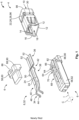
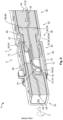
- the terminal shield 4 is a bent metal sheet 10, preferably comprising at least four shield walls 12 arranged in a circumferential direction C around a lead through-opening 14 extending along an insertion direction I. At at least one forward end 16, the terminal shield 4 may comprise an opening 18 at which the terminal shield 4 may receive a mating connector 20 inserted along the insertion direction I, as shown in Fig. 8 .
- the terminal shield 4 may be a metal shield made of a woven material.
- the terminal shield 4 may further have a discontinuity 22 in its design that affects the impedance of the pair of contact elements 8.
- multiple impedance control features 24 may be implemented on the contact carrier 6 and/or the pair of contact elements 8.
- the contact carrier 6 and each of the pair of contact elements 8 may possess at least one impedance control feature 24, and all impedance control features 24 may be aligned with the discontinuity 22 of the terminal shield 4 or at least be positioned in immediate proximity thereto. This is shown in Figs. 1 , 4 and 5 , and will be described in detail further below.
- the discontinuity 22 may be a locking element 26, preferably a locking groove 28 formed integrally by the terminal shield, extending along the outer circumference 30 of the terminal shield 4 and radially inwards toward the contact carrier 6.
- the terminal shield 4 may have a reduced outer traverse cross-section and a reduced inner traverse cross-section at the locking groove 28. The difference in the traverse cross-section between the locking groove 28 and the rest of the terminal shield 4 is covered by the terminal shield 4.
- the locking groove 28 may provide a seat for a complementary locking element (not shown), e.g. of a suitable receptacle (not shown).
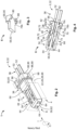
- the pair of contact elements 8 may be a pair of electrically conductive spring beams 32, which flatly extend in the insertion direction I.
- the pair of spring beams 32 may be formed mirror-invertedly to each other and positioned spaced apart from each other.
- Each of the spring beams 32 may comprise a contact portion 34 on one end, a bonding portion 36 on the opposite end and an impedance control portion 38 in between the contact portion 34 and the bonding portion 36.
- Each spring beam 32 may further comprise a transition portion 40 between the contact portion 34 and the impedance control portion 38 and a retention portion 42 between the impedance control portion 38 and the bonding portion 36.
- the cross-sectional area of the spring beam 32 needs to be reduced at the impedance control portion 38 in order to adjust the impedance of the spring beam 32 (the principles of the impedance control features have already been established in the above description of the present invention and will be omitted in this part).
- the retention portion 42 may be positioned adjacent to the impedance control portion 38 and comprise a retention tab 50 protruding sideways in a direction perpendicular to the insertion direction I.
- the retention tab 50 may be a plate-shaped part formed integrally by the material of the corresponding spring beam 32.
- the bonding portion 36 may be positioned adjacent to the retention portion 42 and comprise a bonding tab 52 protruding in the insertion direction I as a continuation of the spring beam 32.
- the bonding tab 52 may be a plate-shaped part formed integrally by the material of the corresponding spring beam 32.
- the bonding tab 52 has a width equal to the impedance control portion 38 and is configured for bonding with an electrical conductor 54 of a cable 56, as is shown in Fig. 8 .
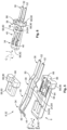
- the contact carrier 6 is made of an insulation material, which at least partially encloses the pair of contact elements 8.
- both contact elements 8 of the pair of contact elements 8 are enclosed by the same contact carrier 6.
- the contact carrier 6 encloses the pair of contact elements 8 at the impedance control portion 38 and at the surrounding of the impedance control portion 38.
- the contact carrier 6 may comprise at least two pieces 58 that are connected to each other to form the contact carrier 6.
- one of the two pieces 58 is opaque and contains no color pigment.
- the other of the two pieces 58 contains color pigment, preferably black and/or dark color pigment, so that the two pieces 58 may be connected through laser welding.
- each retaining groove 64 has a width larger than the impedance control portion of one of the pair of contact elements 8. This creates multiple air-filled gaps 72 between the inner surfaces 74 of the pair of retaining grooves 64 and the lateral surfaces 76 of each of the pair of contact elements 8. These air-filled gaps 72 represent further impedance control features 24.
- the spring beams 32 and/or the contact carrier 6 each may comprise lateral recesses 84, which are aligned with the discontinuity 22.
- These lateral recesses 84 represent impedance control features 24, which can be implemented in addition or as an alternative to the above mentioned impedance control features 24.
- the lateral recesses 84 are substantially trapezoidal cut-outs extending through the material of the spring beams 32 and/or contact carrier 6 in a direction perpendicular to the insertion direction I.
- the cut-outs in the contact carrier 6 may at least partially expose the impedance control portion 38 of the spring beams 32. It will be appreciated by those skilled in the art that the cut-outs may also have a cuboid or round shape.
Landscapes
- Details Of Connecting Devices For Male And Female Coupling (AREA)
- Coupling Device And Connection With Printed Circuit (AREA)
Claims (13)
- Kontaktklemme (1) mit einer Anschluss-Schirmung (4), einem Kontaktträger (6) und mindestens einem Kontaktelement (8) zur Führung elektrischer Signale einer hochfrequenten Datenübertragung, wobeider Kontaktträger (6) das mindestens eine Kontaktelement (8) in einer festen Position innerhalb der Anschluss-Schirmung (4) hält;die Anschluss-Schirmung (4) eine Unterbrechung (22) aufweist, die die Impedanz des mindestens einen Kontaktelements (8) beeinflusst; undder Kontaktträger (6) und das mindestens eine Kontaktelement (8) jeweils mindestens ein Impedanzsteuerungsmerkmal (24) aufweisen, das dazu ausgelegt ist, die Impedanz des mindestens einen Kontaktelements (8) entsprechend der Frequenz der Datenübertragung auf einen vordefinierten Sollwert einzustellen, dadurch gekennzeichnet, dass alle Impedanzsteuerungsmerkmale (24) auf die Unterbrechung (22) ausgerichtet sind und jedes der Impedanzsteuerungsmerkmale (24) ein Element einer Gruppe ist, die umfasst:- eine seitliche Aussparung (84) am Kontaktträger (6),- eine seitliche Aussparung (84) am mindestens einen Kontaktelement (8), und- mindestens einen Spalt (72), der das mindestens eine Kontaktelement (8) zumindest teilweise vom direkten Kontakt mit dem Kontaktträger (6) trennt.
- Kontaktklemme (1) nach Anspruch 1, wobeidie Unterbrechung (22) der Anschluss-Schirmung (4) ein im Außenumfang (30) der Anschluss-Schirmung (4) ausgebildetes Verriegelungselement (26) aufweist; unddas mindestens eine Impedanzsteuerungsmerkmal (24) mit dem Verriegelungselement (26) fluchtet.
- Kontaktklemme (1) nach Anspruch 2, wobei
das Verriegelungselement (26) eine Verriegelungsnut (28) ist, die sich zumindest teilweise entlang des Außenumfangs (30) der Anschluss-Schirmung (4) erstreckt. - Kontaktklemme (1) nach einem der Ansprüche 1 bis 3, wobei
das mindestens eine Impedanzsteuerungsmerkmal (24) einen angepassten Querschnitt des mindestens einen Kontaktelements (8) an einem Impedanzsteuerungsabschnitt (38) aufweist. - Kontaktklemme (1) nach Anspruch 4, wobei
das mindestens eine Kontaktelement (8) einen Übergangsabschnitt (40) mit einem Querschnitt aufweist, der größer ist als der Querschnitt des Impedanzsteuerungsabschnitts (38). - Kontaktklemme (1) nach einem der Ansprüche 1 bis 5, wobei
das mindestens eine Kontaktelement (8) einen Rückhalteabschnitt (42) mit mindestens einer seitlich vorstehenden Rückhaltefahne (50) aufweist. - Kontaktklemme (1) nach einem der Ansprüche 1 bis 6, wobeidie Kontaktklemme (1) ein Paar Kontaktelemente (8) aufweist, die beabstandet und elektrisch voneinander isoliert angeordnet sind; undjedes Kontaktelement (8) so konfiguriert ist, dass es ein Signal eines Differenzpaares von Signalen für eine Hochfrequenzdatenübertragung überträgt.
- Kontaktklemme (1) nach einem der Ansprüche 1 bis 7, wobeider Kontaktträger (6) aus einem Isolationsmaterial hergestellt ist, das das mindestens eine Kontaktelement (8) zumindest teilweise umschließt; unddas mindestens eine Impedanzsteuerungsmerkmal (24) eine angepasste Materialdicke des Kontaktträgers (6) aufweist.
- Kontaktklemme (1) nach einem der Ansprüche 1 bis 8, wobei
die Anschluss-Schirmung (4) einen Abschnitt (96) mit einem reduzierten Querschnitt aufweist; und das mindestens eine Kontaktelement (8) eine Querschnittsverringerung aufweist. - Kontaktklemme (1) nach einem der Ansprüche 1 bis 9, wobei
die Anschluss-Schirmung (4) einen Abschnitt (98) mit vergrößertem Querschnitt aufweist; und das mindestens eine Kontaktelement (8) eine Querschnittsvergrößerung aufweist. - Kontaktklemme (1) nach einem der Ansprüche 9 oder 10, wobei
die Querschnittsverringerung den Abschnitt (96) und/oder die Querschnittserhöhung den Abschnitt (98) in einer Richtung senkrecht zu einer Einsteckrichtung (I) überlappt. - Kontaktklemme (1) nach Anspruch 9 oder 10, wobei das mindestens eine Impedanzsteuerungsmerkmal mindestens eines einer einseitig verringerten Breite des mindestens einen Kontaktelements (8), einer beidseitig verringerten Breite des mindestens einen Kontaktelements (8), einer einseitig vergrößerten Breite des mindestens einen Kontaktelements (8) und einer beidseitig vergrößerten Breite des mindestens einen Kontaktelements (8) ist.
- Kontaktklemme (1) nach einem der Ansprüche 1 bis 12, wobei
die Anschluss-Schirmung (4) und der Kontaktträger (6) in eine Formschlussverbindung eingreifen; und die Unterbrechung (22) der Anschluss-Schirmung (4) Teil der Formschlussverbindung ist.
Priority Applications (5)
| Application Number | Priority Date | Filing Date | Title |
|---|---|---|---|
| EP19193934.7A EP3787129B1 (de) | 2019-08-27 | 2019-08-27 | Kontaktklemme mit mindestens einem impedanzsteuerungsmerkmal |
| JP2020139032A JP7665934B2 (ja) | 2019-08-27 | 2020-08-20 | 少なくとも1つのインピーダンス制御機構を有するコンタクト端子 |
| KR1020200106929A KR102839407B1 (ko) | 2019-08-27 | 2020-08-25 | 적어도 하나의 임피던스 제어 특징부를 갖는 접점 단자 |
| US17/002,256 US11283220B2 (en) | 2019-08-27 | 2020-08-25 | Contact terminal with at least one impedance control feature |
| CN202010868482.8A CN112448236B (zh) | 2019-08-27 | 2020-08-26 | 具有至少一个阻抗控制特征的触头端子 |
Applications Claiming Priority (1)
| Application Number | Priority Date | Filing Date | Title |
|---|---|---|---|
| EP19193934.7A EP3787129B1 (de) | 2019-08-27 | 2019-08-27 | Kontaktklemme mit mindestens einem impedanzsteuerungsmerkmal |
Publications (2)
| Publication Number | Publication Date |
|---|---|
| EP3787129A1 EP3787129A1 (de) | 2021-03-03 |
| EP3787129B1 true EP3787129B1 (de) | 2025-07-02 |
Family
ID=67777105
Family Applications (1)
| Application Number | Title | Priority Date | Filing Date |
|---|---|---|---|
| EP19193934.7A Active EP3787129B1 (de) | 2019-08-27 | 2019-08-27 | Kontaktklemme mit mindestens einem impedanzsteuerungsmerkmal |
Country Status (5)
| Country | Link |
|---|---|
| US (1) | US11283220B2 (de) |
| EP (1) | EP3787129B1 (de) |
| JP (1) | JP7665934B2 (de) |
| KR (1) | KR102839407B1 (de) |
| CN (1) | CN112448236B (de) |
Families Citing this family (1)
| Publication number | Priority date | Publication date | Assignee | Title |
|---|---|---|---|---|
| CN115101986B (zh) * | 2022-07-22 | 2022-11-25 | 深圳市众智动力科技有限公司 | 一种新能源汽车用以太网连接器外导体 |
Family Cites Families (18)
| Publication number | Priority date | Publication date | Assignee | Title |
|---|---|---|---|---|
| US5713764A (en) * | 1992-03-16 | 1998-02-03 | Molex Incorporated | Impedance and inductance control in electrical connectors |
| US6015315A (en) * | 1998-11-16 | 2000-01-18 | Itt Manufacturing Enterprises, Inc. | Impedance improved coax connector |
| WO2001006602A1 (en) | 1999-07-16 | 2001-01-25 | Molex Incorporated | Impedance-tuned connector |
| US6280209B1 (en) * | 1999-07-16 | 2001-08-28 | Molex Incorporated | Connector with improved performance characteristics |
| US6454605B1 (en) * | 1999-07-16 | 2002-09-24 | Molex Incorporated | Impedance-tuned termination assembly and connectors incorporating same |
| US7270573B2 (en) * | 2002-08-30 | 2007-09-18 | Fci Americas Technology, Inc. | Electrical connector with load bearing features |
| JP2005317260A (ja) * | 2004-04-27 | 2005-11-10 | Tyco Electronics Amp Kk | 同軸コネクタ |
| JP4549277B2 (ja) * | 2005-10-27 | 2010-09-22 | 矢崎総業株式会社 | コネクタ |
| US7731528B2 (en) | 2006-01-31 | 2010-06-08 | 3M Innovative Properties Company | Electrical termination device |
| US7387531B2 (en) * | 2006-08-16 | 2008-06-17 | Commscope, Inc. Of North Carolina | Universal coaxial connector |
| DE102009016227B4 (de) * | 2009-04-03 | 2017-12-28 | Kostal Kontakt Systeme Gmbh | Steckverbinder mit einem angebundenen Koaxialkabel |
| CN102044801B (zh) * | 2009-10-19 | 2013-05-08 | 富士康(昆山)电脑接插件有限公司 | 电连接器及其组装方法 |
| JP5768760B2 (ja) * | 2012-05-08 | 2015-08-26 | 日立金属株式会社 | 接続構造 |
| CN107017489B (zh) * | 2016-01-28 | 2019-09-06 | 莫列斯有限公司 | 电连接器 |
| JP2018067496A (ja) * | 2016-10-21 | 2018-04-26 | 住友電装株式会社 | シールド端子及び外導体端子 |
| JP6673267B2 (ja) | 2017-03-08 | 2020-03-25 | 株式会社オートネットワーク技術研究所 | シールド端子 |
| JP6642490B2 (ja) | 2017-03-08 | 2020-02-05 | 株式会社オートネットワーク技術研究所 | シールド端子 |
| DE102017105682A1 (de) | 2017-03-16 | 2018-09-20 | Te Connectivity Germany Gmbh | Kontaktträger, elektrische Kontakteinrichtung sowie Verfahren zum Herstellen eines konfektionierten Kabels |
-
2019
- 2019-08-27 EP EP19193934.7A patent/EP3787129B1/de active Active
-
2020
- 2020-08-20 JP JP2020139032A patent/JP7665934B2/ja active Active
- 2020-08-25 US US17/002,256 patent/US11283220B2/en active Active
- 2020-08-25 KR KR1020200106929A patent/KR102839407B1/ko active Active
- 2020-08-26 CN CN202010868482.8A patent/CN112448236B/zh active Active
Also Published As
| Publication number | Publication date |
|---|---|
| US20210066855A1 (en) | 2021-03-04 |
| JP2021034378A (ja) | 2021-03-01 |
| KR20210025493A (ko) | 2021-03-09 |
| KR102839407B1 (ko) | 2025-07-25 |
| JP7665934B2 (ja) | 2025-04-22 |
| CN112448236B (zh) | 2026-02-06 |
| EP3787129A1 (de) | 2021-03-03 |
| CN112448236A (zh) | 2021-03-05 |
| US11283220B2 (en) | 2022-03-22 |
Similar Documents
| Publication | Publication Date | Title |
|---|---|---|
| JP3564556B2 (ja) | コネクタ | |
| EP3584891B1 (de) | Schirmanschluss und schildkabelanordnung mit klemme | |
| EP2174386B1 (de) | Koaxialkabelstecker mit ausgleichslasche | |
| KR20170081202A (ko) | 커넥터 | |
| JP2025081755A (ja) | 少なくとも1つのインピーダンス制御構造を有するカバーアセンブリ | |
| US10468837B2 (en) | Coaxial connector assembly | |
| US11075488B2 (en) | Impedance control connector with dielectric seperator rib | |
| KR102808068B1 (ko) | 임피던스 제어 커넥터 | |
| WO2021059970A1 (ja) | 電気コネクタおよび電気コネクタセット | |
| KR101085707B1 (ko) | 개선된 차폐성을 갖는 동축 케이블 커넥터 | |
| JP6763418B2 (ja) | 電気コネクタ | |
| EP3787129B1 (de) | Kontaktklemme mit mindestens einem impedanzsteuerungsmerkmal | |
| US11317547B2 (en) | Shielding housing for a detachable fully shielded internal cable assembly | |
| EP4136713A1 (de) | Kabelanordnung mit dielektrischem klappverbinder zur impedanzsteuerung | |
| CN214254971U (zh) | 一种低信号对外辐射的高频连接器 | |
| US8961223B2 (en) | F-connector with chamfered lock ring | |
| CN118017302A (zh) | 连接器装置 | |
| KR20230069854A (ko) | 동축 플러그를 위한 접촉 배열체 및 다중 접촉 배열체 | |
| US11626701B2 (en) | Coaxial connector having inclined surface on tip end side of shell | |
| US20250233364A1 (en) | Electrical connector, cable, and connection assembly |
Legal Events
| Date | Code | Title | Description |
|---|---|---|---|
| PUAI | Public reference made under article 153(3) epc to a published international application that has entered the european phase |
Free format text: ORIGINAL CODE: 0009012 |
|
| STAA | Information on the status of an ep patent application or granted ep patent |
Free format text: STATUS: THE APPLICATION HAS BEEN PUBLISHED |
|
| AK | Designated contracting states |
Kind code of ref document: A1 Designated state(s): AL AT BE BG CH CY CZ DE DK EE ES FI FR GB GR HR HU IE IS IT LI LT LU LV MC MK MT NL NO PL PT RO RS SE SI SK SM TR |
|
| AX | Request for extension of the european patent |
Extension state: BA ME |
|
| STAA | Information on the status of an ep patent application or granted ep patent |
Free format text: STATUS: REQUEST FOR EXAMINATION WAS MADE |
|
| 17P | Request for examination filed |
Effective date: 20210903 |
|
| RBV | Designated contracting states (corrected) |
Designated state(s): AL AT BE BG CH CY CZ DE DK EE ES FI FR GB GR HR HU IE IS IT LI LT LU LV MC MK MT NL NO PL PT RO RS SE SI SK SM TR |
|
| STAA | Information on the status of an ep patent application or granted ep patent |
Free format text: STATUS: EXAMINATION IS IN PROGRESS |
|
| 17Q | First examination report despatched |
Effective date: 20230223 |
|
| GRAP | Despatch of communication of intention to grant a patent |
Free format text: ORIGINAL CODE: EPIDOSNIGR1 |
|
| STAA | Information on the status of an ep patent application or granted ep patent |
Free format text: STATUS: GRANT OF PATENT IS INTENDED |
|
| RIC1 | Information provided on ipc code assigned before grant |
Ipc: H01R 13/6474 20110101ALN20250211BHEP Ipc: H01R 13/41 20060101ALN20250211BHEP Ipc: H01R 103/00 20060101ALN20250211BHEP Ipc: H01R 13/6473 20110101ALI20250211BHEP Ipc: H01R 13/6477 20110101AFI20250211BHEP |
|
| INTG | Intention to grant announced |
Effective date: 20250311 |
|
| GRAS | Grant fee paid |
Free format text: ORIGINAL CODE: EPIDOSNIGR3 |
|
| GRAA | (expected) grant |
Free format text: ORIGINAL CODE: 0009210 |
|
| STAA | Information on the status of an ep patent application or granted ep patent |
Free format text: STATUS: THE PATENT HAS BEEN GRANTED |
|
| AK | Designated contracting states |
Kind code of ref document: B1 Designated state(s): AL AT BE BG CH CY CZ DE DK EE ES FI FR GB GR HR HU IE IS IT LI LT LU LV MC MK MT NL NO PL PT RO RS SE SI SK SM TR |
|
| REG | Reference to a national code |
Ref country code: GB Ref legal event code: FG4D |
|
| REG | Reference to a national code |
Ref country code: CH Ref legal event code: EP |
|
| REG | Reference to a national code |
Ref country code: DE Ref legal event code: R096 Ref document number: 602019071860 Country of ref document: DE |
|
| REG | Reference to a national code |
Ref country code: IE Ref legal event code: FG4D |
|
| PGFP | Annual fee paid to national office [announced via postgrant information from national office to epo] |
Ref country code: DE Payment date: 20250702 Year of fee payment: 7 |
|
| PGFP | Annual fee paid to national office [announced via postgrant information from national office to epo] |
Ref country code: IT Payment date: 20250925 Year of fee payment: 7 |
|
| PGFP | Annual fee paid to national office [announced via postgrant information from national office to epo] |
Ref country code: FR Payment date: 20250703 Year of fee payment: 7 |
|
| REG | Reference to a national code |
Ref country code: NL Ref legal event code: MP Effective date: 20250702 |
|
| PG25 | Lapsed in a contracting state [announced via postgrant information from national office to epo] |
Ref country code: PT Free format text: LAPSE BECAUSE OF FAILURE TO SUBMIT A TRANSLATION OF THE DESCRIPTION OR TO PAY THE FEE WITHIN THE PRESCRIBED TIME-LIMIT Effective date: 20251103 |
|
| PG25 | Lapsed in a contracting state [announced via postgrant information from national office to epo] |
Ref country code: NL Free format text: LAPSE BECAUSE OF FAILURE TO SUBMIT A TRANSLATION OF THE DESCRIPTION OR TO PAY THE FEE WITHIN THE PRESCRIBED TIME-LIMIT Effective date: 20250702 |
|
| REG | Reference to a national code |
Ref country code: AT Ref legal event code: MK05 Ref document number: 1810373 Country of ref document: AT Kind code of ref document: T Effective date: 20250702 |
|
| PG25 | Lapsed in a contracting state [announced via postgrant information from national office to epo] |
Ref country code: IS Free format text: LAPSE BECAUSE OF FAILURE TO SUBMIT A TRANSLATION OF THE DESCRIPTION OR TO PAY THE FEE WITHIN THE PRESCRIBED TIME-LIMIT Effective date: 20251102 |
|
| PG25 | Lapsed in a contracting state [announced via postgrant information from national office to epo] |
Ref country code: NO Free format text: LAPSE BECAUSE OF FAILURE TO SUBMIT A TRANSLATION OF THE DESCRIPTION OR TO PAY THE FEE WITHIN THE PRESCRIBED TIME-LIMIT Effective date: 20251002 |
|
| REG | Reference to a national code |
Ref country code: LT Ref legal event code: MG9D |
|
| PG25 | Lapsed in a contracting state [announced via postgrant information from national office to epo] |
Ref country code: AT Free format text: LAPSE BECAUSE OF FAILURE TO SUBMIT A TRANSLATION OF THE DESCRIPTION OR TO PAY THE FEE WITHIN THE PRESCRIBED TIME-LIMIT Effective date: 20250702 |
|
| PG25 | Lapsed in a contracting state [announced via postgrant information from national office to epo] |
Ref country code: FI Free format text: LAPSE BECAUSE OF FAILURE TO SUBMIT A TRANSLATION OF THE DESCRIPTION OR TO PAY THE FEE WITHIN THE PRESCRIBED TIME-LIMIT Effective date: 20250702 |
|
| PG25 | Lapsed in a contracting state [announced via postgrant information from national office to epo] |
Ref country code: HR Free format text: LAPSE BECAUSE OF FAILURE TO SUBMIT A TRANSLATION OF THE DESCRIPTION OR TO PAY THE FEE WITHIN THE PRESCRIBED TIME-LIMIT Effective date: 20250702 |
|
| PG25 | Lapsed in a contracting state [announced via postgrant information from national office to epo] |
Ref country code: GR Free format text: LAPSE BECAUSE OF FAILURE TO SUBMIT A TRANSLATION OF THE DESCRIPTION OR TO PAY THE FEE WITHIN THE PRESCRIBED TIME-LIMIT Effective date: 20251003 |
|
| PG25 | Lapsed in a contracting state [announced via postgrant information from national office to epo] |
Ref country code: SE Free format text: LAPSE BECAUSE OF FAILURE TO SUBMIT A TRANSLATION OF THE DESCRIPTION OR TO PAY THE FEE WITHIN THE PRESCRIBED TIME-LIMIT Effective date: 20250702 Ref country code: CZ Free format text: LAPSE BECAUSE OF FAILURE TO SUBMIT A TRANSLATION OF THE DESCRIPTION OR TO PAY THE FEE WITHIN THE PRESCRIBED TIME-LIMIT Effective date: 20250702 |
|
| PG25 | Lapsed in a contracting state [announced via postgrant information from national office to epo] |
Ref country code: LV Free format text: LAPSE BECAUSE OF FAILURE TO SUBMIT A TRANSLATION OF THE DESCRIPTION OR TO PAY THE FEE WITHIN THE PRESCRIBED TIME-LIMIT Effective date: 20250702 |
|
| PG25 | Lapsed in a contracting state [announced via postgrant information from national office to epo] |
Ref country code: BG Free format text: LAPSE BECAUSE OF FAILURE TO SUBMIT A TRANSLATION OF THE DESCRIPTION OR TO PAY THE FEE WITHIN THE PRESCRIBED TIME-LIMIT Effective date: 20250702 Ref country code: PL Free format text: LAPSE BECAUSE OF FAILURE TO SUBMIT A TRANSLATION OF THE DESCRIPTION OR TO PAY THE FEE WITHIN THE PRESCRIBED TIME-LIMIT Effective date: 20250702 |
|
| PG25 | Lapsed in a contracting state [announced via postgrant information from national office to epo] |
Ref country code: RS Free format text: LAPSE BECAUSE OF FAILURE TO SUBMIT A TRANSLATION OF THE DESCRIPTION OR TO PAY THE FEE WITHIN THE PRESCRIBED TIME-LIMIT Effective date: 20251002 |
|
| PG25 | Lapsed in a contracting state [announced via postgrant information from national office to epo] |
Ref country code: ES Free format text: LAPSE BECAUSE OF FAILURE TO SUBMIT A TRANSLATION OF THE DESCRIPTION OR TO PAY THE FEE WITHIN THE PRESCRIBED TIME-LIMIT Effective date: 20250702 |