EP3780403B1 - Power wiring network device - Google Patents
Power wiring network device Download PDFInfo
- Publication number
- EP3780403B1 EP3780403B1 EP19776463.2A EP19776463A EP3780403B1 EP 3780403 B1 EP3780403 B1 EP 3780403B1 EP 19776463 A EP19776463 A EP 19776463A EP 3780403 B1 EP3780403 B1 EP 3780403B1
- Authority
- EP
- European Patent Office
- Prior art keywords
- connector
- power
- data
- energy harvesting
- signal
- Prior art date
- Legal status (The legal status is an assumption and is not a legal conclusion. Google has not performed a legal analysis and makes no representation as to the accuracy of the status listed.)
- Active
Links
- 238000003306 harvesting Methods 0.000 claims description 151
- 230000005540 biological transmission Effects 0.000 claims description 78
- 238000004891 communication Methods 0.000 claims description 57
- 230000002265 prevention Effects 0.000 claims description 41
- 230000002441 reversible effect Effects 0.000 claims description 41
- 238000007726 management method Methods 0.000 description 72
- 238000003860 storage Methods 0.000 description 17
- 238000005452 bending Methods 0.000 description 10
- 238000012545 processing Methods 0.000 description 10
- 239000004020 conductor Substances 0.000 description 8
- 238000010586 diagram Methods 0.000 description 8
- 238000009429 electrical wiring Methods 0.000 description 8
- 230000006870 function Effects 0.000 description 8
- 238000000034 method Methods 0.000 description 8
- 238000013500 data storage Methods 0.000 description 7
- 230000000670 limiting effect Effects 0.000 description 7
- 230000008859 change Effects 0.000 description 6
- 238000003780 insertion Methods 0.000 description 6
- 230000037431 insertion Effects 0.000 description 6
- 238000010248 power generation Methods 0.000 description 6
- 230000015654 memory Effects 0.000 description 5
- XEEYBQQBJWHFJM-UHFFFAOYSA-N Iron Chemical compound [Fe] XEEYBQQBJWHFJM-UHFFFAOYSA-N 0.000 description 4
- PXHVJJICTQNCMI-UHFFFAOYSA-N Nickel Chemical compound [Ni] PXHVJJICTQNCMI-UHFFFAOYSA-N 0.000 description 4
- 238000006243 chemical reaction Methods 0.000 description 4
- 230000007274 generation of a signal involved in cell-cell signaling Effects 0.000 description 4
- 239000007769 metal material Substances 0.000 description 4
- 230000003014 reinforcing effect Effects 0.000 description 4
- 150000001875 compounds Chemical class 0.000 description 3
- 238000013461 design Methods 0.000 description 3
- 238000006073 displacement reaction Methods 0.000 description 3
- 238000005259 measurement Methods 0.000 description 3
- 230000004048 modification Effects 0.000 description 3
- 238000012986 modification Methods 0.000 description 3
- 230000008569 process Effects 0.000 description 3
- RYGMFSIKBFXOCR-UHFFFAOYSA-N Copper Chemical compound [Cu] RYGMFSIKBFXOCR-UHFFFAOYSA-N 0.000 description 2
- XUIMIQQOPSSXEZ-UHFFFAOYSA-N Silicon Chemical compound [Si] XUIMIQQOPSSXEZ-UHFFFAOYSA-N 0.000 description 2
- BQCADISMDOOEFD-UHFFFAOYSA-N Silver Chemical compound [Ag] BQCADISMDOOEFD-UHFFFAOYSA-N 0.000 description 2
- GWEVSGVZZGPLCZ-UHFFFAOYSA-N Titan oxide Chemical compound O=[Ti]=O GWEVSGVZZGPLCZ-UHFFFAOYSA-N 0.000 description 2
- 239000000956 alloy Substances 0.000 description 2
- 229910052782 aluminium Inorganic materials 0.000 description 2
- XAGFODPZIPBFFR-UHFFFAOYSA-N aluminium Chemical compound [Al] XAGFODPZIPBFFR-UHFFFAOYSA-N 0.000 description 2
- 238000004458 analytical method Methods 0.000 description 2
- 238000003491 array Methods 0.000 description 2
- 239000000470 constituent Substances 0.000 description 2
- 238000010276 construction Methods 0.000 description 2
- 229910052802 copper Inorganic materials 0.000 description 2
- 239000010949 copper Substances 0.000 description 2
- 230000005611 electricity Effects 0.000 description 2
- PCHJSUWPFVWCPO-UHFFFAOYSA-N gold Chemical compound [Au] PCHJSUWPFVWCPO-UHFFFAOYSA-N 0.000 description 2
- 229910052737 gold Inorganic materials 0.000 description 2
- 239000010931 gold Substances 0.000 description 2
- 239000011810 insulating material Substances 0.000 description 2
- 229910052742 iron Inorganic materials 0.000 description 2
- 238000012544 monitoring process Methods 0.000 description 2
- 229910052759 nickel Inorganic materials 0.000 description 2
- 239000002985 plastic film Substances 0.000 description 2
- 229920006255 plastic film Polymers 0.000 description 2
- 230000002829 reductive effect Effects 0.000 description 2
- 230000008054 signal transmission Effects 0.000 description 2
- 229910052710 silicon Inorganic materials 0.000 description 2
- 239000010703 silicon Substances 0.000 description 2
- 229910052709 silver Inorganic materials 0.000 description 2
- 239000004332 silver Substances 0.000 description 2
- 230000007704 transition Effects 0.000 description 2
- 239000004593 Epoxy Substances 0.000 description 1
- HBBGRARXTFLTSG-UHFFFAOYSA-N Lithium ion Chemical compound [Li+] HBBGRARXTFLTSG-UHFFFAOYSA-N 0.000 description 1
- ISWSIDIOOBJBQZ-UHFFFAOYSA-N Phenol Chemical compound OC1=CC=CC=C1 ISWSIDIOOBJBQZ-UHFFFAOYSA-N 0.000 description 1
- 230000008901 benefit Effects 0.000 description 1
- 239000003990 capacitor Substances 0.000 description 1
- 229920001940 conductive polymer Polymers 0.000 description 1
- 230000003247 decreasing effect Effects 0.000 description 1
- 230000001419 dependent effect Effects 0.000 description 1
- 238000007599 discharging Methods 0.000 description 1
- 238000009826 distribution Methods 0.000 description 1
- 230000000694 effects Effects 0.000 description 1
- 239000003792 electrolyte Substances 0.000 description 1
- 239000004744 fabric Substances 0.000 description 1
- 239000011521 glass Substances 0.000 description 1
- 229910052739 hydrogen Inorganic materials 0.000 description 1
- 239000001257 hydrogen Substances 0.000 description 1
- 230000001771 impaired effect Effects 0.000 description 1
- 229910010272 inorganic material Inorganic materials 0.000 description 1
- 239000011147 inorganic material Substances 0.000 description 1
- 229910001416 lithium ion Inorganic materials 0.000 description 1
- 238000004519 manufacturing process Methods 0.000 description 1
- 239000000463 material Substances 0.000 description 1
- 239000011159 matrix material Substances 0.000 description 1
- 239000011368 organic material Substances 0.000 description 1
- 239000012860 organic pigment Substances 0.000 description 1
- 230000036961 partial effect Effects 0.000 description 1
- 229920001721 polyimide Polymers 0.000 description 1
- 229920000642 polymer Polymers 0.000 description 1
- 230000009467 reduction Effects 0.000 description 1
- 239000011347 resin Substances 0.000 description 1
- 229920005989 resin Polymers 0.000 description 1
- 230000004044 response Effects 0.000 description 1
- 239000004065 semiconductor Substances 0.000 description 1
- 238000001228 spectrum Methods 0.000 description 1
- 239000013589 supplement Substances 0.000 description 1
- 230000001360 synchronised effect Effects 0.000 description 1
- 239000010409 thin film Substances 0.000 description 1
Images


Classifications
-
- H—ELECTRICITY
- H04—ELECTRIC COMMUNICATION TECHNIQUE
- H04B—TRANSMISSION
- H04B3/00—Line transmission systems
- H04B3/54—Systems for transmission via power distribution lines
- H04B3/56—Circuits for coupling, blocking, or by-passing of signals
-
- H—ELECTRICITY
- H02—GENERATION; CONVERSION OR DISTRIBUTION OF ELECTRIC POWER
- H02N—ELECTRIC MACHINES NOT OTHERWISE PROVIDED FOR
- H02N99/00—Subject matter not provided for in other groups of this subclass
-
- H—ELECTRICITY
- H02—GENERATION; CONVERSION OR DISTRIBUTION OF ELECTRIC POWER
- H02J—CIRCUIT ARRANGEMENTS OR SYSTEMS FOR SUPPLYING OR DISTRIBUTING ELECTRIC POWER; SYSTEMS FOR STORING ELECTRIC ENERGY
- H02J13/00—Circuit arrangements for providing remote indication of network conditions, e.g. an instantaneous record of the open or closed condition of each circuitbreaker in the network; Circuit arrangements for providing remote control of switching means in a power distribution network, e.g. switching in and out of current consumers by using a pulse code signal carried by the network
- H02J13/00006—Circuit arrangements for providing remote indication of network conditions, e.g. an instantaneous record of the open or closed condition of each circuitbreaker in the network; Circuit arrangements for providing remote control of switching means in a power distribution network, e.g. switching in and out of current consumers by using a pulse code signal carried by the network characterised by information or instructions transport means between the monitoring, controlling or managing units and monitored, controlled or operated power network element or electrical equipment
- H02J13/00007—Circuit arrangements for providing remote indication of network conditions, e.g. an instantaneous record of the open or closed condition of each circuitbreaker in the network; Circuit arrangements for providing remote control of switching means in a power distribution network, e.g. switching in and out of current consumers by using a pulse code signal carried by the network characterised by information or instructions transport means between the monitoring, controlling or managing units and monitored, controlled or operated power network element or electrical equipment using the power network as support for the transmission
- H02J13/00009—Circuit arrangements for providing remote indication of network conditions, e.g. an instantaneous record of the open or closed condition of each circuitbreaker in the network; Circuit arrangements for providing remote control of switching means in a power distribution network, e.g. switching in and out of current consumers by using a pulse code signal carried by the network characterised by information or instructions transport means between the monitoring, controlling or managing units and monitored, controlled or operated power network element or electrical equipment using the power network as support for the transmission using pulsed signals
-
- H—ELECTRICITY
- H04—ELECTRIC COMMUNICATION TECHNIQUE
- H04B—TRANSMISSION
- H04B3/00—Line transmission systems
- H04B3/02—Details
-
- H—ELECTRICITY
- H04—ELECTRIC COMMUNICATION TECHNIQUE
- H04B—TRANSMISSION
- H04B3/00—Line transmission systems
- H04B3/54—Systems for transmission via power distribution lines
-
- H—ELECTRICITY
- H04—ELECTRIC COMMUNICATION TECHNIQUE
- H04L—TRANSMISSION OF DIGITAL INFORMATION, e.g. TELEGRAPHIC COMMUNICATION
- H04L7/00—Arrangements for synchronising receiver with transmitter
- H04L7/0008—Synchronisation information channels, e.g. clock distribution lines
-
- H—ELECTRICITY
- H02—GENERATION; CONVERSION OR DISTRIBUTION OF ELECTRIC POWER
- H02J—CIRCUIT ARRANGEMENTS OR SYSTEMS FOR SUPPLYING OR DISTRIBUTING ELECTRIC POWER; SYSTEMS FOR STORING ELECTRIC ENERGY
- H02J13/00—Circuit arrangements for providing remote indication of network conditions, e.g. an instantaneous record of the open or closed condition of each circuitbreaker in the network; Circuit arrangements for providing remote control of switching means in a power distribution network, e.g. switching in and out of current consumers by using a pulse code signal carried by the network
- H02J13/00002—Circuit arrangements for providing remote indication of network conditions, e.g. an instantaneous record of the open or closed condition of each circuitbreaker in the network; Circuit arrangements for providing remote control of switching means in a power distribution network, e.g. switching in and out of current consumers by using a pulse code signal carried by the network characterised by monitoring
-
- H—ELECTRICITY
- H02—GENERATION; CONVERSION OR DISTRIBUTION OF ELECTRIC POWER
- H02J—CIRCUIT ARRANGEMENTS OR SYSTEMS FOR SUPPLYING OR DISTRIBUTING ELECTRIC POWER; SYSTEMS FOR STORING ELECTRIC ENERGY
- H02J50/00—Circuit arrangements or systems for wireless supply or distribution of electric power
- H02J50/001—Energy harvesting or scavenging
-
- H—ELECTRICITY
- H04—ELECTRIC COMMUNICATION TECHNIQUE
- H04B—TRANSMISSION
- H04B2203/00—Indexing scheme relating to line transmission systems
- H04B2203/54—Aspects of powerline communications not already covered by H04B3/54 and its subgroups
- H04B2203/5404—Methods of transmitting or receiving signals via power distribution lines
- H04B2203/5416—Methods of transmitting or receiving signals via power distribution lines by adding signals to the wave form of the power source
-
- H—ELECTRICITY
- H04—ELECTRIC COMMUNICATION TECHNIQUE
- H04B—TRANSMISSION
- H04B2203/00—Indexing scheme relating to line transmission systems
- H04B2203/54—Aspects of powerline communications not already covered by H04B3/54 and its subgroups
- H04B2203/5429—Applications for powerline communications
- H04B2203/5454—Adapter and plugs
-
- H—ELECTRICITY
- H04—ELECTRIC COMMUNICATION TECHNIQUE
- H04B—TRANSMISSION
- H04B2203/00—Indexing scheme relating to line transmission systems
- H04B2203/54—Aspects of powerline communications not already covered by H04B3/54 and its subgroups
- H04B2203/5462—Systems for power line communications
- H04B2203/5491—Systems for power line communications using filtering and bypassing
-
- Y—GENERAL TAGGING OF NEW TECHNOLOGICAL DEVELOPMENTS; GENERAL TAGGING OF CROSS-SECTIONAL TECHNOLOGIES SPANNING OVER SEVERAL SECTIONS OF THE IPC; TECHNICAL SUBJECTS COVERED BY FORMER USPC CROSS-REFERENCE ART COLLECTIONS [XRACs] AND DIGESTS
- Y02—TECHNOLOGIES OR APPLICATIONS FOR MITIGATION OR ADAPTATION AGAINST CLIMATE CHANGE
- Y02E—REDUCTION OF GREENHOUSE GAS [GHG] EMISSIONS, RELATED TO ENERGY GENERATION, TRANSMISSION OR DISTRIBUTION
- Y02E10/00—Energy generation through renewable energy sources
- Y02E10/50—Photovoltaic [PV] energy
-
- Y—GENERAL TAGGING OF NEW TECHNOLOGICAL DEVELOPMENTS; GENERAL TAGGING OF CROSS-SECTIONAL TECHNOLOGIES SPANNING OVER SEVERAL SECTIONS OF THE IPC; TECHNICAL SUBJECTS COVERED BY FORMER USPC CROSS-REFERENCE ART COLLECTIONS [XRACs] AND DIGESTS
- Y02—TECHNOLOGIES OR APPLICATIONS FOR MITIGATION OR ADAPTATION AGAINST CLIMATE CHANGE
- Y02E—REDUCTION OF GREENHOUSE GAS [GHG] EMISSIONS, RELATED TO ENERGY GENERATION, TRANSMISSION OR DISTRIBUTION
- Y02E60/00—Enabling technologies; Technologies with a potential or indirect contribution to GHG emissions mitigation
-
- Y—GENERAL TAGGING OF NEW TECHNOLOGICAL DEVELOPMENTS; GENERAL TAGGING OF CROSS-SECTIONAL TECHNOLOGIES SPANNING OVER SEVERAL SECTIONS OF THE IPC; TECHNICAL SUBJECTS COVERED BY FORMER USPC CROSS-REFERENCE ART COLLECTIONS [XRACs] AND DIGESTS
- Y04—INFORMATION OR COMMUNICATION TECHNOLOGIES HAVING AN IMPACT ON OTHER TECHNOLOGY AREAS
- Y04S—SYSTEMS INTEGRATING TECHNOLOGIES RELATED TO POWER NETWORK OPERATION, COMMUNICATION OR INFORMATION TECHNOLOGIES FOR IMPROVING THE ELECTRICAL POWER GENERATION, TRANSMISSION, DISTRIBUTION, MANAGEMENT OR USAGE, i.e. SMART GRIDS
- Y04S10/00—Systems supporting electrical power generation, transmission or distribution
- Y04S10/30—State monitoring, e.g. fault, temperature monitoring, insulator monitoring, corona discharge
-
- Y—GENERAL TAGGING OF NEW TECHNOLOGICAL DEVELOPMENTS; GENERAL TAGGING OF CROSS-SECTIONAL TECHNOLOGIES SPANNING OVER SEVERAL SECTIONS OF THE IPC; TECHNICAL SUBJECTS COVERED BY FORMER USPC CROSS-REFERENCE ART COLLECTIONS [XRACs] AND DIGESTS
- Y04—INFORMATION OR COMMUNICATION TECHNOLOGIES HAVING AN IMPACT ON OTHER TECHNOLOGY AREAS
- Y04S—SYSTEMS INTEGRATING TECHNOLOGIES RELATED TO POWER NETWORK OPERATION, COMMUNICATION OR INFORMATION TECHNOLOGIES FOR IMPROVING THE ELECTRICAL POWER GENERATION, TRANSMISSION, DISTRIBUTION, MANAGEMENT OR USAGE, i.e. SMART GRIDS
- Y04S40/00—Systems for electrical power generation, transmission, distribution or end-user application management characterised by the use of communication or information technologies, or communication or information technology specific aspects supporting them
- Y04S40/12—Systems for electrical power generation, transmission, distribution or end-user application management characterised by the use of communication or information technologies, or communication or information technology specific aspects supporting them characterised by data transport means between the monitoring, controlling or managing units and monitored, controlled or operated electrical equipment
- Y04S40/121—Systems for electrical power generation, transmission, distribution or end-user application management characterised by the use of communication or information technologies, or communication or information technology specific aspects supporting them characterised by data transport means between the monitoring, controlling or managing units and monitored, controlled or operated electrical equipment using the power network as support for the transmission
Definitions
- the present disclosure relates to a power wiring network apparatus.
- patent literature (PTL) 1 discloses a solar power generation monitoring system for use in a solar power generation system that aggregates and sends the output from a plurality of solar cell panels to a power conversion apparatus.
- a power line communication function is implemented by a lower-level communication apparatus that transmits measurement data from a measurement apparatus for measuring the power generation of solar cell panels and an upper-level communication apparatus that receives the measurement data transmitted by the lower-level communication apparatus.
- JP 2012-205078 A Prior art JP 2017 523758 A discloses a power distribution system and a method for supplying power to several electrical loads from a power supply.
- the communication apparatuses need to be connected to the power line of the solar power generation system, i.e. to the infrastructure.
- the portability of a device is therefore impaired if the device is to perform power line communication, making the system inconvenient.
- the present disclosure therefore aims to resolve the above-described problem and provide a power wiring network apparatus capable of constructing a power network with excellent portability, without the need to maintain infrastructure.
- a power wiring network apparatus having the features of claim 1. This configuration enables the construction of a power wiring network with excellent portability, without the need to maintain infrastructure.
- the present invention is defined by the attached independent claim. Other preferred embodiments may be found in the dependent claims.
- the present application discloses a power wiring network apparatus (1, 2) comprising: a wiring member (10, 10') comprising a plurality of first connectors (12) and a conductive portion (11) electrically connecting the plurality of first connectors (12) in a manner capable of supplying power; and a plurality of circuit elements each comprising a second connector (21, 31, 41) mechanically and electrically attachable to and detachable from any first connector (12) among the plurality of first connectors (12);wherein the plurality of circuit elements comprises two or more energy harvesting elements (20) as circuit elements capable of outputting, from the second connector (21), power generated by energy harvesting; and a load element (30) as a circuit element capable of consuming power inputted from the second connector (31); characterized in that the two or more energy harvesting elements (20) each outputs power generated by energy harvesting from the second connector (21) via a reverse current prevention unit (23), and communication data for power line
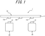
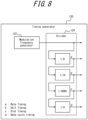
- FIG. 1 is a schematic diagram of a power wiring network apparatus 1 according to a first embodiment of the present disclosure.
- the power wiring network apparatus 1 includes a wiring member 10 and a plurality of circuit elements.
- the plurality of circuit elements include at least an energy harvesting element 20 and a load element 30, as illustrated in FIG. 1 . While details are provided below, each circuit element includes a second connector mechanically and electrically attachable to and detachable from any first connector along a plurality of first connectors 12a, 12b, 12c included in a wiring member 10 (for example, the energy harvesting element 20 includes a second connector 21, and the load element 30 includes a second connector 31).
- the plurality of circuit elements are electrically connected to each other in parallel via the wiring member 10.
- the shape of each component in the power wiring network apparatus 1 is prescribed for the sake of explanation, but the actual shapes of components are not limited to these shapes. This also applies to each of the drawings described below.
- the wiring member 10 is an elongated member overall that includes an elongated conductive portion 11 and three first connectors 12a, 12b, 12c.
- a power line capable of supplying power from the energy harvesting element 20 to the load element 30 is formed by the conductive portion 11 and the first connectors 12a, 12b, 12c.
- the power line can, for example, be a two-wire system.
- the wiring member 10 may include a covering that surrounds the conductive portion 11.
- Electric current can flow in the extending direction of the conductive portion 11 along the entire length thereof, for example.
- the conductive portion 11 includes an electrical conductor. Any electrical conductor may be included in the conductive portion 11. Examples include conductors made of a metal material such as copper, aluminum, gold, silver, nickel, and iron and conductors made of an alloy material including these metal materials.
- the conductive portion 11 may have sufficient flexibility to bend back at any point in the extending direction or may be rigid.
- the conductive portion 11 preferably has flexibility to provide the wiring member 10 with a variable shape and improve the degree of design freedom of the power wiring network apparatus 1 overall.
- the three first connectors 12a, 12b, 12c are each connected to the conductive portion 11. Accordingly, the three first connectors 12a, 12b, 12c are connected to each other in a conductive manner via the conductive portion 11, i.e. are electrically connected to each other. In the present embodiment, the three first connectors 12a, 12b, 12c are arranged at a distance from each other in the extending direction of the wiring member 10.
- FIG. 1 illustrates an example of the wiring member 10 including three first connectors 12a, 12b, 12c, but it suffices for the wiring member 10 to include a plurality of first connectors.
- the wiring member 10 may include two first connectors or may include four or more first connectors.
- the plurality of first connectors are conductively connected to each other.
- the plurality of first connectors may be arranged at a distance from each other along the extending direction of the wiring member 10.
- the plurality of first connectors may, for example, have the same shape.
- the three first connectors 12a, 12b, 12c are also referred to below as the first connector 12 when no distinction is made therebetween.
- the energy harvesting element 20 includes the second connector 21.
- the energy harvesting element 20 is capable of outputting, from the second connector 21, power generated by energy harvesting.
- FIG. 1 illustrates only one energy harvesting element 20, but the power wiring network apparatus 1 may include a plurality of energy harvesting elements 20. When a plurality of energy harvesting elements 20 are provided, the power generation capability of each energy harvesting element 20 may differ.
- the second connector 21 is mechanically and electrically attachable to and detachable from any of the first connectors 12 included in the wiring member 10.
- stating that two connectors are "mechanically and electrically attachable and detachable” refers to one of the connectors being attachable to the other connector and being detachable after attachment. In a state in which one connector is attached to the other connector, the two connectors are mechanically and electrically connected to each other. In a state in which one connector is detached from the other connector, the two connectors are mechanically and electrically disconnected from each other.
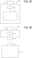
- FIGS. 2A and 2B are schematic views of configuration examples of the energy harvesting element 20 as a circuit element included in the power wiring network apparatus 1.
- FIG. 2A is a schematic view of an energy harvesting element 20a as a first configuration example of the energy harvesting element 20.
- FIG. 2B is a schematic view of an energy harvesting element 20b as a second configuration example of the energy harvesting element 20.
- the energy harvesting element 20a as the first configuration example of the energy harvesting element 20 includes an energy harvesting unit 22 and a reverse current prevention unit 23 in addition to the above-described second connector 21.
- the second connector 21 and the reverse current prevention unit 23 are electrically connected to each other via electrical wiring.
- the reverse current prevention unit 23 and the energy harvesting unit 22 are electrically connected to each other via electrical wiring.
- the electrical connection between the second connector 21 and the reverse current prevention unit 23 and the electrical connection between the reverse current prevention unit 23 and the energy harvesting unit 22 may be a direct connection, without the use of electrical wiring.
- the energy harvesting unit 22 is capable of generating power by energy harvesting. In other words, the energy harvesting unit 22 generates power in accordance with the external environment. Accordingly, the power generated by the energy harvesting unit 22 changes depending on the external environment.
- the energy harvesting unit 22 includes a solar cell, for example, that generates power using light energy such as sunlight or room light.
- the energy harvesting unit 22 may, for example, include a thermoelectric conversion element that generates power using thermal energy such as geothermal energy.
- the energy harvesting unit 22 outputs the generated power to the second connector 21 via the reverse current prevention unit 23.
- the energy harvesting unit 22 of the present embodiment includes a solar cell panel formed by a solar cell.
- the solar cell panel is a member including a solar cell that photoelectrically converts incident light such as sunlight, room light, or the like and outputs electric power.
- the types of solar cells included in the solar cell panel are roughly classified into inorganic solar cells in which an inorganic material is used and organic solar cells in which an organic material is used. Examples of inorganic solar cells include silicon (Si) solar cells in which silicon is used and compound solar cells in which a compound is used.
- organic solar cells include thin-film solar cells such as low-molecular weight vapor deposition-type solar cells in which an organic pigment is used, polymer coating-type solar cells in which a conductive polymer is used, and coating-conversion-type solar cells in which a conversion-type semiconductor is used; and dye-sensitized solar cells formed from titania, an organic dye, and an electrolyte.
- Solar cells included in a solar cell panel can also include organic/inorganic hybrid solar cells and solar cells in which a perovskite compound is used.
- the solar cell panel may be a thin panel. In this case, it is preferable to use a dye-sensitized solar cell, fabricated on a plastic film or the like, which is easy to form as a thin mold.
- the solar cell panel is not limited to one fabricated on a plastic film or the like; any mode is applicable as long as it is similarly thin.
- the thickness of the solar cell panel formed as a thin panel is preferably 10 ⁇ m or more to 3 mm or less, for example, from the perspective of manufacturing techniques.
- the reverse current prevention unit 23 prevents current from the second connector 21 from flowing into the energy harvesting unit 22.
- the reverse current prevention unit 23 can include a circuit element such as a diode. When a diode is used as the reverse current prevention unit 23, the diode is connected so that the anode is on the energy harvesting unit 22 side, and the cathode is on the second connector 21 side.
- the collector and the base terminals of a transistor may be connected and paired with the emitter for use as a diode in the reverse current prevention unit 23.
- the energy harvesting element 20b as the second configuration example of the energy harvesting element 20 includes the reverse current prevention unit 23 and a connector 24 for power generator connection, in addition to the above-described second connector 21.
- the energy harvesting element 20a includes the energy harvesting unit 22
- the energy harvesting element 20b differs by not including the energy harvesting unit 22.
- the reverse current prevention unit 23 included in the energy harvesting element 20b suppresses the flow of current from the second connector 21 into the connector 24 for power generator connection.
- the remaining configuration is similar to that of the above-described reverse current prevention unit 23 included in the energy harvesting element 20a.
- the connector 24 for power generator connection is a connector capable of mechanically and electrically connecting to an external energy harvesting unit 25.
- the connector 24 for power generator connection may be mechanically and electrically attachable to and detachable from the external energy harvesting unit 25.
- the connector 24 for power generator connection is not restricted, and a typical connector can be used.
- a connector conforming to a predetermined standard, such as a connector using a universal serial bus (USB) interface, can also be used.
- the external energy harvesting unit 25 has a similar configuration to that of the energy harvesting unit 22 included in the above-described energy harvesting element 20a.
- the connector 26 is a connector capable of mechanically and electrically connecting to the connector 24 for power generator connection. Like the connector 24 for power generator connection, the connector 26 is not restricted.
- the load element 30 includes the second connector 31.
- the load element 30 is capable of consuming power inputted from the second connector 31.
- the second connector 31 is mechanically and electrically attachable to and detachable from any of the first connectors 12 included in the wiring member 10.
- FIG. 1 illustrates only one load element 30, but the power wiring network apparatus 1 may include a plurality of load elements 30. When a plurality of load elements 30 is included, the power consumption of each load element 30 may differ.
- FIGS. 3A and 3B are schematic views of configuration examples of the load element 30 as a circuit element included in the power wiring network apparatus 1. Specifically, FIG. 3A is a schematic view of a load element 30a as a first configuration example of the load element 30. FIG. 3B is a schematic view of a load element 30b as a second configuration example of the load element 30.
- the load element 30a as the first configuration example of the load element 30 includes a load 32 and a voltage controller 33 in addition to the above-described second connector 31.
- the second connector 31 and the voltage controller 33 are electrically connected to each other via electrical wiring.
- the voltage controller 33 and the load 32 are electrically connected to each other via electrical wiring.
- the electrical connection between the second connector 31 and the voltage controller 33 and the electrical connection between the voltage controller 33 and the load 32 may be a direct connection, without the use of electrical wiring.
- the load 32 may be any load capable of consuming power.
- the load 32 may, for example, be an electronic device, such as a radio; an LED light; or the like.
- the power consumed by the load 32 may change depending on factors such as the drive state of the load 32.
- the voltage controller 33 controls the power inputted from the second connector 31 to be a predetermined voltage and outputs the result to the load 32.
- the voltage controller 33 steps down or steps up the power inputted from the second connector 31 to a predetermined voltage suitable for driving the load 32, such as the rated voltage of the load 32, and outputs the result to the load 32.
- the load element 30b as the second configuration example of the load element 30 includes the voltage controller 33 and a connector 34 for load connection in addition to the above-described second connector 31.
- the voltage controller 33 included in the load element 30b controls the power inputted from the second connector 31 to be a predetermined voltage and outputs the result to the connector 34 for load connection.
- the voltage controller 33 steps down or steps up the power inputted from the second connector 31 to a predetermined voltage such as the rated voltage according to the standards for the connector 34 for load connection and outputs the result to the connector 34 for load connection.
- the connector 34 for load connection is a connector capable of mechanically and electrically connecting to an external load 35.
- the connector 34 for load connection may be mechanically and electrically attachable to and detachable from the external load 35.
- the connector 34 for load connection is not restricted and may be a connector conforming to a predetermined standard, such as a connector using a USB interface.
- the external load 35 has a similar configuration to that of the load 32 included in the above-described load element 30a.
- the connector 36 is a connector capable of mechanically and electrically connecting to the connector 34 for load connection.
- the connector 36 is not restricted and may be a connector conforming to a predetermined standard, such as a connector using a USB interface. It suffices for the external load 35 to be capable of connecting, via the connector 36, to the connector 34 for load connection.
- the external load 35 may be a typical electronic device, such as a smartphone, a mobile phone, or a personal computer.
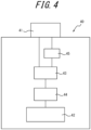
- the power wiring network apparatus 1 may further include a secondary battery element 40 as a circuit element.
- FIG. 4 is a schematic view of a configuration example of the secondary battery element 40 as a circuit element included in the power wiring network apparatus 1.
- the secondary battery element 40 includes a second connector 41.
- the second connector 41 is mechanically and electrically attachable to and detachable from any of the first connectors 12 included in the wiring member 10.
- the power wiring network apparatus 1 may include a plurality of secondary battery elements 40. When a plurality of secondary battery elements 40 is included, the input electric power during charging and the output electric power during power supply may differ between the secondary battery elements 40.
- the secondary battery element 40 includes a secondary battery 42, a switch 43, a voltage controller 44, and a reverse current prevention unit 45 in addition to the above-described second connector 41.
- the secondary battery 42 is capable of being charged and discharged.
- Examples of the secondary battery 42 include a lithium ion battery and a nickel-hydrogen battery.
- the switch 43 is capable of switching between a charging state of charging the secondary battery 42 with power inputted from the second connector 41 and a power supply state of outputting, from the second connector 41, power from the secondary battery 42.
- the switch 43 includes a switching element, for example, electrically connected between the second connector 41 and the secondary battery 42.
- the voltage controller 44 controls the power inputted from the second connector 41 to be a predetermined voltage and outputs the result to the secondary battery 42.
- the voltage controller 44 steps down or steps up the power inputted from the second connector 41 to a predetermined voltage suitable for charging the secondary battery 42, such as the rated voltage of the secondary battery 42, and outputs the result to the secondary battery 42.
- the voltage controller 44 also controls the power inputted from the secondary battery 42 to be a predetermined voltage and outputs the result to the second connector 41.
- the voltage controller 44 steps down or steps up the power inputted from the secondary battery 42 to a predetermined voltage suitable for another circuit element, such as a load element 30, and outputs the result to the second connector 41.
- the voltage controller 44 is connected between the switch 43 and the secondary battery 42 and is electrically connected to both.
- the reverse current prevention unit 45 suppresses current from the second connector 41 from flowing into the secondary battery 42.
- the reverse current prevention unit 45 can include a circuit element such as a diode.
- a diode is used as the reverse current prevention unit 45, the diode is connected so that the anode is on the secondary battery 42 side, and the cathode is on the second connector 41 side.
- the reverse current prevention unit 45 is positioned on the wiring so as to be conductive when the switch 43 is in the power supply state and not to be conductive when the switch is in the charging state.
- the power wiring network apparatus 1 includes a secondary battery element 40 in this way, power can be supplied to the load element 30 stably by switching between the charging state and the power supply state of the secondary battery element 40 depending on conditions.
- the secondary battery element 40 may be placed in the power supply state when power supply to the load element 30 is insufficient and be placed in the charging state when power supply to the load element 30 is sufficient.
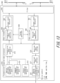
- FIG. 5 illustrates the configuration of a power wiring network apparatus 2 according to a second embodiment of the present disclosure.
- the power wiring network apparatus 2 includes two wiring members 10'.
- Each wiring member 10' further includes a third connector 13 and a fourth connector 14 in addition to the first connectors 12a, 12b, 12c.
- the third connector 13 is provided at one end of the wiring member 10' (the left end in FIG. 5 ).
- the fourth connector 14 is provided at the other end of the wiring member 10' (the right end in FIG. 5 ).
- the fourth connector 14 is mechanically and electrically attachable to and detachable from the third connector 13.
- all of the first connectors 12, the third connector 13, and the fourth connector 14 are electrically connected to each other by the conductive portion 11.
- a power line capable of supplying power from the energy harvesting element 20 to the load element 30 is formed by the conductive portion 11, the first connectors 12a, 12b, 12c, the third connector 13, and the fourth connector 14.
- the power line can, for example, be a two-wire system.
- One load element 30 is connected to the first connector 12a, one energy harvesting element 20 to the first connector 12b, and one secondary battery element 40 to the first connector 12c of one wiring member 10' (the left one in FIG. 5 ).
- One load element 30 is connected to the first connector 12a, one energy harvesting element 20 to the first connector 12b, and one load element 30 to the first connector 12c of the other wiring member 10' (the right one in FIG. 5 ).
- the use of two wiring members 10' can achieve a longer wiring member than a single wiring member 10' and enables an increase in the overall number of first connectors 12 to which circuit elements can be attached.
- the degree of freedom of arrangement can thereby be increased.
- the two wiring members 10' are configured to be connectable by a switching element 50.
- the switching element 50 includes a fifth connector 51, a sixth connector 52, and a switch 53.
- the fifth connector 51 is mechanically and electrically attachable to and detachable from the third connector 13 included in the wiring member 10'.
- the sixth connector 52 is mechanically and electrically attachable to and detachable from the fourth connector 14 included in the wiring member 10'.
- the fifth connector 51 and the sixth connector 52 in the present embodiment are provided at the left and right ends of the switching element 50 in FIG. 5 .
- the two wiring members 10' are basically arranged to be collinear by the third connector 13 of the wiring member 10' being connected to the fifth connector 51 and the fourth connector 14 of the wiring member 10' being connected to the sixth connector 52.
- the switch 53 can switch the fifth connector 51 and the sixth connector 52 between being electrically connected and disconnected.
- the switch 53 includes a switching element, for example, electrically connected between the fifth connector 51 and the sixth connector 52.
- the switch 53 may, for example, be configured so that between the fifth connector 51 and the sixth connector 52, an electrical connection for supplying DC power is switched between a connected and disconnected state, whereas an electrical connection for signal transmission by AC power (i.e. a C-connection or the like) is continuously maintained.
- the plurality of wiring members 10' can be switched between being electrically connected to and disconnected from each other by switching of the switch 53 in the switching element 50. Accordingly, when power is to be supplied preferentially to the load element 30 connected to the wiring member 10' on the right side of FIG. 5 , for example, the switch 53 can be disconnected when the power supply of the energy harvesting element 20 connected to the wiring member 10' on the right side is sufficient. Power is then supplied to the load element 30 from the energy harvesting element 20 connected to the wiring member 10' on the right side. When the power supply of the energy harvesting element 20 connected to the wiring member 10' on the right side is insufficient, the switch 53 can be connected.
- Power can then be supplied to the load element 30 connected to the wiring member 10' on the right side from the energy harvesting element 20 and the secondary battery element 40 connected to the wiring member 10' on the left side.
- power can thus be supplied on a priority basis to the load element 30 with a high priority for power supply.
- the switch 53 being disconnected, the energy harvesting element 20 and the load element 30 can be arranged for each wiring member 10'.
- a plurality of independent systems can be configured with any number of energy harvesting elements 20 and any number of load elements 30 combined in each system.
- the load element 30 connected to the first connector 12a of the wiring members 10' on the left and right is a circuit element for network management of the power wiring network apparatus 2.
- This circuit element includes a controller 101 configured by a central processing unit (CPU) or the like and functions as a network management device 100 configured as a load element 30 that receives power supplied from the power line.
- CPU central processing unit
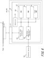
- FIG. 6 is a block diagram illustrating the configuration of the network management device 100 as a load element 30.
- the network management device 100 includes a controller 101 that controls the device overall, a logical data processor 103 that processes data transmitted and received to and from the power line, a wireless communication interface 105 for communicating with an external device 700 wirelessly, such as by Bluetooth or Wi-Fi ® (Wi-Fi is a registered trademark in Japan, other countries, or both), and a storage 106 that includes a read-only memory (ROM) 107, a random access memory (RAM) 108, and a rewritable flash ROM 109.
- the controller 101, the logical data processor 103, the wireless communication interface 105, and the storage 106 operate by receiving power supplied from the voltage controller 33 (see FIG. 3A ), not illustrated in FIG. 6 .
- the controller 101, the logical data processor 103, the wireless communication interface 105, and the storage 106 constitute the load 32 in FIG. 3A .
- the controller 101 controls the logical data processor 103, the wireless communication interface 105, the storage 106, and the like, as described below.
- the controller 101 can be configured by one or more CPUs, application specific integrated circuits (ASICs), digital signal processors (DSPs), programmable logic devices (PLDs), field programmable gate arrays (FPGAs), microcontrollers, or the like.
- ASICs application specific integrated circuits
- DSPs digital signal processors
- PLDs programmable logic devices
- FPGAs field programmable gate arrays
- microcontrollers or the like.
- the logical data processor 103 executes processing such as transmission and reception of data via the power line and generation of synchronization signals S1 to S4 for transmission and reception of data.
- the configuration of the logical data processor 103 is described in further detail below.
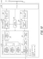
- FIG. 7 is a block diagram illustrating the configuration of the logical data processor 103.
- the logical data processor 103 includes a filter 170 for removing the DC component from electric power that includes a data signal supplied via the power line, a data receiver 140 for receiving and demodulating the data signal from which the DC component was removed to generate received data, a data transmitter 120 for modulating transmission data to generate a data signal to superimpose on the power line, a transmission/reception data processor 110 for performing signal processing on the received data and for generating transmission data, a timing generator 130 for generating a timing signal and the like for generation of the synchronization signals S1 to S4, and a synchronization signal generation unit 150 for generating the synchronization signals S1 to S4 that determine the transmission timing of transmission data and the like.
- the filter 170 has the function of removing the DC component from electric power that includes a data signal supplied via the power line.
- the filter 170 can, for example, be configured as a "C-connection" that connects the power line with the data receiver 140 and the data transmitter 190 using a capacitor.
- the filter 170 may be configured as a bandpass filter that only transmits signals in a particular band or be configured to include an active element such as an operational amplifier or a transistor.
- the data receiver 140 receives and demodulates the data signal from which the DC component was removed, thereby generating received data.
- the data receiver 140 includes a signal level adjuster 141 for adjusting the signal level and a received data demodulator 142 for demodulating the signal, after level adjustment, to generate the received data.
- the signal level adjuster 141 adjusts the signal amplitude so that the signal level of the data signal, from the power line, filtered by the filter 170 to include only the AC component falls within a predetermined range.
- the signal level adjuster 141 can be implemented by an automatic gain control circuit capable of adjusting the gain to be within a range suitable for the input signal level by feeding back the maximum signal level, for example.
- the received data demodulator 142 reads the level-adjusted data signal based on a timing signal from the timing generator 130 and demodulates the data signal that was modulated by another circuit element back to the original signal.
- the data signal may be demodulated by dedicated hardware or by software processing by the controller 101 or the like.
- the data transmitter 120 modulates the transmission data generated by the transmission/reception data processor 110 and superimposes the modulated transmission data on the power line via the filter 170.
- the data transmitter 120 includes a transmission data modulator 121 for modulating transmission data using a predetermined modulation method and a signal level adjuster 122 for adjusting the signal level.
- the transmission data modulator 121 digitally modulates the transmission data, generated by the transmission/reception data processor 110, using a predetermined modulation method.
- Orthogonal frequency division multiplexing (OFDM), spread spectrum (SS), or the like can be used as the modulation format, although these examples are not limiting.
- the transmission data modulator 121 outputs the modulated transmission data at an appropriate timing based on the timing signal from the timing generator 130 to input the modulated transmission data to the signal level adjuster 122.
- the signal level adjuster 122 adjusts the signal amplitude of the transmission data, modulated by the transmission data modulator 121, so that the signal level is suitable for superimposition on the power line.
- the transmission/reception data processor 110 processes the received data received by the data receiver 140 and generates the transmission data that serves as the basis for the data signal to be superimposed on the power line by the data transmitter 120.
- the transmission/reception data processor 110 includes a received data storage 116, a received data analyzer 117, and a device control information generation unit 118 as functional components for processing the received data.
- the transmission/reception data processor 110 includes a device attribute information generation unit 111, a command information generation unit 112, a status information generation unit 113, and a transmission data generation unit 115 as functional components for processing the transmission data.
- the received data demodulated by the data receiver 140 is stored in the received data storage 116 as necessary.
- the received data storage 116 may be configured as a dedicated storage for received data or as a partial area inside the RAM 108 of the storage 106, for example.
- the data stored in the received data storage 116 is analyzed by the received data analyzer 117.
- the received data is analyzed by determining whether the received data is attribute information, command information, or status information from another circuit element.
- attribute information the received data is analyzed by identifying the device that transmitted the attribute information, parameters of the attribute information, and the like.
- the received data is command information
- the received data is analyzed by identifying the device that transmitted the command information, the type of command ("command code" in Table 2), parameters, and the like.
- the received data is status information
- the received data is analyzed by identifying the device that transmitted the status information, the type of status ("status code" in Table 3), parameters, and the like.
- the received data may be analyzed by dedicated hardware or by software processing by the controller 101 or the like.
- the result of analysis of the received data by the received data analyzer 117 is processed by the device control information generation unit 118.
- the device control information generation unit 118 transmits the status information of the radio device 400 to the external device 700, such as a smartphone, via Bluetooth communication by the wireless communication interface 105. Consequently, by receiving the status information from the radio device 400, the user of the external device 700 can confirm whether operations by the user have been reflected in the state of the radio device 400.
- the transmission/reception data processor 110 includes the device attribute information generation unit 111, the command information generation unit 112, the status information generation unit 113, and the transmission data generation unit 115 as functional components for processing the transmission data.
- the below-described transmission data processing may be implemented by hardware or by software processing by the controller 101 or the like.
- the device attribute information generation unit 111 is a functional component for generating device attribute information in the format of the transmission data.
- the device attribute information is the device manufacturer, the device type, a device identifier, device characteristics, and the like.
- the device attribute information can, for example, be generated by reading related information from the ROM 107 and converting the related information to the format of the transmission data as necessary.
- the command information generation unit 112 is a functional component for generating command information in the format of the transmission data.
- the command information includes information with a recipient device number, a command code, a command parameter, and the like.
- the command information generation unit 112 receives a command issued in response to user operation on an application executed by the external device 700, such as a smartphone.
- the command information generation unit 112 receives the command by Bluetooth communication and generates a power line communication command corresponding to the received command.
- the command information generation unit 112 can generate a command to raise the volume of the radio for the radio device 400 (connected to the first connector 12c of the wiring member 10' at the right side in FIG. 5 ) corresponding to the command, received by Bluetooth communication, to raise the volume of the radio.
- the radio device 400 is one of the load elements 30 managed by the network management device 100.
- the status information generation unit 113 is a functional component for generating status information in the format of the transmission data.
- the status information includes information with a transmission device number, a status code, a status parameter, and the like.
- the status information generation unit 113 generates status information indicating that, for example, the network management device 100 has successfully received the attribute data of another circuit element (energy harvesting element 20, load element 30, or the like).
- the transmission data generation unit 115 Based on a timing signal from the timing generator 130, described below, the transmission data generation unit 115 outputs the transmission data, generated by each of the device attribute information generation unit 111, the command information generation unit 112, and the status information generation unit 113, in an appropriate order and at an appropriate timing to input the transmission data to the data transmitter 120.
- the synchronization signal generation unit 150 includes a synchronization signal generator 151 for generating the synchronization signals S1 to S4 based on the timing signal from the timing generator 130 and a signal level adjuster 152 for adjusting the signal amplitude so that the signal level of the synchronization signals S1 to S4 outputted from the synchronization signal generator 151 is suitable for superimposition on the power line.
- FIG. 8 is a block diagram illustrating the configuration of the timing generator 130.
- the timing generator 130 includes a modulation frequency generator 132 for generating a modulated wave modulated at a predetermined frequency and a frequency divider 134 for dividing the modulated wave from the modulation frequency generator 132 at a predetermined dividing ratio to obtain various timing signals.
- the cycle of the modulated wave outputted by the modulation frequency generator 132 corresponds to a period of one bit. Accordingly, one cycle of a timing signal a obtained by dividing the modulated wave from the modulation frequency generator 132 by eight corresponds to the period of one byte. One cycle of a timing signal b obtained by dividing the timing signal a by 10 corresponds to the period of one unit configured to have a length of 10 bytes, as described below. One cycle of a timing signal c obtained by further dividing the timing signal b by 4096 corresponds to the period of one slot configured to have a length of 4096 units, as described below.
- One cycle of a timing signal d obtained by further dividing the timing signal c by four corresponds to the period of one data cycle configured to have a length of four slots, as described below.
- the frequency of the modulated wave outputted by the modulation frequency generator 132 can, for example, be 100 kHz (the period of one bit thus becoming 0.01 msec), but this configuration is not limiting.
- the synchronization signal generator 151 illustrated in FIG. 7 generates pulses (synchronization signals S1 to S4), with a length of one unit, that rise synchronously with the slot timing signal (timing signal c) outputted by the timing generator 130.
- the modulated wave outputted by the modulation frequency generator 132 may be generated by dedicated hardware or be generated from a reference clock such as the CPU constituting the controller 101.
- the wireless communication interface 105 has the function of performing wireless communication conforming to a wireless communication standard such as Bluetooth or Wi-Fi.
- the wireless communication interface 105 communicates with the external device 700, such as a smartphone or tablet PC, and transmits a power line communication command, corresponding to a command received from the external device 700, to another device managed by the network management device 100.
- the wireless communication interface 105 can also transmit status information received from the other device to the external device 700.
- the storage 106 includes the ROM 107, the RAM 108, the rewritable, programmable flash ROM 109, and the like.
- the ROM 107 and the flash ROM 109 are both read-only memories, but the flash ROM 109 is writable and can store information such as programs to be executed by the CPU.
- the RAM 108 is a backup memory and is configured by dynamic random access memory (DRAM) or the like.
- the RAM 108 may include a volatile memory or non-volatile memory other than DRAM.
- the network management device 100 may be configured to include only a portion of the storage 106 illustrated in FIG. 6 or not to include the storage 106.
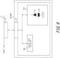
- FIG. 9 is a block diagram illustrating the configuration of an energy harvesting device 200 as the energy harvesting element 20.
- the energy harvesting device 200 includes a power generator 201, which includes the energy harvesting unit 22, and a logical data processor 203 that processes data transmitted to and received from the power line.
- the power generator 201 includes a solar cell as the energy harvesting unit 22 and a reverse current prevention unit 23 that suppresses current from the second connector 21 from flowing into the energy harvesting unit 22.
- the reverse current prevention unit 23 in the present embodiment is configured as a diode connected so that the cathode is on the second connector 21 side.
- the logical data processor 203 executes processing such as transmission and reception of data via the power line.
- FIG. 10 illustrates the configuration of the logical data processor 203.
- the logical data processor 203 has a configuration close to that of the logical data processor 103 illustrated in FIG. 7 , except that the configuration of a timing generator 230 differs, and the synchronization signal generation unit 150 is omitted.
- the logical data processor 203 includes the timing generator 230 that has a configuration partially differing from that of the timing generator 130 illustrated in FIG. 7 .
- the configuration of the timing generator 230 is illustrated in FIG. 11 .
- the timing generator 230 includes a signal level adjuster 231 for adjusting the signal level of the data signal, received from the power line via the filter 270, from which the DC component was removed, a synchronization signal detector 232 for detecting the synchronization signals S1 to S4 from the level-adjusted data signal, a voltage-controlled oscillator (VCO) 233, a divider 234, a phase comparator 235, and a low pass filter (LPF) 236.
- VCO voltage-controlled oscillator
- LPF low pass filter
- a phase comparison between the synchronization signals S1 to S4, on the data signal, that become input reference signals and the obtained timing signal makes it possible to obtain a timing signal synchronized with the synchronization signals S1 to S4 on the data signal and timing signals a' to d' yielded by dividing by a predetermined dividing ratio.
- one cycle of the timing signal a' obtained by division by eight corresponds to the period of one byte.
- One cycle of a timing signal b' obtained by dividing the timing signal a' by 10 corresponds to the period of one unit configured to have a length of 10 bytes, as described below.
- One cycle of a timing signal c' obtained by further dividing the timing signal b' by 4096 corresponds to the period of one slot configured to have a length of 4096 units, as described below.
- One cycle of a timing signal d' obtained by further dividing the timing signal c' by four corresponds to the period of one data cycle configured to have a length of four slots, as described below.
- a transmission/reception data processor 210 inside the logical data processor 203 may, for example, be configured to generate status information, in a status information generation unit 213, consisting of the generated power in the energy harvesting unit 22 and transmit the status information as transmission data to another device. In this way, another circuit element can effectively use the generated power from the energy harvesting element 20.
- a secondary battery device 300 as the secondary battery element 40 capable of supplying power to the load element 30, the power generator 201 in FIG. 9 is replaced by a battery unit 301 that includes the reverse current prevention unit 45, the switch 43, the voltage controller 44, and the secondary battery 42.
- a device control information generation unit 218 of the logical data processor 203 mounted in the secondary battery device 300 controls the switch 43 to switch the secondary battery 42 between a charging state and a discharging state.
- the device control information generation unit 218 may perform operations such as control of the voltage controller 44.
- the transmission/reception data processor 210 inside the logical data processor 203 may, for example, be configured to generate status information, in the status information generation unit 213, consisting of the stored electricity in the secondary battery 42 and transmit the status information as transmission data to another device. In this way, another circuit element can effectively use the electricity stored in the secondary battery 42.
- a radio device 400 as the load element 30, the power generator 201 in FIG. 9 is replaced by a radio 401.
- the device control information generation unit 218 of the logical data processor 203 mounted in the radio device 400 controls the radio 401 to change stations and adjust the volume.
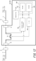
- FIG. 12 is a block diagram illustrating the configuration of the interrupting/conducting device 500 as the switching element 50.
- the interrupting/conducting device 500 includes a controller 501 for controlling the device overall, a logical data processor 503 for processing data transmitted to and received from the power line, a storage 506 including a ROM 507, a RAM 508, and the like, a switch 53 for switching the connection of two power lines that pass through the interrupting/conducting device 500, an I/O processor 505 for supplying a switching signal to the switch 53, and the fifth connector 51 and sixth connector 52 that connect to the wiring member 10' (power line).
- the fifth connector 51 and the sixth connector 52 are electrically connectable inside the switching element 50 (interrupting/conducting device 500) via the switch 53. Only one conductive portion of the two-wire conductive portion connecting the fifth connector 51 and the sixth connector 52 is illustrated in FIG. 12 .
- the controller 501, the logical data processor 503, and the storage 506 receive a supply of power from the power line to operate (the supply route from the power source is not illustrated).
- the interrupting/conducting device 500 may be configured to include only a portion of the storage 506 illustrated in FIG. 12 or not to include the storage 506.
- the controller 501 controls the logical data processor 503, the storage 506, the I/O processor 505, and the like, as described below.
- the controller 501 controls the switch 53 through control of the I/O processor 505, but the controller 501 may be configured to control the switch 53 directly.
- the controller 501 can be configured by one or more CPUs, application specific integrated circuits (ASICs), digital signal processors (DSPs), programmable logic devices (PLDs), field programmable gate arrays (FPGAs), microcontrollers, or the like.
- the logical data processor 503 executes processing such as transmission and reception of data via the power line. As illustrated in FIG. 13 , the logical data processor 503 has a configuration similar to that of the logical data processor 203 included in the energy harvesting device 200.
- the logical data processor 503 can exchange signal data with either or both of the wiring member 10' (power line) on the left side and the wiring member 10' (power line) on the right side of FIG. 5 . In other words, when the wiring members 10' on the left or right are disconnected by switching of the switch 53, the logical data processor 503 exchanges signal data with either the wiring member 10' (power line) on the left side or the wiring member 10' (power line) on the right side of FIG. 5 .
- a non-illustrated switching element controlled by the I/O processor 505 can be used to switch the logical data processor 503 between exchanging signal data with the wiring member 10' on the left and on the right.
- the selection of whether the logical data processor 503 exchanges signal data with the wiring member 10' on the left or the right may, for example, be made by the user with an application program on the external device 700, or the switching may occur at fixed intervals.
- a command is transmitted via the network management device 100 to the interrupting/conducting device 500.
- the wiring members 10' on the left and right are connected by switching of the switch 53, the same signal data is superimposed on the wiring members 10' on the left and right.
- the logical data processor 503 therefore exchanges signal data with the wiring members 10' on the left and right.
- DC power between the wiring members 10' on the left and right is interrupted by switching of the switch 53, an electrical connection for signal transmission by AC power may be maintained between the wiring members 10' on the left and right.
- the logical data processor 503 can exchange signal data with the wiring members 10' on the left and right.
- the same data signal is superimposed on the wiring members 10' on the left and right when the wiring members 10' on the left and right in FIG. 5 are connected by the switch 53, or when the wiring members 10' on the left and right are continually AC coupled.
- the network management device 100 connected to the wiring member 10' on the left side and the network management device 100 connected to the wiring member 10' on the right side in FIG. 5 are controlled so that only one functions as a network management device, whereas the other does not.
- the logical data processor 503 analyzes the received data from a data receiver 540 using a received data analyzer 517 and generates device control information in a device control information generation unit 518.
- the device control information is, for example, control information of the I/O processor 505, the ROM 507, the RAM 508, and the like.
- the device control information may be control information of the switching element for determining whether the logical data processor 503 exchanges signal data with the wiring member 10' on the left or the right.
- the I/O processor 505 controls switching elements in the switch 53 and the like by switching an output voltage between high and low and judges the state and the like of various devices based on an input voltage.
- the I/O processor 505 can be configured by an input/output port of a microcomputer as the controller 501, for example, or by dedicated hardware.
- FIG. 14 is a timing chart illustrating the modulated wave generated by the modulation frequency generator 132 and the various timing signals and synchronization signals S1 to S4 generated from the modulated wave.
- synchronization signals S1 to S4 are generated in the network management device 100, also referred to as "device 0", and the synchronization signals S1 to S4 are superimposed on DC power on the power line.
- each device transmits data, such as attribute data, a command code, or a status code, and receives data from other devices. Only the network management device 100 (device 0) transmits the synchronization signals S1 to S4 and the command code in the present embodiment.
- the network management device 100 (device 0) generates a modulated wave using the modulation frequency generator 132 in the timing generator 130 within the logical data processor 103.
- the modulated wave is a pulse signal having a cycle corresponding to a one bit period of the data signal, as illustrated by the uppermost portion of FIG. 14 .
- the timing generator 130 From this modulated wave, the timing generator 130 generates a byte timing signal corresponding to a period of one byte (timing signals a, a' in FIGS. 8 and 11 ), a unit timing signal corresponding to a period of one unit (timing signals b, b' in FIGS. 8 and 11 ), a slot timing signal corresponding to a period of one slot (timing signals c, c' in FIGS. 8 and 11 ), and a data cycle timing signal corresponding to a period of one data cycle (timing signals d, d' in FIGS. 8 and 11 ).
- One unit in the timing chart of FIG. 14 corresponds to a data length of 10 bytes. As indicated in the lowermost portion of FIG. 14 , data is transmitted and received in units of 10 bytes at a time during the power line communication of the present embodiment. One unit is formed by two bytes for space, two bytes for a header and a footer, and six bytes for data.
- FIG. 15 illustrates configuration examples of the header and the footer, but these examples are not limiting.
- One slot in the timing chart of FIG. 14 corresponds to a data length of 4096 units.
- the synchronization signals S1 to S4 are transmitted in this order from the network management device 100 (device 0) every slot, i.e. every 4096 units.
- each device can transmit 4095 units of a data signal after the synchronization signals S1 to S4 that have a length of one unit.
- the synchronization signals S1 to S4 and the header and footer in each unit can, for example, be defined as illustrated in the example of FIG. 15 .
- codes are allocated so that the first bit and the last bit become 1 in each signal. This enables the start position and end position of the code to be easily recognized from the data signal.
- the attribute data of each device is transmitted within the 4095 units following the synchronization signal S 1
- command data for each device is transmitted within the 4095 units following the synchronization signal S2
- status data from each device is transmitted within the 4095 units following the synchronization signal S3.
- each device upon detecting the synchronization signal corresponding to S 1 in FIG. 15 , each device can recognize that the attribute signal of each device is transmitted after S1.
- each device upon detecting the synchronization signal corresponding to S2 in FIG. 15 , each device can recognize that the command code for each device is transmitted after S2.
- each device can recognize that the status code for each device is transmitted after S3.
- FIG. 16 illustrates attribute data being transmitted and received for the case of at least three devices other than the network management device 100 (device 0) being connected to the wiring member 10.
- Devices 1, 2, 3, ... in FIG. 16 indicate the devices other than the network management device 100 (device 0).
- the attribute data transmitted by each device is allocated to a domain (i.e. slot 1) with a length of 4095 units after the synchronization signal S1 is outputted.
- the attribute data is transmitted from each device during this time domain.
- a length of one unit immediately after the synchronization signal S1 occurs is allocated to the network management device 100 (device 0). Only the network management device 100 (device 0) can transmit its own attribute data during the one unit immediately after the synchronization signal S1 occurs (in FIG. 16 , the network management device 100 (device 0) does not transmit its own attribute data).
- a length of one unit after the elapse of the unit allocated to the network management device 100 (device 0) is allocated to device 1 in the example of FIG. 16 .
- device 1 transmits its own attribute data by superimposing the attribute data on the power line as a data signal.
- the other devices receive the attribute data transmitted by device 1, recognize that device 1 is allocated as the device following device 0, and recognize the attributes of device 1. Accordingly, the attribute data from device 1 fulfills the role of a notification signal providing notification to other devices that device 1 is present.
- the network management device 100 (device 0) always receives the data signal during the 4095 units after the synchronization signal S1 and monitors all of the devices present within the network.
- the network management device 100 detects whether each device is present and detects the attribute data. Accordingly, the network management device 100 (device 0) can rapidly detect when a device is inserted or removed.
- Table 1 illustrates an example of attribute data of a device. [Table 1] Unit position Byte position Item Code Number of bytes 1 1 device manufacturer 10h 1 1 2 device type 40h 1 1 3 device identifier 11h 1 1 4-6 device characteristics 00 00 00h 3
- the item “device manufacturer” includes a code corresponding to the manufacturer of each device as the attribute data.
- the “device type” includes a code corresponding to the device type (for example, solar cell, secondary battery, passive load, active load, or the like) as attribute data.
- the “device identifier” includes a code corresponding to the device identifier (for example, speaker, radio, or the like) as attribute data.
- the item “device characteristics” includes a code corresponding to other characteristics of the device as the attribute data.
- the network management device 100 (device 0) is always used when the power wiring network apparatus 2 is used as a network system. When only the physical layer is used, however, the network management device 100 (device 0) need not be present.
- the network management device 100 is always allocated to device 0 (device number: 0) in the present embodiment.
- a length of one unit after the elapse of the unit for attribute data transmission allocated to device 1 is allocated to device 2 in the example of FIG. 16 .
- device 2 transmits its own attribute data by superimposing the attribute data on the power line as a data signal.
- the other devices can receive this attribute data transmitted from device 2.
- the network management device 100 (device 0) recognizes that device 2 is allocated as the device following device 1 and recognizes the attributes of device 2. Accordingly, the attribute data from device 2 fulfills the role of a notification signal providing notification to other devices that device 2 is present. The same holds for device 3.
- Each device continues to output attribute data at the timing allocated to the device until being disconnected from the wiring member 10'.
- the domain allocated for attribute data in slot 1 When the domain allocated for attribute data in slot 1 is insufficient, the domain may be expanded to other slots.
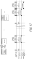
- FIG. 17 illustrates operations when device 2 is newly connected during a state in which only the network management device 100 (device 0) and device 1 are connected on the power line, as illustrated at the upper portion of FIG. 17 . Only the attribute data of device 1 is transmitted on the power line after output of the first synchronization signal S1 after device 2 is connected, as illustrated in FIG. 17 .
- the network management device 100 (device 0) only detects the attribute data of device 1 after output of the synchronization signal S1 and therefore recognizes that only device 1 is connected to the network.
- device 2 After the newly connected device 2 receives the first synchronization signal S1 after being connected, device 2 receives only the attribute data of device 1 and detects that the next unit after the attribute data of device 1 is a no-signal period. Device 2 receives the second synchronization signal S1, and during the no-signal period that is the next unit after receiving the attribute data of device 1, device 2 transmits its own attribute data.
- the network management device 100 (device 0) receives the attribute data of device 2 during the unit following the attribute data of device 1 and recognizes that device 2 is connected to the network in addition to device 1.
- the device newly connected to the network detects the no-signal period closest to the synchronization signal S1 after receiving S1 (excluding the period of one unit, immediately after the synchronization signal S 1, allocated to the network management device 100 (device 0)) and occupies the no-signal period as its own attribute data transmission period.
- the network management device 100 (device 0) recognizes the newly connected device (device 2 in the above example) by newly receiving the attribute data from newly connected device.
- the attribute data transmission period of the disconnected device becomes a no-signal period.
- a subsequently connected device detects this no-signal period and newly occupies the no-signal period as its own attribute data transmission period.
- the connector position where a device is inserted and the device number do not correspond.
- the device occupies the no-signal period closest to S1 as its own attribute data transmission period and acquires a device number corresponding to the time position of the no-signal period within slot 1.
- device 0 is always allocated to the network management device 100.
- the attribute data of each device is configured as fixed-length modulation data.
- This configuration as fixed-length modulation data enables each device to occupy a no-signal period of a fixed length, detected after receipt of the synchronization signal S1, as the device's own fixed-length attribute data transmission period. Since the attribute data is fixed length, the network management device 100 (device 0) can identify the device number of each set of attribute data from only the elapsed time after receipt of the synchronization signal S 1.
- FIG. 18 illustrates the state in which only device 1 is disconnected from the state illustrated in FIG. 17 .
- the network management device 100 (device 0) receives both the attribute data of device 1 and the attribute data of device 2 after transmitting the first synchronization signal S1 and recognizes that device 1 and device 2 are present on the network. After transmitting the second synchronization signal S1 in FIG. 18 , however, the network management device 100 (device 0) can only receive attribute data of device 2 and therefore recognizes that device 1 is not present on the network. The network management device 100 (device 0) recognizes that device 2 is present on the network and continues to exchange data with device 2.
- FIG. 19 illustrates a state in which the network management device 100 (device 0) and devices 1 to 3 are connected on the power line.
- FIG. 19 illustrates how, in this state, a command code is transmitted and received after receipt of the synchronization signal S2, and a status code is transmitted and received after receipt of the synchronization signal S3.
- Devices 1 to 3 are devices other than the network management device 100.
- Device 3 is assumed to be the radio device 400 as a load element 30.
- the timing chart of devices 1, 2 in FIG. 19 is omitted.
- the network management device 100 (device 0) and devices 1 to 3 are connected to the network illustrated in the upper portion of FIG. 19 . Therefore, attribute data from devices 1 to 3 is superimposed on the power line after transmission of the synchronization signal S1 (slot 1).
- the synchronization signal S2 from the network management device 100 (device 0) is transmitted and superimposed on the power line.
- the command code transmitted by each device is allocated to a domain (i.e. slot 2) with a length of 4095 units after the synchronization signal S2 is outputted.
- the command code is transmitted from the network management device 100 (device 0) during this time domain.
- a command with a length of two units is transmitted from the network management device 100 (device 0) at the time position of the third unit after the synchronization signal S2 is transmitted.
- Table 2 illustrates an example of command information.
- the item "command recipient” designates the recipient of the command by device number.
- the item “command allocation unit number” designates the unit in slot 2 in which the command is to be transmitted.
- the “command length” designates the length of the command as a number of units.
- the "command code” is a code corresponding to an instruction (control information) for each device and is variable length data.
- the "command parameter” is a parameter appended to the command and is transmitted simultaneously with the command. In the example in Table 2, the command is transmitted to device 3, the command is transmitted in the third unit of slot 2, the command length is two units, and the command code is "0800h".
- the commands transmittable to the radio device 400 include “power on”, “power off”, “change AM station”, “change FM station”, and “adjust volume”, for example.
- the station frequency can be increased or decreased by a command parameter being transmitted together with the command.
- the volume can be raised or lowered by a command parameter being transmitted together with the command.
- the command length can be changed in the present embodiment.
- a command code containing control information of a device can be transmitted as variable length data. This enables flexible support for devices in accordance with the type of command (control information) or the like and also enables a plurality of circuit elements to share a power line communication environment efficiently.
- the synchronization signal S3 from the network management device 100 (device 0) is transmitted and superimposed on the power line.
- the status code transmitted by each device is allocated to a domain (i.e. slot 3) with a length of 4095 units after the synchronization signal S3 is outputted.
- the status code is transmitted from each device (device 0 to device 3 in the example of FIG. 19 ) during this time domain.
- a status code with a length of two units is transmitted from device 3 at the time position of the third unit after the synchronization signal S3 is transmitted.
- Table 3 illustrates an example of status information.
- the item “status sender” designates the sender of the status information by device number.
- the item “status allocation unit number” designates the unit in slot 3 in which the status information is to be transmitted.
- the “status length” designates the length of the status as a number of units.
- the “status code” is a code corresponding to the status information from each device and is variable length data.
- the “status parameter” is a parameter appended to the status and is transmitted simultaneously with the status. In the example of Table 3, the status is transmitted from device 3, the status is transmitted in the third unit of slot 3, the status length is two units, and the status code is "0800h”.
- the status transmittable from each device is "normal execution” or "execution error", for example.
- an error code may be transmitted as a status parameter simultaneously with the status code.
- the status length can be changed in the present embodiment.
- a status code containing status information of a device can be transmitted as variable length data. This enables flexible support for devices in accordance with the type of status or the like and also enables a plurality of circuit elements to share a power line communication environment efficiently.
- FIGS. 20A and 20B are flowcharts illustrating the flow of transmission and reception of commands and status between the network management device 100 (device 0) and the radio device 400 (device 3).
- the network management device 100 (device 0) performs initial settings such as initialization of the controller 101 (step S101) and then transmits the synchronization signal S1 (step S103). After transmitting the synchronization signal S1, the network management device 100 (device 0) judges whether attribute data of another device is present in slot 1 (step S105) and receives all of the attribute data in slot 1 when judging that attribute data is present (step S107). Attribute data is not received when it is judged that attribute data is not present in step S105.
- the network management device 100 (device 0) transmits the synchronization signal S2 after a length of 4095 units elapses after transmission of the synchronization signal S 1 (step S 109). Transmission of the synchronization signal S2 marks the transition from slot 1 to slot 2, and commands can be transmitted and received.
- the network management device 100 (device 0) confirms whether a user command from the external device 700 is present via the wireless communication interface 105 (step S111) and transmits a power line communication command, corresponding to the user command, for device 3 in slot 2 when the user command is confirmed as being present (step S113).
- the network management device 100 (device 0) transmits the synchronization signal S3 after a length of 4095 units elapses after transmission of the synchronization signal S2 (step S115). Transmission of the synchronization signal S3 marks the transition from slot 2 to slot 3, and the status can be transmitted and received.
- the network management device 100 (device 0) monitors the status during slot 3, i.e. until a length of 4095 units elapses after transmission of the synchronization signal S3. Upon detecting the status (step S117), the network management device 100 (device 0) receives the status and transmits the status information via the wireless communication interface 105 to the external device 700 (step S119).
- the radio device 400 (device 3) When the radio device 400 (device 3) is connected to the power line by insertion of the second connector 31 into the first connector 12 (step S201), the radio device 400 (device 3) searches for a no-signal period in slot 1 (step S203). Upon detecting a no-signal period, the radio device 400 (device 3) occupies the no-signal period closest to the synchronization signal S1 after reception of S1 as its own attribute data transmission period and acquires a device number, corresponding to the time position of the no-signal period, as the device number of the radio device 400 (device 3) (step S205).
- the radio device 400 (device 3) When the radio device 400 (device 3) receives the synchronization signal S1 the next time, the radio device 400 (device 3) transmits its own attribute data at the time position it occupies as its own attribute data transmission period after the synchronization signal S1 (step S207). Subsequently as well, the radio device 400 (device 3) searches for the third unit position that it occupies as its own attribute data transmission period in slot 1 (step S209) and transmits its own attribute data (step S211).
- the radio device 400 (device 3) monitors for a command for itself in slot 2 after transmitting its own attribute data (step S213).
- the radio device 400 (device 3) confirms whether a command is for the radio device 400 (device 3) by whether its own device number is designated in the item "command recipient" of Table 2.
- the radio device 400 (device 3) receives the command and transmits a command execution result as a status in slot 3 (step S215).
- the present embodiment includes a wiring member 10', including a plurality of first connectors 12 and a conductive portion 11 electrically connecting the plurality of first connectors 12 in a manner capable of supplying power, and a plurality of circuit elements each including a second connector 21, 31, 41 mechanically and electrically attachable to and detachable from any first connector 12 among the plurality of first connectors 12.
- the plurality of circuit elements includes an energy harvesting element 20 as a circuit element capable of outputting, from the second connector 21, power generated by energy harvesting and a load element 30 as a circuit element capable of consuming power inputted from the second connector 31. At least some of the energy harvesting elements 20 and the load elements 30 are capable of power line data communication via a power line including the first connectors 12 and the conductive portion 11. This configuration enables the construction of a power wiring network with excellent portability, without the need to maintain infrastructure.
- the energy harvesting element 20 (energy harvesting device 200) includes a data transmitter 220 configured to transmit data via the second connector 21. This configuration enables another circuit element to be notified, via the data transmitter 220, that the energy harvesting element 20 is connected to the network. Furthermore, the state of the energy harvesting element 20 can be transmitted to another circuit element, enabling efficient use of the power generated by the energy harvesting element 20.
- At least one load element 30 (network management device 100) includes the data transmitter 120 configured to transmit data via the second connector 31 and includes the data receiver 140 configured to receive data.
- This configuration enables another circuit element to be notified, via the data transmitter 120, that the load element 30 is connected to the network.
- the load element 30 can receive a command via the data receiver 140, enabling the user to operate the load element 30 by power line communication.
- the data transmitters 120, 220 are capable of transmitting a signal yielded by digital modulation of transmission data to another circuit element by superimposing the signal on the power line via the second connector 21, 31. This configuration enables high-speed communication using a power wiring network.
- the data receiver 140 is configured to receive, via the second connector 31, a signal yielded by digital modulation and superimposed on the power line and is configured to demodulate the signal and generate received data. This configuration enables high-speed communication using a power wiring network.
- At least one load element 30 (network management device 100) is capable of generating the synchronization signal S1 and of transmitting the synchronization signal S1 to another circuit element, the synchronization signal S1 being for determining the timing of generation of a notification signal for the energy harvesting element 20 or the load element 30 to notify another circuit element that the energy harvesting element 20 or the load element 30 is present.
- This configuration enables the network management device 100 to easily detect a circuit element in the network.
- the energy harvesting element 20 or the load element 30 is configured to receive the synchronization signal S1 and to transmit the notification signal of the energy harvesting element 20 or the load element 30 to another circuit element during a predetermined period based on the synchronization signal when the energy harvesting element 20 or the load element 30 detects no signal during the predetermined period.
- This configuration enables stable communication in accordance with current conditions when a circuit element is added during operation of the network. Furthermore, when a circuit element is removed during operation of the network, the network management device 100 can easily detect the removal of the circuit element.
- the notification signal includes attribute data of the energy harvesting element 20 or the load element 30, and the attribute data is fixed length modulation data.
- the attribute data is fixed length modulation data.
- At least one load element 30 (network management device 100) is configured to transmit variable length data including control information of the energy harvesting element 20 or the load element 30. This configuration enables efficient sharing of the power line communication environment among a plurality of circuit elements.
- At least one energy harvesting element 20 or load element 30 is configured to transmit variable length data including status information of the at least one energy harvesting element 20 or load element 30. This configuration enables efficient sharing of the power line communication environment among a plurality of circuit elements.
- the circuit elements include the switching element 50 capable of switching a plurality of the power lines between being electrically connected to and disconnected from each other.
- This configuration enables power lines to be separated into a plurality of local networks or integrated into one network. Accordingly, an entire local network can be added to another network.
- a plurality of local networks can be continually AC coupled, thereby enabling DC power to be cut off between the local networks by the switching element 50 while network communication is enabled between the local networks.
- the switching element 50 includes the data transmitter 520 configured to transmit data and the data receiver 540 configured to receive data. This configuration enables another circuit element to be notified, via the data transmitter 520, that the switching element 50 is connected to the network. Furthermore, the switching element 50 can receive a command via the data receiver 540, enabling the user to operate the switching element 50 by power line communication.
- the load element 30 capable of generating the synchronization signal S1 is further capable of wireless communication by Bluetooth. This configuration enables a user to use circuit elements, which are connected to the power wiring network, by communicating wirelessly with the network management device 100 from the external device 700 such as a smartphone.
- FIGS. 21A and 21B are schematic diagrams (a rear view and a plan view) of a power wiring network apparatus 61 according to a third embodiment of the present disclosure.
- the present embodiment illustrates a different embodiment for the physical layer of the power wiring network apparatus than in the first and second embodiments.
- the power wiring network apparatus 61 includes a wiring member 70 and circuit elements 80.
- the wiring member 70 is formed to have a plate-like planar shape, as illustrated in FIGS. 21A and 21B , and includes a plurality of seventh connectors 72.
- the power wiring network apparatus 61 includes at least one energy harvesting element inside at least any one of the circuit elements 80.
- the circuit element 80 is formed to be plate-like and includes an eighth connector 81 mechanically and electrically attachable to and detachable from any seventh connector 72 among the plurality of seventh connectors 72 provided in the wiring member 70.
- the plurality of seventh connectors 72 are connected to each other electrically by a conductive portion 71B, and the circuit elements 80 attached to the plurality of seventh connectors 72 are connected to each other electrically by the conductive portion 71B.
- FIGS. 21A and 21B the shape of each component in the power wiring network apparatus 61 is prescribed for the sake of explanation, but the actual shapes of components are not limited to these shapes. This also applies to each of the drawings described below.
- the surface direction of the wiring member 70 and the circuit element 80 refers to the direction parallel to the paper in FIG. 21B
- the thickness direction of the wiring member 70 and the circuit element 80 refers to the direction perpendicular to the paper in FIG. 21B
- the upper surface of the wiring member 70 and the circuit element 80 indicates the surface visible in the plan view of FIG. 21B .
- the seventh connector 72 and an edge holding member 74A are provided on the upper surface of the wiring member 70.
- the left-right direction of the wiring member 70 and the circuit element 80 is the left-right direction in FIG. 21B .
- the wiring member 70 is provided with a board body 71A made of an insulating material, two seventh connectors 72, a conductive portion 71B electrically connecting the seventh connectors 72, an edge holding member 74A holding the edges of the circuit element 80, and a ninth connector 73.
- the wiring member 70 according to the present embodiment is a planar member that has a rectangular shape in plan view.
- the wiring member 70 may include a covering, formed by an insulating material, that surrounds the conductive portion 71B.
- the wiring member 70 can be configured by a board that includes wiring as the conductive portion 71B.
- the board may be a rigid board, such as a glass epoxy board or paper phenol board, or a flexible printed circuit board made of polyimide film or the like.
- a reinforcing plate is preferably provided in the area where electronic components and members such as the edge holding member 74A, described below, are mounted. The reinforcing plate ensures the rigidity of the board body 71A.
- the surface is preferably covered with a covering material, such as cloth or resin, from the perspective of design and resistance to the environment.
- the conductive portion 71B includes an electrical conductor. Any electrical conductor may be included in the conductive portion 71B. Examples include conductors made of a metal material such as copper, aluminum, gold, silver, nickel, and iron and conductors made of an alloy material including these metal materials.
- the conductive portion 71B may have sufficient flexibility to bend back at any point in the extending direction or may be rigid.
- the conductive portion 71B preferably has flexibility to provide the wiring member 70 with a variable shape and improve the degree of design freedom of the power wiring network apparatus 61 overall.
- the two seventh connectors 72 are each connected to the conductive portion 71B. Accordingly, the two seventh connectors 72 are electrically connected to each other in a conductive manner via the conductive portion 71B. In the present embodiment, the two seventh connectors 72 are arranged at a distance from each other along the longitudinal direction (the left-right direction in FIG. 21B ) of the wiring member 70.
- the ninth connector 73 may be provided at the edge of the wiring member 70 as illustrated in FIG. 21B . When the ninth connector 73 is provided on the wiring member 70, the two seventh connectors 72 along with the ninth connector 73 are electrically connected via the conductive portion 71B.
- FIGS. 21A and 21B illustrate an example of the wiring member 70 including two seventh connectors 72, but it suffices for the wiring member 70 to include a plurality of seventh connectors 72.
- the wiring member 70 may include three or more seventh connectors 72.
- the plurality of seventh connectors 72 are conductively connected to each other.
- the plurality of seventh connectors 72 may be arranged at a distance from each other along the longitudinal direction of the wiring member 70 but are not limited to this configuration.
- the plurality of seventh connectors 72 may, for example, have the same shape.
- the edge holding member 74A is provided in the area surrounding the circuit element 80 in plan view of the wiring member 70, as illustrated in FIG. 21B .
- the edge holding member 74A includes a housing 75A that houses the edges of the circuit element 80 along the insertion and removal direction of the eighth connector 81 (indicated by the arrow in FIG. 21B ).
- the housing 75A is configured to cover the upper surface and side surfaces of the edges in the left-right direction of the circuit element 80, as illustrated in FIG. 21A .
- the eighth connector 81 is thus positioned to be attachable to the seventh connector 72.
- the edge of the circuit element 80 is depicted as having been housed in the housing 75A of the edge holding member 74A at the left side of FIG. 21B , and the eighth connector 81 is depicted as having been attached to the seventh connector 72.
- the housing 75A extends not only over the area at the left and right edges of the circuit element 80, but also over the area of the edges adjacent to the left and right of the seventh connector 72 and the area of the edge of the circuit element 80 opposite the seventh connector 72. Accordingly, all four edges of the rectangular circuit element 80 are housable in the housing 75A.
- the housing 75A at the insertion side when the circuit element 80 is inserted in the edge holding member 74A (the upper side in FIG. 21B , i.e. the housing 75A at the side opposite the seventh connector 72), however, does not restrict the circuit element 80 in the surface direction.
- the circuit element 80 is insertable in the edge holding member 74A from the side opposite the seventh connector 72 in FIG.
- a rectangular opening 74A1 is formed at the central position of the edge holding member 74A in the surface direction, as illustrated in FIG. 21B .
- sunlight can strike the solar cell through the opening 74A1 for power to be generated.
- Displacement of the circuit element 80 in the thickness direction is reliably restricted by the housing 75A thus housing all four edges of the circuit element 80, which is rectangular in plan view. Accordingly, even when the power wiring network apparatus 61 is carried with the circuit element 80 attached to the wiring member 70, the circuit element 80 and the wiring member 70 can be stably held in a parallel state so that the circuit element 80 does not separate from the upper surface of the wiring member 70. Furthermore, the circuit element 80 is positioned in the left-right direction relative to the edge holding member 74A by the left and right sides of the circuit element 80 abutting against the edge holding member 74A. The eighth connector 81 can therefore be positioned to be attachable to the seventh connector 72.
- the circuit element 80 When the edges of the circuit element 80 are housed in the housing 75A of the edge holding member 74A in this way, the circuit element 80 can be moved in parallel with the wiring member 70 for easy attachment of the eighth connector 81 to the seventh connector 72. Furthermore, the stress on each member when the eighth connector 81 is attached to the seventh connector 72 can be reduced.
- the circuit element 80 has a rectangular shape in plan view, but this example is not limiting. It suffices for at least a portion of the left and right edges of the circuit element 80 to be linear. The reason is that housing this linear portion in the edge holding member 74A enables the eighth connector 81 to be positioned relative to the seventh connector 72 and mounted while the circuit element 80 is maintained parallel to the wiring member 70.
- the shape of the circuit element 80 need not have a linear portion on the edges and may instead have a shape formed only by curves, such as a circle.
- the shape of the housing 75A of the edge holding member 74A may also be curved as appropriate in correspondence with the shape of the edges of the circuit element 80.
- the wiring member 70 (board body 71A) need not be disposed over the entire area where the circuit element 80 is mounted on the wiring member 70. To reduce weight, the wiring member 70 (board body 71A) may be disposed only in the portion for supporting the circuit element 80, such as the portion in contact with the perimeter of the circuit element 80.
- the circuit element 80 includes the eighth connector 81.
- the eight connector 81 of a circuit element 80 has been attached to the seventh connector 72 on the left, and the eighth connector 81 of a circuit element 80 is about to be attached to the seventh connector 72 on the right.
- the eighth connector 81 in the example illustrated in FIG. 21B is provided on an edge of the circuit element 80.
- the insertion and removal direction of the eighth connector 81 relative to the seventh connector 72 is the up-down direction in FIG. 21B and is parallel to the surface direction of the circuit element 80. Consequently, the circuit element 80 does not project in the thickness direction when attached or detached, enabling a reduction in the thickness of the power wiring network apparatus 61 that takes into account attachment and detachment of the circuit element 80. Furthermore, when the circuit element 80 is attached or detached, it suffices to exert a force in the surface direction of the circuit element 80. This configuration can suppress an excessive stress, such as bending stress, on each member. In the example in FIG. 21B , the insertion and removal direction of the eighth connector 81 relative to the seventh connector 72 is also parallel to the surface direction of the wiring member 70.
- the circuit element 80 can, for example, include an energy harvesting element.
- the energy harvesting element is capable of outputting, from the eighth connector 81, power generated by energy harvesting.
- the power generation capability of the energy harvesting elements may differ.
- At least one circuit element 80 between the two circuit elements 80 connected to the two seventh connectors 72 of FIG. 21B includes an energy harvesting element. Consequently, power generated by energy harvesting can be outputted from the eighth connector 81, and power can be supplied to a load element connected to the wiring member 70.
- the eighth connector 81 is mechanically and electrically attachable to and detachable from any of the seventh connectors 72 included in the wiring member 70.
- stating that two connectors are "mechanically and electrically attachable and detachable" refers to one of the connectors being attachable to the other connector and being detachable after attachment. In a state in which one connector is attached to the other connector, the two connectors are mechanically and electrically connected to each other. In a state in which one connector is detached from the other connector, the two connectors are mechanically and electrically disconnected from each other.
- the energy harvesting element mounted in the circuit element 80 can, for example, be configured to include an energy harvesting unit (not illustrated), capable of generating power by energy harvesting, and a reverse current prevention unit (not illustrated).
- the energy harvesting unit generates power in accordance with the external environment and includes a solar cell, for example, that generates power using light energy such as sunlight or room light.
- the energy harvesting unit may include a thermoelectric conversion element that generates power using thermal energy such as geothermal energy.
- the energy harvesting unit outputs the generated power to the eighth connector 81 via the reverse current prevention unit.
- the reverse current prevention unit prevents current from the eighth connector 81 from flowing into the energy harvesting unit.
- the reverse current prevention unit can include a circuit element such as a diode. When a diode is used as the reverse current prevention unit, the diode is connected so that the anode is on the energy harvesting unit side, and the cathode is on the eighth connector 81 side.
- the collector and the base terminals of a transistor may be connected and paired with the emitter for use as a diode in the reverse current prevention unit.
- the energy harvesting unit may be an energy harvesting unit included in another circuit element connected via the circuit element 80.
- the circuit element 80 can include a load element.
- the load element is capable of consuming power inputted from the eighth connector 81.
- one circuit element 80 of the two circuit elements 80 attached via the two seventh connectors 72 may include an energy harvesting element, whereas the other circuit element 80 may include a load element.
- At least one of the circuit elements 80 may include a load element together with an energy harvesting element.
- the circuit element 80 may include a charged secondary battery element, described below, or may be configured to supply auxiliary power to the load element from another apparatus via the ninth connector 73.
- the power consumption of each load element may differ.
- the circuit element 80 can include a load and a voltage controller in addition to the eighth connector 81.
- the eighth connector 81 and the voltage controller are electrically connected to each other directly or via electrical wiring.
- the voltage controller and the load are electrically connected to each other directly or via electrical wiring.
- the voltage controller controls the power inputted from the eighth connector 81 to be a predetermined voltage and outputs the result to the load.
- the voltage controller steps down or steps up the power inputted from the eighth connector 81 to a predetermined voltage suitable for driving the load, such as the rated voltage of the load, and outputs the result to the load.
- the power wiring network apparatus 61 may further include a secondary battery element as a circuit element.
- the circuit element 80 can include a secondary battery, a switch, a voltage controller, and a reverse current prevention unit, for example, in addition to the above-described eight connector 81.
- the switch is capable of switching between a charging state of charging the secondary battery with power inputted from the eighth connector 81 and a power supply state of outputting, from the eighth connector 81, power from the secondary battery.
- the switch includes a switching element, for example, electrically connected between the eighth connector 81 and the secondary battery.
- the voltage controller controls the power inputted from the eighth connector 81 to be a predetermined voltage and outputs the result to the secondary battery.
- the voltage controller steps down or steps up the power inputted from the eighth connector 81 to a predetermined voltage suitable for charging the secondary battery, such as the rated voltage of the secondary battery, and outputs the result to the secondary battery.
- the voltage controller also controls the power inputted from the secondary battery to be a predetermined voltage and outputs the result to the eighth connector 81.
- the voltage controller steps down or steps up the power inputted from the secondary battery to a predetermined voltage suitable for another circuit element, such as a load element, and outputs the result to the eighth connector 81.
- the reverse current prevention unit suppresses current from the eighth connector 81 from flowing into the secondary battery.
- the reverse current prevention unit can include a circuit element such as a diode. When a diode is used as the reverse current prevention unit, the diode is connected so that the anode is on the secondary battery side, and the cathode is on the eighth connector 81 side.
- the circuit element 80 includes a secondary battery element in this way, power can be supplied to the load element stably by switching between the charging state and the power supply state of the secondary battery element depending on conditions.
- the secondary battery element may be placed in the power supply state when power supply to the load element is insufficient and be placed in the charging state when power supply to the load element is sufficient.
- FIG. 22 is a schematic diagram (perspective view) of a power wiring network apparatus 90 according to a fourth embodiment of the present disclosure.
- the power wiring network apparatus 90 is a modification to the power wiring network apparatus 61 illustrated in FIGS. 21A and 21B .
- Four seventh connectors 72 in the left-right direction and three in the up-down direction of FIG. 22 are arranged in a matrix on the upper surface of a wiring member 70C, for a total of 12 seventh connectors 72.
- a bending position 70b2 extending in the up-down direction of FIG. 22 is defined at an in-plane position, between two seventh connectors 72 adjacent in the left-right direction, where no external circuit element 80 is disposed.
- seventh connectors 72 opposite each other do not completely overlap but rather are separated in the up-down direction of FIG. 22 substantially by the vertical length of the circuit element 80.
- two seventh connectors 72 adjacent to a bending position 70b2 are disposed at in-plane positions that do not overlap in the surface direction when the wiring member 70C is bent at the bending position 70b2. Accordingly, the thickness in the direction of overlap when the power wiring network apparatus 90 is bent can be reduced, thereby increasing the portability of the power wiring network apparatus 90.
- the configuration of the power wiring network apparatus 90 can be achieved by, for example, forming the wiring member 70C as a flexible printed circuit board, providing a reinforcing plate in the area where the circuit element 80 is disposed to ensure rigidity of the wiring member 70C, and not providing a reinforcing plate at the bending position 70b2.
- the configuration of the power wiring network apparatus 90 may also be achieved by using a circuit board in which a rigid board and a flexible printed circuit board are integrated and arranging the flexible printed circuit board at the bending position 70b2.
- Any of the energy harvesting elements included among the circuit elements of the first, third, and fourth embodiments described above can operate as the energy harvesting device 200 of the second embodiment.
- Any of the load elements included among the circuit elements of the first, third, and fourth embodiments described above can operate as the network management device 100, the radio device 400, or the like of the second embodiment.
- Any of the secondary battery elements included among the circuit elements of the first, third, and fourth embodiments described above can operate as the secondary battery device 300 of the second embodiment.
- One connector may be male and the other female, for example.
- the second connector (for example, the second connector 21, 31, and 41) that is attachable to and detachable from the first connector 12 is a female connector.
- the first connector 12 is a male connector
- the second connector that is attachable to and detachable from the first connector 12 is a male connector.
- the fourth connector 14 and fifth connector 51 that are attachable to and detachable from the third connector 13 are female connectors
- the sixth connector 52 that is attachable to and detachable from the fourth connector 14 is a male connector
- the third connector 13 is a female connector
- the fourth connector 14 and fifth connector 51 that are attachable to and detachable from the third connector 13 are male connectors
- the sixth connector 52 that is attachable to and detachable from the fourth connector 14 is a female connector.
- a configuration such that the third connector 13 and the first connector 12 are the same and the fourth connector 14 and the second connector are the same may be adopted.
- a configuration such that the third connector 13 and the second connector are the same and the fourth connector 14 and the first connector 12 are the same may be adopted.
- Both the third connector 13 and the fourth connector 14 may be the same as the first connector 12.
- the fifth connector 51 and the sixth connector 52 may be the same as the second connector.
- Both the third connector 13 and the fourth connector 14 may be the same as the second connector.
- the fifth connector 51 and the sixth connector 52 may be the same as the first connector 12.
- the energy harvesting element 20 need not include the reverse current prevention unit 23.
- the energy harvesting element 20 preferably includes the reverse current prevention unit 23, however, to help prevent current from circuit elements such as other energy harvesting elements 20 from flowing into the energy harvesting unit 22 or into an external energy harvesting unit 25.
- the energy harvesting element 20 may include a voltage controller to control the output voltage to be constant.
- the load element 30 need not include the voltage controller 33.
- the load element 30 preferably includes the voltage controller 33, however, to help prevent power from circuit elements such as the energy harvesting element 20 from being inputted to the load 32 or the external load 35 at higher than rated voltage, for example.
- the secondary battery element 40 need not include the voltage controller 44.
- the secondary battery element 40 preferably includes the voltage controller 44, however, so as to control the voltage of power inputted to and outputted from the secondary battery 42.
- the secondary battery element 40 need not include the reverse current prevention unit 45.
- the secondary battery element 40 preferably includes the reverse current prevention unit 45, however, to help prevent current from circuit elements such as other energy harvesting elements 20 from flowing into the secondary battery 42 when the switch 43 is in the power supply state.
- the load element 30, the energy harvesting element 20, the secondary battery element 40, and the switching element 50 can be freely combined.
- the load element 30 network management device 100
- the energy harvesting element 20 energy harvesting device 200
- the load element 30 and the energy harvesting element 20 may be configured physically as one device.
- the load element 30 (network management device 100) is configured so that the controller 101, the logical data processor 103, the wireless communication interface 105, and the storage 106 are separate constituent elements, but this configuration is not limiting.
- the controller 101 may be configured to be capable of executing a portion or all of the functions of other constituent elements (such as the logical data processor 103).
- all of the circuit elements include the logical data processor 103, 203, 503 and have a data transmission and reception function, but this configuration is not limiting. It suffices for at least some of the energy harvesting elements 20 and load elements 30 connected to the power line to be capable of power line communication.
- the load element 30 (network management device 100) includes the wireless communication interface 105, but this configuration is not limiting.
- the load element 30 may be configured not to include the wireless communication interface 105.
- the wireless communication interface 105 is not limited to Bluetooth or Wi-Fi and may support wireless communication via a base station.
- the present disclosure can provide a power wiring network apparatus 1, 2 capable of constructing a power network with excellent portability, without the need to maintain infrastructure.
Applications Claiming Priority (2)
| Application Number | Priority Date | Filing Date | Title |
|---|---|---|---|
| JP2018069845 | 2018-03-30 | ||
| PCT/JP2019/010967 WO2019188449A1 (ja) | 2018-03-30 | 2019-03-15 | 電力配線ネットワーク装置 |
Publications (3)
| Publication Number | Publication Date |
|---|---|
| EP3780403A1 EP3780403A1 (en) | 2021-02-17 |
| EP3780403A4 EP3780403A4 (en) | 2021-12-29 |
| EP3780403B1 true EP3780403B1 (en) | 2024-01-31 |
Family
ID=68058803
Family Applications (1)
| Application Number | Title | Priority Date | Filing Date |
|---|---|---|---|
| EP19776463.2A Active EP3780403B1 (en) | 2018-03-30 | 2019-03-15 | Power wiring network device |
Country Status (6)
| Country | Link |
|---|---|
| US (1) | US11837978B2 (zh) |
| EP (1) | EP3780403B1 (zh) |
| JP (1) | JP7371618B2 (zh) |
| CN (1) | CN111869117B (zh) |
| TW (1) | TW201943202A (zh) |
| WO (1) | WO2019188449A1 (zh) |
Families Citing this family (1)
| Publication number | Priority date | Publication date | Assignee | Title |
|---|---|---|---|---|
| WO2019188448A1 (ja) * | 2018-03-30 | 2019-10-03 | 日本ゼオン株式会社 | 電力配線ネットワーク装置 |
Family Cites Families (9)
| Publication number | Priority date | Publication date | Assignee | Title |
|---|---|---|---|---|
| JP5128234B2 (ja) * | 2007-10-25 | 2013-01-23 | パナソニック株式会社 | 通信装置、及び通信システム |
| US9336677B2 (en) * | 2009-12-09 | 2016-05-10 | Shlomo Selim Rakib | System and method for vibration mediated networks |
| JP5757122B2 (ja) | 2011-03-25 | 2015-07-29 | 住友電気工業株式会社 | 太陽光発電用監視システム |
| CN103236914B (zh) * | 2013-04-16 | 2016-02-03 | 深圳市力合微电子股份有限公司 | 一种电力线载波通信系统的同步信号生成方法及装置 |
| JP6126499B2 (ja) * | 2013-08-30 | 2017-05-10 | 株式会社東芝 | 電力変換装置、協調制御方法およびプログラム |
| CN107078502B (zh) * | 2014-08-06 | 2020-02-28 | 飞利浦灯具控股公司 | 配电系统 |
| JP2016054617A (ja) * | 2014-09-04 | 2016-04-14 | 株式会社豊田自動織機 | 電力供給システムおよび異常検出方法 |
| CN107070758A (zh) * | 2017-03-14 | 2017-08-18 | 相舆科技(上海)有限公司 | 基于电力载波通信的智能家居网络 |
| PL232507B1 (pl) * | 2017-05-27 | 2019-06-28 | Igrid Tech Spolka Z Ograniczona Odpowiedzialnoscia | Sposób i system monitorowania i optymalizacji pracy zestawu paneli fotowoltaicznych |
-
2019
- 2019-03-15 WO PCT/JP2019/010967 patent/WO2019188449A1/ja active Application Filing
- 2019-03-15 JP JP2020510673A patent/JP7371618B2/ja active Active
- 2019-03-15 CN CN201980020103.5A patent/CN111869117B/zh active Active
- 2019-03-15 US US16/981,697 patent/US11837978B2/en active Active
- 2019-03-15 EP EP19776463.2A patent/EP3780403B1/en active Active
- 2019-03-20 TW TW108109526A patent/TW201943202A/zh unknown
Also Published As
| Publication number | Publication date |
|---|---|
| JP7371618B2 (ja) | 2023-10-31 |
| TW201943202A (zh) | 2019-11-01 |
| WO2019188449A1 (ja) | 2019-10-03 |
| US11837978B2 (en) | 2023-12-05 |
| EP3780403A1 (en) | 2021-02-17 |
| EP3780403A4 (en) | 2021-12-29 |
| US20210099107A1 (en) | 2021-04-01 |
| JPWO2019188449A1 (ja) | 2021-04-15 |
| CN111869117B (zh) | 2022-04-08 |
| CN111869117A (zh) | 2020-10-30 |
Similar Documents
| Publication | Publication Date | Title |
|---|---|---|
| EP2754224B1 (en) | Communication apparatus and communication method in wireless power transmission system | |
| US8896374B2 (en) | Energy source sharing | |
| US11251630B2 (en) | Battery management system with wireless communication unit | |
| CN105655528B (zh) | 电池模块及其驱动方法 | |
| EP3780403B1 (en) | Power wiring network device | |
| US10664028B2 (en) | Apparatus and methods for communicating power and data with electronic devices | |
| CN211830283U (zh) | 移动终端 | |
| US20110197010A1 (en) | Apparatus and methods for communicating power and data with electronic devices | |
| US11876574B2 (en) | Power wiring network apparatus | |
| US11552503B2 (en) | Terminal device and charging control method | |
| CN111258350B (zh) | 用户终端设备 | |
| KR20190017145A (ko) | 무선충전장치 케이스 | |
| KR102078774B1 (ko) | 전력 제공 장치 | |
| CN215222214U (zh) | 一种lga封装的5g通讯模组 | |
| KR20190076462A (ko) | 무선충전장치 | |
| CN212781756U (zh) | 一种USB Host 功能的plc 控制系统WIFI电路模块化结构 | |
| CN214125536U (zh) | 一种贴片式5g通信模组 | |
| CN218550126U (zh) | 真无线耳机的供电电路以及真无线耳机系统 | |
| CN207266372U (zh) | 印刷电路板及终端 | |
| CN111970016A (zh) | 一种应用于通信设备丢失的寻回装置及其使用方法 | |
| CN117118575A (zh) | 一种能耗监测管理装置 | |
| CN110768311A (zh) | 无线充电配件、组件及系统 | |
| KR20180101842A (ko) | 코일 장치 및 코일 장치를 포함하는 무선 전력 송수신 장치 | |
| KR20180101835A (ko) | 코일 장치 및 코일 장치를 포함하는 무선 전력 송수신 장치 | |
| KR20190089634A (ko) | 무선충전코일모듈 및 무선충전장치 |
Legal Events
| Date | Code | Title | Description |
|---|---|---|---|
| STAA | Information on the status of an ep patent application or granted ep patent |
Free format text: STATUS: THE INTERNATIONAL PUBLICATION HAS BEEN MADE |
|
| PUAI | Public reference made under article 153(3) epc to a published international application that has entered the european phase |
Free format text: ORIGINAL CODE: 0009012 |
|
| STAA | Information on the status of an ep patent application or granted ep patent |
Free format text: STATUS: REQUEST FOR EXAMINATION WAS MADE |
|
| 17P | Request for examination filed |
Effective date: 20200917 |
|
| AK | Designated contracting states |
Kind code of ref document: A1 Designated state(s): AL AT BE BG CH CY CZ DE DK EE ES FI FR GB GR HR HU IE IS IT LI LT LU LV MC MK MT NL NO PL PT RO RS SE SI SK SM TR |
|
| AX | Request for extension of the european patent |
Extension state: BA ME |
|
| DAV | Request for validation of the european patent (deleted) | ||
| DAX | Request for extension of the european patent (deleted) | ||
| A4 | Supplementary search report drawn up and despatched |
Effective date: 20211201 |
|
| RIC1 | Information provided on ipc code assigned before grant |
Ipc: H02J 13/00 20060101ALI20211125BHEP Ipc: H04B 3/54 20060101AFI20211125BHEP |
|
| GRAP | Despatch of communication of intention to grant a patent |
Free format text: ORIGINAL CODE: EPIDOSNIGR1 |
|
| STAA | Information on the status of an ep patent application or granted ep patent |
Free format text: STATUS: GRANT OF PATENT IS INTENDED |
|
| INTG | Intention to grant announced |
Effective date: 20231113 |
|
| RIN1 | Information on inventor provided before grant (corrected) |
Inventor name: SHIGA, NAOMI Inventor name: YOSHIDA, MASAYOSHI |
|
| GRAS | Grant fee paid |
Free format text: ORIGINAL CODE: EPIDOSNIGR3 |
|
| GRAA | (expected) grant |
Free format text: ORIGINAL CODE: 0009210 |
|
| STAA | Information on the status of an ep patent application or granted ep patent |
Free format text: STATUS: THE PATENT HAS BEEN GRANTED |
|
| P01 | Opt-out of the competence of the unified patent court (upc) registered |
Effective date: 20231213 |
|
| AK | Designated contracting states |
Kind code of ref document: B1 Designated state(s): AL AT BE BG CH CY CZ DE DK EE ES FI FR GB GR HR HU IE IS IT LI LT LU LV MC MK MT NL NO PL PT RO RS SE SI SK SM TR |
|
| REG | Reference to a national code |
Ref country code: GB Ref legal event code: FG4D Ref country code: CH Ref legal event code: EP |
|
| REG | Reference to a national code |
Ref country code: DE Ref legal event code: R096 Ref document number: 602019045957 Country of ref document: DE |
|
| REG | Reference to a national code |
Ref country code: IE Ref legal event code: FG4D |